KR20100126484A - Method, system, and apparatus for wideband signal processing - Google Patents
Method, system, and apparatus for wideband signal processing Download PDFInfo
- Publication number
- KR20100126484A KR20100126484A KR1020107022508A KR20107022508A KR20100126484A KR 20100126484 A KR20100126484 A KR 20100126484A KR 1020107022508 A KR1020107022508 A KR 1020107022508A KR 20107022508 A KR20107022508 A KR 20107022508A KR 20100126484 A KR20100126484 A KR 20100126484A
- Authority
- KR
- South Korea
- Prior art keywords
- signal
- state variable
- filter
- output
- gain
- Prior art date
Links
Images


Classifications
-
- H—ELECTRICITY
- H04—ELECTRIC COMMUNICATION TECHNIQUE
- H04B—TRANSMISSION
- H04B1/00—Details of transmission systems, not covered by a single one of groups H04B3/00 - H04B13/00; Details of transmission systems not characterised by the medium used for transmission
- H04B1/06—Receivers
- H04B1/10—Means associated with receiver for limiting or suppressing noise or interference
- H04B1/14—Automatic detuning arrangements
-
- H—ELECTRICITY
- H03—ELECTRONIC CIRCUITRY
- H03H—IMPEDANCE NETWORKS, e.g. RESONANT CIRCUITS; RESONATORS
- H03H11/00—Networks using active elements
- H03H11/02—Multiple-port networks
- H03H11/04—Frequency selective two-port networks
- H03H11/12—Frequency selective two-port networks using amplifiers with feedback
- H03H11/1291—Current or voltage controlled filters
-
- H—ELECTRICITY
- H03—ELECTRONIC CIRCUITRY
- H03H—IMPEDANCE NETWORKS, e.g. RESONANT CIRCUITS; RESONATORS
- H03H11/00—Networks using active elements
- H03H11/02—Multiple-port networks
- H03H11/04—Frequency selective two-port networks
- H03H11/12—Frequency selective two-port networks using amplifiers with feedback
- H03H11/1217—Frequency selective two-port networks using amplifiers with feedback using a plurality of operational amplifiers
- H03H11/1252—Two integrator-loop-filters
-
- H—ELECTRICITY
- H04—ELECTRIC COMMUNICATION TECHNIQUE
- H04B—TRANSMISSION
- H04B1/00—Details of transmission systems, not covered by a single one of groups H04B3/00 - H04B13/00; Details of transmission systems not characterised by the medium used for transmission
- H04B1/06—Receivers
- H04B1/16—Circuits
-
- H—ELECTRICITY
- H03—ELECTRONIC CIRCUITRY
- H03H—IMPEDANCE NETWORKS, e.g. RESONANT CIRCUITS; RESONATORS
- H03H2240/00—Indexing scheme relating to filter banks
Landscapes
- Engineering & Computer Science (AREA)
- Computer Networks & Wireless Communication (AREA)
- Signal Processing (AREA)
- Transmitters (AREA)
- Circuits Of Receivers In General (AREA)
- Cable Transmission Systems, Equalization Of Radio And Reduction Of Echo (AREA)
- Noise Elimination (AREA)
- Filters That Use Time-Delay Elements (AREA)
Abstract
실시예는 광대역 신호에 대하여 동적이고 적용성 있게 동작할 수 있는 방법, 시스템 및 장치를 포함한다. 예시들은 중심주파수가 필터 적분기의 출력에 연결된 변수이득블록을 사용하여 튜닝될 수 있는 상태변수필터를 포함한다. 1차 및 2차 상태변수 필터는 신호에 대하여 병렬로 동작하고 그 출력을 결합하여 필터링된 출력을 생성하도록 동작할 것이다. 필터들은 어플리케이션에 따라 신호를 통과시키거나 소거하도록 튜닝될 수 있으며, 예시되는 어프리케이션들은 가변필터링(agaile filtering), 스펙트럼 분석, 간섭탐지 및 소거, 신호등화, 중간주파수 직접전송, 및 단일 측대역 변조 및 복조를 포함할 수 있지만 이에 한정되는 것은 아니다.
Embodiments include methods, systems, and apparatus that can operate dynamically and adaptably to broadband signals. Examples include a state variable filter whose center frequency can be tuned using a variable gain block connected to the output of the filter integrator. The primary and secondary state variable filters will operate in parallel with the signal and combine their outputs to produce a filtered output. Filters can be tuned to pass or cancel the signal depending on the application, and the applications illustrated are agile filtering, spectral analysis, interference detection and cancellation, signal equalization, intermediate frequency direct transmission, and single sideband modulation. And demodulation, but is not limited thereto.
Description
본 출원은 2008년 3월 10일에 출원된 미국 가출원 번호 61/068,720 및 61/068,802의 수혜를 주장한다. 상기 출원의 모든 교의는 여기에 참조에 의해서 통합된다.This application claims the benefit of US Provisional Application Nos. 61 / 068,720 and 61 / 068,802, filed March 10, 2008. All teachings of this application are incorporated herein by reference.
본 발명은 광대역 신호를 처리하는 방법, 시스템 및 장치에 대한 것이다. 좀 더 상세하게는 다양한 종류의 어플리케이션에 적용가능한 광대역 신호를 처리하는 방법, 시스템 및 장치에 대한 것이다.
The present invention is directed to a method, system and apparatus for processing wideband signals. More specifically, it relates to a method, system and apparatus for processing wideband signals applicable to various kinds of applications.
신호대역폭과 데이터율의 증가는 광대역 신호와 관련된 문제들을 풀기 위한 새로운 신호처리 기술의 개발을 촉발시켰다. 증가된 신호대역폭은 또한 이종환경에서의 초광대역(UWB:ultrawideband)기술기반의 활성 라디오주파수(RF:radio-freaquency) 식별자(ID:identification)를 포함하는 새로운 어플리케이션을 가능케 만들었다. 또한, 증가된 신호대역폭은 거리측정 정확도를 개선시켜서, 광대역기술을 특히 레이더, 이미징 및 다른 어플리케이션에 대해 매력적으로 만들었다. The increase in signal bandwidth and data rate has prompted the development of new signal processing techniques to solve problems associated with broadband signals. The increased signal bandwidth has also enabled new applications that include active radio-freaquency (RF) identification based on ultrawideband (UWB) technology in heterogeneous environments. In addition, the increased signal bandwidth improves distance measurement accuracy, making broadband technology particularly attractive for radar, imaging and other applications.
불행히도, 클럭속도에 대한 근본적인 스케일링 한계, 스위칭, 열 방출 및 장애회복의 어려움은 디지털 로직을 광대역 신호처리에 부적합하게 한다. 예를 들면, 오늘날의 DSP 기술은 고화질 TV, 소프트웨어 정의 라디오(SDR), 인지라디오(Cognitive radio), 4-G 핸드헬드 서비스, 화이트 스페이스, 초광대역(UWB) 기반의 서비스 및 실시간 GHz/THz 메디칼 이미징과 같은 첨단 어플리케이션에 요구되는 광대역신호를 처리할 수 없다. 좀 더 우수한 속도 및 대역폭처리 능력에 대한 요구 외에, 전력소비를 감소시키는 방법 역시 많은 신호처리 어플리케이션에의 큰 관심사이다. 예를 들면, 엄청난 프리미엄이 모바일기기에서의 전력소비에 몰려있다; 고속의 DSP는 셀방식의 휴대폰(Cell-phone)이나 PDA폰의 배터리수명을 빠르게 단축시킨다.Unfortunately, the fundamental scaling limitations, clocking, heat dissipation and failover difficulties of clock rates make digital logic unsuitable for wideband signal processing. For example, today's DSP technologies include high-definition television, software-defined radio (SDR), cognitive radio, 4-G handheld services, white space, ultra-wideband (UWB) -based services, and real-time GHz / THz medical It cannot handle the wideband signals required for advanced applications such as imaging. In addition to the need for better speed and bandwidth processing capabilities, methods of reducing power consumption are also of great concern for many signal processing applications. For example, a huge premium is concentrated on power consumption on mobile devices; The high-speed DSP quickly shortens the battery life of cellular and PDA phones.
광대역 어플리케이션에 대해, 나이퀴스트 율(Nyquist rate)은 다중 GSP 범위 내에 있으며, 따라서, 상대적으로 간단한 신호처리만이 구현될 수 있고, 때때로 고도로 파이프라인닝된 병렬처리 아키텍쳐를 요구한다. 앞으로도 DSP기술은 상기의 어플리케이션들이 요구하는 성능을 발휘하지는 못할 것 같다, 왜냐하면, CMOS기반의 디지털신호처리구조의 한계가 더 이상 무어의 법칙(Moore's Law)에 따라 확장되지 않을 것이기 때문이다. 사실, 아주 초 미세한 CMOS 게이트는 트랜지스터 크기(또한 스위칭 속도)가 그들의 최저한도(fundamental limit)에 가깝다는 걸 보여주는 분자(molecule)로 측정되는 되는 넓이를 갖는다. 즉, DSP 기술의 대역폭 처리능력을 증가시킬 여지가 거의 없는데, 이는 트랜지스터 크기와 반비례하는 트랜지스터 스위칭 속도가 훨씬 더 빨라질 수 없기 때문이다. For wideband applications, the Nyquist rate is in the range of multiple GSPs, so that only relatively simple signal processing can be implemented and sometimes requires a highly pipelined parallelism architecture. In the future, DSP technology is unlikely to achieve the performance required by these applications, because the limitations of CMOS-based digital signal processing structures will no longer extend in accordance with Moore's Law. In fact, very microscopic CMOS gates have an area that is measured in molecules that show that transistor size (also switching speed) is close to their fundamental limit. In other words, there is little room for increasing the bandwidth throughput of DSP technology because the switching speed of the transistor, which is inversely proportional to the transistor size, cannot be much faster.
다음으로, 아날로그 로직은 자신의 한계를 갖는다. 아날로그 회로는 완전히 독립적인 블록으로 형성되지 않았기 때문에, 아날로그 로직의 한 블록을 변경시키면 회로 내의 모든 다른 블록을 변경시키게 된다. 또한, 처리기술의 발달이 너무 빨라서 어플리케이션 특화 디자인은 종종 제조되기도 전에 구식이 된다. 결국, 아날로그 회로는 완전히 재구성가능한 것도 아니고 완전히 프로그램할 수 있는 것도 아니다.
Next, analog logic has its own limitations. Because analog circuits are not formed as completely independent blocks, changing one block of analog logic changes all other blocks in the circuit. In addition, advances in processing technology are so fast that application-specific designs are often outdated before they are manufactured. After all, analog circuitry is neither fully reconfigurable nor fully programmable.
상기와 같은 문제점을 해결하기 위하여, 본 발명의 목적은 디지털 신호 처리를 증대시키고 그러한 시스템의 대역폭 처리능력을 상당히 개선한 광대역 신호처리 시스템을 제공한다. In order to solve the above problems, an object of the present invention is to provide a wideband signal processing system which increases digital signal processing and significantly improves the bandwidth processing capability of such a system.
또한 상기와 같은 문제점을 해결하기 위하여, 본 발명의 다른 목적은 디지털 신호 처리를 증대시키고 그러한 시스템의 대역폭 처리능력을 상당히 개선한 광대역 신호처리 방법을 제공한다. In addition, to solve the above problems, another object of the present invention is to provide a wideband signal processing method which increases digital signal processing and significantly improves the bandwidth processing capability of such a system.
또한, 상기와 같은 문제점을 해결하기 위하여, 본 발명의 또 다른 목적은 디지털 신호 처리를 증대시키고 그러한 시스템의 대역폭 처리능력을 상당히 개선한 광대역 신호처리 장치를 제공한다.
In addition, in order to solve the above problems, another object of the present invention is to provide a broadband signal processing apparatus which increases digital signal processing and significantly improves the bandwidth processing capability of such a system.
본 발명의 실시예들은 광대역 입력에 대해 병렬로 동작하도록 구성된 m차 상태변수 필터와 n차 상태변수 필터를 사용하는 광대역 신호 처리방법 및 장치를 포함하며, 상기 m차 상태변수 필터와 n차 상태변수 필터는 m과 n은 양의 정수이고, 덧셈계수기가 m차 및 n차 상태변수 필터의 출력들을 결합하여 처리된 출력을 생성하도록 구성되어 있다. 어떤 실시예들에서는, m과 n은 서로 동일할 수 있다. 다른 실시예들에서는, m은 1이고 n은 2일 수 있다. 실시예들은 복수개의 m차 상태변수 필터들, n차 상태변수 필터들 또는 m차 및 n차 상태변수 필터들의 조합을 포함할 수 있다.Embodiments of the present invention include a broadband signal processing method and apparatus using an mth order state variable filter and an nth order state variable filter configured to operate in parallel with a wideband input, wherein the mth order state variable filter and the nth order state variable The filter is m and n are positive integers, and the addition factor is configured to combine the outputs of the mth and nth order state variable filters to produce a processed output. In some embodiments, m and n may be identical to each other. In other embodiments, m may be 1 and n may be 2. Embodiments may include a plurality of m-th order state variable filters, n-th order state variable filters, or a combination of m-th order and n-th order state variable filters.
또 다른 실시예는 상기 처리된 출력을 디지털 변환하도록 구성된 아날로그디지털 변환기(ADC)와 상기 디지털변환된 처리된 출력에 기초하여 m차 및 n차 상태 변수 필터를 제어하도록 구성된 디지털신호프로세서(DSP)를 포함할 수 있다. 상기 DSP는 탭 가중치, 분수이득, 극점, 나머지 및 변수이득을 포함하는 필터파라미터를 변경함으로써, 중심주파수, 통과대역 형태 및 상기 필터들의 통과대역폭을 변화시킬 것이다. 예를 들면, 상기 디지털 신호 프로세서는 상기 상태변수 필터를 조정하여, 적분기 및 다른 필터 구성요소들의 비 이상성(non-idealities)을 보상할 것이다.Another embodiment includes an analog to digital converter (ADC) configured to digitally convert the processed output and a digital signal processor (DSP) configured to control m-th and n-th order state variable filters based on the digitally processed processed output. It may include. The DSP will change the center frequency, passband shape and passband of the filters by changing the filter parameters including tap weights, fractional gains, poles, remainders and variable gains. For example, the digital signal processor may adjust the state variable filter to compensate for non-idealities of integrators and other filter components.
또 다른 실시예들은 나머지블록, 덧셈계수기, 적분기, 변수이득블록 및 극점 블록을 갖는 1차 상태변수 필터를 포함한다. 상기 나머지블록은 덧셈계수기에 광대역 입력의 나머지를 제공하고, 상기 덧셈계수기는 상기 나머지를 극점블록의 극점과 결합시키도록 구성될 수 있다. 적분기는 상기 덧셈계수기로부터 온 결합된 신호를 적분하고 적분된 신호를 변수이득 블록에 제공하고, 상기 변수이득 블록은 상기 적분된 신호를 증폭하여 필터링된 출력을 제공한다. 상기 극점블록은 상기 필터링된 출력을 덧셈계수기에 제공하여, 피드백루프를 종결한다. 상기 필터의 중심주파수는 변수이득블록의 이득을 변화시킴으로써 제어될 수 있다. Still other embodiments include a first order state variable filter having a remainder block, an add counter, an integrator, a variable gain block, and a pole block. The remainder block provides the remainder of the wideband input to the add counter, and the add counter may be configured to combine the remainder with the pole of the pole block. An integrator integrates the combined signal from the adder and provides the integrated signal to the variable gain block, which amplifies the integrated signal to provide a filtered output. The pole block provides the filtered output to an add counter to terminate the feedback loop. The center frequency of the filter can be controlled by varying the gain of the variable gain block.
또 다른 실시예들은, 두 번의 적분/이득 스테이지를 포함하는 2차 상태변수필터를 포함하며, 각 스테이지는 하나의 변수이득블록에 실시가능하게 연결된 하나의 적분기를 포함한다. 제 1 덧셈계수기가 광대역 입력에 기초한 결합된 신호를 제1 적분/이득 스테이지에 제공하면, 제1 적분/이득 스테이지는 입력을 제2 적분/이득 스테이지에 제공하여 출력 신호를 제공하도록 한다. 예시된 2차 상태변수 필터들 역시 분수이득 블록과 추가적인 덧셈계수기들을 포함할 수도 있다. 제1 및 제 2 변수이득블록의 이득에 변화를 주면 상기 실시예의 2차 상태변수 필터들의 중심주파수가 변경된다.Still other embodiments include a secondary state variable filter comprising two integration / gain stages, each stage including one integrator operatively connected to one variable gain block. When the first add counter provides a combined signal based on the wideband input to the first integration / gain stage, the first integration / gain stage provides an input to the second integration / gain stage to provide an output signal. The illustrated second-order state variable filters may also include fractional gain blocks and additional addition counters. Changing the gain of the first and second variable gain blocks changes the center frequency of the secondary state variable filters of the embodiment.
또 다른 실시예들은 광대역 신호를 필터링하는 방법을 포함하는데, 이는 결합된 신호를 제공하기 위하여 필터링된 신호의 극점을 광대역 입력과 결합시키는 단계; 적분된 신호를 제공하기 위하여 상기 결합된 신호를 적분하는 단계; 및 필터링된 신호를 제공하기 위하여 상기 적분된 신호를 이득 G로 증폭하는 단계 포함하고, 상기 필터의 중심주파수는 이득 G에 의해 스케일된다.Still other embodiments include a method of filtering a wideband signal comprising combining a pole of the filtered signal with a wideband input to provide a combined signal; Integrating the combined signal to provide an integrated signal; And amplifying the integrated signal with a gain G to provide a filtered signal, wherein the center frequency of the filter is scaled by the gain G.
방법들은 또한 입력의 나머지와 극점, 출력, 그리고 중간신호(intermediate signal)를 결정하는 단계를 포함할 수 있다. 또한, 방법들은, 또 다른 적분된 신호를 제공하기 위하여 필터링된 신호를 적분하는 단계; 또 다른 필터링된 신호를 제공하기 위하여 상기 또 다른 적분된 신호를 증폭하는 단계; 상기 결합된 신호를 적분하기 전에 상기 또 다른 적분된 신호를 상기 결합된 신호와 결합하는 단계; 및 출력을 제공하기 위하여 상기 또 다른 필터링된 신호를 상기 차이신호(difference signal)에 더하는 단계를 포함할 수 있다. 어떤 방법들은 또한 상기 차이신호(difference signal)를 적분할 때, 극점, 나머지, 또는 이득을 조정하여, 한정된 적분 대역폭이나 한정된 적분이득과 같은 비 이상성을 보상하는 단계를 포함할 수 있다.The methods may also include determining the remainder of the input and the poles, outputs, and intermediate signals. The methods also include integrating the filtered signal to provide another integrated signal; Amplifying the further integrated signal to provide another filtered signal; Combining the further integrated signal with the combined signal before integrating the combined signal; And adding the another filtered signal to the difference signal to provide an output. Some methods may also include adjusting the poles, remainder, or gain when integrating the difference signal to compensate for non-idealities such as limited integration bandwidth or limited integral gain.
이득 G를 변화시키면 필터링된 신호의 중심주파수의 대응하는 변화가 일어난다. 이득 G를 변경시킴으로 인해서 상기 필터 중심주파수가 주파수대역 전역에 걸쳐서 스위프될 것이고, 전송된 신호는 이득/필터 중심주파수의 함수로서 측정될 것이다. 이러한 방법은 간섭하는 신호를 탐지하기 위하여 사용될 수 있는데, 상기 간섭하는 신호가 탐지된 이후에는, 상기 이득과 다른 필터 파라미터를 조정하는 방법에 의하여 소거될 것이다. Changing the gain G results in a corresponding change in the center frequency of the filtered signal. By changing the gain G the filter center frequency will be swept throughout the frequency band and the transmitted signal will be measured as a function of the gain / filter center frequency. This method may be used to detect interfering signals, after which the interfering signals will be canceled by adjusting the gain and other filter parameters.
또 다른 방법은 필터링된 신호와 로컬 발진기를 믹싱하여 중간주파수(IF: intermediate frequency) 신호를 생성할 수 있는데, 상기 중간주파수 신호는 이득 G를 조정하여 튜닝될 수 있다. 어떤 실시예는 훈련신호를 처리하는 단계와 처리된 훈련신호의 측정에 기초한 신호 등화인자(equalization factor)를 결정하는 단계를 포함한다. 이득 G를 포함하는 필터 파라미터는 필터링된 신호를 등화하는 상기 신호 등화인자에 기초하여 조정될 수 있다.Another method can generate an intermediate frequency (IF) signal by mixing the filtered signal and the local oscillator, which can be tuned by adjusting the gain G. Some embodiments include processing a training signal and determining a signal equalization factor based on the measurement of the processed training signal. The filter parameter including the gain G may be adjusted based on the signal equalization factor that equalizes the filtered signal.
다르게는, 신호는 탭화된 지연라인내에 배열되어 직렬로 연결된 필터를 통해서 종속연결될 수 있으며, 상기 탭화된 지연라인에서는 필터 이득, 극점, 및 나머지가 바람직한 지연성능을 수행할 수 있도록 조정된다. 각 필터들의 출력은 조정가능한 탭 가중치에 의해서 스케일 될 수 있다. 각 필터의 스케일된 출력들을 결합하면, 적절하게 선택되어 주어진 탭 가중치와 입력들인, 입력 신호에 대한 상관 또는 등화가 제공된다.Alternatively, the signal may be arranged in a tapped delay line and cascaded through a series connected filter in which the filter gain, poles, and remainder are adjusted to achieve the desired delay performance. The output of each filter can be scaled by an adjustable tap weight. Combining the scaled outputs of each filter provides appropriately selected and given tap weights and inputs, correlation or equalization for the input signal.
실시예는 또한 안테나를 경유하는 초광대역(UWB:Ultrawideband)신호를 수신하도록 구성된 송수신기(transceiver)를 포함한다. 스펙트럼 분석기는 UWB 신호의 특징을 제공하여, 탐지된 간섭자를 무효화할 수 있도록 재구성가능한 대역소거필터를 설정하기 위하여 사용될 수 있다. 대역소거필터의 이득을 변화시키면 상기 대역소거필터의 중심주파수가 조정된다. Embodiments also include a transceiver configured to receive an ultrawideband (UWB) signal via an antenna. The spectrum analyzer can be used to set up a reconfigurable bandpass filter to provide the characteristics of the UWB signal to invalidate the detected interferer. Changing the gain of the band erasing filter adjusts the center frequency of the band erasing filter.
다른 실시예는 직렬로 연결된 복수개의 상태변수 필터 지연구성요소를 포함하는 탭화된 지연라인을 포함한다. 각 구성요소는 광대역 입력에 대하여 병렬로 동작하도록 구성된 n차 상태변수필터 및 m차 상태 변수필터 그리고 상기 n차 및 m차 상태 변수 필터의 출력들을 합산하도록 구성된 덧셈계수기를 포함한다.
Another embodiment includes a tapped delay line that includes a plurality of state variable filter delay components connected in series. Each component includes an nth order state variable filter and an mth order state variable filter configured to operate in parallel with a wideband input, and an addition counter configured to sum the outputs of the nth and mth order state variable filters.
상술한 바와 같은 본 발명에 따른 광대역 신호처리 시스템을 이용하면, 아날로그 도메인에 디지털 기능을 구현하고 확장시킴으로써 광대역신호에 대한 다목적신호처리를 제공하는 시스템을 구현할 수 있다. 특히 재구성가능한 필터를 채용함으로써 다양한 네트워크 환경에 적용가능한 시스템을 구현하는 효과가 있다.
Using the wideband signal processing system according to the present invention as described above, it is possible to implement a system for providing a multi-purpose signal processing for a wideband signal by implementing and extending digital functions in the analog domain. In particular, employing a reconfigurable filter has the effect of implementing a system applicable to a variety of network environments.
앞서 기술한 것들은 보다 상세하게 설명될 본 발명의 실시예들에 의해 명백해 질 것이며, 이는 첨부되는 도면에 도시되어 있고, 상기 도면에서 동일한 참조부호들은 다른 측면들 전체적으로 동일한 부분을 참조한다. 상기 도면들은 스케일될 필요가 없으며, 본 발명의 실시예를 보여주도록 도시되었음을 강조한다.
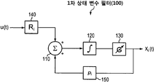
도 1은 1차 상태변수 필터의 블록도이다.
도 2는 2차 상태변수 필터의 제어표준형의 블록도이다.
도 3은 2차 상태변수 필터의 관측표준형의 블록도이다.
도 4는 본 별명의 원리에 따른 신호 필터링을 보여주는 흐름도이다.
도 5a는 도 1-3의 상태변수 필터내에서의 사용에 적합한 적분기의 회로도이다.
도 5b는 이상적 및 비 이상적 적분기의 주파수 응답을 보여주는 그래프이다.
도 5c는 비 이상적 적분기의 필터극점에 대한 효과를 보여주는 그래프이다.
도 6은 병렬의 상태변수 필터를 채용한 광대역 신호 처리기의 블록도이다.
도 7은 병렬의 1차 및 2차 상태변수 필터를 채용한 광대역 신호 처리기의 블록도이다.
도 8은 스트로보스코프(Stroboscopic) 신호처리 능력이 있는 광대역 신호 처리기의 블록도이다.
도 9a는 간섭탐지필터의 블록도이다.
도 9b는 도 9a에 표시된 간섭탐지필터를 사용한 스펙트럼분석을 보여주는 그래프이다.
도 10a는 간섭소거필터의 블록도이다.
도 10b는 도 10a에 표시된 간섭소거필터를 사용한 노치(notch) 필터링을 보여주는 그래프이다.
도 11은 본 별명의 원리에 따른 간섭탐지 및 소거를 보여주는 흐름도이다.
도 12는 대역소거필터와 스펙트럼 분석기를 채용한 송수신기의 블록도이다.
도 13은 가변필터(agile filter)의 뱅크를 채용한 소프트웨어 정의 라디오의 블록도이다.
도 14는 2차 상태변수 필터를 채용한 탭화된 탭화된 지연라인의 블록도이다.
도 15는 도 14에 표시된 탭화된 탭화된 지연라인에 기초한 상관기를 채용한 무선수신기의 블록도이다.
도 16은 본 발명의 원리에 따른 채널등화를 보여주는 흐름도이다.The foregoing will be apparent from embodiments of the invention to be described in more detail, which is illustrated in the accompanying drawings, wherein like reference numerals refer to like parts throughout the other aspects. It is emphasized that the drawings need not be to scale, but are shown to show embodiments of the invention.
1 is a block diagram of a first order state variable filter.
2 is a block diagram of a control standard type of the secondary state variable filter.
3 is a block diagram of an observation standard type of a secondary state variable filter.
4 is a flow chart showing signal filtering in accordance with the principles of the present nickname.
5A is a circuit diagram of an integrator suitable for use within the state variable filter of FIGS. 1-3.
5B is a graph showing the frequency response of ideal and non-ideal integrators.
5C is a graph showing the effect on the filter pole of a non-ideal integrator.
6 is a block diagram of a wideband signal processor employing parallel state variable filters.
7 is a block diagram of a wideband signal processor employing parallel primary and secondary state variable filters.
8 is a block diagram of a wideband signal processor with stroboscopic signal processing capability.
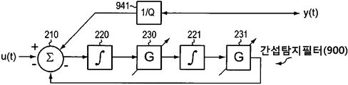
9A is a block diagram of an interference detection filter.
FIG. 9B is a graph showing spectral analysis using the interference detection filter shown in FIG. 9A.
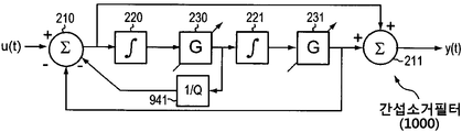
10A is a block diagram of an interference cancellation filter.
FIG. 10B is a graph showing notch filtering using the interference cancellation filter shown in FIG. 10A.
11 is a flowchart illustrating interference detection and cancellation in accordance with the principles of the present nickname.
12 is a block diagram of a transceiver employing a band cancellation filter and a spectrum analyzer.
13 is a block diagram of a software defined radio employing a bank of agile filters.
14 is a block diagram of a tapped tapped delay line employing a second order state variable filter.
FIG. 15 is a block diagram of a radio receiver employing a correlator based on the tapped tapped delay lines shown in FIG.
16 is a flow chart showing channel equalization in accordance with the principles of the present invention.
본 발명의 실시예들에 대한 상세한 설명이 이어질 것이다.Detailed description of the embodiments of the present invention will follow.
거대한 주파수 대역(예를 들면, 3.7 ~10.0 GHz) 전역에 신호 에너지를 정교하게 펼쳐놓는, 광대역과 초광대역(UWB)통신 시스템은, 많은 무선 어플리케이션에 대하여 전도가 유망하다. 광대역 통신의 많은 속성들-정확한 거리측정, 재료관통(penetration), 오버레이, 극한 환경에서 동작하는 저전력 시스템내의 다중경로페이딩에 대한 강건성-은 라디오주파수 식별자(RFID)와 같은 도전적인 군용 및 상업용 어플리케이션에 직면한 목표들과 직접적으로 관련된다. 또한, 기저대역에서 동작하는 광대역 시스템은 수신기에서 하향변환을 필요로 하지 않기 때문에, 수신기를 단순화시킨다.Broadband and ultra-wideband (UWB) communication systems, which precisely spread signal energy across large frequency bands (e.g., 3.7-10.0 GHz), are promising for many wireless applications. Many of the properties of broadband communications—accurate ranging, material penetration, overlays, and robustness to multipath fading in low-power systems operating in extreme environments—are used for challenging military and commercial applications such as radio frequency identifiers (RFIDs). It is directly related to the goals encountered. Also, a wideband system operating at baseband simplifies the receiver since it does not require downconversion at the receiver.
광대역시스템을 거대한 주파수 대역에 고르게 퍼져있는 에너지를 갖도록 설계하여 오버레이 요구사항을 만족시켜야 한다는 목표가 통신시스템 설계자들에게 명백해졌다. 특히, 사람들은 일반적으로 디지털 수신기, 일부 또는 풀 레이크 수신기를 위한 아날로그 상관기, 및 송신된 참조수신기(transmitted reference receivers)로부터의 극한의 대역폭(현재 7GHz, 잠재적으로 미래에는 더 큰)에 확장성이 있는 수신기 디자인을 선택한다. Broadband systems have energy spread evenly over large frequency bands The goal of designing to meet overlay requirements has become apparent to communications system designers. In particular, people are generally scalable to extreme bandwidth (currently 7 GHz, potentially larger in future) from digital receivers, analog correlators for some or full rake receivers, and transmitted reference receivers. Select the receiver design.
아날로그디지털(A/D) 변환기는 디지털 수신기의 대역폭과 동적 거리(해상도)를 제한한다. 현재, 기저대역 UWB 신호를 적절하게 샘플링할 수 있는 하이파이(high-fidelity) A/D 변환기는 특히 RFID 어플리케이션에 대해 지나치게 복잡하고 많은 전력을 소모한다. 다른 디지털 시스템은 낮은 해상도의 A/D 변환기에 의존하지만, 잘 동작하는 것은 아니다. 아날로그 상관기에 있어서, 대역폭이 커짐에 따라, 효율적인 에너지 포획을 위하여 레이크 핑거의 수가 증가하는데, 이에 따라, 회로 복잡도와 채널추정의 어려움이 증가한다. 비록 송신된 참조수신기는 중하정도의 데이터율의 동작에 매력적이지만, 이들은 UWB 어플리케이션을 위해 수신기에 거대한 대역폭 지연라인(delay line)을 요구한다.Analog-to-digital (A / D) converters limit the bandwidth and dynamic distance (resolution) of a digital receiver. Currently, high-fidelity A / D converters that can properly sample baseband UWB signals are overly complex and consume a lot of power, especially for RFID applications. Other digital systems rely on low resolution A / D converters, but they do not work well. In an analog correlator, as the bandwidth increases, the number of rake fingers increases for efficient energy capture, thereby increasing circuit complexity and channel estimation difficulty. Although the transmitted reference receivers are attractive for medium to moderate data rate operation, they require huge bandwidth delay lines at the receiver for UWB applications.
이제 디지털 신호 처리를 증대시키고 그러한 시스템의 대역폭 처리능력을 상당히 개선한 광대역 신호처리(WiSP)를 개시한다. 상기 WiSP시스템과 기술은 아날로그 도메인에 디지털 기능을 구현하고 확장시켜서 광대역신호에 대한 다목적 신호처리를 제공한다. 본 발명의 실시예는 상태변수기반의 아키텍쳐를 채용하여 명시가능한 정확도로 원하는 임펄스응답이나 전달함수(transfer function)를 구현한다. 중심주파수를 포함하는 모든 필터 파라미터는 낮은 데이터율로 실행되는 알고리즘, 광대역 디지털 신호프로세서(DSP) 또는 제어경로 내에서 실행되는 다른 적합한 제어요소들을 통해 제어되고 최적화될 수 있다. 광대역 신호처리기는 초미세 상보성 금속산화막 반도체 (CMOS:complementary metal-oxide-semiconductor)구조상에 구현되어, 10Ghz를 초과하는 대역폭을 갖는 신호를 포함하는, 광대역신호의 처리를 허용한다.We now introduce wideband signal processing (WiSP), which increases digital signal processing and significantly improves the bandwidth processing capabilities of such systems. The WiSP system and technology provide multi-purpose signal processing for wideband signals by implementing and extending digital functions in the analog domain. Embodiments of the present invention employ a state variable based architecture to implement the desired impulse response or transfer function with clarity. All filter parameters, including the center frequency, can be controlled and optimized through algorithms running at low data rates, broadband digital signal processors (DSPs), or other suitable control elements running within the control path. The broadband signal processor is implemented on a complementary metal-oxide-semiconductor (CMOS) structure to allow the processing of broadband signals, including signals having bandwidths in excess of 10 Ghz.
상기 WiSP 시스템과 장치의 실시예들은 동적으로 재구성가능한 필터를 포함하는데, 상기 필터는 광대역필터, 가변(agile) 필터, 적응형 필터, 이퀄라이저, 직접 중간주파수(IF) 송신기, 단일-측대역 변조기와 복조기로서 사용될 수 있다. 본 발명의 원리에 따라 만들어진 필터, 처리기, 이퀄라이저 및 탭화된 지연라인라인(tapped delay lines)은 액티브 RFID, 레이더, 이미징, 소프트웨어 정의 라디오, 인지라디오, 광대역처리기, 기기장치, 무선 고화질 멀티미디어 인터페이스를 포함하지만 이들에 한정되지 않는 다양한 종류의 어플리케이션에 사용될 수 있다. 상기의 컴포넌트와 어플리케이션들이 모든 것을 망라하는 것은 아니며, 본 발명의 원리에 따라 생산되고 사용되기에 적합한 대표적인 컴포넌트와 어플리케이션이다.
Embodiments of the WiSP system and apparatus include a dynamically reconfigurable filter, which includes a wideband filter, an agile filter, an adaptive filter, an equalizer, a direct intermediate frequency (IF) transmitter, a single-sideband modulator It can be used as a demodulator. Filters, processors, equalizers and tapped delay lines made in accordance with the principles of the present invention include active RFID, radar, imaging, software-defined radios, cognitive radios, broadband processors, instrumentation, and wireless high-definition multimedia interfaces. However, it can be used for various kinds of applications that are not limited to these. The above components and applications are not exhaustive and are representative components and applications suitable for production and use in accordance with the principles of the present invention.
아날로그 신호 처리를 위한 필터들(Filters for Analog Signal Processing FiltersFilters forfor AnalogAnalog SignalSignal Processing) Processing)
전형적인 신호처리시스템은 두 평면에서 작동한다. 상기 신호평면(S-평면)에서, 신호는 필터와 또 다른 처리연산을 사용하여 조작된다. 제어평면(C-평면)에서, 신호처리연산이 준비되고 조작된다. 예를 들면, 적응형 신호등화 시스템에서, 신호는 횡단선 필터를 통과하지만, 필터계수는 C-평면에 의해 제어된다. 오늘날 상기의 두 가지 기능은 모두 DSP에 의해 처리된다. 디지털 신호처리를 위한 근원적인 수학적 원리는 샘플링원리에 따르는 나이퀴스트 샘플링율 이상의 동기샘플링인 S-평면 이론에 근거한다. 말할 것도 없이, 이러한 기능성을 구현하는 시스템은 DSP, A/D 및 디지털아날로그(D/A)기술에 의존한다.Typical signal processing systems operate in two planes. In the signal plane (S-plane), the signal is manipulated using a filter and another processing operation. In the control plane (C-plane), signal processing operations are prepared and operated. For example, in an adaptive traffic light system, the signal passes through a cross line filter, but the filter coefficient is controlled by the C-plane. Today both of these functions are handled by the DSP. The fundamental mathematical principle for digital signal processing is based on the S-plane theory, which is a synchronous sampling above the Nyquist sampling rate according to the sampling principle. Needless to say, systems that implement this functionality rely on DSP, A / D, and digital analog (D / A) technologies.
여기에 제시된 실시예에서, S-평면은 10+GHz의 대역폭을 유지하면서 복잡한 아날로그 신호처리(신호경로는 항상 아날로그임)를 수행한다. 그러나, C-평면은 전통적인 A/D,D/A 및 DSP 아키텍쳐내에 구현된다. 실시예는 오늘날의 표준에 비하면 극도로 낮은 전력소모를 보여주는데, 이는 이들 하이브리드 시스템의 낮은 게이트 수와 블록 아키텍쳐 때문이다. In the embodiment presented here, the S-plane performs complex analog signal processing (signal path is always analog) while maintaining a bandwidth of 10+ GHz. However, the C-plane is implemented in traditional A / D, D / A and DSP architectures. The embodiment shows extremely low power consumption compared to today's standards because of the low gate count and block architecture of these hybrid systems.
필터들은 아날로그 신호 처리기들을 위한 빌딩-블록 컴포넌트들로서, 상기 신호 처리기들은 주파수와 관련하여 신호의 진폭 및/또는 위상 특성을 변경하여 S-평면내의 신호처리를 가능하게 한다. 필터들은 특정 주파수 범위 내의 신호들을 통과시키고, 다른 범위의 주파수는 저지하도록 사용된다. 대역통과필터는 주어진 대역 내에서 발생한 주파수들만 전송한다. 한편 노치(notch) 또는 대역소거필터는 지정된 주파수들은 제거하고 다른 주파수들은 방해받지 않고 통과하도록 한다. 저역통과필터와 고역통과필터는 각각 컷오프 주파수보다 더 높은 대역주파수와 더 낮은 대역주파수를 저지한다. 전역통과필터는 신호를 약하게 하지 않으면서 입력 신호상의 위상변위를 전달한다.Filters are building-block components for analog signal processors, which change the amplitude and / or phase characteristics of the signal with respect to frequency to enable signal processing in the S-plane. Filters are used to pass signals in a specific frequency range and to block frequencies in other ranges. The bandpass filter only transmits frequencies that occur within a given band. A notch or bandpass filter, on the other hand, eliminates specified frequencies and allows other frequencies to pass through undisturbed. The low pass filter and the high pass filter respectively block higher and lower band frequencies than the cutoff frequency. The global pass filter transmits the phase shift on the input signal without weakening the signal.
필터의 주파수응답은 출력과 입력신호의 라플라스변환(Laplace transform)비율인 전달함수에 의하여 수학적으로 표현될 수 있다. 이상필터(ideal filters)는 직사각 전달함수를 갖는데, 상기 전달함수는 통과대역과 저지대역간의 무한히 가파른 경계와 통과대역 내의 상수이득을 갖는다. 또한, 이상필터는 신호에 위상왜곡이 도입되는 것을 피하기 위하여 선형위상응답을 갖는다. 실제 필터들은 이상적인 응답을 근사(approximate)만 할 수 있다.The frequency response of the filter can be represented mathematically by a transfer function which is the Laplace transform ratio of the output and input signals. Ideal filters have a rectangular transfer function, which has an infinitely steep boundary between the passband and stopband and a constant gain within the passband. The anomaly filter also has a linear phase response to avoid introducing phase distortion into the signal. Real filters can only approximate the ideal response.
필터의 차수는 필터의 전달함수의 다항식 확장의 차수와 동일하다. 종래의 RF시스템에서, 높은 차수필터는 낮은 차수필터를 종속연결(따라서, 직렬연결)하여 구성된다. 예를 들면, 3차 필터는 1차 필터의 출력을 2차 필터의 입력에 연결함으로써 구성된다. 높은 차수필터들은 전형적으로 향상된 통과 대역성능을 갖고 낮은 차수필터보다 더 빠른 롤오프(저지대역내에서의 감쇠)를 갖는다.
The order of the filter is equal to the order of the polynomial extension of the filter's transfer function. In conventional RF systems, high order filters are constructed by cascading low order filters (and therefore in series). For example, the tertiary filter is constructed by connecting the output of the primary filter to the input of the secondary filter. High order filters typically have improved passband performance and have a faster rolloff (attenuation in the low band) than low order filters.
필터 설계, 구현 및 동작(Filter design, implementation, and behavior ( FilterFilter DesignDesign , , ImpementationImpementation , , andand Operation) Operation)
통상적으로, 필터를 설계할 때의 목표는 특정한 전달함수 또는 임펄스응답을 구현하는 것이다. 유리함수(rational function)에 부합하는 전달함수는 다음의 식을 갖는다Typically, the goal when designing a filter is to implement a specific transfer function or impulse response. The transfer function corresponding to the rational function has the following formula

상기 식에서 s = jω이고 단위는 rad*Hz 이다. 상기 분자에 대한 해는 필터들의 0 들이다; 상기 분모의 해는 필터들의 극점들이다. 상기 식에 대하여 부분 분수전개(partial fraction expansion)가 수행되고 역 라플러스변환이 수행됨으로써 어떤 임시함수라도 복소수 사인곡선(complex sinusoids)의 합으로서 표현될 수 있다. Where s = jω and the unit is rad * Hz. The solution to the molecule is the zeros of the filters; The solution of the denominator is the poles of the filters. By performing partial fraction expansion on the equation and performing inverse Laplus transform, any temporary function can be expressed as the sum of complex sinusoids.

상기 근사함수(approximation)는 상기 덧셈에 항들을 추가시킴으로써 임의의 정확도까지 정확하게 만들어질 수 있다.The approximation can be made precisely to any accuracy by adding terms to the addition.
방정식(2)에서처럼 복소수 사인곡선의 덧셈(summation)의 형태로 임펄스 응답에 대한 식을 전개하기 위하여, 파데 근사함수, Prony의 방법 또는 다른 적합한 방법이 R i 의 값과 y mn (t)의 P i 값을 결정하도록 채용될 수 있다. 일단 y mn (t)를 알면, 상태변수기법을 사용하는 것이 가능하다. 방정식(3)에 의해 묘사되는 시스템은 해 y(t)를 갖는데 이는 방정식(2)의 y mn (t)와 같은 형태이다. To develop the equation for the impulse response in the form of a summation of a complex sinusoid, as in equation (2), the Pade approximation function, Prony's method, or another suitable method is known as R i. And the value of y mn ( t ) P i May be employed to determine the value. Once y mn ( t ) is known, it is possible to use the state variable technique. The system described by equation (3) has a solution y ( t ), which is the same as y mn ( t ) of equation (2).

Prony의 방법이나 파데 근사함수를 적용하면 R i 와 P i 값의 목록이 산출되는데, 이중 몇 개는 실수이고, 몇 개는 복소수이다. 복소수 극점/나머지(complex pole/residue)쌍이 복소수 켤레(conjugate)쌍으로 발생하고, 다음과 같이 결합 될 수 있다. Applying Prony's method or Pade approximation, R i And P i A list of values is produced, some of which are real and some of which are complex. Complex pole / residue pairs occur as complex conjugate pairs and can be combined as follows.

상기 모든 필터 계수(a's와 b's)는 실수이다. 이러한 켤레쌍은 아래 자세하게 묘사된 이차 제어 및 관측표준형을 사용하여 실현될 수 있다. All of the filter coefficients a's and b's are real. Such a pair can be realized using the secondary control and observation standard described in detail below.
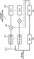
도 1은 방정식(2)와 (3)의 실수 해(real solutions)를 구현하기 위해 사용되는 1차 상태변수필터(100)를 보여준다. 상기 1차 상태변수필터(100)는 광대역 입력 u(t)에 대하여 작용을 하여 필터링된 출력 x 1 (t)을 생성한다. 나머지블록(140)은 입력의 나머지 R i 를 결정하고, 상기 R i 는 덧셈계수기(110)로 전달되어 필터링된 출력의 극점p i 와 결합 된다. 상기 덧셈계수기(110)는 나머지와 극점의 합계를 적분기(120)로 전달한다. 종래의 1차 상태변수필터와 달리, 본 발명의 1차 상태변수 필터(100)는 상기 적분기(120)의 출력에 대하여 동작하는 변수이득블록(130)을 포함한다. 상기 변수이득블록(130)은 상기 적분된 신호를 이득세팅 G에 따라서 증폭하거나 감쇠하여 필터링된 출력을 생성한다. 상기 변수이득블록(130)에 연결된 극점블록(150)은 필터링된 출력인 극점 P i 생성하고, 상기 필터링된 극점 P i 는 덧셈계수기(110)로 되돌려 보낸다. 상기 극점 블록(150)과 상기 나머지 블록(140)의 파라미터의 변경(즉 필터 탭 가중치를 변경시키면)은 필터중심 주파수와 통과 대역폭을 포함하는 상기 필터 전송특성을 변화시킨다. 1 shows a primary state
도 1에 도시된 상기 1차 상태변수 필터(100)를 재 조사하면 변수이득블록(130)의 효과가 매우 흥미롭다는 것을 알 수 있다. 상기 적분기(120)(라플라스 도메인내의 1/s에 동등한)에 의해서 선도되었을 때, 변수이득블록(130)은 신호를 증폭하기보다는 주파수 스케일로서 동작한다. 상기 변수이득블록(130)은 필터전달함수 T(s)를 T(s/G)로 변환하는데, 여기서 G는 상기 변수이득블록 (130)의 이득이다. s= jω= j2πf 일때, s를 1/G로 스케일링하면 T(s)의 주파수가 동일한 G의 인자에 의해 효과적으로 스케일링된다. G를 변화시키면 필터 통과대역의 중심주파수가 UWB대역에 전역으로 튜닝된다.Reexamination of the primary state
도 2와 도 3은 제어 및 관측 표준형 내의 2차 상태변수 필터들(200, 300)을 보여주는데, 이들은 각각 방정식(2)와 방정식(3)에 대한 2차(second-order) 해를 구현한다. 상기 두 공식은 수학적으로 동등하지만, 상기 관측형(300)은 추가적인 덧셈계수기(summer)를 필요로 하고, 다르게 구성된 입력과 출력을 갖는다. 도 1의 상기 1차 상태변수 필터(100)처럼, 상기 2차 필터들(200, 300)은 필터 통과대역의 중심주파수를 변화시키는 변수이득 블록들을 포함한다. 이들은 또한 방정식(4)의 전달함수의 계수(즉, a0,a1,a2,b0,b1,그리고 b2)를 나타내는 탭 가중치, 또는 분수이득블록을 포함한다. 상기 변수이득 블록처럼, 상기 분수이득 블록은 대응하는 계수에 따라서 신호를 증폭하거나 감쇠한다. 전형적으로 상기 변수 및 분수이득 블록은 신호를 -1 이상 1 이하의 정규화된 범위 내의 값으로 스케일 한다..2 and 3 show secondary state
도 2의 상기 제어 2차 상태변수 필터(200)는 광대역 입력 u(t)에 작용하여 필터링된 출력 x2(t)을 생성한다. 덧셈계수기(210)는 상기 광대역 입력을 분수이득블록들(240, 241)의 출력과 결합시킨다. 상기 덧셈계수기(210)는 상기 광대역 입력과 상기 분수이득블록 출력의 차이를 제3 분수이득 블록(242)으로 전달하고, 상기 제3 분수이득블록(242)은 상기 덧셈계수기 출력을 1/a2로 스케일링한다. 상기 분수이득 블록(242)은 상기 스케일된 덧셈계수기 출력을 적분기(220)와 분수이득블록(252)으로 전달하며, 상기 분수이득 블록(252)은 상기 스케일된 덧셈계수기 출력을 b2 로 스케일한다. The control secondary state
상기 적분기(220)가 상기 스케일된 신호를 적분한 후, 상기 적분된 결과신호를 변수이득블록(230)으로 전달하면, 상기 변수이득블록은 전달된 신호주파수를 이득 세팅 G1 에 따라 튜닝한다. 상기 변수이득블록(230)의 출력은 제 2 적분기(221) 및 분수이득블록들(241, 251)로 전달되고, 상기 분수이득 블록들(241,251)은 그 출력을 각각 a1과 b1으로 스케일 한다. 상기 제 2 적분기(221)는 상기 신호를 다시 적분하고, 그 결과인 제2 적분된 신호를 변수이득블록(231)으로 전달한다. 상기 변수이득블록(231)의 출력은 분수이득블록(240,250)으로 전달되어, 각각 a0와 b0로 스케일링 된다. 덧셈계수기(211)는 상기 분수이득블록들(250-252)의 출력을 결합하여 필터링된 출력을 제공한다.After the
도 3의 상기 관측 2차 상태변수 필터(300)는 광대역 입력u(t)에 작용하여 필터링된 출력 x2(t)을 생성하는데, 이는 도 2의 필터(200)와 상당히 같은 방법으로 수행된다. 그러나, 다만, 분수이득 블록(350,351,352)은 상기 광대역 입력을 각각 수량 b0,b1,및 b2로 스케일하여 그 결과인 상기 스케일된 출력을 각각 덧셈계수기(310, 311 및 312)로 전달한다. 상기 덧셈계수기(310)는 분수이득블록(340)의 스케일된 출력을 상기 분수이득블록(350)의 출력과 결합하거나 또는 상기 분수이득블록(350)의 출력으로부터 감산하여 결합된 신호를 제공한다. The observed secondary state variable filter 300 of FIG. 3 acts on the wideband input u (t) to produce a filtered output x 2 (t), which is performed in much the same way as the
적분기(320)는 상기 결과신호를 적분하여, 적분된 신호를 변수이득블록(330)으로 전달하며, 상기 변수이득블록(330)은 통과된 신호주파수를 이득세팅에 따라 튜닝한다. 제2 덧셈계수기(311)는 변수이득블록(330)의 출력을 분수이득블록(341,351)의 출력과 결합하여 제2 결합된 출력을 제공한다.The
제2 적분기(321)은 상기 제2 결합된 출력을 적분하여, 결과인 제2 적분된 신호를 제2 변수이득블록(331)로 전달한다. 제3 덧셈계수기(312)는 상기 제2 변수이득블록의 출력을 분수이득블록(352)의 출력과 결합하여 제3 결합된 신호를 제공한다. 분수이득블록(342)는 상기 제3 결합된 신호를 1/a2로 스케일링하여 필터링된 출력을 제공한다. 상기 필터링된 출력은 분수이득 블록(340,341)으로 전달되어, 상기 필터링된 출력은 각각 a0 와 a1 으로 스케일링된다. The
도1 내지 3의 1차 및 2차 상태 변수필터는 추가적인 적분기와 변수이득블록을 적절하게 편입하거나 제거함으로써 어떤 차수로도 일반화할 수 있다. n차상태 변수필터는 변수이득 블록을 n개 적분기들 각각의 출력과 연결되도록 구성될 수 있다. 더 높은 차수 상태변수 필터는 필터 전역의 다양한 포인트에서 신호를 스케일링하고 결합할 수 있도록 구성된 추가적인 함수이득 블록과 덧셈계수기를 포함할 수도 있다. 함수 이득블록의 스케일링 계수를 0 또는 1로 설정하면(상기 필터 구성에 따라), 상기 함수이득블록의 필터의 동작에 미치는 효과를 효과적으로 진압할 수 있다.The primary and secondary state variable filters of FIGS. 1-3 can be generalized to any order by incorporating or removing additional integrators and variable gain blocks as appropriate. The nth order state variable filter may be configured to couple the variable gain block with the output of each of the n integrators. Higher order state variable filters may include additional function gain blocks and add counters configured to scale and combine signals at various points throughout the filter. If the scaling factor of the function gain block is set to 0 or 1 (depending on the filter configuration), the effect on the operation of the filter of the function gain block can be effectively suppressed.
도 4는 본 발명의 원리에 따른 기본신호 필터링(400)을 보여준다. 우선, 광대역 입력(402)은 극점(418)과 결합(404)하여, 결합된 신호(406)를 생성하는데, 이때, 극점(418)은 신호필터링(400)을 통과해 나온 필터링된 신호(416)로부터 결정된다. 더 높은차수 필터링에서, 상기 극점(418)은 필터링된 신호(416)가 분수이득계수로 스케일링 됨으로써 파생될 수 있다. 상기 결합된 신호(406)는 적분되어(408) 적분신호(410)을 생성하고, 상기 적분신호(410)는 변수이득(414)에 의해 증폭되어(412) 상기 필터링된 신호(416)를 생성한다. 상기 변수이득(414)을 변화시키면 필터링된 신호(416)의 중심주파수가 전위된다.4 shows basic signal filtering 400 in accordance with the principles of the present invention. First, wideband input 402 combines 404 with pole 418 to produce a combined signal 406, where pole 418 is filtered signal 416 that has passed through signal filtering 400. Is determined from In higher order filtering, the pole 418 can be derived by scaling the filtered signal 416 by a fractional gain factor. The combined signal 406 is integrated 408 to produce an integrated signal 410, and the integrated signal 410 is amplified by variable gain 414 412 to generate the filtered signal 416. do. Changing the variable gain 414 shifts the center frequency of the filtered signal 416.
상태 변수필터를 위한 적분기(Integrator for State Variable Filter ( IntegratorsIntegrators forfor StateState VariableVariable FiltersFilters ))
도 5a는 도 1-3의 상태변수 필터내의 사용에 적합한 트랜스컨덕터 기반의 적분기(500)를 보여준다.(물론, 도 1-3의 상태변수 필터들은 도 5a의 적분기(500)외에 다른 적합한 적분기를 사용할 수 있다.) 상기 적분기는 제2와 제3 전력공급터미널(520,522) 사이에 직렬로 연결된 4개의 금속산화막 반도체 전계 효과 트랜지스터(모스펫:MOSFETs)(510-513)를 포함한다. 특정 실시예에서 상기 모스펫(510-513)은 65nm 상보성금속산화막반도체(CMOS) 처리기를 이용하여 처리된다. 상기 P-채널인 증가형모드(Enhancement-mode) 모스펫(510)의 소스와 드레인은 제1 전력공급단자와 상기 P-채널인 증가형모드 모스펫(511)의 소스에 각각 연결된다. 도 5a에서 보여지듯이, 상기 모스펫들(510,511)의 게이트는 각각 1.35V와 0.9V에서 바이어스되어 있다.5A shows a transconductor based integrator 500 suitable for use in the state variable filters of FIGS. 1-3. (Of course, the state variable filters of FIGS. 1-3 may include other suitable integrators other than the integrator 500 of FIG. 5A. The integrator includes four metal oxide semiconductor field effect transistors (MOSFETs) 510-513 connected in series between the second and third
상기 모스펫(511)의 드레인은 출력노드(541)에 연결되는데, 상기 출력노드는 그라운드에 연결된 축전기(531)를 사용하여 필터링될 수도 있다. 상기 모스펫(511)의 드레인은 또한 N-채널인 증가형모드 모스펫(512)의 소스에 연결되고, 상기 증가형모드 모스펫(512)은 상기 N-채널인 증가형모드 모스펫(513)의 소스에 전기적으로 연결된다. 상기 모스펫(512)의 게이트는 0.9V에서 바이어스되는 반면, 상기 모스펫(513)의 게이트는 축전지(530)로 구성된 고역 통과필터를 경유하여 입력노드(540)에 연결되며 또한 0.45V 전위에 연결된 레지스터(550)에 연결된다. 상기 모스펫(513)의 드레인은 그라운드에 연결된다.The drain of the
도 5b는 실제(즉, 비 이상적) 적분기에 대한 주파수응답 그래프를 보여준다. 이상적인 적분기는 도 5B에 도시된 20 dB/decade 응답처럼 모퉁이(corner)가 없는 선형주파수 응답을 갖는다. 그러나 실제 적분기는 완벽한 선형이 아닌 주파수응답을 갖는다. 도 5B에 도시된 것처럼, 주파수 응답은 상기 제1극점ωa미만의 주파수에서 일정하다. 제2극점ωb위쪽의 주파수에서 응답은 -20 dB/decade에서 -40 dB/decade로 떨어진다. 이러한 유한대역폭과 유한이득효과는 필터성능을 저하시킨다. 5B shows a frequency response graph for a real (ie, non-ideal) integrator. An ideal integrator has a cornerless linear frequency response, such as the 20 dB / decade response shown in FIG. 5B. However, the real integrator has a frequency response that is not perfectly linear. As shown in Fig. 5B, the frequency response is constant at frequencies below the first pole ω a . At frequencies above the second pole ω b the response drops from -20 dB / decade to -40 dB / decade. This finite bandwidth and finite gain effect degrades the filter performance.
도 5c는 실제(즉, 비이상적) 적분기의 유한이득과 유한대역폭이 9차 필터의 성능에 미치는 효과를 보여준다. 비 이상적인 조건에서, 상기 필터의 극점은 선 Re(s)=-(ωa+ωb)/2 (ωa 와 ωb 는 필터 전달함수의 해이다)에 대해 실축을 따라 대칭적으로 분포한다. 유한대역폭효과는 의도된 응답을 오염시키는 스퓨리어스 시간신호를 생성하는 스퓨리어스(spurious) 극점(502)의 출현을 유발한다. 하지만 만일 스퓨리어스 극점이 의도된 극점에서 멀리 떨어져 있다면, 스퓨리어스 시간신호는 무시해도 될 만큼 충분히 작다.5C shows the effect of the finite gain and finite bandwidth of a real (ie, non-ideal) integrator on the performance of a ninth order filter. Under non-ideal conditions, the poles of the filter are symmetrically distributed along the real axis with respect to the line Re (s) = − (ω a + ω b ) / 2 (ω a and ω b are solutions of the filter transfer function). The finite bandwidth effect causes the appearance of a spurious pole 502 that produces a spurious time signal that contaminates the intended response. However, if the spurious pole is far from the intended pole, the spurious time signal is small enough to be ignored.
유한이득효과는 의도된 극점들(504)을 다른 위치(506)로 주파수 이동하도록 만든다. 이들 유한이득효과는 필터 분자이득계수를 조정하여 의도된 극점의 위치(504)를 그대로 Re(s)축을 따라 이동시켜서, 상기 실제극점(504)이 최초에 의도된 극점의 위치(506)에 맞추어지도록 함으로써 완화될 수 있다. 즉, 만일 실제극점(504)이 s=-1.5에 있고 의도된 극점(506)이 s=-1에 있다면, 의도된 극점을 s=-0.5로 이동시키면 실제극점의 위치는 -1로 이동되어 비 이상성이 보상된다.
The finite gain effect causes the intended poles 504 to frequency shift to another location 506. These finite gain effects adjust the filter molecular gain coefficients to shift the intended pole position 504 as it is along the Re (s) axis, so that the actual pole 504 matches the originally intended pole position 506. Can be mitigated. That is, if the actual pole 504 is at s = -1.5 and the intended pole 506 is at s = -1, moving the intended pole to s = -0.5 causes the position of the actual pole to move to -1. Non-ideality is compensated for.
상태변수필터를 갖는 광대역 프로세싱(Broadband processing with state variable filter WidebandWideband ProcessingProcessing withwith StateState VariableVariable FiltersFilters ))
상기 상태변수필터는 종속접속되고 이들의 출력들이 합산되어 방정식(2)의 전달함수 Tmn(s), 또는, 대응하는, ymn(t)를 실현할 수 있다. 예제 아키텍쳐에서, 필터는 덧셈계수기, 적분기, 변수이득블록 및 함수이득블록을 포함하는 유닛블록으로 분할될 수 있다. 반복적인 아키텍쳐는 몇 개의 유닛블록을 가진 CMOS 칩을 효율적으로 생성할 수 있게 하는데, 상기유닛블록의 계수는 유리함수를 실현하거나 임펄스 응답을 모방하도록 프로그램될 수 있다.The state variable filters can be cascaded and their outputs summed to realize the transfer function T mn (s), or, correspondingly, y mn (t) of equation (2). In the example architecture, the filter may be partitioned into unit blocks that include an adder, an integrator, a variable gain block, and a function gain block. Iterative architecture enables efficient generation of CMOS chips with several unit blocks, the coefficients of which can be programmed to realize a rational function or to mimic the impulse response.
예를 들면, 도 6은 광대역 입력 u(t)에서 병렬로 동작하는 m차 상태변수 필터(610)와 n차 상태변수 필터(620)를 포함하는 광대역신호 처리기(600)를 보여준다. 덧셈계수기(630)는 필터들(610, 620)의 각 출력xm(t)와 xn(t)를 결합하여, 처리된 출력 ymn(t)을 생성한다. 상기 집합필터(aggregate filter) n+m차는 상기 개별필터(610, 620)의 차수의 합이며, 이때 n과 m은 양의 정수이다. 상기 개별필터 610과 620은 실시예에 따라 같은 차수일 수도 있고 다른 차수일 수도 있다. 또한, 상기 처리기(600)의 전달함수는 탭 가중치 또는 상기 개별필터(610, 620)의 분수이득을 조정함으로써 조정될 수 있다. For example, FIG. 6 shows a wideband signal processor 600 including an mth order state
다른 광대역신호 처리기는 같은 입력에 대해서 병렬적으로 동작하는 더 많은 필터를 포함할 수 있을 것이다. 이러한 추가적인 필터들은 또한 처리된 출력을 제공하기 위하여 일반적인 덧셈계수기(예를 들면, 덧셈계수기 630)에 연결된다. 둘 이상의 상태변수필터를 갖는 실시예에서, 상기 집합필터 차수는 상기 개별필터 차수들의 합이다.Other wideband signal processors may include more filters that operate in parallel on the same input. These additional filters are also connected to a general add counter (eg, add counter 630) to provide a processed output. In an embodiment having two or more state variable filters, the aggregate filter order is the sum of the individual filter orders.
도 7은 다른 광대역 신호 처리기(700)를 보여주는데, 상기 처리기(700)는 1차 상태변수 필터들(710-1 부터 710-k)과 2차 상태변수 필터들(720-1 ~ 720-l)을 포함하는데, 이들은 도 1 ~ 3에 적절하게 도시되어 있다. 상기 필터들(710,720)은 광대역 입력 u(t)에 대해 병렬로 동작하여, 각각 출력 ![]()
![]()
![]()
![]()
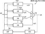
예를 들면, 스펙트럼 분석을 수행하도록 구성된 프로세스(700)는 상기 DSP(734)를 사용하여 상기 변수이득블록의 스케일된 이득계수를 -1 에서 1로 상승시킴으로써, 필터의 중심주파수를 스위핑할 수 있다. 상기 변수 및 분수블록의 이득 계수를 재프로그래밍하면 상기 필터극점과 나머지가 변경되어, 각 필터들(710a-k, 720a-l)의 통과대역폭, 형태 및 중심주파수가 변경된다. 상기 DSP (734)는 이러한 조정이 동적이고 적용성 있게 수행될 수 있도록 하여, 가변 필터링, 적응형 필터링 그리고 또 다른 유사한 신호 프로세싱 태스크의 수행을 가능하게 한다. 또한, 개별필터는 상기 변수 및 분수이득블록의 계수를 변화시킴으로써 효과적으로 전환(turn off)될 수 있다. For example, a process 700 configured to perform spectral analysis may sweep the center frequency of the filter by raising the scaled gain coefficient of the variable gain block from -1 to 1 using the
도 8은 또 다른 광대역 신호 프로세스(800)를 보여주는데, 이 프로세스는 스트로보스코프(Stroboscopic) 측정과 제어가 가능하다. 상기 프로세스(800)는 10x 필터블록(801)과 1x 필터블록(802)를 포함하는데, 상기 필터블록(801, 802)은 광대역 신호 u(t)에서 병렬로 동작한다. 각 블록(801, 802)은 처리된 출력을 제공하는 덧셈계수기에 병렬로 연결된 1차와 2차 필터를 포함한다. 10x 필터블록(801) 내에, 1차와 2차 필터(810, 820)는 -1 ~ 1 범위의 이득계수를 갖는 변수 및 분수이득블록을 가지며, 처리된 출력 y(t)(871)을 제공하도록 동작한다. 8 shows another wideband signal process 800, which is capable of stroboscopic measurement and control. The process 800 includes a 10x filter block 801 and a 1x filter block 802, wherein the filter blocks 801, 802 operate in parallel on the wideband signal u (t). Each block 801, 802 includes a first and second filter connected in parallel to an add counter that provides a processed output. Within the 10x filter block 801, the primary and
그러나 1x 필터 블록(802)에서, 1차와 2차 필터(811, 821)의 이득계수는 오직 -0.1 ~ 0.1의 범위 내에 있다. 결과적으로, 1x 필터 블록(802)의 출력은 처리된 출력 y(t)(871)의 저역통과 버젼(872)이다 (이경우, 상기 처리된 출력 주파수의 10분의 1정도에서의 저역통과된). ADC(832)는 DSP(834)에 연결된 저역통과신호(872)를 디지털화한다. 도 8에 나타난 것처럼, 저역통과 필터링과 디지털변환은 전대역(fullband)출력(871)을 이득 범위율(ratio of gain spans)과 동일한 스트로보 주파수에서 스트로보스코피하게 샘플링하는 것과 동등하다. 필터링은 ADC(832)에 대한 샘플율 요건을 완화시켜서, 상대적으로 큰 비트강도(bit depth)(즉 큰 동적범위)를 갖는 상대적으로 느린 ADC(832)를 사용할 수 있게 한다. 상기 DSP(834)는 또한 더 낮은 샘플율에서 동작하여, 규모, 복잡도 및 전력소모를 줄여준다.However, in the 1x filter block 802, the gain coefficients of the primary and
상기에 기술된 것처럼, 상기 DSP(834)는 동적 또는 적용성 있게 상기 1x 필터블록(802)의 필터(811,812) 내의 상기 이득블록 계수를 변경시킬 것이다. 두 필터블록(801, 802)은 연결되어있기 때문에, 10x 필터블록(801)의 이득계수는 1x 필터블록(802) 계수의 변경을 추적하여 10:1의 비율로 변경될 것이다. 따라서, 상기 DSP(834)가 상기 저역통과된 신호(871)를 변경 조정함에 따라, 상기 처리된 출력 (870)도 동일하게 변경되어 주파수 증강(Frequency-magnified) 버젼이 생성된다.
As described above, the
재구성가능한 상태변수필터를 사용한 간섭탐지와 소거(Interference Detection and Elimination Using Reconfigurable State Variable Filters InterferenceInterference DetectionDetection and and RejectionRejection UsingUsing ReconfigurableReconfigurable StateState VariableVariable FiltersFilters ))
초창기, UWB시스템과 관련된 우려는 타 시스템상에 그들 신호가 미칠 영향이었다. 그 이후로는, UWB 시스템 구현에 있어서 명백해진 주요한 문제점은, 거대한 대역폭 수신기 프런트엔드가 많은 간섭자를 통과시키며 수신기의 작동을 어렵게 하는 것이었다. 샘플 간섭자는 레이더, 데이터링크, 공항 착륙시스템 및 IEEE 802.16e 모바일시스템과 같은 그 밖의 RF시스템을 포함한다. 간섭자는 특히 군용 어플리케이션에서 문제가 되는데, 여기서 고출력 레이더가 대역내로 떨어질 수 있다. In the early days, concerns about UWB systems were the impact of their signals on other systems. Since then, the major problem that has become apparent in the implementation of UWB systems has been that large bandwidth receiver frontends pass many interferers and make the operation of the receiver difficult. Sample interferers include radar, datalinks, airport landing systems, and other RF systems such as the IEEE 802.16e mobile system. Interferers are a problem, especially in military applications, where high power radars can fall into band.
비록 극도의 광대역 시스템이 간섭자를 소거할 수 있도록 하는 신호처리기술이 있지만, 그러한 간섭자는 수신기 RF 회로소자를 비선형으로 조종하고 신호처리가 발생하기 전에 정보수령을 파괴한다. 이에 따라 전체적인 수신기 사슬을 고려하는 종합적인 접근방법이 필요하다. 개시된 발명의 실시예는 스펙트럼분석기와 소거필터로서 동작하도록 구성된 동적으로 재구성가능한 상태변수필터를 사용하여 간섭자를 탐지하고 소거할 수 있다. 이는 아래에 좀 더 구체적으로 설명된다. Although signal processing techniques allow extreme broadband systems to cancel interferers, such interferers manipulate the receiver RF circuitry nonlinearly and destroy the reception of information before signal processing occurs. This requires a comprehensive approach that takes into account the entire receiver chain. Embodiments of the disclosed invention can detect and cancel interferers using a dynamically reconfigurable state variable filter configured to operate as a spectrum analyzer and cancellation filter. This is explained in more detail below.
예시된 간섭탐지 기법(Schemes)은 주파수-가변(frequency-agaile)과 상기에 기술된 상태변수기법을 사용하는 하이큐(high-Q) 대역통과 필터를 만들어 내는 것을 포함한다. 필터 중심주파수는 대역을 가로지르는 간섭파워를 특징을 규정하기 위하여 UWB 대역을 가로질러 스캐닝 될 수 있다. Exemplary interference detection schemes include creating a high-Q bandpass filter using frequency-agaile and the state variable technique described above. The filter center frequency can be scanned across the UWB band to characterize the interference power across the band.
일반적으로, 2차 필터의 전달함수는 다음과 같이 주어진다.In general, the transfer function of the secondary filter is given by

상기 ωr은 의도된 중심 주파수이고, Q는 품질인자이다. 각주파수(angular frequency)를 1/2π Hz, 즉, ωr = 1rad/s, 로 정규화하면, 전달함수의 형태가 다음과 같이 변경된다. Ω r is the intended center frequency and Q is the quality factor. When the angular frequency is normalized to 1 / 2π Hz, that is, ω r = 1rad / s, the shape of the transfer function is changed as follows.

상기 함수는 도 2와 도 3에 각각 나타나듯이 제어 및 관측표준 상태변수 아키텍쳐를 사용하여 구현될 수 있다. 상기 대역통과필터의 중심주파수는 이득블록 G의 값을 조정함으로써 UWB대역을 가로질러 스위핑될 수 있다. 이러한 스위핑이 진행됨에 따라 UWB 채널을 가로지르는 간섭파워의 특징이 규정될 수 있다.The function can be implemented using a control and observation standard state variable architecture as shown in FIGS. 2 and 3, respectively. The center frequency of the bandpass filter can be swept across the UWB band by adjusting the value of the gain block G. As this sweeping proceeds, the characteristics of the interference power across the UWB channel can be defined.
도 9a는 도 2의 제어 2차 상태변수 필터(200)의 분수이득블록(240-242)과 또 다른 분수이득 블록(250-252)의 값을 조정하여 형성되는 간섭탐지필터(900)를 보여준다. 구체적으로, 블록들(250,252)의 분수이득은 0으로 설정되고(b0=b2=0); 블록(240, 242 및 251)의 분수이득은 1로 설정되고(a0=a2=b1=1); 블록(941)의 분수이득은 품질인자의 역수로 설정된다(a1= 1/Q). 품질인자 Q 는 필터 통과대역의 파형과 폭을 제어한다. 위에서 언급되었듯이, 필터이득 G는 중심주파수를 제어한다.FIG. 9A illustrates an interference detection filter 900 formed by adjusting the values of the fractional gain blocks 240-242 and another fractional gain blocks 250-252 of the control secondary state
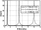
도 9b는 도 9a의 간섭탐지필터(900)에 의해 수행되는 UWB 주파수 스위핑을 보여주는 그래프이다. 상기 스위핑은 k의 이득을 적분단계에 도입하고, 2차 이득 G를 0.1로 설정하면서 1GHz에서 시작한다. 시스템은 G를 0.1에서 최종값 1.0까지 점진적으로 증가시키면서 UWB 대역 전역에 걸쳐 스위핑한다. 주파수 스위프 필터에 의하여 전송된 신호의 측정은 대역내(in-band) 간섭자들과 잡음소스들의 스펙트럼 맵을 만들어낸다.FIG. 9B is a graph showing UWB frequency sweeping performed by the interference detection filter 900 of FIG. 9A. The sweeping starts at 1 GHz, introducing a gain of k into the integration stage and setting the secondary gain G to 0.1. The system sweeps across the UWB band, gradually increasing G from 0.1 to a final value of 1.0. The measurement of the signal transmitted by the frequency sweep filter produces a spectral map of in-band interferers and noise sources.
일단 UWB 대역의 잡음 프로파일 특징이 규정되면, 상기에 묘사된 상태변수테크닉은 제어가능한 대역폭과 중심주파수를 갖는 대역저지 노치(Notch)필터를 구성하도록 적용될 수 있다. 이러한 소거필터들을 간섭자와 잡음소스 주파수에 놓는 것은 간섭파워를 제거하고 신호대잡음비율(SNR)을 최대화한다. 예를 들어, 다음 식의 전달함수를 갖는 2차 대역저지 노치필터를 고려해 보자. 
상기 ωr은 의도된 중심 주파수이고, Q는 품질인자이다.Ω r is the intended center frequency and Q is the quality factor.
전달함수/상태변수필터의 계수와 이득을 조정함으로써, Q와 노치(Notch)의 중심주파수는 수정될 수 있다. By adjusting the coefficients and gain of the transfer function / state variable filter, the center frequency of Q and notch can be modified.
도 10a는 도 2의 제어 2차 상태변수 필터(200)의 분수이득블록(240-242)과 또 다른 분수이득블록(250-252)의 값을 조정하여 형성되는 간섭소거(대역저지)필터(1000)을 보여준다. 구체적으로, 상기 블록(250, 251)의 분수이득은 0으로 설정되고(b0=b1=0); 블록(240, 242 및 252)의 분수이득은 1로 설정되고(a0=a2=b2=1); 블록(941)의 분수이득은 품질인자의 역수로 설정된다(a1= 1/Q). 품질인자 Q 는 필터소거 대역의 파형과 폭을 제어하며, 필터이득 G는 중심주파수를 제어한다.FIG. 10A illustrates an interference cancellation (Band Stop) filter formed by adjusting the values of the fractional gain blocks 240-242 and another fractional gain blocks 250-252 of the control secondary state
도 10b는 중심이 3.6 GHz, 5.8 GHz, 9.2 GHz 에 있고, 각각 0.36, 0.58, 0.92의 상대이득을 갖는 대역저지필터(1000)의 주파수응답을 보여준다. 상기 필터의 통과대역은 Q의 값을 변화시킴으로써 변경될 수 있다. 만일 간섭이 다소 더 크게 펼쳐져 있지만, 여전히 상대적으로 협 대역폭이라면, 다중오프셋 대역저지 노치필터(Multiple offset band stop notch filters)가 간섭을 저지하기 위하여 종속연결될 수 있다. 10B shows the frequency response of the
도 11은 본 발명의 원리에 따른 간섭탐지와 소거를 보여주는 흐름도이다. 먼저, 필터링된 신호(1106)를 만들어내기 위하여 광대역 입력(1102)에 대해 동작하는 상태변수 필터의 변수이득을 증강시킴으로써(ramp) 관심대역(예를 들면, UWB 대역)이 탐색된다(1104). 상기 필터중심주파수가 대역 전역을 탐색하기 때문에, 필터링된 신호(1106)는 상기 대역의 특징을 규정(1108)하는데 사용될 수 있다. 특성의 규정(1108), 또는 측정은 대역 내(in-band) 간섭자의 주파수위치 (111O)를 밝혀낸다. 다음으로, 대역저지, 또는 소거 필터들은 동적으로 조정가능한 변수와 분수이득계수(1114)를 사용하여 상태변수필터를 재구성(1112)함으로써 간섭자 주파수(1110)에 배치될 수 있다. 상기 재구성가능한 대역저지필터는 탐지된 간섭자를 소거(1116)하여 소거된 신호(1118)를 생성한다.
11 is a flowchart illustrating interference detection and cancellation in accordance with the principles of the present invention. First, a band of interest (e.g., UWB band) is searched (1104) by ramping the variable gain of a state variable filter operating on wideband input 1102 to produce filtered signal 1106. Since the filter center frequency searches across the band, the filtered signal 1106 can be used to define the characteristics of the band 1108. The specification 1108, or measurement of the characteristic, reveals the frequency location 1110 of the in-band interferer. Next, bandstop, or cancellation filters may be placed at the interferer frequency 1110 by reconstructing 1112 the state variable filter using the dynamically adjustable variable and fractional gain coefficient 1114. The reconfigurable bandstop filter cancels 1116 the detected interferer to produce an canceled signal 1118.
FSRFSR -- UWBUWB 송수신기 Transceiver 를To 사용한 RFID( RFID used RFIDRFID UsingUsing FSRFSR -- UWBUWB Transceivers) Transceivers)
RFID 태그는 일반적으로 매우 작고, 극도의 저전력 패키지내에서 강건한 통신과 정확한 위치 모두를 제공해야 한다. 많은 다양한 환경에서, RFID 통신은 또한 적군의 통신방해와 친숙한 레이더로부터의 간섭에 면역성이 있어야한다. 초광대역(UWB) 라디오는 그러한 어플리케이션을 위한 유망한 해법을 제시하지만, UWB 시스템은 항상 거대한 대역폭의 신호를 위한 수신기의 구현이 어려울 것이라는 우려가 걸림돌이었다. 게다가, UWB 시스템의 고유의 넓은 수신기 대역폭 때문에 상기 UWB시스템은 특히 대역내(in-band) 간섭과 전파방해에 민감하다. RFID tags are generally very small and must provide both robust communications and accurate location in extremely low power packages. In many different environments, RFID communication must also be immune to interference from enemy forces and familiar radars. While ultra-wideband (UWB) radios offer a promising solution for such applications, there has been a concern that UWB systems will always find it difficult to implement receivers for large bandwidth signals. In addition, because of the inherent wide receiver bandwidth of the UWB system, the UWB system is particularly sensitive to in-band interference and jamming.
주파수 편이참조 초광대역(FSR-UWB:Frequency shifted reference-Ultra Wideband)아키텍쳐는 RFID를 포함하여 극도의 저전력의 적당한 데이터율 어플리케이션들내의 많은 구현이슈들에 역점을 둔다. 본 발명의 실시예는 극도의 광대역 시스템내의 간섭완화를 위한 새로운 접근방법을 우리의 FSR-UWB 솔루션의 저전력 송수신기 구현과 조화시킴으로써 상기의 우려들에 역점을 둔다. 결과는 RFID 어플리케이션을 위한 저전력의 간섭소거시스템이다.The frequency shifted reference-Ultra Wideband (FSR-UWB) architecture emphasizes many implementation issues in extremely low power, moderate data rate applications, including RFID. Embodiments of the present invention address these concerns by harmonizing a novel approach to interference mitigation in extreme broadband systems with the low power transceiver implementation of our FSR-UWB solution. The result is a low power interference cancellation system for RFID applications.
상기 RFID기술의 실시예는 저전력 아키텍쳐, 적응형 간섭억제 회로, 및 수정된 펄스 성형능력(modified pulse shaping capability)을 지닌 실시간 위치탐지(real-time location)를 위한 FSR-UWB시스템이다. 예를 들면, 상기 FSR-UWB 기술은 의사가 병원 안의 구명장비를 신속하게 찾을 수 있도록 한다. 디트로이트에 있는 공장은 FSR-UWB 기술을 사용하여 싱가포르의 공급자가 보낸 상품을 추적할 수 있을 것이다. 해운회사 또는 물류회사 직원은 상자를 열지 않고도 화물의 내용물과 만료일을 확인할 수 있다. 화학공장의 안전담당자는 위험한 지역에 있는 작업자들의 움직임을 추적하여, 사고발생시 그들의 위치를 정확하게 탐지할 수 있다. 상기 어플리케이션은 거의 무한하다.An embodiment of the RFID technology is a FSR-UWB system for real-time location with low power architecture, adaptive interference suppression circuitry, and modified pulse shaping capability. For example, the FSR-UWB technology allows doctors to quickly find life preservers in hospitals. The Detroit-based plant will use FSR-UWB technology to track goods sent from suppliers in Singapore. Shipping company or logistics company personnel can check the contents and expiration date of the cargo without opening the box. The safety officers of chemical plants can track the movements of workers in hazardous areas and accurately detect their location in the event of an accident. The application is almost endless.
경쟁 RFID 기술들은 상기의 FSR-UWB기술과 같은 위치탐지의 정확성을 성취할 수도 없고, 동일한 환경범위에서 잘 수행될 수도 없다. 433 MHz와 2.4 GHz 에서 동작하는 RFID 태그는 금속이나 물을 함유한 표면에 실렸을 때 잘 작동하지 않는다. 이들은 또한 환경에 따라서 3m 내지 10m의 최소 식별거리(resolution)를 갖는데, 이는 많은 새로운 어플리케이션에 부적합하다. 반대로, 상기 FSR-UWB 시스템은 금속이나 물에 의한 영향을 받지 않으며, 다중경로환경에서 잘 수행된다. 상기 FSR-UWB 시스템은 전력소모가 작고, 30cm 보다도 좋은 최소식별거리를 갖는 자산의 위치를 탐지할 수 있다.Competitive RFID technologies may not achieve the same positioning accuracy as the FSR-UWB technology above, nor may they perform well in the same environment. RFID tags operating at 433 MHz and 2.4 GHz do not work well when mounted on metal or water-containing surfaces. They also have a minimum resolution of 3m to 10m, depending on the environment, which is unsuitable for many new applications. In contrast, the FSR-UWB system is not affected by metal or water and performs well in a multipath environment. The FSR-UWB system can detect the location of an asset with low power consumption and a minimum identification distance of more than 30 cm.
도 12는 RFID 태그나 판독기(reader)로서의 사용에 적합한 송수신기(1200)의 블록다이어그램을 보여준다. 안테나(1202)는 저전력컨트롤러(1220)에 의해 제어되면서 UWB 신호를 전송하고 수신한다. 상기 안테나(1202)는 6 dBi의 이득을 갖는 테이퍼형 슬롯 안테나일 수 있다. 이는 편광각 설정을 위해 접혀지고, 기계적 지지를 위해 거푸집 블록안에 놓이는 얇은 굴절성의 절연체에 인쇄될 수 있다. 12 shows a block diagram of a transceiver 1200 suitable for use as an RFID tag or reader. The
상기 안테나(1202) 상기 수신신호를 증폭하는 저잡음 증폭기(LNA)(1204)로 수신신호를 연결한다. 상기 LNA(1204)는 처리된 출력를 대역소거필터(1206)와 상기의 상태변수필터를 사용하여 구성된 스펙트럼 분석기(1216)로 전달한다. 도 9a, 9b, 10a 및 10b에서 참조할 수 있듯이, 대역소거필터(1206)와 스펙트럼 분석기(1216)는 간섭자를 탐지하고 억제하도록 사용될 수 있다. 필터(1206)로부터의 출력은 스퀘어링블록(1208)에서 스퀘어되고, 믹서(1210)와 합성기(1222)로부터 온 주파수편이 참조(FSR:frequency-shifted reference)를 사용하여 하향변환되고, 적분기(1212)에 의해 적분되고 또한 경계값 분석 증폭기(1214)에 의해서 경계값이 탐지되어 저전력 컨트롤러(1220)로 데이터 신호를 제공한다. The
동시에 스펙트럼 분석기(1216)은 컨트롤러(1220)로부터 온 컨트롤신호(SA CTRL)에 기반하여 간섭자와 잡음소스를 탐지하기 위하여 UWB대역을 가로질러 스위핑한다. 상기 컨트롤러(1220)는 수신한 방해전파, 간섭자 및 다른 잡음소스들을 무력화시키기 위하여 대역소거필터(1206)의 중심주파수와 품질인자를 컨트롤 신호(FLTR CTRL)을 사용하여 조절한다. 상기 컨트롤러(1220)는 또한 전송경로에서 LNA(1204)와 전력증폭기(PA:Power amplifier)(1234)의 이득을 제어할 수도 있다. At the same time,
전송된 데이터는 믹서(1226)와 합성기(1222)로부터 온 FSR 을 사용하여 상향변환된 후, 덧셈계수기(1224)를 사용하여 DC 오프셋과 결합한다. 상기 덧셈계수기(1224)는 결과인 왜곡된 상향변환된 신호를 다른 믹서(1230)에 연결시키고, 상기 믹서(1230)는 파형생성기(1232)로부터 온 변조 파형(a modulating waveform)으로 상기 신호를 변조한다. 상기 변조 파형은 게이트로서 역할을 하는데, 파형 펄스가 고점(1)에 있을 때 믹서(1230)는 출력을 PA(1234)로 보내고, 상기 PA(1234)는 상기신호가 안테나(1202)를 사용하여 전송되기 전에 상기 신호를 증폭한다. 파형펄스가 저점(0)에 있을 때에는, 아무것도 전송되지 않는다. 다중채널 송수신기는 이진변조 대신 완전진폭변조(full-amplitude modulation)를 사용한다.The transmitted data is upconverted using the FSR from
다른 실시예에서, 단일 2차 상태변수필터블록(예를들면 도 2의 필터 200)은 대역소거필터와 스펙트럼 분석기로 작동할 것이다. 컨트롤러는 도 9a에 도시된 간섭탐지필터(900)와 관련하여 기술된 값에 따라 상기 필터 분수이득계수를 설정하고, 간섭자를 탐지하기 위하여 상기 필터 중심주파수를 송수신기 대역에 걸쳐서 스위핑한다. 일단 컨트롤러가 스위핑을 완료하면, 컨트롤러는 도 10a에 도시된 간섭소거필터(1000)와 관련하여 기술된 값에 따라 상기 분수이득계수를 재설정한다. 이후, 상기 컨트롤러는 탐지된 간섭자를 무효화하기 위하여 변수이득 G를 설정한다.
In another embodiment, a single secondary state variable filter block (eg, filter 200 of FIG. 2) will act as a bandpass filter and spectrum analyzer. The controller sets the filter fractional gain coefficient according to the value described with respect to the interference detection filter 900 shown in FIG. 9A and sweeps the filter center frequency across the transceiver band to detect the interferer. Once the controller has finished sweeping, the controller resets the fractional gain factor according to the values described with respect to the
재구성가능한 상태변수 필터를 사용하는 소프트웨어 정의 및 인지 라디오 Software-defined and cognitive radio using reconfigurable state variable filters
도 13은 상기의 상태변수테크닉에 따라 작동하는 가변 RC 필터세트(1310)를 사용하는 소프트웨어 정의 라디오(1300)를 보여준다. 상기 필터들(1310)은 각각의 믹서들(1320)에 연결되고, 각 믹서는 필터링된 RF입력을 전압제어 발진기 세트(1330)의 로컬 발진기(Local oscillators)에 대해서 진동을 줌으로써 기저대역신호를 제공한다. ADC(1340)은 기저대역 신호를 디지털신호로 바꾸고, 상기 디지털신호는 DSP(1350)에 의해서 처리되다. DSP(1350)는 RF입력, 외부컨트롤, 또는 내부 프로그래밍의 변화에 응답하여 필터 중심주파수와 통과대역을 변화시킬 것이다. 적절한 프로그래밍에 의해, DSP(1350)는 외부컨트롤 없이 작동할 수 있게 되고, 이는 소프트웨어 정의 라디오(1300)가 인지라디오로서 기능 하도록 한다.
13 shows a software defined radio 1300 using a variable RC filter set 1310 operating according to the state variable technique above. The
재구성가능한 상태 변수필터를 사용하는 지연라인, Delay lines using reconfigurable state variable filters, 상관기Correlator , 이퀄라이저., Equalizer.
도 14는 상관기 또는 이퀄라이저로서 작동하도록 구성될 수 있는 베셀 필터기반의 지연라인에 유사한 탭화된 지연라인(1400)을 보여준다. 상기 탭화된 지연라인(1400)은 직렬연결된 N개 지연소자(1410-1 ~ 1410-N) 1세트를 포함한다. 각각의 지연소자는 도 1의 처리기(100)와 유사한 처리기인데, 도 1에서 처리기 차수는 의도된 필터 코너주파수와 통과 대역 리플(ripple)에 의해 결정된다. 지연라인(1400)에서, 각각의 지연소자(1410)는 입력에서 병렬로 동작하기 위하여 m차 상태 변수 필터와 n차 상태 변수필터(예를 들면, 필터 1411과 1412)를 배열함으로써 구축되는 m+n 차수 필터이다. 덧셈계수기(예를 들면 덧셈계수기 1413)는 필터출력을 결합하여 점차적으로 지연된 입력버젼을 생성한다. 각 지연소자의 출력은 탭가중치(1420-1 ~ 1420-N)의 세트에 의하여 스케일링 된다.14 shows a tapped delay line 1400 similar to a Bessel filter based delay line that may be configured to operate as a correlator or equalizer. The tapped delay line 1400 includes one set of N delay elements 1410-1 to 1410 -N connected in series. Each delay element is a processor similar to the
전형적으로 지연소자 차수는 의도된 지연특징에 따라 선정된다. 예를 들면, n = m = 2 를 고르면 지연소자 차수가 4에 고정된다. 즉, 지연소자 코너 주파수가 대략 1rad/ns에 고정된다. 상태변수필터를 추가하거나 상태변수필터 차수를 변화시키면서 지연소자 차수를 증가시키면, 통과대역리플이 감소되고, 코너가 뾰족해지고, 코너주파수가 증가한다. Typically the delay element order is chosen according to the intended delay characteristics. For example, choosing n = m = 2 fixes the delay element order to four. That is, the delay element corner frequency is fixed at approximately 1 rad / ns. Increasing the delay element order while adding a state variable filter or changing the state variable filter order reduces the passband ripple, sharpens the corners, and increases the corner frequency.
탭화된 지연라인(1400)은 무선네트워크를 사용하여 전송된 신호를 위한 상관기 또는 이퀄라이저내에 사용될 수도 있다. 1961년 D.Slepian에 의해 도입된 장축타원형파함수(Prolate spheroidal wave functions)는 특히 무선네트워크에 매력적인 기저함수인데, 왜냐하면 주기적인 자기상관은 근본적으로 사이드로브(Sidelobes)가 없기 때문이다. 다음의 방정식은 장축타원형 좌표상에 헬름홀츠 방정식으로부터 발생한 미분연산자(differential operator)의 고유함수(eigenfunctions)이다.Tapped delay line 1400 may be used in the correlator or equalizer for signals transmitted using the wireless network. Prolate spheroidal wave functions, introduced by D.Slepian in 1961, are particularly attractive base functions for wireless networks, because periodic autocorrelation is essentially free of sidelobes. The following equation is the eigenfunctions of the differential operators resulting from the Helmholtz equation on the long axis elliptic coordinates.

상기 식에서, ![]()
![]()
![]()
![]()
![]()
![]()
![]()
![]()
![]()
![]()
도 15는 장축타원형(PS:prolate spheroidal) 파동함수를 재구성가능한 필터 및 UWB 네트워크내의 채널등화를 위한 탭화된 지연라인과 함께 사용하는 무선수신기(1500)를 보여준다. 여기서, 무선송신기(도시되지 않음)는 훈련신호(training signal)를 보내는데, 이를테면, 골드시퀀스 또는 적합한 상호상관(cross correlation) 특성을 갖는 다른 변조기법(modulation scheme)으로 인코딩된 장축타원형 파동함수와 같은 훈련신호를 보낸다. 스위치(1510)는 상기 수신된 훈련신호를 송신기(Tx) 필터(1520)로 돌리는데, 상기 송신필터는 상기 신호를 필터링한후, 이를 다중경로 채널 선택기(1530)로 전송한다. 덧셈계수기(1540)는 상기 선택기(1530)의 출력을 평균 백색가우시안노이즈(AWGN:average white Gaussian noise)와 결합시키고, 수신기(Rx)필터(1570)는 덧셈계수기 출력에 동작하여 상기 필터링된 덧셈계수기 출력을 제로포싱 이퀄라이저(ZFE:zero-forcing equalizer)(1550)와 상관기(1570)로 전송한다.15 shows a radio receiver 1500 that uses a prolate spheroidal (PS) wavefunction with a reconfigurable filter and a tapped delay line for channel equalization in a UWB network. Here, a radio transmitter (not shown) sends a training signal, such as a long axis elliptic wavefunction encoded with a gold sequence or other modulation scheme with suitable cross correlation characteristics. Send a training signal. The
상기 상관기(1570)는, 도 14에 보여지는 탭화된 지연라인(1400)에 기초한 것일 수 있으며, 수신된 신호의 자기상관을 수행한 후, 상기 자기상관을 마이크로프로세서(1590)로 전달한다. 상기 마이크로프로세서(1590)는 상기 자기상관을, 출력 데이터 또는 상기 훈련시퀀스 중 어느 하나(스위치(1512)의 세팅에 의해 결정됨)와 비교함으로써 채널(즉 환경적인)특성을 결정한다. 마이크로 프로세서(1590) 내부의 스위치(1511)는 상기 자기상관을, 아마도 채널추정기(1591)를 경유하여, 최소평균제곱(LMS:least mean square) 프로세서(1592)로 돌린다.The
상기 LMS 프로세서(1592)는 에코소거기(echo canceller)(1580)를 제어하는데, 상기 에코소거기는 덧셈계수기(1541)와 탐지기(1560) 사이에서 순환동작하면서 ZFE(1550)로부터의 출력내의 다중경로 에코를 감소시킨다. ZFE(1550)는 또한 적절하게 선택된 탭 가중치를 갖는 도 14의 탭화된 지연라인(1400)의 실시예를 사용하여 구성될 수 있다. 일단 상기 LMS 프로세서(1592)가 ZFE 세팅을 설정하는 솔루션에 집중하여 다중경로 에코를 억제하면, 훈련은 끝나고, 스위치들(1510-1512)은 수신기(1500)가 훈련시퀀스 대신 데이터에 대해서 동작하도록 설정될 수 있다. 훈련시퀀스는 주기적으로 또는 환경적인 변화 등에 따라 필요시마다 재전송될 수 있다.The
도 16은 본 발명의 원리에 따른 채널등화(1600)를 보여주는 흐름도이다. 우선, 골드코드시퀀스로 인코딩된 장축타원체 파형과 같은 훈련신호가 수신되고(1602), 아마도 아날로그 프런트엔드(front-end)에서 필터링될 것이다. 수신된 훈련신호에 대한 자기상관(1604)을 수행하면 수신된 에코신호에 대한 정보가 산출된다. 상기 자기상관에서 인코딩된 지연정보는, 다중경로 효과를 묘사하는 파라미터를 포함하는 채널 파라미터를 추정(1606)하도록 사용될 수 있다. 이때, 추정된 채널 파라미터는 변수 및 분수이득 계수(1610)를 변경함으로써 필터파라미터를 설정(1608)하도록 사용된다. 몇 가지 실시예에서, 추정(1608)과 필터링 설정(1610)은 반복적으로 수행될 수도 있을 것이다(즉, 피드백 루프방식으로). 일단 필터계수가 채널경로를 등화시키도록 설정되면, 훈련이 끝나고, 데이터 신호가 수신되고 등화된다(1612). 채널등화(1600)는 주기적으로 또는 신호환경의 변화로 인한 보상이 필요한 경우에 따라 반복될 수 있다.16 is a flow chart showing a channel equalization 1600 in accordance with the principles of the present invention. First, a training signal, such as a long-axis ellipsoid waveform encoded with a gold code sequence, is received (1602) and possibly filtered at the analog front-end. Performing autocorrelation 1604 on the received training signal yields information on the received echo signal. The delay information encoded in the autocorrelation may be used to estimate 1606 a channel parameter including a parameter depicting a multipath effect. At this time, the estimated channel parameter is used to set the filter parameter 1608 by changing the variable and the fractional gain coefficient 1610. In some embodiments, estimation 1608 and filtering settings 1610 may be performed repeatedly (ie, in a feedback loop). Once the filter coefficients are set to equalize the channelpath, training ends and a data signal is received and equalized (1612). The channel equalization 1600 may be repeated periodically or when compensation is required due to a change in the signal environment.
이상 본 발명은 특히 실시예를 참조하여 제시되고 설명되었지만, 해당 기술 분야의 숙련된 당업자는 하기의 특허 청구의 범위에 기재된 본 발명의 영역으로부터 벗어나지 않고 방식과 세부사항을 다양하게 변경시킬 수 있음을 이해할 수 있을 것이다.While the invention has been presented and described with particular reference to embodiments, it will be apparent to those skilled in the art that various modifications can be made in various ways and details without departing from the scope of the invention as set forth in the claims below. I can understand.
Claims (38)
광대역 입력에서 병렬로 동작하도록 구성된 m차 상태변수 필터와 n차 상태변수 필터; 및
상기 m차와 n차 상태변수 필터들로부터의 출력들을 가산하여 처리된 출력을 생성하도록 구성된 덧셈계수기를 포함하는 광대역 신호 처리장치.
A broadband signal processing device,
An mth order state variable filter and an nth order state variable filter configured to operate in parallel at the wideband input; And
And an add counter configured to add outputs from the mth and nth order state variable filters to produce a processed output.
상기 m차 및 n차 상태변수 필터들은 탭 가중치들을 포함하고, 상기 탭 가중치들은 상기 광대역 신호처리 장치의 전달함수를 생성하도록 조정될 수 있는 광대역 신호 처리장치.
The method of claim 1,
The mth and nth order state variable filters include tap weights, and the tap weights can be adjusted to produce a transfer function of the broadband signal processing apparatus.
상기 처리된 출력의 디지털 표현을 생성하도록 구성된 아날로그디지털 변환기; 및
상기 처리된 출력의 디지털 표현에 기초하여 상기 m차 및 n차 상태변수 필터들을 제어하도록 구성된 디지털 신호 프로세서를 더 포함하는 광대역 신호 처리장치.
The method of claim 1,
An analog to digital converter configured to generate a digital representation of the processed output; And
And a digital signal processor configured to control the mth and nth order state variable filters based on the digital representation of the processed output.
상기 디지털 신호 프로세서는 상기 m차 및 n차 상태변수 필터들의 탭 가중치들 또는 DC 전압을 변화시킴으로써 상기 m차 및 n차 상태변수 필터들의 중심주파수들과 전달함수들을 제어하도록 구성된 광대역 신호 처리장치.
The method of claim 3,
And the digital signal processor is configured to control center frequencies and transfer functions of the mth and nth order state variable filters by varying tap weights or DC voltage of the mth and nth order state variable filters.
상기 디지털 신호 프로세서는 상기 m차 및 n차 상태변수 필터들을 조정하여, 상기 m차 및 n차 상태변수 필터들의 비 이상성(non-idealities)을 보상하도록 구성된 광대역 신호 처리장치.
The method of claim 3,
And the digital signal processor is configured to adjust the mth and nth order state variable filters to compensate for non-idealities of the mth and nth order state variable filters.
상기 m차 상태변수 필터는 1차 상태변수필터이며, 상기 1차 상태변수 필터는
상기 광대역 입력의 나머지를 제공하도록 구성된 나머지블록;
필터링된 출력의 극점과 상기 광대역 입력의 나머지를 결합시키도록 구성된 덧셈계수기;
상기 덧셈계수기의 출력을 적분하도록 구성된 적분기;
상기 적분기의 출력을 증폭하여 필터링된 출력을 제공하도록 구성된 변수이득블록; 및
상기 필터링된 출력의 극점을 제공하도록 구성된 극점블록을 포함하는 광대역 신호 처리장치.
The method of claim 1,
The mth order state variable filter is a first order state variable filter, and the first order state variable filter is
A remainder block configured to provide a remainder of the wideband input;
An adder configured to combine the poles of the filtered output with the remainder of the wideband input;
An integrator configured to integrate the output of the addition counter;
A variable gain block configured to amplify the output of the integrator to provide a filtered output; And
And a pole block configured to provide a pole of the filtered output.
상기 1차 상태변수필터의 중심주파수는 변수이득블록의 이득에 변화를 줌으로써 제어되는 광대역 신호 처리장치.
The method of claim 6
And a center frequency of the primary state variable filter is controlled by varying a gain of a variable gain block.
상기 n차 상태변수 필터는 2차 상태변수 필터이고, 상기 2차 상태변수 필터는,
적어도 하나의 분수이득을 상기 광대역 입력과 결합시키도록 구성된 덧셈계수기;
상기 덧셈계수기의 출력을 적분하도록 구성된 제 1 적분기;
상기 제 1 적분기의 출력을 증폭하여 제1 처리된 출력를 제공하도록 구성된 제1 변수이득블록;
상기 제 1 증폭된 신호에 대응하는 신호를 적분하도록 구성된 제 2 적분기;
상기 제 2 적분기의 출력을 증폭하여 제 2 처리된 출력를 제공하도록 구성된 제 2 변수이득블록;
상기 제 2 처리된 출력에 기초한 적어도 하나의 분수이득 인자를 제공하도록 구성된 적어도 하나의 분수이득블록을 포함하는 광대역 신호 처리장치.
The method of claim 1,
The n-th state variable filter is a secondary state variable filter, the secondary state variable filter,
An adder configured to combine at least one fractional gain with the wideband input;
A first integrator configured to integrate the output of the addition counter;
A first variable gain block configured to amplify the output of the first integrator to provide a first processed output;
A second integrator configured to integrate a signal corresponding to the first amplified signal;
A second variable gain block configured to amplify the output of the second integrator to provide a second processed output;
And at least one fractional gain block configured to provide at least one fractional gain factor based on the second processed output.
상기 제 2차 상태변수 필터의 중심주파수는 상기 제 1 및 제 2 변수이득블록들의 이득들에 변화를 줌으로써 제어되도록 구성된 광대역 신호 처리장치.
The method of claim 8,
And a center frequency of the second state variable filter is controlled by varying gains of the first and second variable gain blocks.
상기 제 1 변수이득블록은 필터링된 출력을 제공하는 광대역 신호 처리장치.
The method of claim 8,
And the first variable gain block provides a filtered output.
상기 덧셈계수기로부터의 출력과 상기 제 2 처리된 출력를 결합시키도록 구성된 또 다른 덧셈계수기를 더 포함하는 광대역 신호 처리장치.
The method of claim 8,
And another add counter configured to combine the output from the add counter with the second processed output.
m = n인 광대역 신호 처리장치.
The method of claim 1,
Broadband signal processing device with m = n.
m = 1이고 n = 2인 광대역 신호 처리장치.
The method of claim 1,
Broadband signal processing device wherein m = 1 and n = 2.
상기 광대역 입력에서 동작하도록 구성되고 상기 덧셈계수기의 입력에 실시가능하도록 연결된 제 2 n차 상태변수 필터를 더 포함하는 광대역 신호 처리장치.
The method of claim 1,
And a second nth order state variable filter configured to operate at said wideband input and operatively coupled to an input of said add counter.
광대역 입력의 나머지를 제공하도록 구성된 나머지블록;
필터링된 출력의 극점과 상기 광대역 입력의 나머지를 결합시키도록 구성된 덧셈계수기;
상기 덧셈계수기의 출력을 적분하도록 구성된 적분기;
상기 적분기의 출력을 증폭하여 상기 필터링된 출력을 제공하도록 구성된 변수 이득블록; 및
상기 필터링된 출력의 극점을 제공하도록 구성된 극점블록을 포함하는 상태변수 필터.
As a state variable filter,
A remainder block configured to provide the remainder of the wideband input;
An adder configured to combine the poles of the filtered output with the remainder of the wideband input;
An integrator configured to integrate the output of the addition counter;
A variable gain block configured to amplify the output of the integrator to provide the filtered output; And
And a pole block configured to provide a pole of the filtered output.
상기 상태변수 필터의 중심주파수는 상기 변수이득블록의 이득에 의해 제어되도록 구성된 상태변수필터.
16. The method of claim 15,
A center frequency of the state variable filter is configured to be controlled by a gain of the variable gain block.
상기 나머지블록, 변수이득블록 및 극점블록은 상기 적분기의 비 이상성(non-idealities)의 보상을 위해 제어되도록 구성된 상태변수필터.
16. The method of claim 15,
Wherein the remainder block, the variable gain block, and the pole block are configured to be controlled for compensation of non-idealities of the integrator.
상기 적분기에 인가된 전압을 조정하면 상기 상태변수 필터의 대역폭이 변경되는 상태변수필터.
16. The method of claim 15,
And adjusting the voltage applied to the integrator to change the bandwidth of the state variable filter.
적어도 하나의 분수이득을 광대역 입력과 결합시키도록 구성된 덧셈계수기;
상기 덧셈계수기의 출력을 적분하도록 구성된 제 1 적분기;
상기 제 1 적분기의 출력을 증폭하여 제1 처리된 출력를 제공하도록 구성된 제 1 변수이득블록;
상기 제 1 처리된 출력에 대응하는 신호를 적분하도록 구성된 제 2 적분기;
상기 제 2 적분기의 출력을 증폭하여 제 2 처리된 출력를 제공하도록 구성된 제 2 변수이득블록;
상기 제 2 처리된 출력에 기초한 적어도 하나의 분수이득 인자를 제공하도록 구성된 적어도 하나의 분수이득블록을 포함하는 상태변수필터.
As a state variable filter,
An adder configured to combine at least one fractional gain with the wideband input;
A first integrator configured to integrate the output of the addition counter;
A first variable gain block configured to amplify the output of the first integrator to provide a first processed output;
A second integrator configured to integrate a signal corresponding to the first processed output;
A second variable gain block configured to amplify the output of the second integrator to provide a second processed output;
And at least one fractional gain block configured to provide at least one fractional gain factor based on the second processed output.
상기 상태변수 필터는 제어표준형(control canonical form)인 상태변수필터.
The method of claim 19,
The state variable filter is a state variable filter in a control canonical form.
상기 상태변수 필터는 관측표준형(observer canonical form)인 상태변수필터.
The method of claim 19,
The state variable filter is a state variable filter in observer canonical form.
상기 상태변수필터의 중심주파수는 상기 변수이득블록들의 이득들에 의해 제어되도록 구성된 상태변수필터.
The method of claim 19,
A center frequency of the state variable filter is configured to be controlled by gains of the variable gain blocks.
상기 분수이득블록, 제 1 변수이득 블록, 및 제 2 변수이득 블록은 상기 적분기의 비 이상성(non-idealities)의 보상을 위해 제어되도록 구성된 상태변수필터.
The method of claim 19,
The fractional gain block, the first variable gain block, and the second variable gain block are configured to be controlled for compensation of non-idealities of the integrator.
상기 제1 적분기 또는 제2 적분기에 인가된 전압을 조정하면 상기 상태변수 필터의 대역폭이 변경되는 상태변수필터.
The method of claim 19,
And adjusting the voltage applied to the first or second integrator changes the bandwidth of the state variable filter.
상기 제1 변수 이득블록은 필터링된 출력을 제공하는 광대역 신호 처리 장치.
The method of claim 19,
And the first variable gain block provides a filtered output.
상기 덧셈계수기의 출력과 상기 제2 처리된 출력를 결합하도록 구성된 또 다른 덧셈 계수기를 더 포함하는 광대역 신호 처리 장치.
The method of claim 19,
And another add counter configured to combine the output of the add counter and the second processed output.
결합된 신호를 제공하도록 필터링된 신호의 극점을 광대역 입력과 결합하는 단계;
적분된 신호를 제공하도록 상기 결합된 신호를 적분하는 단계; 및
이득 G로 스케일된 중심주파수인, 상기 필터링된 신호를 제공하도록 상기 적분된 신호를 이득 G로 증폭하는 단계를 포함하는 광대역 신호를 필터링하는 방법.
As a way to filter wideband signals,
Combining the poles of the filtered signal with the wideband input to provide a combined signal;
Integrating the combined signal to provide an integrated signal; And
Amplifying the integrated signal with a gain G to provide the filtered signal, the center frequency scaled with a gain G.
상기 광대역 입력을 제공하도록 광대역 신호의 나머지를 결정하는 단계를 더 포함하는 광대역 신호를 필터링하는 방법.
The method of claim 27,
Determining a remainder of the wideband signal to provide the wideband input.
또 다른 적분된 신호를 제공하도록 상기 필터링된 신호를 적분하는 단계;
또 다른 필터링된 신호를 제공하도록 상기 또 다른 적분된 신호를 증폭하는 단계;
상기 결합된 신호를 적분하기 전에 상기 또 다른 적분된 신호를 상기 결합된 신호와 결합하는 단계; 및
출력을 제공하도록 상기 또 다른 필터링된 신호를 상기 차이신호(difference signal)에 더하는 단계를 더 포함하는 광대역 신호를 필터링하는 방법.
The method of claim 27,
Integrating the filtered signal to provide another integrated signal;
Amplifying the further integrated signal to provide another filtered signal;
Combining the further integrated signal with the combined signal before integrating the combined signal; And
Adding the further filtered signal to the difference signal to provide an output.
상기 차이 신호(difference signal)를 적분할 때 비 이상성을 보상하도록 상기 극점을 조정하는 단계를 더 포함하는 광대역 신호를 필터링하는 방법.
The method of claim 27,
Adjusting the pole to compensate for non-ideality when integrating the difference signal.
상기 적분된 신호의 이득을 변화시킴으로써 상기 필터링된 신호의 중심주파수를 변경시키는 단계를 더 포함하는 광대역 신호를 필터링하는 방법.
The method of claim 27,
Changing the center frequency of the filtered signal by changing the gain of the integrated signal.
상기 필터링된 신호를 상기 이득의 함수로서 측정하는 단계를 더 포함하는 광대역 신호를 필터링하는 방법.
32. The method of claim 31,
Measuring the filtered signal as a function of the gain.
협대역(narrowband) 간섭자를 탐지하는 단계; 및
상기 협대역 간섭자를 소거하도록 상기 적분된 신호의 이득을 조정하는 단계를 더 포함하는 광대역 신호를 필터링하는 방법.
The method of claim 27,
Detecting a narrowband interferer; And
Adjusting the gain of the integrated signal to cancel the narrowband interferer.
중간 주파수 신호를 생성하도록 상기 필터링된 신호를 로컬 발진기와 믹싱하는 단계; 및
상기 중간 주파수 신호를 튜닝하도록 상기 적분된 신호의 이득을 조정하는 단계를 더 포함하는 광대역 신호를 필터링하는 방법.
The method of claim 27,
Mixing the filtered signal with a local oscillator to produce an intermediate frequency signal; And
Adjusting the gain of the integrated signal to tune the intermediate frequency signal.
광대역 입력이 훈련신호일 때 등화인자들(equalization factors)을 생성하도록 필터링된 신호를 측정하는 단계;
상기 등화인자들에 기초하여, 상기 필터링된 신호를 등화하도록 상기 적분된 신호의 이득을 조정하는 단계를 더 포함하는 광대역 신호를 필터링하는 방법.
The method of claim 27,
Measuring the filtered signal to generate equalization factors when the wideband input is a training signal;
Based on the equalization factors, adjusting a gain of the integrated signal to equalize the filtered signal.
제 1 스케일된 신호를 제공하도록 상기 필터링된 신호를 제1 탭 가중치로 스케일하는 단계;
또 다른 필터링된 신호를 제공하도록 상기 필터링된 신호의 스케일되지 않은 버젼을 또 다른 필터의 입력으로 연결하는 단계;
제 2 스케일된 신호를 제공하도록 상기 또 다른 필터링된 신호를 제 2 탭 가중치로 스케일하는 단계; 및
상기 제 1 및 제 2 스케일된 신호를 결합하는 단계를 더 포함하는 광대역 신호를 필터링하는 방법.
The method of claim 27,
Scaling the filtered signal with a first tap weight to provide a first scaled signal;
Coupling an unscaled version of the filtered signal to an input of another filter to provide another filtered signal;
Scaling the further filtered signal with a second tap weight to provide a second scaled signal; And
Combining the first and second scaled signals.
광대역 신호를 수신하도록 구성된 안테나;
상기 광대역 신호의 특징을 제공하도록 구성된 스펙트럼 분석기; 및
상기 광대역 신호의 특징에 기초하여 간섭자를 무효화하도록 재구성가능한 대역소거필터를 포함하고, 상기 대역소거필터의 이득은 상기 대역소거필터의 중심주파수를 조정할 수 있도록 구성된 송수신기.
As a transceiver,
An antenna configured to receive a wideband signal;
A spectrum analyzer configured to provide characteristics of the wideband signal; And
And a band cancellation filter reconfigurable to invalidate an interferer based on the characteristics of the wideband signal, wherein the gain of the band cancellation filter is configured to adjust the center frequency of the band cancellation filter.
탭화된 지연라인 구성내에 배열된 상태변수 필터 지연구성요소들을 포함하고, 각 구성요소는,
광대역 입력에 대해 병렬로 동작하도록 구성된 n차 및 m차 상태변수 필터 그리고 상기 n차 및 m차 상태변수 필터들의 출력들을 합산하도록 구성된 덧셈계수기를 포함하는 탭화된 지연라인.As a tapped delay line,
A state variable filter delay components arranged in the tabbed delay line configuration, each component:
A tapped delay line comprising an n-th order and m-th order state variable filter configured to operate in parallel for a wideband input and an addition counter configured to sum the outputs of the n-th and m-th order state variable filters.
Applications Claiming Priority (4)
| Application Number | Priority Date | Filing Date | Title |
|---|---|---|---|
| US6872008P | 2008-03-10 | 2008-03-10 | |
| US6880208P | 2008-03-10 | 2008-03-10 | |
| US61/068,720 | 2008-03-10 | ||
| US61/068,802 | 2008-03-10 |
Publications (1)
| Publication Number | Publication Date |
|---|---|
| KR20100126484A true KR20100126484A (en) | 2010-12-01 |
Family
ID=41065715
Family Applications (1)
| Application Number | Title | Priority Date | Filing Date |
|---|---|---|---|
| KR1020107022508A KR20100126484A (en) | 2008-03-10 | 2009-03-10 | Method, system, and apparatus for wideband signal processing |
Country Status (6)
| Country | Link |
|---|---|
| US (1) | US8913652B2 (en) |
| EP (1) | EP2253066B1 (en) |
| JP (1) | JP5528358B2 (en) |
| KR (1) | KR20100126484A (en) |
| CN (1) | CN101971508B (en) |
| WO (1) | WO2009114123A2 (en) |
Cited By (1)
| Publication number | Priority date | Publication date | Assignee | Title |
|---|---|---|---|---|
| KR102618581B1 (en) * | 2023-03-30 | 2023-12-27 | 엘아이지넥스원 주식회사 | Apparatus for estimating signal of notch bandwidth for ultra high resolution radar and method thereof |
Families Citing this family (31)
| Publication number | Priority date | Publication date | Assignee | Title |
|---|---|---|---|---|
| US8913652B2 (en) | 2008-03-10 | 2014-12-16 | Newlans, Inc. | Method, system and apparatus for wideband signal processing |
| US9602079B2 (en) * | 2009-06-23 | 2017-03-21 | Qualcomm Incorporated | Tunable adaptive filter with variable gain trans-conductance stage |
| US8620643B1 (en) * | 2009-07-31 | 2013-12-31 | Lester F. Ludwig | Auditory eigenfunction systems and methods |
| JP5467874B2 (en) * | 2010-01-12 | 2014-04-09 | 住友重機械工業株式会社 | Resonance suppression device and resonance suppression method |
| EP2522073A4 (en) | 2010-02-12 | 2014-06-11 | Newlans Inc | Broadband analog radio-frequency components |
| EP2391023B1 (en) | 2010-05-31 | 2012-11-21 | ST-Ericsson SA | Detecting interference in wireless receiver |
| EP2391024B1 (en) | 2010-05-31 | 2014-05-14 | ST-Ericsson SA | Filtering interference detected at wireless receiver |
| US8483626B2 (en) | 2010-07-01 | 2013-07-09 | Newlans, Inc. | Software-defined radio |
| EP2408117A1 (en) | 2010-07-13 | 2012-01-18 | ST-Ericsson SA | Synchronizing and detecting interference in wireless receiver |
| WO2012027897A1 (en) * | 2010-09-02 | 2012-03-08 | Huawei Technologies Co., Ltd. | Phase offset compensator |
| WO2012061385A1 (en) | 2010-11-01 | 2012-05-10 | Newlans, Inc. | Method and apparatus for power amplifier linearization |
| WO2012064551A2 (en) | 2010-11-08 | 2012-05-18 | Newlans, Inc. | Field programmable analog array |
| US9208365B2 (en) * | 2011-01-12 | 2015-12-08 | Intermec Ip Corp. | Method and apparatus to mitigate multipath in RFID |
| EP2777231A4 (en) * | 2011-11-01 | 2016-08-24 | Spero Devices Inc | Wideband signal processing |
| EP2880762A4 (en) * | 2012-09-05 | 2016-03-30 | Spero Devices Inc | Bi-quad calibration |
| US9484969B2 (en) * | 2012-10-12 | 2016-11-01 | Innoventure L.P. | Delta-pi signal acquisition |
| US9639906B2 (en) * | 2013-03-12 | 2017-05-02 | Hm Electronics, Inc. | System and method for wideband audio communication with a quick service restaurant drive-through intercom |
| US9362883B2 (en) | 2013-03-13 | 2016-06-07 | Tdk Corporation | Passive radio frequency signal handler |
| US9432112B2 (en) * | 2013-12-17 | 2016-08-30 | Intel IP Corporation | Mobile communication device and method for adaptive RF front-end tuning |
| US9690962B2 (en) * | 2014-01-10 | 2017-06-27 | Vdw Design, Llc | Radio-frequency identification tags |
| US9191047B2 (en) * | 2014-01-15 | 2015-11-17 | Mitsubishi Electric Research Laboratories, Inc. | Detecting narrow band interference in wireless networks using spectral analysis |
| US10263728B1 (en) * | 2014-03-24 | 2019-04-16 | L-3 Communications Corp. | Combining time-varying non-linear distortion with a communications signal |
| US9178548B1 (en) * | 2014-04-21 | 2015-11-03 | Ibiquity Digital Corporation | First adjacent canceller (FAC) with improved blending using a parametric filter |
| EP3832317A1 (en) * | 2019-12-03 | 2021-06-09 | Hamilton Sundstrand Corporation | Adaptive filter for motor speed measurement system |
| EP4070171A1 (en) | 2019-12-05 | 2022-10-12 | Anlotek Limited | Use of stable tunable active feedback analog filters in frequency synthesis |
| US11876499B2 (en) | 2020-06-15 | 2024-01-16 | Anlotek Limited | Tunable bandpass filter with high stability and orthogonal tuning |
| CN114916071A (en) * | 2021-02-10 | 2022-08-16 | Oppo广东移动通信有限公司 | Near field communication module, electronic equipment and near field communication method |
| US11955942B2 (en) | 2021-02-27 | 2024-04-09 | Anlotek Limited | Active multi-pole filter |
| US11546004B2 (en) * | 2021-03-24 | 2023-01-03 | Qualcomm Incorporated | Transmitter output signal power measurement apparatus |
| CN113901379B (en) * | 2021-09-27 | 2024-04-12 | 大连理工大学 | Real-time data dynamic online quick processing method for edge terminal |
| CN115001917B (en) * | 2022-08-01 | 2022-10-21 | 烟台初心航空科技有限公司 | Modulation signal generation method for radar communication integration |
Family Cites Families (49)
| Publication number | Priority date | Publication date | Assignee | Title |
|---|---|---|---|---|
| US3434060A (en) | 1964-10-14 | 1969-03-18 | Lockheed Aircraft Corp | Damped shock spectrum filter |
| US4086539A (en) * | 1972-08-11 | 1978-04-25 | Massachusetts Institute Of Technology | First-order phase-lock loop |
| US3978416A (en) * | 1975-04-30 | 1976-08-31 | Rca Corporation | Filter which tracks changing frequency of input signal |
| US4179665A (en) * | 1978-09-08 | 1979-12-18 | American Microsystems, Inc. | Switched capacitor elliptic filter |
| US4507791A (en) * | 1982-05-05 | 1985-03-26 | Dolby Laboratories Licensing Corporation | Analog and digital signal apparatus |
| JPH07118617B2 (en) * | 1990-07-19 | 1995-12-18 | 沖電気工業株式会社 | Power amplifier and transmitter |
| US5325204A (en) * | 1992-05-14 | 1994-06-28 | Hitachi America, Ltd. | Narrowband interference cancellation through the use of digital recursive notch filters |
| EP0579875B1 (en) | 1992-07-24 | 1997-09-10 | Alcatel | Quality factor tuning system |
| AU1555495A (en) * | 1993-12-23 | 1995-07-10 | State Of Oregon Acting By And Through The State Board Of Higher Education On Behalf Of Portland State University, The | Programmable analog array circuit |
| US20010055320A1 (en) * | 1994-12-15 | 2001-12-27 | Pierzga Wayne Francis | Multiplex communication |
| US5574678A (en) * | 1995-03-01 | 1996-11-12 | Lattice Semiconductor Corp. | Continuous time programmable analog block architecture |
| GB2317537B (en) * | 1996-09-19 | 2000-05-17 | Matra Marconi Space | Digital signal processing apparatus for frequency demultiplexing or multiplexing |
| US6359507B1 (en) * | 1999-08-18 | 2002-03-19 | Lucent Technologies Inc. | Method and apparatus for an automatic predistortion system |
| WO2001047762A1 (en) * | 1999-12-29 | 2001-07-05 | Delphi Technologies, Inc. | Method and system for improving motor vehicle stability incorporating an electric power steering system |
| US6424209B1 (en) * | 2000-02-18 | 2002-07-23 | Lattice Semiconductor Corporation | Integrated programmable continuous time filter with programmable capacitor arrays |
| US7123177B2 (en) * | 2000-11-17 | 2006-10-17 | Broadcom Corporation | System and method for stabilizing high order sigma delta modulators |
| IL158717A0 (en) | 2001-05-04 | 2004-05-12 | Lockheed Corp | System and method for wideband pre-detection signal processing for passive coherent location applications |
| US7158591B2 (en) * | 2001-05-09 | 2007-01-02 | Signum Concept, Inc. | Recursive resampling digital filter structure for demodulating 3G wireless signals |
| US7061944B2 (en) | 2001-05-25 | 2006-06-13 | International Business Machines Corporation | Apparatus and method for wavelength-locked loops for systems and applications employing electromagnetic signals |
| JP2002374179A (en) * | 2001-06-12 | 2002-12-26 | Hitachi Kokusai Electric Inc | Interference signal removal device |
| US6765377B1 (en) * | 2002-01-09 | 2004-07-20 | Xilinx, Inc. | Q-emphasized amplifier with inductor-based bandwidth booster |
| US6617856B1 (en) * | 2002-02-15 | 2003-09-09 | Radiodetection Limited | Electronic marker locator system and method |
| US6646501B1 (en) * | 2002-06-25 | 2003-11-11 | Nortel Networks Limited | Power amplifier configuration |
| US6744392B2 (en) * | 2002-08-02 | 2004-06-01 | Cirrus Logic, Inc. | Noise shapers with shared and independent filters and multiple quantizers and data converters and methods using the same |
| US6677876B1 (en) * | 2002-08-27 | 2004-01-13 | Motorola, Inc. | Differential sigma-delta DAC with dynamic spectral shaping |
| DE10341063B4 (en) * | 2003-09-05 | 2009-07-16 | Infineon Technologies Ag | Feedforward filter circuit |
| KR100518456B1 (en) * | 2003-10-10 | 2005-09-30 | 학교법인 포항공과대학교 | Digital feedback linearizer for linearizing power amplifier and method therefor |
| US7116951B2 (en) * | 2003-12-16 | 2006-10-03 | Motorola, Inc. | Transmitter circuit and method for modulation distortion compensation |
| US7271650B2 (en) * | 2004-03-26 | 2007-09-18 | Asp Technologies | PWM digital amplifier with high-order loop filter |
| US20050266805A1 (en) * | 2004-05-28 | 2005-12-01 | Jensen Henrik T | Digital delta sigma modulator and applications thereof |
| US7129874B2 (en) * | 2004-06-10 | 2006-10-31 | Nordic Semiconductor Asa | Method and apparatus for operating a pipelined ADC circuit |
| US7348908B2 (en) * | 2004-11-04 | 2008-03-25 | Tektronix, Inc. | Linearity corrector using filter products |
| KR100660848B1 (en) * | 2004-12-28 | 2006-12-26 | 삼성전자주식회사 | An Equalizer using Gm-C filter for programmable boosting |
| US7583179B2 (en) * | 2005-02-22 | 2009-09-01 | Broadcom Corporation | Multi-protocol radio frequency identification transceiver |
| US7439764B2 (en) * | 2005-05-16 | 2008-10-21 | Georgia Tech Research Corporation | Systems and methods for programming large-scale field-programmable analog arrays |
| EP1894262B1 (en) | 2005-06-10 | 2013-01-23 | Thomson Licensing | Light-emitting organic diode comprising not more than two layers of different organic materials |
| US7312663B2 (en) * | 2005-06-16 | 2007-12-25 | Lsi Corporation | Phase-locked loop having a bandwidth related to its input frequency |
| JP4577154B2 (en) | 2005-08-24 | 2010-11-10 | セイコーエプソン株式会社 | Verification simulator and verification simulation method |
| US7801504B2 (en) * | 2005-12-08 | 2010-09-21 | Qualcomm Incorporated | Common-gate common-source transconductance stage for RF downconversion mixer |
| JP2007240664A (en) | 2006-03-06 | 2007-09-20 | Fujifilm Corp | Black and white heat developable photosensitive material |
| US20070286264A1 (en) * | 2006-06-07 | 2007-12-13 | Nokia Corporation | Interference reduction in spread spectrum receivers |
| GB2439116A (en) | 2006-06-13 | 2007-12-19 | Chi Ming John Lam | Single stage balanced valve amplifier |
| TWI418140B (en) * | 2008-01-21 | 2013-12-01 | Univ Nat Taiwan | Negative-feedback type ultra-wideband signal amplification circuit |
| US8913652B2 (en) | 2008-03-10 | 2014-12-16 | Newlans, Inc. | Method, system and apparatus for wideband signal processing |
| EP2522073A4 (en) | 2010-02-12 | 2014-06-11 | Newlans Inc | Broadband analog radio-frequency components |
| US8483626B2 (en) * | 2010-07-01 | 2013-07-09 | Newlans, Inc. | Software-defined radio |
| WO2012061385A1 (en) | 2010-11-01 | 2012-05-10 | Newlans, Inc. | Method and apparatus for power amplifier linearization |
| WO2012064551A2 (en) | 2010-11-08 | 2012-05-18 | Newlans, Inc. | Field programmable analog array |
| EP2777231A4 (en) * | 2011-11-01 | 2016-08-24 | Spero Devices Inc | Wideband signal processing |
-
2009
- 2009-03-10 US US12/921,987 patent/US8913652B2/en not_active Expired - Fee Related
- 2009-03-10 JP JP2010550683A patent/JP5528358B2/en not_active Expired - Fee Related
- 2009-03-10 WO PCT/US2009/001512 patent/WO2009114123A2/en active Application Filing
- 2009-03-10 CN CN200980108415.8A patent/CN101971508B/en not_active Expired - Fee Related
- 2009-03-10 EP EP09721007.4A patent/EP2253066B1/en not_active Not-in-force
- 2009-03-10 KR KR1020107022508A patent/KR20100126484A/en active IP Right Grant
Cited By (1)
| Publication number | Priority date | Publication date | Assignee | Title |
|---|---|---|---|---|
| KR102618581B1 (en) * | 2023-03-30 | 2023-12-27 | 엘아이지넥스원 주식회사 | Apparatus for estimating signal of notch bandwidth for ultra high resolution radar and method thereof |
Also Published As
| Publication number | Publication date |
|---|---|
| JP5528358B2 (en) | 2014-06-25 |
| WO2009114123A3 (en) | 2009-12-10 |
| CN101971508A (en) | 2011-02-09 |
| US20110051782A1 (en) | 2011-03-03 |
| WO2009114123A2 (en) | 2009-09-17 |
| CN101971508B (en) | 2015-02-11 |
| US8913652B2 (en) | 2014-12-16 |
| EP2253066A4 (en) | 2011-12-21 |
| EP2253066B1 (en) | 2016-05-11 |
| EP2253066A2 (en) | 2010-11-24 |
| JP2011526428A (en) | 2011-10-06 |
Similar Documents
| Publication | Publication Date | Title |
|---|---|---|
| KR20100126484A (en) | Method, system, and apparatus for wideband signal processing | |
| Huusari et al. | Wideband self-adaptive RF cancellation circuit for full-duplex radio: Operating principle and measurements | |
| US9521023B2 (en) | Systems for analog phase shifting | |
| KR101721391B1 (en) | Saw-less, lna-less low noise receiver | |
| US20130059556A1 (en) | Wireless communication device and system | |
| JP2010521889A (en) | Radio receiver with notch filter for reducing the effects of transmit signal leakage | |
| Nguyen et al. | Design of CMOS RFIC ultra-wideband impulse transmitters and receivers | |
| US8498366B2 (en) | Architectures for universal or software radio | |
| US20110183639A1 (en) | Sampling circuit and receiver using same | |
| Sadjina et al. | A mixed-signal circuit technique for cancellation of interferers modulated by LO phase-noise in 4G/5G CA transceivers | |
| US7792496B2 (en) | Transmitter receiver unit and electronic apparatus using same | |
| Dowla et al. | Interference mitigation in transmitted-reference ultra-wideband (UWB) receivers | |
| Kankuppe et al. | A 67-mW D-band FMCW I/Q radar receiver with an N-path spillover notch filter in 28-nm CMOS | |
| US10454517B2 (en) | Circuits for reducing out-of-band-modulated transmitter self-interference | |
| Allén et al. | Digital full-band linearization of wideband direct-conversion receiver for radar and communications applications | |
| Sharma et al. | A 0.1–0.95 GHz full-duplex receiver with< 1 dB NF degradation using a passive continuous-mode charge-sharing vector modulator | |
| WO2005099115A1 (en) | Pulse shaping signals for ultrawideband communication | |
| Jain et al. | Recent developments in integrated interferer-tolerant receivers for reconfigurable radios | |
| Bae et al. | A reconfigurable passive mixer-based sub-GHz receiver front-end for fast spectrum sensing functionality | |
| Soer | Switched-RC beamforming receivers in advanced CMOS: Theory and design | |
| CN113098540A (en) | Superheterodyne device with improved image rejection | |
| González-Rodríguez et al. | Tunable ferroelectric impedance matching networks and their impact on digital modulation system performance | |
| Madanayake et al. | Electronically scanned RF-to-bits beam aperture arrays using 2-D IIR spatially bandpass digital filters | |
| Hsieh et al. | An approach to interference detection for ultra wideband radio systems | |
| Saleh et al. | Prefromance Evaluation of RF Noise Wavelets Reconstruction and Noise Reduction |
Legal Events
| Date | Code | Title | Description |
|---|---|---|---|
| A201 | Request for examination | ||
| E902 | Notification of reason for refusal | ||
| E701 | Decision to grant or registration of patent right |