KR20100095552A - Led display with control circuit - Google Patents
Led display with control circuit Download PDFInfo
- Publication number
- KR20100095552A KR20100095552A KR1020107012169A KR20107012169A KR20100095552A KR 20100095552 A KR20100095552 A KR 20100095552A KR 1020107012169 A KR1020107012169 A KR 1020107012169A KR 20107012169 A KR20107012169 A KR 20107012169A KR 20100095552 A KR20100095552 A KR 20100095552A
- Authority
- KR
- South Korea
- Prior art keywords
- circuit
- reduction
- control
- luminance
- luminance value
- Prior art date
Links
Images


Classifications
-
- G—PHYSICS
- G09—EDUCATION; CRYPTOGRAPHY; DISPLAY; ADVERTISING; SEALS
- G09G—ARRANGEMENTS OR CIRCUITS FOR CONTROL OF INDICATING DEVICES USING STATIC MEANS TO PRESENT VARIABLE INFORMATION
- G09G3/00—Control arrangements or circuits, of interest only in connection with visual indicators other than cathode-ray tubes
- G09G3/20—Control arrangements or circuits, of interest only in connection with visual indicators other than cathode-ray tubes for presentation of an assembly of a number of characters, e.g. a page, by composing the assembly by combination of individual elements arranged in a matrix no fixed position being assigned to or needed to be assigned to the individual characters or partial characters
- G09G3/22—Control arrangements or circuits, of interest only in connection with visual indicators other than cathode-ray tubes for presentation of an assembly of a number of characters, e.g. a page, by composing the assembly by combination of individual elements arranged in a matrix no fixed position being assigned to or needed to be assigned to the individual characters or partial characters using controlled light sources
- G09G3/30—Control arrangements or circuits, of interest only in connection with visual indicators other than cathode-ray tubes for presentation of an assembly of a number of characters, e.g. a page, by composing the assembly by combination of individual elements arranged in a matrix no fixed position being assigned to or needed to be assigned to the individual characters or partial characters using controlled light sources using electroluminescent panels
- G09G3/32—Control arrangements or circuits, of interest only in connection with visual indicators other than cathode-ray tubes for presentation of an assembly of a number of characters, e.g. a page, by composing the assembly by combination of individual elements arranged in a matrix no fixed position being assigned to or needed to be assigned to the individual characters or partial characters using controlled light sources using electroluminescent panels semiconductive, e.g. using light-emitting diodes [LED]
- G09G3/3208—Control arrangements or circuits, of interest only in connection with visual indicators other than cathode-ray tubes for presentation of an assembly of a number of characters, e.g. a page, by composing the assembly by combination of individual elements arranged in a matrix no fixed position being assigned to or needed to be assigned to the individual characters or partial characters using controlled light sources using electroluminescent panels semiconductive, e.g. using light-emitting diodes [LED] organic, e.g. using organic light-emitting diodes [OLED]
- G09G3/3225—Control arrangements or circuits, of interest only in connection with visual indicators other than cathode-ray tubes for presentation of an assembly of a number of characters, e.g. a page, by composing the assembly by combination of individual elements arranged in a matrix no fixed position being assigned to or needed to be assigned to the individual characters or partial characters using controlled light sources using electroluminescent panels semiconductive, e.g. using light-emitting diodes [LED] organic, e.g. using organic light-emitting diodes [OLED] using an active matrix
- G09G3/3233—Control arrangements or circuits, of interest only in connection with visual indicators other than cathode-ray tubes for presentation of an assembly of a number of characters, e.g. a page, by composing the assembly by combination of individual elements arranged in a matrix no fixed position being assigned to or needed to be assigned to the individual characters or partial characters using controlled light sources using electroluminescent panels semiconductive, e.g. using light-emitting diodes [LED] organic, e.g. using organic light-emitting diodes [OLED] using an active matrix with pixel circuitry controlling the current through the light-emitting element
-
- G—PHYSICS
- G09—EDUCATION; CRYPTOGRAPHY; DISPLAY; ADVERTISING; SEALS
- G09G—ARRANGEMENTS OR CIRCUITS FOR CONTROL OF INDICATING DEVICES USING STATIC MEANS TO PRESENT VARIABLE INFORMATION
- G09G2300/00—Aspects of the constitution of display devices
- G09G2300/04—Structural and physical details of display devices
- G09G2300/0439—Pixel structures
- G09G2300/0465—Improved aperture ratio, e.g. by size reduction of the pixel circuit, e.g. for improving the pixel density or the maximum displayable luminance or brightness
-
- G—PHYSICS
- G09—EDUCATION; CRYPTOGRAPHY; DISPLAY; ADVERTISING; SEALS
- G09G—ARRANGEMENTS OR CIRCUITS FOR CONTROL OF INDICATING DEVICES USING STATIC MEANS TO PRESENT VARIABLE INFORMATION
- G09G2300/00—Aspects of the constitution of display devices
- G09G2300/08—Active matrix structure, i.e. with use of active elements, inclusive of non-linear two terminal elements, in the pixels together with light emitting or modulating elements
- G09G2300/0809—Several active elements per pixel in active matrix panels
- G09G2300/0842—Several active elements per pixel in active matrix panels forming a memory circuit, e.g. a dynamic memory with one capacitor
-
- G—PHYSICS
- G09—EDUCATION; CRYPTOGRAPHY; DISPLAY; ADVERTISING; SEALS
- G09G—ARRANGEMENTS OR CIRCUITS FOR CONTROL OF INDICATING DEVICES USING STATIC MEANS TO PRESENT VARIABLE INFORMATION
- G09G2310/00—Command of the display device
- G09G2310/06—Details of flat display driving waveforms
- G09G2310/066—Waveforms comprising a gently increasing or decreasing portion, e.g. ramp
-
- G—PHYSICS
- G09—EDUCATION; CRYPTOGRAPHY; DISPLAY; ADVERTISING; SEALS
- G09G—ARRANGEMENTS OR CIRCUITS FOR CONTROL OF INDICATING DEVICES USING STATIC MEANS TO PRESENT VARIABLE INFORMATION
- G09G2320/00—Control of display operating conditions
- G09G2320/02—Improving the quality of display appearance
- G09G2320/0233—Improving the luminance or brightness uniformity across the screen
-
- G—PHYSICS
- G09—EDUCATION; CRYPTOGRAPHY; DISPLAY; ADVERTISING; SEALS
- G09G—ARRANGEMENTS OR CIRCUITS FOR CONTROL OF INDICATING DEVICES USING STATIC MEANS TO PRESENT VARIABLE INFORMATION
- G09G2320/00—Control of display operating conditions
- G09G2320/02—Improving the quality of display appearance
- G09G2320/0261—Improving the quality of display appearance in the context of movement of objects on the screen or movement of the observer relative to the screen
Abstract
프레임 주기 동안 저장 회로에 휘도값을 저장하기 위한 제어 신호에 응답하는 제어 회로를 포함하는 LED 디스플레이 픽셀을 제어하기 위한 액티브-매트릭스 회로가 제공되어 있다. 구동 회로는 휘도값에 의해 결정된 휘도 레벨로 광을 방출하기 위해 LED를 통해 전류를 제어하기 위한 저장 회로에 응답한다. 저장 회로에 연결되어 있는, 휘도값 감소 회로는 프레임 주기 동안 저장 회로에 저장된 휘도값의 제어된 감소를 제공한다. An active-matrix circuit is provided for controlling an LED display pixel comprising a control circuit responsive to a control signal for storing a luminance value in a storage circuit for a frame period. The drive circuit is responsive to a storage circuit for controlling the current through the LED to emit light at the luminance level determined by the luminance value. The luminance value reduction circuit, coupled to the storage circuit, provides a controlled reduction of the luminance value stored in the storage circuit for the frame period.
Description
본 발명은 고체-상태 디스플레이 장치 및 픽셀 값 및 이미지를 저장하고 디스플레이 하기 위한 수단에 관한 것이다.The present invention relates to a solid-state display device and means for storing and displaying pixel values and images.
발광 픽셀을 이용하는 고체-상태 이미지 디스플레이 장치가 공지되어 있으며 광범위하게 사용된다. 예를 들어, OLED 장치는 평-패널 디스플레이, 패시브-매트릭스 및 액티브-매트릭스 구성 모두, 및 상부-에미터 및 하부-에미터 설계에 사용된다. OLED 디스플레이용 제어 회로가 또한 당해 기술에 공지되어 있으며 전압-제어 및 전류-제어 방식 모두를 포함한다. Solid-state image display devices using light emitting pixels are known and widely used. OLED devices, for example, are used in flat-panel displays, both passive-matrix and active-matrix configurations, and in top-emitter and bottom-emitter designs. Control circuits for OLED displays are also known in the art and include both voltage-controlled and current-controlled schemes.
통상적 패시브-매트릭스 OLED 디스플레이는 OLED 발광 소자가 특정 휘도(luminance)로 광을 방출하는 동안 고정 주기(또한 프레임 또는 프레임 주기로 공지되어 있음)에 걸쳐 OLED 소자를 통해 전류를 전도하기 위해 드라이버를 이용한다. OLED 소자의 연속적 행 또는 열이 통전되고(energized) 전체 OLED 디스플레이는 플릭커(flicker)가 나타나는 것을 예방하기 위해 충분한 비율로 리프레시된다. 예를 들어, "System and Method for Providing Pluse Amplitude Modulation for OLED Display Drivers"란 명칭의, 2003년 4월 24일 공개된, WO 2003/034389는 유기 발광 다이오드 디스플레이 용 펄스폭 변조 드라이버를 설명한다. 비디오 디스플레이의 일 실시예는 비디오 디스플레이에서의 유기 발광 다이오드를 구동하기 위해 선택된 전압을 제공하기 위한 전압 드라이버를 포함한다. 전압 드라이버는 노화, 열 저항, 행 저항, 및 다른 다이오드 특성을 설명하는 보정표로부터 전압 정보를 수신할 수 있다. Conventional passive-matrix OLED displays use drivers to conduct current through the OLED device over a fixed period (also known as a frame or frame period) while the OLED light emitting device emits light at a particular luminance. Successive rows or columns of OLED elements are energized and the entire OLED display is refreshed at a sufficient rate to prevent flicker from appearing. For example, WO 2003/034389, published April 24, 2003, entitled “System and Method for Providing Pluse Amplitude Modulation for OLED Display Drivers”, describes a pulse width modulation driver for organic light emitting diode displays. One embodiment of a video display includes a voltage driver for providing a selected voltage for driving an organic light emitting diode in the video display. The voltage driver may receive voltage information from a correction table that describes aging, thermal resistance, row resistance, and other diode characteristics.
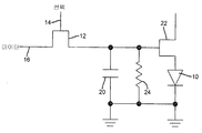
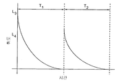
반대로, 액티브-매트릭스 회로는 디스플레이의 각각의 발광 소자에 대한 2차원 어레이의 개별 회로를 이용한다. 액티브-매트릭스 회로는 (또한 픽셀 또는 서브-픽셀로 공지되어 있는) 발광 소자를 통해 전류를 제공하기 위해 구동 회로를 제어하는데 이용되는 (전형적으로는 커패시터 상의 전하로서) 값을 저장하기 위한 제어 메커니즘을 제공한다. 여기에 사용된 바와 같이, 각각의 발광 소자는 다른 발광 소자와의 그룹화(grouping) 또는 색에 상관없이, 픽셀로 고려된다. 예를 들어, 도 12를 참조하면, LED(10)를 구동하기 위한 액티브-매트릭스 픽셀 회로는 선택 신호(14) 및 데이터 신호(16)와 같은 제어 신호에 응답하는 제어 트랜지스터(12)를 포함한다. 선택 신호(14)의 활성화에 따라, 제어 트랜지스터(12)가 켜지고 데이터 신호(16)는 저장 커패시터(20)에 전하를 제공한다. 이어서 제어 트랜지스터(12)는 선택 신호(14)의 비활성화에 의해 꺼진다. 저장 커패시터(20)상에 저장된 전하는 커패시터(20) 상에 저장된 전하에 상응하는 레벨에서 LED(10)에 전류를 제공하기 위해 구동 트랜지스터(22)를 켠다. 도 13a를 참고하면, 픽셀은 제 1 프레임 주기(T1) 동안 휘도 레벨(L1)로, 제 2 프레임 주기(T2) 동안 제 2 휘도 레벨(L2)로 광을 방출한다. 휘도에서의 변화는 이미지에서의 변화, 예를 들어 장면에서의 움직임으로 관측자에 의해 인지된다. In contrast, the active-matrix circuitry utilizes a separate circuit of a two dimensional array for each light emitting element of the display. The active-matrix circuitry has a control mechanism for storing a value (typically as a charge on a capacitor) that is used to control the drive circuit to provide current through a light emitting element (also known as a pixel or sub-pixel). to provide. As used herein, each light emitting device is considered a pixel, regardless of the grouping or color with other light emitting devices. For example, referring to FIG. 12, an active-matrix pixel circuit for driving an
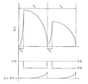
통상적인, 종래의 평-패널 디스플레이에서, 디스플레이 신호는 비디오 스트림의 다음 프레임들에서 매끄러운 움직임의 출현을 제공하기에 충분히 높은 비율로 주기적으로 리프레시된다. 리프레시율은 텔레비젼에 대해 초당 50 또는 60 프레임, 모니터에 대해 초당 30, 60, 70, 75, 80, 90, 또는 100 프레임이다. 그러므로, 통상적 평-패널 디스플레이에서, 전하 저장 커패시터(20)에서의 전하는 응용에 적당한 선택된 리프레시율로 업데이트된다. In a typical, flat panel display, the display signal is periodically refreshed at a rate high enough to provide the appearance of smooth movement in the next frames of the video stream. The refresh rate is 50 or 60 frames per second for the television and 30, 60, 70, 75, 80, 90, or 100 frames per second for the monitor. Therefore, in a typical flat-panel display, the charge in the
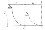
각각의 픽셀에서의 휘도 값은 프레임 주기를 정의하는 (예를 들어, 30 Hz 또는 60Hz) 리프레시율로 전형적으로 리프레시된다. 프레임 주기는 픽셀의 휘도 값이 변하는 경우 움직임의 착시가 제공되도록 충분히 짧게 선택된다. 공지된 바와 같이, 망막의 다른 부분에 이미지를 노출하며, 관측자의 눈이 디스플레이 전체에 걸쳐 이동할 수 있는 반면 프레임 주기 동안 이미지가 정적이기 때문에, 이와 같은 액티브-매트릭스 회로는 관측자에 움직임 번짐(motion blur)을 야기할 수 있다. 이 번짐은 리프레시의 주기를 감소함으로써 감소될 수 있고, 즉 더 높은 주파수에서 리프레싱 한다. 이와 같은 해결책은, 드라이버의 비용을 인상시키고 각각의 픽셀 위치에서 전하를 저장하는데 사용된 제어 라인에서 전송 라인 효과를 악화시키는, 더 높은 주파수 신호가 이용된다는, 문제점이 있다. 대안으로는, 픽셀이 광을 방출하는 각각의 프레임 동안의 시간이 예를 들어, 프레임 시간의 일부 동안만 더 밝은 광을 방출하는 것에 의해, 감소될 수 있다. 프레임 주기가 충분히 짧다면, 어떠한 플릭커도 인지되지 않을 것이다. 도 13b를 참고하면, 제 1 프레임 주기 T1 동안, 픽셀은 주기 T1의 절반 동안에 2 배의 광(2L1)을 방출하도록 제어될 수 있고, 주기 T2의 절반 동안, 2 배의 휘도 레벨(2L2)로 광을 방출하도록 마찬가지로 제어될 수 있다. 관련 해결방법에서, 디스플레이의 일부가 디스플레이 전체에 걸쳐 스크롤하는 블랙 바(black bar)를 디스플레이할 수 있다. 그러나, 이들 해결방법은 또한 비용을 인상시키는 더 높은-주파수 제어를 요구하며 더 긴 제어 라인을 가지는 더 큰 디스플레이는 문제가 있다. The luminance value at each pixel is typically refreshed at a refresh rate that defines the frame period (eg 30 Hz or 60 Hz). The frame period is chosen short enough to provide an illusion of motion when the luminance value of the pixel changes. As is known, this active-matrix circuitry exposes motion blur to the viewer because it exposes the image to other parts of the retina and the viewer's eye can move across the display while the image is static during the frame period. May cause). This bleeding can be reduced by reducing the period of refresh, ie refreshing at higher frequencies. This solution has the problem that higher frequency signals are used, which raises the cost of the driver and worsens the transmission line effect in the control line used to store the charge at each pixel location. Alternatively, the time during each frame in which the pixel emits light can be reduced, for example by emitting brighter light only during a portion of the frame time. If the frame period is short enough, no flicker will be noticed. Referring to FIG. 13B, during the first frame period T 1 , the pixel can be controlled to emit twice the light 2L 1 during half of the period T 1 , and twice the luminance level during half of the period T 2 . It can likewise be controlled to emit light at 2L 2 . In a related solution, a portion of the display may display a black bar that scrolls across the display. However, these solutions also require higher-frequency control which adds cost and larger displays with longer control lines are problematic.
공지된 펄스-폭 변조 기술은 도 13b에 설명된 바와 같이 디스플레이 픽셀을 제어하는데 이용될 수 있다. 또한, OLED 디스플레이에서의 불균일성의 하나의 근원이 액티브-매트릭스에 이용된 박막 드라이브 트랜지스터의 역치 스위칭 특성에서의 가변성에서 나온 결과이기 때문에, 액티브-매트릭스 OLED 디스플레이에서의 균일성을 개선하는 하나의 접근은 전하-축적(charge-deposition) 제어 기술과 대조하여 펄스-폭 변조 기술을 이용하는 것이다. 이들 펄스-폭 변조 기술은 제 1 특정 시간 동안 최대 전류 및 밝기로 OLED를 구동하고 이어서 동일 프레임 시간 내에서 제 2 시간의 양 동안 OLED를 끄는 것에 의해 동작한다. 제 1 시간과 제 2 시간의 양의 합이 충분히 작다면, 주기적으로 OLED를 켜고 끄는 것에서 생긴 플릭커는 시청자에서 인지되지 않을 것이다. OLED 소자의 밝기는 OLED가 꺼진 시간의 양과 비교하여 OLED가 켜지는 시간의 양의 비를 변경함으로써 제어된다. Known pulse-width modulation techniques can be used to control the display pixels as described in FIG. 13B. In addition, one approach to improving uniformity in active-matrix OLED displays is because one source of non-uniformity in OLED displays is the result of variability in the threshold switching characteristics of thin film drive transistors used in active-matrix. The pulse-width modulation technique is used in contrast to the charge-deposition control technique. These pulse-width modulation techniques operate by driving the OLED at maximum current and brightness for a first specific time and then turning off the OLED for a second amount of time within the same frame time. If the sum of the amounts of the first time and the second time is small enough, the flicker resulting from periodically turning the OLED on and off will not be perceived by the viewer. The brightness of the OLED device is controlled by changing the ratio of the amount of time the OLED is turned on compared to the amount of time the OLED is turned off.
펄스-폭 변조를 사용하는 OLED 디스플레이를 제어하는 다양한 방법이 공지되어 있다. 예를 들어, 2004년 10월 26일에 승인된 "Gray scale pixel driver for electrocinc display and method of operation therefore"란 명칭의 US 6,809,710은 그래픽 디스플레이에서 OLED를 구동하기 위한 회로를 개시하고 있다. 이 회로는 스위칭 모드에서 동작하는 OLED의 단자에 연결된 전류원을 이용한다. 전류원은 선택적으로 설정된 순환 전압 신호 및 순환 가변 진폭 전압 신호의 조합에 응답한다. 스위치-온된 경우 전류원은 최대 휘도를 달성하기 위해 OLED에 필요한 전류의 양을 OLED에 공급하도록 설계되고 최적화되어 있다. 스위치-오프된 경우, 전류원은 OLED 디스플레이에 균일한 블랙 레벨을 제공하는, OLED로 전류의 공급을 차단한다. OLED의 분명한 휘도는 OLED에 공급된 전류의 펄스 폭을 변조하여, 전류가 OLED에 공급되는 동안의 시간의 길이를 변경함으로써 제어된다. Various methods of controlling OLED displays using pulse-width modulation are known. For example, US 6,809,710, entitled “Gray scale pixel driver for electrocinc display and method of operation therefore,” approved October 26, 2004, discloses a circuit for driving an OLED in a graphic display. This circuit uses a current source connected to the terminals of the OLED operating in the switching mode. The current source is responsive to a combination of an optionally set cyclic voltage signal and a cyclic variable amplitude voltage signal. When switched on, the current source is designed and optimized to supply the OLED with the amount of current required by the OLED to achieve maximum brightness. When switched off, the current source cuts off the supply of current to the OLED, which provides a uniform black level to the OLED display. The apparent brightness of the OLED is controlled by modulating the pulse width of the current supplied to the OLED, changing the length of time while the current is supplied to the OLED.
전류원에서의 동작의 스위칭 모드를 사용함으로써, 회로는 전류-구동 OLED 디스플레이에서의 휘도 값을 제어하도록 더 큰 범위의 전압을 이용할 수 있다. 그러나, 전류-구동 회로의 사용은 복잡하며 디스플레이 장치에서 각각의 픽셀에 대한 더 큰 양의 공간을 필요로 한다. By using the switching mode of operation at the current source, the circuit can use a larger range of voltages to control the luminance value in the current-driven OLED display. However, the use of current-driven circuits is complex and requires a larger amount of space for each pixel in the display device.
또한 단일 회로에서 펄스폭 제어 및 가변 전하 축적 제어 모두를 제공하는 방법들이 공지되어 있다. "Drive circuit for active matrix light emitting device"란 명칭의 US 6,670,773은 OLED 소자와 병렬인 트랜지스터를 제안한다. 그러나, 설명된 기술은 OLED로부터 구동 전류의 방향을 바꿔, 회로의 동작 효율을 감소시킨다. 다른 설계는 OLED 소자의 성능을 제어하거나 또는 측정하기 위한 OLED 소자와 직렬인 회로 소자를 이용한다. 예를 들어, 2004년 4월 29일에 공개된, "Active Matrix Organic Electroluminecesent Display Device"란 명칭의, WO 2004/036536은 OLED 소자와 직렬인 추가 소자들을 가지는 회로를 설명하고 있다. 그러나, OLED 소자와 직렬로 위치한 경우, 트랜지스터는 OLED 소자를 구동하는데 필요한 전체 전압을 증가시키거나 또는 다른 방법으로 OLED 소자에 의해 사용된 전체 전력을 증가시키거나 또는 OLED 소자에 이용가능한 전류의 범위를 감소시킬 것이다. Also known are methods for providing both pulse width control and variable charge accumulation control in a single circuit. US 6,670,773, entitled “Drive circuit for active matrix light emitting device,” proposes a transistor in parallel with an OLED device. However, the described technique redirects the drive current from the OLED, reducing the operating efficiency of the circuit. Another design utilizes circuit devices in series with the OLED device for controlling or measuring the performance of the OLED device. For example, WO 2004/036536, published on April 29, 2004, entitled "Active Matrix Organic Electroluminecesent Display Device", describes a circuit with additional devices in series with the OLED device. However, when placed in series with an OLED device, the transistor increases the total voltage required to drive the OLED device or otherwise increases the total power used by the OLED device or changes the range of current available to the OLED device. Will reduce.
2006년 8월 8일에 발행된, Cok에 의한, 미국 특허 7,088,051에서, 가변 제어를 이용하는 펄스-폭 변조 방식이 개시되어 있고 본 발명에 참고로 그대로 통합되어 있다. 이 개시내용은 프레임 시간 동안 픽셀의 휘도를 제어하는 수단을 설명한다; 그러나, 외부 제어가 필요하며, 이에 의해 비용이 증가되고 장치의 구경비(aperture ratio)를 감소시킨다. In US Pat. No. 7,088,051 by Cok, issued August 8, 2006, a pulse-width modulation scheme using variable control is disclosed and incorporated herein by reference in its entirety. This disclosure describes means for controlling the luminance of a pixel during the frame time; However, external control is needed, thereby increasing the cost and reducing the aperture ratio of the device.
그러므로, 간단하고 유연한 구조를 가지는 액티브-매트릭스 OLED 장치용 개선된 제어 회로가 필요하다. Therefore, there is a need for an improved control circuit for active-matrix OLED devices having a simple and flexible structure.
일 실시예에 따라, 본 발명은:According to one embodiment, the invention is:
a) 프레임 주기 동안 저장 회로에 휘도값을 저장하기 위한 제어 신호에 응답하는 제어 회로;a) a control circuit responsive to a control signal for storing the luminance value in the storage circuit for a frame period;
b) 휘도값에 의해 결정된 휘도 레벨로 광을 방출하기 위해 LED를 통해 전류를 제어하기 위한 저장 회로에 응답하는 구동 회로; 및b) a drive circuit responsive to a storage circuit for controlling a current through the LED to emit light at a brightness level determined by the brightness value; And
c) 프레임 주기 동안 저장 회로에 저장된 휘도값의 감소를 제어하는 저장 회로에 연결된 휘도값 감소 회로를 포함하는, LED 디스플레이 픽셀을 제어하는 액티브-매트릭스 회로로 지향되어 있다. c) directed to an active-matrix circuit that controls the LED display pixels, including a luminance value reduction circuit coupled to the storage circuit that controls the reduction of the luminance value stored in the storage circuit during the frame period.
본 발명의 내용에 포함되어 있음.Included in the context of the present invention.
도 1은 본 발명의 구성소자를 설명하는 블록도이다;
도 2는 본 발명의 일 실시예를 설명하는 회로도이다;
도 3은 본 발명의 다른 실시예를 설명하는 회로도이다;
도 4는 본 발명의 또다른 실시예를 설명하는 회로도이다;
도 5는 본 발명의 대안의 실시예를 설명하는 회로도이다;
도 6은 본 발명의 실시예에 따른 픽셀 휘도를 설명하는 타이밍도이다;
도 7은 본 발명의 다른 실시예에 따른 픽셀 휘도를 설명하는 타이밍도이다;
도 8은 본 발명의 실시예에 따른 디지털 제어 신호를 포함하며 픽셀 휘도를 설명하는 더 상세한 타이밍도이다;
도 9은 본 발명의 실시예에 따른 디지털 제어 신호를 포함하며 픽셀 휘도를 설명하는 더 상세한 타이밍도이다;
도 10은 본 발명의 실시예에 따른 아날로그 제어 신호를 포함하며 픽셀 휘도를 설명하는 더 상세한 타이밍도이다;
도 11은 본 발명의 실시예에 따른 블록도 및 회로 소자를 설명하는 회로도이다;
도 12는 종래 기술의 액티브-매트릭스 픽셀-회로도이다;
도 13a 및 13b는 종래 기술에 공지된 제어 방법에 따른 픽셀 휘도를 설명하는 타이밍도이다;
도 14는 본 발명의 실시예에 따른 디스플레이 시스템을 설명하는 블록도이다; 그리고
도 15는 본 발명의 실시예에 따른 방법을 설명하는 흐름도이다.
본 발명은 개선된 성능을 제공하며 간소화된 제어 구조를 가지는 OLED 제어 장치를 제공한다.1 is a block diagram illustrating the components of the present invention;
2 is a circuit diagram illustrating one embodiment of the present invention;
3 is a circuit diagram illustrating another embodiment of the present invention;
4 is a circuit diagram illustrating another embodiment of the present invention;
5 is a circuit diagram illustrating an alternative embodiment of the present invention;
6 is a timing diagram illustrating pixel luminance according to an embodiment of the present invention;
7 is a timing diagram illustrating pixel brightness according to another embodiment of the present invention;
8 is a more detailed timing diagram illustrating pixel brightness, including digital control signals, in accordance with an embodiment of the present invention;
9 is a more detailed timing diagram illustrating pixel brightness, including digital control signals, in accordance with an embodiment of the present invention;
10 is a more detailed timing diagram illustrating pixel brightness, including analog control signals, in accordance with an embodiment of the present invention;
11 is a circuit diagram illustrating a block diagram and circuit elements according to an embodiment of the present invention;
12 is an active-matrix pixel-circuit diagram of the prior art;
13A and 13B are timing diagrams illustrating pixel luminance according to a control method known in the prior art;
14 is a block diagram illustrating a display system according to an embodiment of the present invention; And
15 is a flowchart illustrating a method according to an embodiment of the present invention.
The present invention provides an OLED control device that provides improved performance and has a simplified control structure.
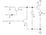
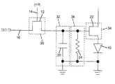
도 1을 참고하여, 본 발명의 일 실시예에 따른, LED 디스플레이 픽셀을 제어하기 위한 액티브-매트릭스 제어 회로(8)는, 프레임 주기 동안 저장 회로(32)에 휘도 값을 저장하기 위한 제어 신호(15)에 응답하는 제어 회로(30), 휘도 값에 의해 결정된 휘도 레벨에서 광을 방출하기 위해 LED(10)을 통해 전류를 제어하기 위한 저장 회로(32)에 응답하는 구동 회로(34), 및 프레임 주기 동안 저장 회로(32)에 저장된 휘도 값의 감소를 제어하는 저장 회로(32)에 연결된 휘도값-감소 회로(36)를 포함한다. 제어된 휘도값의 감소는 아날로그 또는 디지털이고 연속하거나 또는 불연속이다. 그러나, 본 발명에 이용된 바와 같이 제어된 감소는 바람직하게는 온 및 오프와 같은, 적어도 2 개의 상태를 가진다. 이와 같은 2개의 상태 제어는 본 발명에 포함되지 않은 펄스-폭 변조 방식에 이용된다. 여기서 이용된 바와 같이, 저장 회로에서의 휘도 값의 제어된 감소는 0이 아닌 제 1 값에서 제 2, 더 작은 값, 및 제 2 값보다 작은 제 3 값으로 휘도 값을 변경한다. 제 3 값은 0일 수 있지만 반드시는 아니다. Referring to FIG. 1, an active-matrix control circuit 8 for controlling an LED display pixel according to an embodiment of the present invention includes a control signal for storing a luminance value in the
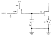
도 2를 참고하면, 본 발명의 하나의 예시적 실시예에서, 제어 회로(30) 또는 구동 회로(34)(도 1)는 예를 들어, 저온의 폴리실리콘, 결정질 실리콘, 또는 비정질 실리콘으로 형성된, 하나의 기판상에 각각 형성된, 트랜지스터(12) 또는 트랜지스터(22)로 설명된다. 저장 회로(32)는 휘도 값을 나타내는 전하를 저장하기 위한 커패시터(20)일 수 있다. 이 경우에, 휘도값 감소 회로(36)는 시간에 걸쳐 커패시터(20)에 저장된 전하를 감소시킬 수 있다. 또다른 실시예에서, 도 2에 도시된 바와 같이, 휘도-값 감소 회로(36)는 커패시터(20) 전체에 병렬로 연결된 저항기(24)이다. 비록 다른 기준 전압이 다양한 회로 소자에 이용될 수 있더라도, 도 1의 Vdd는 전압 공급원이며 회로는 접지 전압 기준으로 설명되어 있다. 도 11을 참고하면, 도 1의 소자에 관한 설명은 도 2의 소자와 함께 도시되어 있다. Referring to FIG. 2, in one exemplary embodiment of the present invention, the
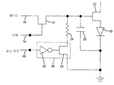
도 3에 설명된 대안의 예시적 실시예에서, 휘도-값 감소 회로(36)는 커패시터(20)에서의 전하가 시간에 걸쳐 감소하는 비율을 제어하기 위해 감소-제어 신호(40)에 응답하며 커패시터(20) 전체에 병렬로 연결된 트랜지스터(26)이다.In the alternative exemplary embodiment described in FIG. 3, the luminance-
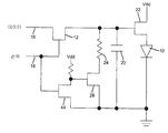
도 4에 설명된 본 발명의 또다른 예시적 실시예에서, 감소-제어 신호(40)에 응답하는 감소-제어 회로(38)는 휘도 값 감소 회로(36)가 휘도 값을 감소시키는 비율을 제어하기 위해 휘도-값 감소 회로(36)에 연결되어 있다. 도 4에 도시된 바와 같이, 감소-제어 회로(38)는 감소-제어 신호(40)에 응답하여 저항기(24)를 통해 전류의 흐름을 제어하기 위해 (휘도값 감소 회로(36)를 포함하는) 저항기(24)와 직렬로 감소-제어 트랜지스터(28)를 포함한다. 감소-제어 신호(40)는 (도시되지 않은) 감소-제어 트랜지스터(28)를 직접 제어할 수 있거나 또는 감소-제어 신호(40)는 선택 신호(14)가 활성되지 않는 경우 휘도 값이 감소만 되도록 인버터(42)를 통해 (점선으로 도시된) 선택 신호(14)로부터 유도될 수 있다. 도 5를 참고하면, 이와 같은 인버터(42)는 반전 트랜지스터(44)를 포함할 수 있다. 그러므로, 외부 제어는 도 2 및 도 5에 도시된 바와 같이, 제어된 휘도 값 감소가 발생할 필요가 없다. In another exemplary embodiment of the invention described in FIG. 4, the reduction-
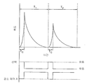
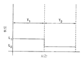
동작에서, 픽셀 회로는 도 12를 참고로 하여 설명된 바와 같이 저장 회로에 전하를 저장한다. 커패시터(20)가 충전되는 경우, 구동 트랜지스터(22)는 캐소드 접지 전압으로 구동 트랜지스터(22)와 LED(10)을 통해, 전력 신호(Vdd)로부터의 전휴 흐름을 제공하도록 비례하여 켜지며, 이에 의해 LED가 커패시터(16) 상의 전하에 대응하는 광의 양을 방출하게 한다. 본 발명에 따르면, 그러나, 휘도 값이 저장 회로에 저장되고 구동 회로가 LED가 광을 방출하게 한다면, 휘도 값은 예를 들어 (도 2에 도시된 바와 같이) 저항 또는 (도 3에 도시된 바와 같이) 트랜지스터를 통해 방전함으로써 감소된다. 방전이 일어나는 비율은 (도 2에 도시된 바와 같이) 저항 및 커패시터 값의 선택 또는 (도 3에 도시된 바와 같이) 이용된 제어 메커니즘에 좌우된다. 방전은 연속적이고 지수적일 수 있거나 또는 약간 다른 감소 곡선을 가질 수 있다. 도 6을 참고하면, 결과는 LED의 휘도가 휘도 레벨(L3)로부터 0으로 리프레시 주기(T1) 내에서 시간에 걸쳐 감소된다; 그리고 제 2 리프레시 주기(T2)에서 휘도 레벨 (L4)로부터 0으로 감소된다. (도 13a에 도시된 바와 같이) 종래 기술의 액티브-매트릭스 회로와 명백하게 유사한 밝기를 유지하기 위해, 휘도 곡선 아래의 영역이 바람직하게는 동일해야 함을 유의한다. LED 장치의 평균 밝기는 리프레시 주기 동안 방출된 광의 전체 양으로 감지된다. 그러므로, T2가 도 13b에서 인것처럼, L3은 L1보다 클 것이다. 도 6에 도시된 바와 같이, 휘도 값의 제어된 감소는 축적 사이클이 완료하자마자, 즉 선택 신호가 불활성화된 경우, 실질적 지연 없이, 시작한다. 실질적 지연 없이란 선택 신호가 불활성된 경우 제어된 감소가 시작하고, 임의 제어 신호(40)가 있다면, 활성됨을 의미한다. In operation, the pixel circuit stores charge in the storage circuit as described with reference to FIG. When the
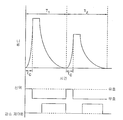
도 7에 도시된 바와 같이, 저장 회로에 전하를 축적하기 위해 픽셀 회로의 선택과 비교하여 휘도 감소의 타이밍을 제어하기 위해 외부 감소-제어 신호(40)를 이용함으로써, 휘도 방출의 프로파일은 예를 들어 리프레시 주기(Ts)의 일부에 대해 임의 휘도 감소를 방지하는 것에 의해, 제어된다. 전술한 바와 같이, 일정한 휘도 인식을 유지하기 위해, 곡선 아래의 전체 영역은 바람직하게는 일정해야 한다. 그러므로, (제 1 리프레시 주기(T1) 동안) L5의 초기 휘도 레벨은 L3보다 낮고 L6의 초기 휘도 레벨은 (제 2 리프레시 주기(T2) 동안) L4 보다 낮다. 이 경우에, 휘도 값의 제어된 감소는 선택 신호의 불활성 이후 어느 정도까지 지연된다.As shown in FIG. 7, by using an external reduction-
도 6 및 7에 관한 설명은 저장 회로에 휘도 값을 저장하는데 요구된 리프레시 주기에서 사간을 포함하지 않는다. 저장 회로가 전형적으로 전하를 저장하는 커패시터이지만, 필연적이지 않기 때문에, 임의 방전 메커니즘(예를 들어, 저항)은 레지스터로부터의 임피던스 증가 및 이에 의한 전송 라인 손실 때문에 전하가 저장되는 속도를 감소시킬 수 있다. 그러므로, 리프레시 주기의 전하 저장 일부 동안 불활성되는 트랜지스터를 이용함으로써, 이와 같은 전송 라인 손실이 감소되거나 또는 예방될 수 있어, 이에 의해 휘도 값이 각각의 픽셀 회로에 저장되는 비율을 개선시킨다. 6 and 7 do not include time in the refresh period required to store the luminance value in the storage circuit. Although the storage circuit is typically a capacitor that stores charge, but not necessarily, any discharge mechanism (eg, a resistor) may reduce the rate at which charge is stored due to an increase in impedance from the resistor and thereby transmission line loss. . Therefore, by using transistors that are inactive during some of the charge storage of the refresh period, such transmission line losses can be reduced or prevented, thereby improving the rate at which the luminance values are stored in each pixel circuit.
도 8을 참고로 하면, 전하는 리프레시 주기(T1 또는 T2)의 Tc 부분 동안 저장 회로에 저장된다. Tc 부분은 설명된 선택 신호 라인으로 설명된 바와 같이 선택 신호 유효 상태에 대응한다. 감소 제어 신호(A)는 감소-제어 신호의 대응하는 반전 타이밍을 나타낸다. 예를 들어, 더 복잡한 제어가 요구된다면, 도 9의 감소-제어 타이밍(B)이 휘도 감소를 지연시킴으로써 이용될 수 있다. 도 8 및 9 모두는 디지털 감소-제어 신호를 이용한다. 그러나, 도 10 에 도시된 바와 같이, 본 발명은 또한 아날로그 제어를 이용할 수 있다. 휘도 값 감소 과정을 제어함으로써, 다양한 휘도-감소 프로파일을 달성한다. Referring to FIG. 8, the charge is stored in the storage circuit during the Tc portion of the refresh period T 1 or T 2 . The Tc portion corresponds to the selection signal valid state as described by the selection signal line described. The reduction control signal A represents the corresponding inversion timing of the reduction-control signal. For example, if more complex control is desired, the reduction-control timing B of FIG. 9 can be used by delaying the luminance reduction. 8 and 9 both use digital reduce-control signals. However, as shown in Fig. 10, the present invention can also use analog control. By controlling the luminance value reduction process, various luminance-reduction profiles are achieved.
본 발명의 다양한 실시예에 따르면, (직렬 소자가 LED를 구동하는데 필요한 전압(Vdd)을 증가시켜, 이에 의해 시스템의 효율성을 감소시키는) LED 소자 자체와 직렬인 제어 트랜지스터, 또는 (병렬 소자가 전류의 방향을 바꿔, 시스템의 효율성을 감소시키는) LED와 병렬인 전류-전환 트랜지스터가 요구되지 않는 반면, 여전히 단일 주기 내에서 감소하는 휘도 레벨로 액티브-매트릭스 LED 소자를 구동하기 위한 수단을 제공한다. According to various embodiments of the present invention, a control transistor in series with the LED element itself (which increases the voltage Vdd necessary for the serial element to drive the LED, thereby reducing the efficiency of the system), or the parallel element is a current While current-switching transistors in parallel with the LEDs are not required, which reverses the direction, reducing the efficiency of the system, it still provides a means for driving the active-matrix LED elements with decreasing brightness levels within a single period.
공지된 바와 같이, 종래 기술의 액티브 매트릭스 OLED 디스플레이 장치에서 찾을 수 있는 것과 같은 축적-및-유지(deposit-and-hold) 회로는, 관찰자의 눈이 디스플레이 장치 스크린 전체에서 움직이는 물체를 추적하려 한다면, 지각적 번짐을 가져올 수 있다. OLED가 발광하는 시간의 길이를 감소시키기 위해 저장 회로에서 휘도 값을 조절함으로써, 이 번짐 영향은 감소될 수 있다. 본 발명에 따른 픽셀에 의한 휘도 출력이 통상적인 액티브-매트릭스 제어 방식에서 트루(true)인 것보다 더 빠르게 쇠퇴하기 때문에, 관측자의 눈이 시야를 가로질러 이동하는 반면 시간에 걸쳐 일정 휘도를 유지하는 번짐 영향이 감소된다. 본 발명은 이와 같은 디스플레이 장치에서 움직임 잡음(motion artifact)을 더 간단히 감소시키는데 이용될 수 있다. As is known, deposit-and-hold circuits such as those found in active matrix OLED display devices of the prior art, if the observer's eye is to track a moving object across the display device screen, Perceptual bleeding can result. By adjusting the luminance value in the storage circuit to reduce the length of time that the OLED emits light, this bleeding effect can be reduced. Since the luminance output by the pixel according to the invention decays faster than true in conventional active-matrix control schemes, the observer's eye moves across the field of view while maintaining a constant luminance over time. Smear effect is reduced. The present invention can be used to more simply reduce motion artifacts in such display devices.
평-패널 디스플레이에서, 기판상에 형성된 트랜지스터는 가변 성능, 특히 가변 역치 전압을 가질 수 있음의 공지되어 있다. 본 발명은 리프레시 주기의 일부 동안(예를 들어, Ts), 구동 트랜지스터가 포화된 구동 상태에 있을 수 있다는 추가 이점을 가진다. 이와 같은 포화 상태(트랜지스터가 동작할 수 있는 최대)는 전형적으로 제조 가변성을 덜 겪으므로, 디스플레이는 리프레시 사이클의 이 일부 동안 더 균일한 외관(appearance)을 제공한다. 그러므로, 본 발명의 추가 실시예에서, 구동 트랜지스터는 저장 회로의 휘도 값에 응답하여, 리프레시 사이클의 전부가 아닌, 일부 동안 포화된 상태에 있다. In flat-panel displays, it is known that transistors formed on substrates can have variable performance, in particular variable threshold voltages. The present invention has the additional advantage that during some of the refresh periods (eg, Ts), the drive transistors may be in a saturated drive state. Since this saturation (the maximum at which the transistor can operate) typically suffers from less manufacturing variability, the display provides a more uniform appearance during this part of the refresh cycle. Therefore, in a further embodiment of the present invention, the drive transistor is in a saturated state for some, but not all of the refresh cycle, in response to the luminance value of the storage circuit.
종래 기술의 전형적 펄스-폭 변조 방식에서, LED는 주기의 데이터-의존 가변 부분 동안 일정한, 높은 밝기로 구동된다. 이 방식에서, 데이터는 LED를 다시 온 및 오프 하기 위해, 매 주기에 적어도 2번 기록된다. 이 방식은 또한 재료의 수명을 감소시키는, 큰 LED 구동 전류가 사용될 수 있고, 복잡한 매우 높은-비율의 제어 신호가 가변 펄스 폭을 제어하는데 이용될 수 있음을 요구한다. 가변 펄스 폭은 8-비트 그레이-스케일 디스플레이를 지원하기 위해 주기의 적어도 1/256 내에서 제어된다. 이는 수행하기 어려울 수 있다. 그러므로, 본 발명의 또다른 이점은 간소화된 제어이다. 예를 들어, 데이터는 오직 한번 기록될 수 있다. In typical pulse-width modulation schemes of the prior art, LEDs are driven at a constant, high brightness during the data-dependent variable portion of the period. In this manner, data is written at least twice in every cycle, to turn the LED back on and off. This approach also requires that large LED drive currents, which reduce the life of the material, can be used and complex very high-ratio control signals can be used to control the variable pulse width. The variable pulse width is controlled within at least 1/256 of the period to support 8-bit gray-scale display. This can be difficult to perform. Therefore, another advantage of the present invention is the simplified control. For example, data can only be written once.
본 발명은 또한 OLED 소자의 동작 특성에서의 변화를 보상하는데 이용될 수 있다. OLED를 사용하는 경우, 이들의 효율성이 떨어지며 저항은 증가한다. 리프레시 주기의 제 2 부분에 대하여 리프레시 주기의 제 1 부분 내의 휘도 감소를 제어하는 것에 의해, 더 많은 광은 장치에 의해 방출되며, 이에 의해 OLED 소자의 감소된 광 출력 효율성을 보상한다. 그러므로, 본 발명의 또다른 예시적 실시예에서, 감소-제어 신호는 OLED 물질 노화를 보상하는데 이용된다. 또한 리프레시 주기에서 픽셀로부터 방출된 광의 전체 양을 변경하기 위해 감소 제어 신호를 개별적으로 조절함으로써 균일성 변화를 보상하는데 이용될 수 있다. The present invention can also be used to compensate for changes in operating characteristics of OLED devices. When using OLEDs, their efficiency decreases and resistance increases. By controlling the reduction in luminance in the first portion of the refresh period relative to the second portion of the refresh period, more light is emitted by the device, thereby compensating for the reduced light output efficiency of the OLED element. Therefore, in another exemplary embodiment of the present invention, a decrease-control signal is used to compensate for OLED material aging. It can also be used to compensate for the uniformity change by individually adjusting the reduction control signal to change the total amount of light emitted from the pixel in the refresh period.
도 14를 참고하면, 본 발명은 광을 방출하기 위해 전류에 응답하는 발광 소자를 각각 포함하는, 몇 개의 발광 픽셀(108) 및, (예를 들어, 도 1에 대응하는) 발광 소자를 제어하기 위해 대응하는 액티브-매트릭스 픽셀-구동 회로를 가지는 디스플레이(100)에 이용될 수 있다. 이들 발광 픽셀(108)은 행 및 열로 조직되고, 이에 공급된 제어 신호는 한번에 몇 개의 행 또는 열을 구동한다. 각각의 픽셀-구동 회로는 저장 회로에서 휘도 값을 저장하기 위한 제어 신호에 응답하는 제어 회로를 포함할 수 있다. 또한 휘도 값에 의해 결정된 휘도 레벨로 광을 방출하기 위해 LED를 통해 전류를 제어하기 위한 저장 회로에 응답하는 구동 회로가 포함된다. 추가로, 휘도 값 감소 회로는 시간에 걸쳐 저장 회로에 저장된 휘도 값을 감소하기 위한 저장 회로에 연결된다. 디스플레이(100)는 입력 신호(104)에 응답하는 제어기(102)에 의해 제공된 (전력 및 제어 신호를 포함하는) 신호(106)로 구동될 수 있다. Referring to FIG. 14, the present invention relates to controlling several
감소-제어 신호는 공통으로 모든 LED 소자에 연결될 수 있어, 신호 제어 구조는 모든 변조 회로소자를 동작한다. 대안으로는, 개별 감소-제어 신호는 OLED의 그룹에 이용된다. 예를 들어, 이들 그룹은 컬러 디스플레이에서 특정 색의 광을 방출하는 모든 LED 소자를 포함할 수 있다. 다른 LED 물질이 다른 색을 방출하기 위해 컬러 디스플레이에 이용되고 다른 비율로 노화하기 때문에, 각각의 LED 색-소자 그룹화(grouping)를 개별적으로 제어하는 것이 유리할 수 있다. 전형적으로는, 데이터 및 선택 제어 신호들은 한번에 디스플레이에서 라인들 또는 열들을 리프레시 한다. 행 또는 열을 통한 동일한 사이클링 방법이 변조 신호를 제어하도록 이용될 수 있어, 변조 신호에 공통으로 연결된 각각의 LED가 한 번에 하나의 열 또는 행으로 업데이트될 것이며, LED가 동일한 시간 동안 광을 방출하게 한다. The reduction-control signal can be commonly connected to all LED elements, such that the signal control structure operates all modulation circuitry. Alternatively, separate reduction-control signals are used for groups of OLEDs. For example, these groups may include all LED devices that emit light of a particular color in a color display. Since different LED materials are used in color displays to emit different colors and age at different rates, it may be advantageous to individually control each LED color-device grouping. Typically, data and selection control signals refresh lines or columns in the display at one time. The same cycling method through rows or columns can be used to control the modulation signal so that each LED commonly connected to the modulation signal will be updated to one column or row at a time and the LEDs emit light for the same time Let's do it.
본 발명의 사용에 적합한 LED 제어기는 통상적 디지털 논리 제어 방법을 사용하여 구성될 수 있다. 회로 제어 신호는 통상적 설계를 사용하여 적용될 수 있다. 도 15를 참고하면, 이와 같은 제어기는 단계 200에서 휘도 값에 의해 결정된 휘도 레벨로 광을 방출하기 위해 LED를 통해 전류를 제어하도록 저장 회로의 휘도 값을 저장하고, 단계 202에서 저장 회로에 저장된 휘도 값을 감소시키기 위해 저장 회로에 연결된 휘도값 감소 회로를 이용함으로써 프레임 주기 내에서 휘도 값의 감소를 제어하기 위해, LED 픽셀 제어 신호를 이용함으로써 프레임 주기 내에서 디스플레이 장치의 휘도를 감소시키는 방법을 이행한다. LED controllers suitable for use in the present invention may be configured using conventional digital logic control methods. Circuit control signals can be applied using conventional designs. Referring to FIG. 15, such a controller stores the brightness value of the storage circuit to control the current through the LED to emit light at the brightness level determined by the brightness value in
바람직한 실시예에서, 본 발명은 "Electroluminescent Device with Modified Thin Film Luminescent Zone"란 명칭의 Tang 등에 의한, 1988년 9월 6일에 발행된, 미국 특허 제 4,769,292호 및 "Electroluminescent Device with Organic Electroluminescent Medium"란 명칭의, VanSlyke 등에 의한 1991년 10월 29일에 발행된, 미국 특허 제 5,061,569호에 개시되어 있으나, 이에 제한되지 않는 소분자 또는 고분자 OLED로 구성된 유기 발광 다이오드(OLED)를 포함하는 방출 디스플레이에 이용된다. OLED 물질 및 구조의 많은 조합 및 변경이 당해 기술에 공지될 수 있는 것에 이용가능하며, 본 발명에 따른 OLED 디스플레이 장치를 제조하는데 사용될 수 있다. 대안의 실시예에서, 본 발명은 유기 발광 물질, 예를 들어, 다결정 반도체 매트릭스 내의 양자점 또는 인광성 결정을 가지고 이용된다. In a preferred embodiment, the invention relates to U.S. Patent No. 4,769,292 and "Electroluminescent Device with Organic Electroluminescent Medium," issued September 6, 1988, by Tang et al., Entitled "Electroluminescent Device with Modified Thin Film Luminescent Zone." Used in emission displays comprising organic light emitting diodes (OLEDs) consisting of small molecule or polymer OLEDs, which are disclosed in U.S. Pat.No. 5,061,569, issued October 29, 1991 to VanSlyke et al. . Many combinations and modifications of OLED materials and structures are available to those known in the art and can be used to make OLED display devices in accordance with the present invention. In an alternative embodiment, the invention is used with organic luminescent materials, for example quantum dots or phosphorescent crystals in a polycrystalline semiconductor matrix.
8 액티브-매트릭스 제어 회로
10 발광 다이오드
12 제어 트랜지스터
14 선택 신호
15 제어 신호들
16 데이터 신호
20 커패시터
22 구동 트랜지스터
24 저항기
26 휘도-값-감소 트랜지스터
28 감소-제어 트랜지스터
30 제어 회로
32 저장 회로
34 구동 회로
36 휘도-값-감소 회로
38 감소-제어 회로
40 감소-제어 신호
42 인버터
44 인버터 트랜지스터
100 디스플레이
102 제어기
104 신호
106 신호
108 발광 소자
200 휘도값 저장 단계
202 휘도값 감소 단계8 active-matrix control circuit
10 light emitting diode
12 control transistor
14 selection signal
15 Control Signals
16 data signals
20 capacitors
22 driving transistor
24 resistor
26 Luminance-Value-Reducing Transistors
28 reduction-control transistors
30 control circuit
32 storage circuit
34 driving circuit
36 Luminance-Value-Reduction Circuit
38 reduction-control circuits
40 reduction-control signals
42 inverter
44 inverter transistor
100 display
102 controller
104 signals
106 signals
108 light emitting element
200 brightness value storage step
202 Decrease luminance value
Claims (20)
b) 휘도값에 의해 결정된 휘도 레벨로 광을 방출하기 위해 LED를 통해 전류를 제어하기 위한 저장 회로에 응답하는 구동 회로; 및
c) 프레임 주기 동안 저장 회로에 저장된 휘도값의 감소를 제어하는 저장 회로에 연결된 휘도값 감소 회로를 포함하는 LED 디스플레이 픽셀을 제어하는 액티브-매트릭스 회로.a) a control circuit responsive to a control signal for storing the luminance value in the storage circuit for a frame period;
b) a drive circuit responsive to a storage circuit for controlling a current through the LED to emit light at a brightness level determined by the brightness value; And
c) an active-matrix circuit for controlling the LED display pixel comprising a luminance value reduction circuit coupled to the storage circuit for controlling the reduction of the luminance value stored in the storage circuit during the frame period.
제어 회로 또는 구동 회로는 하나의 기판 상에 형성된 트랜지스터인 LED 디스플레이 픽셀을 제어하는 액티브-매트릭스 회로. The method of claim 1,
An active-matrix circuit for controlling an LED display pixel, wherein the control circuit or drive circuit is a transistor formed on one substrate.
저장 회로는 휘도값을 나타내는 전하를 저장하기 위한 커패시터인 LED 디스플레이 픽셀을 제어하는 액티브-매트릭스 회로.The method of claim 1,
The storage circuit is an active-matrix circuit that controls an LED display pixel which is a capacitor for storing a charge representing a luminance value.
휘도값 감소 회로는 시간에 걸쳐 커패시터에 저장된 전하를 감소시키는 LED 디스플레이 픽셀을 제어하는 액티브-매트릭스 회로.The method of claim 3, wherein
The luminance reduction circuit is an active-matrix circuit that controls the LED display pixels to reduce the charge stored in the capacitor over time.
휘도값 감소 회로는 커패시터 전체에 병렬로 연결된 저항인 LED 디스플레이 픽셀을 제어하는 액티브-매트릭스 회로.The method of claim 4, wherein
A luminance reduction circuit is an active-matrix circuit that controls an LED display pixel, a resistor connected in parallel across a capacitor.
휘도값 감소 회로는 커패시터 전체에 병렬로 연결된 트랜지스터이고 커패시터에서의 전하가 시간에 걸쳐 감소하는 비율을 제어하기 위해 제어 신호에 응답하는 LED 디스플레이 픽셀을 제어하는 액티브-매트릭스 회로.The method of claim 4, wherein
A luminance reduction circuit is an active-matrix circuit that controls a LED display pixel in response to a control signal to control the rate at which the charge at the capacitor decreases over time in a transistor connected in parallel across the capacitor.
휘도값 감소 회로가 휘도값을 감소시키는 비율을 제어하도록 휘도-값 감소 회로에 연결된 감소-제어 신호에 응답하는 감소-제어 회로를 더 포함하는 LED 디스플레이 픽셀을 제어하는 액티브-매트릭스 회로.The method of claim 1,
And a reduction-control circuit responsive to a decrease-control signal coupled to the brightness-value reduction circuit to control the rate at which the brightness value reduction circuit reduces the brightness value.
감소-제어 회로가 트랜지스터인 LED 디스플레이 픽셀을 제어하는 액티브-매트릭스 회로.The method of claim 7, wherein
An active-matrix circuit that controls an LED display pixel wherein the reduction-control circuit is a transistor.
저장 회로는 휘도값을 나타내는 전하를 저장하기 위한 커패시터이고, 휘도값 감소 회로는 커패시터 전체에 병렬로 연결된 저항이며, 감소-회로 트랜지스터는 감소-제어 신호에 응답하여 저항을 통해 전류의 흐름을 제어하기 위해 저항과 직렬로 연결되어 있는 LED 디스플레이 픽셀을 제어하는 액티브-매트릭스 회로.The method of claim 8,
The storage circuit is a capacitor for storing charge representing the luminance value, the luminance reduction circuit is a resistor connected in parallel across the capacitor, and the reduction-circuit transistor controls the flow of current through the resistance in response to the reduction-control signal. Active-matrix circuitry to control LED display pixels in series with resistors.
제어 신호는 제어 회로를 제어하기 위한 선택 신호를 포함하고 감소-제어 신호는 선택 신호의 반전 신호인 LED 디스플레이 픽셀을 제어하는 액티브-매트릭스 회로.The method of claim 7, wherein
The control signal comprises a selection signal for controlling the control circuit and the reduction-control signal is an active-matrix circuit for controlling the LED display pixel which is an inversion signal of the selection signal.
감소-제어 회로는 인버터인 LED 디스플레이 픽셀을 제어하는 액티브-매트릭스 회로.The method of claim 10,
Reduction-control circuitry is an active-matrix circuit for controlling LED display pixels that are inverters.
인버터는 트랜지스터인 LED 디스플레이 픽셀을 제어하는 액티브-매트릭스 회로.The method of claim 11,
An inverter is an active-matrix circuit that controls an LED display pixel, which is a transistor.
제어된 감소는 실질적 지연 없이, 휘도값이 저장 회로에 저장된 후 시작하는 LED 디스플레이 픽셀을 제어하는 액티브-매트릭스 회로.The method of claim 1,
The controlled reduction is an active-matrix circuit that controls the LED display pixels starting after the luminance value is stored in the storage circuit without substantial delay.
휘도값은 휘도값이 저장 회로에 저장된 후 프레임 주기보다 적은 제 1 주기 동안 일정한 값으로 유지되고 이후 제 1 주기의 끝에서 감소되는 LED 디스플레이 픽셀을 제어하는 액티브-매트릭스 회로. The method of claim 1,
The luminance-matrix circuitry controls the LED display pixel at which the luminance value is held constant for a first period less than the frame period after the luminance value is stored in the storage circuit and then decreased at the end of the first period.
휘도값이 저장 회로에 저장된 후 휘도값은 연속적으로 감소하는 LED 디스플레이 픽셀을 제어하는 액티브-매트릭스 회로.The method of claim 1,
An active-matrix circuit for controlling LED display pixels in which the luminance value is continuously decreased after the luminance value is stored in the storage circuit.
ⅰ) 저장 회로에 휘도값을 저장하기 위한 제어 신호에 응답하는 제어 회로;
ⅱ) 휘도 값에 의해 결정된 휘도 레벨로 광을 방출하기 위해 LED를 통해 전류를 제어하기 위한 저장 회로에 응답하는 구동 회로; 및
ⅲ) 시간에 걸쳐 저장 회로에 저장된 휘도 값을 감소시키는 저장 회로에 연결된 휘도-값 감소 회로를 더 포함하는 디스플레이 장치.A plurality of light emitting pixels formed on one substrate, each pixel driving circuit comprising a LED responsive to a current to emit light and a pixel-drive circuit for providing current to the LED, each pixel driving circuit comprising:
Iii) a control circuit responsive to a control signal for storing the luminance value in the storage circuit;
Ii) a drive circuit responsive to a storage circuit for controlling the current through the LED to emit light at a brightness level determined by the brightness value; And
Iii) a luminance-value reduction circuit coupled to the storage circuit for reducing the luminance value stored in the storage circuit over time.
LED는 유기 발광 다이오드인 디스플레이 장치.17. The method of claim 16,
LED is an organic light emitting diode display device.
LED는 무기 발광 다이오드인 디스플레이 장치. 17. The method of claim 16,
LED is an inorganic light emitting diode display device.
무기 LED는 다결정 반도체 매트릭스에서의 양자점인 디스플레이 장치.The method of claim 18,
Inorganic LEDs are quantum dots in a polycrystalline semiconductor matrix.
b) 저장 회로에 저장된 휘도 값을 감소시키기 위해 저장 회로에 연결된 휘도-값 감소 회로를 이용함으로써 프레임 주기 내에서 휘도값의 감소를 제어하는 단계를 포함하는 프레임 주기 내의 디스플레이 장치의 휘도 감소 방법.a) using the LED pixel control circuit to store the luminance value in the storage circuit to control the current through the LED to emit light at the luminance level determined by the luminance value; And
b) controlling the reduction of the luminance value within the frame period by using the luminance-value reduction circuit connected to the storage circuit to reduce the luminance value stored in the storage circuit.
Applications Claiming Priority (2)
| Application Number | Priority Date | Filing Date | Title |
|---|---|---|---|
| US11/934,152 US8120555B2 (en) | 2007-11-02 | 2007-11-02 | LED display with control circuit |
| US11/934,152 | 2007-11-02 |
Publications (1)
| Publication Number | Publication Date |
|---|---|
| KR20100095552A true KR20100095552A (en) | 2010-08-31 |
Family
ID=40544701
Family Applications (1)
| Application Number | Title | Priority Date | Filing Date |
|---|---|---|---|
| KR1020107012169A KR20100095552A (en) | 2007-11-02 | 2008-11-03 | Led display with control circuit |
Country Status (6)
| Country | Link |
|---|---|
| US (1) | US8120555B2 (en) |
| EP (1) | EP2215621A2 (en) |
| JP (2) | JP5351169B2 (en) |
| KR (1) | KR20100095552A (en) |
| CN (1) | CN101884061B (en) |
| WO (1) | WO2009058393A2 (en) |
Cited By (2)
| Publication number | Priority date | Publication date | Assignee | Title |
|---|---|---|---|---|
| KR101531542B1 (en) * | 2008-01-15 | 2015-06-25 | 가부시키가이샤 한도오따이 에네루기 켄큐쇼 | Display device and electronic appliance |
| KR20180114816A (en) * | 2017-04-11 | 2018-10-19 | 삼성전자주식회사 | A pixel circuit of a display panel and a display apparatus |
Families Citing this family (37)
| Publication number | Priority date | Publication date | Assignee | Title |
|---|---|---|---|---|
| US20090135205A1 (en) * | 2007-11-27 | 2009-05-28 | Himax Display, Inc. | Display method for color sequential display |
| US20100149163A1 (en) * | 2008-08-08 | 2010-06-17 | Oqo, Inc. | Use of spatial high-pass filtering of images to increase perceived brightness of emissive display |
| US8643283B2 (en) * | 2008-11-30 | 2014-02-04 | Cree, Inc. | Electronic device including circuitry comprising open failure-susceptible components, and open failure-actuated anti-fuse pathway |
| US9781803B2 (en) * | 2008-11-30 | 2017-10-03 | Cree, Inc. | LED thermal management system and method |
| US20110069049A1 (en) * | 2009-09-23 | 2011-03-24 | Open Labs, Inc. | Organic led control surface display circuitry |
| DE102010009442A1 (en) * | 2010-02-23 | 2011-08-25 | Siemens Aktiengesellschaft, 80333 | Symbol Gazette |
| CN103280187B (en) * | 2013-06-09 | 2015-12-23 | 上海和辉光电有限公司 | Pixel list view method, device and OLED display |
| US10839734B2 (en) * | 2013-12-23 | 2020-11-17 | Universal Display Corporation | OLED color tuning by driving mode variation |
| US10916218B2 (en) * | 2016-06-30 | 2021-02-09 | Lg Display Co., Ltd. | Organic light emitting diode display |
| EP3389037B1 (en) * | 2017-04-11 | 2020-12-09 | Samsung Electronics Co., Ltd. | Pixel circuit of display panel |
| US10629153B2 (en) * | 2017-10-13 | 2020-04-21 | Jasper Display Corp. | Backplane suitable to form part of an emissive pixel array and system and methods of modulating same |
| US11030942B2 (en) * | 2017-10-13 | 2021-06-08 | Jasper Display Corporation | Backplane adaptable to drive emissive pixel arrays of differing pitches |
| CN110556072A (en) * | 2018-05-31 | 2019-12-10 | 三星电子株式会社 | Display panel and driving method of display panel |
| KR102498084B1 (en) * | 2018-06-01 | 2023-02-10 | 삼성전자주식회사 | Display panel |
| CN110634433A (en) | 2018-06-01 | 2019-12-31 | 三星电子株式会社 | Display panel |
| JP6694989B2 (en) | 2018-06-27 | 2020-05-20 | シャープ株式会社 | Light emitting device, display device, and LED display device |
| US10951875B2 (en) | 2018-07-03 | 2021-03-16 | Raxium, Inc. | Display processing circuitry |
| TWI683434B (en) * | 2018-09-21 | 2020-01-21 | 友達光電股份有限公司 | Pixel structure |
| KR102538484B1 (en) | 2018-10-04 | 2023-06-01 | 삼성전자주식회사 | Display panel and driving method of the display panel |
| KR102538488B1 (en) | 2018-10-04 | 2023-06-01 | 삼성전자주식회사 | Display panel and driving method of the display panel |
| DE102018128847A1 (en) * | 2018-11-16 | 2020-05-20 | Osram Opto Semiconductors Gmbh | Optoelectronic lighting device and method for controlling an optoelectronic lighting device |
| CN111445843B (en) * | 2019-01-17 | 2021-05-04 | 米彩股份有限公司 | Display driving module and driving method |
| US11710445B2 (en) | 2019-01-24 | 2023-07-25 | Google Llc | Backplane configurations and operations |
| KR102583109B1 (en) * | 2019-02-20 | 2023-09-27 | 삼성전자주식회사 | Display panel and driving method of the display panel |
| US11637219B2 (en) | 2019-04-12 | 2023-04-25 | Google Llc | Monolithic integration of different light emitting structures on a same substrate |
| US11238782B2 (en) | 2019-06-28 | 2022-02-01 | Jasper Display Corp. | Backplane for an array of emissive elements |
| CN113053304A (en) * | 2019-12-26 | 2021-06-29 | 天马日本株式会社 | Pixel circuit for controlling light emitting element |
| US11626062B2 (en) | 2020-02-18 | 2023-04-11 | Google Llc | System and method for modulating an array of emissive elements |
| CN111243521B (en) * | 2020-03-31 | 2021-04-30 | 厦门天马微电子有限公司 | Pixel driving circuit, driving method and display panel |
| CN111369935B (en) * | 2020-04-09 | 2021-03-16 | 深圳市华星光电半导体显示技术有限公司 | Pixel driving circuit and driving method thereof |
| US11538431B2 (en) | 2020-06-29 | 2022-12-27 | Google Llc | Larger backplane suitable for high speed applications |
| US11282439B2 (en) * | 2020-07-16 | 2022-03-22 | X Display Company Technology Limited | Analog pulse-width-modulation control circuits |
| CN112116899A (en) * | 2020-10-12 | 2020-12-22 | 北京集创北方科技股份有限公司 | Driving device and electronic apparatus |
| US11743989B2 (en) | 2020-12-15 | 2023-08-29 | Lumileds Llc | Voltage supply amplitude modulation driving outlier microLEDs |
| US11343888B1 (en) | 2020-12-15 | 2022-05-24 | Lumileds Llc | MicroLED power considering outlier pixel dynamic resistance |
| US11191141B1 (en) | 2020-12-17 | 2021-11-30 | Lumileds Llc | Powering microLEDs considering outlier pixels |
| CN117769738A (en) | 2021-07-14 | 2024-03-26 | 谷歌有限责任公司 | Backboard and method for pulse width modulation |
Family Cites Families (25)
| Publication number | Priority date | Publication date | Assignee | Title |
|---|---|---|---|---|
| JPH08241057A (en) * | 1995-03-03 | 1996-09-17 | Tdk Corp | Image display device |
| JP3686769B2 (en) * | 1999-01-29 | 2005-08-24 | 日本電気株式会社 | Organic EL element driving apparatus and driving method |
| JP4092857B2 (en) * | 1999-06-17 | 2008-05-28 | ソニー株式会社 | Image display device |
| US6392617B1 (en) * | 1999-10-27 | 2002-05-21 | Agilent Technologies, Inc. | Active matrix light emitting diode display |
| JP2001183996A (en) | 1999-12-22 | 2001-07-06 | Tdk Corp | Image display device and driving method for thin film display element |
| US6809710B2 (en) * | 2000-01-21 | 2004-10-26 | Emagin Corporation | Gray scale pixel driver for electronic display and method of operation therefor |
| GB0014962D0 (en) * | 2000-06-20 | 2000-08-09 | Koninkl Philips Electronics Nv | Matrix array display devices with light sensing elements and associated storage capacitors |
| JP3936528B2 (en) * | 2000-08-31 | 2007-06-27 | シャープ株式会社 | Electro-optic element |
| WO2002075713A1 (en) * | 2001-03-21 | 2002-09-26 | Canon Kabushiki Kaisha | Drive circuit for driving active-matrix light-emitting element |
| JP3819723B2 (en) * | 2001-03-30 | 2006-09-13 | 株式会社日立製作所 | Display device and driving method thereof |
| JP2003043949A (en) * | 2001-07-30 | 2003-02-14 | Advanced Display Inc | Planar display device |
| WO2003034389A2 (en) | 2001-10-19 | 2003-04-24 | Clare Micronix Integrated Systems, Inc. | System and method for providing pulse amplitude modulation for oled display drivers |
| JP2003186437A (en) * | 2001-12-18 | 2003-07-04 | Sanyo Electric Co Ltd | Display device |
| JP2003345307A (en) * | 2002-05-23 | 2003-12-03 | Sharp Corp | Display device and its driving method |
| JP2004029247A (en) * | 2002-06-24 | 2004-01-29 | Nippon Hoso Kyokai <Nhk> | Driving circuit for light emitting element, and picture display device |
| JP4252275B2 (en) * | 2002-10-01 | 2009-04-08 | 株式会社 日立ディスプレイズ | Display device |
| GB0224277D0 (en) | 2002-10-18 | 2002-11-27 | Koninkl Philips Electronics Nv | Electroluminescent display devices |
| JP3993117B2 (en) * | 2003-03-13 | 2007-10-17 | 日本放送協会 | Display drive circuit and image display device |
| JP4618986B2 (en) * | 2003-05-16 | 2011-01-26 | 株式会社半導体エネルギー研究所 | Display device |
| JP2005031430A (en) * | 2003-07-14 | 2005-02-03 | Tohoku Pioneer Corp | Method and device for driving light emitting display panel |
| FR2863758B1 (en) * | 2003-12-11 | 2006-07-14 | Centre Nat Rech Scient | ELECTRONIC CONTROL CELL FOR ORGANIC ELECTROLUMINESCENT DIODE OF ACTIVE MATRIX DISPLAY, METHODS OF OPERATION AND DISPLAY |
| JP2006119326A (en) * | 2004-10-21 | 2006-05-11 | Tohoku Pioneer Corp | Driver of display panel, electronic equipment mounted with this driver and driving method of display panel |
| JP2006259530A (en) * | 2005-03-18 | 2006-09-28 | Seiko Epson Corp | Organic el device, driving method thereof, and electronic device |
| US7088051B1 (en) * | 2005-04-08 | 2006-08-08 | Eastman Kodak Company | OLED display with control |
| WO2007079572A1 (en) * | 2006-01-09 | 2007-07-19 | Ignis Innovation Inc. | Method and system for driving an active matrix display circuit |
-
2007
- 2007-11-02 US US11/934,152 patent/US8120555B2/en active Active
-
2008
- 2008-11-03 JP JP2010532070A patent/JP5351169B2/en active Active
- 2008-11-03 EP EP08844932A patent/EP2215621A2/en not_active Ceased
- 2008-11-03 WO PCT/US2008/012429 patent/WO2009058393A2/en active Application Filing
- 2008-11-03 KR KR1020107012169A patent/KR20100095552A/en active Search and Examination
- 2008-11-03 CN CN2008801191297A patent/CN101884061B/en active Active
-
2012
- 2012-12-04 JP JP2012265463A patent/JP2013101351A/en active Pending
Cited By (2)
| Publication number | Priority date | Publication date | Assignee | Title |
|---|---|---|---|---|
| KR101531542B1 (en) * | 2008-01-15 | 2015-06-25 | 가부시키가이샤 한도오따이 에네루기 켄큐쇼 | Display device and electronic appliance |
| KR20180114816A (en) * | 2017-04-11 | 2018-10-19 | 삼성전자주식회사 | A pixel circuit of a display panel and a display apparatus |
Also Published As
| Publication number | Publication date |
|---|---|
| WO2009058393A2 (en) | 2009-05-07 |
| JP2011503645A (en) | 2011-01-27 |
| JP5351169B2 (en) | 2013-11-27 |
| US8120555B2 (en) | 2012-02-21 |
| CN101884061B (en) | 2013-09-11 |
| US20090115703A1 (en) | 2009-05-07 |
| WO2009058393A3 (en) | 2009-06-18 |
| EP2215621A2 (en) | 2010-08-11 |
| CN101884061A (en) | 2010-11-10 |
| JP2013101351A (en) | 2013-05-23 |
Similar Documents
| Publication | Publication Date | Title |
|---|---|---|
| US8120555B2 (en) | LED display with control circuit | |
| US7088051B1 (en) | OLED display with control | |
| KR102509795B1 (en) | Display apparatus, method of driving display panel using the same | |
| JP3854161B2 (en) | Display device | |
| JP5844525B2 (en) | Pixel, organic light emitting display device and driving method thereof | |
| US8736525B2 (en) | Display device using capacitor coupled light emission control transistors for mobility correction | |
| US8207928B2 (en) | Method for controlling pixel brightness in a display device | |
| KR100804529B1 (en) | Organic light emitting display apparatus and driving method thereof | |
| KR101578761B1 (en) | Display Device with Compensation for Variations in Pixel Transistors Mobility | |
| KR102647169B1 (en) | Display apparatus and method of driving display panel using the same | |
| US20080018632A1 (en) | Driving To Reduce Aging In An Active Matrix Led Display | |
| JPWO2002075713A1 (en) | Driver circuit for active matrix light emitting device | |
| JP2002278497A (en) | Display panel and driving method therefor | |
| US7812793B2 (en) | Active matrix organic electroluminescent display device | |
| JP2003150108A (en) | Active matrix substrate and method for driving current controlled type light emitting element using the same | |
| JP2002287664A (en) | Display panel and its driving method | |
| JP4038113B2 (en) | Active matrix display device | |
| KR101344796B1 (en) | Display method in an active matrix display device | |
| JP2009047778A (en) | Image display device |
Legal Events
| Date | Code | Title | Description |
|---|---|---|---|
| A201 | Request for examination | ||
| AMND | Amendment | ||
| AMND | Amendment | ||
| E601 | Decision to refuse application | ||
| AMND | Amendment | ||
| J201 | Request for trial against refusal decision | ||
| B601 | Maintenance of original decision after re-examination before a trial | ||
| J301 | Trial decision |
Free format text: TRIAL DECISION FOR APPEAL AGAINST DECISION TO DECLINE REFUSAL REQUESTED 20130419 Effective date: 20131018 |