KR20080063764A - Organic light emitting devices having latent activated layers and methods of fabricating the same - Google Patents
Organic light emitting devices having latent activated layers and methods of fabricating the same Download PDFInfo
- Publication number
- KR20080063764A KR20080063764A KR1020087008127A KR20087008127A KR20080063764A KR 20080063764 A KR20080063764 A KR 20080063764A KR 1020087008127 A KR1020087008127 A KR 1020087008127A KR 20087008127 A KR20087008127 A KR 20087008127A KR 20080063764 A KR20080063764 A KR 20080063764A
- Authority
- KR
- South Korea
- Prior art keywords
- light emitting
- organic light
- emitting device
- layer material
- layer
- Prior art date
Links
Images


Classifications
-
- H—ELECTRICITY
- H10—SEMICONDUCTOR DEVICES; ELECTRIC SOLID-STATE DEVICES NOT OTHERWISE PROVIDED FOR
- H10K—ORGANIC ELECTRIC SOLID-STATE DEVICES
- H10K71/00—Manufacture or treatment specially adapted for the organic devices covered by this subclass
- H10K71/60—Forming conductive regions or layers, e.g. electrodes
-
- C—CHEMISTRY; METALLURGY
- C23—COATING METALLIC MATERIAL; COATING MATERIAL WITH METALLIC MATERIAL; CHEMICAL SURFACE TREATMENT; DIFFUSION TREATMENT OF METALLIC MATERIAL; COATING BY VACUUM EVAPORATION, BY SPUTTERING, BY ION IMPLANTATION OR BY CHEMICAL VAPOUR DEPOSITION, IN GENERAL; INHIBITING CORROSION OF METALLIC MATERIAL OR INCRUSTATION IN GENERAL
- C23C—COATING METALLIC MATERIAL; COATING MATERIAL WITH METALLIC MATERIAL; SURFACE TREATMENT OF METALLIC MATERIAL BY DIFFUSION INTO THE SURFACE, BY CHEMICAL CONVERSION OR SUBSTITUTION; COATING BY VACUUM EVAPORATION, BY SPUTTERING, BY ION IMPLANTATION OR BY CHEMICAL VAPOUR DEPOSITION, IN GENERAL
- C23C18/00—Chemical coating by decomposition of either liquid compounds or solutions of the coating forming compounds, without leaving reaction products of surface material in the coating; Contact plating
- C23C18/02—Chemical coating by decomposition of either liquid compounds or solutions of the coating forming compounds, without leaving reaction products of surface material in the coating; Contact plating by thermal decomposition
- C23C18/08—Chemical coating by decomposition of either liquid compounds or solutions of the coating forming compounds, without leaving reaction products of surface material in the coating; Contact plating by thermal decomposition characterised by the deposition of metallic material
-
- C—CHEMISTRY; METALLURGY
- C23—COATING METALLIC MATERIAL; COATING MATERIAL WITH METALLIC MATERIAL; CHEMICAL SURFACE TREATMENT; DIFFUSION TREATMENT OF METALLIC MATERIAL; COATING BY VACUUM EVAPORATION, BY SPUTTERING, BY ION IMPLANTATION OR BY CHEMICAL VAPOUR DEPOSITION, IN GENERAL; INHIBITING CORROSION OF METALLIC MATERIAL OR INCRUSTATION IN GENERAL
- C23C—COATING METALLIC MATERIAL; COATING MATERIAL WITH METALLIC MATERIAL; SURFACE TREATMENT OF METALLIC MATERIAL BY DIFFUSION INTO THE SURFACE, BY CHEMICAL CONVERSION OR SUBSTITUTION; COATING BY VACUUM EVAPORATION, BY SPUTTERING, BY ION IMPLANTATION OR BY CHEMICAL VAPOUR DEPOSITION, IN GENERAL
- C23C18/00—Chemical coating by decomposition of either liquid compounds or solutions of the coating forming compounds, without leaving reaction products of surface material in the coating; Contact plating
- C23C18/14—Decomposition by irradiation, e.g. photolysis, particle radiation or by mixed irradiation sources
- C23C18/143—Radiation by light, e.g. photolysis or pyrolysis
-
- H—ELECTRICITY
- H10—SEMICONDUCTOR DEVICES; ELECTRIC SOLID-STATE DEVICES NOT OTHERWISE PROVIDED FOR
- H10K—ORGANIC ELECTRIC SOLID-STATE DEVICES
- H10K50/00—Organic light-emitting devices
- H10K50/10—OLEDs or polymer light-emitting diodes [PLED]
- H10K50/14—Carrier transporting layers
- H10K50/15—Hole transporting layers
- H10K50/155—Hole transporting layers comprising dopants
-
- H—ELECTRICITY
- H10—SEMICONDUCTOR DEVICES; ELECTRIC SOLID-STATE DEVICES NOT OTHERWISE PROVIDED FOR
- H10K—ORGANIC ELECTRIC SOLID-STATE DEVICES
- H10K50/00—Organic light-emitting devices
- H10K50/10—OLEDs or polymer light-emitting diodes [PLED]
- H10K50/14—Carrier transporting layers
- H10K50/16—Electron transporting layers
- H10K50/165—Electron transporting layers comprising dopants
-
- H—ELECTRICITY
- H10—SEMICONDUCTOR DEVICES; ELECTRIC SOLID-STATE DEVICES NOT OTHERWISE PROVIDED FOR
- H10K—ORGANIC ELECTRIC SOLID-STATE DEVICES
- H10K50/00—Organic light-emitting devices
- H10K50/10—OLEDs or polymer light-emitting diodes [PLED]
- H10K50/17—Carrier injection layers
-
- H—ELECTRICITY
- H10—SEMICONDUCTOR DEVICES; ELECTRIC SOLID-STATE DEVICES NOT OTHERWISE PROVIDED FOR
- H10K—ORGANIC ELECTRIC SOLID-STATE DEVICES
- H10K50/00—Organic light-emitting devices
- H10K50/10—OLEDs or polymer light-emitting diodes [PLED]
- H10K50/17—Carrier injection layers
- H10K50/171—Electron injection layers
-
- H—ELECTRICITY
- H10—SEMICONDUCTOR DEVICES; ELECTRIC SOLID-STATE DEVICES NOT OTHERWISE PROVIDED FOR
- H10K—ORGANIC ELECTRIC SOLID-STATE DEVICES
- H10K50/00—Organic light-emitting devices
- H10K50/80—Constructional details
- H10K50/805—Electrodes
- H10K50/82—Cathodes
Abstract
Description
본 발명은 일반적으로는 유기 전자 디바이스(organic electonic device)에 관한 것이다. 특히, 본 발명은 유기 발광 디바이스(organic light emitting device)에 관한 것이다.FIELD OF THE INVENTION The present invention generally relates to organic electonic devices. In particular, the present invention relates to organic light emitting devices.
본 발명은 국립표준기술연구소(National Institute of Standards and Technology)에 의해 제공된 계약번호 70NANB3H3030 하에서 정부 지원하에 이루어진 것이다. 정부는 본 발명에 대한 특정 권리를 갖는다.The present invention is made with government support under contract number 70NANB3H3030, provided by the National Institute of Standards and Technology. The government has certain rights in the invention.
유기 전자 디바이스는 유기 발광 디바이스 및 유기 광발전 디바이스(organic photovoltaic device)를 포함한다. 유기 전자 디바이스는 발광 디바이스에서와 같이 전하를 주입시켜 이의 결합으로 인해 에너지를 방사하거나, 또는 광발전 디바이스에서와 같이 전하를 분리시킴으로써 동작한다. 당업자가 알고 있는 바와 같이, 유기 발광 디바이스(OLED)는 전형적으로는 2개의 전극사이에 삽입된 하나 이상의 유기 층을 포함한다. OLED는 정공 주입층(hole injection layer), 정공 수송층(hole transport layer), 발광층(emissive layer) 및 전자 수송층(electron transport layer)과 같은 추가의 층을 포함할 수 있다. OLED에 적절한 전압을 인가할 때, 주입된 양전하와 음전하가 발광층내에서 재결합하여 광선을 생성한다.Organic electronic devices include organic light emitting devices and organic photovoltaic devices. Organic electronic devices operate by injecting charges as in light emitting devices to radiate energy due to their combination, or by separating charges as in photovoltaic devices. As will be appreciated by those skilled in the art, organic light emitting devices (OLEDs) typically comprise one or more organic layers sandwiched between two electrodes. OLEDs can include additional layers such as hole injection layers, hole transport layers, emissive layers and electron transport layers. When an appropriate voltage is applied to the OLED, the injected positive and negative charges recombine in the light emitting layer to produce light rays.
디바이스내에 특정의 물질을 첨가하여 전하 주입, 수송, 재결합, 분리 등을 촉진시킬 수 있다. 몇 가지 실례에서, 이러한 물질의 첨가는 시스템내에 존재하는 전하 운반체(charge carrier)(전자 또는 정공)의 수를 증가시킴으로써 시스템 또는 디바이스내의 전도도를 증가시킬 수 있다. 종래의 방법으로는 산성 화합물(정공 공여체 또는 전자 수용체의 첨가) 및 금속 불화물, 알칼리 또는 알칼리토금속과 같은 환원성 물질(전자 공여체의 첨가)을 첨가하는 공정이 있다. 이러한 물질의 반응 특성은 다층 디바이스를 형성하는 경우에 문제를 유발할 수 있다. 예를 들면, 층내에 존재하는 강산은 전형적으로는 층의 상부에 다른 층들을 부가할 때 이동한다. 더욱이, 공지된 전자 공여체는 전형적으로는 공기 또는 수분과 반응하며, 제조 도중에 분해될 수 있다.Certain materials may be added within the device to facilitate charge injection, transport, recombination, separation, and the like. In some instances, the addition of such materials may increase the conductivity in the system or device by increasing the number of charge carriers (electrons or holes) present in the system. Conventional methods include the addition of acidic compounds (addition of hole donors or electron acceptors) and reducing substances (addition of electron donors) such as metal fluorides, alkali or alkaline earth metals. The reaction properties of these materials can cause problems when forming multilayer devices. For example, the strong acid present in a layer typically moves when adding other layers on top of the layer. Moreover, known electron donors typically react with air or moisture and can decompose during manufacture.
따라서, 발광 디바이스와 같은 유기 광전자 디바이스에서의 하나 이상의 상술된 문제들을 처리할 기술이 요구된다.Therefore, a need exists for a technique that will address one or more of the above-mentioned problems in organic optoelectronic devices such as light emitting devices.
발명의 개요Summary of the Invention
간단히, 본 기술의 한 가지 양태에 따르면, 유기 발광 디바이스에 관한 것이다. 이러한 유기 발광 디바이스는 기판, 및 잠재적 활성제 물질(latent activator material)을 포함하는 하나 이상의 층을 포함한다.Briefly, according to one aspect of the present technology, an organic light emitting device is provided. Such organic light emitting devices comprise a substrate and one or more layers comprising a latent activator material.
본 기술의 다른 양태에 따르면, 유기 발광 디바이스에 관한 것이다. 이러한 유기 발광 디바이스는 기판, 및 잠재적 활성제 물질의 활성화 생성물을 포함하는 하나 이상의 층을 포함한다.According to another aspect of the present technology, the present invention relates to an organic light emitting device. Such organic light emitting devices comprise one or more layers comprising a substrate and an activation product of a latent activator material.
본 기술의 다른 양태에 따르면, 잠재적 활성제 물질 또는 잠재적 활성제 물질의 활성화 생성물을 갖는 유기 발광 디바이스를 제조하는 방법에 관한 것이다.According to another aspect of the present technology, a method of manufacturing an organic light emitting device having a latent activator material or an activation product of a latent activator material.
본 발명의 이들 및 기타 다른 특징, 양태 및 잇점들은 첨부된 도면을 참조하여 하기의 상세한 설명을 읽어 보면 더 잘 이해될 것이다. 도면에서 유사한 문자는 유사한 부분을 나타낸다.These and other features, aspects, and advantages of the present invention will be better understood upon reading the following detailed description with reference to the accompanying drawings. Similar letters in the drawings indicate similar parts.
도 1은 본 발명의 양태에 따른 유기 발광 디바이스의 한 가지 예시적인 실시태양의 단면도이고;1 is a cross-sectional view of one exemplary embodiment of an organic light emitting device according to an aspect of the present invention;
도 2는 본 발명의 양태에 따른 유기 발광 디바이스의 다른 예시적인 실시태양의 단면도이고;2 is a cross-sectional view of another exemplary embodiment of an organic light emitting device according to an aspect of the present invention;
도 3은 본 발명의 양태에 따른 유기 발광 디바이스의 또 다른 예시적인 실시태양의 단면도이고;3 is a cross-sectional view of another exemplary embodiment of an organic light emitting device according to an aspect of the present invention;
도 4는 본 발명의 양태에 따른 유기 발광 디바이스의 또 다른 예시적인 실시태양의 단면도이고;4 is a cross-sectional view of another exemplary embodiment of an organic light emitting device according to an aspect of the present invention;
도 5는 본 발명의 양태에 따른 유기 발광 디바이스의 또 다른 예시적인 실시태양의 단면도이고;5 is a cross-sectional view of another exemplary embodiment of an organic light emitting device according to an aspect of the present invention;
도 6은 본 발명의 양태에 따른 유기 발광 디바이스의 또 다른 예시적인 실시태양의 단면도이고;6 is a cross-sectional view of another exemplary embodiment of an organic device according to an aspect of the present invention;
도 7 내지 도 22는 본 발명의 양태에 따른, 도 1 내지 도 6에 도시된 유기 발광 디바이스의 예시적인 제조 공정의 단면도이고;7-22 are cross-sectional views of an exemplary manufacturing process of the organic light emitting device shown in FIGS. 1-6, in accordance with aspects of the present invention;
도 23은 본 발명의 양태에 따른 유기 발광 디바이스의 한 가지 예시적인 제조 공정을 도시한 흐름도이고;23 is a flowchart illustrating one exemplary manufacturing process of an organic light emitting device according to an aspect of the present invention;
도 24는 본 발명의 양태에 따른 유기 발광 디바이스의 한 가지 예시적인 제조 공정을 도시한 흐름도이고;24 is a flowchart illustrating one exemplary manufacturing process of an organic light emitting device according to an aspect of the present invention;
도 25는 본 발명의 양태에 따른 유기 발광 디바이스의 한 가지 예시적인 제조 공정을 도시한 흐름도이며;25 is a flowchart illustrating one exemplary manufacturing process of an organic light emitting device according to an aspect of the present invention;
도 26은 본 발명의 양태에 따른 유기 발광 디바이스의 효율-전류밀도 프로파일을 도시한 그래프이다.FIG. 26 is a graph illustrating an efficiency-current density profile of an organic light emitting device according to an aspect of the present invention. FIG.
하기 설명 및 첨부된 특허청구의 범위에서, 많은 용어는 다음의 의미를 갖는 것으로 정의되어야 할 것이다. 단수 형태는 달리 분명하게 지적하지 않는 한은 복수의 의미를 포함한다. 본원에서 사용되는 용어 "전기활성 물질(electroactive material)"은 (1) 전하(양전하 또는 음전하)를 수송, 차단 또는 저장할 수 있고, (2) 전형적으로는 필수적으로 형광은 아닐지라도 흡광성 또는 발광성이고/이거나, (3) 광-유도 전하(photo-induced charge) 발생시에 유용하고/하거나 (4) 바이어스 인가시에 색상, 반사율, 투과율을 변화시키는 물질을 지칭한다. 용어 "전기활성 디바이스(electroactive device)"는 전기활성 물질을 포함하는 디바이스이다. 본 명세서에서, 전기활성 층은 하나 이상의 전기활성 유기 물질 또는 하나 이상의 전극 물질을 포함하는, 전기활성 디바이스를 위한 층이다. 본원에서 사용된 용어 "유기 물질(organic material)"은 덴드리머(dendrimer)를 포함한(그로 국한되는 것은 아님) 소분자 유기 화합물(small melecular organic compound) 또는 고분자 유기 화합물(high melecular organic compound), 또는 2 내지 10개 범위의 많은 반복 단위를 갖는 올리고머 및 10개 이상의 많은 반복 단위를 갖는 중합체를 포함한 거대 분자 중합체(large melecular polymer)를 지칭할 수 있다.In the following description and the appended claims, many terms should be defined as having the following meanings. The singular forms "a", "an" and "the" include the plural unless the context clearly dictates otherwise. As used herein, the term “electroactive material” refers to (1) transporting, blocking or storing charges (positive or negative charges), and (2) typically absorbing or luminescent, although not necessarily fluorescent. And / or (3) a material that is useful in generating photo-induced charge and / or (4) changes color, reflectance, and transmittance upon bias application. The term "electroactive device" is a device comprising an electroactive material. Herein, the electroactive layer is a layer for an electroactive device, comprising at least one electroactive organic material or at least one electrode material. As used herein, the term "organic material" refers to small melecular organic compounds or high melecular organic compounds, including but not limited to dendrimers, or 2 to It may refer to large melecular polymers including oligomers having many repeat units in the range of 10 and polymers having at least 10 many repeat units.
본원에서 사용된 용어 "활성제 물질(activator material)"은 전하 주입, 전하 수송, 전하 재결합, 또는 전하 분리를 증가시킬 수 있는 물질을 지칭한다. 몇 가지 실시태양에서, 활성제 물질은 정공 또는 전자 공여체이다. 활성제 물질의 예로는 광산(photoacid)(또는 호환적으로는 광발생 산(photogenerated acid)) 및 광염기(photobase)(또는 호환적으로는 광발생 염기(photogenerated base))가 있지만, 그들로 국한되는 것은 아니다.As used herein, the term "activator material" refers to a material that can increase charge injection, charge transport, charge recombination, or charge separation. In some embodiments, the activator material is a hole or electron donor. Examples of activator materials include, but are not limited to, photoacids (or interchangeably photogenerated acid) and photobases (or interchangeably photogenerated base). It is not.
본원에서 사용된 용어 "활성화된 층(activated layer)"은 하나 이상의 활성제 물질을 갖는 층을 지칭한다. 비제한 실시예에서, 활성화된 층은 광산 또는 광염기를 포함한다. 추가적인 실시예에서, 정공 공여체를 갖는 층, 즉 p-활성화된 층은 활성제 물질이 없는 층과 비교하였을 때 일함수의 증가가 예견될 수 있는 반면, 전자 공여체를 갖는 층, 즉 n-활성화된 층은 활성제 물질이 없는 층과 비교하였을 때 일함수의 감소가 예견된다.As used herein, the term "activated layer" refers to a layer with one or more activator materials. In a non-limiting embodiment, the activated layer includes a mine or photobase. In a further embodiment, the layer with the hole donor, ie the p-activated layer, can be expected to have an increase in work function compared to the layer without the activator material, while the layer with the electron donor, ie the n-activated layer A decrease in work function is expected when compared with the layer without silver activator material.
본원에서 사용된 "잠재적 활성제 물질(latent activator material)"은 활성화 생성물이 하나 이상의 활성제 물질을 포함하는 물질을 지칭한다. 잠재적 활성제 물질의 예로는 광산 발생제(photoacid generator) 및 광염기 발생제(photobase generator)가 포함되지만, 그들로 국한되는 것은 아니다.As used herein, "latent activator material" refers to a material whose activation product comprises one or more activator materials. Examples of potential activator materials include, but are not limited to, photoacid generators and photobase generators.
본원에서 사용된 "잠재적 활성화된 층(latent activated layer)"은 하나 이상의 잠재적 활성제 물질을 갖는 층을 지칭한다. 비제한 실시예에서, 잠재적 활성화된 층은 다이페닐요오도늄 헥사플루오로포스페이트와 같은 잠재적 활성제 물질을 더 포함하는 폴리(3,4-에틸렌다이옥시싸이오펜) 테트라메타크릴레이트(PEDOT) 물질을 포함하는 전하 수송층이다.As used herein, “latent activated layer” refers to a layer with one or more potential activator materials. In a non-limiting embodiment, the latent activated layer comprises a poly (3,4-ethylenedioxythiophene) tetramethacrylate (PEDOT) material further comprising a latent activator material such as diphenyliodonium hexafluorophosphate. It includes a charge transport layer.
본원에서 사용된 용어 "활성화(activation)"는 광선 또는 열을 사용하여 활성제 물질을 발생시키는 것을 지칭한다.As used herein, the term "activation" refers to generating an activator material using light or heat.
본원에서 사용된 용어 "활성화 생성물(activation product)"은 잠재적 활성제 물질의 열 또는 광 활성화에 기인한 직접 반응 또는 간접 반응 생성물을 지칭한다. 예를 들면, 광산은 광활성화된 광산 발생제 잠재적 활성제 물질의 활성화 생성물이다.As used herein, the term “activation product” refers to a direct or indirect reaction product due to thermal or light activation of a potential activator material. For example, a mine is an activation product of a photoactivated photoacid generator potential activator material.
본원에서 사용된 용어 "패시베이션(passivation)"은 활성화된 영역과 접촉하는 잠재적 활성제 물질을 조사하여 층내의 활성화된 영역을 비활성화하여 상대 활성제 물질을 제공함으로써 활성화된 영역내의 활성제 물질을 중화하는 것을 지칭한다. 예를 들면, 염기 물질을 광산 발생제와 같은 잠재적 활성제 물질과 접촉시킨 다음 광산 발생제를 활성화시켜 광산을 방출시켜 염기 물질을 중화시킴으로써 염기 물질을 중화시킬 수 있다.As used herein, the term “passivation” refers to neutralizing the activator material in the activated area by irradiating a potential activator material in contact with the activated area to inactivate the activated area in the layer to provide a counter activator material. . For example, the base material can be neutralized by contacting the base material with a potential activator material such as a photoacid generator and then activating the photoacid generator to release the photo acid to neutralize the base material.
본원에서 사용된 용어 "-상에 배치된(disposed over)" 또는 "-상에 증착된(deposited over)"은 층의 상부에 바로 접촉하여 배치 또는 증착되거나, 또는 층의 상부에 배치 또는 증착되지만 그들 사이에 간섭 층을 갖는 것을 지칭한다.As used herein, the term “disposed over” or “deposited over” is either placed or deposited in direct contact with the top of the layer, or is placed or deposited on top of the layer, Refers to having an interference layer between them.
본 발명의 다양한 실시태양에서 사용된 용어 "알킬"은 탄소원자 및 수소원자를 포함하고, 임의적으로는 탄소 및 수소 이외의 원자, 예를 들면 원소 주기율표의 15족, 16족 및 17족 원소중에서 선택된 원자를 함유하는 선형 알킬, 분지된 알킬, 아르알킬, 사이클로알킬, 바이사이클로알킬, 트라이사이클로알킬 및 폴리사이클로알킬 라디칼을 지칭하는 것으로 간주한다. 알킬기는 포화되거나 불포화될 수 있으며, 예를 들면 바이닐 또는 알릴을 포함할 수 있다. 용어 "알킬"은 또한 알콕사이드기의 알킬 부분도 포함한다. 별도로 지적하지 않는 한, 다양한 실시태양에서, n-알킬 및 분지된 알킬 라디칼은 1 내지 약 32개의 탄소원자를 함유하는 라디칼이며, 비제한적 실례로서 (C1-C32 알킬, C3-C15 사이클로알킬 및 아릴중에서 선택된 하나 이상의 기로 임의 치환된) C1-C32 알킬; 및 C1-C32 알킬 또는 아릴중에서 선택된 하나 이상의 기로 임의 치환된 C3-C15 사이클로알킬을 포함한다. 몇 가지의 예시적인 비제한적 실례는 메틸, 에틸, n-프로필, 아이소프로필, n-부틸, s-부틸, t-부틸, 펜틸, 네오펜틸, 헥실, 헵틸, 옥틸, 노닐, 데실, 운데실 및 도데실을 포함한다. 사이클로알킬 및 바이사이클로알킬 라디칼의 몇 가지의 특히 예시적인 비제한적 실례는 사이클로부틸, 사이클로펜틸, 사이클로헥실, 메틸사이클로헥실, 사이클로헵틸, 바이사이클로헵틸 및 아다만틸을 포함한다. 다양한 실시태양에서, 아르알킬 라디칼은 7 내지 약 14개의 탄소원자를 함유하는 라디칼을 포함하며; 그들의 예로는 벤질, 페닐부틸, 페닐프로필 및 페닐에틸이 있지만, 그들로 국한되는 것은 아니다. 본 발명의 다양한 실시태양에서 사용된 용어 "아릴"은 6 내지 20개의 고리 탄소원자를 포함하는 치환되거나 치환되지 않은 아릴 라디칼을 지칭하는 것으로 간주한다. 아릴 라디칼의 몇 가지 예시적인 비제한적 실례에는 C1-C32 알킬, C3-C15 사이클로알킬, 아릴, 및 원소 주기율표의 15족, 16족 및 17족 원소중에서 선택된 원자를 포함하는 작용기중에서 선택된 하나 이상의 기로 임의 치환된 C6-C20 아릴이 포함된다. 아릴 라디칼의 몇 가지의 특히 예시적인 비제한적 실례는 치환되거나 치환되지 않은 페닐, 바이페닐, 톨릴, 자일릴, 나프틸 및 바이나프틸을 포함한다.As used in various embodiments of the present invention, the term "alkyl" includes carbon and hydrogen atoms, and is optionally selected from atoms other than carbon and hydrogen, such as Group 15,
본 발명의 한 가지 실시태양에 따르면, 하나 이상의 잠재적 활성제 물질을 포함하는 하나 이상의 잠재적 활성화된 층을 포함하는 유기 발광 디바이스가 제공된다. 도 1을 참조하여 보면, 유기 발광 디바이스(OLED)(10)의 제1 예시 실시태양이 도시되어 있다. 도시된 실시태양에서, 발광 디바이스(10)는 제 1 전극(12), 잠재적 활성제 물질을 갖는 잠재적 활성화된 층(14), 전기활성 층(16) 및 제 2 전극(18)을 포함하는 것으로 도시되어 있다. 비제한적 실례에서, 제 1 전극은 애노드이고, 잠재적 활성화된 층은 정공 주입층 및/또는 정공 수송층이고, 전기활성 층은 발광층이며, 제 2 전극은 캐소드이다. 당업자가 알고 있는 바와 같이, 본 발명의 다른 실시태양에서, 더 적거나 더 많은 수의 전기활성 층이 존재할 수 있다.According to one embodiment of the present invention, there is provided an organic light emitting device comprising at least one latent activated layer comprising at least one latent activator material. Referring to FIG. 1, a first exemplary embodiment of an organic light emitting device (OLED) 10 is shown. In the illustrated embodiment, the
잠재적 활성화된 층은 정공 수송 물질, 정공 주입 물질, 전자 수송 물질, 전자 주입 물질, 광흡수 물질, 전기발광 물질, 캐소드 물질 또는 애노드 물질 또는 이들의 임의의 조합과 같은 물질을 더 포함할 수 있다.The latent activated layer may further comprise materials such as hole transport materials, hole injection materials, electron transport materials, electron injection materials, light absorbing materials, electroluminescent materials, cathode materials or anode materials or any combination thereof.
잠재적 활성제 물질은 무기물질, 또는 유기금속성 물질, 또는 유기 물질, 또는 중합체 물질, 또는 이들의 임의의 조합일 수 있다. 몇 가지 실시태양에서, 활성제 물질은 유기 매트릭스내에서 분산제로서 존재한다. 특정 실시태양에서, 잠재적 활성제 물질은 작용기를 발생하는 하나 이상의 광산, 또는 작용기를 발생하는 광염기, 또는 작용기를 발생하는 열산(thermoacid) 또는 이들의 임의의 조합을 갖는 물질이다. 잠재적 정공 공여체 물질은 광산 또는 열산 발생제를 포함하지만 그로 국한되는 것은 아니며, 잠재적 전자 공여체 물질은 광염기 발생제 및 활성화시에 제로(0) 산화상태의 금속을 발생하는 유기금속성 화합물을 포함하지만 그로 국한되는 것은 아니다.The latent activator material may be an inorganic material, or an organometallic material, or an organic material, or a polymeric material, or any combination thereof. In some embodiments, the activator material is present as a dispersant in the organic matrix. In certain embodiments, the latent activator material is one or more photoacids that generate functional groups, or photobases that generate functional groups, or thermoacids that generate functional groups, or any combination thereof. Potential hole donor materials include, but are not limited to, mine or thermal acid generators, and potential electron donor materials include, but are not limited to, photobase generators and organometallic compounds that generate metal in zero oxidation upon activation. It is not limited.
예를 들면, 광산 발생제인 하기 화학식(1)의 다이페닐요오도늄 헥사플루오로포스페이트(Ph2IPF6)가 p-활성화에 대한 잠재적 활성제 물질로서 사용될 수 있다:For example, a photoacid generator diphenyliodonium hexafluorophosphate (Ph 2 IPF 6 ) of formula (1) may be used as a potential activator material for p-activation:
![]()
![]()
전형적으로, 광활성화시에는 페닐 및 페닐요오드 라디칼이 발생된다.Typically, upon photoactivation, phenyl and phenyliodine radicals are generated.

광 발생된 페닐(Ph+●) 및 페닐요오드(PhI+●) 라디칼은 고반응성 종이며, 용매 및 다른 불순물과 더 반응하여 p-활성제로서 작용하는 헥사플루오로인산을 발생하는 것으로 예측된다. 광산 발생도 또한 당업계에 잘 알려져 있다. 이에 대해서는 본원에서 그 전체가 참고로 인용된 문헌[참조: "Crivello, Journal of Polymer Science part A: Polymer Chemistry, Volume 37, pp4241-4254"]과 같은 많은 참고 문헌에 기술되어 있다.The photogenerated phenyl (Ph + ) and phenyliodine (PhI + ) radicals are highly reactive species and are expected to react further with solvents and other impurities to generate hexafluorophosphoric acid that acts as a p-active agent. Photogeneration is also well known in the art. This is described in a number of references, such as "Crivello, Journal of Polymer Science part A: Polymer Chemistry, Volume 37, pp4241-4254", which is hereby incorporated by reference in its entirety.
잠재적 n-활성화의 실시예에서는, 비스(플루오레닐) 칼슘과 같은 유기금속성 화합물이 잠재적 활성제 물질로서 사용될 수 있다.In examples of potential n-activation, organometallic compounds such as bis (fluorenyl) calcium can be used as potential activator materials.

활성화시에, 비스(플루오레닐) 칼슘은 환원성 제거 반응을 일으켜 제로(0) 산화상태의 금속 및 유기 생성물을 형성하는 것으로 예견된다. 금속은 전자 공여체로서 작용한다.Upon activation, bis (fluorenyl) calcium is predicted to undergo a reductive removal reaction to form metals and organic products in zero oxidation. The metal acts as an electron donor.

몇 가지 실시태양에서, 잠재적 활성화된 층은 100중량%의 잠재적 활성제 물질을 포함한다. 특정의 다른 실시태양에서, 잠재적 활성제 물질은 잠재적 활성화된 층의 약 99중량% 내지 0.1중량% 범위의 양으로 존재한다. 다른 실시태양에서, 잠재적 활성제 물질은 잠재적 활성화된 층의 약 90중량% 내지 약 20중량% 범위의 양으로 존재한다. 또 다른 실시태양에서, 잠재적 활성제 물질은 잠재적 활성화된 층의 약 90중량% 내지 약 50중량% 범위의 양으로 존재한다. 몇 가지 다른 실시태양에서, 잠재적 활성제 물질은 총 잠재적 활성화된 층 조성의 100ppm 정도의 적은 양으로 존재할 수 있다.In some embodiments, the latent activated layer comprises 100% by weight of the latent activator material. In certain other embodiments, the latent activator material is present in an amount ranging from about 99% to 0.1% by weight of the latent activated layer. In other embodiments, the latent activator material is present in an amount ranging from about 90% to about 20% by weight of the latent activated layer. In another embodiment, the latent activator material is present in an amount ranging from about 90% to about 50% by weight of the latent activated layer. In some other embodiments, the latent activator material may be present in as little as 100 ppm of the total potential activated layer composition.
광산 발생제의 비제한적 실례로는 오늄염, 요오도늄염, 설포늄염, 옥소늄염, 할로늄염, 포스포늄염, 나이트로벤질 에스터, 설폰, 포스페이트, N-하이드록시이미도설포네이트, 다이페닐요오도늄 헥사플루오로포스페이트, 다이아조나프토퀴논, 다이페닐요오도늄 트라이플레이트, 다이페닐요오도늄 p-톨루엔설포네이트, 트라이아릴설포늄 설포네이트, (p-메틸페닐, p-아이소프로필페닐)요오도늄 테트라키스(펜타플루오로페닐)보레이트, 비스(아이소프로필페닐)요오도늄 헥사플루오로안티모네이트, 비스(n-도데실페닐)요오도늄 헥사플루오로안티모네이트 및 유사 물질이 포함된다.Non-limiting examples of photoacid generators include onium salts, iodonium salts, sulfonium salts, oxonium salts, halonium salts, phosphonium salts, nitrobenzyl esters, sulfones, phosphates, N-hydroxyimidosulfonates, diphenylio Donium hexafluorophosphate, diazonaphthoquinone, diphenyliodonium triplate, diphenyliodonium p-toluenesulfonate, triarylsulfonium sulfonate, (p-methylphenyl, p-isopropylphenyl) io Includes donium tetrakis (pentafluorophenyl) borate, bis (isopropylphenyl) iodonium hexafluoroantimonate, bis (n-dodecylphenyl) iodonium hexafluoroantimonate and similar materials do.
열산 발생제의 예로는 싸이올라늄염, 벤질싸이올라늄 헥사플루오로-프로판-설포네이트, 나이트로벤질 에스터, 2-나이트로벤질 토실레이트, 아민 트라이플레이트, 요오도늄염, 요오도늄염과 벤조피나콜과 같은 유리 라디칼 발생제와의 혼합물, 금속염과 혼합된 요오도늄염 및 유사 물질이 포함되지만, 그들로 국한되는 것은 아니다.Examples of thermal acid generators include thiolanium salt, benzylthiolanium hexafluoro-propane-sulfonate, nitrobenzyl ester, 2-nitrobenzyl tosylate, amine triflate, iodonium salt, iodonium salt and benzopina Mixtures with free radical generators such as kohl, iodonium salts and similar materials mixed with metal salts, and the like, but are not limited thereto.
광염기 발생제의 비제한적 실례로는 O-아실옥심, 4차 암모늄염, O-페닐아세틸-2-아세토나프톤 옥심, 벤조일옥시카보닐 유도체, O-나이트로벤질 N-사이클로헥실카바메이트, 니페디핀, N-메틸니페디핀 및 유사 물질이 포함된다.Non-limiting examples of photobase generators include O-acyl oxime, quaternary ammonium salts, O-phenylacetyl-2-acetonaphtone oxime, benzoyloxycarbonyl derivatives, O-nitrobenzyl N-cyclohexyl carbamate, nifedipine , N-methylnifedipine and similar materials.
본 발명의 또 다른 실시태양에서, 잠재적 활성제 물질은 열적 활성화 또는 광학 활성화시에 제로 산화 상태의 금속을 방출하는 유기금속성 화합물을 포함한다. 이러한 금속의 비제한적 실례로는 I족 금속 및 II족 금속, III족 금속, IV족 금속, 스칸듐, 이트륨, 및 란타나이드계 금속이 포함된다. 하나의 실시태양에서, 활성제 물질은 화학식 R2M(여기서, M은 금속이며, R은 지방족 또는 방향족 라디칼이다)의 물질이다. 몇 가지 실시태양에서, M은 그들로 국한되는 것은 아니지만 칼슘, 스트론튬, 바륨 및 마그네슘과 같은 II족 금속, 또는 그들로 국한되는 것은 아니지만 란타늄, 세륨, 유로퓸, 프라세오디뮴 및 네오디뮴과 같은 란타나이드계 금속이다. 이러한 유기금속성 화합물의 비제한적 실례로는 비스(테트라-i-프로필-사이클로펜타디에닐)바륨, 비스(테트라-i-프로필-사이클로펜타디에닐)칼슘, 비스(펜타-아이소프로필사이클로펜타디에닐)M(여기서, M은 칼슘, 바륨 또는 스트론튬이다) 및 비스(트라이-t-부틸사이클로펜타디에닐)M(여기서, M은 칼슘, 바륨 또는 스트론튬이다)과 같은 알칼리토금속 또는 란타나이드족 전이금속의 사이클로펜타디에닐 유도체, 및 비스(플루오레닐)칼슘 또는 비스(플루오레닐)바륨과 같은 알칼리토금속 또는 란타나이드족 전이금속의 플루오레닐 유도체가 포함된다.In another embodiment of the present invention, the latent activator material comprises an organometallic compound that releases the metal in the zero oxidation state upon thermal activation or optical activation. Non-limiting examples of such metals include Group I and Group II metals, Group III metals, Group IV metals, scandium, yttrium, and lanthanide-based metals. In one embodiment, the activator material is a material of formula R 2 M, wherein M is a metal and R is an aliphatic or aromatic radical. In some embodiments, M is a Group II metal such as, but not limited to, calcium, strontium, barium, and magnesium, or a lanthanide-based metal such as, but not limited to, lanthanum, cerium, europium, praseodymium, and neodymium. . Non-limiting examples of such organometallic compounds include bis (tetra-i-propyl-cyclopentadienyl) barium, bis (tetra-i-propyl-cyclopentadienyl) calcium, bis (penta-isopropylcyclopentadienyl Alkaline earth metals or lanthanide transition metals such as M (where M is calcium, barium or strontium) and bis (tri-t-butylcyclopentadienyl) M (where M is calcium, barium or strontium) Cyclopentadienyl derivatives of and fluorenyl derivatives of alkaline earth metals or lanthanide group transition metals such as bis (fluorenyl) calcium or bis (fluorenyl) barium.
유기 발광 디바이스는 정공 수송층, 정공 주입층, 전자 수송층, 전자 주입층, 전기발광층, 캐소드층 또는 애노드층 또는 이들의 임의의 조합과 같은 하나 이상의 층을 더 포함할 수 있다. OLED는 중합체 기판과 같은 기판 층을 더 포함할 수 있지만, 그들로 국한되는 것은 아니다.The organic light emitting device may further comprise one or more layers, such as a hole transport layer, a hole injection layer, an electron transport layer, an electron injection layer, an electroluminescent layer, a cathode layer or an anode layer or any combination thereof. OLEDs may further include, but are not limited to, a substrate layer, such as a polymer substrate.
본 발명의 특정 실시태양에서, 유기 발광 디바이스는 공간 선택적 광 활성화 또는 열적 활성화될 수 있는 하나 이상의 잠재적 활성화된 층을 포함한다. 공간 선택적 활성화에 의해 유기 발광 디바이스를 패턴화할 수 있다. 열적 활성화의 비제한적 실례로는 핫플레이트(hot plate)상에 잠재적 활성화된 층을 갖는 디바이스를 위치시키거나 레이저 광원과 같은 광원을 사용하여 잠재적 활성화 물질을 갖는 층의 특정 영역을 선택적으로 가열하는 공정이 포함된다. 잠재적 활성제 물질에 의해 흡수된 열 에너지는 활성제 물질의 방출을 유도한다. 광활성화 방법에는, 그로 국한되는 것은 아니지만, 레이저를 비롯한 적외선, 가시광선, 자외선 광원과 같은 광원을 사용하여 잠재적 활성제 물질을 조사하는 방법이 포함되지만, 그로 국한되는 것은 아니다. 잠재적 활성제 물질은 광선을 흡수하였을 때 광-개시되어 활성제 물질을 방출한다.In certain embodiments of the invention, the organic light emitting device comprises one or more potential activated layers that can be spatially selective light activated or thermally activated. The organic light emitting device can be patterned by spatially selective activation. Non-limiting examples of thermal activation include the process of placing a device with a latent activated layer on a hot plate or selectively heating a specific area of the layer with a latent activating material using a light source, such as a laser light source. This includes. The thermal energy absorbed by the latent activator material leads to the release of the activator material. Photoactivation methods include, but are not limited to, methods of irradiating potential activator materials using light sources such as lasers, including infrared, visible, and ultraviolet light sources. The latent activator material is photo-initiated when it absorbs light to release the activator material.
본 발명의 특정의 다른 실시태양에서, 유기 발광 디바이스는 활성화된 영역 과 접촉하는 하나 이상의 잠재적 상대 활성제 물질을 포함한다. 활성화된 영역과 접촉하는 잠재적 활성제 물질을 조사하여 상대 활성제를 제공하여 활성화된 영역내의 공여체를 중화시킴으로써, 활성화된 영역을 부동화시킬 수 있다. 예를 들면, p-활성화된 영역과 접촉하는 잠재적 광염기 발생제를 조사함으로써, 전자 공여체가 방출되어 활성화된 영역내의 정공 공여체를 중화시킬 것이다. 공간 선택적 패시베이션도 또한 OLED 디바이스를 패턴화시킬 수 있다.In certain other embodiments of the present invention, the organic light emitting device comprises one or more potential counter activator materials in contact with the activated area. The activated region can be immobilized by irradiating a potential activator material in contact with the activated region to provide a counter activator to neutralize the donor in the activated region. For example, by investigating potential photobase generators in contact with the p-activated region, the electron donor will be released to neutralize the hole donor in the activated region. Spatially selective passivation can also pattern OLED devices.
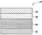
본 발명의 또 다른 실시태양에 따르면, 유기 발광 디바이스는 하나 이상의 잠재적 전하-공여체 물질의 광활성화 또는 열적 활성화 생성물을 포함하는 하나 이상의 활성화된 층을 포함한다. 도 2를 참조하여 보면, 발광 디바이스(20)의 제 2의 예시적인 실시태양이 도시되어 있다. 도시된 실시태양에서, 발광 디바이스(20)는 제 1 전극(22), 하나 이상의 잠재적 활성제 물질의 광활성화 또는 열적 활성화 생성물을 갖는 활성화된 층(24), 전기활성층(26) 및 제 2 전극(28)을 포함하는 것으로 도시되어 있다. 몇 가지 실시태양에서, 활성화된 유기 전기활성층은 발광성 중합체 층이다. 또 다른 실시태양에서, 활성화된 유기 전기활성층은 전하 수송층이다.According to another embodiment of the present invention, the organic light emitting device comprises one or more activated layers comprising a photoactivation or thermal activation product of one or more potential charge-donor materials. Referring to FIG. 2, a second exemplary embodiment of a
활성화된 층은 정공 수송층 물질, 정공 주입층 물질, 전자 수송층 물질, 전자 주입층 물질, 광 흡수층 물질, 캐소드층 물질, 애노드층 물질 또는 전기발광층 물질, 또는 이들의 임의의 조합을 더 포함할 수 있다. 활성화된 층은 하나 이상의 파장에서의 광-활성화 생성물을 포함할 수 있다. OLED는 중합체 기판과 같은 기판층을 더 포함할 수 있지만, 중합체 기판으로 국한되는 것은 아니다.The activated layer may further comprise a hole transport layer material, a hole injection layer material, an electron transport layer material, an electron injection layer material, a light absorbing layer material, a cathode layer material, an anode layer material or an electroluminescent layer material, or any combination thereof. . The activated layer may comprise photo-activation products at one or more wavelengths. The OLED may further comprise a substrate layer, such as a polymer substrate, but is not limited to a polymer substrate.
몇 가지 실시태양에서, 활성화된 층은 100중량%의 활성제 물질을 포함한다. 특정의 다른 실시태양에서, 활성제 물질은 활성화된 층의 약 99중량% 내지 1중량% 범위로 존재한다. 다른 실시태양에서, 활성제 물질은 활성화된 층 조성의 약 90% 내지 약 20% 범위로 존재한다. 또 다른 실시태양에서, 활성제 물질은 활성화된 층의 약 90% 내지 약 50% 범위로 존재한다. 몇 가지 다른 실시태양에서, 활성제 물질은 총 활성화된 층 조성의 100ppm 정도의 적은 양으로 존재할 수 있다.In some embodiments, the activated layer comprises 100% by weight of active agent material. In certain other embodiments, the active agent material is present in the range of about 99% to 1% by weight of the activated layer. In other embodiments, the activator material is present in the range of about 90% to about 20% of the activated layer composition. In another embodiment, the activator material is present in the range of about 90% to about 50% of the activated layer. In some other embodiments, the activator material may be present in amounts as low as 100 ppm of the total activated layer composition.
본 발명의 몇 가지 실시태양에서, 유기 발광 디바이스는 패턴화된다. 이러한 패턴은 알파벳, 숫자 및 기하학적 구조와 같이 규칙적일 수 있지만, 그들로 국한되는 것은 아니다. 이러한 패턴은 또한 임의적이고 불규칙할 수도 있다. OLED 디바이스는 광 또는 열 유도된 공간 선택적 활성화에 의해 패턴화할 수 있다. 공간 선택적 활성화는 미리 규격화된 마스크(pre-machined mask), 네거티브 필름, 또는 기타 다른 수단을 이용하여 달성한다.In some embodiments of the invention, the organic light emitting device is patterned. Such patterns can be regular, such as, but not limited to alphabets, numbers, and geometries. This pattern may also be arbitrary and irregular. OLED devices can be patterned by light or heat induced spatially selective activation. Spatially selective activation is accomplished using a pre-machined mask, negative film, or other means.
본 발명의 특정의 다른 실시태양에서, 이러한 패턴화는 또한 공간 선택적 패시베이션에 의해 달성될 수도 있다. 선택적 패시베이션은 활성화된 영역과 접촉하는 상대 전하-공여체 물질을 선택적으로 조사하는 탈-활성화를 포함한다.In certain other embodiments of the present invention, such patterning may also be accomplished by spatially selective passivation. Selective passivation includes de-activation to selectively irradiate a relative charge-donor material in contact with the activated region.
도 3을 참조하면, 또 다른 예시적인 실시태양의 발광 디바이스(30)를 도시한 것이다. 도시된 실시태양에서, 발광 디바이스(30)는 제 1 전극(32), 하나 이상의 잠재적 전하-공여체 물질의 광 또는 열적 활성화 생성물을 포함하는 활성화된 영역(34)을 갖는 선택적으로 활성화된 전기활성 층(33), 및 하나 이상의 잠재적 활성제 물질을 갖는 비-활성화된 영역(36)을 포함하는 것으로 도시되어 있다. 이러한 디바이스는 추가의 유기 전기활성층(38) 및 제 2 전극(40)을 더 포함한다. 선택적으로 활성화된 층(33)에서, 층의 단지 특정의 부분 또는 구획만이 선택적으로 활성화되는 반면, 특정 구획이 잠재적 활성제 물질을 가진 채로 잔류하거나 또는 일정 영역이 탈활성화되거나 또는 부동화될 수 있다. 이러한 선택적 활성화에 의해 OLED를 패턴화할 수 있다. 이러한 패턴화는 그로 국한되는 것은 아니지만 알파벳 또는 숫자 또는 기하학적 패턴과 같은 규칙적인 형상을 포함할 수 있으며, 또한 임의적인 형상 및 패턴을 포함할 수도 있다.3, a
도 4에 도시된 실시태양에서, 발광 디바이스(42)는 제 1 전극(44), 하나 이상의 잠재적 활성제 물질의 광 또는 열적 활성화 생성물을 갖는 제 1 활성화된 층(46), 하나 이상의 잠재적 활성제 물질의 광 또는 열적 활성화 생성물을 갖는 제 2 활성화된 층(48) 및 제 2 전극(50)을 포함한다. 비제한적 실례에서, 층(46)은 정공을 주입 및/또는 수송할 수 있는 방식으로 활성화되며, 층(48)은 전자를 주입 및/또는 수송할 수 있는 방식으로 활성화된다.In the embodiment shown in FIG. 4, the
도 5를 참조하면, 또 다른 예시적인 실시태양의 발광 디바이스(52)를 도시한 것이다. 도시된 실시태양에서, 발광 디바이스(52)는 제 1 전극(54), 하나 이상의 잠재적 전하-공여체 물질의 광 또는 열적 활성화 생성물을 갖는 제 1 활성화된 층(56) 및 하나 이상의 잠재적 전하-공여체 물질의 광 또는 열적 활성화 생성물을 갖는 제 2 활성화된 층(60)을 포함하는 것으로 도시되어 있다. 이러한 디바이스는 2개의 활성화된 층사이에 전기활성 층(58), 및 제 2 전극(62)을 더 포함할 수 있다. 비제한적 실례에서, 제 1 전극(54)은 애노드이며, 제 2 전극(62)은 캐소드이 다.Referring to FIG. 5, there is shown a
도 6에 도시된 실시태양에서, 탠덤형 발광 디바이스(tandem light emitting device)(64)는 인듐 주석 산화물(ITO)과 같은 애노드(66), 하나 이상의 잠재적 전하-공여체 물질의 광 또는 열적 활성화 생성물을 갖는 정공 주입층과 같은 활성화된 전기활성 층(68), 발광성 중합체 층(70), 투명 캐소드(72), 하나 이상의 잠재적 전하-공여체 물질의 광 또는 열적 활성화 생성물을 갖는 제 2 활성화된 정공 주입층(74), 제 1 발광층과 동일한 다른 파장에서 발광하는 제 2 전기활성 층(76) 및 캐소드(78)를 포함한다.In the embodiment shown in FIG. 6, tandem
전하 수송층 물질의 비제한적 실례로는 저분자량 내지 중간 분자량(예를 들면 약 200,000 미만)의 유기 분자, 폴리(3,4-에틸렌다이옥시싸이오펜)(PEDOT), 폴리아닐린, 폴리(3,4-프로필렌다이옥시싸이오펜)(PProDOT), 폴리스타이렌설포네이트(PSS), 폴리바이닐 카바졸(PVK) 또는 유사 물질, 또는 이들의 조합이 포함된다.Non-limiting examples of charge transport layer materials include organic molecules of low to medium molecular weight (eg less than about 200,000), poly (3,4-ethylenedioxythiophene) (PEDOT), polyaniline, poly (3,4- Propylenedioxythiophene) (PProDOT), polystyrenesulfonate (PSS), polyvinyl carbazole (PVK) or similar materials, or combinations thereof.
정공 수송층 물질의 비제한적 실례로는 트라이아릴다이아민, 테트라페닐다이아민, 방향족 3차 아민, 하이드라존 유도체, 카바졸 유도체, 트라이아졸 유도체, 이미다졸 유도체, 아미노기를 갖는 옥사다이아졸 유도체, 폴리싸이오펜 및 유사 물질이 포함된다. 정공 차단층용으로 적합한 물질은 폴리(N-바이닐 카바졸) 및 유사 물질을 포함한다.Non-limiting examples of hole transport layer materials include triaryldiamine, tetraphenyldiamine, aromatic tertiary amines, hydrazone derivatives, carbazole derivatives, triazole derivatives, imidazole derivatives, oxadiazole derivatives having amino groups, poly Thiophene and similar materials. Suitable materials for the hole blocking layer include poly (N-vinyl carbazole) and similar materials.
정공 주입 증강층 물질의 비제한적 실례로는 3,4,9,10-페릴렌테트라-카복실산 이무수물, 비스(1,2,5-싸이아다이아졸로)-p-퀴노비스(1,3-다이싸이올) 및 유사 물질과 같은 아릴렌계 화합물이 포함된다.Non-limiting examples of hole injection enhancement layer materials include 3,4,9,10-perylenetetra-carboxylic dianhydride, bis (1,2,5-thiadiazol) -p-quinobis (1,3- Arylene-based compounds such as dithiol) and the like.
전자 주입 증강층 물질 및 전자 수송층 물질용으로 적합한 물질은 옥사다이아졸 유도체, 페릴렌 유도체, 피리딘 유도체, 피리미딘 유도체, 퀴놀린 유도체, 퀴녹살린 유도체, 다이페닐퀴논 유도체, 나이트로-치환된 플루오렌 유도체 및 유사 물질과 같은 금속 유기 착체를 포함한다.Suitable materials for the electron injection enhancement layer material and the electron transport layer material are oxadiazole derivatives, perylene derivatives, pyridine derivatives, pyrimidine derivatives, quinoline derivatives, quinoxaline derivatives, diphenylquinone derivatives, nitro-substituted fluorene derivatives And metal organic complexes such as analogous materials.
발광층에 사용될 수 있는 물질의 비제한적 실례에는 폴리(N-바이닐카바졸)(PVK) 및 그의 유도체; 폴리(알킬플루오렌), 예를 들면 폴리(9,9-다이헥실플루오렌), 폴리(다이옥틸플루오렌) 또는 폴리{9,9-비스(3,6-다이옥사헵틸)-플루오렌-2,7-다이일}과 같은 폴리플루오렌 및 그의 유도체; 폴리(2-데실옥시-1,4-페닐렌) 또는 폴리(2,5-다이헵틸-1,4-페닐렌)과 같은 폴리(p-페닐렌)(PPP) 및 그의 유도체; 다이알콕시-치환된 PPV 및 시아노-치환된 PPV와 같은 폴리(p-페닐렌 바이닐렌)(PPV) 및 그의 유도체; 폴리(3-알킬싸이오펜), 폴리(4,4'-다이알킬-2,2'-바이싸이오펜), 폴리(2,5-싸이에닐렌 바이닐렌)과 같은 폴리싸이오펜 및 그의 유도체; 폴리(피리딘 바이닐렌) 및 그의 유도체; 폴리퀴녹살린 및 그의 유도체; 및 폴리퀴놀린 및 그의 유도체가 포함된다. 하나의 특정 실시태양에서, 적합한 발광 물질은 N,N-비스(4-메틸페닐)-4-아닐린으로 말단 캡핑된 폴리(9,9-다이옥틸플루오레닐-2,7-다이일)이다. 하나 이상의 이러한 중합체 및 다른 중합체를 기본으로 하는 중합체 또는 공중합체의 혼합물도 또한 사용될 수 있다.Non-limiting examples of materials that can be used in the light emitting layer include poly (N-vinylcarbazole) (PVK) and derivatives thereof; Poly (alkylfluorene), for example poly (9,9-dihexylfluorene), poly (dioctylfluorene) or poly {9,9-bis (3,6-dioxaheptyl) -fluorene- Polyfluorene and derivatives thereof such as 2,7-diyl}; Poly (p-phenylene) (PPP) and derivatives thereof such as poly (2-decyloxy-1,4-phenylene) or poly (2,5-diheptyl-1,4-phenylene); Poly (p-phenylene vinylene) (PPV) and derivatives thereof such as dialkoxy-substituted PPV and cyano-substituted PPV; Polythiophenes and derivatives thereof such as poly (3-alkylthiophene), poly (4,4'-dialkyl-2,2'-bithiophene), poly (2,5-thioenylene vinylene); Poly (pyridine vinylene) and derivatives thereof; Polyquinoxaline and its derivatives; And polyquinoline and its derivatives. In one particular embodiment, a suitable luminescent material is poly (9,9-dioctylfluorenyl-2,7-diyl) end capped with N, N-bis (4-methylphenyl) -4-aniline. Mixtures of one or more such polymers and polymers or copolymers based on other polymers may also be used.
발광층에 사용되는 다른 부류의 적합한 물질은 폴리실란이다. 전형적으로, 폴리실란은 다양한 알킬 및/또는 아릴 측쇄로 치환된 선형 규소-주쇄 중합체이다. 이는 중합체 주쇄를 따라 비편재된 시그마-결합 전자를 갖는 준 일차원 물질(quasi one-dimensional material)이다. 폴리실란의 예로는 폴리(다이-n-부틸실란), 폴리(다이-n-펜틸실란), 폴리(다이-n-헥실실란), 폴리(메틸페닐실란) 및 폴리{비스(p-부틸페닐)실란}을 포함한다.Another class of suitable materials used in the light emitting layer is polysilane. Typically, polysilanes are linear silicon-backbone polymers substituted with various alkyl and / or aryl side chains. It is a quasi one-dimensional material with sigma-bonded electrons unlocalized along the polymer backbone. Examples of polysilanes include poly (di-n-butylsilane), poly (di-n-pentylsilane), poly (di-n-hexylsilane), poly (methylphenylsilane) and poly {bis (p-butylphenyl) Silane}.
전기활성 디바이스에 적합한 캐소드 물질은 전형적으로는 낮은 일함수 값을 갖는 물질을 포함한다. 캐소드 물질의 비제한적 실례는 K, Li, Na, Mg, Ca, Sr, Ba, Al, Ag, Au, In, Sn, Zn, Zr, Sc, Y, Mn, Pb, 란타나이드 계열의 원소, 이들의 합금, 특히 Ag-Mg 합금, Al-Li 합금, In-Mg 합금, Al-Ca 합금 및 Li-Al 합금, 및 이들의 혼합물과 같은 물질을 포함한다. 캐소드 물질의 다른 예는 알칼리금속 플루오라이드, 또는 알칼리토금속 플루오라이드, 또는 이러한 플루오라이드의 혼합물을 포함할 수 있다. 인듐 주석 산화물, 산화주석, 산화인듐, 산화아연, 인듐 아연 산화물, 아연 인듐 주석 산화물, 산화안티몬, 탄소 나노튜브, 및 이들의 혼합물과 같은 다른 캐소드 물질도 또한 적합하다. 다르게는, 캐소드를 2개의 층으로 만들어 전자 주입을 향상시킬 수 있다. 비제한적 실례는 LiF 또는 NaF로 이루어진 내층에 이어 알루미늄 또는 은으로 이루어진 외층을, 또는 칼슘으로 이루어진 내층에 이어 알루미늄 또는 은으로 이루어진 외층을 포함하지만, 그로 국한되는 것은 아니다.Suitable cathode materials for electroactive devices typically include materials with low work function values. Non-limiting examples of cathode materials include K, Li, Na, Mg, Ca, Sr, Ba, Al, Ag, Au, In, Sn, Zn, Zr, Sc, Y, Mn, Pb, lanthanide-based elements, these Alloys, in particular Ag-Mg alloys, Al-Li alloys, In-Mg alloys, Al-Ca alloys and Li-Al alloys, and mixtures thereof. Other examples of cathode materials may include alkali metal fluorides, or alkaline earth metal fluorides, or mixtures of such fluorides. Other cathode materials such as indium tin oxide, tin oxide, indium oxide, zinc oxide, indium zinc oxide, zinc indium tin oxide, antimony oxide, carbon nanotubes, and mixtures thereof are also suitable. Alternatively, the cathode can be made of two layers to improve electron injection. Non-limiting examples include, but are not limited to, an inner layer of LiF or NaF, followed by an outer layer of aluminum or silver, or an inner layer of calcium, followed by an outer layer of aluminum or silver.
전기활성 디바이스용으로 적합한 애노드 물질은 전형적으로는 높은 일함수 값을 갖는 물질을 포함한다. 애노드 물질의 비제한적 실례는 인듐 주석 산화물(ITO), 산화주석, 산화인듐, 산화아연, 인듐 아연 산화물, 니켈, 금 및 유사 물질, 및 이들의 혼합물을 포함한다.Suitable anode materials for electroactive devices typically include materials with high work function values. Non-limiting examples of anode materials include indium tin oxide (ITO), tin oxide, indium oxide, zinc oxide, indium zinc oxide, nickel, gold and similar materials, and mixtures thereof.
기판의 비제한적 실례에는 열가소성 중합체, 폴리(에틸렌 테레프탈레이트), 폴리(에틸렌 나프탈레이트), 폴리에테르설폰, 폴리카보네이트, 폴리이미드, 아크릴레이트, 폴리올레핀, 유리, 금속 및 유사 물질, 및 이들의 조합이 포함된다.Non-limiting examples of substrates include thermoplastic polymers, poly (ethylene terephthalate), poly (ethylene naphthalate), polyethersulfones, polycarbonates, polyimides, acrylates, polyolefins, glass, metals and similar materials, and combinations thereof Included.
본 발명의 유기 발광 디바이스는 하나 이상의 내마모성층, 접착층, 내화학성층, 발광층, 방사선 흡수층, 방사선 반사층, 차단층, 평면화층, 광학적 확산층 및 이들의 조합과 같은 추가의 층을 포함할 수 있지만, 그들로 국한되는 것은 아니다.The organic light emitting device of the present invention may comprise additional layers such as one or more wear resistant layers, adhesive layers, chemical resistant layers, light emitting layers, radiation absorbing layers, radiation reflecting layers, blocking layers, planarizing layers, optical diffusing layers and combinations thereof, but It is not limited to.
또 다른 실시태양에서, 도 7 내지 도 24를 참조로 하여 하기에서 더 설명되는 바와 같이, 본 발명은 유기 발광 디바이스를 제조하는 방법에 관한 것이다. 이러한 방법은 일반적으로는 기판을 제공하는 단계 및 상기 기판상에 하나 이상의 잠재적 활성제 물질을 포함하는 하나 이상의 유기 디바이스 층을 배치하는 단계를 포함한다. 기판은 전형적으로는 전극이다. 전극 기판은 또한 중합체 기판과 같은 다른 기판을 포함할 수도 있지만 그들로 국한되는 것은 아니다.In another embodiment, as described further below with reference to FIGS. 7-24, the present invention relates to a method of manufacturing an organic light emitting device. Such methods generally include providing a substrate and disposing one or more organic device layers comprising one or more potential activator materials on the substrate. The substrate is typically an electrode. The electrode substrate may also include other substrates such as, but not limited to, polymer substrates.
본 발명의 방법은 잠재적 활성제 물질을 광-활성화 또는 열-활성화시켜 염기나 산을 발생시키는 단계를 더 포함한다. 이러한 활성화는 유기 발광 디바이스를 제조하는 도중에 특정 단계에서 실시될 수 있다. 이러한 활성화는 또한 디바이스를 조립한 후 디바이스의 수명 기간중에 어느 때라도 실시될 수 있다. 본 발명의 방법은 패턴화 단계 또는 공간 선택적 활성화 단계를 더 포함할 수 있다. 패턴화는 알파벳, 숫자 및 기하학적 구조와 같이 규칙적일 수 있지만, 그로 국한되는 것은 아니다. 패턴화는 또한 임의적이고 불규칙할 수도 있다. 공간 선택적 활성화는 미리 기계가공된 마스크, 네거티브 필름 또는 기타 다른 수단을 사용하여 달성 한다. 이러한 활성화는 하나 이상의 파장에서의 하나 이상의 잠재적 전하-공여체 물질의 광활성화를 포함할 수 있다.The method further includes the step of photo-activating or heat-activating the latent activator material to generate bases or acids. This activation can be done at a particular step during the manufacture of the organic light emitting device. This activation can also be done at any time during the lifetime of the device after assembling the device. The method may further comprise a patterning step or a spatial selective activation step. Patterning can be regular, such as, but not limited to alphabets, numbers, and geometries. Patterning may also be arbitrary and irregular. Spatial selective activation is achieved using a pre-machined mask, negative film or other means. Such activation may include photoactivation of one or more potential charge-donor materials at one or more wavelengths.
몇 가지 실시태양에서, 본 발명의 방법은 공간 선택적 패시베이션 단계를 더 포함할 수 있는데, 이때 공간 선택적 패시베이션은 활성화된 영역과 접촉하는 잠재적 상대 활성제 물질을 조사하는 단계를 포함한다. 예를 들면, p-활성화된 층은 p-활성화된 층과 접촉하는 광염기-발생제를 조사함으로써 선택적으로 부동화시키거나 탈활성화시킬 수 있다. OLED의 패턴화도 또한 공간 선택적 패시베이션에 의해 달성될 수 있다.In some embodiments, the methods of the present invention may further comprise a space selective passivation step, wherein the space selective passivation comprises irradiating a potential counter activator material in contact with the activated region. For example, the p-activated layer can be selectively passivated or deactivated by irradiating a photobase-generating agent in contact with the p-activated layer. Patterning of OLEDs can also be achieved by space selective passivation.
본 발명의 방법은 기판상에 정공 수송층 물질, 정공 주입층 물질, 전자 수송층 물질, 전자 주입층 물질, 광흡수층 물질, 캐소드층 물질, 애노드층 물질 또는 전기발광층 물질, 또는 이들의 임의의 조합을 배치하는 단계를 더 포함할 수 있다. 몇 가지 실시태양에서, 이러한 방법은 각 층들을 잠재적 활성제 물질 또는 잠재적 활성제 물질의 활성화 생성물을 포함하는 하나 이상의 층과 함께 적층하는 단계를 더 포함할 수 있다.The method of the present invention places a hole transport layer material, a hole injection layer material, an electron transport layer material, an electron injection layer material, a light absorption layer material, a cathode layer material, an anode layer material or an electroluminescent layer material, or any combination thereof on a substrate. It may further comprise the step. In some embodiments, the method may further comprise laminating each layer with one or more layers comprising a latent activator material or an activation product of the latent activator material.
몇 가지 실시태양에서, 잠재적 활성제 물질은 다른 OLED층 물질과 함께 증착된다. 예를 들면, 잠재적 활성제 물질은 발광층 물질과 함께 증착될 수 있다. 다른 실시태양에서, 잠재적 활성제 물질은 OLED층의 상부에 증착된다. 활성화시에, 표면에서 방출된 활성제 물질이 하부층을 개질시킨다.In some embodiments, the latent activator material is deposited along with other OLED layer materials. For example, the latent activator material may be deposited with the light emitting layer material. In another embodiment, the latent activator material is deposited on top of the OLED layer. Upon activation, the activator material released from the surface modifies the underlying layer.
층을 증착 또는 배치하는 방법은 방사 코팅, 딥 코팅, 리버스롤(reverse roll) 코팅, 와이어-권취(wire-wound) 또는 메이어 로드(Mayer rod) 코팅, 다이렉 트 및 오프셋 그라비어 코팅(direct and offset gravure coating), 슬롯 다이 코팅, 블레이드 코팅, 핫멜트 코팅, 커튼 코팅, 나이프 오버롤 코팅(knife over roll coating), 압출, 에어 나이프 코팅(air knife coating), 분무, 회전식 스크린 코팅, 다층 슬라이드 코팅, 공압출, 메니스커스 코팅(meniscus coating), 콤마식 및 마이크로 그라비어 코팅, 리쏘그래피 공정, 랭뮤어 공정(langmuir process) 및 플래시 증발, 증착, 플라스마-증강식 화학증착("PECVD")(plasma-enhanced chemical-vapor deposition), 무선 주파수 플라즈마-증강식 화학증착("RFPECVD")(radio-frequency plasma-enhanced chemical-vapor deposition), 팽창식 열-플라즈마 화학증착("ETPCVD")(expanding thermal-plasma chemical-vapor deposition), 이로 국한되는 것은 아니지만 반응성 스퍼터링을 포함한 스퍼터링, 전자-사이클로트론-공명 플라즈마-증강식 화학증착("ECRPECVD")(electron-cyclotron-resonance plasma-enhanced chemical-vapor deposition), 유도 결합식 플라즈마-증강식 화학증착("ICPECVD")(inductively coupled plasma-enhanced chemical-vapor deposition) 및 유사 기법, 및 이들의 조합과 같은 기법을 포함하지만, 그들로 국한되는 것은 아니다.The method of depositing or placing a layer may include radiation coating, dip coating, reverse roll coating, wire-wound or Mayer rod coating, direct and offset gravure coating. gravure coating, slot die coating, blade coating, hot melt coating, curtain coating, knife over roll coating, extrusion, air knife coating, spraying, rotary screen coating, multilayer slide coating, coextrusion , Meniscus coating, comma and micro gravure coating, lithography process, langmuir process and flash evaporation, deposition, plasma-enhanced chemical deposition ("PECVD") -vapor deposition, radio-frequency plasma-enhanced chemical vapor deposition ("RFPECVD"), expanding thermal-plasma chemical vapor deposition ("ETPCVD") vapor deposition, sputtering including but not limited to reactive sputtering, electron-cyclotron-resonance plasma-enhanced chemical-vapor deposition ("ECRPECVD"), inductively coupled plasma- Techniques such as, but not limited to, inductively coupled plasma-enhanced chemical-vapor deposition ("ICPECVD") and similar techniques, and combinations thereof.
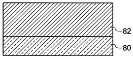
도 7 내지 도 22는 본 발명의 양태에 따른, 도 1 내지 도 6에 도시된 유기 발광 디바이스를 제조하는 예시적인 공정의 단면도이다. 도 7에 도시된 전극(80)은 후속 층들을 증착시키기 위한 기판으로서 사용된다. 전극의 예는 ITO 애노드이다. 특정 실시태양에서, 전극은 중합체 기판을 더 포함할 수 있다. 전극을 UV/오존 표면 처리한 다음 후속 층들을 증착시킬 수 있다. 본원에서 사용된 디바이스 하부구조물(device sub-structures)은 하나 이상의 기판층, 하나 이상의 전극층, 하나 이상의 잠재적 활성화된 층, 하나 이상의 활성화된 층, 하나 이상의 전기활성층, 또는 그들로 국한되는 것은 아니지만 접착층과 같은 하나 이상의 추가의 층, 및 차단층을 포함할 수 있다. 몇 가지 실시태양에서는, 2개 이상의 디바이스 하부구조물을 서로상에 증착시키거나 배치하여 유기 발광 디바이스를 형성시킬 수 있다. 다른 실시태양에서는, 그로 국한되는 것은 아니지만 적층과 같은 공정을 이용하여 2개 이상의 디바이스 하부구조물을 결합시켜 유기 발광 디바이스를 형성시킬 수 있다.7-22 are cross-sectional views of an exemplary process for manufacturing the organic light emitting device shown in FIGS. 1-6, in accordance with aspects of the present invention. The
도 8에 도시된 바와 같이, 잠재적 활성제 물질을 갖는 잠재적 활성화된 전기활성층(82)은 전극상에 증착된다. 잠재적 활성화된 전기활성층(82)은 유기 전기활성층일 수 있으며, 예를 들면, 정공 수송물질 또는 발광물질을 더 포함할 수 있다. 도 9에 도시된 바와 같이, 이어서 참조 번호(84)로 표시된 바와 같이, 각각 열 또는 광선을 적용하고 열적 활성화 또는 광활성화시켜 잠재적 활성제 물질을 포함한 잠재적 활성화된 전기활성층(82)을 활성화시킨다. 잠재적 활성화된 전기활성층(82)의 활성화가 도 10에 도시된 바와 같은 활성화된 전기활성층(86)내에서 일어나 디바이스 하부구조물(89)을 형성한다. 다른 층들이 하부구조물상에 증착되어 발광 디바이스를 형성할 수 있다. 이러한 공정은 적어도 하나 이상의 전기활성층(88)을 증착시켜 더 진행시킬 수 있다. 마지막으로, 도 11에 도시된 바와 같이, 캐소드층과 같은 제 2 전극(90)을 전기활성층(88)상에 증착하여 발광 디바이스(20)를 형성시킬 수 있다(도 2 참조).As shown in FIG. 8, a latent activated
다른 방법으로, 이러한 공정은 도 8에 도시된 공정 단계에서 도 12에 도시된 공정 단계까지 진행시킬 수 있으며, 이때 전기활성층(88)이 잠재적 활성화된 전기활성층(82)상에 증착된다. 전극(90)을 전기활성층(82)상에 증착할 때 디바이스(10)(도 1 참조)가 완성된다. 열 또는 광활성화(84)를 적용함으로써 잠재적 활성화된 전기활성층(82)을 계속적으로 활성화시켜, 도 15에 도시된 바와 같은 활성화된 층(86) 및 디바이스(20)를 형성시킬 수 있다.Alternatively, this process can proceed from the process step shown in FIG. 8 to the process step shown in FIG. 12, wherein an
또 다른 공정 경로에서, 이러한 공정은 도 8에 도시된 공정 단계에서 도 16에 도시된 공정 단계까지 진행시킬 수 있으며, 이때에는 전기활성층(88)이 선택적으로 활성화될 수 있다. 선택적 활성화는 OLED 디바이스의 패턴화를 일으킬 수 있다. 이러한 패턴화는 바람직하게는 규칙적이거나 임의적일 수 있다. 도 17에 도시된 바와 같이, 선택적 활성화는 활성제 물질을 갖는 활성화된 영역(92) 및 아직도 잠재적 활성화된 영역(94)을 갖는 패턴화된 층(91)을 생성시킨다. 전기활성층(88) 및 전극층(90)과 같은 추가의 층들을 증착하여 도 18에 도시된 바와 같은 발광 디바이스(30)를 제조할 수 있다.In another process path, this process may proceed from the process step shown in FIG. 8 to the process step shown in FIG. 16, in which the
다른 방법으로, 이러한 공정은 도 12에 도시된 공정 단계에서 도 19에 도시된 공정 단계까지 진행시킬 수 있으며, 이때에는 제 2 잠재적 활성화된 층(95)이 전기활성층(88)상에 증착될 수 있다. 잠재적 활성화된 층(95)을 광 또는 열적 활성화(94)시켜 도 20에 도시된 바와 같은 제 2 활성화된 층(96)을 제공한다. 도 21에 도시된 바와 같이, 제 2 전극을 제 2 활성화된 층(96)상에 배치하여 디바이스(52)를 생성시킬 수 있다. 비제한적 실례에서는, 제 1 활성화된 층(86)은 p-활 성화된 층이며, 제 2 활성화된 층(96)은 n-활성화된 층이다.Alternatively, this process can proceed from the process step shown in FIG. 12 to the process step shown in FIG. 19, wherein a second potentially activated
다른 방법으로, 전극(80), 제 1 활성화된 층(86) 및 추가의 전기활성층(88)을 포함한 제 1 디바이스 하부구조물(89)이 형성되는, 도 10에 도시된 공정 단계를 포함하는 공정이 또한 도 22에 도시된 공정 단계를 포함할 수도 있으며, 이때에는 활성화된 층(96) 및 제 2 전극 기판층(90)을 포함하는 제 2 하부구조물(97)이 형성된다. 활성화된 층(96)은 도 19에 도시된, 층(95)과 같은 잠재적 활성화된 층(95)을 활성화시킴으로써 형성될 수 있다. 제 1 및 제 2 디바이스 하부구조물(89 및 97)을 제조하는 공정 단계에 이어서, 2개의 하부구조물을 함께 적층하여 도 21에 도시된 바와 같은 디바이스(52)를 형성할 수 있다. 몇 가지 실시태양에서, 이러한 적층은 제 1 디바이스 하부구조물 및 제 2 디바이스 하부구조물을 함께 합친 다음, 구조물에 압력 또는 열 또는 이들의 조합을 적용함으로써 실시한다. 하나의 실시태양에서, 제 1 디바이스 하부구조물(89) 및 제 2 디바이스 하부구조물(97)을 오버레이시킨 다음 롤 적층기에 통과시켜 디바이스(52)를 형성한다. 몇 가지 실시태양에서, 이러한 적층은 150℃의 온도에서 실시한다. 특정 실시태양에서는, 도 10 및 도 19에 도시된 바와 같이 하부구조물내의 잠재적 활성제 물질을 활성화한 다음 적층시킬 수 있다. 다른 실시태양에서는, 적층후에 하부구조물내의 잠재적 활성제 물질을 활성화함으로써, 적층시에 제 1 및/또는 제 2 디바이스 구조물이 잠재적 활성화된 층을 포함할 수 있다. 비제한적 실례에서, 제 1 및 제 2 디바이스 구조물은 하나 이상의 기판층, 하나 이상의 전극, 하나 이상의 잠재적 활성화된 층, 하나 이상의 활성화된 층, 하나 이상의 전기활성층, 또는 그로 국한되는 것은 아니지만 접착층과 같은 하나 이상의 다른 층 및 차단층을 포함할 수 있다.Alternatively, a process comprising the process step shown in FIG. 10, in which a
도 23은 본 발명 기술의 양태에 따라 유기 발광 디바이스를 제조하는 예시적인 공정(100)을 도시한 생산 공정도이다. 이러한 공정(100)은 전극일 수 있는 기판(102)을 제공하는 단계(도 7 참조), 예를 들면, 잠재적 활성제 물질을 포함하는 층을 기판(104)상에 배치하는 단계(도 8 참조), 하나 이상의 추가적인 유기 층을 기판(106)상에 배치하는 단계(도 12 참조), 및 이어서 제 2 전극을 기판(108)상에 배치하는 단계(도 13 참조)를 포함한다.23 is a production flow diagram illustrating an
도 24는 본 발명 기술의 양태에 따라 유기 발광 디바이스를 제조하는 예시적인 공정(110)을 도시한 생산 공정도이다. 이러한 공정(110)은, 예를 들면, 전극일 수 있는 기판을 제공하는 단계(112)에서 시작된다(도 7 참조). 이러한 공정(110)은 잠재적 활성제 물질을 포함하는 층을 기판상에 배치하는 단계(114)로 진행한다(도 8 참조). 단계(116)에서는, 광활성화 또는 열적 활성화에 의해 이러한 공정을 진행시켜 활성제 물질을 활성화시킨다(도 9 참조).24 is a production flow diagram illustrating an
도 25는 본 발명 기술의 양태에 따라 유기 발광 디바이스를 제조하는 예시적인 공정(118)을 도시한 생산 공정도이다. 이러한 공정(118)의 단계(120)에서는, 예를 들면, 전극일 수 있는 기판이 제공된다(도 7 참조). 이러한 공정(118)은 잠재적 활성제 물질을 포함하는 층을 기판상에 배치하는 단계(122)로 진행한다(도 8 참조). 단계(124)에서는, 광활성화 또는 열적 활성화에 의해 이러한 공정을 진행시켜 활성제 물질을 활성화시키고(도 9 참조), 이어서 하나 이상의 추가의 유기층을 기판(126)상에 배치하는 단계로 진행시킨 다음(도 10 참조), 마지막으로 기판상 에 제 2 전극을 배치하는 단계(128)로 진행한다(도 11 참조).25 is a production flow diagram illustrating an
추가적인 설명이 없이도, 당업자는 본원에 기술된 내용을 이용하여 본 발명을 완전하게 이용할 수 있을 것이라 생각된다. 하기 실시예는 청구된 본 발명을 실시하는데 있어서 당업자에게 추가적인 지침을 제공하기 위하여 포함된 것이다. 제공된 실시예는 단지 본 발명의 교시내용에 도움을 주는 대표적인 작업일 뿐이다. 따라서, 이들 실시예는 어떠한 방법으로든 첨부된 특허청구의 범위에 정의된 바와 같은 본 발명을 국한하려는 것이 아니다.Without further elaboration, it is believed that one skilled in the art can, using the teachings herein, utilize the present invention to its fullest extent. The following examples are included to provide additional guidance to those skilled in the art in practicing the claimed invention. The examples provided are merely representative of the work aiding the teachings of the present invention. Accordingly, these examples are not intended to limit the invention as defined in the appended claims in any way.
켈빈 프로브(Kelvin probe)(KP)는 통상적인 프로브에 대한 전압(V) 단위의 접촉 전위차(contact potential difference)(CPD, 유효 표면 일함수(effective surface work function)에 있어서의 변화에 상응함)를 측정함으로써 전도성/반전도성 물질의 유효 표면 일함수에 있어서의 변화를 측정하는데 사용되는 진동 커패시터 기법(vibrating capacitor technique)이다. KP 측정은 디지털 켈빈 프로브 KP6500을 사용하여 실시하였다.The Kelvin probe (KP) is used to measure the contact potential difference (CPD, corresponding to a change in the effective surface work function) in voltage (V) for a conventional probe. By vibrating is a vibrating capacitor technique used to measure changes in the effective surface work function of conductive / semiconductive materials. KP measurements were performed using a digital Kelvin probe KP6500.
실시예 1Example 1
본 실시예에서는 알드리히(Aldrich)사로부터 프로필렌 카보네이트중의 0.5중량% 분산액으로서 입수한, 폴리(3,4-에틸렌다이옥시싸이오펜)테트라메타크릴레이트 말단-캡핑된 싸이오펜계 전도성 중합체(PEDOT-TMA)가 사용되었다. 잠재적 활성제 물질로서는 알드리히사로부터 입수한 요오도늄염인 다이페닐요오도늄 헥사플루오로 포스페이트 Ph2IPF6가 사용되었다. 프로필렌 카보네이트중의 2g의 PEDOT-TMA를 1.5ml의 프로필렌 카보네이트중의 100mg의 Ph2IPF6와 혼합하여 PEDOT-TMA 및 Ph2IPF6의 (PEDOT-TMA:Ph2IPF6로서 지칭되는) 혼합물 용액을 제조하였다.In this example, a poly (3,4-ethylenedioxythiophene) tetramethacrylate end-capped thiophene-based conductive polymer obtained from Aldrich as a 0.5 wt% dispersion in propylene carbonate ( PEDOT-TMA) was used. As a potential activator material, diphenyliodonium hexafluoro phosphate Ph 2 IPF 6 , an iodonium salt obtained from Aldrich, was used. A mixture solution of PEDOT-TMA and Ph 2 IPF 6 (referred to as PEDOT-TMA: Ph 2 IPF 6 ) by mixing 2 g of PEDOT-TMA in propylene carbonate with 100 mg of Ph 2 IPF 6 in 1.5 ml of propylene carbonate. Was prepared.
KP 측정을 위한 3개의 샘플(표 1 참조)은 다음과 같이 제조하였다. 어플라이드 필름스 코포레이션(Applied Films Corporation)사로부터 입수한 인듐 주석 산화물(ITO, 약 140nm) 코팅된 유리를 전도성 기판으로서 사용하였다. 샘플 1은 미가공된 예비-세정된 ITO였고, 샘플 2는 ITO, 및 4000rpm의 방사-속도에서 프로필렌 카보네이트중의 용액으로부터 방사-코팅하여 도포한 PEDOT-TMA의 층(약 40nm)으로 구성되었으며, 샘플 3은 ITO, 및 4000rpm의 방사-속도에서 혼합물 용액으로부터 방사-코팅하여 도포한 PEDOT-TMA:Ph2IPF6의 층(약 35nm)으로 구성되었다. 이어서, UV 오존 처리전 및 처리후에 각 샘플에 대해 KP 측정을 실시하였다. UV-오존 처리 및 KP 처리(미국 CA 92618 어빈에 소재한 제라이트 캄파니(Jelight Company)사로부터 입수한 자외선 오존 클리너 모델 42를 사용)는 모두 약 24℃의 실온 및 약 64%의 상대습도를 갖는 주변 환경에서 실시하였다.Three samples (see Table 1) for KP measurements were prepared as follows. Indium tin oxide (ITO, about 140 nm) coated glass obtained from Applied Films Corporation was used as the conductive substrate.
상기 표 1에 열거된 결과로부터 알 수 있는 바와 같이, PEDOT-TMA를 UV-오존처리(활성화된 샘플 2)하던지 하지 않던지(샘플 2)에 무관하게 PEDOT-TMA를 도입하는 것이 ITO 기판의 CPD(및 등가적으로는, 유효 일함수)의 상당한 변화를 유발시키지 않았다. 이와 유사하게, (방사-코팅된) PEDOT-TMA:Ph2IPF6의 존재(샘플 3)는 측정된 CPD를 상당히 변경시키지 않았다. 그러나, PEDOT-TMA:Ph2IPF6 혼합물 층을 UV-오존 처리한 후에는 CPD에 있어서 상당한 감소(등가적으로는, 유효 일함수에 있어서의 증가)가 관찰되었다.As can be seen from the results listed in Table 1 above, the introduction of PEDOT-TMA for PEDOT-TMA with or without UV-ozone treatment (activated sample 2) (sample 2) or CPD of ITO substrate (And, equivalently, effective work function) did not cause a significant change. Similarly, the presence of (radiation-coated) PEDOT-TMA: Ph 2 IPF 6 (Sample 3) did not significantly alter the measured CPD. However, PEDOT-TMA: Ph 2 IPF 6 After UV-ozone treatment of the mixture layer, a significant decrease (equivalently, an increase in the effective work function) in CPD was observed.
실시예 2Example 2
6개의 OLED 디바이스를 제조하였다. 청색-발광 중합체(LEP), ADS329BE[N,N-비스(4-메틸페닐)-아닐린으로 말단-캡핑된 폴리(9,9-다이옥틸플루오레닐-2,7-다이일)]로 이루어진 OLED를 캐나다 소재의 아메리칸 다이 소시즈, 인코포레이티드(American Dye Sources, Inc.)사로부터 입수하여 추가의 정제없이 발광층 물질로서 사용하였다.Six OLED devices were manufactured. OLED consisting of blue-luminescent polymer (LEP), ADS329BE [poly (9,9-dioctylfluorenyl-2,7-diyl) end-capped with N, N-bis (4-methylphenyl) -aniline] Was obtained from American Dye Sources, Inc. of Canada and used as light emitting layer material without further purification.
OLED는 다음과 같이 제조하였다. 표준 포토리쏘그래피 기법을 이용하여 패턴화한 ITO 코팅 유리를 애노드 기판으로서 사용하였다. OLED는 ITO 애노드를 추가의 애노드-활성화 층과 함께 또는 애노드-활성화 층이 없이 사용하지만, 달리는 유사한 구조이다. 하기 표 2에 나타나 있는 바와 같이, 디바이스 B내의 ITO 기판을 ADS329BE를 도포하기 전에 5분 동안 추가로 UV-오존 처리하였다는 것을 제외하고는, 디바이스 A 및 디바이스 B는 모두 동일한 ITO 애노드를 가졌다. 디바이스 D내의 PEDOT-TMA 층을 ADS329BE를 도포하기 전에 약 5분 동안 추가로 UV-오존 처리하였다는 것을 제외하고는, 디바이스 C 및 디바이스 D는 모두 PEDOT-TMA의 동일한 애노드-활성화 층(약 40 내지 45nm)을 가졌다. 디바이스 F내의 PEDOT-TMA:Ph2IPF6 층을 ADS329BE를 도포하기 전에 약 5분 동안 추가로 UV-오존 처리하였다는 것을 제외하고는, 디바이스 E 및 디바이스 F는 모두 PEDOT-TMA:Ph2IPF6의 동일한 애노드-활성화 층(약 35nm)을 가졌다. 이어서, ADS329BE의 층(65±3nm)을 애노드-활성화 층과 함께 또는 애노드-활성화 층없이 그의 p-자일렌중의 용액으로부터 ITO의 상부에 방사-코팅하였다. 애노드-활성화 층 및 ADS329BE 층의 도포 뿐만 아니라 UV-오존 처리 모두 24℃의 실온 및 64%의 상대습도를 갖는 주변 환경에서 실시하였다. 이어서, 샘플을 아르곤으로 충진된 글로브 박스(glovebox)(수분 및 산소는 각각 약 1ppm 미만 및 약 10ppm이었다)로 옮겼다. 다음으로, 이어서 NaF(4nm)/Al(110nm) 이층 캐소드를 ADS329 발광층의 상부에서 열-증발시켰다. 금속화(금속화는 알루미늄과 같은 금속 층을 배치하여 다양한 디바이스 구조물을 전기적으로 연결하거나 상호 연결하는 것을 지칭한다)시킨 후, 디바이스를 미국 뉴저지 08512 크랜베리에 소재한 놀랜드 프로덕츠, 인코포레이티드(Norland products, Inc.)로부터 입수한 광학 접착제 놀랜드 68(Norland 68)를 사용하여 밀봉한 커버 그라스로 캡슐화하였다. 활성 영역은 약 0.2㎠ 였다.OLEDs were prepared as follows. ITO coated glass patterned using standard photolithography techniques was used as the anode substrate. OLEDs use ITO anodes with or without additional anode-activating layers, but are otherwise similar structures. As shown in Table 2 below, both Device A and Device B had the same ITO anode, except that the ITO substrate in Device B was further UV-ozone treated for 5 minutes prior to applying ADS329BE. Device C and Device D are both the same anode-activated layer of PEDOT-TMA (approximately from 40 to 40), except that the PEDOT-TMA layer in device D was further UV-ozone treated for about 5 minutes prior to applying ADS329BE. 45 nm). Both Device E and Device F were PEDOT-TMA: Ph 2 IPF 6 except that the PEDOT-TMA: Ph 2 IPF 6 layer in Device F was further UV-ozone treated for about 5 minutes prior to applying ADS329BE. Had the same anode-activated layer of about 35 nm. A layer of ADS329BE (65 ± 3 nm) was then spin-coated on top of ITO from a solution in p-xylene with or without an anode-activating layer. Both the application of the anode-activated layer and the ADS329BE layer, as well as the UV-ozone treatment, were conducted in an ambient environment with room temperature of 24 ° C. and a relative humidity of 64%. The sample was then transferred to a glovebox filled with argon (moisture and oxygen were less than about 1 ppm and about 10 ppm, respectively). Next, a NaF (4 nm) / Al (110 nm) bilayer cathode was then heat-evaporated on top of the ADS329 light emitting layer. After metallization (metallization refers to the electrical connection or interconnection of various device structures by placing metal layers such as aluminum), the devices are then fabricated by Norland Products, Inc., 08512, Cranberry, NJ. Encapsulated in a sealed cover glass using
디바이스의 측정된 성능 특성이 상기 표 2에 요약되어 있다. UV-오존 처리된 PEDOT-TMA:Ph2IPF6 애노드-활성화 층을 사용한 경우에 처리되지 않은 ITO 애노드를 갖거나 또는 PEDOT-TMA 애노드-활성화 층을 갖는 디바이스에 비하여 상당히 향상된 효율 및 (상응하는 휘도가 1cd/㎡에 도달했을 때의 인가 전압으로서 정의되는) 훨씬 더 낮아진 작동 전압을 갖는 OLED 디바이스가 수득되었음을 알 수 있다. 모든 디바이스가 동일한 타입의 발광층 뿐만 아니라 동일한 타입의 이층 캐소드를 공유하기 때문에, 성능에 있어서의 향상은 ITO 전극이 PEDOT-TMA:Ph2IPF6에 의해 활성화되어 훨씬 더 향상된 정공-주입을 유발한다는 사실에 기인할 수 있다. 측정된 성능 특성은 Ph2IPF6의 존재 및 UV-오존 처리가 관측된 활성화 효과에 기여하는 주요 인자임을 나타낸다.The measured performance characteristics of the device are summarized in Table 2 above. UV-ozone treated Significantly improved efficiency and (corresponding luminance at 1 cd / m 2) compared to devices with unprocessed ITO anode or with PEDOT-TMA anode-activated layer when using PEDOT-TMA: Ph 2 IPF 6 anode-activated layer It can be seen that an OLED device with a much lower operating voltage (defined as the applied voltage when reached) has been obtained. Since all devices share the same type of bilayer cathode as well as the same type of emissive layer, the improvement in performance leads to the fact that the ITO electrode is activated by PEDOT-TMA: Ph 2 IPF 6 , resulting in much improved hole-injection Can be caused by. The measured performance characteristics indicate that the presence of Ph 2 IPF 6 and UV-ozone treatment are the major factors contributing to the observed activation effect.
출원인이 임의의 특정 이론에 구속되기를 원치 않을 지라도, UV 조사시에(및/또는 다른 잠재적 수단), 광산 발생제로서 널리 알려진 Ph2IPF6가 분해하여 강산(HPF6)을 발생시키고, (광)-발생 산은 PEDOT-TMA 정공 및 또한 가장 유사하게는 PEDOT-TMA:Ph2IPF6/LEP 계면을 활성화시킴으로써 ITO 전극에서 활성 LEP 층내로의 정공-주입, 및 결과적으로는 총괄 성능을 훨씬 더 향상시킬 수 있다.Although the applicant does not wish to be bound by any particular theory, upon irradiation with UV (and / or other potential means), Ph 2 IPF 6 , known as a photoacid generator, decomposes to generate a strong acid (HPF 6 ), ) -Generating acid enhances hole-injection from the ITO electrode into the active LEP layer, and consequently, overall performance by activating the PEDOT-TMA hole and also most similarly the PEDOT-TMA: Ph 2 IPF 6 / LEP interface. You can.
실시예 3Example 3
2리터 들이 3구 플라스크를 아도젠 464(Adogen 464)(약 23g), 2-브로모-프로판(약 235ml), 수산화칼륨(포화 수용액, 약 1.2리터), 및 새롭게 분해하여 증류한 사이클로펜타디엔(41ml)으로 충진하였다. 함유물을 기계식 교반기를 사용하여 교반한 다음, 24시간 동안 약 80℃로 가열하였다. 상부 층을 가스 크로마토그래피로 분석한 결과 테트라-아이소프로필사이클로펜타디엔으로 탁월하게 전화되었음을 나타내었다. 반응 혼합물 전체를 분리 깔대기내로 쏟아 부었다. 물 및 헥산을 첨가하여 유화액을 분할한 다음, 상층을 수거하였다. 저부 수층을 헥산으로 세척한 다음, 약 1.5리터의 유기 용매 전체를 수거하였다. 이어서, 유기 층을 황산 마그네슘으로 건조하여 여과한 다음 추가량의 헥산으로 세척하였다. 이어서, 전체 유기물을 회전 증발(30mmHg 및 80℃)시켜 헥산을 제거한 결과 고비점 오일이 잔류하였다. 이어서, 생성된 오일을 비그로 컬럼(Vigreaux column)(0.6mmHg)을 통하여 진공 증류하였다. 110-130℃ 사이에서 비등한 분획을 수거하였다(약 53.1g). 전체 증류물을 무수 테트라하이드로퓨란(THF)(약 500ml)중에 용해시킨 다음, 칼륨(약 10g)을 서서히 첨가하였으며, 가스 폭발을 주의하였다. 함유물을 17시간 동안 교반하였다. 물을 첨가하여 반응을 정지시켰다. 함유물을 헥산으로 추출하고, 황산 마그네슘으로 건조한 다음, 헥산을 진공에서 제거하였다. 회수된 오일을 냉장고에 넣어 무색 결정, C5H2(i-프로필)4을 수득하였다.A 2-liter three-necked flask was adogen 464 (approx. 23 g), 2-bromo-propane (approx. 235 ml), potassium hydroxide (saturated aqueous solution, approx. 1.2 liters), and freshly decomposed cyclopentadiene (41 ml). The contents were stirred using a mechanical stirrer and then heated to about 80 ° C. for 24 hours. Analysis of the top layer by gas chromatography showed excellent conversion to tetra-isopropylcyclopentadiene. The entire reaction mixture was poured into a separatory funnel. The emulsion was partitioned by addition of water and hexanes and then the top layer was collected. The bottom aqueous layer was washed with hexane and then about 1.5 liters of the entire organic solvent was collected. The organic layer was then dried over magnesium sulfate, filtered and washed with additional amount of hexane. Subsequently, the whole organics were rotary evaporated (30 mmHg and 80 ° C.) to remove hexane, leaving a high boiling oil. The resulting oil was then vacuum distilled through a Vigreaux column (0.6 mm Hg). Fractions boiled between 110-130 ° C. were collected (about 53.1 g). The whole distillate was dissolved in anhydrous tetrahydrofuran (THF) (ca. 500 ml), then potassium (ca. 10 g) was added slowly, and gas explosions were noted. The contents were stirred for 17 hours. Water was added to stop the reaction. The contents were extracted with hexanes, dried over magnesium sulfate and the hexanes were removed in vacuo. The recovered oil was put into a refrigerator to obtain colorless crystals, C 5 H 2 (i-propyl) 4 .
상기에서 제조된 C5H2(i-프로필)4(약 8.12g)을 THF(약 100ml) 및 수소화칼륨(약 1.4g)과 혼합하여 약 24시간 동안 교반하였다. 용액을 질소하에 여과한 다음 질소하에 무수 THF로 세척하여 백색 고체, 테트라-i-프로필-사이클로펜타디에닐 칼륨(K[HC5(i-프로필)4])를 수득하였다. K[HC5(i-프로필)4](약 2.81g)을 THF(50ml)중에서 요오드화바륨(약 2g)과 합한 다음 질소하에 약 24시간 동안 교반하였다. 용액을 질소하에 여과하고 요오드화칼륨을 제거한 다음, 고체를 THF로 세척하였다. THF를 진공에서 제거하여 비스(테트라-i-프로필-사이클로펜타디에닐) 바륨(Ba-TPCP)을 함유한 고체를 수득하였다.C 5 H 2 (i-propyl) 4 (about 8.12 g) prepared above was mixed with THF (about 100 ml) and potassium hydride (about 1.4 g) and stirred for about 24 hours. The solution was filtered under nitrogen and then washed with anhydrous THF under nitrogen to give a white solid, tetra-i-propyl-cyclopentadienyl potassium (K [HC 5 (i-propyl) 4 ]). K [HC 5 (i-propyl) 4 ] (about 2.81 g) was combined with barium iodide (about 2 g) in THF (50 ml) and stirred for about 24 hours under nitrogen. The solution was filtered under nitrogen and the potassium iodide was removed and the solid was washed with THF. THF was removed in vacuo to yield a solid containing bis (tetra-i-propyl-cyclopentadienyl) barium (Ba-TPCP).
약 55.7mg의 Ba-TPCP를 약 11ml의 자일렌중에 용해시켜 약 0.5중량%의 공칭 농도를 갖는 용액을 제조하였다. 이러한 용액은 아르곤으로 충진된 글로브박스(수분 및 산소의 함량은 각각 약 1ppm 및 약 3ppm 미만이었다)내에서 제조하였다. 제조된 용액은 유리 바이얼(vial)의 바닥에 침전된 약간의 용해되지 않은 물질(들)을 함유하였다. 상부의 등명한 용액을 임의의 여과단계없이 사용하였다.About 55.7 mg of Ba-TPCP was dissolved in about 11 ml of xylene to prepare a solution having a nominal concentration of about 0.5% by weight. This solution was prepared in a glovebox filled with argon (content of moisture and oxygen were less than about 1 ppm and about 3 ppm, respectively). The prepared solution contained some undissolved material (s) precipitated at the bottom of the glass vial. The clear solution on top was used without any filtration step.
KP 측정을 위하여 3개의 샘플, 즉 샘플 4, 샘플 5 및 샘플 6을 제조하였다. 이들 모든 샘플의 경우, 전도성 기판으로서 사용된 Al의 층(약 80nm)을 미리 세정한 유리 슬라이드상에서 초기에 열적으로 증발시켰다.Three samples,
샘플 4에 대한 KP 측정은 주변 환경에 노출("공기 노출"이라 지칭됨)시키고 베이킹(baking)하기 전 및 후에 Al 기판상에서 실시하였다. 주변 환경은 실험을 실시하였을 때 약 24℃의 온도 및 약 62%의 상대습도를 갖는 공칭 실내 조건을 지칭한다. 샘플 5의 경우에는, Ba-TPCP의 용액을 동일한 글로브박스내에서 Al의 상부에 방사-코팅하였다. 이어서, 샘플 5에 대하여 (1) 방사-코팅하였을 때, (2) 3분 동안 공기 노출시키는 단계 후, (3) 글로브박스내에서 약 15분 동안 약 180℃에서 베이킹 단계를 실시한 후, (4) 3분 동안 또 다른 공기 노출시킨 후, (5) 동일한 글로브박스내에서 약 15분 동안 약 180℃에서 또 다른 베이킹 단계를 실시한 후 및 (6) 약 3분 동안 또 다른 공기 노출시킨 후에 일련의 KP 측정을 실시하였다. 샘플 6의 경우에는, Ba-TPCP의 용액을 글로브박스내에서 Al상에 방사-코팅하였다. 이어서, 샘플 6에 대하여 (1) 방사-코팅하였을 때, (2) 동일한 글로브박스내에서 약 15분 동안 약 180℃에서 베이킹 단계를 실시한 후 및 (3) 3분 동안 공기 노출시킨 후에 일련의 KP 측정을 실시하였다.KP measurements for
KP 측정 결과가 하기 표 3에 요약되어 있다. 측정치는 글로브박스내에서의 베이킹 단계가 임계적임을 나타낸다. 베이킹 단계(또는 샘플 A에 대해서는 1st 베이킹 단계)에 대응하는 CPD의 증가는 유효 일함수의 상당한 감소에 상응한다.KP measurement results are summarized in Table 3 below. The measurements indicate that the baking step in the glovebox is critical. The increase in CPD corresponding to the baking step (or 1 st baking step for Sample A) corresponds to a significant decrease in the effective work function.
실시예 4Example 4
4개의 OLED 디바이스를 제조하였다. 동일한 글로브박스(수분 및 산소의 함량은 각각 1ppm 및 3ppm 미만이었다)내에서 2가지 용액을 제조한 다음, 디바이스를 제조하였다. (OAP9903:SR454로서 지칭되는) 제 1 용액은 미국 FL 33477 쥬피터에 소재한 에이치. 더블유. 샌즈, 코포레이션(H. W. Sands, Corporation)사로부터 입수된 녹색 발광 중합체인 폴리[(9,9-다이옥틸플루오렌-2,7-다이일)-알트(alt)-코-(벤조[2,1,3]싸이아다이아졸-4,7-다이일)](OPA9903) 및 미국 PA 19341 엑스톤에 소재한 스타토머(Statomer)사로 입수된 아크릴레이트계 접착제인 에톡시화된 (3)트라이메틸올프로판 트라이아크릴레이트(SR454)를 포함하였다. 이들 2가지 물질은 모두 임의의 추가적인 정제없이 입수된 채로 사용하였다. p-자일렌중의 2% OPA9903 용액 약 2.5ml를 p-자일렌중의 1% SR454 용액 약 2ml와 혼합하여 혼합물 용액을 제조하였다. OPA9903에 대한 SR454의 생성비는 약 30중량%였다. OPA9903 및 Ba-TPCP를 포함하는 (OPA9903:Ba-TPCP로서 지칭되는) 제 2 용액은 자일렌중의 0.6중량% OPA9903 용액 약 1.5ml를 자일렌중의 Ba-TPCP 용액 약 3ml와 혼합하여 제조하였다.Four OLED devices were manufactured. Two solutions were prepared in the same glovebox (contents of water and oxygen were less than 1 ppm and 3 ppm, respectively), followed by device manufacture. The first solution (referred to as OAP9903: SR454) was H. F. 3333 Jupiter, USA. W. Poly [(9,9-dioctylfluorene-2,7-diyl) -alt-co- (benzo [2,1], a green luminescent polymer obtained from HW Sands, Corporation , 3] thiadiazole-4,7-diyl) (OPA9903) and ethoxylated (3) trimethylolpropane, an acrylate-based adhesive obtained by Statomer, Exton, PA 19341, USA Triacrylate (SR454). Both of these materials were used as obtained without any further purification. A mixture solution was prepared by mixing about 2.5 ml of a 2% OPA9903 solution in p-xylene with about 2 ml of a 1% SR454 solution in p-xylene. The production ratio of SR454 to OPA9903 was about 30% by weight. A second solution comprising OPA9903 and Ba-TPCP (referred to as OPA9903: Ba-TPCP) was prepared by mixing about 1.5 ml of a 0.6 wt% OPA9903 solution in xylene with about 3 ml of a Ba-TPCP solution in xylene. .
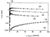
OLED는 다음과 같이 제조하였다. 애노드 기판으로서 사용된 예비-패턴화한 ITO 코팅 유리를 10분 동안 UV-오존으로 세정하였다. 이어서, 방사-코팅을 이용하여 바이엘 코포레이션사로부터 입수된 [폴리(3,4)-에틸렌다이옥시싸이오펜/폴리스타이렌 설포네이트](PEDOT/PSS) 중합체 층(60nm)를 ITO의 상부에 증착시킨 다음, (24℃의 실온 및 62%의 상대습도를 가진) 주변 환경에서 1시간 동안 180℃에서 베이킹하였다. 이어서, 샘플들을 동일한 글로브박스내로 이동시켰다. 추가적으로 특정되지 않는 한은, 동일한 글로브박스내에서 하기의 단계들을 실시하였다. 다음으로, OPA9903:SR454로 이루어진 발광층을 p-자일렌중 그의 용액으로부터 PEDOT/PSS 층의 상부에 방사-코팅한 다음, UV 램프(미국 캘리포니아 91796 업랜드에 소재한 울트라바이올렛 프로덕츠(Ultraviolet Products)사로부터 입수된, 필터가 제거된 R-52 그리드 램프)(약 310nm, 365nm 및400nm에서 측정된 강도는 0.39, 0.43 및 1.93 mW/㎠였다)를 사용하여 1분 동안 경화하였다. 다음으로, OPA9903:Ba-TPCP의 혼합물 층을 경화된 발광층상에 방사-코팅한 다음, 약 180℃에서 약 15분 동안 베이킹하였다. 마지막으로, Al의 층(약 110nm)을 OPA9903:Ba-TPCP 층의 상부에서 섀도 마스크를 통하여 열적으로 증발시켰다. 금속이 증발한 다음에, 광학 접착제인 노랜드 68(Norland 68)로 밀봉된 유리 슬라이드를 사용하여 디바이스를 캡슐화하였다. 활성 영역은 약 0.2㎠이다.OLEDs were prepared as follows. The pre-patterned ITO coated glass used as anode substrate was washed with UV-ozone for 10 minutes. Subsequently, a [poly (3,4) -ethylenedioxythiophene / polystyrene sulfonate] (PEDOT / PSS) polymer layer (60 nm) obtained from Bayer Corporation was then deposited on top of ITO using spin-coating. , Baked at 180 ° C. for 1 hour in an ambient environment (with room temperature of 24 ° C. and relative humidity of 62%). The samples were then moved into the same glovebox. Unless otherwise specified, the following steps were carried out in the same glovebox. Next, a light emitting layer consisting of OPA9903: SR454 was spin-coated on top of the PEDOT / PSS layer from its solution in p-xylene and then UV lamp (Ultraviolet Products, Upland, 91796, USA). Cured for 1 minute using a filter-free R-52 grid lamp obtained (measured at about 310 nm, 365 nm and 400 nm were 0.39, 0.43 and 1.93 mW / cm 2). Next, a mixture layer of OPA9903: Ba-TPCP was spin-coated on the cured light emitting layer and then baked at about 180 ° C. for about 15 minutes. Finally, a layer of Al (about 110 nm) was thermally evaporated through a shadow mask on top of the OPA9903: Ba-TPCP layer. After the metal had evaporated, the device was encapsulated using a glass slide sealed with
4개의 OLED 디바이스를 제조하였다. 대조용 디바이스인 디바이스 G는 OPA9903:Ba-TPCP의 혼합물 층을 갖지 않았다. 디바이스 H, I 및 J는 Al 증착전에 OPA9903:Ba-TPCP의 혼합물 층을 서로 다른 방법으로 처리하였다는 것을 제외하고는 동일한 구조를 가졌다. 디바이스 H의 경우, 혼합물 층을 방사-코팅된 상태로 약 3분 동안 주변 환경에 노출시킨 다음, 동일한 글로브박스내에서 약 15분 동안 180℃에서 베이킹하였다. 디바이스 I의 경우에는, 혼합물 층을 주변 환경에 노출시키지 않았으며, 디바이스 J의 경우에는, 혼합물 층을 베이킹 단계를 실시한 후에 3분 동안 주변 환경에 노출시켰다. 도 26은 디바이스 G, H, I 및 J에 대한 효율(cd/A) 대 전류밀도(mA/㎠)의 관계를 나타낸 도면이다.Four OLED devices were manufactured. The control device, Device G, did not have a mixture layer of OPA9903: Ba-TPCP. Devices H, I and J had the same structure, except that the mixture layers of OPA9903: Ba-TPCP were treated in different ways prior to Al deposition. For device H, the mixture layer was exposed to the surrounding environment for about 3 minutes in a spin-coated state and then baked at 180 ° C. for about 15 minutes in the same glovebox. In the case of device I, the mixture layer was not exposed to the surrounding environment and in the case of device J, the mixture layer was exposed to the surrounding environment for three minutes after the baking step was carried out. FIG. 26 shows the relationship between efficiency (cd / A) versus current density (mA / cm 2) for devices G, H, I, and J. FIG.
효율(130) 대 전류밀도(132) 곡선을 비교한 결과, 디바이스 H(곡선 136), I(곡선 140) 및 J(곡선 138)에서와 같이 OPA9903:Ba-TPCP의 혼합물 층을 도입하면 대조용 디바이스 G(곡선 134)에 비해 디바이스 효율이 상당히 개선되었음을 나타낸다. 4개의 디바이스는 모두 동일한 애노드를 공유하기 때문에, 효율에 있어서 관찰된 개선 효과는 처리되지 않은 Al 캐소드의 활성에 직접적으로 영향을 미치는 것으로 생각된다. 더욱이, 상기 도면은 또한 베이킹하고 주변 환경에 노출시키는 순서도 또한 중요함을 보여준다. 주변 환경에 노출시키지 않은 디바이스 I는 디바이스 H 및 J에 비해 최상으로 개선된 것으로 나타났다. 주변 환경에 노출시킨 다음 베이킹 단계를 실시한 디바이스 H는 베이킹 단계를 실시한 후에 주변 환경에 노출시킨 디바이스 J에 비해 더 양호한 효율을 나타낸다.Comparing the
출원인들은 특정 이론으로 국한시키려는 것은 아니지만, 베이킹 (및/또는 다른 잠재적인 수단)시에 바륨 화합물(Ba-TPCP)이 분해하여 결과적으로는 활성 중합체(OPA9903)를 활성화시킬 수 있는 유리 바륨 원자를 방출하는 것으로 생각된다. 하기 반응식(5)은 알칼리토금속 유기금속성 화합물 M-TPCP(여기서, M은 바륨을 비롯한 알칼리토금속이다)이 가열시에 분해되어 유리 금속원자를 방출하는 관계를 나타낸 것이다:Applicants do not intend to be bound by a particular theory, but upon baking (and / or other potential means) the barium compound (Ba-TPCP) decomposes, releasing free barium atoms that can eventually activate the active polymer (OPA9903). I think. Scheme (5) shows the relationship of the alkaline earth metal organometallic compound M-TPCP, where M is an alkaline earth metal including barium, to decompose upon heating to release free metal atoms:

활성화된 OPA9903은 처리되지 않은 Al 캐소드에서 OPA9903의 활성층내로의 전자 주입을 촉진한다.Activated OPA9903 promotes the injection of electrons into the active layer of OPA9903 in the untreated Al cathode.
본 발명의 상술된 많은 실시태양은 큰 전도도를 갖는 OLED 디바이스를 제공함으로써 OLED 발광효율을 증가시킬 수 있는 등의 많은 잇점을 갖는다.Many of the above-described embodiments of the present invention have many advantages, such as being able to increase OLED luminous efficiency by providing OLED devices with large conductivity.
지금까지 본 발명의 단지 몇 가지 특징을 예시하고 설명하였지만, 당업자는 많은 변경 및 변화를 행할 수 있을 것이다. 따라서, 첨부된 특허청구의 범위는 본 발명의 범주내에 속하는 그러한 모든 변경 및 변화를 포함하는 것으로 이해되어야 한다.While only some features of the invention have been illustrated and described so far, those skilled in the art will be able to make many changes and variations. Accordingly, it is to be understood that the appended claims cover all such modifications and variations as fall within the scope of the present invention.
Claims (42)
Applications Claiming Priority (2)
| Application Number | Priority Date | Filing Date | Title |
|---|---|---|---|
| US11/243,194 US20070077452A1 (en) | 2005-10-04 | 2005-10-04 | Organic light emitting devices having latent activated layers and methods of fabricating the same |
| US11/243,194 | 2005-10-04 |
Publications (1)
| Publication Number | Publication Date |
|---|---|
| KR20080063764A true KR20080063764A (en) | 2008-07-07 |
Family
ID=37401542
Family Applications (1)
| Application Number | Title | Priority Date | Filing Date |
|---|---|---|---|
| KR1020087008127A KR20080063764A (en) | 2005-10-04 | 2006-07-20 | Organic light emitting devices having latent activated layers and methods of fabricating the same |
Country Status (7)
| Country | Link |
|---|---|
| US (2) | US20070077452A1 (en) |
| EP (1) | EP1935042A1 (en) |
| JP (1) | JP2009510795A (en) |
| KR (1) | KR20080063764A (en) |
| CN (1) | CN101283462B (en) |
| TW (1) | TW200721563A (en) |
| WO (1) | WO2007040728A1 (en) |
Families Citing this family (12)
| Publication number | Priority date | Publication date | Assignee | Title |
|---|---|---|---|---|
| US20070075628A1 (en) * | 2005-10-04 | 2007-04-05 | General Electric Company | Organic light emitting devices having latent activated layers |
| JP5261028B2 (en) * | 2007-08-21 | 2013-08-14 | 富士フイルム株式会社 | Display element |
| WO2009126918A1 (en) * | 2008-04-11 | 2009-10-15 | Plextronics, Inc. | Doped conjugated polymers, devices, and methods of making devices |
| US20090284158A1 (en) * | 2008-05-16 | 2009-11-19 | General Electric Company | Organic light emitting device based lighting for low cost, flexible large area signage |
| WO2009142763A1 (en) * | 2008-05-23 | 2009-11-26 | Swaminathan Ramesh | Hybrid photovoltaic cell module |
| US8022623B2 (en) * | 2008-08-15 | 2011-09-20 | General Electric Company | Ultra-thin multi-substrate color tunable OLED device |
| US20110008525A1 (en) * | 2009-07-10 | 2011-01-13 | General Electric Company | Condensation and curing of materials within a coating system |
| JP6035706B2 (en) | 2010-04-09 | 2016-11-30 | 三菱化学株式会社 | Manufacturing method of composition for organic electric field element, composition for organic electric field element, manufacturing method of organic electroluminescent element, organic electroluminescent element, organic EL display device and organic EL lighting |
| KR101562859B1 (en) * | 2014-04-02 | 2015-10-27 | 한국생산기술연구원 | Conductive plastic layer using photoacid generator and method for manufacturing thereof and forming method of pattern on the same |
| TWI579492B (en) * | 2015-05-11 | 2017-04-21 | 綠點高新科技股份有限公司 | Manufacturing method of a lamp and the lamp |
| CN104952908B (en) * | 2015-07-01 | 2018-12-21 | 上海和辉光电有限公司 | A kind of OLED display panel and preparation method thereof |
| JP7310609B2 (en) * | 2017-12-20 | 2023-07-19 | 日産化学株式会社 | charge transport varnish |
Family Cites Families (23)
| Publication number | Priority date | Publication date | Assignee | Title |
|---|---|---|---|---|
| US5198153A (en) * | 1989-05-26 | 1993-03-30 | International Business Machines Corporation | Electrically conductive polymeric |
| US5200112A (en) * | 1989-05-26 | 1993-04-06 | International Business Machines Corporation | Electrically conductive polymeric materials and uses thereof |
| US5650261A (en) * | 1989-10-27 | 1997-07-22 | Rohm And Haas Company | Positive acting photoresist comprising a photoacid, a photobase and a film forming acid-hardening resin system |
| US5514878A (en) * | 1994-03-18 | 1996-05-07 | Holmes; Andrew B. | Polymers for electroluminescent devices |
| US5719467A (en) * | 1995-07-27 | 1998-02-17 | Hewlett-Packard Company | Organic electroluminescent device |
| US5965280A (en) * | 1997-03-03 | 1999-10-12 | Hewlett-Packard Company | Patterned polymer electroluminescent devices based on microlithographic processes |
| GB9718393D0 (en) * | 1997-08-29 | 1997-11-05 | Cambridge Display Tech Ltd | Electroluminescent Device |
| US6045977A (en) * | 1998-02-19 | 2000-04-04 | Lucent Technologies Inc. | Process for patterning conductive polyaniline films |
| GB9815271D0 (en) * | 1998-07-14 | 1998-09-09 | Cambridge Display Tech Ltd | Particles and devices comprising particles |
| SG78412A1 (en) * | 1999-03-31 | 2001-02-20 | Ciba Sc Holding Ag | Oxime derivatives and the use thereof as latent acids |
| NL1014545C2 (en) * | 1999-03-31 | 2002-02-26 | Ciba Sc Holding Ag | Oxim derivatives and their use as latent acids. |
| AU3977900A (en) * | 1999-04-06 | 2000-10-23 | Cambridge Display Technology Limited | Method for doping a polymer |
| CN1084134C (en) * | 1999-08-25 | 2002-05-01 | 吉林大学 | Electroluminescent device for reversible generation and removal of images by light radiation |
| TWI272451B (en) * | 2000-09-25 | 2007-02-01 | Ciba Sc Holding Ag | Chemically amplified photoresist composition, process for preparation of a photoresist, and use of said chemically amplified photoresist composition |
| DE60133929D1 (en) * | 2000-12-04 | 2008-06-19 | Ciba Holding Inc | ONIUM SALT AND ITS USE AS LATENT ACIDS |
| JP4408220B2 (en) * | 2001-06-01 | 2010-02-03 | チバ ホールディング インコーポレーテッド | Substituted oxime derivatives and their use as latent acids |
| JP2003017269A (en) * | 2001-06-29 | 2003-01-17 | Toshiba Corp | Organic electroluminescent display element and its manufacturing method |
| EP1423991A4 (en) * | 2001-07-27 | 2009-06-17 | Univ Ohio State | Methods for fabricating polymer light emitting devices by lamination |
| US8932730B2 (en) * | 2002-04-08 | 2015-01-13 | The University of Northern California | Doped organic carrier transport materials |
| CN100367113C (en) * | 2002-12-11 | 2008-02-06 | 三星电子株式会社 | Composition for forming conjugated polymer pattern and method for forming conjugated polymer pattern using the same composition |
| JP4554329B2 (en) * | 2004-06-02 | 2010-09-29 | 大日本印刷株式会社 | Organic electronic device and method of manufacturing organic electronic device |
| US8026510B2 (en) * | 2004-10-20 | 2011-09-27 | Dai Nippon Printing Co., Ltd. | Organic electronic device and method for producing the same |
| US7510951B2 (en) * | 2005-05-12 | 2009-03-31 | Lg Chem, Ltd. | Method for forming high-resolution pattern with direct writing means |
-
2005
- 2005-10-04 US US11/243,194 patent/US20070077452A1/en not_active Abandoned
-
2006
- 2006-07-20 KR KR1020087008127A patent/KR20080063764A/en active IP Right Grant
- 2006-07-20 EP EP06788152A patent/EP1935042A1/en not_active Withdrawn
- 2006-07-20 WO PCT/US2006/028428 patent/WO2007040728A1/en active Application Filing
- 2006-07-20 CN CN2006800372987A patent/CN101283462B/en not_active Expired - Fee Related
- 2006-07-20 JP JP2008534519A patent/JP2009510795A/en active Pending
- 2006-08-04 TW TW095128750A patent/TW200721563A/en unknown
-
2010
- 2010-05-26 US US12/787,911 patent/US20100230829A1/en not_active Abandoned
Also Published As
| Publication number | Publication date |
|---|---|
| US20070077452A1 (en) | 2007-04-05 |
| CN101283462B (en) | 2011-08-24 |
| WO2007040728A1 (en) | 2007-04-12 |
| US20100230829A1 (en) | 2010-09-16 |
| EP1935042A1 (en) | 2008-06-25 |
| JP2009510795A (en) | 2009-03-12 |
| TW200721563A (en) | 2007-06-01 |
| CN101283462A (en) | 2008-10-08 |
Similar Documents
| Publication | Publication Date | Title |
|---|---|---|
| KR20080063764A (en) | Organic light emitting devices having latent activated layers and methods of fabricating the same | |
| KR101434867B1 (en) | Organic light emitting devices having latent activated layers | |
| US7368659B2 (en) | Electrodes mitigating effects of defects in organic electronic devices | |
| JP5312949B2 (en) | Laminated electrode for electroactive device and method for producing the same | |
| TWI499105B (en) | Organic optoelectronic device and method for manufacturing the same | |
| KR101261633B1 (en) | Metal compound-metal multilayer electrodes for organic electronic devices | |
| KR20110052688A (en) | Method of manufacture of a multi-layer phosphorescent organic light emitting device, and articles thereof | |
| WO2004021463A2 (en) | Buffer layers for organic electroluminescent devices and methods of manufacture and use | |
| WO2005029607A1 (en) | Compound electrodes for electronic devices | |
| KR20080045242A (en) | Organic electro-luminescence element, production method and use thereof | |
| KR101039922B1 (en) | Method for fabricating white organic light emitting device utilizing porous polymer light emitting layer and white organic light emitting device fabricated thereby |
Legal Events
| Date | Code | Title | Description |
|---|---|---|---|
| A201 | Request for examination | ||
| E701 | Decision to grant or registration of patent right |