KR20070090035A - Force sensing membrane - Google Patents
Force sensing membrane Download PDFInfo
- Publication number
- KR20070090035A KR20070090035A KR1020077016976A KR20077016976A KR20070090035A KR 20070090035 A KR20070090035 A KR 20070090035A KR 1020077016976 A KR1020077016976 A KR 1020077016976A KR 20077016976 A KR20077016976 A KR 20077016976A KR 20070090035 A KR20070090035 A KR 20070090035A
- Authority
- KR
- South Korea
- Prior art keywords
- force sensing
- conductor
- sensing membrane
- particles
- membrane
- Prior art date
Links
- 239000012528 membrane Substances 0.000 title claims abstract description 88
- 239000002245 particle Substances 0.000 claims abstract description 160
- 239000004020 conductor Substances 0.000 claims abstract description 118
- 239000002131 composite material Substances 0.000 claims abstract description 39
- 230000004044 response Effects 0.000 claims abstract description 20
- 229920001971 elastomer Polymers 0.000 claims description 56
- 239000000806 elastomer Substances 0.000 claims description 53
- 239000013536 elastomeric material Substances 0.000 claims description 43
- 239000011810 insulating material Substances 0.000 claims description 15
- 238000000034 method Methods 0.000 claims description 14
- 230000008859 change Effects 0.000 claims description 9
- 239000000758 substrate Substances 0.000 claims description 9
- 239000011521 glass Substances 0.000 claims description 7
- 229910052751 metal Inorganic materials 0.000 claims description 7
- 239000002184 metal Substances 0.000 claims description 7
- 239000011248 coating agent Substances 0.000 claims description 5
- 238000000576 coating method Methods 0.000 claims description 5
- 239000000835 fiber Substances 0.000 claims description 4
- 239000000945 filler Substances 0.000 claims description 4
- 229910052710 silicon Inorganic materials 0.000 claims description 3
- 239000010703 silicon Substances 0.000 claims description 3
- 229920006132 styrene block copolymer Polymers 0.000 claims description 3
- 229920001400 block copolymer Polymers 0.000 claims description 2
- 229920005996 polystyrene-poly(ethylene-butylene)-polystyrene Polymers 0.000 claims description 2
- 239000007771 core particle Substances 0.000 claims 3
- 238000001514 detection method Methods 0.000 claims 2
- 229920000346 polystyrene-polyisoprene block-polystyrene Polymers 0.000 claims 1
- 238000003825 pressing Methods 0.000 claims 1
- 229920005573 silicon-containing polymer Polymers 0.000 claims 1
- 239000010410 layer Substances 0.000 description 71
- 239000000463 material Substances 0.000 description 24
- XLYOFNOQVPJJNP-UHFFFAOYSA-N water Chemical compound O XLYOFNOQVPJJNP-UHFFFAOYSA-N 0.000 description 16
- 230000004913 activation Effects 0.000 description 10
- 238000012360 testing method Methods 0.000 description 9
- 238000009826 distribution Methods 0.000 description 8
- RYGMFSIKBFXOCR-UHFFFAOYSA-N Copper Chemical compound [Cu] RYGMFSIKBFXOCR-UHFFFAOYSA-N 0.000 description 7
- -1 inverters Substances 0.000 description 7
- 239000011324 bead Substances 0.000 description 6
- 239000000203 mixture Substances 0.000 description 6
- 229920000728 polyester Polymers 0.000 description 6
- 208000004210 Pressure Ulcer Diseases 0.000 description 5
- VYPSYNLAJGMNEJ-UHFFFAOYSA-N Silicium dioxide Chemical compound O=[Si]=O VYPSYNLAJGMNEJ-UHFFFAOYSA-N 0.000 description 5
- 239000011889 copper foil Substances 0.000 description 5
- 230000035945 sensitivity Effects 0.000 description 5
- 230000008901 benefit Effects 0.000 description 4
- 239000006260 foam Substances 0.000 description 4
- AMGQUBHHOARCQH-UHFFFAOYSA-N indium;oxotin Chemical compound [In].[Sn]=O AMGQUBHHOARCQH-UHFFFAOYSA-N 0.000 description 4
- 238000004519 manufacturing process Methods 0.000 description 4
- 229920000642 polymer Polymers 0.000 description 4
- 229920001296 polysiloxane Polymers 0.000 description 4
- 229920002379 silicone rubber Polymers 0.000 description 4
- 229920001940 conductive polymer Polymers 0.000 description 3
- 238000001723 curing Methods 0.000 description 3
- 235000013870 dimethyl polysiloxane Nutrition 0.000 description 3
- 239000011888 foil Substances 0.000 description 3
- 238000011068 loading method Methods 0.000 description 3
- 150000002739 metals Chemical class 0.000 description 3
- 238000012986 modification Methods 0.000 description 3
- 230000004048 modification Effects 0.000 description 3
- 238000012544 monitoring process Methods 0.000 description 3
- 239000003921 oil Substances 0.000 description 3
- BASFCYQUMIYNBI-UHFFFAOYSA-N platinum Chemical compound [Pt] BASFCYQUMIYNBI-UHFFFAOYSA-N 0.000 description 3
- 229920000435 poly(dimethylsiloxane) Polymers 0.000 description 3
- 229920000768 polyamine Polymers 0.000 description 3
- 229920005862 polyol Polymers 0.000 description 3
- 239000005060 rubber Substances 0.000 description 3
- 239000004065 semiconductor Substances 0.000 description 3
- 239000004945 silicone rubber Substances 0.000 description 3
- 239000007787 solid Substances 0.000 description 3
- 229920001187 thermosetting polymer Polymers 0.000 description 3
- KAKZBPTYRLMSJV-UHFFFAOYSA-N Butadiene Chemical compound C=CC=C KAKZBPTYRLMSJV-UHFFFAOYSA-N 0.000 description 2
- 206010011985 Decubitus ulcer Diseases 0.000 description 2
- 208000008960 Diabetic foot Diseases 0.000 description 2
- XUIMIQQOPSSXEZ-UHFFFAOYSA-N Silicon Chemical compound [Si] XUIMIQQOPSSXEZ-UHFFFAOYSA-N 0.000 description 2
- 150000001252 acrylic acid derivatives Chemical class 0.000 description 2
- 230000005540 biological transmission Effects 0.000 description 2
- 239000003054 catalyst Substances 0.000 description 2
- 238000006243 chemical reaction Methods 0.000 description 2
- 229910052802 copper Inorganic materials 0.000 description 2
- 239000010949 copper Substances 0.000 description 2
- 230000007423 decrease Effects 0.000 description 2
- 230000000694 effects Effects 0.000 description 2
- 230000005684 electric field Effects 0.000 description 2
- 238000004049 embossing Methods 0.000 description 2
- 239000012948 isocyanate Substances 0.000 description 2
- 238000012417 linear regression Methods 0.000 description 2
- 229910044991 metal oxide Inorganic materials 0.000 description 2
- 150000004706 metal oxides Chemical class 0.000 description 2
- 239000004005 microsphere Substances 0.000 description 2
- 229920003023 plastic Polymers 0.000 description 2
- 239000004033 plastic Substances 0.000 description 2
- 239000002985 plastic film Substances 0.000 description 2
- 229920006267 polyester film Polymers 0.000 description 2
- 229920000570 polyether Polymers 0.000 description 2
- 229920001228 polyisocyanate Polymers 0.000 description 2
- 239000005056 polyisocyanate Substances 0.000 description 2
- 229920000098 polyolefin Polymers 0.000 description 2
- 150000003077 polyols Chemical class 0.000 description 2
- 239000000377 silicon dioxide Substances 0.000 description 2
- 230000005236 sound signal Effects 0.000 description 2
- SKRWFPLZQAAQSU-UHFFFAOYSA-N stibanylidynetin;hydrate Chemical compound O.[Sn].[Sb] SKRWFPLZQAAQSU-UHFFFAOYSA-N 0.000 description 2
- 230000000007 visual effect Effects 0.000 description 2
- VSKJLJHPAFKHBX-UHFFFAOYSA-N 2-methylbuta-1,3-diene;styrene Chemical compound CC(=C)C=C.C=CC1=CC=CC=C1.C=CC1=CC=CC=C1 VSKJLJHPAFKHBX-UHFFFAOYSA-N 0.000 description 1
- NLHHRLWOUZZQLW-UHFFFAOYSA-N Acrylonitrile Chemical compound C=CC#N NLHHRLWOUZZQLW-UHFFFAOYSA-N 0.000 description 1
- OKTJSMMVPCPJKN-UHFFFAOYSA-N Carbon Chemical compound [C] OKTJSMMVPCPJKN-UHFFFAOYSA-N 0.000 description 1
- 239000004971 Cross linker Substances 0.000 description 1
- 239000004593 Epoxy Substances 0.000 description 1
- 239000004606 Fillers/Extenders Substances 0.000 description 1
- 239000013032 Hydrocarbon resin Substances 0.000 description 1
- 239000004712 Metallocene polyethylene (PE-MC) Substances 0.000 description 1
- UFWIBTONFRDIAS-UHFFFAOYSA-N Naphthalene Chemical compound C1=CC=CC2=CC=CC=C21 UFWIBTONFRDIAS-UHFFFAOYSA-N 0.000 description 1
- 239000004952 Polyamide Substances 0.000 description 1
- 239000005062 Polybutadiene Substances 0.000 description 1
- 229920002367 Polyisobutene Polymers 0.000 description 1
- 239000004721 Polyphenylene oxide Substances 0.000 description 1
- 239000004793 Polystyrene Substances 0.000 description 1
- 229920002396 Polyurea Polymers 0.000 description 1
- 206010040943 Skin Ulcer Diseases 0.000 description 1
- 239000004433 Thermoplastic polyurethane Substances 0.000 description 1
- 208000025865 Ulcer Diseases 0.000 description 1
- 238000005054 agglomeration Methods 0.000 description 1
- 230000004931 aggregating effect Effects 0.000 description 1
- 230000002776 aggregation Effects 0.000 description 1
- HSFWRNGVRCDJHI-UHFFFAOYSA-N alpha-acetylene Natural products C#C HSFWRNGVRCDJHI-UHFFFAOYSA-N 0.000 description 1
- 150000001412 amines Chemical class 0.000 description 1
- 238000000418 atomic force spectrum Methods 0.000 description 1
- 238000009530 blood pressure measurement Methods 0.000 description 1
- 229920005549 butyl rubber Polymers 0.000 description 1
- 229910052799 carbon Inorganic materials 0.000 description 1
- 125000003178 carboxy group Chemical group [H]OC(*)=O 0.000 description 1
- 239000000919 ceramic Substances 0.000 description 1
- 239000003795 chemical substances by application Substances 0.000 description 1
- 239000011247 coating layer Substances 0.000 description 1
- 238000001816 cooling Methods 0.000 description 1
- 229920006037 cross link polymer Polymers 0.000 description 1
- 206010012601 diabetes mellitus Diseases 0.000 description 1
- LDCRTTXIJACKKU-ARJAWSKDSA-N dimethyl maleate Chemical group COC(=O)\C=C/C(=O)OC LDCRTTXIJACKKU-ARJAWSKDSA-N 0.000 description 1
- 239000004205 dimethyl polysiloxane Substances 0.000 description 1
- 201000010099 disease Diseases 0.000 description 1
- 208000037265 diseases, disorders, signs and symptoms Diseases 0.000 description 1
- 239000006185 dispersion Substances 0.000 description 1
- 125000003700 epoxy group Chemical group 0.000 description 1
- 150000002148 esters Chemical class 0.000 description 1
- LYCAIKOWRPUZTN-UHFFFAOYSA-N ethylene glycol Natural products OCCO LYCAIKOWRPUZTN-UHFFFAOYSA-N 0.000 description 1
- 230000001747 exhibiting effect Effects 0.000 description 1
- YMTINGFKWWXKFG-UHFFFAOYSA-N fenofibrate Chemical compound C1=CC(OC(C)(C)C(=O)OC(C)C)=CC=C1C(=O)C1=CC=C(Cl)C=C1 YMTINGFKWWXKFG-UHFFFAOYSA-N 0.000 description 1
- 229920002457 flexible plastic Polymers 0.000 description 1
- 229910021485 fumed silica Inorganic materials 0.000 description 1
- 239000003365 glass fiber Substances 0.000 description 1
- PCHJSUWPFVWCPO-UHFFFAOYSA-N gold Chemical compound [Au] PCHJSUWPFVWCPO-UHFFFAOYSA-N 0.000 description 1
- 229910052737 gold Inorganic materials 0.000 description 1
- 239000010931 gold Substances 0.000 description 1
- 229920006270 hydrocarbon resin Polymers 0.000 description 1
- 125000002887 hydroxy group Chemical group [H]O* 0.000 description 1
- WGCNASOHLSPBMP-UHFFFAOYSA-N hydroxyacetaldehyde Natural products OCC=O WGCNASOHLSPBMP-UHFFFAOYSA-N 0.000 description 1
- 239000011256 inorganic filler Substances 0.000 description 1
- 229910003475 inorganic filler Inorganic materials 0.000 description 1
- 229910010272 inorganic material Inorganic materials 0.000 description 1
- 239000011147 inorganic material Substances 0.000 description 1
- 238000009413 insulation Methods 0.000 description 1
- 230000001788 irregular Effects 0.000 description 1
- 150000002736 metal compounds Chemical class 0.000 description 1
- 229910001092 metal group alloy Inorganic materials 0.000 description 1
- 239000002923 metal particle Substances 0.000 description 1
- 229920003052 natural elastomer Polymers 0.000 description 1
- 229920001194 natural rubber Polymers 0.000 description 1
- 239000012766 organic filler Substances 0.000 description 1
- 239000011368 organic material Substances 0.000 description 1
- 238000004806 packaging method and process Methods 0.000 description 1
- 239000013618 particulate matter Substances 0.000 description 1
- 239000012466 permeate Substances 0.000 description 1
- 238000000016 photochemical curing Methods 0.000 description 1
- 229920006255 plastic film Polymers 0.000 description 1
- 239000002984 plastic foam Substances 0.000 description 1
- 239000004014 plasticizer Substances 0.000 description 1
- 229910052697 platinum Inorganic materials 0.000 description 1
- 229920001084 poly(chloroprene) Polymers 0.000 description 1
- 229920001197 polyacetylene Polymers 0.000 description 1
- 229920002647 polyamide Polymers 0.000 description 1
- 229920000767 polyaniline Polymers 0.000 description 1
- 229920002857 polybutadiene Polymers 0.000 description 1
- 229920000647 polyepoxide Polymers 0.000 description 1
- 229920005906 polyester polyol Polymers 0.000 description 1
- 229920001195 polyisoprene Polymers 0.000 description 1
- 229920000128 polypyrrole Polymers 0.000 description 1
- 229920002223 polystyrene Polymers 0.000 description 1
- 150000003097 polyterpenes Chemical class 0.000 description 1
- 229920000123 polythiophene Polymers 0.000 description 1
- 229920002635 polyurethane Polymers 0.000 description 1
- 239000004814 polyurethane Substances 0.000 description 1
- 239000000843 powder Substances 0.000 description 1
- 230000002265 prevention Effects 0.000 description 1
- 238000012545 processing Methods 0.000 description 1
- 239000000047 product Substances 0.000 description 1
- 239000012858 resilient material Substances 0.000 description 1
- 230000035807 sensation Effects 0.000 description 1
- 230000001953 sensory effect Effects 0.000 description 1
- 238000000926 separation method Methods 0.000 description 1
- 231100000019 skin ulcer Toxicity 0.000 description 1
- 125000006850 spacer group Chemical group 0.000 description 1
- 238000003860 storage Methods 0.000 description 1
- 229920003048 styrene butadiene rubber Polymers 0.000 description 1
- 239000000126 substance Substances 0.000 description 1
- 229920003051 synthetic elastomer Polymers 0.000 description 1
- 239000005061 synthetic rubber Substances 0.000 description 1
- 238000010345 tape casting Methods 0.000 description 1
- 238000001029 thermal curing Methods 0.000 description 1
- 229920001169 thermoplastic Polymers 0.000 description 1
- 229920002803 thermoplastic polyurethane Polymers 0.000 description 1
- 239000004416 thermosoftening plastic Substances 0.000 description 1
- 229940055755 tricor Drugs 0.000 description 1
- 231100000397 ulcer Toxicity 0.000 description 1
- 150000003673 urethanes Chemical class 0.000 description 1
- 125000000391 vinyl group Chemical group [H]C([*])=C([H])[H] 0.000 description 1
- 229920002554 vinyl polymer Polymers 0.000 description 1
Images


Classifications
-
- G—PHYSICS
- G01—MEASURING; TESTING
- G01L—MEASURING FORCE, STRESS, TORQUE, WORK, MECHANICAL POWER, MECHANICAL EFFICIENCY, OR FLUID PRESSURE
- G01L1/00—Measuring force or stress, in general
- G01L1/20—Measuring force or stress, in general by measuring variations in ohmic resistance of solid materials or of electrically-conductive fluids; by making use of electrokinetic cells, i.e. liquid-containing cells wherein an electrical potential is produced or varied upon the application of stress
-
- H—ELECTRICITY
- H01—ELECTRIC ELEMENTS
- H01H—ELECTRIC SWITCHES; RELAYS; SELECTORS; EMERGENCY PROTECTIVE DEVICES
- H01H1/00—Contacts
- H01H1/02—Contacts characterised by the material thereof
- H01H1/021—Composite material
- H01H1/029—Composite material comprising conducting material dispersed in an elastic support or binding material
Abstract
Description
본 발명은 힘 감지 막, 이 막을 포함하는 장치, 및 상기 힘 감지 막을 사용하여 힘을 감지하는 방법에 관한 것이다.The present invention relates to a force sensing membrane, a device comprising the membrane, and a method of sensing force using the force sensing membrane.
힘 감지 막은 접촉/터치(contact/touch)를 탐지하거나, 힘 또는 가해진 하중의 상대적 변화를 탐지 및 측정하거나, 힘의 변화 속도를 탐지 및 측정하고/하거나 힘 또는 하중의 제거를 탐지하기 위한 다양한 응용 분야에 사용된다.Force sensing membranes are used in various applications for detecting contacts / touch, detecting and measuring relative changes in force or applied load, detecting and measuring the rate of change of force, and / or detecting the removal of force or load. Used in the field
힘 감지 막은 통상 두 개의 전도성 접촉부(conducting contact) 사이에 배치된 전도성 입자를 포함하는 엘라스토머 ("엘라스토머 층")로 구성된다. 압력이 전도성 접촉부 중의 하나에 가해질 때, 전도성 접촉부는 엘라스토머 층의 표면에 대해 압착되고, 전도 경로가 생성된다. 전도 경로는 엘라스토머를 통해 굽은 경로를 만드는 전도성 입자 쇄로 이루어진다. 그러므로, 엘라스토머 중의 전도성 입자의 농도는 연속 경로를 만들기 위해서는 특정 역치 이상 (즉, 삼출 역치 이상)이어야 한다. 압력이 증가함에 따라, 전도성 접촉부와 엘라스토머 층의 표면 사이에 더 많은 접촉 회수와 영역이 생성된다. 따라서, 엘라스토머와 전도성 입자를 통한 더 많은 수의 전도 경로가 생성되고, 엘라스토머 층을 가로지르는 저항이 감소된다.The force sensing membrane is usually composed of an elastomer ("elastomer layer") comprising conductive particles disposed between two conductive contacts. When pressure is applied to one of the conductive contacts, the conductive contacts are pressed against the surface of the elastomeric layer and a conductive path is created. The conductive path consists of conductive particle chains that make a curved path through the elastomer. Therefore, the concentration of conductive particles in the elastomer must be above a certain threshold (ie, above the effusion threshold) in order to create a continuous path. As the pressure increases, more contact counts and areas are created between the conductive contacts and the surface of the elastomer layer. Thus, a larger number of conductive paths through the elastomer and the conductive particles are created, and the resistance across the elastomer layer is reduced.
발명의 개요Summary of the Invention
상기 사항을 고려하여, 본 발명자들은 종래 기술의 힘 감지 막의 전도 경로가 다수의 전도성 입자 접촉으로 이루어지기 때문에 저항과 이력 현상(hysteresis)에 변이가 발생할 수 있음을 인지하였다.In view of the above, the inventors have recognized that variations in resistance and hysteresis can occur because the conduction path of the force sensing membrane of the prior art is made of a plurality of conductive particle contacts.
간단히 말하면, 일 측면으로 본 발명은 전도성 입자의 농도가 삼출 역치보다 더 낮고 실질적으로 모든 전도 경로가 단일 입자를 통과하는 힘 감지 막을 제공한다. 힘 감지 막은 (a) 제2 전도체를 향해 이동 가능한 제1 전도체, (b) 제2 전도체, (c) 제1 전도체와 제2 전도체 사이의 충분한 압력의 인가 하에 배치된 두 전도체를 전기적으로 연결하도록 복합 재료, 및 (d) 힘 감지 막을 가로질러 동적 전기 응답(dynamic electrical response)(예컨대, 저항, 컨덕턴스, 전류, 전압 등)을 측정하는 수단을 포함한다. 본 명세서에 사용된 "'동적' 전기 응답을 측정하는 수단"은 단순히 비작동/작동 그 이상을 측정하는 전기 응답을 측정하는 모든 수단을 포함한다.In short, in one aspect, the present invention provides a force sensing membrane in which the concentration of conductive particles is lower than the effusion threshold and substantially all the conductive paths pass through a single particle. The force sensing membrane is configured to electrically connect two conductors disposed under application of sufficient pressure between (a) a first conductor movable toward the second conductor, (b) a second conductor, and (c) a sufficient pressure between the first and second conductors. Composite material, and (d) means for measuring a dynamic electrical response (eg, resistance, conductance, current, voltage, etc.) across the force sensing film. As used herein, "means for measuring the 'dynamic' electrical response" includes all means for measuring the electrical response that simply measures non-operational / operational.
상기 복합 재료는 엘라스토머 층에 적어도 부분적으로 매립된 전도성 입자를 포함한다. 전도성 입자는 상대적 배향(relative orientation)이 없으며, 제1 전도체와 제2 전도체 사이에 이루어진 거의 모든 전기적 연결(electrical connection)이 z 방향에서 존재하도록 (즉, 거의 모든 전기적 연결이 (x-y) 평면내 방향이 아닌 상대적으로 평면 구조의 두께 방향으로) 배치된다.The composite material includes conductive particles at least partially embedded in an elastomer layer. The conductive particles have no relative orientation, so that almost all electrical connections made between the first and second conductors exist in the z direction (ie, almost all electrical connections are in the (xy) in-plane direction). In the thickness direction of the relatively planar structure).
엘라스토머 층은 압력의 해제시에 거의 그 본래의 치수로 복귀할 수 있다. 본 명세서에 사용된 "거의 그 본래의 치수로 복귀할 수 있다"라는 것은 그 층이 예컨대, 10초 이내 (바람직하게는 1초 이하 이내)에 그 본래의 두께의 90% 이상 (바람직하게는 95% 이상; 보다 바람직하게는 99% 이상; 가장 바람직하게는 100%)으로 복귀할 수 있음을 의미한다.The elastomeric layer can return to its original dimensions upon release of pressure. As used herein, "almost able to return to its original dimension" means that the layer is at least 90% (preferably 95) of its original thickness, for example, within 10 seconds (preferably within 1 second). % Or more; more preferably 99% or more; most preferably 100%).
또 다른 측면으로, 본 발명은 (a) 제1 전도체 상에 배치된 엘라스토머 층, 및 (b) 제2 전도체 상에 배치된 절연 재료에 적어도 부분적으로 매립된 전도성 입자를 포함하는 복합층을 포함하는 힘 감지 막을 제공한다.In another aspect, the invention includes a composite layer comprising (a) an elastomer layer disposed on a first conductor, and (b) conductive particles at least partially embedded in an insulating material disposed on a second conductor. Provide a force sensing membrane.
제1 전도체와 제2 전도체 중 적어도 하나는 다른 전도체를 향해 이동 가능하다 (즉, 제1 전도체가 제2 전도체를 향해 이동 가능하거나, 제2 전도체가 제1 전도체를 향해 이동 가능하거나, 또는 두 전도체가 서로를 향해 이동 가능하다).At least one of the first conductor and the second conductor is movable toward the other conductor (ie, the first conductor is movable towards the second conductor, the second conductor is movable towards the first conductor, or both conductors) Are movable towards each other).
전도성 입자는 제1 전도체와 제2 전도체 사이의 충분한 압력의 인가 하에 그 두 전도체를 전기적으로 연결한다. 전도성 입자는 상대적 배향이 없으며, 제1 전도체와 제2 전도체 사이에 이루어진 거의 모든 전기적 연결이 z 방향에서 존재하도록 배치된다.The conductive particles electrically connect the two conductors under the application of sufficient pressure between the first conductor and the second conductor. The conductive particles have no relative orientation and are arranged such that almost all electrical connections made between the first and second conductors exist in the z direction.
상기 엘라스토머 층은 압력의 해제시에 거의 그 본래의 치수로 복귀할 수 있다.The elastomer layer can return to its original dimensions upon release of pressure.
그러므로, 본 발명의 힘 감지 막은 다수의 전도성 입자 접촉으로 이루어진 것들보다 저항 및 이력 현상에 있어 더 적은 변이를 가진 힘 감지 막에 대한 당해 분야의 필요성을 충족시킨다.Therefore, the force sensing film of the present invention satisfies the need in the art for a force sensing film with less variation in resistance and hysteresis than those made up of multiple conductive particle contacts.
또 다른 측면으로, 본 발명은 상기 힘 감지 막을 사용하여 힘을 감지하는 방법을 제공한다.In another aspect, the present invention provides a method of sensing force using the force sensing membrane.
도면의 간단한 설명Brief description of the drawings
도 1은 힘 감지 막의 개략 측면도이다.1 is a schematic side view of a force sensing membrane.
도 2a 및 2b는 본 발명의 힘 감지 막에 유용한 복합 재료의 개략 측면도이다.2A and 2B are schematic side views of a composite material useful for the force sensing membrane of the present invention.
도 3a, 도 3b, 도 3c 및 도 3d는 본 발명의 힘 감지 막의 개략 측면도를 사용하여 본 발명의 힘 감지 막을 사용한 것을 예시한 것이다.3A, 3B, 3C and 3D illustrate the use of the force sensing membrane of the present invention using a schematic side view of the force sensing membrane of the present invention.
도 4는 본 발명의 힘 감지 막의 또 다른 실시 형태의 개략 측면도이다.4 is a schematic side view of another embodiment of the force sensing membrane of the present invention.
도 5a 및 도 5b는 본 발명의 힘 감지 막의 또 다른 실시 형태의 개략 측면도이다.5A and 5B are schematic side views of another embodiment of the force sensing membrane of the present invention.
도 6은 실시예 1에 기재된 본 발명의 힘 감지 막에 대해 로그-로그 비례로 나타낸 힘 대 저항의 도표이다.FIG. 6 is a plot of force versus resistance in log-log proportional to the force sensitive membrane of the present invention described in Example 1. FIG.
본 발명에 대한 다양한 개조예 및 변형예가 가능하지만, 그 구체적인 것은 도면에 의해 예시되었고, 이하에서 상세히 설명될 것이다. 그러나 설명한 구체적인 실시 형태로 본 발명을 한정할 의도는 없음을 이해하여야 한다. 반대로, 본 발명은 본 발명의 사상 및 범위 내에 속하는 모든 개조예, 균등물 및 변형예를 포괄하는 것이다.Various modifications and variations of the present invention are possible, but the specifics thereof are illustrated by the drawings and will be described in detail below. However, it should be understood that there is no intention to limit the invention to the specific embodiments described. On the contrary, the invention is intended to cover all modifications, equivalents, and variations that fall within the spirit and scope of the invention.
발명에 관한 상세한 설명Detailed description of the invention
본 발명의 힘 감지 막은 접촉/터치(contact/touch)를 탐지하거나, 힘 또는 가해진 하중의 상대적 변화를 탐지 및 측정하거나, 힘의 변화 속도를 탐지 및 측정하고/하거나 힘 또는 하중의 제거를 탐지하기 위한 다양한 응용 분야에 사용될 수 있다.The force sensing membrane of the present invention detects contact / touch, detects and measures relative changes in force or applied load, detects and measures rate of change of force, and / or detects removal of force or load. Can be used in various applications.
충분한 압력을 본 발명의 힘 감지 막에 인가할 때, 전도체들 사이에는 전기적 접촉이 이루어진다. 압력의 넓은 범위에 대해, 힘 감지 막의 저항 (R)은 통상 관계식 R ![]()
![]()
전도체들 사이에 전기적 접촉을 만들기 위해, 본 발명은 거의 모든 전기적 접촉이 하나 이상의 단일 입자를 통해 이루어지는 방식으로 (즉, 두 전도체가 동일한 입자(들)와 동시의 전기적 접촉 상태에 있도록) 전도체들 사이에 바람직하게 분포되어 있는 전도성 입자를 이용한다. 전도성 입자는 엘라스토머 물질에 적어도 부분적으로 매립되어 있다. 엘라스토머 물질은 압력이 증가함에 따라 보다 많은 수의 전도성 입자를 통한 전기적 접촉을 허용하며, 전도성 입자의 보다 넓은 영역에 대해 접촉을 허용한다. 엘라스토머 물질은 또한 전도체들 사이에 충분한 압력이 더 이상 존재하지 않을 때 전기적 연결이 파괴되도록 한다. 예컨대, 엘라스토머 물질은 압력의 인가 시에 전기적 접촉이 이루어지도록 변형될 수 있고, 압력이 인가되지 않을 때 전도체들을 그 초기의 분리된 위치로 복귀시키는 탄력성 재료일 수 있다. 엘라스토머 물질의 변형은 압력의 인가가 증가 또는 감소됨에 따라 증가 또는 감소할 것이다.In order to make electrical contact between the conductors, the present invention provides a method for making electrical contact between conductors in such a way that almost all electrical contact is made through one or more single particles (ie, both conductors are in simultaneous electrical contact with the same particle (s)). Conductive particles which are preferably distributed in are used. The conductive particles are at least partially embedded in the elastomeric material. Elastomeric materials allow electrical contact through a greater number of conductive particles as pressure increases, and allow contact over a wider area of conductive particles. The elastomeric material also causes the electrical connection to be broken when there is no longer sufficient pressure between the conductors. For example, the elastomeric material may be deformed to make electrical contact upon application of pressure, and may be a resilient material that returns the conductors to their initial separated position when no pressure is applied. Deformation of the elastomeric material will increase or decrease as the application of pressure increases or decreases.
하나 이상의 단일 입자를 통해 전기적 접촉이 이루어지도록 전도성 입자를 분포시키는 것은 여러 가지 이점을 얻을 수 있다. 전도체들은 단일 입자를 통해 전기적 접촉 상태에 있기 때문에, 매 입자 접촉에 대해 접촉 저항에 기여하는 많아야 단지 두 개의 접촉점이 있으며 (정상부 전도체와 접촉하는 전도성 입자가 하나의 접촉점이며, 기저부 전도체와 접촉하는 동일한 전도성 입자가 또 다른 접촉점임), 이 접촉점 갯수는 구체적인 힘 감지 막의 각각의 활성화에 대해 일관되게 유지된다. 이것은 비교적 낮은 접촉 저항을 산출하며, 힘 감지 막이 활성화될 때마다 더 일관되고 신뢰할만하며 재현성이 있는 신호를 산출할 수 있다. 접촉 저항이 낮을수록 신호 손실이 더 적게 일어나며, 이것은 궁극적으로 더 높은 신호 대 잡음 비를 산출하며, 이것은 힘 감지 장치에서 더 정확한 힘 또는 압력 측정을 유도할 수 있다.Distributing conductive particles such that electrical contact is made through one or more single particles can yield several advantages. Since the conductors are in electrical contact through a single particle, there are at most only two contact points that contribute to the contact resistance for every particle contact (conductive particles contacting the top conductor are one contact point, and the same contact with the bottom conductor Conductive particles are another contact point), and this number of contact points is kept consistent for each activation of the specific force sensing membrane. This yields a relatively low contact resistance and can produce a more consistent, reliable and reproducible signal each time the force sensing film is activated. Lower contact resistance results in less signal loss, which ultimately yields a higher signal-to-noise ratio, which can lead to more accurate force or pressure measurements in the force sensing device.
단일 입자 전기 접촉의 또 다른 장점은 입자 정렬 요건의 부재 및 바람직한 입자 대 입자 배향이다. 예컨대, 제조 중에 입자를 배향시키고 정렬시키기 위해 자기장의 인가는 요구되지 않는데, 이것은 제조를 더 용이하고 비용이 더 적게 들게 한다. 또한, 자기 정렬을 사용할 경우, 전도성 입자는 생성되는 필름의 전체 두께에 걸치는데, 이것은 전체 구성이 압력의 부재 하에서는 전도성이 없도록 또 다른 절연층이 인가될 것을 필요로 한다. 입자 정렬 요건의 부재는 또한 반복된 활성화 및/또는 비교적 높은 인가된 힘으로 인해 굴곡되고 파괴될 수 있는 장치의 두께 방향으로 수직으로 배향된, 정렬된 와이어 또는 신장된 봉을 이용하는 장치에 상대적인 내구성을 향상시킬 수 있다. 입자 정렬 및 배향 요건의 부재는 본 발명의 힘 감지 막이 구부러지거나, 불규칙적이거나 또는 평평하지 않은 모양으로 장착되는 용도에 특히 적합하게 한다.Another advantage of single particle electrical contact is the absence of particle alignment requirements and the desired particle to particle orientation. For example, application of a magnetic field is not required to orient and align the particles during manufacture, which makes manufacturing easier and less expensive. In addition, when using self-alignment, the conductive particles span the entire thickness of the resulting film, which requires another insulating layer to be applied so that the overall configuration is not conductive in the absence of pressure. The absence of particle alignment requirements also provides relative durability to devices using aligned wires or elongated rods, oriented vertically in the direction of the thickness of the device, which may bend and break due to repeated activation and / or relatively high applied forces. Can be improved. The absence of particle alignment and orientation requirements makes it particularly suitable for applications in which the force sensing membrane of the present invention is mounted in a bent, irregular or uneven shape.
본 발명의 힘 감지 막은 정지 상태 (즉, 외부에서 인가된 압력이 없는 경우)에서 전도체들 사이의 갭이 전도체들 사이에 배치된 최대 전도성 입자들보다 약간 더 클 필요가 있기 때문에 매우 얇게 (예컨대, 약 1 ㎛ 내지 약 500 ㎛; 바람직하게는 약 1 ㎛ 내지 약 50 ㎛) 만들어질 수 있다. 그대로 신뢰성 있는 성능 및 충분한 분해능을 여전히 유지하면서 비교적 적은 입자 적재량을 사용할 수 있다. 입자들은 또한 활성화 힘 (즉, 힘 감지 막을 활성화하는 데 필요한 힘)이 막 표면을 가로질러 균일하도록 분포시킬 수 있다. 더 낮은 입자 밀도를 사용하는 능력은 더 적은 입자가 사용되기 때문에 비용적으로 장점일 수 있다.The force sensing membrane of the present invention is very thin (e.g., because the gap between conductors at rest (ie, without externally applied pressure) needs to be slightly larger than the maximum conductive particles disposed between the conductors. About 1 μm to about 500 μm; preferably about 1 μm to about 50 μm). Relatively low particle loadings can be used while still maintaining reliable performance and sufficient resolution. The particles can also be distributed such that the activation force (ie, the force required to activate the force sensing membrane) is uniform across the membrane surface. The ability to use lower particle densities can be cost-effective because fewer particles are used.
도 1은 전도성 층(110) 형태의 제1 전도체, 제2 전도성 층(120) 형태의 제2 전도체, 제1 전도성 층과 제2 전도성 층 사이의 복합 재료(130)를 구비하는 힘 감지 막(100)을 도시하는데, 이 힘 감지 막(100)은 이 막을 횡단하는 전기적 응답(여기서는 저항으로 나타냄)을 측정하는 수단을 구비하고 있다. 전도성 층(110 및 120) 중 적어도 하나는 제2 전도성 층과 관련하여 예컨대, 외부압의 인가에 의해 이동 가능하다. 상기 복합 재료(130)는 절연성 엘라스토머 물질에 완전히 또는 부분적으로 매립된 전도성 입자를 보유한다. 절연에 의해, 상기 재료는 압력의 인가시에 이루어진 전기적 연결은 압력이 인가되지 않을 경우 실질적으로 감소되도록 상기 입자 및 전도체들보다 충분히 더 적은 전도성을 가진다는 것을 의미한다. 본 명세서에 사용된 "절연성" 재료는 약 109 옴보다 더 큰 저항을 가진다.1 is a force sensing film having a first conductor in the form of a
전도성 층(110 또는 120)의 둘 중의 하나는 전도성 시트, 호일 또는 코팅일 수 있다. 전도성 층의 재료(들)로는 금속, 반전도체, 도핑된 반전도체, 반금속, 금속 산화물, 유기 전도체 및 전도성 중합체 등과 같은 임의의 적합한 전도성 재료 및 이들의 혼합물을 들 수 있다. 적합한 무기 재료로는 구리, 금 및 전자 장치에 통상 사용되는 기타 금속 또는 금속 합금뿐만 아니라, 투명 전도성 산화물 (예컨대, 인듐 주석 산화물(ITO), 안티몬 주석 산화물(ATO) 등)과 같은 투명 전도성 재료를 들 수 있다. 적합한 유기 재료로는 폴리피롤, 폴리아닐린, 폴리아세틸렌, 폴리티오펜과 같은 전도성 중합체뿐만 아니라 전도성 유기 금속 화합물, 및 유럽 특허 공보 EP 1172831호에 개시된 것들과 같은 재료를 들 수 있다.One of the two of the
일부 응용 분야 (예컨대, 헬스케어/의료 분야)의 경우, 전도성 층은 수증기를 투과할 수 있는 것이 바람직하다. 전도성 층의 수증기 투과율(MVTR)은 ASTM E-96-00에 따른 물 방법을 사용하여 측정할 때 약 400g 물/㎡/24시간 이상 (보다 바람직하게는 약 800g 물/㎡/24시간 이상; 더욱 바람직하게는 약 1600g 물/㎡/24시간 이상; 가장 바람직하게는 약 2000g 물/㎡/24시간 이상)이다.For some applications (eg, healthcare / medical), it is desirable for the conductive layer to be able to permeate water vapor. The water vapor transmission rate (MVTR) of the conductive layer is at least about 400 g water / m 2/24 hours (more preferably at least about 800 g water / m 2/24 hours) as measured using the water method according to ASTM E-96-00; Preferably at least about 1600 g water / m 2/24 hours; most preferably at least about 2000 g water / m 2/24 hours).
힘 센서 (도 1에는 도시하지 않음)를 가로질러 동적 전기적 응답을 측정하는 수단은 전도성 층(110 및 120)에 전기적으로 연결될 수 있다. 동적 전기적 응답을 측정하는 적합한 수단으로는 옴미터와 멀티미터를 들 수 있다. 동적 전기적 응답은 예컨대, 옴미터 또는 멀티미터 상에서, 또는 임의의 기타 적합한 수단 (예컨대, 발광 다이오드(LED) 배열 또는 오디오 신호)에 의해 판독할 수 있다.Means for measuring the dynamic electrical response across the force sensor (not shown in FIG. 1) may be electrically connected to
상기 전도체들은 자체 지지되거나 또는 기재 상에 제공될 수 있다 (도 1에는 도시되지 않음). 적합한 기재는 강성 (예컨대, 강성 플라스틱, 유리, 금속 또는 반전도체) 또는 가요성 (예컨대, 가요성 플라스틱 필름, 가요성 호일 또는 얇은 유리)일 수 있다. 기재는 이용 분야에 따라 투명 또는 불투명일 수 있다.The conductors may be self-supporting or provided on a substrate (not shown in FIG. 1). Suitable substrates can be rigid (eg, rigid plastics, glass, metal or semiconductors) or flexible (eg, flexible plastic films, flexible foils or thin glass). The substrate may be transparent or opaque, depending on the field of use.
전도체들 사이에 배치된 상기 복합 재료는 엘라스토머 물질에 적어도 부분적으로 매립된 전도성 입자를 포함한다. 전도성 입자는 하나의 전도체를 다른 것에 대해 이동시키기 위해 압력이 장치에 인가될 때, 두 전도체와 접촉하는 단일 입자를 통해 전기적 연결이 이루어지도록 배치된다.The composite material disposed between the conductors comprises conductive particles at least partially embedded in an elastomeric material. Conductive particles are arranged such that when a pressure is applied to the device to move one conductor against the other, an electrical connection is made through a single particle in contact with the two conductors.
도 2a는 엘라스토머 층(250)에 부분적으로 매립된 전도성 입자(240)를 포함하는 복합 재료(230)의 일례를 도시한다. 도 2b는 엘라스토머 층(251)에 완전히 매립된 전도성 입자(241)를 포함하는 복합 재료(231)의 일례를 도시한다. 도 2a 및 도 2b는 본 발명에 유용한 복합 재료의 실시 형태를 예시하고 있지만, 전도성 입자가 엘라스토머 층 또는 재료의 임의의 특정 표면과 관련하여 임의의 적합한 위치에 임의의 적합한 비율로 완전히 또는 부분적으로 매립되는 임의의 적합한 배열을 사용할 수 있다. 본 발명은 전도성 입자가 장치의 두께 방향으로 중복되는 분리된 예를 가진 복합 재료를 배제하지 않는다.2A shows an example of a
최대의 전도성 입자는 적어도 입자 크기가 복합체의 두께 방향으로 측정될 때 엘라스토머 물질 층의 두께보다는 적어도 다소 더 적은 것이 바람직하다. 이것이 전기적 단락을 방지할 수 있다.Preferably, the largest conductive particles are at least somewhat less than the thickness of the elastomeric material layer when at least the particle size is measured in the thickness direction of the composite. This can prevent electrical shorts.
적합한 전도성 입자로는 인접 전도성 외면을 가지는 임의의 적합한 입자들을 들 수 있다. 예컨대, 전도성 입자는 고형 입자 (예컨대, 금속 구), 전도성 재료로 코팅된 고형 입자, 전도성 외부 쉘을 가진 중공형 입자 또는 전도성 재료로 코팅된 중공형 입자일 수 있다. 전도성 재료로는 금속, 전도성 금속 산화물, 유기 전도체 및 전도성 중합체, 반전도체 등과 이들의 혼합물을 들 수 있다. 코팅된 입자의 코어는 고형 또는 중공 유리 또는 플라스틱 비드, 세라믹 입자, 탄소 입자, 금속 입자 등 및 이들의 혼합물일 수 있다. 전도성 입자는 투명, 반투명, 유색 또는 불투명일 수 있다. 전도성 입자는 거칠거나 부드러운 표면을 가질 수 있고, 강성 또는 변형성일 수 있다.Suitable conductive particles include any suitable particles having an adjacent conductive outer surface. For example, the conductive particles can be solid particles (eg, metal spheres), solid particles coated with a conductive material, hollow particles with a conductive outer shell, or hollow particles coated with a conductive material. Conductive materials include metals, conductive metal oxides, organic conductors and conductive polymers, inverters, and mixtures thereof. The core of the coated particles can be solid or hollow glass or plastic beads, ceramic particles, carbon particles, metal particles and the like and mixtures thereof. The conductive particles can be transparent, translucent, colored or opaque. The conductive particles can have a rough or smooth surface and can be rigid or deformable.
"입자"라는 용어는 구형 비드, 신장된 비드, 절두된 섬유, 불규칙 형상의 입자 등을 포함한다. 일반적으로, 입자는 종횡비 (즉, 최협 치수 대 최장 치수의 비 (예컨대, 섬유의 경우 종횡비는 길이: 직경의 비임))가 1:1 내지 약 1:20이며, 이용 분야에 따라 약 1 ㎛ 내지 약 500 ㎛ 범위의 특징적인 치수를 가진 미립성 물체를 포함한다. 상기 전도성 입자는 어떠한 바람직한 방향이나 정렬 없이 복합 재료에 분산된다.The term "particle" includes spherical beads, elongated beads, truncated fibers, irregularly shaped particles, and the like. Generally, the particles have an aspect ratio (i.e., ratio of narrowest dimension to longest dimension (e.g., aspect ratio for fiber is ratio of length: diameter)) from 1: 1 to about 1:20, depending on the application Particulate matter having characteristic dimensions in the range of about 500 μm. The conductive particles are dispersed in the composite material without any desired orientation or alignment.
적합한 엘라스토머 물질로는 본 발명의 힘 감지 막의 전도체들 사이에 충분한 전기적 분리를 유지할 수 있고, 하나 이상의 단일 입자 접촉을 통해 엘라스토머 물질이 전도체들의 전기적 접촉을 허용하도록 압축되게 하여 인가된 압력량에 따라 압축 또는 변형을 일으키며 충분한 압력이 더 이상 인가되지 않을 때는 전도체를 전기적으로 분리된 상태로 복귀시키는 변형성 및 탄력성을 나타내는 것들을 들 수 있다. 적합한 엘라스토머 물질로는 열가소성 (선형 또는 분지형) 및 열경화성 (가교된) 중합체를 들 수 있다. 엘라스토머 물질은 그 내부에 분산된 비탄성 중합체를 포함할 수도 있다.Suitable elastomeric materials can maintain sufficient electrical separation between the conductors of the force sensing membrane of the present invention and, through one or more single particle contacts, allow the elastomeric material to be compressed to allow electrical contact of the conductors, thereby compressing according to the applied amount of pressure. Or those exhibiting strain and resiliency that cause deformation and return the conductor to an electrically separated state when sufficient pressure is no longer applied. Suitable elastomeric materials include thermoplastic (linear or branched) and thermoset (crosslinked) polymers. The elastomeric material may comprise an inelastic polymer dispersed therein.
엘라스토머 물질 (경화성 재료라면 완전히 경화된 상태로)는 넓은 온도 범위에 걸쳐 실질적으로 일정한 저장 탄성률(storage modulus) (G')을 가지는 것이 바람직하다 (더 바람직하게는 약 0℃ 내지 약 100℃에서의 거의 일정한 G'; 가장 바람직하게는 약 0℃ 내지 약 60℃에서의 거의 일정한 G'를 가짐). 본 명세서에서 사용된 "거의 일정하다"는 것은 약 50% 미만 (바람직하게는 75% 미만)의 변이를 의미한다. 엘라스토머 물질은 약 1 x 10³ Pa/㎠ 내지 약 9 x 10⁵ Pa/㎠의 G' 및 23℃, 1 Hz에서 약 0.01 내지 약 0.60의 손실 탄젠트 (tan Δ)를 가지는 것이 바람직하다. 엘라스토머 물질은 자가-치유성(self-healing)인 (즉, 파괴되거나, 천공되거나 관통될 때 자체적으로 치유될 수 있는) 것도 바람직하다. 엘라스토머 물질은 습기에 의해 거의 영향을 받지 않는 것이 또한 바람직하다.It is preferred that the elastomeric material (if fully cured if curable) has a substantially constant storage modulus (G ′) over a wide temperature range (more preferably at about 0 ° C. to about 100 ° C.). Almost constant G '; most preferably has a substantially constant G' from about 0 ° C to about 60 ° C). As used herein, “almost constant” means a variation of less than about 50% (preferably less than 75%). The elastomeric material preferably has a G 'of about 1 × 10 3 Pa / cm 2 to about 9 × 10 5 Pa / cm 2 and a loss tangent (tan Δ) of about 0.01 to about 0.60 at 23 ° C., 1 Hz. It is also preferred that the elastomeric material is self-healing (ie, it can heal itself when broken, pierced or penetrated). It is also preferred that the elastomeric material is hardly affected by moisture.
적합한 엘라스토머 물질로는 천연 및 합성 고무 (예컨대, 카르복실 또는 히드록실 개질된 고무와 같은 작용화된 엘라스토머뿐만 아니라, 스티렌 부타디엔 고무 또는 부틸 고무, 폴리이소프렌, 폴리이소부틸렌, 폴리부타디엔, 폴리클로로프렌, 아클릴로니트릴/부타디엔 등); 아크릴레이트; 폴리디메틸실록산(이에 국한하지 않음)을 비롯한 실리콘; 스티렌 블록 공중합체 (예컨대, 스티렌-이소프렌-스티렌 또는 스티렌-에틸렌/부틸렌-스티렌 블록 공중합체); 지방족 이소시아네이트, 방향족 이소시아네이트 및 이들의 조합물을 주성분으로 하는 것들(이에 국한하지 않음)을 비롯한 폴리우레탄; 폴리에테르 폴리올, 폴리에스테르 폴리올, 글리콜 폴리올; 및 이들의 조합물을 들 수 있다. 적합한 열가소성 폴리우레탄 중합체는 상표명 에스테인으로 BF 굿리치에서 시판된다. 열경화성 제제는 2보다 큰 평균 작용가를 가진 폴리올 및/또는 폴리이소시아네이트(예컨대, 3가 또는 4가 성분)를 도입함으로써 사용할 수도 있다. 폴리이소시아네이트와 폴리아민의 반응에 의해 형성되는 것들과 같은 폴리우레아 역시 적합할 수 있다. 적합한 폴리아민은 JeffamineTM 명칭으로 헌츠먼에 의해 시판되는 것들과 같은 폴리에테르 및 폴리에스테르 아민을 포함하는 광범위한 종류로부터 선택될 수 있으며, 미국 특허 제6,441,118호 (Sherman 등)에 개시된 것들과 같은 폴리아민 작용성 폴리디메틸실록산; HytrelTM 명칭으로 듀퐁에 의해 시판되는 것들과 같은 엘라스토머 폴리에스테르; 메탈로센 폴리에틸렌과 같은 특정 메탈로센 폴리올레핀 (예컨대, 미시간주 미드랜드에 소재하는 다우 케미컬 사의 EngageTM 또는 AffinityTM 중합체) 역시 적합할 수 있다. 듀퐁 다우 엘라스토머사의 VitonTM과 같은 불소화된 엘라스토머 역시 적합할 수 있다. 엘라스토머 물질은 예컨대, 탄화수소 수지 (예, 폴리테르펜) 또는 증량 오일 (예컨대, 나프텐 오일 또는 가소제)로, 또는 폴리스티렌 입자, 점토, 실리카 등과 같은 유기 또는 무기 충전재의 첨가에 의해 개질될 수 있다. 충전재는 미립자 또는 섬유 형태를 가질 수 있다. 엘라스토머 물질은 실리콘 (습식 경화성 열경화가 바람직함) 또는 스티렌 블록 공중합체를 포함하는 것이 바람직하다.Suitable elastomeric materials include natural and synthetic rubbers (e.g., functionalized elastomers such as carboxyl or hydroxyl modified rubbers, as well as styrene butadiene rubber or butyl rubber, polyisoprene, polyisobutylene, polybutadiene, polychloroprene, Acrylonitrile / butadiene and the like); Acrylates; Silicones including, but not limited to, polydimethylsiloxanes; Styrene block copolymers (eg, styrene-isoprene-styrene or styrene-ethylene / butylene-styrene block copolymers); Polyurethanes, including, but not limited to, aliphatic isocyanates, aromatic isocyanates, and combinations thereof as main components; Polyether polyols, polyester polyols, glycol polyols; And combinations thereof. Suitable thermoplastic polyurethane polymers are commercially available from BF Goodrich under the trade name ester. Thermosetting agents can also be used by introducing polyols and / or polyisocyanates (eg trivalent or tetravalent components) with an average functionality of greater than 2. Polyureas, such as those formed by the reaction of polyisocyanates with polyamines, may also be suitable. Suitable polyamines are Jeffamine TM Polyamine functional polydimethylsiloxanes, such as those disclosed in US Pat. No. 6,441,118 (Sherman et al.), Including polyethers and polyester amines such as those marketed by Huntsman; Elastomeric polyesters such as those sold by DuPont under the Hytrel ™ name; Certain metallocene polyolefins such as metallocene polyethylene (eg, Engage ™ or Affinity ™ polymers from Dow Chemical, Midland, Michigan) may also be suitable. Fluorinated elastomers such as Viton ™ from DuPont Dow Elastomer may also be suitable. Elastomeric materials can be modified, for example, with hydrocarbon resins (eg polyterpenes) or extender oils (eg naphthene oils or plasticizers) or by the addition of organic or inorganic fillers such as polystyrene particles, clays, silicas and the like. The filler may have a particulate or fibrous form. The elastomeric material preferably comprises silicone (preferably wet curable thermosetting) or styrene block copolymers.
일부 이용 분야 (예컨대, 헬스케어/의료 분야)의 경우, 엘라스토머 물질은 수증기에 투과성이 있는 것이 바람직하다. 엘라스토머 물질의 수증기 투과율 (MVTR)은 ASTM E-96-00에 따른 물 방법을 사용하여 측정할 때 약 400g 물/㎡/24시간 이상 (보다 바람직하게는 약 800g 물/㎡/24시간 이상; 더욱 바람직하게는 약 1600g 물/㎡/24시간 이상; 가장 바람직하게는 약 2000g 물/㎡/24시간 이상)이다.For some applications (eg, healthcare / medical), the elastomeric material is preferably permeable to water vapor. The water vapor transmission rate (MVTR) of the elastomeric material is about 400 g water / m 2/24 hours or more (more preferably about 800 g water / m 2/24 hours or more) as measured using the water method according to ASTM E-96-00; Preferably at least about 1600 g water / m 2/24 hours; most preferably at least about 2000 g water / m 2/24 hours).
복합 재료는 임의의 적합한 방식으로 제공될 수 있다. 일반적으로, 복합 재료의 제조 또는 제공은 전도성 입자를 엘라스토머 물질에 분포시키고 적어도 부분적으로 매립시키는 것을 포함한다. 예컨대, 입자들은 먼저 표면에 분포시키고, 엘라스토머 물질을 입자층 위로 코팅하거나 압착하거나 또는 적층시킬 수 있다. 입자들의 표면은 힘 감지 막의 층, 예컨대, 전도체들 중의 하나 상에, 또는 입자들이 엘라스토머 물질에 매립된 후에 제거되는 담체 기재 상에 분포된다. 또 다른 예로서, 입자들은 엘라스토머 물질에 분산될 수 있고, 생성되는 복합체를 코팅하여 복합 재료를 형성할 수 있다. 또 다른 예로서, 엘라스토머 물질은 예컨대, 코팅에 의해 층으로서 제공될 수 있고, 그 다음 전도성 입자는 엘라스토머 물질 층에 분포시킬 수 있다. 전도성 입자는 입자들을 엘라스토머 물질층 내로 압착시키고, 선택적으로 엘라스토머 물질을 가열하여 엘라스토머 물질을 연화시키거나, 입자들을 엘라스토머 물질층 상에 분포시키고 엘라스토머 물질이 비경화 상태이거나 연화된 상태일 때는 선택적으로 입자들을 그 재료층 내로 압착시킨 다음, 엘라스토머 물질을 경화, 냉각 등에 의해 경화시킴으로써 매립시킬 수 있다. 열 경화, 습식 경화 및 광 경화 반응을 이용할 수 있으며, 두 부분 시스템을 이용할 수도 있다.The composite material can be provided in any suitable manner. In general, the manufacture or provision of the composite material includes distributing and at least partially embedding the conductive particles in the elastomeric material. For example, the particles may first be distributed over the surface and the elastomeric material may be coated, pressed or laminated over the layer of particles. The surface of the particles is distributed on a layer of a force sensitive membrane, such as one of the conductors, or on a carrier substrate that is removed after the particles are embedded in the elastomeric material. As another example, the particles may be dispersed in an elastomeric material and the resulting composite may be coated to form a composite material. As another example, the elastomeric material may be provided as a layer, for example by coating, and then the conductive particles may be distributed in the elastomeric material layer. The conductive particles compress the particles into the elastomeric material layer and optionally heat the elastomeric material to soften the elastomeric material, or distribute the particles on the elastomeric material layer and optionally when the elastomeric material is in an uncured or softened state. These may be pressed into its material layer and then embedded by curing the elastomeric material by curing, cooling or the like. Thermal curing, wet curing and photo curing reactions may be used, or two part systems may be used.
전도성 입자를 분산시키는 방법으로는 예컨대, 미국 특허출원 공보 제03/0129302 (Chambers 등)에 개시된 것들을 들 수 있다. 간략히 언급하면, 입자들은 그 층 상에 무작위적으로 부착하기 때문에 전기장의 존재 하에 엘라스토머 물질층 상에 입자들을 분배하여 입자들을 분포시킬 수 있다. 입자들은 상호 반발되도록 전기를 띤다. 그러므로, 측방의 전기적 연결 및 입자 응집은 실질적으로 회피된다. 전기장을 사용하여 입자들의 필름에 대한 인력을 생성시키기도 한다. 그러한 방법은 무작위적인 비응집성 분포의 전도성 입자를 생성시킬 수 있다. 입자들은 비교적 균일한 (단위 면적당 입자수) 분포의 입자를 갖는 사전 선택된 밀도로 부가될 수 있다. 또한, 웹을 완충하여 입자 분포를 추가로 보조할 수 있다.Methods of dispersing conductive particles include, for example, those disclosed in US Patent Application Publication No. 03/0129302 (Chambers et al.). In short, because the particles attach randomly on the layer, the particles can be distributed by distributing the particles on the layer of elastomeric material in the presence of an electric field. The particles are energized to repel one another. Therefore, lateral electrical connections and particle agglomeration are substantially avoided. Electric fields are also used to create attraction to the film of particles. Such a method can produce conductive particles of random non-aggregating distribution. The particles can be added at a preselected density with particles of a relatively uniform (particle count per unit area) distribution. In addition, the web may be buffered to further assist particle distribution.
전도성 입자를 분산시키는 다른 방법을 사용할 수도 있다. 예컨대, 입자들은 국제공개 WO 00/00563호에 개시된 미세 복제 박리 라이너의 포켓에 축적될 수 있다. 그 후 엘라스토머 물질은 이러한 입자 충전된 라이너 상에 코팅되거나 또는 그 라이너에 대해 압착된다.Other methods of dispersing the conductive particles may be used. For example, particles can accumulate in the pockets of the fine replica peeling liners disclosed in WO 00/00563. The elastomeric material is then coated onto or compressed against this particle filled liner.
힘 감지 막의 전도체들 사이에 이루어진 거의 모든 전기적 접촉이 하나 이상의 단일 입자 접촉을 통하여 이루어지도록 입자들이 복합 재료에 분포된다면, 입자를 분포 또는 분산시키는 임의의 다른 방법을 사용할 수 있다. 그렇게, 복합체 중의 적층된 입자들 (즉, 복합체의 두께 방향으로 중첩되는 위치를 가진 두 개 이상의 입자)의 발생을 감소 또는 배제시키기 위해서는 주의를 기울여야 한다.If the particles are distributed in the composite material such that almost all electrical contact between the conductors of the force sensing film is made through one or more single particle contacts, any other method of distributing or dispersing the particles can be used. As such, care must be taken to reduce or eliminate the occurrence of stacked particles in the composite (ie, two or more particles having positions that overlap in the thickness direction of the composite).
입자들을 매질 상에 배치하는 데 사용되는 방법들은 (x-y) 평면내 방향으로 입자들 사이의 접촉이 최소화될 것을 보장하여야 한다. 2개 이하의 입자들이 접촉하는 것이 바람직하다 (예컨대, 30 ㎠ 면적에서). 2개의 입자들은 서로 접촉하지 않는 것이 더 바람직하다 (예컨대, 30 ㎠ 면적에서). 이것은 입자 접촉으로 인해 평판내 방향으로 어떠한 전기적 단락도 방지하며, 매우 가까운 간격의 다중 전극을 필요로 하는 경우에 특히 바람직하다.The methods used to place the particles on the medium should ensure that contact between the particles in the (x-y) in-plane direction is minimized. It is preferred that no more than two particles come in contact (eg, in an area of 30 cm 2). More preferably, the two particles do not contact each other (eg, in an area of 30 cm 2). This prevents any electrical shorts in the in-plane direction due to particle contact, which is particularly desirable when multiple electrodes at very close intervals are required.
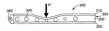
도 3a, 3b, 3c 및 3d는 전기적 접촉이 하나 이상의 단일 입자를 통한 물리적 접촉에 의해 달성되는 본 발명의 힘 감지 막의 사용례를 도시한다. 힘 감지 막(300)은 제1 전도체(310), 제2 전도체(320), 전도체들 사이에 배치된 엘라스토머 층(350)에 전도성 입자(340)를 포함하는 복합 재료(330), 및 힘 감지 막(360)을 가로질러 동적 전기 응답을 측정하는 수단을 구비한다. 도 3a에 도시한 바와 같이, 전도체들 사이에 압력을 인가하지 않을 때 전도체들(310 및 320)은 엘라스토머 층(350)에 의해 전기적으로 분리된 채로 유지된다. 도 3b에 도시한 바와 같이, 충분한 압력(P)을 제1 전도체(310)에 인가할 때, 전도체들(310 및 320) 사이에는 단일의 입자 접촉을 통해 전기적 접촉이 이루어질 수 있다. 단일 입자의 접촉은 하나 이상의 단일 전도성 입자들이 개별적으로 제1 전도체와 제2 전도체 모두와 접촉하는 경우에 제1 전도체와 제2 전도체 사이의 전기적 접촉이다. 도 3c에 도시한 바와 같이, 더 높은 압력(P')이 제1 전도체(310)에 인가될 때, 엘라스토머 층(350)은 추가로 압축되어 더 많은 단일 입자의 접촉이 이루어질 수 있다. 도 3d에 도시한 바와 같이, 모든 압력이 제거될 경우에, 엘라스토머 층(350)은 거의 그 본래의 치수로 복귀하며, 전기적 접촉은 이루어지지 않는다.3A, 3B, 3C and 3D illustrate examples of use of the force sensing membrane of the present invention in which electrical contact is achieved by physical contact through one or more single particles. The
전도성 입자는 모든 입자들이 크기 (또는 모양)가 동일하지 않도록 크기 분포를 가질 수 있다. 이러한 상황에서는, 전도성 입자들이 더 클수록 더 적은 인접 입자들 이전에 또는 그들 입자들을 배제하고 전기적 접촉을 이룰 수 있다. 이것이 발생하는지 여부 및 그 정도는 입자들의 크기 및 모양 분포, 입자 응집체의 존재 및 부재, 입자들의 적재 밀도 및 공간적 분포, 이동성 전도체 (또는 이동성 전도체/기재 조합체)가 구부러지고 국부적 변형을 따르는 능력, 입자들의 변형성, 입자들이 매립되는 엘라스토머 물질의 변형성 등에 따라 좌우된다. 제1 전도체와 제2 전도체 사이에 충분한 압력이 인가될 때는 단위당 바람직한 수의 단일 입자 전기 접촉이 이루어질 수 있도록 이들 및 기타 성질을 조정할 수 있다. 제1 전도체와 제2 전도체 사이에 인가된 상이한 양의 힘/압력에 대한 하나의 주어진 양의 압력에서 단위당 바람직한 수의 단일 입자 전기 접촉이 이루어지도록 성질들을 조정할 수도 있다.The conductive particles can have a size distribution such that all particles are not the same size (or shape). In such a situation, the larger the conductive particles can be in electrical contact before or without fewer adjacent particles. Whether this occurs and to what extent is the size and shape distribution of the particles, the presence and absence of particle aggregates, the loading density and spatial distribution of the particles, the ability of the mobile conductor (or mobile conductor / substrate combination) to bend and follow local deformation, the particles Deformability of the particles, the deformation of the elastomeric material in which the particles are embedded, and the like. When sufficient pressure is applied between the first conductor and the second conductor, these and other properties can be adjusted to allow for the desired number of single particle electrical contacts per unit. The properties may be adjusted such that a desired number of single particle electrical contacts are made per unit at one given amount of pressure for different amounts of force / pressure applied between the first and second conductors.
일부 실시 형태에서는 입자 크기 분포가 상대적으로 협소한 것이 바람직할 수 있고, 어떤 상황에서는 모든 입자들이 실질적으로 동일한 크기인 것이 바람직할 수 있다. 일부 실시 형태에서는 입자 크기의 두 가지 양식의 분포를 가지는 것이 바람직할 수 있다. 예컨대, 두 가지 상이한 유형의 입자들, 더 큰 입자들 및 더 작은 입자들이 복합 재료에 분산되게 하는 것이 바람직할 수 있다.In some embodiments, it may be desirable for the particle size distribution to be relatively narrow, and in some circumstances it may be desirable for all particles to be substantially the same size. In some embodiments, it may be desirable to have two forms of distribution of particle size. For example, it may be desirable to have two different types of particles, larger particles and smaller particles dispersed in the composite material.
도 4는 본 발명의 힘 감지 막의 또 다른 실시 형태를 도시한 것이다. 힘 감지 막(400)은 제1 전도체(410), 제2 전도체(420)에 배치된 엘라스토머 층(450)에 전도성 입자(440)를 포함하는 복합 재료(430), 및 힘 감지 막(460)을 가로질러 동적 전기 응답을 측정하는 수단을 구비한다. 스페이서(470)은 복합 재료(430)와 제1 전도체(410) 사이에 갭(480, 예컨대, 공기 갭)을 생성시킨다. 복합 재료와 전도체 사이에 공기의 갭을 부가하면 힘 감지 막의 민감도가 변화되며, 따라서 센서를 특정 용도로 조정하는 데에 유용할 수 있다. 한편, 상기 갭은 비전도성 충전재로 충전될 수 있다. 갭을 충전하면, 충전재가 제공하는 보호로 인해 분쇄 및 박편화되기 쉬운 전도체 (예컨대, 투명 전도성 층)를 가지는 힘 감지 막에서 증가된 내구성 같은 장점을 얻을 수 있다.Figure 4 shows another embodiment of the force sensing membrane of the present invention. The
본 발명의 힘 감지 막은 엘라스토머 층을 엠보싱 처리하여 (예컨대, 미세 복제 표면(microreplicated surface)을 제공하기 위해) 특정 용도에 맞출 수도 있다. 엘라스토머 층을 엠보싱 처리하면 공기가 막의 내외로 자유로이 이동할 수 있고, 따라서 막의 활성화 힘을 낮출 수 있다. 엠보싱은 단락을 방지할 수도 있다. 한편, 미소구(microsphere)(예컨대, 악조 노벨에서 시판되는 상표명 엑스판셀 미소구)를 엘라스토머 층에 분산시킬 수도 있다.The force sensing film of the present invention may be embossed with an elastomeric layer (eg, to provide a microreplicated surface) to suit a particular application. Embossing the elastomer layer allows air to move freely in and out of the membrane, thus lowering the activation force of the membrane. Embossing may prevent short circuits. On the other hand, microspheres (e.g., the trade name Xpancel microspheres available from Akzo Novell) may be dispersed in the elastomer layer.
도 5a 및 5b는 두 개의 층 구조를 가지는 본 발명에 따른 힘 감지 막의 실시 형태를 도시한 것이다. 도 5a에서, 힘 감지 막(500)은 제1 전도체(510) 상에 배치된 엘라스토머 층(590), 및 제2 전도체(520) 상에 배치된 절연 재료(550)에 전도성 입자(540)를 포함하는 복합층(530)을 구비한다. 힘 감지 막을 가로질러 동적 전기 응답을 측정하는 수단 (도시하지 않음)은 힘 감지 막에 전기적으로 연결될 수 있다. 복합층의 두께는 전도성 입자의 평균 크기 미만인 것이 바람직하다. 제1 전도체 상에 배치된 엘라스토머 층은 복합층이 너무 얇은 것으로 인해 생기는 전기적 단락을 (예기치 않은 전극-입자-전극 전기적 접촉으로부터) 방지할 수 있다.5a and 5b show an embodiment of a force sensing membrane according to the present invention having a two layer structure. In FIG. 5A, the
도 5b에서, 전도성 입자(540)는 그들 중 적어도 일부가 제2 전도체(520)와 항상 접촉 상태가 되도록 (예컨대, 롤 닙을 통과시켜서) 압축된다. 입자들이 절단되고 복합층의 두께가 조절되어 평균 입자 크기 미만으로 될 때, 활성화 힘 (즉, 제1 전도체와 제2 전도체를 전기적으로 연결하는 데 필요한 힘)은 엘라스토머 층의 두께와 성질에 의해 조절된다. 절연 재료의 성질 및 복합층의 전도성은 활성화 힘에 상대적으로 적은 효과를 가진다. 따라서, 힘 감지 막은 특정 활성화 힘을 가지도록 설계될 수 있다.In FIG. 5B, the
절연 재료는 임의의 절연성이고 필름을 형성하며 경화 가능한 재료일 수 있다. 절연 재료는 엘라스토머 또는 비엘라스토머 물질일 수 있다. 절연 재료는 예컨대, 우레탄, 에폭시, 아크릴레이트, 폴리에스테르, 폴리올레핀, 폴리아미드 등 및 이들의 혼합물을 포함할 수 있다. 절연 재료로는 압력 해제 시에 거의 그 본래의 치수로 복귀할 수 있는 엘라스토머 물질이 바람직하다. 절연 재료는 약 0℃ 내지 약 100℃에서, 가장 바람직하게는 약 0℃ 내지 약 60℃에서 거의 일정한 G' (경화 가능한 재료라면 그 완전히 경화된 상태로)을 가지는 엘라스토머 물질을 포함하는 것이 더 바람직하다. 엘라스토머 물질은 약 1 x 10³ Pa/㎠ 내지 약 9 x 10⁵ Pa/㎠의 G' 및 23℃, 1 Hz에서 약 0.01 내지 약 0.60의 손실 탄젠트 (tan Δ)를 가지는 것이 바람직하다. 엘라스토머 물질은 자가-치유성인 것도 바람직하다. The insulating material may be any insulating, film forming and curable material. The insulating material may be an elastomeric or nonelastomeric material. Insulating materials may include, for example, urethanes, epoxies, acrylates, polyesters, polyolefins, polyamides, and the like and mixtures thereof. Preferred insulating materials are elastomeric materials that can return to their original dimensions upon release of pressure. It is more preferred that the insulating material comprises an elastomeric material having a substantially constant G '(in the fully cured state if curable material) at about 0 ° C to about 100 ° C, most preferably at about 0 ° C to about 60 ° C. Do. The elastomeric material preferably has a G 'of about 1 × 10 3 Pa / cm 2 to about 9 × 10 5 Pa / cm 2 and a loss tangent (tan Δ) of about 0.01 to about 0.60 at 23 ° C., 1 Hz. It is also preferred that the elastomeric material is self-healing.
본 발명의 2-층 힘 감지 막에서, 엘라스토머 층 또는 절연 재료 층, 또는 그 둘다는 엠보싱 처리될 수 있다.In the two-layer force sensing film of the present invention, an elastomeric layer or insulating material layer, or both, can be embossed.
본 발명의 힘 감지 막은 전도체들 중의 하나 또는 둘다에 오버레이(overlay) 층 (예컨대, 플라스틱 필름 또는 발포체 층)을 포함할 수도 있다. 통상, 오버레이 층은 힘 감지 막의 응답에 영향을 끼치지 않도록 약 5 ㎜ 미만 (바람직하게는 약 2㎜ 미만)의 두께를 가진다. 오버레이 층은 의료 분야에서 (예컨대, 압력을 모니터하여 욕창, 당뇨성 족부 궤양 또는 깁스 하의 과다 압력을 방지하기 위해) 힘 감지 막을 사용할 때 특히 유용하다. 의료용 압력 감지 용도에 유용한 오버레이 층의 예로는 신발용 발포 깔창, 침대 시트, 붕대 및 양말을 들 수 있다.The force sensing membrane of the present invention may include an overlay layer (eg, plastic film or foam layer) on one or both of the conductors. Typically, the overlay layer has a thickness of less than about 5 mm (preferably less than about 2 mm) so as not to affect the response of the force sensing film. Overlay layers are particularly useful in the medical field when using force sensing membranes (eg, to monitor pressure to prevent pressure sores under pressure from bedsores, diabetic foot ulcers or casts). Examples of overlay layers useful for medical pressure sensing applications include shoe foam insoles, bed sheets, bandages, and socks.
본 발명의 힘 감지 막은 적합한 재료에 캡슐화되어 물/습기 내성을 제공할 수도 있다.The force sensing membrane of the present invention may be encapsulated in a suitable material to provide water / moisture resistance.
본 발명의 힘 감지 막은 다수의 응용 분야에 유용하다. 예컨대, 본 발명의 힘 감지 막은 깁스 하의 과다 압력을 변화시키거나 또는 욕창 및 당뇨성 족부 궤양의 방지용으로 압력을 모니터하는 것과 같은 헬스케어 분야에 유용할 수 있다. 본 발명의 힘 감지 막이 환자의 피부와 접촉하거나 매우 가까이 근접하는 경우, 이들 막은 수증기를 투과하여 수증기가 피부로부터 증발되게 한다.The force sensing membrane of the present invention is useful for many applications. For example, the force sensing membrane of the present invention may be useful in the field of healthcare, such as changing the pressure under the cast or monitoring pressure for the prevention of pressure sores and diabetic foot ulcers. When the force sensitive membranes of the present invention come into contact with or in close proximity to the skin of a patient, these membranes penetrate the water vapor causing vapor to evaporate from the skin.
당뇨병이 있는 다수의 개인은 질병이 진행함에 따라 더 하단의 다리에서 불량한 감각을 경험한다. 통상, 이들 개인은 과다 압력 또는 피부 궤양이 발의 피부 상에 나타나고 있는지 여부를 측정하기 위해 시각적 관찰만을 사용한다. 그러한 궤양은 통상 앉았다 섰다를 오랜 시간 반복함으로써 발의 특정 지점에 가해진 압력 및/또는 전단력의 결과이다. 본 발명의 힘 감지 막은 발의 압력 평가를 허용한다. 예컨대, 본 발명의 힘 감지 막은 양말, 붕대 또는 깔창 내로 도입되어 (포켓에 기워지거나, 뜨개질되거나, 접착 또는 열적 방식으로 결합되거나, 후크 및 루프 장치에 의해 부착되거나, 삽입되거나 또는 임의의 적합한 수단에 의해 도입되어) 당해 발 영역 상의 압력을 측정할 수 있다. 상기 막은 데이터 이력용 마이크로프로세서 또는 분리된 로직에 전기적으로 연결될 수 있다. 힘 감지 막은 지정된 압력 역치가 초과될 때 청각, 시각 또는 감각 (예컨대, 진동) 응답을 제공하기 위해 신호 처리 유닛에 전기적으로 연결될 수도 있다.Many individuals with diabetes experience poor sensations in the lower legs as the disease progresses. Typically, these individuals use only visual observation to determine whether excessive pressure or skin ulcers are present on the skin of the foot. Such ulcers are usually the result of pressure and / or shear forces exerted on a particular point of the foot by repeated sitting and standing for a long time. The force sensitive membrane of the present invention allows evaluating foot pressure. For example, the force sensing membrane of the present invention may be introduced into a sock, bandage or insole (either inclined, knitted, glued or thermally coupled to a pocket, attached by a hook and loop device, inserted or in any suitable means). Can be used to measure the pressure on the foot area. The membrane may be electrically connected to a microprocessor for data history or separate logic. The force sensing membrane may be electrically connected to the signal processing unit to provide an audible, visual or sensory (eg, vibrational) response when the specified pressure threshold is exceeded.
본 발명의 다수의 힘 감지 막을 포함하는 배열은 헬스케어 분야에도 유용할 수 있다. 예컨대, 힘 감지 막의 배열을 침대의 다양한 위치에서 정렬하여 욕창 예방용 압력을 모니터할 수 있다. 힘 감지 배열은 균일하게 또는 비균일하게 이격될 수 있다.Arrangements comprising multiple force sensing membranes of the present invention may also be useful in the healthcare field. For example, an array of force sensing membranes can be aligned at various locations in the bed to monitor pressure for preventing bedsores. The force sensing arrangements can be spaced uniformly or nonuniformly.
본 발명의 힘 감지 막은 또한 예컨대, 자동차 분야 (예컨대, 좌석 센서 또는 에어백 전개용), 소비자 분야 (예컨대, 하중/중량 센서로서 또는 선반의 물품의 존재 또는 그 부족을 감지하는 "스마트 시스템"에서), 제조 분야 (예컨대, 닙 롤 압력을 모니터하는 용도), 스포츠 분야 (예컨대, 속도, 힘 또는 충격을 모니터하거나, 또는 클럽이나 라켓 상의 그립 센서로서) 등에 유용하다.The force sensing membrane of the present invention is also useful in, for example, the automotive sector (eg for seat sensors or airbag deployment), the consumer sector (eg as a load / weight sensor or in a "smart system" that detects the presence or lack of an item on the shelf). , The field of manufacture (eg, for monitoring nip roll pressure), the field of sports (eg, monitoring speed, force or impact, or as a grip sensor on a club or racket) and the like.
본 발명의 목적 및 장점은 하기 실시예들에 의해 추가로 예시되며, 이들 실시예에 언급되는 특정 재료 및 그 양은 기타 조건 및 상세와 함께 본 발명을 부당하게 제한하는 것으로 해석되어서는 아니된다.The objects and advantages of the present invention are further illustrated by the following examples, and the specific materials and amounts thereof referred to in these examples should not be construed as unduly limiting the present invention with other conditions and details.
재료material
실시예들에 사용된 재료는 하기 표에 도시되어 있다. 재료의 조성은 phr (고무의 100부당 부)로 표현한다. UC 실리콘은 크롬프턴사 (코네티컷주 그린위치 소재)의 Y-7942로서 시판되는 비닐 개질된 폴리 디메틸 실록산이며; PT 촉매는 1 phr의 UC 실리콘에 분산되어 있는 알드리치 카나다 (카나다 온타리오주 오크빌 소재)에서 시판되는 백금 미세 분말의 분산액이고; DC1107은 다우 코닝 (미시건주 미드랜드)에서 시판되는 가교제이며; DM은 피셔 사이언티픽 (카나다 온타리오주 오타와)에서 시판되는 디메틸 말레에이트이고; 실리카는 캐벗 코퍼레이션 (일리노이주 투손 소재)에서 M3 Cab-o-sil로서 시판되는 발연 실리카(fumed silica)이다.The materials used in the examples are shown in the table below. The composition of the material is expressed in phr (parts per 100 parts of rubber). UC silicone is vinyl modified poly dimethyl siloxane, commercially available as Y-7942 from Cromtonton, Greenwich, Connecticut; The PT catalyst is a dispersion of platinum fine powders available from Aldrich Canada (Oakville, Ontario, Canada) dispersed in 1 phr of UC silicon; DC1107 is a crosslinker commercially available from Dow Corning (Midland, Michigan); DM is dimethyl maleate commercially available from Fisher Scientific (Ottawa, Ontario, Canada); Silica is fumed silica sold as M3 Cab-o-sil at Cabot Corporation (Tucson, Ill.).
G165730N은 상표명 크레이튼 G1657 (텍사스주 휴스톤 소재의 크레이튼 폴리머스에서 시판됨) 및 30 phr의 나이플렉스 22b 처리 오일 (텍사스주 휴스톤 소재의 나이나스 USA 인크에서 시판됨)의 혼합물이었다.G165730N was a mixture of trade name Creighton G1657 (available from Creighton Polymers, Houston, Texas) and 30 phr of Neplex 22b treated oil (available from Nana's USA Inc., Houston, Texas).
시험 유닛Test unit
센서에 가해진 정상 힘을 측정하는 하중 셀 (코네티컷주 하트포드 소재의 오메가 엔지니어링 인크에서 시판되는 모델 LCFD-1kg)로 구성되는 힘 장치로 불리는 장치를 사용하여 센서를 평가하였다. 평가할 센서는 하중 셀 상에 수평으로 배치하 고 테이프로 고정하였다. 약 275 kPa에서 압축된 공기로 컴퓨터 제어 하에 두 밸브 (오하이오주 신시내티 소재의 클리파드 인스트루먼트 래보러토리에서 시판되는 모델 EC-2-12)에 연결된 공기압으로 작동되는 실린더 (코네티컷주 노워크 소재의 에어팟 코포레이션에서 시판되는 모델 E9X 0.5N)를 상기 하중 셀 위로 직접 배치하였다. 밸브를 순서대로 개봉 및 폐쇄함으로써, 실린더는 하중 셀 상에 배치된 센서 상의 힘을 증가시키기 위해 예정된 일정한 단계로 하단으로 이동시켰다. 하중 셀은 인가된 힘을 나타내는 디스플레이 장치 (코네티컷주 하트포드 소재의 오메가 엔지니어링 인크에서 시판되는 모델 DP41-S-A)에 연결되었다. 힘의 예정된 한계에 도달하면, 통기 밸브를 사용하여 공기를 시스템으로부터 통기시켜 센서 상의 힘을 감소시켰다.The sensor was evaluated using a device called a force device consisting of a load cell (model LCFD-1 kg, available from Omega Engineering Inc., Hartford, Connecticut) measuring the normal force applied to the sensor. The sensor to be evaluated was placed horizontally on the load cell and fixed with tape. Pneumatically operated cylinders (Norwalk, CT) connected to two valves (Model EC-2-12, available from the Clifford Instrument Laboratories, Cincinnati, Ohio) under computer control with compressed air at approximately 275 kPa. A commercially available model E9X 0.5N from Pod Corp. was placed directly onto the load cell. By opening and closing the valves in sequence, the cylinder was moved to the bottom in a predetermined predetermined step to increase the force on the sensor disposed on the load cell. The load cell was connected to a display device representing the applied force (model DP41-S-A, commercially available from Omega Engineering Inc., Hartford, Connecticut). Once the predetermined limit of force was reached, a vent valve was used to vent air from the system to reduce the force on the sensor.
센서의 전도체들은 멀티미터에 연결하여 센서의 전기 응답을 기록하였다. 센서의 저항은 디지털 멀티미터 (오하이오주 클래브랜드 소재의 키슬리 인크에서 시판되는 키슬리 모델 197A 마이크로볼트 DMM)를 사용하여 측정하였다. 하중 셀로부터 판독되는 인가된 힘 및 멀티미터로부터 판독되는 센서의 전기 응답을 PC에 기초한 테이터 획득 시스템으로 포착하였다. 부가된 힘은 0.1 내지 10 뉴턴의 범위였으며, 힘의 부가는 약 0.028 뉴턴/s (1.67 뉴턴/분)의 속도로 실시하였다.The conductors of the sensor were connected to the multimeter and recorded the electrical response of the sensor. The resistance of the sensor was measured using a digital multimeter (Kisley Model 197A microvolt DMM, available from Keithley Inc., Cleveland, Ohio). The applied force read from the load cell and the electrical response of the sensor read from the multimeter were captured with a PC based data acquisition system. The added force ranged from 0.1 to 10 Newtons, and the addition of force was conducted at a rate of about 0.028 Newtons / s (1.67 Newtons / minute).
n-값의 설명Description of the n-value
힘 센서를 가로질러 저항을 측정할 때, 저항 대 힘의 관계를 로그-로그 도표로 작성할 수 있다. 특정 범위에서, 힘의 법칙 관계는 저항 = A/Fn의 식으로 제시될 수 있는데, 여기서, A는 상수이고, F는 힘이며, n ("n-값")은 로그-로그 도표 상에서 최적 라인의 기울기 (선형 회귀에 의해 측정됨)이다. n-값은 센서의 민감도를 나타낸다. n-값이 높을수록 가해진 힘에 주어진 변화에 대해 센서의 저항의 변화가 더 커진다. n-값이 더 낮다는 것은 가해진 힘에서의 동일한 변화에 대해 저항의 변화가 더 작다는 것을 뜻한다.When measuring resistance across a force sensor, a log-log plot of the resistance versus force relationship can be created. In a particular range, the law of force relation can be given by the formula resistance = A / F n , where A is a constant, F is a force, and n ("n-value") is optimal on the log-log plot Slope of the line (measured by linear regression). The n-value represents the sensitivity of the sensor. The higher the n-value, the larger the change in the resistance of the sensor for a given change in force applied. Lower n-values mean smaller changes in resistance for the same change in applied force.
RR 22 의 설명Description of
전술한 바와 같이, 저항 대 힘의 관계는 로그-로그 도표로 작성할 수 있으며, 최적 라인을 측정할 수 있다. 당해 분야에 알려진 바와 같이, 선형 회귀의 적합도 (또는 적합도의 척도)는 R2 값에 의해 나타낼 수 있다. R2는 0.0 내지 1.0 사이의 분율이다. R2가 1.0에 가까울수록 적합도가 더 양호해진다. R2가 1.0일 경우, 모든 작성된 점들은 산포 없는 직선에 정확히 존재한다.As mentioned above, the relationship of resistance to force can be plotted in log-log plots and the optimal line can be measured. As known in the art, the goodness of fit (or measure of goodness of fit) of a linear regression can be represented by an R 2 value. R 2 is a fraction between 0.0 and 1.0. The closer R 2 is to 1.0, the better the fitness. If R 2 is 1.0, all created points are exactly on a straight line without scatter.
실시예Example 1 One
3M 컴퍼니 (미네소타주 세인트 폴 소재)에서 SD220으로 시판되는 인듐 주석 산화물 (ITO) 코팅된 유리 섬유를 734-실리콘 고무 (미시건주 미드랜드 소재의 다우 코닝)의 비경화된 나이프 코팅 층 (약 25 미크론의 두께) 위로 분배하였다. 미국 특허출원 공보 제03/0129302호 (Chambers 등)에 기재된 입자 분배기를 사용하여 입자를 분배하였다. 실리콘 고무를 실온에서 밤새 경화한 후에, 입자-매립된 실리콘 고무의 작은 조각 (약 20 ㎜ x 20 ㎜)을 절단하여 구리 호일 테이프 (미네소타주 세인트 폴 소재의 3M 컴퍼니의 3M 1190) 상에 옮기고 입자-매립된 실리콘의 가 장자리 주위로 테이프를 바름으로써 3M 스카치 테이프를 사용하여 고정시켰다. 또 다른 구리 호일 테이프를 이것의 정상부에 배치하여 두 개의 구리 호일이 서로 접촉되지 않게 하였다. 두 개의 구리 호일을 스카치 테이프로 서로로부터 전기적으로 분리시켰다.Indium tin oxide (ITO) coated glass fibers, commercially available as SD220 from 3M Company, St. Paul, Minn, were coated with an uncured knife coating layer of about 734-silicone rubber (Dow Corning, Midland, MI) Thickness). Particles were distributed using a particle dispenser described in US Patent Application Publication No. 03/0129302 (Chambers et al.). After the silicone rubber was cured overnight at room temperature, a small piece of particle-embedded silicone rubber (about 20 mm x 20 mm) was cut and transferred onto copper foil tape (3M 1190, 3M Company, St. Paul, Minn.) Fixed using 3M Scotch tape by applying tape around the edges of the embedded silicon. Another copper foil tape was placed on top of it so that the two copper foils did not contact each other. The two copper foils were electrically separated from each other with scotch tape.
생성되는 센서는 전술한 힘 장치 시험 유닛을 사용하여 시험하였다. 로그-로그 도표에 작성된 시험 데이터는 도 6에 도시하였다. 최적 라인의 n-값은 1.02이고, R2는 0.992이다.The resulting sensor was tested using the force device test unit described above. Test data written in the log-log chart is shown in FIG. 6. The n-value of the optimal line is 1.02 and R 2 is 0.992.
실시예Example 2 2
실시예 1에 기재한 센서는 다음과 같이 적재 및 탈적재 사이클을 반복함으로써 그 내구성에 대해 시험하였다.The sensor described in Example 1 was tested for its durability by repeating the loading and unloading cycle as follows.
라이프 사이클 테스트 시스템 (일리노이주 엘긴 소재의 트리코르 시스템스 인크의 모델 933A)을 사용하여 내구성의 관점에서 센서를 시험하였다. 테스트 시스템은 공기압으로 조절되는 실린더를 가지는데, 이 실린더는 업/다운 사이클 수를 계수하면서 센서를 선택된 속도로 가압하였다. 센서를 가로질러 연결된 멀티미터는 그것을 가로질러 나타나는 전압을 측정하였다. 센서는 1000 사이클에 대해 시험하였고, 각 사이클에 대해 대략 동일한 전압 대 힘의 곡선을 산출하는 것으로 보였다.The sensors were tested in terms of durability using a life cycle test system (Model 933A from Tricor Systems Inc., Elgin, Ill.). The test system has a cylinder that is controlled by air pressure, which presses the sensor at the selected speed while counting the number of up / down cycles. The multimeter connected across the sensor measured the voltage across it. The sensor was tested for 1000 cycles and appeared to yield approximately the same voltage versus force curve for each cycle.
실시예Example 3 3
실시예 1에 기재한 센서를 LED (발광 다이오드) 막대 그래프 디스플레이 회 로에 연결하였다. 센서 상에 손가락으로 눌러서 힘을 센서에 가하면, 가해진 힘에 응답하여 디스플레이는 LED의 분절을 밝혔다.The sensor described in Example 1 was connected to an LED (light emitting diode) bar graph display circuit. When a finger was pressed on the sensor to apply a force to the sensor, the display revealed an LED segment in response to the applied force.
실시예Example 4 4
센서 상에 상이한 오버레이 재료를 배치한 후에 힘 장치 시험 유닛을 사용하여, 실시예 1에 기재한 것과 거의 동일한 센서의 특성을 상기와 같이 측정하였다. 오버레이 재료는 센서의 정상부에 간단히 배치하였다. 오버레이는 다음 재료를 포함하였다:After placing different overlay materials on the sensors, the force device test unit was used to measure the properties of the sensor which were nearly identical to those described in Example 1 as above. The overlay material was simply placed on top of the sensor. The overlay included the following materials:
1. Melinex TM 폴리에스테르 필름 (버지니아주 호프웰 소재의 듀퐁); 및1. Melinex ™ polyester film (Dupont, Hopewell, VA); And
2. 140 mil 두께의 EquateTM 발포 쿠션 깔창 (카나다 온타리오 다운스뷰 소재의 내셔널 홈 프로덕츠 리미티드)2. 140 mil Equate TM foam cushion insole having a thickness (Ontario Canada Downs view National Home Products Limited of material)
센서 특성은 표 1 (폴리에스테르 필름) 및 표 2 (발포 깔창)에 나타낸 오버레이어의 도포 시에 기본적으로 변화하지 않았다. n-값은 센서의 정상부에 상이한 오버레이어를 배치하면 센서의 감도를 현저하게 변화시키지 않음을 나타낸다.Sensor properties did not change fundamentally upon application of the overlayer shown in Table 1 (polyester film) and Table 2 (foamed insole). The n-value indicates that placing different overlayers on top of the sensor does not significantly change the sensitivity of the sensor.
실시예Example 5 5
전도체와 복합 재료층 사이의 공기 갭의 영향을 분석하기 위하여, 실시예 1에 기재한 것과 거의 동일한 방식으로 3M 810 테이프 (미네소타주 세인트 폴)를 사용하여 센서의 실리콘 고무 층과 정상부 구리 호일 테이프 사이에 공간을 생성시켰다. 후술하는 공기 갭 두께를 가진 힘 장치 시험 유닛을 사용하여 상기 센서를 시험하였다. 그 결과 (표 3)는 공기 갭이 증가함에 따라 센서의 감도는 증가된 n-값으로 나타나는 바와 같이 증가되었음을 나타낸다.To analyze the effect of the air gap between the conductor and the composite material layer, the 3M 810 tape (St. Paul, Minn.) Was used between the silicon rubber layer of the sensor and the top copper foil tape in much the same way as described in Example 1. To create space. The sensor was tested using a force device test unit with an air gap thickness described below. The results (Table 3) indicate that as the air gap increased, the sensitivity of the sensor increased as indicated by the increased n-value.
실시예Example 6 6
아래에 제시하는 엘라스토머와 인듐 주석 산화물 (ITO) 코팅된 유리 비드를 섬유 대신에 사용하는 것을 제외하고는 실시예 1에 기재한 것과 거의 동일하게 센서를 제조하였다. 3M 컴퍼니 (미네소타주 세인트 폴 소재)에서 SD110으로 시판되는 인듐 주석 산화물 (ITO) 코팅된 유리 비드를 아래에 나타낸 약 1 mil (25 미크론) 이하의 두께인 비경화된 나이프 코팅된 엘라스토머 층 위로 분배하였다. 힘 장치 시험 유닛을 사용하여 센서들을 시험하였다. 저항 1 kOhm을 나타내는 데 필요한 힘으로 정의되는 센서의 활성화 힘 (Fi)도 기록하였다.The sensor was prepared in much the same manner as described in Example 1 except for using the elastomer and indium tin oxide (ITO) coated glass beads shown below in place of the fibers. Indium tin oxide (ITO) coated glass beads sold as SD110 in 3M Company, St. Paul, Minn., Were dispensed onto a layer of uncured knife coated elastomer having a thickness of about 1 mil (25 microns) or less shown below. . The sensors were tested using a force device test unit. The activation force (F i ) of the sensor, also defined as the force required to represent 1 kOhm of resistance, was also recorded.
실시예Example 7 7
당해 엘라스토머 (표 5에 "기저부" 엘라스토머로 나타냄)를 ITO 코팅된 폴리에스테르의 전도성 층 상에 나이프 코팅하여 37.5 미크론 (1.5 mil)의 두께를 얻었다. ITO 코팅된 유리 비드는 대략 1.5 g/ft2 밀도에서 엘라스토머 층 상에 분배하였다. 입자들은 두 고무 롤 사이에 코팅된 엘라스토머를 물림으로써 엘라스토머 층 내로 매립시켰다. 이 코팅된 엘라스토머는 오븐에서 5분 동안 120℃에서 공기 중에서 경화하였다. ITO 코팅된 폴리에스테르의 별개의 전도성 층 상에, 엘라스토머 (표 5에 "정상부" 엘라스토머로 나타냄)를 두께 12.5 미크론 (0.5 mil)으로 나이프 코팅하고, 엘라스토머를 오븐에서 120℃의 공기 중에서 5분 동안 경화하였다. 엘라스토머들이 서로 마주보도록 두 층을 결합시키고, 포장용 페이프 (미네소타주 세인트 폴 소재의 3M 컴퍼니의 3M 3710 테이프)로 테이핑하였다. 구리 전기 호일 테이프 (미네소타주 세인트 폴 소재의 3M 컴퍼니의 3M 1190)를 사용하여 두 전도성 층을 전기적으로 연결시키고, 센서는 힘 장치 시험 유닛을 사용하여 시험하였다. 그 결과는 표 5에 제시한다.The elastomer (represented as "base" elastomer in Table 5) was knife coated onto a conductive layer of ITO coated polyester to obtain a thickness of 37.5 microns (1.5 mil). ITO coated glass beads were dispensed onto the elastomer layer at a density of approximately 1.5 g / ft 2 . The particles were embedded into the elastomer layer by biting the coated elastomer between two rubber rolls. This coated elastomer was cured in air at 120 ° C. for 5 minutes in an oven. On a separate conductive layer of ITO coated polyester, an elastomer (represented as "top" elastomer in Table 5) is knife coated to a thickness of 12.5 microns (0.5 mil), and the elastomer is in the oven for 5 minutes in air at 120 ° C. Cured. The two layers were joined so that the elastomers faced each other and taped with packaging paper (3M 3710 tape from 3M Company, St. Paul, Minn.). Two conductive layers were electrically connected using copper electrical foil tape (3M 1190, 3M Company, St. Paul, Minn.), And the sensor was tested using a force device test unit. The results are shown in Table 5.
1 kOhm의 저항을 나타내는 데 필요한 힘으로 정의되는 각 센서의 활성화 힘 (Fi)과 함께 정상부 엘라스토머 층의 G' 및 tan (Δ)와 n-값은 하기 표 5에 제시한다. 엘라스토머는 탄성률이 높을수록 높은 활성화 힘 및 보다 높은 n-값과 힘에 대한 보다 높은 감도를 나타냈다.The G 'and tan (Δ) and n-values of the top elastomer layer along with the activation force (F i ) of each sensor, defined as the force required to represent a resistance of 1 kOhm, are presented in Table 5 below. Elastomers exhibited higher activation forces and higher sensitivity to n-values and forces at higher elastic modulus.
본 발명에 대한 다양한 개조예 및 변형예는 본 발명의 범위와 사상으로부터 벗어나지 않으면서 당업자에게는 명확해질 것이다. 본 발명은 본 명세서에 제시한 예시적 실시 형태 및 실시예에 의해 부당하게 제한되어서는 아니되며, 그러한 실시예 및 실시 형태는 이하에 제시하는 특허 청구의 범위에 의해서만 제한될 본 발명의 범위와 관련하여서만 예시로서 제시된다는 점을 이해하여야 한다.Various modifications and variations of the present invention will become apparent to those skilled in the art without departing from the scope and spirit of the invention. The invention is not to be unduly limited by the exemplary embodiments and examples presented herein, which examples and embodiments relate to the scope of the invention which will be limited only by the claims set out below. It should be understood that the examples are given only as examples.
Claims (46)
Applications Claiming Priority (2)
| Application Number | Priority Date | Filing Date | Title |
|---|---|---|---|
| US11/020,289 | 2004-12-23 | ||
| US11/020,289 US7260999B2 (en) | 2004-12-23 | 2004-12-23 | Force sensing membrane |
Publications (1)
| Publication Number | Publication Date |
|---|---|
| KR20070090035A true KR20070090035A (en) | 2007-09-04 |
Family
ID=36104499
Family Applications (1)
| Application Number | Title | Priority Date | Filing Date |
|---|---|---|---|
| KR1020077016976A KR20070090035A (en) | 2004-12-23 | 2005-12-19 | Force sensing membrane |
Country Status (11)
| Country | Link |
|---|---|
| US (1) | US7260999B2 (en) |
| EP (1) | EP1828732A1 (en) |
| JP (1) | JP5399634B2 (en) |
| KR (1) | KR20070090035A (en) |
| CN (1) | CN100541153C (en) |
| AU (1) | AU2005322227A1 (en) |
| BR (1) | BRPI0518566A2 (en) |
| CA (1) | CA2590870A1 (en) |
| MX (1) | MX2007007552A (en) |
| TW (1) | TW200634291A (en) |
| WO (1) | WO2006071690A1 (en) |
Cited By (1)
| Publication number | Priority date | Publication date | Assignee | Title |
|---|---|---|---|---|
| KR20150034332A (en) * | 2013-09-26 | 2015-04-03 | 국민대학교산학협력단 | Method for sensitivity control of pressure sensor using layer-by-layer self assembley |
Families Citing this family (47)
| Publication number | Priority date | Publication date | Assignee | Title |
|---|---|---|---|---|
| US6955094B1 (en) * | 2003-07-18 | 2005-10-18 | Cleveland Medical Devices Inc. | Sensor for measuring shear forces |
| FR2872030B1 (en) * | 2004-06-24 | 2006-08-25 | Centre Nat Rech Scient Cnrse | ESCARTER PREVENTION DEVICE |
| US7468199B2 (en) * | 2004-12-23 | 2008-12-23 | 3M Innovative Properties Company | Adhesive membrane for force switches and sensors |
| US7509881B2 (en) * | 2005-07-29 | 2009-03-31 | 3M Innovative Properties Company | Interdigital force switches and sensors |
| CN100535648C (en) * | 2006-09-12 | 2009-09-02 | 吕志刚 | Damage detection information smart coat with subsidiary damage feature |
| JP5568206B2 (en) * | 2006-09-15 | 2014-08-06 | 東海ゴム工業株式会社 | Deformation sensor |
| WO2008052017A2 (en) | 2006-10-23 | 2008-05-02 | Patrick Antaki | Flexible fingerprint sensor |
| EP1916529B1 (en) * | 2006-10-25 | 2011-03-16 | Tokai Rubber Industries, Ltd. | Deformation sensor |
| US9027408B2 (en) | 2007-01-24 | 2015-05-12 | Swelling Solutions, Inc. | Elastomeric particle having an electrically conducting surface, a pressure sensor comprising said particles, a method for producing said sensor and a sensor system comprising said sensors |
| US9018030B2 (en) * | 2008-03-20 | 2015-04-28 | Symbol Technologies, Inc. | Transparent force sensor and method of fabrication |
| US20090237374A1 (en) * | 2008-03-20 | 2009-09-24 | Motorola, Inc. | Transparent pressure sensor and method for using |
| US9459734B2 (en) * | 2009-04-06 | 2016-10-04 | Synaptics Incorporated | Input device with deflectable electrode |
| US9383881B2 (en) * | 2009-06-03 | 2016-07-05 | Synaptics Incorporated | Input device and method with pressure-sensitive layer |
| US8988191B2 (en) * | 2009-08-27 | 2015-03-24 | Symbol Technologies, Inc. | Systems and methods for pressure-based authentication of an input on a touch screen |
| TWI407561B (en) * | 2009-11-10 | 2013-09-01 | Univ Nat Chiao Tung | Pressure detector and an array thereof |
| JP5501064B2 (en) | 2010-03-29 | 2014-05-21 | 富士フイルム株式会社 | Elastic material for pressure measurement and pressure measuring device |
| US20110273394A1 (en) * | 2010-05-10 | 2011-11-10 | Symbol Technologies, Inc. | Methods and apparatus for a transparent and flexible force-sensitive touch panel |
| US8963874B2 (en) | 2010-07-31 | 2015-02-24 | Symbol Technologies, Inc. | Touch screen rendering system and method of operation thereof |
| WO2012055029A1 (en) | 2010-10-29 | 2012-05-03 | Orpyx Medical Technologies Inc. | Peripheral sensory and supersensory replacement system |
| CN103091005B (en) * | 2011-11-07 | 2015-02-18 | 中国医药大学 | Pressure sensing component |
| JP5871129B2 (en) * | 2012-02-13 | 2016-03-01 | 日産自動車株式会社 | Cloth pressure sensor |
| JP6139678B2 (en) | 2012-07-19 | 2017-05-31 | スリーエム イノベイティブ プロパティズ カンパニー | Determination of elastic bandage elongation |
| JP2014126373A (en) * | 2012-12-25 | 2014-07-07 | China Medical Univ | Pressure detector |
| JP6420321B2 (en) | 2013-05-21 | 2018-11-07 | オーピクス・メディカル・テクノロジーズ・インコーポレイテッド | Pressure data acquisition assembly |
| EP3021801B1 (en) * | 2013-07-18 | 2017-10-25 | Coloplast A/S | Touch mapping |
| WO2015066337A1 (en) | 2013-10-31 | 2015-05-07 | University Of Florida Research Foundation, Inc. | Porous polymer membranes, methods of making, and methods of use |
| WO2016108996A1 (en) * | 2014-10-17 | 2016-07-07 | The University Of Florida Research Foundation, Inc. | Methods and structures for light regulating coatings |
| US9421087B1 (en) | 2015-04-27 | 2016-08-23 | International Business Machines Corporation | Artificial electronic skin |
| US10189967B2 (en) | 2015-05-08 | 2019-01-29 | University Of Florida Research Foundation, Inc. | Macroporous photonic crystal membrane, methods of making, and methods of use |
| TWI575232B (en) | 2015-06-12 | 2017-03-21 | 財團法人工業技術研究院 | Sensing device |
| CN108697374B (en) * | 2016-01-13 | 2021-09-17 | 丹麦专用绷带股份有限公司 | Apparatus and method for providing a measure of the circumference of a body part |
| DK3402401T3 (en) | 2016-01-13 | 2021-06-07 | Specialbandager Dk As | Method for determining the effectiveness of a compression bandage |
| CN105726035B (en) * | 2016-02-02 | 2018-09-07 | 厦门精图信息技术有限公司 | A kind of wearable movement monitoring device of 3D printing |
| US10888464B2 (en) * | 2016-04-05 | 2021-01-12 | Veinsense Ltd | Pressure sensor for measuring pressure applied by a bandage or stocking |
| CN106037647B (en) * | 2016-05-23 | 2019-02-12 | 深圳和而泰智能控制股份有限公司 | A kind of physiology signal acquisition device and mattress |
| KR101753247B1 (en) * | 2016-06-30 | 2017-07-04 | 엘지이노텍 주식회사 | Pressure sensing sensor and pressure sensing apparatus comprising the same |
| CA3030761A1 (en) * | 2016-07-13 | 2018-01-18 | Palarum, LLC | Patient monitoring system |
| WO2018035091A1 (en) | 2016-08-15 | 2018-02-22 | University Of Florida Research Foundation, Inc. | Methods and compositions relating to tunable nanoporous coatings |
| US11467094B2 (en) | 2017-05-17 | 2022-10-11 | University Of Florida Research Foundation, Inc. | Methods and sensors for detection |
| WO2019126248A1 (en) | 2017-12-20 | 2019-06-27 | University Of Florida Research Foundation | Methods and sensors for detection |
| US11705527B2 (en) | 2017-12-21 | 2023-07-18 | University Of Florida Research Foundation, Inc. | Substrates having a broadband antireflection layer and methods of forming a broadband antireflection layer |
| CN108760144A (en) * | 2018-05-29 | 2018-11-06 | 成都新柯力化工科技有限公司 | A kind of flexible membrane improving pressure electronic transducer sensitivity |
| US11819277B2 (en) | 2018-06-20 | 2023-11-21 | University Of Florida Research Foundation, Inc. | Intraocular pressure sensing material, devices, and uses thereof |
| DE102018006914B4 (en) * | 2018-08-30 | 2022-08-04 | CurveSYS GmbH | Areal force sensor unit |
| EP3726191A1 (en) * | 2019-04-17 | 2020-10-21 | Nederlandse Organisatie voor toegepast- natuurwetenschappelijk Onderzoek TNO | Pressure sensor |
| CN111829715B (en) * | 2019-04-22 | 2022-02-25 | 王久钰 | Pressure sensor based on electric bridge, pressure measuring system and pressure measuring method |
| US11561138B1 (en) | 2022-06-28 | 2023-01-24 | RET Equipment Inc. | Resistive pressure sensor with improved structure design |
Family Cites Families (67)
| Publication number | Priority date | Publication date | Assignee | Title |
|---|---|---|---|---|
| US3475213A (en) | 1965-09-13 | 1969-10-28 | Minnesota Mining & Mfg | Electrically conductive adhesive tape |
| US3699294A (en) * | 1971-05-18 | 1972-10-17 | Flex Key Corp | Keyboard, digital coding, switch for digital logic, and low power detector switches |
| US3879618A (en) * | 1971-11-16 | 1975-04-22 | Magic Dot Inc | Touch sensitive electronic switch |
| US4098945A (en) * | 1973-07-30 | 1978-07-04 | Minnesota Mining And Manufacturing Company | Soft conductive materials |
| US4164634A (en) * | 1977-06-10 | 1979-08-14 | Telaris Telecommunications, Inc. | Keyboard switch assembly with multiple isolated electrical engagement regions |
| JPS55143722A (en) | 1979-04-26 | 1980-11-10 | Nissan Motor | Switching device |
| GB2064873B (en) | 1979-11-26 | 1984-09-05 | Eventoff Franklin Neal | Pressure sensitive electric switch |
| FR2475804A1 (en) * | 1980-02-12 | 1981-08-14 | Lewiner Jacques | IMPROVEMENTS ON COMPOSITE SHEETS CONSTITUTING ELECTROMECHANICAL TRANSDUCERS AND TRANSDUCERS EQUIPPED WITH SUCH SHEETS |
| US4317013A (en) * | 1980-04-09 | 1982-02-23 | Oak Industries, Inc. | Membrane switch with universal spacer means |
| JPS575222A (en) * | 1980-06-10 | 1982-01-12 | Nippon Mektron Kk | Panel keyboard |
| US4385215A (en) * | 1981-11-09 | 1983-05-24 | Eeco Incorporated | Thin-membrane switch |
| JPS59188726A (en) | 1983-04-08 | 1984-10-26 | Nippon Telegr & Teleph Corp <Ntt> | Transparent sheet type picture inputting element |
| US4829349A (en) * | 1983-06-30 | 1989-05-09 | American Telephone And Telegraph Company, At&T Bell Laboratories | Transistor having voltage-controlled thermionic emission |
| JPS6065406A (en) | 1983-09-20 | 1985-04-15 | 日本ピラ−工業株式会社 | Pressure sensitive conductive elastic material |
| US4575580A (en) * | 1984-04-06 | 1986-03-11 | Astec International, Ltd. | Data input device with a circuit responsive to stylus up/down position |
| US4775765A (en) * | 1985-11-28 | 1988-10-04 | Hitachi, Ltd. | Coordinate input apparatus |
| US4644101A (en) * | 1985-12-11 | 1987-02-17 | At&T Bell Laboratories | Pressure-responsive position sensor |
| US4987783A (en) * | 1986-02-28 | 1991-01-29 | Antonio Nicholas F D | Sensor and transducer apparatus |
| US4801771A (en) * | 1986-10-13 | 1989-01-31 | Yamaha Corporation | Force sensitive device |
| US4963417A (en) * | 1987-07-03 | 1990-10-16 | Toray Industries, Inc. | Pressure-sensitive tablet |
| US5593395A (en) * | 1987-08-07 | 1997-01-14 | Martz; Joel D. | Vapor permeable dressing |
| JPH01132017A (en) | 1987-11-17 | 1989-05-24 | Mitsubishi Electric Corp | Transparent flat switch |
| US4914416A (en) * | 1988-09-01 | 1990-04-03 | Takahiro Kunikane | Pressure sensing electric conductor and its manufacturing method |
| GB2233499B (en) | 1989-06-28 | 1994-03-02 | Mitsubishi Electric Corp | Sheet-like switch |
| US5147916A (en) * | 1990-02-21 | 1992-09-15 | Dow Corning Corporation | Hot-melt silicone pressure sensitive adhesive composition and related methods and articles |
| JP2683148B2 (en) * | 1990-09-04 | 1997-11-26 | アルプス電気株式会社 | Transparent touch switch |
| DE4114701A1 (en) | 1991-05-06 | 1992-11-12 | Crystop Handelsgesellschaft Fu | Electrical connector laminate for flat components, e.g. PCB and LCD - using metal- or graphite-coated hard mineral particles to provide conductivity perpendicular to it plane |
| JPH05143219A (en) | 1991-11-19 | 1993-06-11 | Fujitsu Ltd | Transparent input panel |
| JPH05161724A (en) * | 1991-12-16 | 1993-06-29 | Hidekazu Takahashi | Insole collecting kinesiologic information |
| US5209967A (en) * | 1992-01-31 | 1993-05-11 | Minnesota Mining And Manufacturing Company | Pressure sensitive membrane and method therefor |
| US5371327A (en) * | 1992-02-19 | 1994-12-06 | Shin-Etsu Polymer Co., Ltd. | Heat-sealable connector sheet |
| US5296837A (en) * | 1992-07-10 | 1994-03-22 | Interlink Electronics, Inc. | Stannous oxide force transducer and composition |
| US5302936A (en) * | 1992-09-02 | 1994-04-12 | Interlink Electronics, Inc. | Conductive particulate force transducer |
| JPH07219697A (en) | 1994-02-01 | 1995-08-18 | Seiko Epson Corp | Touch panel and its manufacture |
| US5925001A (en) * | 1994-04-11 | 1999-07-20 | Hoyt; Reed W. | Foot contact sensor system |
| JPH07296672A (en) | 1994-04-22 | 1995-11-10 | Seiko Epson Corp | Touch panel |
| JPH08195138A (en) * | 1995-01-17 | 1996-07-30 | Alps Electric Co Ltd | Tablet |
| US6114645A (en) * | 1995-04-27 | 2000-09-05 | Burgess; Lester E. | Pressure activated switching device |
| US5995198A (en) * | 1995-06-01 | 1999-11-30 | Nikon Corporation | Exposure apparatus |
| US6216545B1 (en) * | 1995-11-14 | 2001-04-17 | Geoffrey L. Taylor | Piezoresistive foot pressure measurement |
| KR970049350A (en) * | 1995-12-19 | 1997-07-29 | 윤종용 | Touch panel |
| US5997996A (en) * | 1996-03-27 | 1999-12-07 | A-Plus Corporation | Sheet-like pressure-sensitive resistance member having electrodes, method of making the same, and sheet-like pressure-sensitive resistance member |
| KR100382061B1 (en) * | 1996-04-16 | 2003-07-12 | 삼성에스디아이 주식회사 | Input device of finger touch panel type |
| US6441118B2 (en) * | 1996-04-25 | 2002-08-27 | 3M Innovative Properties Company | Polydiorganosiloxane oligourea segmented copolymers and a process for making same |
| US6078274A (en) * | 1996-12-27 | 2000-06-20 | Sharp Kabushiki Kaisha | Touch panel |
| US6118435A (en) * | 1997-04-10 | 2000-09-12 | Idec Izumi Corporation | Display unit with touch panel |
| JP3492493B2 (en) * | 1997-06-13 | 2004-02-03 | 日本電気株式会社 | Touch panel and method of detecting pressed position on touch panel |
| US6073497A (en) * | 1997-08-05 | 2000-06-13 | Micron Technology, Inc. | High resolution pressure sensing device having an insulating flexible matrix loaded with filler particles |
| US6296066B1 (en) * | 1997-10-27 | 2001-10-02 | Halliburton Energy Services, Inc. | Well system |
| US6369803B2 (en) * | 1998-06-12 | 2002-04-09 | Nortel Networks Limited | Active edge user interface |
| US6194782B1 (en) * | 1998-06-24 | 2001-02-27 | Nortel Networks Limited | Mechanically-stabilized area-array device package |
| US20010008169A1 (en) | 1998-06-30 | 2001-07-19 | 3M Innovative Properties Company | Fine pitch anisotropic conductive adhesive |
| JP2000029612A (en) * | 1998-07-15 | 2000-01-28 | Smk Corp | Touch panel input device |
| US6287253B1 (en) * | 1999-06-25 | 2001-09-11 | Sabolich Research & Development | Pressure ulcer condition sensing and monitoring |
| US6121869A (en) * | 1999-09-20 | 2000-09-19 | Burgess; Lester E. | Pressure activated switching device |
| JP2001228975A (en) | 2000-02-16 | 2001-08-24 | Fujikura Ltd | Pressure sensitive element, touch panel and liquid crystal display using the same |
| US6569494B1 (en) * | 2000-05-09 | 2003-05-27 | 3M Innovative Properties Company | Method and apparatus for making particle-embedded webs |
| US20020119255A1 (en) * | 2000-05-09 | 2002-08-29 | Ranjith Divigalpitiya | Method and apparatus for making particle-embedded webs |
| EP1172831B1 (en) | 2000-07-12 | 2012-10-24 | Agfa-Gevaert N.V. | Switch with at least one flexible conductive member |
| DE10111948B4 (en) * | 2001-03-13 | 2004-08-26 | Eads Deutschland Gmbh | Shape-adaptable electrode structure in layered construction and method of operation |
| US20030178221A1 (en) | 2002-03-21 | 2003-09-25 | Chiu Cindy Chia-Wen | Anisotropically conductive film |
| JP4115787B2 (en) * | 2002-04-10 | 2008-07-09 | 日東電工株式会社 | Surface protection sheet |
| US6809280B2 (en) | 2002-05-02 | 2004-10-26 | 3M Innovative Properties Company | Pressure activated switch and touch panel |
| US6832522B2 (en) * | 2002-08-05 | 2004-12-21 | The United States Of America As Represented By The Secretary Of The Army | Detector and system for indicating pressure change and methods of use |
| JP2004132765A (en) * | 2002-10-09 | 2004-04-30 | Fukui Prefecture | Pressure sensitive sheet for load distribution measurement |
| US20040109096A1 (en) * | 2002-12-05 | 2004-06-10 | 3M Innovative Properties Company | Overlay mounting system for display |
| JP2004259256A (en) * | 2003-02-05 | 2004-09-16 | Nitto Denko Corp | Transparent lamination body, pen input image display device, and image display method |
-
2004
- 2004-12-23 US US11/020,289 patent/US7260999B2/en active Active
-
2005
- 2005-12-19 KR KR1020077016976A patent/KR20070090035A/en not_active Application Discontinuation
- 2005-12-19 CA CA002590870A patent/CA2590870A1/en not_active Abandoned
- 2005-12-19 CN CNB2005800447461A patent/CN100541153C/en not_active Expired - Fee Related
- 2005-12-19 BR BRPI0518566-1A patent/BRPI0518566A2/en not_active Application Discontinuation
- 2005-12-19 AU AU2005322227A patent/AU2005322227A1/en not_active Abandoned
- 2005-12-19 WO PCT/US2005/046434 patent/WO2006071690A1/en active Application Filing
- 2005-12-19 EP EP05855058A patent/EP1828732A1/en not_active Withdrawn
- 2005-12-19 MX MX2007007552A patent/MX2007007552A/en active IP Right Grant
- 2005-12-19 JP JP2007548439A patent/JP5399634B2/en not_active Expired - Fee Related
- 2005-12-22 TW TW094145961A patent/TW200634291A/en unknown
Cited By (1)
| Publication number | Priority date | Publication date | Assignee | Title |
|---|---|---|---|---|
| KR20150034332A (en) * | 2013-09-26 | 2015-04-03 | 국민대학교산학협력단 | Method for sensitivity control of pressure sensor using layer-by-layer self assembley |
Also Published As
| Publication number | Publication date |
|---|---|
| JP2008525804A (en) | 2008-07-17 |
| US20060137462A1 (en) | 2006-06-29 |
| TW200634291A (en) | 2006-10-01 |
| WO2006071690A1 (en) | 2006-07-06 |
| BRPI0518566A2 (en) | 2008-11-25 |
| CN101087998A (en) | 2007-12-12 |
| EP1828732A1 (en) | 2007-09-05 |
| CN100541153C (en) | 2009-09-16 |
| AU2005322227A1 (en) | 2006-07-06 |
| JP5399634B2 (en) | 2014-01-29 |
| US7260999B2 (en) | 2007-08-28 |
| CA2590870A1 (en) | 2006-07-06 |
| MX2007007552A (en) | 2007-08-14 |
Similar Documents
| Publication | Publication Date | Title |
|---|---|---|
| US7260999B2 (en) | Force sensing membrane | |
| US7509881B2 (en) | Interdigital force switches and sensors | |
| EP1829069B1 (en) | Adhesive membrane for force switches and sensors | |
| CA2630523C (en) | Pressure sensor | |
| EP1775738B1 (en) | Film pressure sensitive resistor and pressure sensitive sensor | |
| Tolvanen et al. | Hybrid foam pressure sensor utilizing piezoresistive and capacitive sensing mechanisms | |
| TWI820217B (en) | Electrostatic capacitance detection device that can calculate shear force | |
| CN113711000A (en) | Pressure sensor | |
| KR101210937B1 (en) | Pressure Sensitive Device And Tactile Sensors Using The Same | |
| KR20180117893A (en) | Pressure sensor | |
| CN110140036B (en) | Pressure-sensitive sensor | |
| JP2020046371A (en) | Pressure sensor sheet | |
| JP2003344185A (en) | Pressure sensitive sensor | |
| JP2003322570A (en) | Device for detecting mechanical force |
Legal Events
| Date | Code | Title | Description |
|---|---|---|---|
| WITN | Application deemed withdrawn, e.g. because no request for examination was filed or no examination fee was paid |