KR20060096373A - Piezoelectric element and method for manufacturing piezoelectric element - Google Patents
Piezoelectric element and method for manufacturing piezoelectric element Download PDFInfo
- Publication number
- KR20060096373A KR20060096373A KR20060020584A KR20060020584A KR20060096373A KR 20060096373 A KR20060096373 A KR 20060096373A KR 20060020584 A KR20060020584 A KR 20060020584A KR 20060020584 A KR20060020584 A KR 20060020584A KR 20060096373 A KR20060096373 A KR 20060096373A
- Authority
- KR
- South Korea
- Prior art keywords
- film
- piezoelectric
- electrode
- electrode film
- substrate
- Prior art date
Links
Images


Classifications
-
- H—ELECTRICITY
- H01—ELECTRIC ELEMENTS
- H01L—SEMICONDUCTOR DEVICES NOT COVERED BY CLASS H10
- H01L23/00—Details of semiconductor or other solid state devices
- H01L23/34—Arrangements for cooling, heating, ventilating or temperature compensation ; Temperature sensing arrangements
- H01L23/36—Selection of materials, or shaping, to facilitate cooling or heating, e.g. heatsinks
- H01L23/367—Cooling facilitated by shape of device
- H01L23/3672—Foil-like cooling fins or heat sinks
-
- G—PHYSICS
- G01—MEASURING; TESTING
- G01C—MEASURING DISTANCES, LEVELS OR BEARINGS; SURVEYING; NAVIGATION; GYROSCOPIC INSTRUMENTS; PHOTOGRAMMETRY OR VIDEOGRAMMETRY
- G01C19/00—Gyroscopes; Turn-sensitive devices using vibrating masses; Turn-sensitive devices without moving masses; Measuring angular rate using gyroscopic effects
- G01C19/56—Turn-sensitive devices using vibrating masses, e.g. vibratory angular rate sensors based on Coriolis forces
- G01C19/5642—Turn-sensitive devices using vibrating masses, e.g. vibratory angular rate sensors based on Coriolis forces using vibrating bars or beams
- G01C19/5663—Manufacturing; Trimming; Mounting; Housings
-
- H—ELECTRICITY
- H05—ELECTRIC TECHNIQUES NOT OTHERWISE PROVIDED FOR
- H05K—PRINTED CIRCUITS; CASINGS OR CONSTRUCTIONAL DETAILS OF ELECTRIC APPARATUS; MANUFACTURE OF ASSEMBLAGES OF ELECTRICAL COMPONENTS
- H05K7/00—Constructional details common to different types of electric apparatus
- H05K7/20—Modifications to facilitate cooling, ventilating, or heating
- H05K7/2039—Modifications to facilitate cooling, ventilating, or heating characterised by the heat transfer by conduction from the heat generating element to a dissipating body
- H05K7/20409—Outer radiating structures on heat dissipating housings, e.g. fins integrated with the housing
-
- H—ELECTRICITY
- H10—SEMICONDUCTOR DEVICES; ELECTRIC SOLID-STATE DEVICES NOT OTHERWISE PROVIDED FOR
- H10N—ELECTRIC SOLID-STATE DEVICES NOT OTHERWISE PROVIDED FOR
- H10N30/00—Piezoelectric or electrostrictive devices
- H10N30/01—Manufacture or treatment
- H10N30/07—Forming of piezoelectric or electrostrictive parts or bodies on an electrical element or another base
- H10N30/074—Forming of piezoelectric or electrostrictive parts or bodies on an electrical element or another base by depositing piezoelectric or electrostrictive layers, e.g. aerosol or screen printing
- H10N30/076—Forming of piezoelectric or electrostrictive parts or bodies on an electrical element or another base by depositing piezoelectric or electrostrictive layers, e.g. aerosol or screen printing by vapour phase deposition
-
- H—ELECTRICITY
- H10—SEMICONDUCTOR DEVICES; ELECTRIC SOLID-STATE DEVICES NOT OTHERWISE PROVIDED FOR
- H10N—ELECTRIC SOLID-STATE DEVICES NOT OTHERWISE PROVIDED FOR
- H10N30/00—Piezoelectric or electrostrictive devices
- H10N30/20—Piezoelectric or electrostrictive devices with electrical input and mechanical output, e.g. functioning as actuators or vibrators
- H10N30/204—Piezoelectric or electrostrictive devices with electrical input and mechanical output, e.g. functioning as actuators or vibrators using bending displacement, e.g. unimorph, bimorph or multimorph cantilever or membrane benders
- H10N30/2041—Beam type
- H10N30/2042—Cantilevers, i.e. having one fixed end
-
- Y—GENERAL TAGGING OF NEW TECHNOLOGICAL DEVELOPMENTS; GENERAL TAGGING OF CROSS-SECTIONAL TECHNOLOGIES SPANNING OVER SEVERAL SECTIONS OF THE IPC; TECHNICAL SUBJECTS COVERED BY FORMER USPC CROSS-REFERENCE ART COLLECTIONS [XRACs] AND DIGESTS
- Y10—TECHNICAL SUBJECTS COVERED BY FORMER USPC
- Y10T—TECHNICAL SUBJECTS COVERED BY FORMER US CLASSIFICATION
- Y10T29/00—Metal working
- Y10T29/42—Piezoelectric device making
-
- Y—GENERAL TAGGING OF NEW TECHNOLOGICAL DEVELOPMENTS; GENERAL TAGGING OF CROSS-SECTIONAL TECHNOLOGIES SPANNING OVER SEVERAL SECTIONS OF THE IPC; TECHNICAL SUBJECTS COVERED BY FORMER USPC CROSS-REFERENCE ART COLLECTIONS [XRACs] AND DIGESTS
- Y10—TECHNICAL SUBJECTS COVERED BY FORMER USPC
- Y10T—TECHNICAL SUBJECTS COVERED BY FORMER US CLASSIFICATION
- Y10T29/00—Metal working
- Y10T29/49—Method of mechanical manufacture
- Y10T29/49002—Electrical device making
- Y10T29/49117—Conductor or circuit manufacturing
- Y10T29/49124—On flat or curved insulated base, e.g., printed circuit, etc.
- Y10T29/49155—Manufacturing circuit on or in base
Abstract
압전 특성을 손상시키지 않고 생산성 및 수율의 향상을 도모할 수 있는 압전 소자 및 그 제조 방법을 제공한다. 기판과, 이 기판 상에 형성된 제1 전극막(기준 전극(104a))과, 이 제1 전극막 상에 형성된 압전막(105a)과, 이 압전막 상에 형성된 제2 전극막(구동 전극막(106a), 검출 전극(106b, 106c))을 구비한 압전 소자로 이루어지는 진동형 자이로 센서(100)에서, 압전체 박막을 성막하는 성막 공정과 해당 압전체 박막을 열처리하여 결정화시키는 결정화 열처리 공정을 복수회 반복하여 행함으로써, 결정화된 압전체 박막의 적층 구조로 이루어지는 압전막(105a)을 소정의 두께로까지 형성한다. 이에 의해, 층 두께 방향으로 균일한 결정성을 갖는 압전막을 제작할 수 있다. Provided are piezoelectric elements and methods for manufacturing the same, which can improve productivity and yield without compromising piezoelectric characteristics. A substrate, a first electrode film (reference electrode 104a) formed on the substrate, a piezoelectric film 105a formed on the first electrode film, and a second electrode film (driving electrode film formed on the piezoelectric film) In the vibration type gyro sensor 100 made of a piezoelectric element having 106a and detection electrodes 106b and 106c, a film forming process for forming a piezoelectric thin film and a crystallization heat treatment process for thermally crystallizing the piezoelectric thin film are repeated a plurality of times. By doing so, the piezoelectric film 105a having a laminated structure of the crystallized piezoelectric thin film is formed to a predetermined thickness. Thereby, the piezoelectric film which has uniform crystallinity in the layer thickness direction can be manufactured.
압전 소자, 전극막, 자이로 센서, 압전체 박막, 결정성 Piezoelectric element, electrode film, gyro sensor, piezoelectric thin film, crystalline
Description
도 1은 본 발명의 제1 실시 형태에서 설명하는 진동형 자이로 센서 소자의 개략 사시도.BRIEF DESCRIPTION OF THE DRAWINGS The schematic perspective view of the vibration type gyro sensor element demonstrated by 1st Embodiment of this invention.
도 2는 상기 진동형 자이로 센서 소자의 개략 저면도.2 is a schematic bottom view of the vibration type gyro sensor element.
도 3은 상기 진동형 자이로 센서 소자의 구동 검출 회로의 구성을 도시하는 블록도.3 is a block diagram showing a configuration of a drive detection circuit of the vibration type gyro sensor element.
도 4는 상기 진동형 자이로 센서 소자의 제조 방법을 설명하는 주요 공정 플로우도.4 is a main process flow diagram illustrating a method of manufacturing the vibrating gyro sensor element.
도 5는 상기 진동형 자이로 센서 소자의 제조 공정을 설명하는 도면으로서, A는 단결정 실리콘 기판의 평면도, B는 A의 XX'선 단면도.FIG. 5 is a view for explaining a manufacturing process of the vibration type gyro sensor element, A is a plan view of a single crystal silicon substrate, and B is a sectional view taken along line XX 'of A;
도 6은 상기 기판에 레지스트 패턴막을 형성한 모습을 도시하는 도면으로서, A는 평면도, B는 A의 XX'선 단면도.Fig. 6 is a view showing a state where a resist pattern film is formed on the substrate, wherein A is a plan view and B is a sectional view taken along the line XX 'of A;
도 7은 상기 기판의 열 산화막을 제거한 모습을 도시하는 도면으로서, A는 평면도, B는 A의 XX'선 단면도.7 is a view showing a state in which the thermal oxide film of the substrate is removed, A is a plan view, and B is a sectional view taken along line XX 'of A. FIG.
도 8은 상기 기판에 이방성 에칭을 실시한 모습을 도시하는 도면으로서, A는 평면도, B는 A의 XX'선 단면도.Fig. 8 is a view showing an anisotropic etching of the substrate, in which A is a plan view and B is a sectional view taken along the line XX 'of A;
도 9는 상기 기판의 도 8의 B에 도시하는 W부의 확대도.9 is an enlarged view of a portion W shown in FIG. 8B of the substrate.
도 10은 하층 전극막, 압전막, 상부 전극막이 형성된 상기 기판의 모습을 확대하여 도시하는 도면으로서, A는 평면도, B는 A의 XX'선 단면도.10 is an enlarged view of the substrate on which the lower electrode film, the piezoelectric film, and the upper electrode film are formed, in which A is a plan view and B is a XX 'line sectional view of A;
도 11은 상기 압전막을 구성하는 압전체 박막의 단위층 막 두께와 양품율과의 관계를 도시하는 도면.Fig. 11 is a graph showing the relationship between the unit layer film thickness and the yield of the piezoelectric thin film constituting the piezoelectric film.
도 12는 압전막의 어닐링 온도와 X선 회절 강도와의 관계를 도시하는 도면.12 is a diagram illustrating a relationship between annealing temperature of an piezoelectric film and X-ray diffraction intensity.
도 13은 압전막의 막 두께와 기판의 이면 온도와의 관계를 도시하는 도면.FIG. 13 is a diagram showing a relationship between a film thickness of a piezoelectric film and a back surface temperature of a substrate. FIG.
도 14는 압전막의 어닐링 온도와 수율과의 관계를 도시하는 도면.14 is a diagram showing a relationship between annealing temperature and yield of a piezoelectric film.
도 15는 구동 전극, 검출 전극이 형성된 상기 기판의 모습을 확대하여 도시하는 도면으로서, A는 평면도, B는 A의 XX'선 단면도.Fig. 15 is an enlarged view of the substrate on which a drive electrode and a detection electrode are formed, in which A is a plan view and B is a sectional view taken along line XX 'of A;
도 16은 압전막이 형성된 상기 기판의 모습을 확대하여 도시하는 도면으로서, A는 평면도, B는 A의 XX'선 단면도.Fig. 16 is an enlarged view of the substrate on which a piezoelectric film is formed, where A is a plan view and B is a sectional view taken along the line XX 'of A;
도 17은 Ti층의 막 두께와 압전 변위량과의 관계를 도시하는 도면.17 is a diagram showing a relationship between the film thickness of a Ti layer and the piezoelectric displacement amount.
도 18은 Ti층의 막 두께와 양품율과의 관계를 도시하는 도면.18 is a diagram illustrating a relationship between a film thickness of a Ti layer and a yield ratio.
도 19는 하층 전극막이 형성된 상기 기판의 모습을 확대하여 도시하는 도면으로서, A는 평면도, B는 A의 XX'선 단면도.Fig. 19 is an enlarged view showing the state of the substrate on which the lower electrode film is formed, wherein A is a plan view and B is a sectional view taken along the line XX 'of A;
도 20은 배선 기초막이 형성된 상기 기판의 모습을 확대하여 도시하는 평면도.20 is an enlarged plan view showing a state of the substrate on which a wiring base film is formed;
도 21은 도 20에서의 YY'선 단면도.FIG. 21 is a sectional view taken along the line YY 'of FIG. 20; FIG.
도 22는 평탄화 레지스트막이 형성된 상기 기판의 모습을 확대하여 도시하는 평면도.Fig. 22 is an enlarged plan view showing the state of the substrate on which a planarization resist film is formed.
도 23은 도 22의 YY'선 단면도.FIG. 23 is a sectional view taken along the line YY 'of FIG. 22;
도 24는 배선 접속 단자가 형성된 상기 기판의 모습을 확대하여 도시하는 평면도.Fig. 24 is an enlarged plan view showing a state of the substrate on which wiring connection terminals are formed.
도 25는 도 24의 YY'선 단면도.25 is a cross-sectional view taken along line YY 'of FIG. 24;
도 26은 분극 레일이 형성된 상기 기판 전체의 모습을 도시하는 평면도.Fig. 26 is a plan view showing the entire state of the substrate on which a polarization rail is formed.
도 27은 절연 보호막이 형성된 상기 기판의 모습을 확대하여 도시하는 평면도.Fig. 27 is an enlarged plan view showing a state of the substrate on which an insulating protective film is formed.
도 28은 도 27의 YY'선 단면도.28 is a cross-sectional view taken along line YY 'of FIG. 27;
도 29는 Cu 배선이 형성된 상기 기판의 모습을 확대하여 도시하는 평면도.Fig. 29 is an enlarged plan view showing the state of the substrate on which Cu wiring is formed.
도 30은 도 29의 YY'선 단면도.30 is a sectional view taken along the line YY 'of FIG. 29;
도 31은 Cu 배선이 형성된 상기 기판 전체의 평면도.Fig. 31 is a plan view of the entire substrate on which Cu wiring is formed.
도 32는 상기 기판에 이면 스토퍼막을 형성한 모습을 도시하는 상기 기판의 단면도.Fig. 32 is a cross-sectional view of the substrate, in which a back stopper film is formed on the substrate.
도 33은 보 공간을 제거하여 진동보가 형성된 상기 기판의 모습을 확대하여 도시하는 평면도.33 is an enlarged plan view of the substrate on which a vibration beam is formed by removing a beam space;
도 34는 도 33의 YY'선 단면도.34 is a cross-sectional view taken along line YY 'of FIG. 33;
도 35는 도 33의 XX'선 단면도.FIG. 35 is a sectional view taken along the line XX 'of FIG. 33;
도 36은 스토퍼층을 제거한 상기 기판의 모습을 확대하여 도시하는 평면도.36 is an enlarged plan view of the substrate with the stopper layer removed.
도 37은 도 36의 YY'선 단면도.FIG. 37 is a cross-sectional view taken along line YY 'of FIG. 36;
도 38은 도 36의 XX'선 단면도.FIG. 38 is a sectional view taken along the line XX 'of FIG. 36;
도 39는 압전 특성을 안정적으로 하기 위한 분극 처리를 실시하는 공정을 도시하는 도면으로서, A는 기판 전체의 평면도, B는 상기 기판의 모습을 확대하여 도시하는 평면도.Fig. 39 is a diagram showing a step of performing polarization treatment for stabilizing piezoelectric characteristics, wherein A is a plan view of the entire substrate, and B is a plan view showing an enlarged view of the substrate.
도 40은 분극 처리 후에 불필요하게 된 Cu 배선을 제거한 모습을 도시하는 도면으로서, A는 기판 전체의 평면도, B는 상기 기판의 모습을 확대하여 도시하는 평면도.Fig. 40 is a view showing a state in which unnecessary Cu wiring is removed after polarization treatment, in which A is a plan view of the entire substrate, and B is an enlarged view of the state of the substrate.
도 41은 플립 칩 실장을 행하기 위한 Au 범프가 형성된 모습을 도시하는 도면으로서, A는 기판 전체의 평면도, B는 상기 기판의 모습을 확대하여 도시하는 평면도.Fig. 41 is a view showing a state in which Au bumps for flip chip mounting are formed, wherein A is a plan view of the entire substrate, and B is a plan view showing an enlarged view of the substrate.
도 42는 압전 박막 센서로서 형성된 진동형 자이로 센서 소자를 개개로 분단할 때의 분단선을 도시한 도면으로서, A는 기판 전체의 평면도, B는 상기 기판의 모습을 확대하여 도시하는 평면도.Fig. 42 is a diagram showing the dividing line when the vibration type gyro sensor element formed as a piezoelectric thin film sensor is individually broken down, A is a plan view of the entire substrate, and B is an enlarged view of the state of the substrate.
도 43은 압전 박막 센서로서 형성된 진동형 자이로 센서 소자의 평면도.43 is a plan view of a vibrating gyro sensor element formed as a piezoelectric thin film sensor.
도 44는 진동형 자이로 센서 소자를 IC 기판 상에 실장한 모습을 도시하는 개략 사시도.Fig. 44 is a schematic perspective view showing a state in which a vibrating gyro sensor element is mounted on an IC substrate.
도 45는 진동형 자이로 센서 소자를 구비하는 각속도 센서에 커버재를 부착한 모습을 도시하는 평면도.45 is a plan view showing a state in which a cover material is attached to an angular velocity sensor including a vibrating gyro sensor element.
도 46은 본 발명의 제2 실시 형태에서 설명하는 압전막의 고온 분극 처리 온도와 전압 인가 기간을 설명하는 타임차트. Fig. 46 is a time chart illustrating the high temperature polarization processing temperature and voltage application period of a piezoelectric film according to the second embodiment of the present invention.
도 47은 상기 분극 처리 시의 인가 전압과 검출 신호 전압의 관계를 도시하는 도면.Fig. 47 is a diagram showing a relationship between an applied voltage and a detection signal voltage during the polarization processing.
도 48은 상기 분극 처리 시의 전압 인가를 개시하는 온도와 검출 신호 전압의 관계를 도시하는 도면.Fig. 48 is a diagram showing a relationship between a temperature at which voltage application is started in the polarization processing and a detection signal voltage.
도 49는 인가 전압을 차단하는 온도와 리플로우 후의 검출 신호 전압의 관계를 도시하는 도면.Fig. 49 is a diagram showing the relationship between the temperature at which the applied voltage is interrupted and the detection signal voltage after reflow;
도 50은 분극 처리 후에 재차 고온에 노출하여, 검출 신호의 감쇠율을 측정한 결과를 도시하는 도면.FIG. 50 is a view showing a result of measuring the attenuation rate of a detection signal by exposing to high temperature again after polarization processing. FIG.
도 51은 본 발명의 제3 실시 형태에서 설명하는 고온 분극 처리 후의 압전체의 히스테리시스 루프를 도시하는 도면.Fig. 51 is a diagram showing a hysteresis loop of a piezoelectric body after the high temperature polarization treatment described in the third embodiment of the present invention.
도 52는 고온 분극 처리한 압전체의 항전계와 분극 온도와의 관계의 일례를 도시하는 도면.Fig. 52 is a diagram showing an example of the relationship between the electric field and the polarization temperature of the piezoelectric body subjected to the high temperature polarization treatment;
도 53은 고온 분극 처리한 압전체의 항전계의 시프트량과 압전 특성과의 관계의 일례를 도시하는 도면.Fig. 53 is a diagram showing an example of the relationship between the shift amount of the piezoelectric field of the piezoelectric body subjected to high temperature polarization treatment and the piezoelectric characteristics.
도 54는 본 발명의 제4 실시 형태에서 설명하는 진동형 자이로 센서 소자의 압전막의 분극 방향을 도시하는 측면도.Fig. 54 is a side view showing the polarization direction of a piezoelectric film of a vibrating gyro sensor element according to a fourth embodiment of the present invention.
도 55는 진동형 자이로 센서 소자에의 전압 인가 시의 진동자의 휘어짐의 방향을 설명하는 측면도.Fig. 55 is a side view illustrating the direction of deflection of the vibrator when voltage is applied to the vibrating gyro sensor element.
도 56은 분극 방향의 상위에 의한 검출 감도 특성을 설명하는 일 실험 결과를 도시하는 도면.Fig. 56 is a diagram showing one experimental result for explaining detection sensitivity characteristics due to differences in polarization directions.
도 57은 분극 방향의 상위에 의한 출력의 경과 특성을 설명하는 일 실험 결과를 도시하는 도면.Fig. 57 shows the results of an experiment explaining the elapsed characteristic of the output due to the difference in the polarization direction.
<부호의 설명><Description of the code>
1 : 기판1: substrate
2A, 2B : 열 산화막2A, 2B: thermal oxide film
3 : 레지스트 패턴막3: resist pattern film
4 : 하층 기초막4: lower layer foundation membrane
5 : 압전막5: piezoelectric film
6 : 상부 전극막6: upper electrode film
7 : 배선 기초막7: wiring base film
8 : 평탄화 레지스트막8: planarization resist film
9 : 배선막9: wiring film
10 : 절연 보호막10: insulation protective film
11 : Cu 배선11: Cu wiring
12 : 이면 스토퍼막12: back stopper film
13 : 관통부13: through part
14 : Au 범프14: Au bump
15 : 커버재15: cover material
40 : IC 회로40: IC circuit
41 : 가산 회로41: addition circuit
42 : 증폭 회로42: amplification circuit
43 : 위상 시프트 회로43: phase shift circuit
44 : AGC44: AGC
45 : 차동 증폭 회로45: differential amplifier circuit
46 : 동기 검파 회로46: synchronous detection circuit
47 : 평활 회로47: smoothing circuit
100 : 진동형 자이로 센서 소자100: vibration type gyro sensor element
101A∼101D : 전극 패드101A-101D: electrode pad
104a : 기준 전극104a: reference electrode
105a : 압전체105a: piezoelectric
106a : 구동 전극106a: drive electrode
106b, 106c : 검출 전극106b and 106c: detection electrodes
110 : 진동자110: vibrator
111, 112 : 분극 레일111, 112: polarization rail
150 : 각속도 센서150: angular velocity sensor
L1∼L3 : 분극선L1-L3: polarization line
[특허 문헌1] 일본 특개평7-113643호 공보[Patent Document 1] Japanese Unexamined Patent Publication No. 7-113643
[특허 문헌2] 일본 특개평10-19574호 공보[Patent Document 2] Japanese Patent Application Laid-Open No. 10-19574
본 발명은, 압전막을 사용한 압전 소자 및 그 제조 방법에 관한 것이다. The present invention relates to a piezoelectric element using a piezoelectric film and a method of manufacturing the same.
종래부터, 압전 소자는, 액튜에이터나 센서 등의 압전 진동자에 이용되고 있다. 지금까지의 압전 소자는, 웨이퍼 상에 제1 전극막을 형성하고, 이 제1 전극막 상에 스퍼터, 졸겔법 등에 의해서 압전막이 형성되고, 또한 상기 압전막 상에 제2 전극막을 형성한 구조가 일반적이다(상기 특허 문헌1, 2 참조). Background Art Conventionally, piezoelectric elements have been used in piezoelectric vibrators such as actuators and sensors. Background Art A conventional piezoelectric element has a structure in which a first electrode film is formed on a wafer, a piezoelectric film is formed on the first electrode film by a sputtering, sol-gel method or the like, and a second electrode film is formed on the piezoelectric film. (See
그런데, 이 종류의 압전 소자에서는, 제1 전극막 상에 성막한 압전막을 패터닝하여 소정의 형상으로 가공하고자 하는 경우가 있다. 압전막의 패턴 가공에는, 드라이 에칭법이나 습식 에칭법을 이용할 수 있다. By the way, in this kind of piezoelectric element, the piezoelectric film formed into a film on the 1st electrode film may be patterned, and may be processed into a predetermined shape. The dry etching method or the wet etching method can be used for pattern processing of a piezoelectric film.
일반적으로, 압전 소자는, 압전막의 막 두께가 클수록 높은 압전 특성이 얻어진다. 그러나, 압전막의 막 두께가 예를 들면 1㎛ 이상으로 두꺼운 경우, 드라이 에칭법으로서는 프로세스가 장시간이 필요하여, 소자의 제작 시간이 길어진다. 또한, 습식 에칭법에서는, 에칭 잔류물을 원인으로 하는 수율의 저하가 발생하기 쉽다는 문제가 있다. In general, the larger the thickness of the piezoelectric film, the higher the piezoelectric characteristics of the piezoelectric element are obtained. However, when the film thickness of the piezoelectric film is thick, for example, 1 µm or more, the dry etching method requires a long time for the process, and the production time of the device becomes long. Moreover, in the wet etching method, there exists a problem that the fall of the yield which causes etching residues easily occurs.
예를 들면, 압전막이 티탄산지르콘산 납(PZT)인 경우, 에칭액으로서 예를 들면 불산과 질산을 혼합한 액이 이용되어, 이 에칭액에 수분간 침지함으로써 압전막의 에칭을 행한다. 그러나, 이 프로세스로서는 압전막의 지르코늄 성분이 잔사로서 웨이퍼 상에 남기 쉬워서, 전극막이나 배선층 등과의 전기적 단락을 발생시켜 웨이퍼 수율을 현저히 저하시킨다. For example, when the piezoelectric film is lead zirconate titanate (PZT), for example, a liquid mixed with hydrofluoric acid and nitric acid is used as the etching solution, and the piezoelectric film is etched by immersing in the etching solution for several minutes. However, in this process, the zirconium component of the piezoelectric film is likely to remain on the wafer as a residue, which causes an electrical short to the electrode film, the wiring layer, or the like, thereby significantly reducing the wafer yield.
본 발명은 전술한 문제를 감안하여 이루어진 것으로, 압전 특성을 손상하는 일 없이 생산성 및 수율의 향상을 도모할 수 있는 압전 소자 및 그 제조 방법을 제공하는 것을 과제로 한다. This invention is made | formed in view of the above-mentioned problem, Comprising: It aims at providing the piezoelectric element which can aim at the improvement of productivity and a yield, without compromising a piezoelectric characteristic, and its manufacturing method.
이상의 과제를 해결함에 있어서, 본 발명은, 기판과, 이 기판의 상에 형성된 제1 전극막과, 이 제1 전극막 상에 형성된 압전막과, 이 압전막 상에 형성된 제2 전극막을 구비한 압전 소자에서, 상기 압전막은, 결정화된 복수의 압전체 박막의 적층 구조를 갖는다. In solving the above problems, the present invention comprises a substrate, a first electrode film formed on the substrate, a piezoelectric film formed on the first electrode film, and a second electrode film formed on the piezoelectric film. In the piezoelectric element, the piezoelectric film has a laminated structure of a plurality of crystallized piezoelectric thin films.
압전 소자는 종래, 목적으로 하는 압전 특성이 얻어지는 두께의 압전막을 일시에 성막한 후, 결정화 열처리(어닐링 처리)을 행하고 있다. 그러나, 예를 들면 1㎛ 이상의 두께로 압전막을 일시에 성막한 경우, 어닐링 처리를 행하여도 압전막의 결정 배향성을 층두께 방향으로 고정밀도로 균일화하는 것은 어렵다. 이 때문에, 본 발명에서는, 압전막을, 결정화된 압전체 박막의 적층 구조로 함으로써 압전막의 결정성을 높이도록 하고 있다. 이에 의해, 압전 특성을 향상시킬 수 있음과 함께, 습식 에칭법에 의한 압전막의 패터닝 정밀도가 높아져서, 드라이 에칭법에 비하여 생산성이 우수하고 또한 수율의 향상을 도모할 수 있다. Conventionally, the piezoelectric element is subjected to crystallization heat treatment (annealing treatment) after depositing a piezoelectric film having a thickness at which the target piezoelectric characteristics are obtained at a time. However, in the case where a piezoelectric film is formed into a film at a thickness of, for example, 1 µm or more at once, it is difficult to uniformize the crystal orientation of the piezoelectric film with high accuracy in the layer thickness direction even after annealing treatment. For this reason, in this invention, the piezoelectric film is made into the laminated structure of the crystallized piezoelectric thin film, and the crystallinity of a piezoelectric film is improved. As a result, the piezoelectric properties can be improved, and the patterning accuracy of the piezoelectric film by the wet etching method is increased, and the productivity can be improved and the yield can be improved as compared with the dry etching method.
이러한 압전막의 성막 방법으로서는, 기판의 상에 제1 전극막을 형성하는 공정과, 제1 전극막의 상에 압전막을 형성하는 공정과, 압전막의 상에 제2 전극막을 형성하는 공정을 갖는 압전 소자의 제조 방법에서, 압전체 박막을 성막하는 성막 공정과 그 압전체 박막을 열처리하여 결정화시키는 결정화 열처리 공정을 복수회 반복하여 행함으로써, 상기 압전막을 소정의 두께로까지 형성한다. 이에 의해, 층두께 방향으로 균일한 결정성을 갖는 압전막을 제작할 수 있다. As a film forming method of such a piezoelectric film, a piezoelectric element has a step of forming a first electrode film on a substrate, a step of forming a piezoelectric film on a first electrode film, and a step of forming a second electrode film on the piezoelectric film. In the method, the piezoelectric film is formed to a predetermined thickness by repeatedly performing a film forming step of forming a piezoelectric thin film and a crystallization heat treatment step of performing heat treatment and crystallizing the piezoelectric thin film. Thereby, the piezoelectric film which has uniform crystallinity in a layer thickness direction can be manufactured.
한 번에 성막되는 압전체 박막의 막 두께는, 350 ㎚ 이하가 바람직하다. 압전체 박막의 막 두께가 350 ㎚을 초과하면, 결정성 저하에 의한 에칭 불량이 발생하여 수율이 저하한다. 따라서, 1㎛ 이상의 압전막을 성막하는 경우, 350 ㎚ 이하의 압전체 박막을 적어도 4층 이상 적층한다. 결정화 열처리는 700℃ 이상 800℃ 이하가 바람직하다. As for the film thickness of the piezoelectric thin film formed into a film at once, 350 nm or less is preferable. When the film thickness of the piezoelectric thin film exceeds 350 nm, etching failure due to a decrease in crystallinity occurs and the yield decreases. Therefore, when forming the piezoelectric film of 1 micrometer or more, at least 4 or more layers of the piezoelectric thin film of 350 nm or less are laminated | stacked. As for crystallization heat processing, 700 degreeC or more and 800 degrees C or less are preferable.
압전체 박막의 성막을 산소 가스와 불활성 가스의 혼합 가스 분위기에서 행함으로써, 성막되는 압전체 박막의 산소 결손을 억제하여 압전 특성이 우수한 압전막을 제작할 수 있다. 산소 가스의 가스 분압은 50% 이상이 바람직하다. 또한, 불활성 가스를 도입하지 않고서 순수하게 산소 가스 분위기 속에서 성막을 행하면 더욱 좋다. By forming the piezoelectric thin film in a mixed gas atmosphere of oxygen gas and inert gas, it is possible to suppress the oxygen deficiency of the piezoelectric thin film to be formed and to produce a piezoelectric film having excellent piezoelectric properties. As for the gas partial pressure of oxygen gas, 50% or more is preferable. In addition, it is better to form a film in pure oxygen gas atmosphere without introducing an inert gas.
압전체 박막은, 티탄산지르콘산 납(PZT)이 우수한 압전 특성을 갖는 점에서 바람직하다. 또 이 이외에도 다른 페로브스카이트 산화물계 압전 재료를 이용할 수 있다. 압전체 박막의 성막은 스퍼터법을 이용할 수 있다. The piezoelectric thin film is preferable in that lead zirconate titanate (PZT) has excellent piezoelectric properties. In addition to this, other perovskite oxide piezoelectric materials can be used. The sputtering method can be used for film formation of a piezoelectric thin film.
한편, 기초인 제1 전극막의 막 구성에 의해서 압전막의 결정 배향성을 제어하는 것이 가능한 것을 알았다. 본 발명에서는, 제1 전극막을 Ti 층과 Pt 층의 적층막으로 구성하고, 또한 Ti 층의 막 두께를 5 ㎚ 이상 20 ㎚ 이하로 한다. On the other hand, it turned out that the crystal orientation of a piezoelectric film can be controlled by the film structure of the 1st electrode film which is a base. In the present invention, the first electrode film is composed of a laminated film of a Ti layer and a Pt layer, and the film thickness of the Ti layer is 5 nm or more and 20 nm or less.
<발명을 실시하기 위한 최량의 형태><Best mode for carrying out the invention>
이하, 본 발명의 실시 형태에 대하여 도면을 참조하여 설명한다. 또 물론, 본 발명은 이하의 실시 형태에 한정되는 일없이, 본 발명의 기술적 사상에 기초하여 여러가지의 변형이 가능하다. EMBODIMENT OF THE INVENTION Hereinafter, embodiment of this invention is described with reference to drawings. Of course, various modifications are possible based on the technical idea of this invention, without being limited to the following embodiment.
(제1 실시 형태)(1st embodiment)
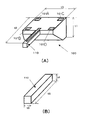
도 1의 (A), (B)는, 본 발명의 실시 형태에 따른 압전 소자로서의 진동형 자이로 센서 소자(100)를 나타내고 있고, 도 1의 (A)는 진동형 자이로 센서 소자(100)의 전체를 도시하는 외관 사시도, 도 1의 (B)는 진동형 자이로 센서 소자(100)의 진동자(110)만을 확대하여 도시하는 사시도이다. 이 진동형 자이로 센서 소자(100)는, 도 1의 (A), (B)에 도시한 바와 같이 실리콘 단결정 기판으로부터 잘라내어진, 소위 외팔보 형상의 진동자(110)를 구비하고 있다. 이 진동자(110)는, 길이 방향에 대하여 수직인 평면에서 절단했을 때의 단면 형상이 직각사변형으로 되는 사각주 형상으로 형성되어 있다. 1A and 1B show a vibrating
이 진동형 자이로 센서 소자(100)는, 그 대략적인 크기로서, 소자 두께 t1이 300㎛, 소자 길이 t2가 3 ㎜, 소자 폭 t3이 1 ㎜이다. 또한, 실제로 진동하는 진동보 즉 진동자(110)의 크기로서, 진동보 두께 t4를 100㎛, 진동보 길이 t5를 2.5 ㎜, 진동보 폭 t6을 100㎛으로 했다. 이 형상으로 진동보를 진동시킨 경우의 공진 주파수는 대략 40 ㎑ 전후로 된다. 이상의 수치는 일례이며, 사용하는 주파수, 목표로 하는 소자의 크기에 따라 임의로 설정 가능하다. This vibration type
진동형 자이로 센서 소자(100)는, 도시 생략된 IC 기판 상에 실장되어 사용된다. 이 IC 기판과 대향하는 쪽의 소자(100)의 실장면(저면)을 도 2에 도시한다. The vibration type
진동자(110)의 표면에는, 기준 전극(104a), 압전체(105a)가 순서대로 적층되어 있다. 압전체(105a)의 상에는, 구동 전극(106a)와 한쌍의 검출 전극(106b, 106c)가 진동자(110)의 길이 방향을 따라 상호 평행하게 또한 접촉하지 않도록 각각 형성되어 있다. 구동 전극(106a), 검출 전극(106b, 106c) 및 기준 전극(104a)에는, 각각 배선 접속 단자(101A, 101B, 101C, 101D)가 설치되어 있다. On the surface of the
압전체(105a)는, 예를 들면, 티탄산지르콘산 납(PZT) 등의 압전 세라믹스나, 수정, LaTaO3 등의 압전 단결정 등으로 이루어지는 압전막이다. 기준 전극(104a), 구동 전극(106a) 및 검출 전극(106b, 106c)는, 금속 전극 혹은 도전성 산화물 전극 등으로 이루어진다. 또한, 기준 전극(104a)는 본 발명의 「제1 전극막」에 대응하고, 구동 전극(106a) 및 검출 전극(106b, 106c)는 본 발명의 「제2 전극막」에 대응한다. The
이 진동형 자이로 센서 소자(100)는, 도 3에 도시하는 IC 회로(40)에 접속됨으로써 동작하고, 각속도에 따라서 발생하는 코리올리력을 검출하는 각속도 센서(진동형 자이로 센서)로서 기능한다. IC 회로(40)는, 진동형 자이로 센서 소자(100)가 실장되는 IC 기판 상에 동시에 탑재된 IC 회로 소자나 다른 전자 부품으로 구성된다. This vibration type
IC 회로(40)는, 가산 회로(41)와, 증폭 회로(42)와, 위상 시프트 회로(phase-shift circuit)(43)와, AGC(Auto Gain Controller)(44)과, 차동 증폭 회로(45)와, 동기 검파 회로(46)와, 평활 회로(47)를 구비하고 있다. The
진동형 자이로 센서 소자(100)의 한쌍의 검출 전극(106b, 106c)는, 각각 가산 회로(41)와 차동 증폭 회로(45)과 접속된다. 또한, 진동형 자이로 센서 소자(100)의 구동 전극(106a)는, AGC(44)의 출력단과 접속된다. The pair of
이 각속도 센서에서는, 가산 회로(41), 증폭 회로(42), 위상 시프트 회로(43), AGC(44) 및 진동형 자이로 센서 소자(100)에 의해서, 소위 위상 시프트 발진 회로가 구성되어 있다. 그리고, 이 위상 시프트 발진 회로에 의해서, 진동형 자이로 센서 소자(100)의 기준 전극(104a)와 구동 전극(106a) 사이에 전압이 인가되어, 진동자(110)를 자려 진동시킨다. 진동자(110)의 진동 방향은, 해당 진동자(110)의 두께 방향으로 된다. In this angular velocity sensor, what is called a phase shift oscillation circuit is comprised by the
또한, 이 각속도 센서에서는, 한쌍의 검출 전극(106b, 106c)가 가산 회로(41) 및 차동 증폭 회로(45)에 접속되고, 차동 증폭 회로(45)의 출력단이 동기 검파 회로(46)에 접속되고, 이 동기 검파 회로(46)가 평활 회로(47)에 접속되어 있고, 이들과 압전체(105a)에 의해, 진동자(110)의 각속도를 검출하는 검출부로서 기능한다. In this angular velocity sensor, a pair of
즉, 진동형 자이로 센서 소자(100)의 진동자(110)를 전술한 위상 시프트 발진 회로에서 자려 진동시키고 있을 때에, 진동자(110)의 길이 방향의 주위에 각속도가 발생하면, 코리올리력에 의해 진동자(110)의 진동 방향이 변화한다. 이 경우, 검출 전극(106b, 106c)의 한 쪽의 출력은 증가하고, 다른 쪽의 출력은 감소한다. 어느 하나의 출력 혹은 양 출력의 변화량을 IC 회로(40)에 의해 검출 측정하여, 진동자(110)의 길이 방향의 주위의 입력 각속도를 검출한다. That is, when the
다음으로, 이상과 같이 구성되는 본 실시 형태의 진동형 자이로 센서 소자(100)의 한 제조예를 설명한다. 도 4는, 진동형 자이로 센서 소자(100)의 제조 방법을 설명하는 주요 공정 플로우이다. Next, an example of manufacture of the vibration type
[기판 준비 공정]Board Preparation Process
우선, 도 5의 A, B에 도시하는 것 같은 Si 기판(1)을 준비한다. 기판(1)의 크기는, 소유하는 박막 프로세스의 라인에 따라서 임의로 설정되고, 본 실시 형태로서는 직경이 4인치의 웨이퍼를 이용했다. 기판(1)의 두께는, 작업성이나 코스트에 의해 결정되지만, 최종적으로 진동자의 두께 이상이면 되고, 본 실시 형태에서는 300㎛의 두께로 했다. First, the
이 Si 기판(1)의 양면에는, 이방성 습식 에칭시의 보호 마스크로 되는 열산화막(SiO2막)(2A, 2B)를 형성해 둔다. 열산화막(2A, 2B)의 막 두께는 임의이지만, 본 실시 형태로서는 0.3㎛ 정도로 했다. 또한, Si 기판(1)에 관해서는 N형을 채용하고 있지만, 그 선택은 임의이다. Si 기판(1)의 방위면은, 도 5의 A에서 도시하는 기판 광구면이 (100) 방위면, 기판(1)의 단면으로 되는 도 5의 B의 면이 (110)면으로 되도록 기판의 잘라내기가 행해지고 있다. On both surfaces of the
[다이어프램 형성 공정]Diaphragm Formation Process
다음으로, 도 6의 A, B에 도시한 바와 같이 기판(1)의 이면의 열산화막(2B)의 일부를 제거하기 위해, 제거할 부분을 개구부로 하는 레지스트 패턴막(3)을 형성한다. 이 레지스트 패턴막(3)의 형성 방법은, 통상의 반도체 박막 형성 프로세 스에서 이용되는 포토리소그래피 기술을 이용하고 있다. 레지스트재는, 예를 들면 동경 오우카 사제 OFPR-8600를 이용했지만, 종류는 이것에 한정되지 않는다. 포토리소그래피의 공정은, 레지스트재 도포·프리베이킹·노광·현상이라는 일반적으로 박막 공정에서 이용되는 기술이며, 여기서는 상세 내용은 생략한다. 또한, 이 후의 프로세스에 있어서도 포토리소그래피 기술을 이용하고 있지만, 특수한 사용 방법을 제외하고 일반적인 공정에 관해서는 생략한다. Next, as shown in FIGS. 6A and 6B, in order to remove a part of the
도 6의 A에서 도시하는 개구부의 각각이 1개의 소자로 된다. 개구부의 형상은 최종적인 보 형상과 기판(1)의 두께, 및 보 형상(진동자(110))를 형성할 때의 에칭 폭(도 34 및 도 35에서 부호 표시하는 t7)로 결정된다. 에칭 폭 t7에 대해서는 후술하지만, 여기서는 200㎛으로 했다. Each of the opening portions shown in FIG. 6A is one element. The shape of the opening is determined by the final beam shape, the thickness of the
개구부의 폭 방향(다이어프램 폭 t9)에 관해서, 필요한 폭은, 우선 진동보 폭 t6+에칭 폭 t7×2(좌우분)이다. 또한, 기판(1)의 두께가 300㎛에서 진동보 두께가 100㎛이며, 후술하지만 습식 에칭의 방법으로 기판 두께 300㎛을 진동보 두께100㎛까지 깍는 경우, 도 9에 도시한 바와 같이 다이어프램 깊이 t10는 200㎛이며, 이 때 θ1= 55°의 각도를 갖고 깎이는 특징이 있다. 이 때문에 그 만큼의 폭: t10×1/tan55°= 140㎛을 좌우분 더해둘 필요가 있다. 결국 다이어프램 폭 t9= t6+t7×2+140×2= 100+200×2+140×2= 780㎛로 된다. 마찬가지로 다이어프램 길이 t8= 진동보 길이 t5+보 공간격 t7+140×2= 2500+200+140×2= 2980㎛으로 된다. Regarding the width direction (diaphragm width t9) of the opening portion, the necessary width is first the oscillation beam width t6 + etching width t7 × 2 (left and right). Moreover, when the thickness of the board |
다음으로, 도 7의 A, B에 도시한 바와 같이 상기의 개구 부분에 상당하는 부분의 열산화막(2B)를 제거한다. 제거의 방법은 이온 에칭 등의 물리적 에칭이어도 되고, 습식 에칭이어도 되지만, 기판(1)의 계면의 평활성을 고려하면 열산화막(2B)만이 제거되는 습식 에칭이 바람직하다. 본 실시 형태로서는 습식 에칭의 약액으로서 불화암모늄을 이용했다. 단, 습식 에칭인 경우 장시간 에칭을 행하면 개구 부분의 측면으로부터 에칭이 진행하는 소위 사이드 에칭이 커지기 때문에, 열산화막(2B)의 개구 부분만이 제거된 시점에 에칭을 종료시킬 필요가 있다. Next, as shown to A and B of FIG. 7, the
다음으로, 도 8의 A, B 및 도 9에 도시한 바와 같이 개구 부분으로서 노출된 기판(1)에 대하여 습식 에칭을 실시함으로써, 개구 부분의 기판(1)의 두께를 원하는 진동보 두께 t4가 될 때까지 깎는다. 본 실시 형태로서는 Si인 기판(1)을 에칭하기 위해서 TMAH(수산화 테트라메틸암모늄) 20% 용액을 이용하고 있다. 이 때, 액 온도를 80℃로 유지하여 침지 에칭을 행하고 있다. Next, wet etching is performed on the
도 9는 도 8의 B의 W 부분을 확대하여 나타낸 것이다. 상기의 조건으로 에칭량(다이어프램 깊이) t10를 200㎛으로 하기 위해서, 대략 6 시간의 에칭을 행하였다. 또한, 이 에칭에 의해 개구 부분의 기판(1)의 형상은, 도 9에 도시한 바와 같이 단부가 습식 에칭 각도 θ1(= 55°)를 갖고 형성된다. 또한, 이러한 습식 에칭 약액으로서 TMAH 이외에 KOH(수산화칼륨)이나 EDP(에틸렌 디아민-피로카테콜 물) 용액 등이 사용할 수 있는데, 본 실시 형태로서는 열산화막(2A, 2B)와의 에칭 레이트의 선택비가 보다 커지는 TMAH를 채용했다. FIG. 9 is an enlarged view of a portion W of FIG. 8B. In order to make etching amount (diaphragm depth) t10 into 200 micrometers on the above conditions, etching was performed for about 6 hours. In addition, by the etching, the shape of the
그런데, 본 실시 형태로서는 진동보 두께가 되기까지의 기판 연삭에 Si의 특징을 살린 습식 에칭을 채용하고 있지만, 연삭의 방법은 임의이며 이 방법에 한정되는 것이 아니다. By the way, in this embodiment, although the wet etching which utilized the characteristic of Si was employ | adopted for the grinding of the board | substrate until it becomes a vibration beam thickness, the method of grinding is arbitrary and is not limited to this method.
상기의 방법에 의해 상기 개구 부분 내에 다이어프램이 형성된다. 습식 에칭에 의해 남겨진 다이어프램 두께 t11가 최종적으로 진동보 두께 t4와 동등하게 된다. The diaphragm is formed in the opening portion by the above method. The diaphragm thickness t11 left by wet etching is finally equal to the beam thickness t4.
또한, 이후의 설명에서는, 도 8의 A, B에 W로 나타낸 1개의 소자를 확대하여 설명한다. 또한, 도면에서는 설명을 알기 쉽게 하기 위해서, 실제의 치수비와는 다른 경우도 있다. 또한, 도 10의 A, B에 도시한 바와 같이 이후에는 상기까지 형성한 다이어프램의 개구부 및 열산화막(2B)를 아래쪽으로 하여 설명한다. In addition, in the following description, one element shown by W to A and B of FIG. 8 is expanded and demonstrated. In addition, in drawing, in order to make description easy to understand, it may differ from actual dimension ratio. In addition, as shown to A and B of FIG. 10, the opening of the diaphragm formed above and the
[전극막 형성 공정][Electrode Film Forming Step]
다음으로, 도 10의 A, B에 도시한 바와 같이 하층 전극막(4), 압전막(5), 상부 전극막(6)을 형성한다. 하층 전극막(4)은 「제1 전극막」에 대응하고, 상부 전극막(6)은 「제2 전극막」에 대응한다. 하층 전극막(4)은, 압전막의 특성을 향상시키기 위해서, 기초막으로서 Ti(티탄)막(막 두께 20 ㎚)와, 이 Ti 막의 상에 형성한 Pt(백금)막(막 두께 100 ㎚)로 이루어지는 적층막으로 했다. 또한, Pt 이외에 Au나 Rh(로듐), Re(레늄) 등의 다른 금속막이 적용 가능하고, Ti 이외에 Ta(탄탈) 등도 적용 가능하다. Next, as shown to A and B of FIG. 10, the
하층 전극막(4)의 형성 공정에서는, 우선, 마그네트론 스퍼터 장치로 Ti를 20 ㎚ 성막하고, 상기 Ti 상에 Pt를 100 ㎚ 성막했다. Ti 및 Pt은, 가스압 0.5 Pa에서 각각 1 ㎾ 및 0.5 ㎾의 RF(Radio Frequency) 파워(고주파 전력)으로 성막했다. 티탄산지르콘산 납의 기초막으로서, Pt 막이 사용되고 있지만, 그 밀착성을 높이는 것을 목적으로 하여 Ti가 성막된다. In the formation process of the
다음으로, 압전막(5)을 형성한다. 압전막(5)의 형성 공정에서는, 마그네트론 스퍼터 장치로 Pb1.02(Zr0.53Ti0.47)O3의 산화물 타깃을 이용하여, 상온, 산소 가스압을 0.2∼3 Pa, RF 파워 0.1∼5 ㎾의 조건으로 압전막(5)을 1.4㎛ 성막했다. 또한, 압전막(5)의 형성 방법의 상세에 대해서는 후술한다. Next, the
그리고, 상부 전극막(6)의 형성 공정에서는, 전술된 바와 같이 하여 형성된 압전막(5)의 표면에 Pt를 200 ㎚ 성막했다. 상기 Pt는 마그네트론 스퍼터 장치로 가스압 0.5 Pa, RF 파워 0.5 ㎾의 조건으로 성막했다. In the step of forming the
[압전막의 형성 방법][Formation of Piezoelectric Film]
본 실시 형태에서는, 압전막(5)의 형성 방법으로서, 압전막(5)의 형성 두께보다도 작은 층두께의 티탄산지르콘산 납으로 이루어지는 압전체 박막을 성막하는 성막 공정과 그 압전체 박막을 열처리하여 결정화시키는 결정화 열처리(어닐링)공정을 복수회 반복하여 행함으로써, 소정 두께의 압전막(5)을 형성한다. 이에 따라 층두께 방향으로 균일한 결정성을 갖는 압전막(5)을 제작하도록 하고 있다. In this embodiment, as a method of forming the
성막 공정에서는, 압전체 박막의 적층 횟수를 7회로 하고 200 ㎚을 단위 층두께로 했다. 결정화 열처리 공정에서는, 전기로를 이용하여 산소 분위기 하에서 700℃ 이상 800℃ 이하의 온도에서 30분간 행하였다. In the film forming step, the number of laminations of the piezoelectric thin film was set to seven times and 200 nm was used as the unit layer thickness. In the crystallization heat treatment step, an electric furnace was used for 30 minutes at an temperature of 700 ° C. to 800 ° C. under an oxygen atmosphere.
종래의 압전 소자는, 목적으로 하는 압전 특성이 얻어지는 두께의 압전막을 일시에 성막한 후, 어닐링 처리를 행하고 있었다. 그러나, 예를 들면 1㎛ 이상의 두께로 압전막을 일시에 성막한 경우, 어닐링 처리를 행하여도 압전막의 결정 배향성을 층두께 방향으로 균일화하는 것은 어려웠다. 이 때문에, 본 발명에서는, 전 술한 바와 같이, 결정화된 복수의 압전체 박막을 적층함으로써 압전막(5)을 형성함으로써, 압전막(5)의 결정성을 높이도록 하고 있다. 이에 의해, 압전 특성을 향상시킬 수 있음과 함께, 후술하는 바와 같이 압전막(5)의 가공 공정에서 패터닝 정밀도를 높여 수율의 향상을 도모하는 것이 가능하게 된다. In the conventional piezoelectric element, the piezoelectric film of the thickness in which the target piezoelectric characteristic is obtained is formed into a film at one time, and has performed the annealing process. However, in the case where the piezoelectric film was formed at a time with a thickness of, for example, 1 µm or more, it was difficult to uniformize the crystal orientation of the piezoelectric film in the layer thickness direction even after annealing treatment. For this reason, in the present invention, as described above, the
도 11의 A는, 압전체 박막(티탄산지르콘산 납)의 적층 총두께를 1.4㎛으로 한 경우의 압전체 박막의 단위층 당의 막 두께를 변화시켰을 때의 양품율(웨이퍼 수율)을 나타내는 한 실험 결과이다. 또한, 도 11의 B는, 도 11의 A의 각 점에서의 단위층 막 두께와 양품율과의 관계를 나타내고 있다. 여기서의 양품율의 열화는, 압전 특성의 열화에 의한 것이다. 압전체 박막의 1회 당의 막 두께가 작을 수록(예를 들면 100 ㎚×14회, 200 ㎚×7회) 양품율은 높은 것을 알 수 있다. 또한, 350 ㎚의 압전체 박막의 4회 적층을 초과하면 양품율은 크게 저하하기 시작한다. 고로, 압전체 박막의 단위 적층 막 두께는, 350 ㎚ 이하가 바람직하다. FIG. 11A is an experimental result showing the yield (wafer yield) when the film thickness per unit layer of the piezoelectric thin film is changed when the total thickness of the piezoelectric thin film (lead zirconate titanate) is set to 1.4 µm. . In addition, B of FIG. 11 has shown the relationship between the unit layer film thickness and the yield ratio in each point of A of FIG. The deterioration of the yield ratio here is due to the deterioration of the piezoelectric characteristics. It turns out that the yield is so high that the film thickness per once of a piezoelectric thin film is small (for example, 100 nm x 14 times, 200 nm x 7 times). In addition, when the stacking time of the 350 nm piezoelectric thin film is exceeded four times, the yield rate starts to significantly decrease. Therefore, as for the unit laminated film thickness of a piezoelectric thin film, 350 nm or less is preferable.
또한, 압전체 박막의 적층 총두께는 상기의 예에 한정되지 않고, 단위층 당의 막 두께가 350 ㎚ 인 경우, 압전체 박막의 적층 총두께가 1㎛일 때는 3층, 또한, 적층 총두께가 700 ㎚일 때는 2층으로 된다. In addition, the lamination total thickness of a piezoelectric thin film is not limited to the said example, When the film thickness per unit layer is 350 nm, when the lamination total thickness of a piezoelectric thin film is 1 micrometer, three layers and the lamination total thickness are 700 nm It becomes two levels when.
한편, 티탄산지르콘산 납은, 성막 중에 산소 결손이 발생하기 쉬워, 막 내의 도입 산소량이 적으면 절연성이 열화하여 양호한 압전 특성을 나타내지 않게 된다. 그래서 본 실시 형태에서는, 티탄산지르콘산 납으로 이루어지는 압전체 박막을 산소 가스 분위기 속에서 성막하고 있다. 여기서 말하는 산소 가스 분위기란, 산소 가스와 불활성 가스(아르곤 등)와의 혼합 가스 분위기 또는 순수한 산소 가스 분위 기를 의미한다. On the other hand, lead zirconate titanate tends to cause oxygen vacancies during film formation, and when the amount of oxygen introduced into the film is small, the insulation deteriorates and the piezoelectric properties are not exhibited. Therefore, in this embodiment, a piezoelectric thin film made of lead zirconate titanate is formed in an oxygen gas atmosphere. Oxygen gas atmosphere here means the mixed gas atmosphere of oxygen gas and an inert gas (argon etc.), or pure oxygen gas atmosphere.
표 1은, 티탄산지르콘산 납의 성막 조건에서, 산소, 아르곤의 혼합 비율을 변화시켜 성막한 압전막을 갖는 진동자의 진동 진폭을 나타내고 있다. 진폭의 값이 클수록 양호한 압전 특성을 갖고 있고, 진폭의 크기가 35㎛ 이상인 진동자를 양품 레벨의 샘플로 한다. 일반적으로 코리올리력의 검출 감도는, 진동자의 질량 또는 진동자의 진폭이 클수록 좋다. 전술한 바와 같은 소자 형상 혹은 소자 치수를 갖는 본 실시 형태의 진동형 자이로 센서 소자(100)에서는, 질량의 증대에는 한계가 있기 때문에 진폭을 크게 설정하여 소정의 검출 감도를 얻도록 하고 있다. 이 예에서는, 소정의 검출 감도가 얻어지는 진폭의 하한을 35㎛로 하고 있다. Table 1 shows the vibration amplitude of the vibrator having the piezoelectric film formed by changing the mixing ratio of oxygen and argon under the film forming conditions of lead zirconate titanate. The larger the value of the amplitude, the better the piezoelectric characteristics and the amplitude of the oscillator having a magnitude of 35 µm or more are used as samples of good quality. In general, the detection sensitivity of the Coriolis force is better as the mass of the vibrator or the amplitude of the vibrator is larger. In the vibration type

이상의 점으로부터, 산소 가스 분압이 50% 이상으로 원하는 진동 특성이 얻어지는 압전 소자를 제작하는 것이 가능해지고, 특히 산소 가스 분압이 높을수록 양호한 진동 특성을 얻을 수 있다. From the above, it is possible to fabricate a piezoelectric element in which the desired vibration characteristics are obtained at an oxygen gas partial pressure of 50% or more, and in particular, the higher the oxygen gas partial pressure, the better vibration characteristics can be obtained.
또한, 산소 가스100% 분위기 속에서의 압전체 박막의 성막에서는, 타깃의 Pb 함유량이 중요하다. 표 2에 도시한 바와 같이 Pb량이 Zr/Ti에 대하여 1.01인 경우, 형성되는 압전막은, 압전 특성을 나타내는 페로브스카이트상이 아닌, 파이로클로어상이 석출하여 압전 특성이 열화하는 것을 알 수 있었다. In the film formation of the piezoelectric thin film in an

또한, 표 3에 나타낸 바와 같이 Pb량이 1.2 이상으로 지나치게 들어 간 타깃을 이용하면, 절연성을 나타내는 유전 손실의 값이 증가한다. 이것은, 티탄산 지르콘산 납의 막 구조가 성기게 되기 때문이다. Moreover, as shown in Table 3, when the target which Pb amount exceeded 1.2 or more is used, the value of dielectric loss which shows insulation will increase. This is because the film structure of lead zirconate titanate becomes coarse.

계속해서, 도 12는, 어닐링 온도를 변화시킨 경우의 압전체 박막(티탄산 지르콘산 납)의 페로브스카이트상의 (111)면의 X선 회절의 강도를 측정한 결과를 나타내고 있다. X선 회절 강도는, X선 회절 패턴의 피크 강도를 나타내고 있다. 어닐링 온도가 700℃ 부근에서 회절 강도의 변화량이 완만하게 되기 시작하고 있다. 이것은, 어닐링 온도가 700℃ 이상으로 압전체 박막의 결정화가 거의 포화하고 있는 것을 의미하고 있다. 또한, 750℃ 이상으로 회절 강도가 재상승하고 있는 것은, 기초의 Pt층(하부 전극막)의 결정화가 진행됨에 따라 압전체 박막의 결정성이 영향을 받고 있는 것을 나타내고 있다. 12 shows the result of measuring the intensity of X-ray diffraction of the (111) plane of the perovskite phase of the piezoelectric thin film (lead zirconate titanate) when the annealing temperature is changed. X-ray diffraction intensity represents the peak intensity of the X-ray diffraction pattern. When the annealing temperature is around 700 ° C, the amount of change in the diffraction intensity starts to slow down. This means that the crystallization of the piezoelectric thin film is almost saturated at annealing temperature of 700 ° C or higher. Incidentally, the fact that the diffraction intensity has risen above 750 ° C indicates that the crystallinity of the piezoelectric thin film is affected as the crystallization of the underlying Pt layer (lower electrode film) proceeds.
또한, 도 13에 압전체 박막의 막 두께 변화와 결정화 어닐링 시의 기판 이면의 온도가 관계를 나타낸다. 점선은 기판 표면의 온도 제어용의 열전쌍의 설정값(780℃)을 나타내고 있다. 기판 표면의 티탄산 지르콘산 납의 막 두께에 따라 기판 이면의 온도가 상이하다. 이것은 표면의 티탄산 지르콘산 납의 색이 막 두께에 따라서 변화하고, 적외선의 흡수율이 다르기 때문이다. 따라서, 막 두께가 상이한 압전막을 성막한 경우에는 실제의 어닐링 온도가 변화한다. 따라서, 본 실시 형태에서는, 상기 결정화 어닐링 처리 시에 기판 이면의 온도를 이용하여 온도 제어하도록 하고 있다. 13 shows the relationship between the film thickness change of the piezoelectric thin film and the temperature of the back surface of the substrate during crystallization annealing. The dotted line indicates the set value (780 ° C.) of the thermocouple for temperature control on the substrate surface. The temperature on the back surface of the substrate differs depending on the film thickness of lead zirconate titanate on the substrate surface. This is because the color of lead zirconate titanate on the surface changes depending on the film thickness, and the absorption of infrared rays is different. Therefore, when a piezoelectric film having a different film thickness is formed, the actual annealing temperature changes. Therefore, in this embodiment, temperature control is performed using the temperature of the back surface of a board | substrate at the time of the said crystallization annealing process.
도 14는 어닐링 온도를 변화시킨 경우의 양품율(웨이퍼 수율)을 나타내고 있다. 여기서의 양품율은, 1매의 웨이퍼로부터 제작되는 복수의 소자 중 소정의 압전 특성을 구비하는 소자의 비율을 의미한다. 어닐링 온도가 700℃ 이하에서는 양품율이 악화되고 있다. 이것은, 티탄산 지르콘산 납의 결정화가 불충분하기 때문에 압전 특성이 열화하고 있기 때문이라고 생각된다. 반대로, 어닐링 온도가 800℃ 부근에서는 양품율을 열화시키는 경향이 있다. 이것은, 파이로클로어상의 석출이 원인이라고도 생각되지만, 압전막의 에칭 잔류가 발생하여 양품율을 저하시키고 있기 때문이기도 하다. 도 14의 결과로부터, 어닐링 온도의 최적 범위는 700℃ 이상 800℃ 이하, 바람직하게는 700℃ 이상 750℃ 이하, 더욱 바람직하게는 725℃ 이상 750℃ 이하의 범위이다. 14 shows the yield (wafer yield) when the annealing temperature is changed. The yield ratio here means the ratio of the element which has a predetermined piezoelectric characteristic among the some elements manufactured from one wafer. If annealing temperature is 700 degrees C or less, a yield will deteriorate. This is considered to be because piezoelectric properties deteriorate because crystallization of lead zirconate titanate is insufficient. On the contrary, when annealing temperature is around 800 degreeC, there exists a tendency for deterioration of a yield. Although this is considered to be the cause of precipitation of a pyroclaw phase, it is also because etching residual of a piezoelectric film | membrane generate | occur | produces and the yield is reduced. From the result of FIG. 14, the optimum range of annealing temperature is 700 degreeC or more and 800 degrees C or less, Preferably it is 700 or more and 750 degrees C or less, More preferably, it is the range of 725 degreeC or more and 750 degrees C or less.
이상과 같이, 티탄산 지르콘산 납의 어닐링 온도는 700℃ 이상 800℃ 이하가 바람직하다. 또한, 이 어닐링 처리는, 산소 가스 분위기 속에서 행해지는 것이 바람직하다. As described above, the annealing temperature of the lead zirconate titanate is preferably 700 ° C or more and 800 ° C or less. In addition, it is preferable that this annealing process is performed in oxygen gas atmosphere.
[전극막 가공 공정] Electrode Film Processing Process
다음으로, 도 15의 A, 도 15의 B에 도시한 바와 같이 성막한 상부 전극막(6)을 소정 형상으로 가공한다. 상부 전극막(6)은 도 15의 A로 나타낸 바와 같이 3개의 부분으로 분리된다. 그 중 중심이 진동 보를 구동시키는 동력을 발생시키기 위한 구동 전극(6a)이며, 그 좌우에 코리올리력을 검출하기 위한 검출 전극(6b, 6c)이 설치된다. 구동 전극의 폭 방향 중심이 진동 보의 중심과 일치하고, 좌우의 검출 전극은 대칭으로 형성된다. 상부 전극막(6)의 직선 부분의 단부에는 배선 접속 부분이 설치되어 있다. Next, as shown in FIG. 15A and FIG. 15B, the
본 실시 형태에서는 구동 전극 폭 t13을 50㎛, 검출 전극 폭 t14를 10㎛, 상부 전극 길이 t12를 2㎜, 구동 전극(6a)과 검출 전극(6b, 6c) 사이는 5㎛로 했다. 이 크기에 관해서는 임의이지만, 최종적인 진동 보의 크기의 범위 내에 받아들일 필요가 있다. 또한, 후술하는 배선 패턴과의 접속 부분에 관해서의 형상도 임의이며, 본 실시 형태에서는 접속부 폭 t16을 50㎛, 접속부 길이 t15를 50㎛로 했다. In this embodiment, drive electrode width t13 was 50 micrometers, detection electrode width t14 was 10 micrometers, upper electrode length t12 was 2 mm, and the
상부 전극막(6)의 가공 방법으로서는, 포토리소그래피 기술을 이용하여 원하는 레지스트 패턴막을 형성한 후, 이온 에칭에 의해 불필요한 부분의 상부 전극막(6)을 제거했다. 상부 전극막(6)의 가공 방법에 관해서는 특별히 한정되는 것은 아니다. As the processing method of the
다음으로, 도 16의 A, 도 16의 B에 도시한 바와 같이 압전막(5)을 소정 형상으로 가공한다. 압전막(5)은 상부 전극막(6)을 완전하게 피복하는 형태이면, 형상은 임의이다. 본 실시 형태에서는 압전막 길이 t17을 2.2㎜, 압전막 폭 t18을 90㎛로 했다. 여기서, 압전막 폭의 중심을 진동 보의 중심과 일치시킨다. 압전막 폭 t18은 진동 보의 폭 t4 이하의 폭일 필요가 있다. 또한, 상부 전극막(6)의 외주보다 5㎛의 폭을 갖게 하여 압전막(5)을 가공했다. 이 폭에 관해서는 소자 전체의 형상 사이즈에 의해 임의로 설정된다. Next, as shown in FIG. 16A and FIG. 16B, the
또한, 본 실시 형태에서는, 전술한 바와 같이 티탄산 지르콘산 납의 기초막(하층 전극막)으로서 Pt막이 사용되고 있지만, 이 Pt막과 실리콘 기판과의 밀착성을 높이는 것을 목적으로 하여, Ti막이 성막되어 있다. 여기서, Ti막의 막 두께를 변화시켜, 260℃(10분간)의 크린 오븐을 이용하여 압전 소자의 에이징 시험을 행하였다. 그 결과, 도 17에 도시한 바와 같이 Ti막 두께가 얇아질수록 에이징 시험 전후에서의 압전 변위의 변화는 적었다. 그런 까닭으로 사용 환경의 온도 변화에 대하여 둔감한 압전 소자가 되어, 고온에서의 사용에 대하여도 신뢰성이 높은 압전 소자의 제작이 가능하게 된다. In the present embodiment, as described above, a Pt film is used as the base film (lower electrode film) of lead zirconate titanate, but a Ti film is formed for the purpose of improving the adhesion between the Pt film and the silicon substrate. Here, the film thickness of Ti film was changed and the aging test of the piezoelectric element was done using the clean oven of 260 degreeC (10 minutes). As a result, as shown in Fig. 17, the thinner the Ti film thickness, the smaller the change in piezoelectric displacement before and after the aging test. Therefore, it becomes a piezoelectric element insensitive to the temperature change of a use environment, and it becomes possible to manufacture the piezoelectric element with high reliability also in use at high temperature.
도 17은 Ti막 두께와 소자의 압전 변위와의 관계를 나타내고 있다. 도 17에 도시한 바와 같이 Ti층의 막 두께가 50㎚를 초과하면 압전 변위가 급격히 감소한다. 도 18은 Ti층의 막 두께와 양품율(웨이퍼 수율)의 관계를 나타내고 있다. Ti층의 막 두께가 5㎚ 이상 20㎚ 이하의 범위에서 높은 양품율이 얻어지고 있다. 이것은, 상기 범위에서 Ti층을 형성함으로써, 압전막의 결정 배향성이 높아지고, 에칭에 의한 패터닝 가공을 고정밀도로 행할 수 있는 것에 있다. 17 shows the relationship between the Ti film thickness and the piezoelectric displacement of the device. As shown in Fig. 17, when the film thickness of the Ti layer exceeds 50 nm, the piezoelectric displacement decreases rapidly. 18 shows the relationship between the film thickness of the Ti layer and the yield (wafer yield). High yield is obtained in the range whose film thickness of a Ti layer is 5 nm or more and 20 nm or less. This is because crystal orientation of a piezoelectric film becomes high by forming a Ti layer in the said range, and the patterning process by an etching can be performed with high precision.
한편, Ti층의 막 두께가 5㎚ 미만 혹은 20㎚초로 수율이 저하하는 이유는, 압전막의 결정 배향성이 저하하여 티탄산 지르콘산 납의 Zr 성분이 에칭되지 않고서 남아 있는 것에 있다. 그 결과, 하층 전극막의 에칭 시에 해당 Zr의 에칭 잔류가 커버제(마스크)로서 기능하여, 원하는 형상으로 전극 패턴을 형성하지 않고 전극 사이에서 단락을 발생시킨다. On the other hand, the reason why the film thickness of the Ti layer decreases to less than 5 nm or 20 nm sec is that the crystal orientation of the piezoelectric film is lowered and the Zr component of lead zirconate titanate is not etched. As a result, the etching residual of this Zr functions as a cover agent (mask) at the time of the etching of a lower electrode film, and a short circuit is generated between electrodes without forming an electrode pattern in a desired shape.
압전막(5)의 가공 방법으로서는, 포토리소그래피 기술을 이용하여 압전부 형상의 레지스트 패턴막을 형성한 후, 본 실시 형태에서는 불화 질산 용액에 의한 습식 에칭에 의해 제거했다. 제거의 방법에 관해서는 임의이며, 물리적인 이온 에칭에 의한 제거나, 화학적으로 RIE(Reactive Ion Etching)에 의해 제거하는 방법이 생각된다. As the processing method of the
다음으로, 도 19의 A, 도 19의 B에 도시한 바와 같이 하층 전극막(4)을 소정 형상으로 가공한다. 이 하층 전극막(4)은 압전막(5)을 완전하게 피복하는 형태이면 형상은 임의이다. 본 실시 형태에서는 하층 전극 길이 t19를 2.3㎜, 하층 전극 폭 t20을 94㎛로 했다. 여기서, 하층 전극 폭의 중심은 진동 보의 중심과 일치시킨다. 하층 전극 폭 t20은 진동 보의 폭 t4 이하의 폭일 필요가 있다. 또한, 압전막(5)의 외주보다 5㎛의 폭을 갖게 하여 하층 전극막(4)을 가공했다. 이 폭에 관해서는 소자 전체의 형상 사이즈에 의해 임의로 설정된다. 또한, 하층 전극막(4)에 대하여 외부와의 전기적 접합을 도모하기 위해서, 도 19의 A에 도시한 바와 같이 하층 전극 접합 부분(4A)을 형성한다. 하층 전극 접합부(4A)는, 이 후 배선 패턴으로 인출할 수 있는 면적을 확보할 필요가 있어, 하층 전극 접합부 길이 t21을 200㎛, 하층 전극 접합부 폭 t22를 100㎛로 했다. Next, as shown in FIG. 19A and FIG. 19B, the
이상의 하층 전극막(4)의 가공 방법으로서는, 포토리소그래피 기술을 이용하여 하층 전극부 형상의 레지스트 패턴막을 형성한 후, 이온 에칭에 의해 불필요 부분을 제거했다. 이 가공 방법에 관해서도 임의이며, 이온 에칭에 한정되는 것은 아니다. As a method of processing the lower
[배선막 형성 공정] [Wired film formation process]
다음으로, 도 20 및 도 21에 도시한 바와 같이 배선 기초막(7)을 형성한다. 이 목적은, 후술하는 배선막(9)의 밀착성을 확보하기 위해서이다. 배선 기초막(7)은 절연 재료가 전제로 된다. 배선 기초막(7)은 진동자 상, 각 전극 접속부(6a, 6b, 6c), 진동자 주변의 에칭 영역 이외에 성막되어 있으면, 그 형상은 임의이다. 본 실시 형태에서는 전극막의 밀착성 향상도 겸하여, 상부 전극막(6), 하층 전극막(4)의 각각과 배선 기초막(7)을 5㎛의 중첩을 갖게 하는 것으로 했다. Next, as shown in FIG. 20 and FIG. 21, the
배선 기초막(7)의 형성 방법은, 포토리소그래피 기술에 의해 원하는 형상을 개구부로 하는 레지스트 패턴막을 형성한 후, 배선 전극막을 스퍼터링에 의해 성막하여, 불필요한 부분에 부착한 스퍼터링막을 레지스트 패턴막의 제거와 동시에 제거하는 소위 리프트오프의 방법을 이용했다. 재료는 알루미나를 선정하여, 75㎚ 퇴적시켰다. 단, 이 배선 기초막(7)의 재료 및 형성 방법은 임의이며, 상기의 형성 방법 및 재료에 한정되는 것은 아니다. In the method of forming the
다음으로, 도 22 및 도 23에 도시한 바와 같이 전극 접속부(6a, 6b, 6c)에 평탄화 레지스트막(8)을 형성한다. 이 평탄화 레지스트막(8)은 후술하는 배선막(9)과 상부 전극막(6)과의 전기적 접속을 원활히 행하는 것이 목적이다. 배선막(9)과 상부 전극막(6)을 물리적으로 접합할 때에, 압전막(5)과 하층 전극막(4)의 단부를 통과하지 않을 수 없지만, 압전막(5)에 관해서는 본 실시 형태에서는 습식 에칭에 의해 형성하고 있어 그 단부는 역테이퍼 내지는 거의 수직 상태로 되고 있고 평탄화 레지스트막(8)을 설치하지 않고서 배선을 행하면 그 단부에서 단선할 우려가 있다. 또한, 하층 전극막(4)이 노출되어 있기 때문에 평탄화 레지스트막에 의해 절연을 취하지 않으면 전기적으로 단락한다. 이상의 관점으로부터 평탄화 레지스트막(8)을 설치하고 있다. Next, as shown in FIG. 22 and FIG. 23, the planarization resist
평탄화 레지스트막(8)의 형상은, 후술하는 배선막(9)을 피복하는 형태이면 임의이며, 본 실시 형태에서는 평탄화 레지스트막 폭 t23을 200㎛, 평탄화 레지스트막 길이 t24를 50㎛로 했다. The shape of the planarization resist
평탄화 레지스트막(8)의 형성 방법은 포토리소그래피 기술에 의해 레지스트막을 원하는 형상으로 패터닝을 행한 후, 280∼300℃ 정도의 열 처리를 가함으로써 패터닝을 행한 레지스트막을 경화시킨다. 이 때, 본 실시 형태에서는 레지스트막의 두께를 2㎛ 정도로 했지만, 이 두께에 관해서는 압전막(5), 하층 전극막(4)의 두께에 따라서 변화시켜, 대략 양자의 두께의 합계 이상의 두께를 갖게 하는 것이 바람직하다. In the method of forming the planarization resist
본 실시 형태에서는 상기 평탄화 레지스트막(8)으로서 감광성 레지스트막을 이용하고 있지만, 이 재료에 관해서는 이것에 한정되는 것은 아니다. 상기의 목적에 맞는 비도전성의 재료이면 그 형성 방법도 포함시켜 임의이다. In this embodiment, although the photosensitive resist film is used as the said planarization resist
다음으로, 도 24 및 도 25에 도시한 바와 같이 상부 전극막(6)과 외부와의 접속을 꾀하기 위해 배선막(9)을 형성한다. 이것은 외부와의 전기적 접속을 쉽게 하기 위해서이며, 배선막(9)은 평탄화 레지스트막(8)의 상면을 통해 상부 전극막(6)의 접합부에 접속된다. 상부 전극 접속부(6a, 6b, 6c)의 형상은 임의이지만, 전기적인 접촉 저항을 감소시키기 위해서, 5㎛ 사방 이상의 크기가 바람직하다. 또한 본 실시 형태에서는 외부와의 전기적 접속에 관해서는 Au 범프의 플립 칩에 의한 접합 방법을 전제로 하고 있기 때문에, 도 24와 같이 각 전극에 대하여 전극 패드(101A, 101B, 101C, 101D)를 형성함으로써 Au 범프 영역을 확보하고 있다. Next, as shown in FIG. 24 and FIG. 25, the
전극 패드(101A, 101B, 101C, 101D)는 Au 범프의 형성이 가능한 면적이 필요하며, 본 실시 형태에서는 전극 패드부 길이 t25를 120㎛, 전극 패드 폭 t26을 120㎛로 했다. 또한, 상부 전극막(6)인 구동 전극(6a) 및 좌우의 검출 전극(6b, 6c), 하층 전극막(4)의 4개에 대하여 각각 외부와의 전기적인 접합이 필요해지기 때문에, 배선막(9)에 관해서도 이들 4개에 대하여 독립되어 있는 것이 필요하고, 전극 패드(101A, 101B, 101C, 101D)의 위치에 대해서는 소자 에리어 AR 내에 있는 것이 전제이다. The
또한, 이 공정에서 동시에 분극 레일도 형성한다. 본 실시 형태의 진동자는, 최종적으로 분극하여 압전 특성을 안정화시키지만, 그 분극 작업을 효율화하기 위해 동렬의 소자를 통합하여 행하는 것으로 하고 있다. 이 동시 분극을 행하기 위해서는 전압 인가측, GND측의 배선을 사전에 형성해 놓아야 하여, 여기서는, 도 26과 같이 각 분극 레일(111, 112)로서 가로 일직선으로 형성하고 있다. 이 시점에서는 소자와 레일은 독립하고 있지만, 후술하는 Cu 배선(11)의 형성으로 전압 인가측과 GND 측의 배선이 접속된다. In this process, a polarization rail is also formed at the same time. The vibrator of the present embodiment finally polarizes to stabilize the piezoelectric characteristics, but in order to make the polarization work more efficient, the vibrators are integrated and performed. In order to perform this simultaneous polarization, wirings on the voltage application side and the GND side must be formed in advance, and here, as shown in FIG. 26, the polarization rails 111 and 112 are formed in a horizontal straight line. At this point in time, the elements and the rails are independent, but the wirings on the voltage application side and the GND side are connected by forming the
배선막(9)의 형성 방법은, 포토리소그래피 기술에 의해 원하는 형상을 개구부로 하는 레지스트 패턴막을 형성한 후, 배선 전극막을 스퍼터링에 의해 성막하여, 불필요한 부분에 부착한 스퍼터링막을 레지스트막의 제거와 동시에 제거하는 소위 리프트오프의 방법에 의해 형성했다. 배선막의 재료로서는 부착력을 향상시키기 위해서 Ti를 20㎚ 퇴적시킨 후, 전기 저항이 낮고 저코스트의 Cu를 300㎚ 퇴적하고, 그 후 Au 범프와의 접합을 쉽게 하기 위해서 Au를 500㎚ 퇴적시켰다. 단, 이 배선막의 재료 및 형성 방법은 임의이며 상기의 형성 방법 및 재료에 한정되는 것은 아니다. In the formation method of the
[절연 보호막 형성 공정] [Insulation protective film formation process]
다음으로, 도 27 및 도 28에 도시한 바와 같이 진동 보 상 및 배선 상에 절연 보호막(10)을 형성한다. 이 목적은, 습도 등의 외적 요인에 의한 전극 사이 리크를 방지하는 것, 또한, 전극막의 산화를 방지하는 것이다. 진동자 상 보호막 폭 t27은 하층 전극 폭 t20보다도 넓고, 진동 보 폭 t6보다 좁은 것이 조건이며, 본 실시 형태에서는 t27을 98㎛로 했다. Next, as shown in Figs. 27 and 28, an insulating
진동자 상 보호막 길이 t28은 하층 전극 길이 t19보다도 넓고, 진동자 길이 t5보다 좁은 것이 조건이며, 본 실시 형태에서는 t28을 1.95㎜로 했다. 배선막(9) 상의 보호막(10)은, 전체를 피복하는 패턴이지만, Au 범프를 행하는 전극 패드 4 개소, 및 Cu 배선(11)과의 접속부 4 개소에서는, 선택적으로 보호막이 붙지 않도록 할 필요가 있다. The resonator upper protective film length t28 was wider than the lower electrode length t19, and was narrower than the resonator length t5. In this embodiment, t28 was 1.95 mm. Although the
보호막(10)의 형성 방법은, 포토리소그래피 기술에 의해 원하는 형상을 개구부로 하는 레지스트 패턴막을 형성한 후, 보호막을 스퍼터링에 의해 성막하여, 불필요한 부분에 부착한 스퍼터링막을 레지스트막의 제거와 동시에 제거하는 소위 리프트오프법의 방법에 의해 형성했다. 보호막(10)의 재료로서는, 부착력을 향상시키기 위해서 Al2O3을 50㎚ 퇴적시킨 후, 절연성이 높은 SiO2를 750㎚ 퇴적하고, 최상층에는 그 후의 진동 보 형성 시의 레지스트 밀착성을 향상시키기 위해서 Al2O3을 50㎚ 퇴적시켰다. 절연 보호막으로서 기능하는 SiO2는, 적어도 상부 전극의 두께의 2배 이상은 필요하지만, 1㎛ 이상의 두께로 되면 리프트 오프 시에 버어가 발생하기 쉽기 때문에, 본 실시 형태에서는 750㎚로 하고 있다. 또한, SiO2 성막 시에는 막 밀도를 높이기 위해서, Ar압을 방전 한계의 하한인 0.4Pa로 행하였다. In the method of forming the
다음으로, 도 29 및 도 30에 도시한 바와 같이 Cu 배선(11)을 형성한다. Cu 배선(11)은 상부 전극막(6)의 구동 전극(6a), 좌우의 검출 전극(6b, 6c)을 전압 인가측의 레일(111)에, 하층 전극(4)을 GND 측의 레일(112)에 각각 접속한다. Cu 배선(11)은, 도 31에 도시한 바와 같이 모든 소자로 마찬가지로 접속을 행한다. 이 배선을 Cu로 하는 이유는, 분극 후에 습식 에칭으로 용이하게 용해하여, 소자에 손상을 부여하는 일 없이 재차 소자를 독립할 수 있기 때문이다. 그 때문에, 소자에 손상을 부여하는 일 없이 용이하게 소실시킬 수 있는 도전체이면, 재료는 임의이다. 배선 폭 t29(도 33)는 분극 시의 도통을 확보하기 위해서, 30㎛ 이상이 바람직하다. Next, as shown in FIG. 29 and FIG. 30, the
Cu 배선(11)의 형성 방법은, 포토리소그래피 기술에 의해 원하는 형상을 개구부로 하는 레지스트 패턴막을 형성한 후, Cu를 스퍼터링에 의해 성막하여, 불필요한 부분에 부착한 스퍼터링막을 레지스트막의 제거와 동시에 제거하는 소위 리프트오프의 방법에 의해 형성했다. Cu 막 두께는 분극 시의 도통을 확보하기 위해서, 400㎚로 했다. 이 배선막의 형성 방법은 임의이며 상기의 형성 방법에 한정되는 것은 아니다. In the method for forming the
다음으로, 도 32에 도시한 바와 같이 이면 스토퍼막(12)을 형성한다. 그 목적은, 후술의 진동 보 형성으로 관통 에칭을 했을 때, 최하면의 플라즈마 집중에 의한 엣지 형상 불량을 방지하기 위해서이다. 본 실시 형태에서는 이면 전체면에 SiO2를 500㎚, 스퍼터링에 의해 형성했다. Next, as shown in FIG. 32, the back
[진동 보 형성 공정] [Vibration beam forming process]
다음으로, 도 33, 도 34 및 도 35에 도시한 바와 같이 보 공간을 제거하여 진동 보를 형성한다. 도 34는 도 33의 YY’의 단면도, 도 35는 도 33의 XX’의 단면도이다. Next, as shown in FIGS. 33, 34, and 35, the beam space is removed to form a vibration beam. FIG. 34 is a cross-sectional view taken along line YY 'of FIG. 33, and FIG. 35 is a cross-sectional view taken along line XX' of FIG.
보 공간의 형성 방법은, 관통부(13)를 개구부로 하는 레지스트 패턴막을 포토리소그래피 기술에 의해 형성하고, 열산화막(2A)를 이온 에칭에 의해 제거한 후, 기판(1)을 관통할 때까지 에칭한다. 열산화막(2A)의 제거에 관해서는 습식 에칭이라도 가능하지만, 사이드 에칭에 의한 치수 오차를 고려하면 이온 에칭이 바람직하다. In the method of forming the beam space, a resist pattern film having the penetrating
또한 기판(1)의 Si를 관통시키기 위해서는 본 실시 형태에서는 진동 보 두께 t14(다이어프램 두께 t11)가 100㎛이며, 이 양을 에칭 제거할 필요가 있다. 통상의 이온 에칭 등으로서는 레지스트막과의 선택비가 취해지지 않기 때문에 수직인 벽면으로서 남기는 것은 곤란하다. 본 실시 형태에서는, ICP(Inductively Coupled Plasma: 유도 결합형 플라즈마)를 구비한 장치에, 에칭과 측벽 보호막 성막을 반복하는 Bosch 프로세스(에칭 시 SF6, 성막 시 C4F8 가스)를 이용함으로써 수직인 측벽면을 갖는 진동 보의 형성을 행하였다. 이 수직으로 Si 재료를 연삭하는 기술은 일반적으로 확립되어 있고, 본 실시 형태라도 시판되고 있는 장치에 의해 행하고 있다. 단, 보 공간의 제거의 방법에 관해서는 임의이며, 상기의 방법에 한정되는 것은 아니다. 에칭 폭 t7은 ICP에서 에칭 가능한 폭이 필요하여, 본 실시 형태에서는 200㎛로 했다. 또한, Cu 배선(11)은, 관통시키지 않도록 한다. In addition, in order to penetrate Si of the board |
ICP에서 에칭 완료 후에는, 이면 스토퍼막(12)을 제거한다. 제거 방법은 임의이지만, 본 실시 형태에서는 불화 암모늄에 의한 습식 에칭에 의해 제거했다. 이 때 스토퍼막(12)을 제거하기 전에, 관통 패턴의 레지스트를 제거하면, 절연 보호막(10)이 소실되기 때문에, 스토퍼막 제거 후에 레지스트를 제거하는 것으로 한다. 스토퍼막(12), 레지스트 제거 후를 도 36∼도 38에 도시한다. After the etching is completed in the ICP, the
[분극 처리 공정] [Polarization Process]
다음으로, 도 39의 A, 도 39의 B에 도시하는 소자에, 압전 특성을 안정적으로 시키기 위한 분극 처리를 실시한다. 동렬의 소자를 통합하여 분극하기 위해서, 인가측 패드, GND 측 패드를 통하여 외부 전원에 접속한다. 접속의 방법, 분극 방법은 임의이지만, 본 실시 형태에서는 와이어 본딩으로 외부 전원에 접속하여, 분극 처리를 실시했다. Next, the polarization process for making a piezoelectric characteristic stable to the element shown to FIG. 39A and FIG. 39B is performed. In order to integrate and polarize the same element, it is connected to an external power supply via an application side pad and a GND side pad. Although the connection method and the polarization method are arbitrary, in this embodiment, it connected to the external power supply by wire bonding, and performed the polarization process.
다음으로, 도 40의 A, 도 40의 B에 도시한 바와 같이 분극 처리 후에 불필요해진 Cu 배선(11)을 제거한다. Cu 배선(11)을 남긴 채로 소자 절단을 행하면, 절단면에서 Cu 배선(11)과 기판(1)이 전기적으로 리크하기 때문에, 화학적으로 제거하는 것이 바람직하다. 본 실시 형태에서는 소자에 손상을 주지 않기 때문에, 멜텍스사제 엔스트립 용액을 이용하여 습식 에칭을 행하여 Cu 배선(11)을 용해 제거했다. Next, as shown to A of FIG. 40, and B of FIG. 40, the
이와 같이, 진동형 자이로 센서 소자(100)를 박막 프로세스로 형성하고, 상기 박막 프로세스로 형성된 박막의 배선을 통해서 복수개 한번에 분극 처리를 행함으로써, 대량의 박막 자이로를 염가로, 또한 안정적으로 형성할 수 있다. In this way, the vibrating
또한, Cu 배선(11)의 제거는 전술한 웨트 에칭에 의한 용해 제거에 한정되지 않는다. 후술하는 소자 절단 공정에서는, 소자를 Cu 배선(11)을 따라 절단하기 위해서, 다이서로 소자를 분단할 때에 Cu 배선(11)을 연삭 제거하도록 하여도 된다. 이 경우, Cu 배선(11)의 형성 폭 t29는 절단 지석 폭 이하인 것이 조건으로 된다. 본 실시 형태에서는, 지석 폭이 40㎛의 다이서를 이용하여 소자를 분단하기 때문에, 배선(11)의 형성 폭 t29는 20㎛ 이상 40㎛ 이하로 할 필요가 있다. 20㎛ 미만으로는 분극 전압 인가 시에 저항에 의해 발열하여 배선(11)이 용단할 우려가 있다. 40㎛을 초과하면 지석 폭보다도 커져 분단 후에 소자에 잔존하기 때문이다. In addition, the removal of the
[금 범프 형성 공정] [Gold Bump Forming Process]
다음으로, 도 41의 A, 도 41의 B에 도시한 바와 같이 플립 칩을 행하기 위한 Au 범프(14)를 형성한다. Au 범프(14)는 4 개소의 전극 패드 상에 형성한다. Next, as shown in FIG. 41A and FIG. 41B, Au bumps 14 for performing flip chips are formed. Au bumps 14 are formed on four electrode pads.
[절단 공정] [Cutting process]
다음으로, 도 42의 A, 도 42의 B에 도시한 바와 같이 기판(1) 상에 압전 박막 센서로서 형성된 15개의 진동형 자이로 센서 소자(100)를 개개에 분단한다. 도 42의 B와 같이 소자 사이즈에 따라서 절단선 L1∼L3을 따라 절단한다. 이에 따라 관통부(13)와 절단면에서 분단된 도 43에 도시하는 압전 박막 센서로서 진동형 자이로 센서 소자(100)가 완성되고, 도 42의 B에 도시하는 C부가 불필요 부분으로 된다. Next, as shown in FIG. 42A and FIG. 42B, 15 vibration type
[실장 공정][Mounting process]
그리고, 개개로 분단한 진동형 자이로 센서 소자(100)는, 예를 들면 도 44에 도시한 바와 같이 플립 칩의 방법으로 IC 기판 등의 지지 기판에 실장된다. IC 기판은 소자의 배치에 맞추어 전기적 결선이 완료되도록 미리 설계되어 있다. 도 44의 예에서는, 진동형 자이로 센서 소자(100)를 X 방향 및 Y 방향으로 1개씩 실장함으로써, 2개의 진동형 자이로 센서 소자(100A, 100B)를 구비하는 2축의 각속도 센서(150)로 하고 있다. And the vibration type
이 각속도 센서(150)는, 도 45에 도시한 바와 같이 소자 및 회로와 외부와의 접촉을 없애기 위해서 커버재(150에 의해 기밀에 밀폐 또한 보호되어 있다. 커버재(15)의 재료는 임의이지만 외부 노이즈의 영향을 고려하여, 금속 등 실드의 효과가 있는 것이 바람직하다. As shown in Fig. 45, the
또한, 커버재(15)는 진동 보의 진동을 방해하지 않는 형상으로 되어 있다. In addition, the
(제2 실시 형태)(2nd embodiment)
최근 전자 부품은, 리플로우로를 통해서 실장 기판과의 접속을 행하는 것이 일반적으로 되어 있다. 이 경우 전자 부품에는, 250℃ 정도의 열이 가해진다. 이 리플로우 온도에 의해 해당 진동형 자이로 센서 소자(100)의 특성이 변화해서는 안된다. In recent years, it has become common for electronic components to connect with a mounting board through a reflow furnace. In this case, heat of about 250 ° C. is applied to the electronic component. This reflow temperature should not change the characteristics of the vibration type
그래서 본 실시 형태에서는, 분극 처리 방법으로서, 도 46에 도시한 바와 같이 고온 분극의 온도와 전압 인가 시간을 관련지어 전압 인가의 개시 시각 Ts와 종료 시각 Te를 제어하고 있다. 즉, 도 46에 도시하는 온도 프로파일은 리플로우로 내의 온도 프로파일에 대응하고 있다. 그리고, 리플로우 상당의 온도(예를 들면 250℃∼255℃)보다도 높은 온도로부터 전압 인가를 개시하고, 리플로우 온도보다도 낮은 온도(예를 들면 실온)에서 전압 인가를 해제하여 분극 처리를 실시하도록 하고 있다. Therefore, in this embodiment, as a polarization processing method, as shown in FIG. 46, the start time Ts and end time Te of voltage application are controlled by correlating the temperature of high temperature polarization with the voltage application time. That is, the temperature profile shown in FIG. 46 corresponds to the temperature profile in a reflow furnace. Then, voltage application is started from a temperature higher than the reflow equivalent temperature (for example, 250 ° C to 255 ° C), and the voltage is released at a temperature lower than the reflow temperature (for example, room temperature) to perform polarization treatment. Doing.
이와 같이, 리플로우 상당의 온도보다도 높은 온도로부터 전압 인가를 개시하고 리플로우 온도보다도 낮은 온도에서 전압 인가를 해제함으로써, 1번 리플로우를 통과한 상태로 할 수 있으며, 후 공정에서 리플로우를 통과해도, 분극 특성에 변화가 발생하지 않게 할 수 있다. 또한 후술하는 바와 같이, 분극 처리 후에 리플로우 상당의 온도에 노출함으로써, 검출 신호의 조정을 행하는 것이 가능하게 된다. In this way, the voltage application is started from a temperature higher than the reflow equivalent temperature, and the voltage application is released at a temperature lower than the reflow temperature, so that the reflow can be passed through the first reflow, and the reflow is passed in a subsequent step. Even if it is, the change in polarization characteristic can be prevented from occurring. As will be described later, the detection signal can be adjusted by exposing to a temperature equivalent to the reflow after the polarization process.
도 47는 분극 처리 시의 인가 전압과 검출 신호 전압과의 관계를 도시하고 있다. 분극 온도는 리플로우 시의 피크 온도(본 예에서는 260℃)이다. 도 47에 도시한 바와 같이, 인가 전압이 커질수록 높은 검출 신호가 얻어지며, 5V 이상의 인가 전압에서 1V 이상의 검출 신호가 얻어지게 된다. 검출 신호가 1V 이상 얻어짐으로써 IC를 적정하게 동작시키는 것이 가능하게 되어, 소정의 검출 감도를 확보할 수 있다. 또한, 15V 이상의 인가 전압에서 검출 신호 전압은 일정(본 예에서는 1.5V)하게 된다. 검출 신호가 일정해지는 인가 전압으로 분극 처리를 행함으로써, 웨이퍼 간의 소자 특성의 변동을 억제할 수 있다. Fig. 47 shows the relationship between the applied voltage and the detection signal voltage during polarization processing. Polarization temperature is the peak temperature at the time of reflow (260 degreeC in this example). As shown in Fig. 47, as the applied voltage increases, a higher detection signal is obtained, and a detection signal of 1V or more is obtained at an applied voltage of 5V or more. When the detection signal is obtained at 1 V or more, the IC can be operated properly, and the predetermined detection sensitivity can be ensured. In addition, the detection signal voltage becomes constant (1.5V in this example) at an applied voltage of 15V or more. By performing the polarization process at an applied voltage at which the detection signal is constant, variations in device characteristics between wafers can be suppressed.
인가 전압의 상한에 관해서는, 전압에 의한 소자 파괴가 일어나지 않는 범위, 즉 소자의 절연 파괴가 발생하지 않는 범위이면 임의이다. 도 47의 예에서는, 분극 시의 인가 전압이 25V까지인 데이터를 플롯하고 있지만, 압전체의 구성 재료에 따라 인가 전압을 더 높이는 것도 물론 가능하다. 또한, 처리 온도에 따라 인가 전압을 변화시켜도 된다. 예를 들면 리플로우 상당의 온도 이상에서 분극 처리할 때에는 15V 이상(예를 들면 20V)의 전압을 인가하고, 리플로우 상당의 온도 이하에서 인가 전압을 저하(예를 들면 5V)시킨다. 분극 처리 시에 인가하는 전압의 크기가 전계 강도 환산으로 압전막에 대하여 5V/㎛ 이상이면 일정 이상의 검출 신호 전압을 얻을 수 있다. The upper limit of the applied voltage is arbitrary as long as it is a range in which element breakdown does not occur due to voltage, that is, a range in which dielectric breakdown of the element does not occur. In the example of FIG. 47, the data of which the applied voltage at the time of polarization is up to 25 V is plotted, but it is of course possible to further increase the applied voltage depending on the constituent material of the piezoelectric body. In addition, you may change an applied voltage according to process temperature. For example, when polarizing at a temperature equal to or higher than the reflow, a voltage of 15 V or higher (for example, 20 V) is applied, and the applied voltage is lowered (e.g., 5 V) at or lower than the temperature corresponding to the reflow. When the magnitude of the voltage applied at the time of polarization processing is 5 V / micrometer or more with respect to a piezoelectric film in conversion of an electric field intensity, the detection signal voltage more than fixed can be obtained.
또한, 분극 처리 시의 전압 인가를 개시하는 온도와 검출 신호 전압과의 관계를 측정한 결과 도 48에 도시하는 결과가 얻어졌다. 인가 전압은 5V이다. 도 48에서, 횡축의 인가 개시 온도는, 인가 개시 온도로부터 피크 온도(260℃)를 뺀 온도이다. 도 48의 결과로부터, 피크 온도 또는 피크 온도에 도달하기 전에 전압 인가를 개시함으로써, 일정한 검출 신호 전압(1V)을 얻을 수 있었다. 즉, 도 48에 도시한 바와 같이 피크 온도보다도 낮은 온도(그래프의 횡축 마이너스측)로부터 전압을 인가한 경우에는 검출 신호가 높고 또한 일정한 데 대하여, 피크 온도를 지나가고 나서(그래프의 횡축 플러스측) 전압 인가를 행한 경우에는, 검출 신호가 작아지는 것이 확인되었다. Moreover, the result shown in FIG. 48 was obtained as a result of measuring the relationship between the temperature which starts voltage application at the time of polarization process, and a detection signal voltage. The applied voltage is 5V. In FIG. 48, the application start temperature of the horizontal axis is the temperature obtained by subtracting the peak temperature (260 ° C.) from the application start temperature. From the result of FIG. 48, the constant detection signal voltage (1V) was obtained by starting voltage application before reaching the peak temperature or the peak temperature. That is, when voltage is applied from a temperature lower than the peak temperature (the horizontal axis minus side of the graph) as shown in Fig. 48, the voltage after the peak temperature passes (the horizontal axis plus side of the graph) is high and constant. When applying, it was confirmed that the detection signal is small.
또한, 인가 전압을 차단하는 온도와 리플로우 후의 검출 신호 전압의 관계를 측정한 결과 도 49에 도시하는 결과가 얻어졌다. 인가 전압은 5V이다. 도 49에서, 횡축의 절단 온도는, 리플로우 온도(본 예에서는 250℃)로부터 전압 절단 온도를 뺀 온도이다. 도 49에 도시한 바와 같이, 리플로우 온도보다도 낮은 온도에서 인가 전압을 절단한 경우에는, 일정한 검출 신호 전압(1V)을 얻을 수 있었다. 즉, 도 49에 도시한 바와 같이, 리플로우 온도보다도 높은 온도에서 전압 인가를 절단한 경우(그래프의 횡축 마이너스측), 검출 신호는 작아지게 되고, 그 반면 리플로우 온도보다도 낮은 온도에서 전압을 절단한 경우(그래프의 횡축 플러스측), 검출 신호는 높고 또한 일정한 것이 확인되었다. Moreover, as a result of measuring the relationship between the temperature which cuts off an applied voltage, and the detection signal voltage after reflow, the result shown in FIG. 49 was obtained. The applied voltage is 5V. In FIG. 49, the cutting temperature of the horizontal axis is the temperature which subtracted voltage cutting temperature from reflow temperature (250 degreeC in this example). As shown in Fig. 49, when the applied voltage was cut at a temperature lower than the reflow temperature, a constant detection signal voltage (1V) was obtained. That is, as shown in Fig. 49, when the voltage application is cut off at a temperature higher than the reflow temperature (horizontal minus side of the graph), the detection signal becomes small while the voltage is cut off at a temperature lower than the reflow temperature. In one case (the positive side of the graph), the detection signal was confirmed to be high and constant.
따라서, 본 실시 형태와 같이, 리플로우 상당의 온도보다도 높은 온도로부터 전압을 인가하여 리플로우 온도보다도 낮은 온도까지 전압을 인가하고, 그 후에 리플로우 상당의 온도에 노출함으로써, 1번 리플로우를 통과한 상태로 할 수 있어, 후 공정에서 리플로우를 통과해도, 분극 특성에 변화가 발생하지 않아, 일정한 검출 신호 전압을 얻을 수 있다. Therefore, as in the present embodiment, a voltage is applied from a temperature higher than the temperature corresponding to the reflow to apply a voltage to a temperature lower than the reflow temperature, and then exposed to a temperature corresponding to the reflow, thereby passing through the first reflow. It can be set as it is, even if it passes through reflow in a post process, a change will not occur in polarization characteristic, and a fixed detection signal voltage can be obtained.
또한, 분극 처리 후에 재차 고온에 노출하여, 검출 신호의 감쇠율을 측정한 결과, 도 50에 도시한 바와 같이, 높은 온도까지 재가열하여 고온에 노출할수록, 검출 신호의 감쇠율은 작아지는 것을 알 수 있었다. 즉, 도 50은 분극 처리를 행하였을 뿐인 진동자의 검출 신호에 대하여, 그 후의 가열에 의해 초기의 신호의 크기가 어떻게 변화되는지, 검출 신호의 크기의 감쇠율을 도시한 그래프이다. 이 그래프로부터, 재차의 가열 온도와 감쇠율에는 상관 관계가 있으며, 가열 온도로 감쇠율을 조정할 수 있는 것이 확인되었다. 이것은, 웨이퍼 내에서 진동자의 압전 특성에 분포를 갖는 경우에 검출 신호가 너무 높은 부분의 진동자의 재차의 가열을, 그 밖의 부분의 검출 신호와 동일하게 되도록 그 밖의 부분의 재차의 가열보다도 높은 온도에서 행함으로써, 웨이퍼 전체면에 걸쳐 균일한 검출 신호를 갖는 진동자를 제작할 수 있다. 특히 신호 처리를 행하는 IC에 검출 신호의 값의 상한값이 설정된 경우에는, 재차의 가열의 온도를 조정하여 IC에 알맞은 검출 신호로 조정하는 것이 가능하게 되어, 진동자 제작상에서도 수율의 향상에 공헌한다. Furthermore, as a result of exposing to high temperature again after polarization processing and measuring the attenuation rate of a detection signal, as shown in FIG. 50, it turned out that the attenuation rate of a detection signal becomes small, as it reheats to high temperature and exposes to high temperature. That is, FIG. 50 is a graph showing how the magnitude of the initial signal is changed by subsequent heating with respect to the detection signal of the vibrator which has only been subjected to polarization processing, and shows the attenuation rate of the magnitude of the detection signal. From this graph, there was a correlation between the heating temperature and the damping rate again, and it was confirmed that the damping rate can be adjusted by the heating temperature. This is because when the piezoelectric properties of the vibrator are distributed in the wafer, the heating of the vibrator of the portion where the detection signal is too high is the same as the detection signal of the other portion at a temperature higher than the heating of the other portion again. By doing so, an oscillator having a uniform detection signal over the entire wafer surface can be produced. In particular, when the upper limit of the value of the detection signal is set in the IC which performs the signal processing, it is possible to adjust the temperature of heating again and to adjust the detection signal suitable for the IC, thereby contributing to the improvement of the yield even in the production of the vibrator.
이와 같이, 상기 고온 분극의 온도와 인가 전압에 관해, 리플로우 상당의 온도보다도 높은 온도로부터 전압을 인가하고, 그 후에 노출하는 온도에 의해 검출 신호의 크기를 조정하도록 해도 된다. 즉, 분극 처리 후의 어닐링 처리의 온도에 의해, 진동자의 검출 신호의 크기를 원하는 크기로 감소시켜 조정할 수 있다. 또한, 본 발명의 분극 처리 후의 재차 가열을 행하는 경우, 재차 가열하는 온도에 의해 검출 신호의 크기를 원하는 크기로 조정할 수 있다. In this way, the temperature of the high temperature polarization and the applied voltage may be applied from a temperature higher than the temperature equivalent to the reflow, and the magnitude of the detection signal may be adjusted by the temperature exposed thereafter. That is, the magnitude | size of the detection signal of a vibrator can be adjusted to a desired magnitude | size by the temperature of the annealing process after polarization process. In addition, when heating again after the polarization process of this invention, the magnitude | size of a detection signal can be adjusted to a desired magnitude | size by the temperature heated again.
(제3 실시 형태) (Third embodiment)
일반적으로, 기준 전극(104a)과 구동 전극(106a)(및 검출 전극(106b, 106c)) 사이에 끼워진 압전체(105a)(도 3 참조)는, 압전 특성을 안정화시키기 위해 상술한 바와 같은 분극 처리를 실시한 후에 사용된다. 이 분극 처리는, 압전막의 분극 방향을 일정 방향으로 일치시키는 처리이다. 통상적으로, 압전막의 분극 처리는, 저온(실온∼예를 들면 30℃)에서 행해지고 있다. 이하, 이 저온 분극 처리에 따른 압전체에는 「105L」로 부호를 붙여 나타낸다. Generally, the
따라서, 본 발명자들은, 도 51에 도시한 바와 같이, 고온에서 분극 처리한 압전체의 히스테리시스 루프의 루프 중심 O'(또는 항전계 Ec')가, 저온에서 분극 처리를 한 압전체(105L)의 히스테리시스 루프의 루프 중심 O(또는 항전계 Ec)에 비해, 마이너스의 전계 강도 방향으로 시프트하는 것에 주목하였다. 이하, 이 고온 분극 처리가 실시된 압전체에는 「105H」로 부호를 붙여 설명한다. Accordingly, the inventors of the present invention show that the loop center O '(or the constant electric field Ec') of the hysteresis loop of the piezoelectric polarized material at a high temperature is polarized at the low temperature, as shown in FIG. 51. It was noted that the shift in the negative electric field strength direction was compared with the loop center of O (or the constant electric field Ec). Hereinafter, the piezoelectric body to which this high temperature polarization process was performed is attached | subjected with "105H" and demonstrated.
따라서, 고온 분극을 실시한 압전체(105H)에 대하여, 저온 분극을 실시한 압전체(105L)의 루프 중심 O에 상당하는 동작 전압을 인가하여 구동시킴으로써, 실질적으로, 루프 중심 O'의 시프트량에 대응하는 오프셋 전위로 해당 압전체(105H)가 구동되게 된다. 즉, 구동 전극(106a)에 입력되는 교류 신호의 중심 전계 강도가, 압전체(105H)의 히스테리시스 루프의 중심 O'로부터 플러스 방향으로 시프트한 위치에 설정되게 된다. Accordingly, by applying and driving an operating voltage corresponding to the loop center O of the piezoelectric material 105L subjected to the low temperature polarization to the piezoelectric material 105H subjected to the high temperature polarization, the offset substantially corresponds to the shift amount of the loop center O '. The piezoelectric material 105H is driven at a potential. That is, the center electric field strength of the AC signal input to the
이에 의해, 기준 전극(104a)과 구동 전극(106a) 및 검출 전극(106b, 106c) 사이에 소정의 오프셋 전위가 인가된 상태에서 압전 소자가 구동되게 되어, 검출 전극(106b, 106c)으로부터의 검출 신호를 기준 전위보다도 높은 전위에서 발생시키는 것이 가능하게 되기 때문에, SN비를 높여 검출 감도의 향상을 도모할 수 있게 된다. As a result, the piezoelectric element is driven in a state where a predetermined offset potential is applied between the
여기서, 저온 분극을 실시한 압전체(105L)의 루프 중심 O에 상당하는 동작 전압이란, 구동 전극(106a)과 기준 전극(104a)을 등전위로 하여 양 전극 사이에 오프셋 전위를 인가시키지 않고 사용하는 경우에 상당하는 동작 전압을 말한다. 이에 의해, 도 51에 도시한 바와 같이, 고온 분극을 실시한 압전체(105H)의 루프 중심 O'는 해당 동작 전압에 대하여 마이너스의 전계 강도 방향으로 시프트한다. Here, the operating voltage corresponding to the loop center O of the piezoelectric material 105L subjected to low temperature polarization is used when the driving
도 52의 A는 압전체의 분극 온도와 항전계 Ec의 시프트량(절대값)과의 관계를 도시하고 있다. 횡축의 분극 온도는, 처리 온도 T와 해당 압전체의 퀴리 온도 Tc와의 비(T/Tc)로 나타내고 있다. 본 예에서는, 압전체의 샘플로서, 퀴리 온도가 약 400℃인 PZT를 이용하였다. 또한, 도 52의 B는 도 52의 A의 각점 T1∼T6에서의 처리 온도와 항전계 Ec의 시프트량을 각각 나타내고 있다. 52A shows the relationship between the polarization temperature of the piezoelectric body and the shift amount (absolute value) of the constant electric field Ec. The polarization temperature on the horizontal axis is represented by the ratio (T / Tc) between the processing temperature T and the Curie temperature Tc of the piezoelectric body. In this example, PZT having a Curie temperature of about 400 ° C was used as a sample of the piezoelectric body. In addition, B of FIG. 52 has shown the processing temperature in each point T1-T6 of A of FIG. 52, and the shift amount of the constant electric field Ec, respectively.
도 52의 A, 도 52의 B에 도시한 바와 같이, 분극 온도(T/Tc)가 0.2 이상에서 항전계 Ec의 시프트가 인지된다. 그리고, 분극 온도가 커짐에 따라 항전계의 시프트량도 커지게 된다. 항전계의 시프트량은, 즉 압전체의 동작 전압의 오프셋량에 상당한다. 따라서, 항전계의 시프트량이 커짐에 따라, 압전체의 특성(감도)도 향상된다. 이들 항전계의 시프트량과 압전 특성과의 관계의 일례를 도 53에 도시한다. 도 53에서 종축은 저온 분극 처리를 실시한 압전체(105L)의 검출 감도에 대한 비로 나타내고 있다. As shown in A of FIG. 52 and B of FIG. 52, when the polarization temperature (T / Tc) is 0.2 or more, the shift of the constant electric field Ec is recognized. As the polarization temperature increases, the shift amount of the constant electric field also increases. The shift amount of the constant field corresponds to the offset amount of the operating voltage of the piezoelectric body. Therefore, as the shift amount of the electric field increases, the characteristics (sensitivity) of the piezoelectric body also improve. 53 shows an example of the relationship between the shift amounts of these constant electric fields and the piezoelectric characteristics. In FIG. 53, the vertical axis | shaft is shown by the ratio with respect to the detection sensitivity of the piezoelectric body 105L which performed low temperature polarization process.
본 실시 형태에 따르면, 분극 온도(T/Tc)가 0.2 이상, 특히, 처리 온도 T가 100℃ 이상인 고온 분극 처리에 의해, 압전체(105H)의 항전계를 0.5V/㎛ 이상 시프트시키는 것이 가능하게 되기 때문에, 전극 사이에 바이어스 전위가 인가되는 회로 설계를 행하지 않고, 압전 특성을 2배 이상 높일 수 있게 된다. 이에 의해, 각속도의 검출 감도를 대폭 높여 소자 특성의 향상을 도모할 수 있다. 또한, 소자의 소형화에도 충분히 대응 가능하게 된다. According to the present embodiment, it is possible to shift the constant electric field of the piezoelectric material 105H by 0.5 V / µm or more by the high temperature polarization treatment in which the polarization temperature T / Tc is 0.2 or more, in particular, the processing temperature T is 100 ° C or more. As a result, the piezoelectric characteristics can be increased two times or more without designing a circuit in which a bias potential is applied between the electrodes. Thereby, the detection sensitivity of an angular velocity can be raised significantly and element characteristic can be improved. In addition, it is possible to sufficiently cope with miniaturization of the device.
또한, 도 52의 A에 도시한 분극 온도(T/Tc)와 항전계 Ec의 시프트량의 관계는, 퀴리 온도가 서로 다른 다른 압전체 재료에도 마찬가지의 관계를 갖는 경향에 있다. 따라서, 예를 들면 압전체에 PZT가 이용되는 경우, 지르코늄과 티탄의 조성비에 의해 퀴리 온도가 변화되지만, 어느 조성비에 대해서도 마찬가지로 적용 가능하다. In addition, the relationship between the polarization temperature (T / Tc) and the shift amount of the constant electric field Ec shown in FIG. 52A tends to have the same relationship with other piezoelectric materials having different Curie temperatures. Therefore, for example, when PZT is used for the piezoelectric body, the Curie temperature changes depending on the composition ratio of zirconium and titanium, but it is similarly applicable to any composition ratio.
이상과 같이, 본 실시 형태의 진동형 자이로 센서 소자(100)에서는, 압전체의 분극 처리 조건을 변경함으로써, 압전체의 동작 전압을 해당 압전체의 히스테리시스 루프의 중심으로부터 플러스 방향으로 시프트한 위치에 설정하고 있기 때문에, 각속도의 검출 감도를 종래보다도 높여 출력의 고정밀도화를 도모할 수 있다. As described above, in the vibration type
또한, 후술하는 바와 같이, 해당 소자(100)를 웨이퍼 레벨에서 복수개 동시에 제조할 때, 웨이퍼 처리의 면내 균일성의 문제로부터 발생하는 소자 특성의 변동을 보상할 수 있게 되기 때문에, 수율 혹은 수율의 향상을 도모할 수 있다. In addition, as described later, when the plurality of
(제4 실시 형태)(4th embodiment)
상술한 바와 같이, 소형 전자 부품은 리플로우로를 통과하여 실장 기판과의 접속을 행하는 것이 일반적으로 되어 있다. 이 경우, 전자 부품에는, 250℃ 정도의 열이 가해진다. 이 리플로우 온도에 의해 진동형 자이로 센서 소자(100)의 특성이 변화되지 않도록 할 필요가 있다. 따라서 상술한 제2 실시 형태에서는, 리플로우 온도가 가해져도, 소자의 특성이 변화되지 않도록 리플로우 온도 이상의 온도 하에서 분극 처리를 행하도록 하고 있다. As mentioned above, it is common for a small electronic component to connect with a mounting board through a reflow path. In this case, heat of about 250 ° C. is applied to the electronic component. It is necessary to prevent the characteristics of the vibrating
한편, 진동자를 구성하는 박막에는 여러가지 재료가 포함되어, 소자가 완성된 시점에서 각종 박막층의 인장 응력에 의해 진동자에 휘어짐이 발생하고 있는 경우가 있다. 따라서, 진동자의 휘어짐의 방향과 압전막의 분극 방향을 고려하지 않으면, 소자의 전기 특성이 안정되지 않거나, 분극 상태가 소멸되게 되는 경우가 있다. On the other hand, the thin film constituting the vibrator contains various materials, and when the element is completed, bending may occur in the vibrator due to tensile stress of various thin film layers. Therefore, if the direction of deflection of the vibrator and the polarization direction of the piezoelectric film are not taken into consideration, the electrical characteristics of the element may not be stable, or the polarization state may disappear.
본 실시 형태에서는, 고온 분극 시의 전압 인가 극성의 변화와, 형성 과정에서 발생하는 진동자의 휘어짐의 관계를 규정함으로써, 원하는 검출 출력이 얻어지는 진동형 자이로 센서 소자를 제작하도록 하고 있다. In this embodiment, by defining the relationship between the change in the voltage applied polarity at the time of high temperature polarization and the curvature of the vibrator generated in the formation process, the vibration type gyro sensor element in which a desired detection output is obtained is produced.
상술한 제1 실시 형태에서 설명한 바와 같이, 진동형 자이로 센서 소자(100)의 진동자(110)의 표면에는, 기준 전극(104a)을 구성하는 하층 전극막(4)과, 압전체(105a)를 구성하는 압전막(5)과, 구동 전극(106a) 및 검출 전극(106b, 106c)을 구성하는 상부 전극막(6)이 적층 형성되어 있다. 이들 박막층은, 100㎛ 정도의 얇은 진동자(110)의 표면에 형성되기 때문에, 이들 형성막의 재료 선택에 따라서는 재료가 갖는 응력에 의해 진동자(100) 자체가 휘어지게 될 가능성이 높다. As described in the above-described first embodiment, the
한편, 압전막(5) 자체는, 분극 처리를 행하여 분극 상태를 구비한 상태에서 사용된다. 도 54의 A에 도시한 바와 같이, 상부 전극막(6)측을 플러스극(+), 하층 전극막(4)측을 마이너스극(-)으로 한 경우, 상부 전극막(6)측으로부터 하층 전극막(4)측을 향하는 방향으로 압전막(5)이 분극된다. 그리고, 이 상태에서 상부 전극막(6)측에 플러스극, 하층 전극막(4)측에 마이너스극의 진동 전압을 인가하면, 도 55의 A에 도시한 바와 같이 진동자(110)는 압전막(5)측으로 휜다. 반대로, 도 54의 B에 도시한 바와 같이 상부 전극막(6)측에 마이너스극, 하층 전극막(4)측에 플러스극의 진동 전압을 인가하면, 도 55의 B에 도시한 바와 같이 진동자(110)는 압전막(5)과는 반대측으로 휘어짐이 발생하도록 기능한다. 이 플러스/마이너스의 상태를 진동자의 공진 주파수로 반복함으로써, 진동자가 상하 진동을 행한다. On the other hand, the
그런데, 압전막(5)에는 원래 분극 방향에 의해 휘어짐이 발생하는 방향이 정해져 있어, 도 54의 A와 같이 상부 전극막(6)측으로부터 하층 전극막(4)측으로 분극 처리를 실시한 경우, 진동자(110)는 도 55의 A에 도시한 바와 같이 압전막(5)측으로 휘는 성질을 갖는다. 반대로, 도 54의 B와 같이 하층 전극막(4)측으로부터 상부 전극막(6)측으로 분극 처리가 실시되면, 진동자(110)는 도 55의 B에 도시한 바와 같이 압전막(5)과는 반대측으로 휘는 성질을 갖고 있다. By the way, in the
이것은, 다시 말하면, 도 54의 A에 도시한 바와 같이 상부 전극막(6)측으로부터 하층 전극막(4)측으로 분극한 압전막(5)의 경우, 도 55의 A에 도시한 바와 같이 압전막(5)측으로 진동자(110)가 휘어져 있는 상태는, 분극이 안정되어 있는 것을 나타내고 있다. 분극 방향이 반대인 경우에도 또한 마찬가지이다. In other words, in the case of the
이상으로부터, 하층 전극막(4), 압전막(5) 및 상부 전극막(6)을 성막한 시점에서 진동자(110)가 도 55의 A에 도시한 바와 같이 압전막(5)측으로 휘어짐이 발생하고 있는 경우, 그 방향에서 분극 상태가 안정되기 쉽다. 즉, 상부 전극막(6)측에 플러스극, 하층 전극막(4)측에 마이너스극을 각각 접속하여 상부 전극막(6)측으로부터 하층 전극막(4)측을 향하는 분극 방향의 분극 처리를 실시하는 것이 바람직하다고 할 수 있다. As described above, when the
도 56는 휘어짐의 방향과 분극 방향에 관한 실제의 진동자의 검출 신호의 출력을 플롯한 것이다. 본 예의 경우, 진동자(110)는 도 55의 A에 도시한 바와 같이 압전막(5)측으로 휘어져 있다. 도 56에서, 「분극 휘어짐 동방향」이란, 도 54의 A에 도시한 바와 같이 상부 전극막(6)측을 플러스극, 하층 전극막(4)측을 마이너스극으로 한 분극 처리를 나타내며, 「분극 휘어짐 역방향」이란 도 54의 B에 도시한 바와 같이 상부 전극막(6)측을 마이너스극, 하층 전극막(4)측을 플러스극으로 한 분극 처리를 나타내고 있다. Fig. 56 plots the output of the detection signal of an actual vibrator in the deflection direction and the polarization direction. In this example, the
도 56로부터, 휘어짐과 분극 방향이 일치하고 있는 쪽이 웨이퍼의 어느 위치에서도, 휘어짐과 분극 방향이 일치하고 있지 않는 경우에 비해, 출력이 높은 것을 확인할 수 있다. It can be seen from FIG. 56 that the curvature and the polarization direction coincide with each other at a higher position than the case where the curvature and the polarization direction do not coincide at any position of the wafer.
또한, 도 57에 도시한 바와 같이 장시간의 연속 시험을 행한 결과, 상기의 휘어짐과 분극 방향이 동일 방향인 샘플은 장시간에 걸쳐 출력은 일정하게 유지되어 있는 데 대하여, 휘어짐과 분극 방향이 역방향인 샘플에서는 장시간의 연속 시험 중에 분극 상태가 열화되었기 때문인지 특성이 저하되어 있는 것이 확인된다. As a result of performing a long continuous test as shown in FIG. 57, a sample whose curvature and polarization direction are in the same direction has a constant output over a long time, whereas a sample whose curvature and polarization directions are reverse directions. In the above, it is confirmed that the characteristic is deteriorated due to deterioration of the polarization state during a long continuous test.
이상으로부터, 압전막(5)의 분극 방향은 진동자(110) 상에 형성되는 박막 재료의 응력 상태에 의해 결정되어 가해지는 응력이 동일 방향으로 되는 방향으로 분극 처리하는 것이 필요로 된다. 이상의 예에서는, 제작된 진동자가 압전막측으로 휘어져 있는 상태를 예로 들어 설명하였지만, 박막 재료의 선택에 따라서는 상기의 예와는 역방향으로 진동자가 휘는 경우가 있다. 이 경우에도 물론, 분극 인가 방향을 상기의 예와 반대로 하여 분극 상태가 안정되는 분극 방향을 선택하면 된다. As mentioned above, the polarization direction of the
이상과 같이 본 명세서에 개시한 압전 소자(진동형 자이로 센서 소자) 및 그 제조 방법은, 그 밖에 이하의 구성을 구비하고 있다. As described above, the piezoelectric element (vibration type gyro sensor element) disclosed in the present specification and the manufacturing method thereof have the following constitutions.
1. 기판 표면에 형성된 제1 전극막과, 이 제1 전극막 상에 형성된 압전막과, 1. a first electrode film formed on the substrate surface, a piezoelectric film formed on the first electrode film,
이 압전막의 상에 형성된 제2 전극막을 갖는 진동자를 구비한 진동형 자이로 센서 소자의 제조 방법으로서, As a method of manufacturing a vibrating gyro sensor element having a vibrator having a second electrode film formed on the piezoelectric film,
기판 상에 상기 진동자를 박막 프로세스에서 복수개 형성하고, A plurality of vibrators are formed on a substrate in a thin film process,
상기 박막 프로세스에서 기판 상에 형성된 배선을 통해 복수개의 진동자를 동시에 분극 처리를 행하는 것을 특징으로 하는 진동형 자이로 센서 소자의 제조 방법.And a plurality of vibrators are simultaneously polarized through wirings formed on the substrate in the thin film process.
2. 상기 압전막의 분극 처리 온도와 해당 압전막의 퀴리 온도와의 비가 0.2 이상인 상기 1에 기재된 진동형 자이로 센서 소자의 제조 방법.2. The method of manufacturing the vibration type gyro sensor element according to the
3. 기판 표면에 형성된 제1 전극막과, 이 제1 전극막 상에 형성된 압전막과, 이 압전막 상에 형성된 제2 전극막을 갖는 진동자를 구비한 진동형 자이로 센서 소자로서, 상기 진동자가 지지 기판에 플립 칩 실장되며, 상기 지지 기판이 실장 기판 상에 리플로우 접합되는 진동형 자이로 센서 소자의 제조 방법으로서, 3. A vibrating gyro sensor element comprising a vibrator having a first electrode film formed on the substrate surface, a piezoelectric film formed on the first electrode film, and a second electrode film formed on the piezoelectric film, wherein the vibrator is a support substrate. A method of manufacturing a vibrating gyro sensor element mounted on a flip chip, wherein the support substrate is reflow bonded onto the mounting substrate.
상기 진동자의 분극 처리 공정에서는, 리플로우 상당의 온도보다도 높은 온도로부터 전압을 인가하고 리플로우 상당의 온도보다도 낮은 온도에서 전압 인가를 해제하는 것을 특징으로 하는 진동형 자이로 센서 소자의 제조 방법.In the polarization treatment step of the vibrator, a voltage is applied from a temperature higher than the temperature equivalent to the reflow, and the voltage application is released at a temperature lower than the temperature equivalent to the reflow.
4. 상기 분극 처리 후, 상기 진동자를 리플로우 상당의 온도에 노출시키는 공정을 갖는 상기 3에 기재된 진동형 자이로 센서 소자의 제조 방법.4. The method of manufacturing the vibration type gyro sensor element according to the
5. 상기 분극 처리의 전압의 크기가 전계 강도 환산으로 상기 압전막에 대하여 5V/㎛ 이상인 상기 3에 기재된 진동형 자이로 센서 소자의 제조 방법.5. The manufacturing method of the vibration type gyro sensor element of said 3 whose magnitude | size of the voltage of the said polarization process is 5 V / micrometer or more with respect to the said piezoelectric film in electric field intensity conversion.
6. 기판 표면에 형성된 제1 전극막과, 이 제1 전극막 상에 형성된 압전막과, 이 압전막 상에 형성된 제2 전극막을 갖는 진동자를 구비한 진동형 자이로 센서 소자에 있어서, 6. A vibrating gyro sensor element comprising a vibrator having a first electrode film formed on the substrate surface, a piezoelectric film formed on the first electrode film, and a second electrode film formed on the piezoelectric film,
상기 압전막에 인가되는 교류 신호의 중심 전계 강도가, 해당 압전체의 히스테리시스 루프의 중심으로부터 플러스 방향으로 시프트한 위치에 설정되어 있는 것을 특징으로 하는 진동형 자이로 센서 소자.And a center electric field strength of the AC signal applied to the piezoelectric film is set at a position shifted in the positive direction from the center of the hysteresis loop of the piezoelectric film.
7. 상기 제1 전극막과 상기 제2 전극막 사이에 인가되는 교류 신호의 중심 전계 강도가, 상기 압전막의 히스테리시스 루프의 중심으로부터 플러스 방향으로 시프트한 위치에 설정되어 있는 상기 6에 기재된 진동형 자이로 센서 소자.7. The vibration type gyro sensor according to the above 6, wherein the center electric field strength of the AC signal applied between the first electrode film and the second electrode film is set at a position shifted in the positive direction from the center of the hysteresis loop of the piezoelectric film. device.
8. 상기 압전막의 히스테리시스 루프의 중심의 시프트량은, 0.5V/㎛ 이상인 상기 7에 기재된 진동형 자이로 센서 소자.8. The vibration type gyro sensor element according to the
이상 설명한 바와 같이, 본 발명에 따르면, 압전막을 높은 결정성으로 형성 하는 것이 가능해지므로, 압전막의 패터닝 가공을 고정밀도로 행하는 것이 가능하게 된다. 이에 의해, 압전 특성이 우수한 압전 소자를 생산성 높게 제조할 수 있다.As described above, according to the present invention, the piezoelectric film can be formed with high crystallinity, so that the piezoelectric film can be patterned with high precision. Thereby, the piezoelectric element excellent in the piezoelectric characteristic can be manufactured with high productivity.
Claims (27)
Applications Claiming Priority (10)
| Application Number | Priority Date | Filing Date | Title |
|---|---|---|---|
| JP2005061695 | 2005-03-04 | ||
| JP2005061694 | 2005-03-04 | ||
| JP2005061696 | 2005-03-04 | ||
| JPJP-P-2005-00061696 | 2005-03-04 | ||
| JPJP-P-2005-00061694 | 2005-03-04 | ||
| JPJP-P-2005-00061695 | 2005-03-04 | ||
| JPJP-P-2005-00190234 | 2005-06-29 | ||
| JP2005190234 | 2005-06-29 | ||
| JP2005378321A JP2007043054A (en) | 2005-03-04 | 2005-12-28 | Piezoelectric element and method for manufacturing same |
| JPJP-P-2005-00378321 | 2005-12-28 |
Publications (1)
| Publication Number | Publication Date |
|---|---|
| KR20060096373A true KR20060096373A (en) | 2006-09-11 |
Family
ID=36599295
Family Applications (1)
| Application Number | Title | Priority Date | Filing Date |
|---|---|---|---|
| KR20060020584A KR20060096373A (en) | 2005-03-04 | 2006-03-03 | Piezoelectric element and method for manufacturing piezoelectric element |
Country Status (4)
| Country | Link |
|---|---|
| US (2) | US7583012B2 (en) |
| EP (1) | EP1699092A3 (en) |
| JP (1) | JP2007043054A (en) |
| KR (1) | KR20060096373A (en) |
Families Citing this family (19)
| Publication number | Priority date | Publication date | Assignee | Title |
|---|---|---|---|---|
| JP5037819B2 (en) * | 2005-03-04 | 2012-10-03 | ソニー株式会社 | Electronics |
| JP2006341956A (en) * | 2005-06-09 | 2006-12-21 | Otis Elevator Co | Elevator system |
| WO2007055133A1 (en) * | 2005-11-08 | 2007-05-18 | Matsushita Electric Industrial Co., Ltd. | Angular velocity sensor and process for producing the same |
| US7696676B2 (en) * | 2006-12-18 | 2010-04-13 | Lockheed Martin Corporation | Piezoelectric composite apparatus and related methods |
| JP5288530B2 (en) * | 2007-03-30 | 2013-09-11 | 富士フイルム株式会社 | Piezoelectric element manufacturing method and liquid discharge head manufacturing method |
| US7915794B2 (en) * | 2007-11-15 | 2011-03-29 | Sony Corporation | Piezoelectric device having a tension stress, and angular velocity sensor |
| KR100975010B1 (en) * | 2008-02-29 | 2010-08-09 | 성균관대학교산학협력단 | Physical sensor using piezoelectric microcantilever and manufacturing method thereof |
| JP5410686B2 (en) * | 2008-03-21 | 2014-02-05 | 富士フイルム株式会社 | Piezoelectric film manufacturing method, film forming apparatus, and piezoelectric film |
| FR2932192B1 (en) * | 2008-06-09 | 2011-01-21 | Sagem Defense Securite | METHOD FOR METALLIZING A VIBRATING CUP AND VIBRANT SENSOR OBTAINED |
| US9035253B2 (en) | 2008-06-27 | 2015-05-19 | Panasonic Intellectual Property Managment Co., Ltd. | Infrared sensor element |
| US8188639B2 (en) * | 2008-06-27 | 2012-05-29 | Panasonic Corporation | Piezoelectric element and method for manufacturing the same |
| JP4640459B2 (en) * | 2008-07-04 | 2011-03-02 | ソニー株式会社 | Angular velocity sensor |
| JP4582235B2 (en) | 2008-10-31 | 2010-11-17 | 株式会社村田製作所 | Method for manufacturing piezoelectric device |
| JP2010135748A (en) * | 2008-11-04 | 2010-06-17 | Seiko Epson Corp | Piezoelectric element and method of manufacturing the same, liquid injection head and method of manufacturing the same, and liquid injection device |
| JP5581781B2 (en) * | 2010-04-06 | 2014-09-03 | セイコーエプソン株式会社 | Method for manufacturing piezoelectric actuator |
| KR101677297B1 (en) | 2010-12-21 | 2016-11-29 | 한국전자통신연구원 | Micro Energy Harvester and Manufacturing Method Thereof |
| JP6044101B2 (en) | 2012-04-10 | 2016-12-14 | セイコーエプソン株式会社 | SENSOR DEVICE, SENSOR DEVICE MANUFACTURING METHOD, AND ELECTRONIC DEVICE |
| JP6341446B2 (en) * | 2014-03-13 | 2018-06-13 | 株式会社リコー | Electromechanical transducer manufacturing method, electromechanical transducer, droplet ejection head, droplet ejection apparatus, and image forming apparatus |
| JP7421178B2 (en) * | 2020-02-20 | 2024-01-24 | 国立大学法人大阪大学 | Vibration detection element and its manufacturing method |
Family Cites Families (7)
| Publication number | Priority date | Publication date | Assignee | Title |
|---|---|---|---|---|
| US5500988A (en) * | 1990-11-20 | 1996-03-26 | Spectra, Inc. | Method of making a perovskite thin-film ink jet transducer |
| US5802684A (en) * | 1993-09-14 | 1998-09-08 | Nikon Corporation | Process for producing a vibration angular-velocity sensor |
| JP4122564B2 (en) * | 1998-04-24 | 2008-07-23 | セイコーエプソン株式会社 | Piezoelectric element, ink jet recording head and manufacturing method thereof |
| JP2000357826A (en) * | 1999-04-13 | 2000-12-26 | Seiko Epson Corp | Manufacture of piezoelectric element, piezoelectric element, ink-jet type memory head and printer |
| US6362558B1 (en) * | 1999-12-24 | 2002-03-26 | Kansai Research Institute | Piezoelectric element, process for producing the same and ink jet recording head |
| US20070046153A1 (en) * | 2005-08-23 | 2007-03-01 | Canon Kabushiki Kaisha | Piezoelectric substrate, piezoelectric element, liquid discharge head and liquid discharge apparatus |
| US7456548B2 (en) * | 2006-05-09 | 2008-11-25 | Canon Kabushiki Kaisha | Piezoelectric element, piezoelectric actuator, and ink jet recording head |
-
2005
- 2005-12-28 JP JP2005378321A patent/JP2007043054A/en not_active Abandoned
-
2006
- 2006-03-03 US US11/367,996 patent/US7583012B2/en not_active Expired - Fee Related
- 2006-03-03 KR KR20060020584A patent/KR20060096373A/en not_active Application Discontinuation
- 2006-03-03 EP EP20060004396 patent/EP1699092A3/en not_active Withdrawn
-
2008
- 2008-05-19 US US12/123,109 patent/US20080222865A1/en not_active Abandoned
Also Published As
| Publication number | Publication date |
|---|---|
| US20080222865A1 (en) | 2008-09-18 |
| US20060197415A1 (en) | 2006-09-07 |
| EP1699092A3 (en) | 2010-02-24 |
| US7583012B2 (en) | 2009-09-01 |
| EP1699092A2 (en) | 2006-09-06 |
| JP2007043054A (en) | 2007-02-15 |
Similar Documents
| Publication | Publication Date | Title |
|---|---|---|
| KR20060096373A (en) | Piezoelectric element and method for manufacturing piezoelectric element | |
| US7263884B2 (en) | Vibration type gyrosensor device | |
| JP5037819B2 (en) | Electronics | |
| US7401516B2 (en) | Vibration gyro sensor element with cantilever vibrator extending from substrate and positioned within opening in substrate | |
| KR20070101108A (en) | Oscillatory gyro sensor | |
| KR20060095517A (en) | Method for manufacturing vibrating gyrosensor and vibrating element | |
| US20100117493A1 (en) | Piezoelectric device and its manufacturing method | |
| US8516888B2 (en) | Angular velocity sensor and method of manufacturing the same | |
| JPH1019574A (en) | Manufacture of piezoelectric vibration angular velocity meter | |
| JP5107399B2 (en) | Vibration type gyro sensor | |
| JP2008082850A (en) | Vibration element and its manufacturing method | |
| US8100011B2 (en) | Piezoelectric device, oscillation type gyro sensor, electronic device, and method of manufacturing piezoelectric device | |
| JP2008224628A (en) | Angular velocity sensor and electronic device | |
| JP5407250B2 (en) | Angular velocity sensor element, method of manufacturing angular velocity sensor element, angular velocity sensor, and electronic device | |
| JP2005227110A (en) | Vibration-type gyro sensor element, and manufacturing method therefor | |
| JP2009266928A (en) | Mems, and method for manufacturing mems | |
| JP3891182B2 (en) | Method for manufacturing vibration gyro sensor element and method for adjusting detuning degree | |
| JP2009244202A (en) | Method for manufacturing angular-velocity sensor | |
| JP2006242931A (en) | Manufacturing method for oscillation gyro sensor element | |
| EP2978033A1 (en) | Angular velocity sensor | |
| JP4441729B2 (en) | Electronics | |
| JP2009055092A (en) | Piezoelectric vibrator and method of manufacturing the same | |
| JPH11132873A (en) | Piezoelectric detector and its manufacture | |
| JP2010032555A (en) | Angular velocity sensor |
Legal Events
| Date | Code | Title | Description |
|---|---|---|---|
| WITN | Application deemed withdrawn, e.g. because no request for examination was filed or no examination fee was paid |