KR102746292B1 - Display panel and display device including the same - Google Patents
Display panel and display device including the same Download PDFInfo
- Publication number
- KR102746292B1 KR102746292B1 KR1020200058321A KR20200058321A KR102746292B1 KR 102746292 B1 KR102746292 B1 KR 102746292B1 KR 1020200058321 A KR1020200058321 A KR 1020200058321A KR 20200058321 A KR20200058321 A KR 20200058321A KR 102746292 B1 KR102746292 B1 KR 102746292B1
- Authority
- KR
- South Korea
- Prior art keywords
- disposed
- display panel
- barrier layer
- pattern
- shielding pattern
- Prior art date
- Legal status (The legal status is an assumption and is not a legal conclusion. Google has not performed a legal analysis and makes no representation as to the accuracy of the status listed.)
- Active
Links
Images


Classifications
-
- H—ELECTRICITY
- H10—SEMICONDUCTOR DEVICES; ELECTRIC SOLID-STATE DEVICES NOT OTHERWISE PROVIDED FOR
- H10D—INORGANIC ELECTRIC SEMICONDUCTOR DEVICES
- H10D86/00—Integrated devices formed in or on insulating or conducting substrates, e.g. formed in silicon-on-insulator [SOI] substrates or on stainless steel or glass substrates
- H10D86/40—Integrated devices formed in or on insulating or conducting substrates, e.g. formed in silicon-on-insulator [SOI] substrates or on stainless steel or glass substrates characterised by multiple TFTs
- H10D86/411—Integrated devices formed in or on insulating or conducting substrates, e.g. formed in silicon-on-insulator [SOI] substrates or on stainless steel or glass substrates characterised by multiple TFTs characterised by materials, geometry or structure of the substrates
-
- H01L27/1218—
-
- H01L27/1222—
-
- H01L27/124—
-
- H—ELECTRICITY
- H10—SEMICONDUCTOR DEVICES; ELECTRIC SOLID-STATE DEVICES NOT OTHERWISE PROVIDED FOR
- H10D—INORGANIC ELECTRIC SEMICONDUCTOR DEVICES
- H10D86/00—Integrated devices formed in or on insulating or conducting substrates, e.g. formed in silicon-on-insulator [SOI] substrates or on stainless steel or glass substrates
- H10D86/40—Integrated devices formed in or on insulating or conducting substrates, e.g. formed in silicon-on-insulator [SOI] substrates or on stainless steel or glass substrates characterised by multiple TFTs
- H10D86/441—Interconnections, e.g. scanning lines
-
- H—ELECTRICITY
- H10—SEMICONDUCTOR DEVICES; ELECTRIC SOLID-STATE DEVICES NOT OTHERWISE PROVIDED FOR
- H10D—INORGANIC ELECTRIC SEMICONDUCTOR DEVICES
- H10D86/00—Integrated devices formed in or on insulating or conducting substrates, e.g. formed in silicon-on-insulator [SOI] substrates or on stainless steel or glass substrates
- H10D86/40—Integrated devices formed in or on insulating or conducting substrates, e.g. formed in silicon-on-insulator [SOI] substrates or on stainless steel or glass substrates characterised by multiple TFTs
- H10D86/60—Integrated devices formed in or on insulating or conducting substrates, e.g. formed in silicon-on-insulator [SOI] substrates or on stainless steel or glass substrates characterised by multiple TFTs wherein the TFTs are in active matrices
-
- H—ELECTRICITY
- H10—SEMICONDUCTOR DEVICES; ELECTRIC SOLID-STATE DEVICES NOT OTHERWISE PROVIDED FOR
- H10K—ORGANIC ELECTRIC SOLID-STATE DEVICES
- H10K59/00—Integrated devices, or assemblies of multiple devices, comprising at least one organic light-emitting element covered by group H10K50/00
-
- H—ELECTRICITY
- H10—SEMICONDUCTOR DEVICES; ELECTRIC SOLID-STATE DEVICES NOT OTHERWISE PROVIDED FOR
- H10K—ORGANIC ELECTRIC SOLID-STATE DEVICES
- H10K59/00—Integrated devices, or assemblies of multiple devices, comprising at least one organic light-emitting element covered by group H10K50/00
- H10K59/10—OLED displays
- H10K59/12—Active-matrix OLED [AMOLED] displays
- H10K59/121—Active-matrix OLED [AMOLED] displays characterised by the geometry or disposition of pixel elements
- H10K59/1213—Active-matrix OLED [AMOLED] displays characterised by the geometry or disposition of pixel elements the pixel elements being TFTs
-
- H—ELECTRICITY
- H10—SEMICONDUCTOR DEVICES; ELECTRIC SOLID-STATE DEVICES NOT OTHERWISE PROVIDED FOR
- H10K—ORGANIC ELECTRIC SOLID-STATE DEVICES
- H10K59/00—Integrated devices, or assemblies of multiple devices, comprising at least one organic light-emitting element covered by group H10K50/00
- H10K59/10—OLED displays
- H10K59/12—Active-matrix OLED [AMOLED] displays
- H10K59/122—Pixel-defining structures or layers, e.g. banks
-
- H—ELECTRICITY
- H10—SEMICONDUCTOR DEVICES; ELECTRIC SOLID-STATE DEVICES NOT OTHERWISE PROVIDED FOR
- H10K—ORGANIC ELECTRIC SOLID-STATE DEVICES
- H10K59/00—Integrated devices, or assemblies of multiple devices, comprising at least one organic light-emitting element covered by group H10K50/00
- H10K59/10—OLED displays
- H10K59/12—Active-matrix OLED [AMOLED] displays
- H10K59/126—Shielding, e.g. light-blocking means over the TFTs
-
- H—ELECTRICITY
- H10—SEMICONDUCTOR DEVICES; ELECTRIC SOLID-STATE DEVICES NOT OTHERWISE PROVIDED FOR
- H10K—ORGANIC ELECTRIC SOLID-STATE DEVICES
- H10K59/00—Integrated devices, or assemblies of multiple devices, comprising at least one organic light-emitting element covered by group H10K50/00
- H10K59/10—OLED displays
- H10K59/12—Active-matrix OLED [AMOLED] displays
- H10K59/131—Interconnections, e.g. wiring lines or terminals
- H10K59/1315—Interconnections, e.g. wiring lines or terminals comprising structures specially adapted for lowering the resistance
-
- H—ELECTRICITY
- H10—SEMICONDUCTOR DEVICES; ELECTRIC SOLID-STATE DEVICES NOT OTHERWISE PROVIDED FOR
- H10K—ORGANIC ELECTRIC SOLID-STATE DEVICES
- H10K59/00—Integrated devices, or assemblies of multiple devices, comprising at least one organic light-emitting element covered by group H10K50/00
- H10K59/40—OLEDs integrated with touch screens
-
- H—ELECTRICITY
- H10—SEMICONDUCTOR DEVICES; ELECTRIC SOLID-STATE DEVICES NOT OTHERWISE PROVIDED FOR
- H10K—ORGANIC ELECTRIC SOLID-STATE DEVICES
- H10K59/00—Integrated devices, or assemblies of multiple devices, comprising at least one organic light-emitting element covered by group H10K50/00
- H10K59/80—Constructional details
- H10K59/87—Passivation; Containers; Encapsulations
- H10K59/873—Encapsulations
- H10K59/8731—Encapsulations multilayered coatings having a repetitive structure, e.g. having multiple organic-inorganic bilayers
-
- H—ELECTRICITY
- H10—SEMICONDUCTOR DEVICES; ELECTRIC SOLID-STATE DEVICES NOT OTHERWISE PROVIDED FOR
- H10K—ORGANIC ELECTRIC SOLID-STATE DEVICES
- H10K77/00—Constructional details of devices covered by this subclass and not covered by groups H10K10/80, H10K30/80, H10K50/80 or H10K59/80
- H10K77/10—Substrates, e.g. flexible substrates
-
- H—ELECTRICITY
- H10—SEMICONDUCTOR DEVICES; ELECTRIC SOLID-STATE DEVICES NOT OTHERWISE PROVIDED FOR
- H10D—INORGANIC ELECTRIC SEMICONDUCTOR DEVICES
- H10D86/00—Integrated devices formed in or on insulating or conducting substrates, e.g. formed in silicon-on-insulator [SOI] substrates or on stainless steel or glass substrates
- H10D86/40—Integrated devices formed in or on insulating or conducting substrates, e.g. formed in silicon-on-insulator [SOI] substrates or on stainless steel or glass substrates characterised by multiple TFTs
-
- H—ELECTRICITY
- H10—SEMICONDUCTOR DEVICES; ELECTRIC SOLID-STATE DEVICES NOT OTHERWISE PROVIDED FOR
- H10K—ORGANIC ELECTRIC SOLID-STATE DEVICES
- H10K59/00—Integrated devices, or assemblies of multiple devices, comprising at least one organic light-emitting element covered by group H10K50/00
- H10K59/60—OLEDs integrated with inorganic light-sensitive elements, e.g. with inorganic solar cells or inorganic photodiodes
- H10K59/65—OLEDs integrated with inorganic image sensors
-
- Y—GENERAL TAGGING OF NEW TECHNOLOGICAL DEVELOPMENTS; GENERAL TAGGING OF CROSS-SECTIONAL TECHNOLOGIES SPANNING OVER SEVERAL SECTIONS OF THE IPC; TECHNICAL SUBJECTS COVERED BY FORMER USPC CROSS-REFERENCE ART COLLECTIONS [XRACs] AND DIGESTS
- Y02—TECHNOLOGIES OR APPLICATIONS FOR MITIGATION OR ADAPTATION AGAINST CLIMATE CHANGE
- Y02E—REDUCTION OF GREENHOUSE GAS [GHG] EMISSIONS, RELATED TO ENERGY GENERATION, TRANSMISSION OR DISTRIBUTION
- Y02E10/00—Energy generation through renewable energy sources
- Y02E10/50—Photovoltaic [PV] energy
- Y02E10/549—Organic PV cells
Landscapes
- Engineering & Computer Science (AREA)
- Microelectronics & Electronic Packaging (AREA)
- Chemical & Material Sciences (AREA)
- Inorganic Chemistry (AREA)
- Physics & Mathematics (AREA)
- Geometry (AREA)
- Life Sciences & Earth Sciences (AREA)
- Sustainable Development (AREA)
- Electroluminescent Light Sources (AREA)
- Devices For Indicating Variable Information By Combining Individual Elements (AREA)
- Crystallography & Structural Chemistry (AREA)
Abstract
표시 패널은 제1 유기 필름층, 제1 유기 필름층 상에 배치되는 제1 배리어층, 제1 배리어층 상에 배치되는 차폐 패턴, 차폐 패턴을 커버하며 제1 배리어층 상에 배치되는 제2 배리어층, 제2 배리어층 상에 배치되고 차폐 패턴과 중첩하는 제1 액티브 패턴, 제1 액티브 패턴 상에 배치되는 게이트 전극, 제1 액티브 패턴 상에 배치되고 평면 상에서 게이트 전극의 일 측과 인접하는 발광 제어 배선, 발광 제어 배선 상에 배치되고 평면 상에서 게이트 전극의 타 측과 인접하는 상부 보상 제어 배선, 및 발광 제어 배선 상에 배치되는 제2 액티브 패턴을 포함한다.The display panel includes a first organic film layer, a first barrier layer disposed on the first organic film layer, a shielding pattern disposed on the first barrier layer, a second barrier layer covering the shielding pattern and disposed on the first barrier layer, a first active pattern disposed on the second barrier layer and overlapping the shielding pattern, a gate electrode disposed on the first active pattern, a light-emitting control wiring disposed on the first active pattern and adjacent to one side of the gate electrode in a plane, an upper compensation control wiring disposed on the light-emitting control wiring and adjacent to the other side of the gate electrode in a plane, and a second active pattern disposed on the light-emitting control wiring.
Description
본 발명은 표시 패널 및 이를 포함하는 표시 장치에 관한 것이다. 보다 상세하게는, 본 발명은 차폐 패턴을 포함하는 표시 패널 및 이를 포함하는 표시 장치에 관한 것이다.The present invention relates to a display panel and a display device including the same. More specifically, the present invention relates to a display panel including a shielding pattern and a display device including the same.
일반적으로, 표시 패널은 회로 기판 및 상기 회로 기판 상에 배치되는 발광층을 포함한다. 상기 발광층이 상기 회로 기판으로부터 구동 전류를 제공받아 발광함에 따라, 상기 표시 패널은 영상을 표시할 수 있다. 상기 회로 기판은 베이스 기판 및 상기 베이스 기판 상에 배치되는 소자층을 포함할 수 있다. 그러나, 상기 소자층에 제공되는 신호 및/또는 전압에 의해 전기장이 발생될 수 있다. 상기 전기장에 의해, 상기 베이스 기판에 포함된 유기 물질들이 분극될 수 있다. 분극된 상기 유기 물질들은 상기 소자층에 전기적인 영향을 미칠 수 있고, 결국 상기 구동 전류를 변경시킬 수 있다. 그에 따라, 상기 표시 패널의 표시 품질이 저하될 수 있다.In general, a display panel includes a circuit board and a light-emitting layer disposed on the circuit board. When the light-emitting layer receives driving current from the circuit board and emits light, the display panel can display an image. The circuit board may include a base substrate and a device layer disposed on the base substrate. However, an electric field may be generated by a signal and/or voltage provided to the device layer. Organic materials included in the base substrate may be polarized by the electric field. The polarized organic materials may have an electrical effect on the device layer, and may eventually change the driving current. Accordingly, the display quality of the display panel may be deteriorated.
본 발명의 일 목적은 표시 품질이 향상된 표시 패널을 제공하는 것이다.One object of the present invention is to provide a display panel with improved display quality.
본 발명의 다른 목적은 상기 표시 패널을 포함한 표시 장치를 제공하는 것이다.Another object of the present invention is to provide a display device including the display panel.
다만, 본 발명의 목적은 상술한 목적들로 한정되는 것이 아니며, 본 발명의 사상 및 영역으로부터 벗어나지 않는 범위에서 다양하게 확장될 수 있을 것이다.However, the purpose of the present invention is not limited to the above-described purposes, and may be expanded in various ways without departing from the spirit and scope of the present invention.
전술한 본 발명의 일 목적을 달성하기 위하여, 본 발명의 일 실시예에 따른 표시 패널은 제1 유기 필름층, 상기 제1 유기 필름층 상에 배치되는 제1 배리어층, 상기 제1 배리어층 상에 배치되는 차폐 패턴, 상기 차폐 패턴을 커버하며, 상기 제1 배리어층 상에 배치되는 제2 배리어층, 상기 제2 배리어층 상에 배치되고, 상기 차폐 패턴과 중첩하는 제1 액티브 패턴, 상기 제1 액티브 패턴 상에 배치되는 게이트 전극, 상기 제1 액티브 패턴 상에 배치되고, 평면 상에서 상기 게이트 전극의 일 측과 인접하는 발광 제어 배선, 상기 발광 제어 배선 상에 배치되고, 평면 상에서 상기 게이트 전극의 타 측과 인접하는 상부 보상 제어 배선 및 상기 발광 제어 배선 상에 배치되는 제2 액티브 패턴을 포함할 수 있다.In order to achieve the above-described object of the present invention, a display panel according to an embodiment of the present invention may include a first organic film layer, a first barrier layer disposed on the first organic film layer, a shielding pattern disposed on the first barrier layer, a second barrier layer covering the shielding pattern and disposed on the first barrier layer, a first active pattern disposed on the second barrier layer and overlapping the shielding pattern, a gate electrode disposed on the first active pattern, a light emitting control wiring disposed on the first active pattern and adjacent to one side of the gate electrode in a plane, an upper compensation control wiring disposed on the light emitting control wiring and adjacent to the other side of the gate electrode in a plane, and a second active pattern disposed on the light emitting control wiring.
일 실시예에 의하면, 상기 차폐 패턴은 비정질 실리콘을 포함할 수 있다.In one embodiment, the shielding pattern may comprise amorphous silicon.
일 실시예에 의하면, 상기 차폐 패턴 및 상기 제1 액티브 패턴은 상기 게이트 전극과 중첩할 수 있다.In one embodiment, the shielding pattern and the first active pattern can overlap the gate electrode.
일 실시예에 의하면, 상기 차폐 패턴의 평면 상 형상은 상기 게이트 전극의 평면 상 형상과 동일할 수 있다.In one embodiment, the planar shape of the shielding pattern may be identical to the planar shape of the gate electrode.
일 실시예에 의하면, 상기 차폐 패턴의 크기는 상기 게이트 전극의 크기보다 크거나 같을 수 있다.In one embodiment, the size of the shielding pattern may be greater than or equal to the size of the gate electrode.
일 실시예에 의하면, 상기 차폐 패턴의 제1 방향으로의 폭은 상기 게이트 전극의 상기 제1 방향으로의 폭보다 크고, 상기 차폐 패턴의 상기 제1 방향과 교차하는 제2 방향으로의 폭은 상기 게이트 전극의 상기 제2 방향으로의 폭보다 클 수 있다.In one embodiment, a width of the shielding pattern in a first direction may be greater than a width of the gate electrode in the first direction, and a width of the shielding pattern in a second direction intersecting the first direction may be greater than a width of the gate electrode in the second direction.
일 실시예에 의하면, 상기 차폐 패턴의 상기 제1 방향으로의 폭은 상기 게이트 전극의 상기 제1 방향으로의 폭보다 0.8um 내지 1.2um 만큼 클 수 있다.In one embodiment, the width of the shielding pattern in the first direction may be 0.8 um to 1.2 um larger than the width of the gate electrode in the first direction.
일 실시예에 의하면, 상기 차폐 패턴의 상기 제2 방향으로의 폭은 상기 게이트 전극의 상기 제2 방향으로의 폭보다 0.8um 내지 1.2um 만큼 클 수 있다.In one embodiment, the width of the shielding pattern in the second direction may be 0.8 um to 1.2 um larger than the width of the gate electrode in the second direction.
일 실시예에 의하면, 상기 차폐 패턴의 두께는 500um 내지 1500um 일 수 있다.In one embodiment, the thickness of the shielding pattern may be from 500 um to 1500 um.
일 실시예에 의하면, 상기 표시 패널은 상기 제1 유기 필름층의 하부에 배치되는 제3 배리어층 및 상기 제3 배리어층의 하부에 배치되는 제2 유기 필름층을 더 포함할 수 있다.In one embodiment, the display panel may further include a third barrier layer disposed under the first organic film layer and a second organic film layer disposed under the third barrier layer.
일 실시예에 의하면, 상기 제1 배리어층의 두께는 상기 제2 배리어층의 두께보다 작을 수 있다.In one embodiment, the thickness of the first barrier layer may be less than the thickness of the second barrier layer.
일 실시예에 의하면, 상기 제3 배리어층의 두께는 상기 제1 배리어층의 두께 및 상기 제2 배리어층의 두께의 합과 동일할 수 있다.In one embodiment, the thickness of the third barrier layer may be equal to the sum of the thickness of the first barrier layer and the thickness of the second barrier layer.
일 실시예에 의하면, 상기 제1 액티브 패턴은 다결정 실리콘을 포함하고, 상기 제2 액티브 패턴은 산화물 반도체를 포함할 수 있다.In one embodiment, the first active pattern may include polycrystalline silicon, and the second active pattern may include an oxide semiconductor.
일 실시예에 의하면, 상기 제1 액티브 패턴에는 양이온이 도핑되고, 상기 차폐 패턴에는 상기 양이온이 도핑될 수 있다.In one embodiment, the first active pattern may be doped with a cation, and the shielding pattern may be doped with the cation.
일 실시예에 의하면, 상기 제1 액티브 패턴에는 양이온이 도핑되고, 상기 차폐 패턴에는 음이온이 도핑될 수 있다.In one embodiment, the first active pattern may be doped with cations, and the shielding pattern may be doped with anions.
일 실시예에 의하면, 상기 차폐 패턴에는 정전압이 제공될 수 있다.In one embodiment, a positive voltage can be provided to the shielding pattern.
일 실시예에 의하면, 상기 표시 패널은 상기 게이트 전극 및 상기 제2 액티브 패턴 사이에 배치되는 하부 보상 제어 배선을 더 포함하고, 상기 상부 보상 제어 배선은 상기 제2 액티브 패턴 상에 배치되고, 상기 하부 보상 제어 배선과 중첩할 수 있다.In one embodiment, the display panel further includes a lower compensation control wiring disposed between the gate electrode and the second active pattern, wherein the upper compensation control wiring is disposed on the second active pattern and can overlap with the lower compensation control wiring.
전술한 본 발명의 다른 목적을 달성하기 위하여, 본 발명의 일 실시예에 따른 표시 장치는 표시 영역과 중첩하는 표시 패널을 포함하고, 상기 표시 패널은 제1 유기 필름층, 상기 제1 유기 필름층 상에 배치되는 제1 배리어층, 상기 제1 배리어층 상에 배치되는 차폐 패턴, 상기 차폐 패턴을 커버하며, 상기 제1 배리어층 상에 배치되는 제2 배리어층, 상기 제2 배리어층 상에 배치되고, 상기 차폐 패턴과 중첩하는 제1 액티브 패턴, 상기 제1 액티브 패턴 상에 배치되는 게이트 전극, 상기 제1 액티브 패턴 상에 배치되고, 평면 상에서 상기 게이트 전극의 일 측과 인접하는 발광 제어 배선, 상기 발광 제어 배선 상에 배치되고, 평면 상에서 상기 게이트 전극의 타 측과 인접하는 상부 보상 제어 배선 및 상기 발광 제어 배선 상에 배치되는 제2 액티브 패턴을 포함할 수 있다.In order to achieve another object of the present invention described above, a display device according to an embodiment of the present invention includes a display panel overlapping a display area, wherein the display panel may include a first organic film layer, a first barrier layer disposed on the first organic film layer, a shielding pattern disposed on the first barrier layer, a second barrier layer covering the shielding pattern and disposed on the first barrier layer, a first active pattern disposed on the second barrier layer and overlapping the shielding pattern, a gate electrode disposed on the first active pattern, a light emitting control wiring disposed on the first active pattern and adjacent to one side of the gate electrode in a plane, an upper compensation control wiring disposed on the light emitting control wiring and adjacent to the other side of the gate electrode in a plane, and a second active pattern disposed on the light emitting control wiring.
일 실시예에 의하면, 상기 표시 패널은 상기 제1 유기 필름층의 하부에 배치되는 제3 배리어층, 상기 제3 배리어층의 하부에 배치되는 제2 유기 필름층 및 상기 게이트 전극 및 상기 제2 액티브 패턴 사이에 배치되는 하부 보상 제어 배선을 더 포함하고, 상기 상부 보상 제어 배선은 상기 제2 액티브 패턴 상에 배치되고, 상기 하부 보상 제어 배선과 중첩하며, 상기 차폐 패턴은 상기 제2 배리어층 및 상기 제3 배리어층 사이에 배치되고, 비정질 실리콘을 포함하며, 상기 차폐 패턴에는 양이온이 도핑되고, 상기 제1 액티브 패턴은 상기 제3 배리어층 상에 배치되고, 다결정 실리콘을 포함하며, 상기 제1 액티브 패턴에는 상기 양이온이 도핑되고, 상기 제2 액티브 패턴은 산화물 반도체를 포함할 수 있다.In one embodiment, the display panel further includes a third barrier layer disposed below the first organic film layer, a second organic film layer disposed below the third barrier layer, and a lower compensation control wiring disposed between the gate electrode and the second active pattern, wherein the upper compensation control wiring is disposed on the second active pattern and overlaps the lower compensation control wiring, the shielding pattern is disposed between the second barrier layer and the third barrier layer, and includes amorphous silicon, and the shielding pattern is doped with a cation, the first active pattern is disposed on the third barrier layer and includes polycrystalline silicon, the first active pattern is doped with the cation, and the second active pattern may include an oxide semiconductor.
일 실시예에 의하면, 상기 표시 장치는 상기 표시 패널의 하부에 배치되고, 지문 인식 영역과 중첩하는 광 센서 모듈 및 상기 표시 패널과 상기 광 센서 모듈 사이에 배치되고, 상기 지문 인식 영역과 중첩하는 공기층을 더 포함하고, 상기 표시 패널은 상기 표시 영역 및 상기 지문 인식 영역과 중첩하며, 상기 차폐 패턴은 상기 지문 인식 영역과 중첩하고, 상기 표시 영역과 중첩하지 않을 수 있다.In one embodiment, the display device further includes an optical sensor module disposed below the display panel and overlapping a fingerprint recognition area, and an air layer disposed between the display panel and the optical sensor module and overlapping the fingerprint recognition area, wherein the display panel overlaps the display area and the fingerprint recognition area, and the shielding pattern overlaps the fingerprint recognition area and may not overlap the display area.
본 발명의 실시예들에 따른 표시 패널은 베이스 기판, 상기 베이스 기판 상에 배치되는 소자층, 및 상기 베이스 기판의 내부에 배치되는 차폐 패턴을 포함할 수 있다. 예를 들어, 상기 베이스 기판은 적어도 하나의 유기 필름층 및 적어도 하나의 배리어층을 포함할 수 있다. 상기 차폐 패턴은 상기 베이스 기판에 포함된 제1 배리어층 및 제2 배리어층 사이에 배치됨으로써, 상기 베이스 기판의 내부에 배치될 수 있다. 상기 소자층에는 다양한 배선들이 형성되고, 상기 배선들은 트랜지스터를 구성할 수 있다.A display panel according to embodiments of the present invention may include a base substrate, a device layer disposed on the base substrate, and a shielding pattern disposed inside the base substrate. For example, the base substrate may include at least one organic film layer and at least one barrier layer. The shielding pattern may be disposed between a first barrier layer and a second barrier layer included in the base substrate, thereby being disposed inside the base substrate. Various wires may be formed on the device layer, and the wires may constitute a transistor.
한편, 상기 배선들로 신호 및/또는 전압이 제공됨에 따라 상기 소자층의 하부에는 전기장이 발생할 수 있다. 상기 전기장이 발생함에 따라, 상기 유기 필름층의 유기 물질들이 분극될 수 있다. 그러나, 상기 차폐 패턴이 분극된 상기 유기 물질들과 상기 소자층 사이에 배치됨으로써, 상기 트랜지스터의 전기적 특성이 유지될 수 있다. 그에 따라, 상기 표시 패널의 표시 품질이 향상될 수 있다.Meanwhile, as signals and/or voltages are provided through the above wirings, an electric field may be generated at a lower portion of the element layer. As the electric field is generated, organic materials of the organic film layer may be polarized. However, since the shielding pattern is arranged between the polarized organic materials and the element layer, the electrical characteristics of the transistor may be maintained. Accordingly, the display quality of the display panel may be improved.
다만, 본 발명의 효과는 상술한 효과들로 한정되는 것이 아니며, 본 발명의 사상 및 영역으로부터 벗어나지 않는 범위에서 다양하게 확장될 수 있을 것이다.However, the effects of the present invention are not limited to the above-described effects, and may be expanded in various ways without departing from the spirit and scope of the present invention.
도 1은 본 발명의 일 실시예에 따른 표시 장치를 나타내는 평면도이다.
도 2는 도 1의 표시 장치를 나타내는 블록도이다.
도 3은 도 2의 표시 장치에 포함된 화소 회로 및 유기 발광 다이오드를 나타내는 회로도이다.
도 4는 도 1의 표시 장치를 I-I'선을 따라 절단한 단면도이다.
도 5는 도 4의 표시 장치에 포함된 표시 패널을 나타내는 단면도이다.
도 6 내지 도 20은 도 5의 표시 패널을 설명하기 위한 레이아웃 도면들이다.
도 21은 도 16의 표시 패널을 II-II'선을 따라 절단한 일 예를 나타내는 단면도이다.
도 22는 도 16의 표시 패널을 II-II'선을 따라 절단한 다른 예를 나타내는 단면도이다.FIG. 1 is a plan view showing a display device according to one embodiment of the present invention.
Figure 2 is a block diagram showing the display device of Figure 1.
FIG. 3 is a circuit diagram showing a pixel circuit and an organic light-emitting diode included in the display device of FIG. 2.
Figure 4 is a cross-sectional view taken along line I-I' of the display device of Figure 1.
FIG. 5 is a cross-sectional view showing a display panel included in the display device of FIG. 4.
Figures 6 to 20 are layout drawings for explaining the display panel of Figure 5.
Fig. 21 is a cross-sectional view showing an example of the display panel of Fig. 16 cut along line II-II'.
Fig. 22 is a cross-sectional view showing another example of the display panel of Fig. 16 cut along line II-II'.
이하, 첨부한 도면들을 참조하여, 본 발명의 실시예들을 보다 상세하게 설명하고자 한다. 도면 상의 동일한 구성 요소에 대하여는 동일한 참조 부호를 사용하고 동일한 구성 요소에 대한 중복된 설명은 생략하기로 한다.Hereinafter, embodiments of the present invention will be described in more detail with reference to the attached drawings. The same reference numerals are used for the same components in the drawings, and redundant descriptions of the same components are omitted.
도 1은 본 발명의 일 실시예에 따른 표시 장치를 나타내는 평면도이고, 도 2는 도 1의 표시 장치를 나타내는 블록도이며, 도 3은 도 2의 표시 장치에 포함된 화소 회로 및 유기 발광 다이오드를 나타내는 회로도이고, 도 4는 도 1의 표시 장치를 I-I'선을 따라 절단한 단면도이며, 도 5는 도 4의 표시 장치에 포함된 표시 패널을 나타내는 단면도이다.FIG. 1 is a plan view showing a display device according to one embodiment of the present invention, FIG. 2 is a block diagram showing the display device of FIG. 1, FIG. 3 is a circuit diagram showing a pixel circuit and an organic light-emitting diode included in the display device of FIG. 2, FIG. 4 is a cross-sectional view of the display device of FIG. 1 taken along line I-I', and FIG. 5 is a cross-sectional view showing a display panel included in the display device of FIG. 4.
도 1 및 2를 참조하면, 본 발명의 일 실시예에 따른 표시 장치(10)는 표시 영역(DA), 비표시 영역(NDA), 및 지문 인식 영역(FA)으로 구분될 수 있다. 예를 들어, 상기 표시 영역(DA)은 제1 방향(D1)으로 연장하는 단변 및 상기 제1 방향(D1)과 교차하는 제2 방향(D2)으로 연장하는 장변을 갖는 직사각형 형상일 수 있다. 상기 비표시 영역(NDA)은 상기 표시 영역(DA)을 둘러싸며 위치할 수 있으며, 상기 표시 영역(DA)은 지문 인식 영역(FA)을 둘러싸며 위치할 수 있다. 상기 표시 영역(DA) 및 상기 지문 인식 영역(FA)에는 표시 패널(100)이 배치되어 영상을 표시할 수 있다. 상기 비표시 영역(NDA)에는 데이터 구동부(200), 게이트 구동부(300), 발광 구동부(400), 및 타이밍 제어부(500)가 배치될 수 있다.Referring to FIGS. 1 and 2, a display device (10) according to an embodiment of the present invention may be divided into a display area (DA), a non-display area (NDA), and a fingerprint recognition area (FA). For example, the display area (DA) may have a rectangular shape having a short side extending in a first direction (D1) and a long side extending in a second direction (D2) intersecting the first direction (D1). The non-display area (NDA) may be positioned to surround the display area (DA), and the display area (DA) may be positioned to surround the fingerprint recognition area (FA). A display panel (100) may be arranged in the display area (DA) and the fingerprint recognition area (FA) to display an image. A data driving unit (200), a gate driving unit (300), a light emitting driving unit (400), and a timing control unit (500) may be arranged in the non-display area (NDA).
상기 표시 패널(100)에는 화소 구조물(PX), 상기 화소 구조물(PX)과 연결되는 데이터 배선(DL), 상기 화소 구조물(PX)과 연결되는 게이트 배선(GL), 및 상기 화소 구조물(PX)과 연결되는 발광 제어 배선(EML)이 배치될 수 있다.The display panel (100) may be provided with a pixel structure (PX), a data line (DL) connected to the pixel structure (PX), a gate line (GL) connected to the pixel structure (PX), and an emission control line (EML) connected to the pixel structure (PX).
상기 데이터 배선(DL)은 상기 데이터 구동부(DDV)에 전기적으로 연결되고, 상기 제2 방향(D2)을 따라 연장될 수 있다. 상기 데이터 배선(DL)은 상기 데이터 구동부(200)로부터 데이터 전압(예를 들어, 도 3의 DATA)을 제공받아, 화소 회로(예를 들어, 도 3의 PC)로 상기 데이터 전압(DATA)을 제공할 수 있다.The above data line (DL) is electrically connected to the data driving unit (DDV) and can extend along the second direction (D2). The data line (DL) can receive a data voltage (e.g., DATA of FIG. 3) from the data driving unit (200) and provide the data voltage (DATA) to a pixel circuit (e.g., PC of FIG. 3).
상기 게이트 배선(GL)은 상기 게이트 구동부(300)에 연결되고, 상기 제1 방향(D1)을 따라 연장될 수 있다. 상기 게이트 배선(GL)은 상기 게이트 구동부(300)로부터 게이트 신호(예를 들어, 도 3의 GW, GC, GI, GB)를 제공받아, 상기 화소 회로(PC)로 상기 게이트 신호를 제공할 수 있다. The gate wiring (GL) is connected to the gate driver (300) and can extend along the first direction (D1). The gate wiring (GL) can receive a gate signal (e.g., GW, GC, GI, GB of FIG. 3) from the gate driver (300) and provide the gate signal to the pixel circuit (PC).
상기 발광 제어 배선(EML)은 상기 발광 구동부(400)에 연결되고, 상기 제1 방향(D1)을 따라 연장될 수 있다. 상기 발광 제어 배선(EML)은 상기 발광 구동부(400)로부터 발광 제어 신호(예를 들어, 도 3의 EM)를 제공받아, 상기 화소 회로(PC)로 상기 발광 제어 신호(EM)를 제공할 수 있다. 예를 들어, 상기 발광 제어 신호(EM)의 활성화 구간은 상기 표시 장치(10)의 발광 구간일 수 있으며, 상기 발광 제어 신호(EM)의 비활성화 구간은 상기 표시 장치(10)의 비발광 구간일 수 있다.The above-described light emission control wiring (EML) is connected to the light emission driver (400) and can extend along the first direction (D1). The light emission control wiring (EML) can receive a light emission control signal (for example, EM of FIG. 3) from the light emission driver (400) and provide the light emission control signal (EM) to the pixel circuit (PC). For example, an activated section of the light emission control signal (EM) can be a light emission section of the display device (10), and a deactivated section of the light emission control signal (EM) can be a non-light emission section of the display device (10).
상기 게이트 구동부(300)는 상기 타이밍 제어부(500)로부터 게이트 제어 신호(GCTRL)를 제공받아 상기 게이트 신호를 생성할 수 있다. 예를 들어, 상기 게이트 신호는 제1 게이트 신호(GW), 제2 게이트 신호(GC), 제3 게이트 신호(GI) 및 제4 게이트 신호(GB)를 포함할 수 있다.The gate driving unit (300) may receive a gate control signal (GCTRL) from the timing control unit (500) and generate the gate signal. For example, the gate signal may include a first gate signal (GW), a second gate signal (GC), a third gate signal (GI), and a fourth gate signal (GB).
상기 데이터 구동부(200)는 상기 타이밍 제어부(500)로부터 출력 영상 데이터(ODAT) 및 데이터 제어 신호(DCTRL)를 제공받아 상기 데이터 전압(DATA)을 생성할 수 있다. 상기 발광 구동부(400)는 상기 타이밍 제어부(500)로부터 발광 구동 제어 신호(ECTRL)를 제공받아 상기 발광 제어 신호(EM)를 생성할 수 있다. 상기 타이밍 제어부(500)는 외부로부터 제어 신호(CTRL) 및 입력 영상 데이터(IDAT)를 제공받아 상기 데이터 구동부(200), 상기 게이트 구동부(300), 및 상기 발광 구동부(400)를 제어할 수 있다.The data driving unit (200) can receive output image data (ODAT) and a data control signal (DCTRL) from the timing control unit (500) and generate the data voltage (DATA). The light emitting driving unit (400) can receive an light emitting driving control signal (ECTRL) from the timing control unit (500) and generate the light emitting control signal (EM). The timing control unit (500) can receive a control signal (CTRL) and input image data (IDAT) from the outside and control the data driving unit (200), the gate driving unit (300), and the light emitting driving unit (400).
예를 들어, 상기 데이터 구동부(200) 및 상기 타이밍 제어부(500)는 연성 인쇄 회로 기판(flexible printed circuit board) 상에 배치되고, 상기 게이트 구동부(300)는 상기 표시 영역(DA)의 좌측과 인접하는 상기 비표시 영역(NDA)에 실장되며, 상기 발광 구동부(400)는 상기 표시 영역(DA)의 우측과 인접하는 상기 비표시 영역(NDA)에 실장될 수 있다. 그러나, 상기 데이터 구동부(200), 게이트 구동부(300), 발광 구동부(400), 및 타이밍 제어부(500)가 배치되는 구조는 이에 한정되지 아니한다.For example, the data driving unit (200) and the timing control unit (500) may be arranged on a flexible printed circuit board, the gate driving unit (300) may be mounted in the non-display area (NDA) adjacent to the left side of the display area (DA), and the light emitting driving unit (400) may be mounted in the non-display area (NDA) adjacent to the right side of the display area (DA). However, the structure in which the data driving unit (200), the gate driving unit (300), the light emitting driving unit (400), and the timing control unit (500) are arranged is not limited thereto.
도 2 및 3을 참조하면, 상기 화소 구조물(PX)은 화소 회로(PC) 및 유기 발광 다이오드(OLED)를 포함할 수 있다.Referring to FIGS. 2 and 3, the pixel structure (PX) may include a pixel circuit (PC) and an organic light emitting diode (OLED).
상기 화소 회로(PC)는 제1 트랜지스터(T1), 제2 트랜지스터(T2), 제3 트랜지스터(T3), 제4 트랜지스터(T4), 제5 트랜지스터(T5), 제6 트랜지스터(T6), 제7 트랜지스터(T7), 스토리지 커패시터(CST) 및 부스팅 커패시터(CBS)를 포함할 수 있다. 상기 화소 회로(PC)는 상기 유기 발광 다이오드(OLED)와 전기적으로 연결되어, 상기 유기 발광 다이오드(OLED)로 구동 전류를 제공할 수 있다.The pixel circuit (PC) may include a first transistor (T1), a second transistor (T2), a third transistor (T3), a fourth transistor (T4), a fifth transistor (T5), a sixth transistor (T6), a seventh transistor (T7), a storage capacitor (CST), and a boosting capacitor (CBS). The pixel circuit (PC) may be electrically connected to the organic light emitting diode (OLED) and may provide a driving current to the organic light emitting diode (OLED).
상기 유기 발광 다이오드(OLED)는 제1 단자(예를 들어, 애노드 단자) 및 제2 단자(예를 들어, 캐소드 단자)를 포함할 수 있으며, 상기 유기 발광 다이오드(OLED)의 상기 제1 단자는 상기 제6 트랜지스터(T6)를 매개로 상기 제1 트랜지스터(T1)에 연결되어 상기 구동 전류를 제공받고, 상기 제2 단자는 저전원 전압(ELVSS)을 제공받을 수 있다. 상기 유기 발광 다이오드(OLED)는 상기 구동 전류에 상응하는 휘도의 광을 생성할 수 있다.The above organic light emitting diode (OLED) may include a first terminal (e.g., an anode terminal) and a second terminal (e.g., a cathode terminal), and the first terminal of the organic light emitting diode (OLED) may be connected to the first transistor (T1) via the sixth transistor (T6) to receive the driving current, and the second terminal may be provided with a low power supply voltage (ELVSS). The organic light emitting diode (OLED) may generate light having a brightness corresponding to the driving current.
상기 스토리지 커패시터(CST)는 제1 단자 및 제2 단자를 포함할 수 있다. 상기 스토리지 커패시터(CST)의 상기 제1 단자는 상기 제1 트랜지스터(T1)에 연결되고, 상기 스토리지 커패시터(CST)의 상기 제2 단자는 고전원 전압(ELVDD)을 제공받을 수 있다. 상기 스토리지 커패시터(CST)는 상기 제1 게이트 신호(GW)의 비활성화 구간 동안 상기 제1 트랜지스터(T1)의 게이트 단자의 전압 레벨을 유지할 수 있다.The above storage capacitor (CST) may include a first terminal and a second terminal. The first terminal of the storage capacitor (CST) may be connected to the first transistor (T1), and the second terminal of the storage capacitor (CST) may be provided with a high power voltage (ELVDD). The storage capacitor (CST) may maintain a voltage level of a gate terminal of the first transistor (T1) during an inactive period of the first gate signal (GW).
제1 트랜지스터(T1)는 게이트 단자, 제1 단자(예를 들어, 소스 단자) 및 제2 단자(예를 들어, 드레인 단자)를 포함할 수 있다. 상기 제1 트랜지스터(T1)의 상기 게이트 단자는 상기 스토리지 커패시터(CST)의 제1 단자에 연결될 수 있다. 상기 제1 트랜지스터(T1)의 상기 제1 단자는 상기 제2 트랜지스터(T2)에 연결되어 상기 데이터 전압(DATA)을 제공받을 수 있다. 상기 제1 트랜지스터(T1)의 상기 제2 단자는 상기 제6 트랜지스터(T6)를 매개로 상기 유기 발광 다이오드(OLED)에 연결되어 상기 구동 전류를 제공할 수 있다. 상기 제1 트랜지스터(T1)는 상기 게이트 단자와 상기 제1 단자 사이의 전압차에 기초하여 상기 구동 전류를 생성할 수 있다. 예를 들어, 상기 제1 트랜지스터(T1)는 구동 트랜지스터로 지칭될 수 있다.A first transistor (T1) may include a gate terminal, a first terminal (e.g., a source terminal), and a second terminal (e.g., a drain terminal). The gate terminal of the first transistor (T1) may be connected to a first terminal of the storage capacitor (CST). The first terminal of the first transistor (T1) may be connected to the second transistor (T2) to receive the data voltage (DATA). The second terminal of the first transistor (T1) may be connected to the organic light emitting diode (OLED) via the sixth transistor (T6) to provide the driving current. The first transistor (T1) may generate the driving current based on a voltage difference between the gate terminal and the first terminal. For example, the first transistor (T1) may be referred to as a driving transistor.
상기 제2 트랜지스터(T2)는 게이트 단자, 제1 단자(예를 들어, 소스 단자) 및 제2 단자(예를 들어, 드레인 단자)를 포함할 수 있다. 상기 제2 트랜지스터(T2)의 상기 게이트 단자는 상기 게이트 배선(GL)을 통해 상기 제1 게이트 신호(GW)를 제공받을 수 있다.The second transistor (T2) may include a gate terminal, a first terminal (e.g., a source terminal), and a second terminal (e.g., a drain terminal). The gate terminal of the second transistor (T2) may receive the first gate signal (GW) through the gate wiring (GL).
상기 제2 트랜지스터(T2)는 상기 제1 게이트 신호(GW)에 응답하여 턴온 또는 턴오프될 수 있다. 예를 들어, 상기 제2 트랜지스터(T2)가 피모스 트랜지스터인 경우, 상기 제2 트랜지스터(T2)는 상기 제1 게이트 신호(GW)가 양의 전압 레벨을 가질 때 턴오프되고, 상기 제1 게이트 신호(GW)가 음의 전압 레벨을 가질 때 턴온될 수 있다. 상기 제2 트랜지스터(T2)의 상기 제1 단자는 상기 데이터 배선(DL)을 통해 상기 데이터 전압(DATA)을 제공받을 수 있다. 상기 제2 트랜지스터(T2)의 상기 제2 단자는 상기 제2 트랜지스터(T2)가 턴온되는 구간 동안, 상기 제1 트랜지스터(T1)의 제1 단자로 상기 데이터 전압(DATA)을 제공할 수 있다. 예를 들어, 상기 제2 트랜지스터(T2)는 스위칭 트랜지스터로 지칭될 수 있다.The second transistor (T2) can be turned on or off in response to the first gate signal (GW). For example, when the second transistor (T2) is a PMOS transistor, the second transistor (T2) can be turned off when the first gate signal (GW) has a positive voltage level, and can be turned on when the first gate signal (GW) has a negative voltage level. The first terminal of the second transistor (T2) can receive the data voltage (DATA) through the data line (DL). The second terminal of the second transistor (T2) can provide the data voltage (DATA) to the first terminal of the first transistor (T1) during a period in which the second transistor (T2) is turned on. For example, the second transistor (T2) can be referred to as a switching transistor.
상기 제3 트랜지스터(T3)는 게이트 단자, 제1 단자(예를 들어, 소스 단자) 및 제2 단자(예를 들어, 드레인 단자)를 포함할 수 있다. 상기 제3 트랜지스터(T3)의 상기 게이트 단자는 상기 제2 게이트 신호(GC)를 제공받을 수 있다. 상기 제3 트랜지스터(T3)의 상기 제1 단자는 상기 제1 트랜지스터(T1)의 게이트 단자에 연결될 수 있다. 상기 제3 트랜지스터(T3)의 상기 제2 단자는 상기 제1 트랜지스터(T1)의 제2 단자에 연결될 수 있다.The third transistor (T3) may include a gate terminal, a first terminal (e.g., a source terminal), and a second terminal (e.g., a drain terminal). The gate terminal of the third transistor (T3) may receive the second gate signal (GC). The first terminal of the third transistor (T3) may be connected to the gate terminal of the first transistor (T1). The second terminal of the third transistor (T3) may be connected to the second terminal of the first transistor (T1).
상기 제3 트랜지스터(T3)는 상기 제2 게이트 신호(GC)에 응답하여 턴온 또는 턴오프될 수 있다. 예를 들어, 상기 제3 트랜지스터(T3)가 NMOS 트랜지스터인 경우, 상기 제3 트랜지스터(T3)는 상기 제2 게이트 신호(GC)가 양의 전압 레벨을 가질 때 턴온되고, 상기 제2 게이트 신호(GC)가 음의 전압 레벨을 가질 때 턴오프될 수 있다. The third transistor (T3) can be turned on or off in response to the second gate signal (GC). For example, when the third transistor (T3) is an NMOS transistor, the third transistor (T3) can be turned on when the second gate signal (GC) has a positive voltage level, and can be turned off when the second gate signal (GC) has a negative voltage level.
상기 제2 게이트 신호(GC)에 응답하여 상기 제3 트랜지스터(T3)가 턴온되는 구간 동안, 상기 제3 트랜지스터(T3)는 상기 제1 트랜지스터(T1)를 다이오드 연결시킬 수 있다. 상기 제1 트랜지스터(T1)가 다이오드 연결되므로, 상기 제1 트랜지스터(T1)의 게이트 단자와 상기 제1 트랜지스터(T1)의 제1 단자 사이에 상기 제1 트랜지스터(T1)의 문턱 전압만큼의 전압차가 발생할 수 있다. 이에 따라, 상기 제1 트랜지스터(T1)의 게이트 단자에는, 상기 제3 트랜지스터(T3)가 턴온되는 구간 동안 상기 제1 트랜지스터(T1)의 제1 단자에 제공된 상기 데이터 전압(DATA)에 상기 전압차만큼 합산된 전압이 상기 제1 트랜지스터(T1)의 게이트 단자에 제공될 수 있다. 따라서, 상기 제3 트랜지스터(T3)는 상기 제1 트랜지스터(T1)의 문턱 전압을 보상할 수 있다. 예를 들어, 상기 제3 트랜지스터(T3)는 보상 트랜지스터로 지칭될 수 있다.During a period in which the third transistor (T3) is turned on in response to the second gate signal (GC), the third transistor (T3) can diode-connect the first transistor (T1). Since the first transistor (T1) is diode-connected, a voltage difference equal to the threshold voltage of the first transistor (T1) can occur between the gate terminal of the first transistor (T1) and the first terminal of the first transistor (T1). Accordingly, a voltage that is the sum of the data voltage (DATA) provided to the first terminal of the first transistor (T1) during the period in which the third transistor (T3) is turned on and the voltage difference can be provided to the gate terminal of the first transistor (T1). Accordingly, the third transistor (T3) can compensate for the threshold voltage of the first transistor (T1). For example, the third transistor (T3) can be referred to as a compensation transistor.
상기 제4 트랜지스터(T4)는 게이트 단자, 제1 단자(예를 들어, 소스 단자) 및 제2 단자(예를 들어, 드레인 단자)를 포함할 수 있다. 상기 제4 트랜지스터(T4)의 상기 게이트 단자는 상기 제3 게이트 신호(GI)를 제공받을 수 있다. 상기 제4 트랜지스터(T4)의 상기 제1 단자는 게이트 초기화 전압(VINT)을 제공받을 수 있다. 상기 제4 트랜지스터(T4)의 상기 제2 단자는 상기 제1 트랜지스터(T1)의 게이트 단자에 연결될 수 있다. The fourth transistor (T4) may include a gate terminal, a first terminal (e.g., a source terminal), and a second terminal (e.g., a drain terminal). The gate terminal of the fourth transistor (T4) may receive the third gate signal (GI). The first terminal of the fourth transistor (T4) may receive a gate initialization voltage (VINT). The second terminal of the fourth transistor (T4) may be connected to the gate terminal of the first transistor (T1).
상기 제4 트랜지스터(T4)는 상기 제3 게이트 신호(GI)에 응답하여 턴온 또는 턴오프될 수 있다. 예를 들어, 상기 제4 트랜지스터(T4)가 NMOS 트랜지스터인 경우, 상기 제4 트랜지스터(T4)는 상기 제3 게이트 신호(GI)가 양의 전압 레벨을 가질 때 턴온되고, 상기 제3 게이트 신호(GI)가 음의 전압 레벨을 가질 때 턴오프될 수 있다.The fourth transistor (T4) can be turned on or off in response to the third gate signal (GI). For example, when the fourth transistor (T4) is an NMOS transistor, the fourth transistor (T4) can be turned on when the third gate signal (GI) has a positive voltage level, and can be turned off when the third gate signal (GI) has a negative voltage level.
상기 제4 트랜지스터(T4)가 상기 제3 게이트 신호(GI)에 턴온되는 구간 동안, 상기 제1 트랜지스터(T1)의 게이트 단자에는 상기 게이트 초기화 전압(VINT)이 제공될 수 있다. 이에 따라, 상기 제4 트랜지스터(T4)는 상기 제1 트랜지스터(T1)의 게이트 단자를 상기 게이트 초기화 전압(VINT)으로 초기화시킬 수 있다. 예를 들어, 상기 제4 트랜지스터(T4)는 게이트 초기화 트랜지스터로 지칭될 수 있다.During a period in which the fourth transistor (T4) is turned on by the third gate signal (GI), the gate initialization voltage (VINT) may be provided to the gate terminal of the first transistor (T1). Accordingly, the fourth transistor (T4) may initialize the gate terminal of the first transistor (T1) with the gate initialization voltage (VINT). For example, the fourth transistor (T4) may be referred to as a gate initialization transistor.
상기 제5 트랜지스터(T5)는 게이트 단자, 제1 단자(예를 들어, 소스 단자) 및 제2 단자(예를 들어, 드레인 단자)를 포함할 수 있다. 상기 제5 트랜지스터(T5)의 상기 게이트 단자는 상기 발광 제어 신호(EM)를 제공받을 수 있다. 상기 제5 트랜지스터(T5)의 상기 제1 단자는 상기 고전원 전압(ELVDD)을 제공받을 수 있다. 상기 제5 트랜지스터(T5)의 상기 제2 단자는 상기 제1 트랜지스터(T1)의 제1 단자에 연결될 수 있다. 상기 발광 제어 신호(EM)에 응답하여 상기 제5 트랜지스터(T5)가 턴온되면, 상기 제5 트랜지스터(T5)는 상기 제1 트랜지스터(T1)에 상기 고전원 전압(ELVDD)을 제공할 수 있다.The fifth transistor (T5) may include a gate terminal, a first terminal (e.g., a source terminal), and a second terminal (e.g., a drain terminal). The gate terminal of the fifth transistor (T5) may receive the emission control signal (EM). The first terminal of the fifth transistor (T5) may receive the high power voltage (ELVDD). The second terminal of the fifth transistor (T5) may be connected to the first terminal of the first transistor (T1). When the fifth transistor (T5) is turned on in response to the emission control signal (EM), the fifth transistor (T5) may provide the high power voltage (ELVDD) to the first transistor (T1).
상기 제6 트랜지스터(T6)는 게이트 단자, 제1 단자(예를 들어, 소스 단자) 및 제2 단자(예를 들어, 드레인 단자)를 포함할 수 있다. 상기 제6 트랜지스터(T6)의 상기 게이트 단자는 상기 발광 제어 신호(EM)를 제공받을 수 있다. 상기 제6 트랜지스터(T6)의 상기 제1 단자는 상기 제1 트랜지스터(T1)의 제2 단자에 연결될 수 있다. 상기 제6 트랜지스터(T6)의 상기 제2 단자는 상기 유기 발광 다이오드(OLED)의 제1 단자에 연결될 수 있다. 상기 발광 제어 신호(EM)에 응답하여 상기 제6 트랜지스터(T6)가 턴온되면, 상기 제6 트랜지스터(T6)는 상기 제1 트랜지스터(T1)가 생성한 상기 구동 전류를 상기 유기 발광 다이오드(OLED)에 제공할 수 있다.The sixth transistor (T6) may include a gate terminal, a first terminal (e.g., a source terminal), and a second terminal (e.g., a drain terminal). The gate terminal of the sixth transistor (T6) may receive the emission control signal (EM). The first terminal of the sixth transistor (T6) may be connected to the second terminal of the first transistor (T1). The second terminal of the sixth transistor (T6) may be connected to the first terminal of the organic light emitting diode (OLED). When the sixth transistor (T6) is turned on in response to the emission control signal (EM), the sixth transistor (T6) may provide the driving current generated by the first transistor (T1) to the organic light emitting diode (OLED).
상기 제7 트랜지스터(T7)는 게이트 단자, 제1 단자(예를 들어, 소스 단자) 및 제2 단자(예를 들어, 드레인 단자)를 포함할 수 있다. 상기 제7 트랜지스터(T7)의 상기 게이트 단자는 상기 제4 게이트 신호(GB)를 제공받을 수 있다. 상기 제7 트랜지스터(T7)의 상기 제1 단자는 애노드 초기화 전압(AINT)을 제공받을 수 있다. 상기 제7 트랜지스터(T7)의 상기 제2 단자는 상기 유기 발광 다이오드(OLED)의 제1 단자에 연결될 수 있다. 상기 제4 게이트 신호(GB)에 응답하여 상기 제7 트랜지스터(T7)가 턴온되면, 상기 제7 트랜지스터(T7)는 상기 유기 발광 다이오드(OLED)에 상기 애노드 초기화 전압(AINT)을 제공할 수 있다. 그에 따라, 상기 제7 트랜지스터(T7)는 상기 유기 발광 다이오드(OLED)의 제1 단자를 상기 애노드 초기화 전압(AINT)으로 초기화시킬 수 있다. 예를 들어, 상기 제7 트랜지스터(T7)는 초기화 트랜지스터로 지칭될 수 있다.The seventh transistor (T7) may include a gate terminal, a first terminal (e.g., a source terminal), and a second terminal (e.g., a drain terminal). The gate terminal of the seventh transistor (T7) may receive the fourth gate signal (GB). The first terminal of the seventh transistor (T7) may receive an anode initialization voltage (AINT). The second terminal of the seventh transistor (T7) may be connected to a first terminal of the organic light emitting diode (OLED). When the seventh transistor (T7) is turned on in response to the fourth gate signal (GB), the seventh transistor (T7) may provide the anode initialization voltage (AINT) to the organic light emitting diode (OLED). Accordingly, the seventh transistor (T7) may initialize the first terminal of the organic light emitting diode (OLED) with the anode initialization voltage (AINT). For example, the seventh transistor (T7) may be referred to as an initialization transistor.
일 실시예에서, 상기 제1, 제2, 제5, 제6, 및 제7 트랜지스터들(T1, T2, T5, T6, T7)은 피모스(PMOS) 트랜지스터들이고, 상기 제3 및 제4 트랜지스터들(T3, T4)은 엔모스(NMOS) 트랜지스터들일 수 있다. 그에 따라, 상기 피모스 트랜지스터들의 액티브 패턴들은 양이온이 도핑된 실리콘 박막을 포함할 수 있고, 상기 엔모스 트랜지스터들의 액티브 패턴들은 산화물 반도체를 포함할 수 있다. 또한, 상기 제2, 제5, 제6, 및 제7 트랜지스터들(T2, T5, T6, T7)을 각각 턴온시키기 위한 상기 제1 게이트 신호(GW), 상기 발광 제어 신호(EM), 및 상기 제4 게이트 신호(GB)는 음의 전압 레벨을 가질 수 있고, 상기 제3 및 제4 트랜지스터들(T3, T4)을 각각 턴온시키기 위한 제2 게이트 신호(GC) 및 제3 게이트 신호(GI)는 양의 전압 레벨을 가질 수 있다.In one embodiment, the first, second, fifth, sixth, and seventh transistors (T1, T2, T5, T6, T7) may be PMOS transistors, and the third and fourth transistors (T3, T4) may be NMOS transistors. Accordingly, the active patterns of the PMOS transistors may include a silicon thin film doped with cations, and the active patterns of the NMOS transistors may include an oxide semiconductor. In addition, the first gate signal (GW), the light emission control signal (EM), and the fourth gate signal (GB) for turning on the second, fifth, sixth, and seventh transistors (T2, T5, T6, T7), respectively, may have negative voltage levels, and the second gate signal (GC) and the third gate signal (GI) for turning on the third and fourth transistors (T3, T4), respectively, may have positive voltage levels.
한편, 도 3에 도시된 상기 화소 회로(PC)의 연결 구조는 예시적인 것으로서 다양하게 변경될 수 있다. 예를 들어, 상기 화소 회로(PC)가 제3 내지 제7 트랜지스터들(T3, T4, T5, T6, T7) 및 부스팅 커패시터(CBS)를 포함하지 않는 경우, 상기 화소 회로(PC) 내 구성 요소들 간의 연결 구조는 상기 화소 회로(PC)가 포함하는 구성 요소들(예를 들어, 제1 트랜지스터(T1), 제2 트랜지스터(T2), 스토리지 커패시터(CST) 및 유기 발광 다이오드(OLED)) 간의 연결 구조를 형성하기 위해 변경될 수 있다.Meanwhile, the connection structure of the pixel circuit (PC) illustrated in FIG. 3 is exemplary and may be changed in various ways. For example, when the pixel circuit (PC) does not include the third to seventh transistors (T3, T4, T5, T6, T7) and the boosting capacitor (CBS), the connection structure between the components in the pixel circuit (PC) may be changed to form a connection structure between the components included in the pixel circuit (e.g., the first transistor (T1), the second transistor (T2), the storage capacitor (CST), and the organic light-emitting diode (OLED)).
도 1, 4 및 5를 참조하면, 상기 표시 장치(10)는 상기 표시 패널(100), 광 센서 모듈(LSM), 및 상기 표시 패널의 상부 또는 하부에 배치되는 다양한 기능층들을 포함할 수 있다. 예를 들어, 상기 기능층들은 쿠션층(CSL), 보호 필름(PFL), 공기층(ARL), 편광판(POL), 및 윈도우(WIN)를 포함할 수 있다. 또한, 상기 기능층들의 사이에는 접착층이 배치될 수 있으며, 상기 접착층은 광학용 투명 접착 필름(optically clear adhesive OCA)일 수 있다.Referring to FIGS. 1, 4, and 5, the display device (10) may include the display panel (100), a light sensor module (LSM), and various functional layers arranged on the upper or lower portion of the display panel. For example, the functional layers may include a cushion layer (CSL), a protective film (PFL), an air layer (ARL), a polarizing plate (POL), and a window (WIN). In addition, an adhesive layer may be arranged between the functional layers, and the adhesive layer may be an optically clear adhesive OCA.
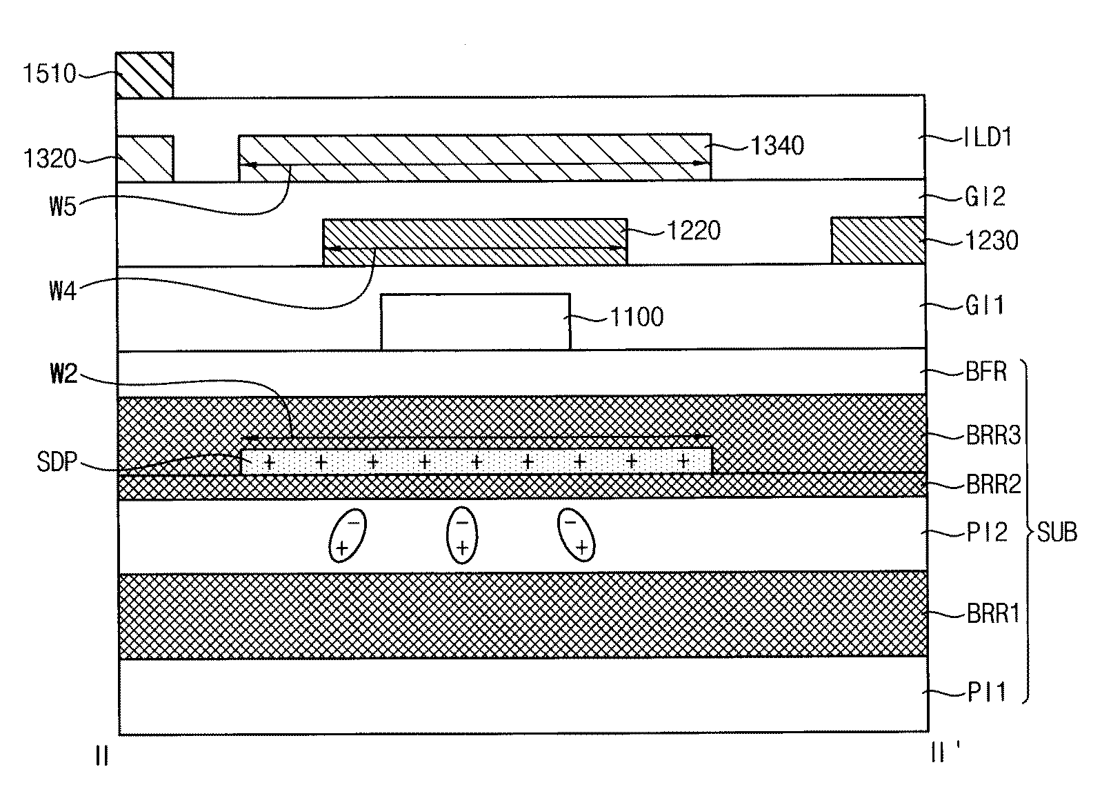
상기 표시 패널(100)은 상기 표시 영역(DA) 및 상기 지문 인식 영역(FA)과 중첩할 수 있다. 도 5에 도시된 바와 같이, 상기 표시 패널(100)은 회로 기판(110), 상기 회로 기판(110) 상에 배치되는 발광층(120), 및 상기 발광층(120) 상에 배치되는 박막 봉지층(TFE)을 포함할 수 있다. 상기 회로 기판(110)은 베이스 기판(SUB) 및 소자층(TRL)을 포함할 수 있고, 상기 발광층(120)은 제1 전극(ADE), 화소 정의막(PDL), 유기 발광층(EL) 및 제2 전극(CTE)을 포함할 수 있다. 상기 발광층(120)은 상기 회로 기판(110)으로부터 상기 구동 전류를 제공받아 광을 방출할 수 있다.The display panel (100) may overlap the display area (DA) and the fingerprint recognition area (FA). As illustrated in FIG. 5, the display panel (100) may include a circuit board (110), a light-emitting layer (120) disposed on the circuit board (110), and a thin film encapsulation layer (TFE) disposed on the light-emitting layer (120). The circuit board (110) may include a base substrate (SUB) and a device layer (TRL), and the light-emitting layer (120) may include a first electrode (ADE), a pixel defining layer (PDL), an organic light-emitting layer (EL), and a second electrode (CTE). The light-emitting layer (120) may receive the driving current from the circuit board (110) and emit light.
상기 보호 필름(PFL)은 상기 표시 패널(100)의 하부에 배치될 수 있다. 상기 보호 필름(PFL)은 상기 표시 영역(DA)과 중첩할 수 있으며, 상기 지문 인식 영역(FA)과 중첩하지 않을 수 있다. 다시 말하면, 상기 보호 필름(PFL)에는 상기 지문 인식 영역(FA)과 중첩하는 개구가 형성될 수 있다. 상기 보호 필름(PFL)은 플라스틱 물질을 포함할 수 있으며, 상기 표시 패널(100)을 지지할 수 있다.The protective film (PFL) may be disposed at a lower portion of the display panel (100). The protective film (PFL) may overlap the display area (DA) and may not overlap the fingerprint recognition area (FA). In other words, an opening may be formed in the protective film (PFL) that overlaps the fingerprint recognition area (FA). The protective film (PFL) may include a plastic material and may support the display panel (100).
상기 공기층(ARL)은 상기 표시 패널(100)의 하부에 배치될 수 있다. 상기 공기층(ARL)은 상기 지문 인식 영역(FA)과 중첩할 수 있으며, 상기 표시 영역(DA)과 중첩하지 않을 수 있다. 다시 말하면, 상기 공기층(ARL)은 상기 개구에 형성될 수 있다. 상기 공기층(ARL)에 의해 상기 광 센서 모듈(LSM)으로 광이 원활하게 투과될 수 있다.The air layer (ARL) may be arranged at the bottom of the display panel (100). The air layer (ARL) may overlap the fingerprint recognition area (FA) and may not overlap the display area (DA). In other words, the air layer (ARL) may be formed in the opening. Light may be smoothly transmitted to the light sensor module (LSM) by the air layer (ARL).
상기 쿠션층(CSL)은 상기 보호 필름(PFL)의 하부에 배치될 수 있다. 상기 쿠션층(CSL)은 상기 표시 영역(DA)과 중첩할 수 있으며, 상기 지문 인식 영역(FA)과 중첩하지 않을 수 있다. 다시 말하면, 상기 쿠션층(CSL)에는 상기 지문 인식 영역(FA)과 중첩하는 개구가 형성될 수 있다. 상기 쿠션층(CSL)은 탄성체를 포함할 수 있으며, 외부 충격으로부터 상기 표시 패널(100)을 보호할 수 있다.The cushion layer (CSL) may be arranged under the protective film (PFL). The cushion layer (CSL) may overlap the display area (DA) and may not overlap the fingerprint recognition area (FA). In other words, an opening may be formed in the cushion layer (CSL) that overlaps the fingerprint recognition area (FA). The cushion layer (CSL) may include an elastic body and may protect the display panel (100) from external impact.
상기 광 센서 모듈(LSM)은 상기 보호 필름(PFL)의 하부에 배치될 수 있다. 상기 광 센서 모듈(LSM)은 상기 지문 인식 영역(FA)과 중첩할 수 있다. 다시 말하면, 상기 광 센서 모듈(LSM)은 상기 쿠션층(CSL)에 형성되는 상기 개구에 배치될 수 있다. 상기 광 센서 모듈(LSM)은 사용자의 지문을 인식할 수 있다. 예를 들어, 상기 표시 패널(100)에서 방출된 광이 상기 사용자의 손가락에서 반사될 수 있고, 상기 광 센서 모듈(LSM)은 상기 손가락에서 반사된 광을 감지할 수 있다. 상기 광 센서 모듈(LSM)이 광을 감지하기 위해, 상기 광 센서 모듈(LSM)은 상기 공기층(ARL)에 의해 노출될 수 있다.The above-described light sensor module (LSM) may be disposed under the protective film (PFL). The light sensor module (LSM) may overlap the fingerprint recognition area (FA). In other words, the light sensor module (LSM) may be disposed in the opening formed in the cushion layer (CSL). The light sensor module (LSM) may recognize a user's fingerprint. For example, light emitted from the display panel (100) may be reflected from the user's finger, and the light sensor module (LSM) may detect the light reflected from the finger. In order for the light sensor module (LSM) to detect light, the light sensor module (LSM) may be exposed by the air layer (ARL).
상기 편광층(POL)은 상기 표시 패널(100)의 상부에 배치될 수 있다. 상기 편광층(POL)이 외광을 편광시킴에 따라, 상기 표시 패널(100)에서 방출되는 광이 사용자에게 명확하게 시인될 수 있다.The polarizing layer (POL) may be placed on the upper portion of the display panel (100). As the polarizing layer (POL) polarizes external light, light emitted from the display panel (100) may be clearly recognized by the user.
상기 윈도우(WIN)는 상기 편광층(POL)의 상부에 배치될 수 있다. 상기 윈도우(WIN)는 유리, 플라스틱 등으로 이루어질 수 있으며, 외부 충격으로부터 상기 표시 패널(100)을 보호할 수 있다.The above window (WIN) may be placed on the upper part of the polarizing layer (POL). The window (WIN) may be made of glass, plastic, or the like, and may protect the display panel (100) from external impact.
한편, 상기 공기층(ARL)이 상기 표시 패널(100)의 하부에 배치됨에 따라, 상기 지문 인식 영역(FA)과 중첩하는 상기 표시 패널(100)로 광이 입사될 수 있다. 예를 들어, 외부로부터 입사되어 상기 광 센서 모듈(LSM)에서 반사된 광(11) 및/또는 상기 표시 패널(100)에서 방출되어 상기 광 센서 모듈(LSM)에서 반사된 광(12)이 상기 표시 패널(100)로 입사될 수 있다.Meanwhile, as the air layer (ARL) is arranged at the bottom of the display panel (100), light may be incident on the display panel (100) overlapping the fingerprint recognition area (FA). For example, light (11) incident from the outside and reflected from the light sensor module (LSM) and/or light (12) emitted from the display panel (100) and reflected from the light sensor module (LSM) may be incident on the display panel (100).
상기 소자층(TRL)에는 상술한 트랜지스터들이 배치될 수 있고, 상기 소자층에 제공되는 신호 및 전압에 의해 상기 소자층(TRL)에서는 전기장이 발생할 수 있다. 상기 베이스 기판(SUB)은 유기 물질 등의 유전체를 포함할 수 있고, 상기 전기장에 의해 상기 유기 물질들이 분극될 수 있다. 상기 분극된 유기 물질들은 상기 소자층에 전기적인 영향을 미칠 수 있으며, 이는 표시 장치의 표시 품질을 저하시킬 수 있다. 또한, 상기 분극 현상은 상기 표시 패널(100)로 입사되는 광에 의해 더욱 가속화될 수 있다. 상기 표시 장치(10)는 상기 베이스 기판(SUB)의 내부에 차폐 패턴(예를 들어, 도 8, 21 및 22의 SDP)을 포함함으로써, 상기 분극 현상이 상기 소자층에 전기적인 영향을 미치지 않도록 할 수 있다. 그에 따라, 상기 표시 장치(10)는 표시 품질이 향상될 수 있다. 이에 대한 자세한 설명은 도 21 및 22를 참조하여 하기로 한다.The above-described transistors may be arranged on the above-described element layer (TRL), and an electric field may be generated in the element layer (TRL) by a signal and voltage provided to the element layer. The base substrate (SUB) may include a dielectric such as an organic material, and the organic materials may be polarized by the electric field. The polarized organic materials may have an electrical effect on the element layer, which may deteriorate the display quality of the display device. In addition, the polarization phenomenon may be further accelerated by light incident on the display panel (100). The display device (10) may prevent the polarization phenomenon from having an electrical effect on the element layer by including a shielding pattern (for example, the SDP of FIGS. 8, 21, and 22) inside the base substrate (SUB). Accordingly, the display quality of the display device (10) may be improved. A detailed description thereof will be given with reference to FIGS. 21 and 22.
도 6 내지 도 20은 도 5의 표시 패널을 설명하기 위한 레이아웃 도면들이다.Figures 6 to 20 are layout drawings for explaining the display panel of Figure 5.
도 6을 참조하면, 상기 표시 패널(100)은 상기 화소 구조물(PX) 및 상기 화소 구조물(PX)과 인접하는 대칭 화소 구조물(PX1)을 포함할 수 있다. 예를 들어, 상기 대칭 화소 구조물(PX1)의 구조는 상기 화소 구조물(PX)의 구조를 가상의 대칭 라인(SL)을 기준으로 대칭시킨 구조와 실질적으로 동일할 수 있다. 이하에서는, 설명의 편의를 위해 상기 화소 구조물(PX)에 대하여 설명하기로 한다.Referring to FIG. 6, the display panel (100) may include the pixel structure (PX) and a symmetrical pixel structure (PX1) adjacent to the pixel structure (PX). For example, the structure of the symmetrical pixel structure (PX1) may be substantially the same as a structure in which the structure of the pixel structure (PX) is symmetrical with respect to a virtual symmetrical line (SL). Hereinafter, for convenience of explanation, the pixel structure (PX) will be described.
도 3, 4, 5, 6 및 7을 참조하면, 상기 화소 구조물(PX)은 상기 베이스 기판(SUB) 및 상기 베이스 기판(SUB) 상에 배치되는 차폐 패턴(SDP)을 포함할 수 있다. Referring to FIGS. 3, 4, 5, 6 and 7, the pixel structure (PX) may include the base substrate (SUB) and a shielding pattern (SDP) disposed on the base substrate (SUB).
상기 베이스 기판(SUB)은 유리 기판, 석영 기판, 플라스틱 기판 등을 포함할 수 있다. 일 실시예에서, 상기 베이스 기판(SUB)은 플라스틱 기판을 포함할 수 있고, 이에 따라 상기 표시 장치(10)는 플렉서블한 특성을 가질 수 있다. 이 경우, 상기 베이스 기판(SUB)은 적어도 하나의 유기 필름층 및 적어도 하나의 배리어층이 번갈아 가며 적층된 구조를 가질 수 있다. 예를 들면, 상기 유기 필름층은 폴리이미드와 같은 유기 물질을 사용하여 형성될 수 있고, 상기 배리어층은 무기 물질을 사용하여 형성될 수 있다. The base substrate (SUB) may include a glass substrate, a quartz substrate, a plastic substrate, etc. In one embodiment, the base substrate (SUB) may include a plastic substrate, and thus the display device (10) may have a flexible characteristic. In this case, the base substrate (SUB) may have a structure in which at least one organic film layer and at least one barrier layer are alternately laminated. For example, the organic film layer may be formed using an organic material such as polyimide, and the barrier layer may be formed using an inorganic material.
상기 차폐 패턴(SDP)은 상기 베이스 기판(SUB)의 내부에 배치될 수 있다. 예를 들어, 상기 베이스 기판(SUB)은 상기 배리어층을 포함할 수 있고, 상기 차폐 패턴(SDP)은 상기 배리어층의 내부에 배치될 수 있다. 예를 들어, 상기 유기 필름층 상에 제1 배리어층을 형성한 후, 상기 제1 배리어층 상에 상기 차폐 패턴(SDP)을 형성하고, 상기 제1 배리어층 상에 상기 차폐 패턴(SDP)을 커버하도록 제2 배리어층을 형성할 수 있다. 상기 차폐 패턴(SDP)은 상기 제1 및 제2 배리어층들 사이에 배치됨으로써, 상기 베이스 기판(SUB)의 내부에 배치될 수 있다.The shielding pattern (SDP) may be arranged inside the base substrate (SUB). For example, the base substrate (SUB) may include the barrier layer, and the shielding pattern (SDP) may be arranged inside the barrier layer. For example, after forming a first barrier layer on the organic film layer, the shielding pattern (SDP) may be formed on the first barrier layer, and a second barrier layer may be formed on the first barrier layer to cover the shielding pattern (SDP). The shielding pattern (SDP) may be arranged between the first and second barrier layers, and thus may be arranged inside the base substrate (SUB).
일 실시예에서, 상기 차폐 패턴(SDP)은 실리콘 반도체를 포함할 수 있다. 예를 들어, 상기 차폐 패턴(SDP)은 비정질 실리콘(amorphous silicon) 또는 다결정 실리콘(polycrystalline silicon)을 포함할 수 있다. 또한, 상기 차폐 패턴(SDP)에는 양이온 또는 음이온이 도핑될 수 있다. 예를 들어, 상기 양이온은 III족 원소일 수 있으며, 붕소(boron) 등일 수 있다. 상기 음이온은 V족 원소일 수 있으며, 인(phosphorus) 등일 수 있다.In one embodiment, the shielding pattern (SDP) may include a silicon semiconductor. For example, the shielding pattern (SDP) may include amorphous silicon or polycrystalline silicon. In addition, the shielding pattern (SDP) may be doped with a cation or anion. For example, the cation may be a group III element, such as boron. The anion may be a group V element, such as phosphorus.
일 실시예에서, 상기 차폐 패턴(SDP)은 후술할 게이트 전극(예를 들어, 도 9의 1220)과 완전히 중첩할 수 있다. 다시 말하면, 상기 차폐 패턴(SDP)의 형상은 상기 게이트 전극(1220)의 형상과 실질적으로 동일할 수 있고, 상기 차폐 패턴(SDP)의 크기는 상기 게이트 전극(1220)의 크기보다 크거나 같을 수 있다.In one embodiment, the shielding pattern (SDP) may completely overlap with a gate electrode (e.g., 1220 of FIG. 9) to be described later. In other words, the shape of the shielding pattern (SDP) may be substantially the same as the shape of the gate electrode (1220), and the size of the shielding pattern (SDP) may be larger than or equal to the size of the gate electrode (1220).
일 실시예에서, 도 7에 도시된 바와 같이, 상기 차폐 패턴(SDP)은 오각형 형상일 수 있고, 상기 제1 방향(D1)으로의 제1 폭(W1) 및 상기 제2 방향(D2)으로의 제2 폭(W2)을 가질 수 있다. 또한, 상기 게이트 전극(1220)은 상기 오각형 형상일 수 있고, 상기 제1 방향(D1)으로의 제3 폭(W3) 및 상기 제2 방향(D2)으로의 제4 폭(W4)을 가질 수 있다. 상기 제1 폭(W1)은 상기 제3 폭(W3)보다 대략 0.8um 내지 대략 1.2um 만큼 클 수 있고, 상기 제2 폭(W2)은 상기 제4 폭(W4)보다 대략 0.8um 내지 대략 1.2um 만큼 클 수 있다. In one embodiment, as illustrated in FIG. 7, the shielding pattern (SDP) may have a pentagonal shape and may have a first width (W1) in the first direction (D1) and a second width (W2) in the second direction (D2). In addition, the gate electrode (1220) may have the pentagonal shape and may have a third width (W3) in the first direction (D1) and a fourth width (W4) in the second direction (D2). The first width (W1) may be about 0.8 um to about 1.2 um larger than the third width (W3), and the second width (W2) may be about 0.8 um to about 1.2 um larger than the fourth width (W4).
일 실시예에서, 상기 차폐 패턴(SDP)의 두께는 상기 차폐 패턴(SDP)에 도핑되는 상기 양이온 또는 상기 음이온의 도핑 농도에 따라 설정될 수 있다. 예를 들어, 상기 도핑 농도에 비해 상기 차폐 패턴(SDP)의 두께가 얇은 경우, 상기 양이온 또는 상기 음이온이 상기 베이스 기판(SUB)에도 도핑될 수 있다. 또는, 상기 도핑 농도에 비해 상기 차폐 패턴(SDP)의 두께가 두꺼운 경우, 상기 양이온 또는 상기 음이온이 상기 차폐 패턴(SDP)에 불충분하게 도핑될 수 있다. 일 실시예에서, 상기 차폐 패턴(SDP)에 대략 1012농도의 붕소가 도핑되는 경우, 상기 차폐 패턴(SDP)의 두께는 대략 500um 내지 대략 1500um 일 수 있다.In one embodiment, the thickness of the shielding pattern (SDP) may be set according to the doping concentration of the cation or the anion doped into the shielding pattern (SDP). For example, when the thickness of the shielding pattern (SDP) is thin compared to the doping concentration, the cation or the anion may also be doped into the base substrate (SUB). Alternatively, when the thickness of the shielding pattern (SDP) is thick compared to the doping concentration, the cation or the anion may be insufficiently doped into the shielding pattern (SDP). In one embodiment, when the shielding pattern (SDP) is doped with boron at a concentration of about 10<12> , the thickness of the shielding pattern (SDP) may be about 500 um to about 1500 um.
상기 베이스 기판(SUB) 상에는 버퍼층이 배치될 수 있다. 상기 버퍼층은 상기 베이스 기판(SUB)으로부터 금속 원자들이나 불순물들이 제1 액티브 패턴(예를 들어, 도 8의 1100)으로 확산되는 현상을 방지할 수 있다. 또한, 상기 버퍼층은 상기 제1 액티브 패턴(1100)을 형성하기 위한 결정화 공정 동안 열의 제공 속도를 조절하여 상기 제1 액티브 패턴(1100)을 균일하게 형성할 수 있다.A buffer layer may be arranged on the base substrate (SUB). The buffer layer may prevent metal atoms or impurities from diffusing from the base substrate (SUB) to the first active pattern (e.g., 1100 of FIG. 8). In addition, the buffer layer may control a heat supply speed during a crystallization process for forming the first active pattern (1100) to uniformly form the first active pattern (1100).
도 8을 참조하면, 상기 제1 액티브 패턴(1100)은 상기 버퍼층 상에 배치될 수 있다. 일 실시예에서, 상기 제1 액티브 패턴(1100)은 실리콘 반도체를 포함할 수 있다. 예를 들어, 상기 제1 액티브 패턴(1100)은 비정질 실리콘, 다결정 실리콘 등을 포함할 수 있다.Referring to FIG. 8, the first active pattern (1100) may be placed on the buffer layer. In one embodiment, the first active pattern (1100) may include a silicon semiconductor. For example, the first active pattern (1100) may include amorphous silicon, polycrystalline silicon, or the like.
일 실시예에서, 상기 제1 액티브 패턴(1100)에는 양이온 또는 음이온이 선택적으로 주입될 수 있다. 예를 들어, 상기 제1, 제2, 제5, 제6, 및 제7 트랜지스터들(T1, T2, T5, T6, T7)이 상기 피모스 트랜지스터들인 경우, 상기 제1 액티브 패턴(1100)은 상기 양이온이 주입되는 소스 영역, 상기 양이온이 주입되는 드레인 영역, 및 상기 양이온이 주입되지 않는 채널 영역을 포함할 수 있다.In one embodiment, the first active pattern (1100) may be selectively injected with positive or negative ions. For example, when the first, second, fifth, sixth, and seventh transistors (T1, T2, T5, T6, and T7) are PMOS transistors, the first active pattern (1100) may include a source region into which the positive ions are injected, a drain region into which the positive ions are injected, and a channel region into which the positive ions are not injected.
제1 게이트 절연층(예를 들어, 도 21의 GI1)은 상기 제1 액티브 패턴(1100)을 덮으며, 상기 버퍼층 상에 배치될 수 있다. 상기 제1 게이트 절연층은 절연 물질을 포함할 수 있다. 예를 들어, 상기 제1 게이트 절연층은 실리콘 산화물, 실리콘 질화물, 티타늄 산화물, 탄탈륨 산화물 등을 포함할 수 있다.A first gate insulating layer (e.g., GI1 of FIG. 21) covers the first active pattern (1100) and may be disposed on the buffer layer. The first gate insulating layer may include an insulating material. For example, the first gate insulating layer may include silicon oxide, silicon nitride, titanium oxide, tantalum oxide, or the like.
도 9 및 10을 참조하면, 제1 도전 패턴(1200)은 상기 제1 게이트 절연층 상에 배치될 수 있다. 상기 제1 도전 패턴(1200)은 제1 게이트 배선(1210), 게이트 전극(1220), 제2 게이트 배선(1230)을 포함할 수 있다.Referring to FIGS. 9 and 10, a first conductive pattern (1200) may be disposed on the first gate insulating layer. The first conductive pattern (1200) may include a first gate wiring (1210), a gate electrode (1220), and a second gate wiring (1230).
상기 제1 게이트 배선(1210)은 상기 제1 액티브 패턴(1100) 상에 배치되고, 상기 제1 방향(D1)으로 연장될 수 있다. 예를 들어, 상기 제1 게이트 배선(1210)은 상기 제1 액티브 패턴(1100)의 일부와 함께 상기 제2 트랜지스터(T2)를 구성할 수 있다. 상기 제1 게이트 배선(1210)에는 상기 제1 게이트 신호(GW)가 제공될 수 있다.The first gate wiring (1210) may be arranged on the first active pattern (1100) and may extend in the first direction (D1). For example, the first gate wiring (1210) may form the second transistor (T2) together with a part of the first active pattern (1100). The first gate signal (GW) may be provided to the first gate wiring (1210).
예를 들어, 상기 제1 게이트 배선(1210)은 상기 제1 액티브 패턴(1100)의 다른 일부와 함께 상기 제7 트랜지스터(T7)를 구성할 수 있다. 이를 위해, 상기 제1 게이트 배선(1210)에는 상기 제4 게이트 신호(GB)가 제공될 수 있다. 예를 들어, 상기 제1 게이트 신호(GW)와 상기 제4 게이트 신호(GB)는 시간차를 두고 실질적으로 동일한 파형을 가질 수 있다.For example, the first gate wiring (1210) may form the seventh transistor (T7) together with another part of the first active pattern (1100). To this end, the fourth gate signal (GB) may be provided to the first gate wiring (1210). For example, the first gate signal (GW) and the fourth gate signal (GB) may have substantially the same waveform with a time difference.
상기 게이트 전극(1220)은 상기 제1 액티브 패턴(1100)의 일부와 함께 상기 제1 트랜지스터(T1)를 구성할 수 있다.The above gate electrode (1220) can form the first transistor (T1) together with a part of the first active pattern (1100).
상기 제2 게이트 배선(1230)은 상기 제1 액티브 패턴(1100) 상에 배치되고, 상기 제1 방향(D1)으로 연장될 수 있다. 일 실시예에서, 상기 제2 게이트 배선(1230)은 평면 상에서 상기 게이트 전극의 일 측과 인접할 수 있다. 예를 들어, 상기 제2 게이트 배선(1230)은 상기 제1 액티브 패턴(1100)의 일부와 함께 상기 제5 및 제6 트랜지스터들(T5, T6)을 구성할 수 있다. 상기 제2 게이트 배선(1230)에는 상기 발광 제어 신호(EM)가 제공될 수 있다. 예를 들어, 상기 제2 게이트 배선(1230)은 발광 제어 배선으로 지칭될 수 있다.The second gate wiring (1230) may be arranged on the first active pattern (1100) and may extend in the first direction (D1). In one embodiment, the second gate wiring (1230) may be adjacent to one side of the gate electrode on a plane. For example, the second gate wiring (1230) may configure the fifth and sixth transistors (T5, T6) together with a part of the first active pattern (1100). The light emission control signal (EM) may be provided to the second gate wiring (1230). For example, the second gate wiring (1230) may be referred to as a light emission control wiring.
예를 들어, 상기 제1 도전 패턴(1200)은 금속, 합금, 도전 금속 산화물, 투명 도전 물질 등을 포함할 수 있다. 예를 들어, 상기 제1 도전 패턴(1200)은 은(Ag), 은을 함유하는 합금, 몰리브데늄(Mo), 몰리브데늄을 함유하는 합금, 알루미늄(Al), 알루미늄을 함유하는 합금, 알루미늄 질화물(AlN), 텅스텐(W), 텅스텐 질화물(WN), 구리(Cu), 니켈(Ni), 크롬(Cr), 크롬 질화물(CrN), 티타늄(Ti), 탄탈륨(Ta), 백금(Pt), 스칸듐(Sc), 인듐 주석 산화물(ITO), 인듐 아연 산화물(IZO) 등을 포함할 수 있다.For example, the first conductive pattern (1200) may include a metal, an alloy, a conductive metal oxide, a transparent conductive material, and the like. For example, the first conductive pattern (1200) may include silver (Ag), an alloy containing silver, molybdenum (Mo), an alloy containing molybdenum, aluminum (Al), an alloy containing aluminum, aluminum nitride (AlN), tungsten (W), tungsten nitride (WN), copper (Cu), nickel (Ni), chromium (Cr), chromium nitride (CrN), titanium (Ti), tantalum (Ta), platinum (Pt), scandium (Sc), indium tin oxide (ITO), indium zinc oxide (IZO), and the like.
제2 게이트 절연층(예를 들어, 도 21의 GI2)은 상기 제1 도전 패턴(1200)을 덮으며, 상기 제1 게이트 절연층 상에 배치될 수 있다. 상기 제2 게이트 절연층은 절연 물질을 포함할 수 있다.A second gate insulating layer (e.g., GI2 of FIG. 21) covers the first conductive pattern (1200) and may be disposed on the first gate insulating layer. The second gate insulating layer may include an insulating material.
한편, 상기 제1, 제2, 제5, 제6, 제7 트랜지스터들(T1, T2, T5, T6, T7)은 도 3을 참조하여 설명한 제1, 제2, 제5, 제6, 제7 트랜지스터들(T1, T2, T5, T6, T7)과 실질적으로 동일할 수 있다. 예를 들어, 상기 게이트 전극(1220)은 도 3을 참조하여 설명한 제1 트랜지스터(T1)의 게이트 단자에 대응할 수 있다. 다만 이러한 대응 관계에 대하여는 상세히 설명하지 않기로 하며, 상기 대응 관계는 본 발명이 속하는 기술분야의 통상의 기술자에게 자명할 것이다.Meanwhile, the first, second, fifth, sixth, and seventh transistors (T1, T2, T5, T6, and T7) may be substantially the same as the first, second, fifth, sixth, and seventh transistors (T1, T2, T5, T6, and T7) described with reference to FIG. 3. For example, the gate electrode (1220) may correspond to the gate terminal of the first transistor (T1) described with reference to FIG. 3. However, this correspondence will not be described in detail, and the correspondence will be apparent to those skilled in the art to which the present invention pertains.
도 11 및 12를 참조하면, 제2 도전 패턴(1300)은 상기 제2 게이트 절연층 상에 배치될 수 있다. 상기 제2 도전 패턴(1300)은 게이트 초기화 전압 배선(1310), 제3 게이트 배선(1320), 제4 게이트 배선(1330) 및 스토리지 커패시터 전극(1340)을 포함할 수 있다.Referring to FIGS. 11 and 12, a second conductive pattern (1300) may be disposed on the second gate insulating layer. The second conductive pattern (1300) may include a gate initialization voltage wiring (1310), a third gate wiring (1320), a fourth gate wiring (1330), and a storage capacitor electrode (1340).
상기 게이트 초기화 전압 배선(1310)은 상기 제1 방향(D1)으로 연장될 수 있다. 일 실시예에서, 상기 게이트 초기화 전압 배선(1310)은 상기 제4 트랜지스터(T4)로 상기 게이트 초기화 전압(VINT)을 제공할 수 있다. 예를 들어, 상기 게이트 초기화 전압 배선(1310)은 후술할 제2 액티브 패턴(예를 들어, 도 13의 1400)으로 상기 게이트 초기화 전압(VINT)을 제공할 수 있다.The gate initialization voltage wiring (1310) may extend in the first direction (D1). In one embodiment, the gate initialization voltage wiring (1310) may provide the gate initialization voltage (VINT) to the fourth transistor (T4). For example, the gate initialization voltage wiring (1310) may provide the gate initialization voltage (VINT) to a second active pattern (e.g., 1400 of FIG. 13) to be described later.
상기 제3 게이트 배선(1320)은 상기 제1 방향(D1)으로 연장될 수 있다. 일 실시예에서, 상기 제3 게이트 배선(1320)은 평면 상에서 상기 게이트 전극(1220)의 상기 일 측과 반대되는 타 측에 인접할 수 있다. 일 실시예에서, 상기 제3 게이트 배선(1320)은 상기 제3 트랜지스터(T3)로 상기 제2 게이트 신호(GC)를 제공할 수 있다. 예를 들어, 상기 제3 게이트 배선(1320)은 상기 제3 트랜지스터(T3)의 상기 하부 게이트 단자로 기능할 수 있다. 예를 들어, 상기 제3 게이트 배선(1320)은 하부 보상 제어 배선으로 지칭될 수 있다.The third gate wiring (1320) may extend in the first direction (D1). In one embodiment, the third gate wiring (1320) may be adjacent to the other side of the gate electrode (1220) opposite to the one side on a plane. In one embodiment, the third gate wiring (1320) may provide the second gate signal (GC) to the third transistor (T3). For example, the third gate wiring (1320) may function as the lower gate terminal of the third transistor (T3). For example, the third gate wiring (1320) may be referred to as a lower compensation control wiring.
상기 제4 게이트 배선(1330)은 상기 제1 방향(D1)으로 연장될 수 있다. 일 실시예에서, 상기 제4 게이트 배선(1330)은 상기 제4 트랜지스터(T4)로 상기 제3 게이트 신호(GI)를 제공할 수 있다. 예를 들어, 상기 제4 게이트 배선(1330)은 상기 제4 트랜지스터(T4)의 상기 하부 게이트 단자로 기능할 수 있다. The fourth gate wiring (1330) may extend in the first direction (D1). In one embodiment, the fourth gate wiring (1330) may provide the third gate signal (GI) to the fourth transistor (T4). For example, the fourth gate wiring (1330) may function as the lower gate terminal of the fourth transistor (T4).
상기 스토리지 커패시터 전극(1340)은 상기 제1 방향(D1)으로 연장될 수 있다. 일 실시예에서, 상기 스토리지 커패시터 전극(1340)은 상기 게이트 전극(1220)과 함께 상기 스토리지 커패시터(CST)를 구성할 수 있다. 예를 들어, 상기 스토리지 커패시터 전극(1340)은 상기 게이트 전극(1220)과 중첩할 수 있으며, 상기 스토리지 커패시터 전극(1340)에는 상기 고전원 전압(ELVDD)이 제공될 수 있다.The storage capacitor electrode (1340) may extend in the first direction (D1). In one embodiment, the storage capacitor electrode (1340) may form the storage capacitor (CST) together with the gate electrode (1220). For example, the storage capacitor electrode (1340) may overlap the gate electrode (1220), and the high power voltage (ELVDD) may be provided to the storage capacitor electrode (1340).
일 실시예에서, 상기 스토리지 커패시터 전극(1340)은 상기 게이트 전극(1220)의 상면을 노출시키는 개구(H)를 포함할 수 있다. 예를 들어, 상기 개구(H)를 통해, 상기 제1 트랜지스터(T1)의 게이트 단자는 상기 제3 트랜지스터(T3)의 제1 단자와 전기적으로 연결될 수 있다.In one embodiment, the storage capacitor electrode (1340) may include an opening (H) exposing an upper surface of the gate electrode (1220). For example, through the opening (H), the gate terminal of the first transistor (T1) may be electrically connected to the first terminal of the third transistor (T3).
일 실시예에서, 상기 스토리지 커패시터 전극(1340)은 상기 제2 방향(D2)으로의 제5 폭(W5)을 가질 수 있다. 상기 제5 폭(W5)은 상기 차폐 패턴(SDP)의 상기 제2 폭(W2)와 동일할 수 있다.In one embodiment, the storage capacitor electrode (1340) may have a fifth width (W5) in the second direction (D2). The fifth width (W5) may be equal to the second width (W2) of the shielding pattern (SDP).
예를 들어, 상기 제2 도전 패턴(1300)은 금속, 합금, 도전 금속 산화물, 투명 도전 물질 등을 포함할 수 있다.For example, the second challenge pattern (1300) may include a metal, an alloy, a challenge metal oxide, a transparent challenge material, etc.
제1 층간 절연층(예를 들어, 도 21의 ILD1)은 상기 제2 도전 패턴(1300)을 덮으며, 상기 제2 게이트 절연층 상에 배치될 수 있다. 상기 제1 층간 절연층은 절연 물질을 포함할 수 있다.A first interlayer insulating layer (e.g., ILD1 of FIG. 21) may cover the second conductive pattern (1300) and be disposed on the second gate insulating layer. The first interlayer insulating layer may include an insulating material.
도 13 및 14를 참조하면, 제2 액티브 패턴(1400)은 상기 제1 층간 절연층 상에 배치될 수 있다. 예를 들어, 상기 제2 액티브 패턴(1400)은 상기 제3 게이트 배선(1320) 및 상기 제4 게이트 배선(1340)과 중첩할 수 있다.Referring to FIGS. 13 and 14, the second active pattern (1400) may be disposed on the first interlayer insulating layer. For example, the second active pattern (1400) may overlap the third gate wiring (1320) and the fourth gate wiring (1340).
일 실시예에서, 상기 제2 액티브 패턴(1400)은 상기 제1 액티브 패턴(1100)과 서로 다른 층에 배치되고, 상기 제1 액티브 패턴(1100)과 중첩하지 않을 수 있다. 다시 말하면, 상기 제2 액티브 패턴(1400)은 상기 제1 액티브 패턴(1100)과 별도로 형성될 수 있다. 예를 들어, 상기 제1 액티브 패턴(1100)은 상기 실리콘 반도체를 포함하고, 상기 제2 액티브 패턴(1400)은 산화물 반도체를 포함할 수 있다.In one embodiment, the second active pattern (1400) may be arranged in a different layer from the first active pattern (1100) and may not overlap with the first active pattern (1100). In other words, the second active pattern (1400) may be formed separately from the first active pattern (1100). For example, the first active pattern (1100) may include the silicon semiconductor, and the second active pattern (1400) may include an oxide semiconductor.
일 실시예에서, 상기 화소 구조물(PX)은 실리콘계 반도체 소자인 상기 제1, 제2, 제5, 제6 및 제7 트랜지스터들(T1, T2, T5, T6, T7) 및 산화물계 반도체 소자인 상기 제3 및 제4 트랜지스터들(T3, T4)을 포함할 수 있다. 예를 들어, 상기 제1, 제2, 제5, 제6 및 제7 트랜지스터들(T1, T2, T5, T6, T7)은 상기 피모스 트랜지스터들이고, 상기 제3 및 제4 트랜지스터들(T3, T4)은 상기 엔모스 트랜지스터들일 수 있다.In one embodiment, the pixel structure (PX) may include the first, second, fifth, sixth and seventh transistors (T1, T2, T5, T6, T7) which are silicon-based semiconductor devices and the third and fourth transistors (T3, T4) which are oxide-based semiconductor devices. For example, the first, second, fifth, sixth and seventh transistors (T1, T2, T5, T6, T7) may be PMOS transistors, and the third and fourth transistors (T3, T4) may be NMOS transistors.
제3 게이트 절연층은 상기 제2 액티브 패턴(1400)을 덮으며, 상기 제1 층간 절연층 상에 배치될 수 있다. 상기 제3 게이트 절연층은 절연 물질을 포함할 수 있다.The third gate insulating layer covers the second active pattern (1400) and may be disposed on the first interlayer insulating layer. The third gate insulating layer may include an insulating material.
도 15 및 16을 참조하면, 제3 도전 패턴(1500)은 상기 제3 게이트 절연층 상에 배치될 수 있다. 상기 제3 도전 패턴(1500)은 제5 게이트 배선(1510) 및 제6 게이트 배선(1520)을 포함할 수 있다.Referring to FIGS. 15 and 16, a third conductive pattern (1500) may be disposed on the third gate insulating layer. The third conductive pattern (1500) may include a fifth gate wiring (1510) and a sixth gate wiring (1520).
상기 제5 게이트 배선(1510)은 상기 제1 방향(D1)으로 연장될 수 있다. 일 실시예에서, 상기 제5 게이트 배선(1510)은 상기 제3 게이트 배선(1320)과 중첩할 수 있다. 일 실시예에서, 상기 제5 게이트 배선(1510)은 상기 제3 트랜지스터(T3)로 상기 제2 게이트 신호(GC)를 제공할 수 있다. 예를 들어, 상기 제5 게이트 배선(1510)은 상기 제3 트랜지스터(T3)의 상기 상부 게이트 단자로 기능할 수 있다. 예를 들어, 상기 제5 게이트 배선(1510)은 상부 보상 제어 배선으로 지칭될 수 있다.The fifth gate wiring (1510) may extend in the first direction (D1). In one embodiment, the fifth gate wiring (1510) may overlap the third gate wiring (1320). In one embodiment, the fifth gate wiring (1510) may provide the second gate signal (GC) to the third transistor (T3). For example, the fifth gate wiring (1510) may function as the upper gate terminal of the third transistor (T3). For example, the fifth gate wiring (1510) may be referred to as an upper compensation control wiring.
상기 제6 게이트 배선(1520)은 상기 제1 방향(D1)으로 연장될 수 있다. 일 실시예에서, 상기 제6 게이트 배선(1520)은 상기 제4 게이트 배선(1330)과 중첩할 수 있다. 일 실시예에서, 상기 제6 게이트 배선(1520)은 상기 제4 트랜지스터(T3)로 상기 제3 게이트 신호(GI)를 제공할 수 있다. 예를 들어, 상기 제6 게이트 배선(1520)은 상기 제4 트랜지스터(T3)의 상기 상부 게이트 단자로 기능할 수 있다. The sixth gate wiring (1520) may extend in the first direction (D1). In one embodiment, the sixth gate wiring (1520) may overlap the fourth gate wiring (1330). In one embodiment, the sixth gate wiring (1520) may provide the third gate signal (GI) to the fourth transistor (T3). For example, the sixth gate wiring (1520) may function as the upper gate terminal of the fourth transistor (T3).
제2 층간 절연층은 상기 제3 도전 패턴(1500)을 덮으며, 상기 제3 게이트 절연층 상에 배치될 수 있다. 상기 제2 층간 절연층은 절연 물질을 포함할 수 있다.The second interlayer insulating layer covers the third conductive pattern (1500) and may be disposed on the third gate insulating layer. The second interlayer insulating layer may include an insulating material.
도 17 및 18을 참조하면, 제4 도전 패턴(1600)은 상기 제2 층간 절연층 상에 배치될 수 있다. 상기 제4 도전 패턴(1600)은 데이터 패드(1610), 애노드 초기화 전압 배선(1620), 게이트 초기화 전압 연결 패턴(1630), 고전원 전압 연결 패턴(1640), 제1 보상 연결 패턴(1650), 제1 애노드 패드(1660), 및 제2 보상 연결 패턴(1670)을 포함할 수 있다.Referring to FIGS. 17 and 18, a fourth conductive pattern (1600) may be disposed on the second interlayer insulating layer. The fourth conductive pattern (1600) may include a data pad (1610), an anode initialization voltage wiring (1620), a gate initialization voltage connection pattern (1630), a high power voltage connection pattern (1640), a first compensation connection pattern (1650), a first anode pad (1660), and a second compensation connection pattern (1670).
상기 데이터 패드(1610)는 상기 데이터 전압(DATA)을 상기 제1 액티브 패턴(1100)으로 제공할 수 있다. 이를 위해, 상기 데이터 패드(1610)는 상기 제1 액티브 패턴(1100) 및 후술할 데이터 배선과 접촉할 수 있다. 예를 들어, 상기 데이터 패드(1610)는 상기 제1 액티브 패턴(1100) 및 상기 데이터 배선과 중첩할 수 있다.The above data pad (1610) can provide the data voltage (DATA) to the first active pattern (1100). To this end, the data pad (1610) can be in contact with the first active pattern (1100) and a data wire to be described later. For example, the data pad (1610) can overlap the first active pattern (1100) and the data wire.
상기 애노드 초기화 전압 배선(1620)은 상기 제7 트랜지스터(T7)로 상기 애노드 초기화 전압(AINT)을 제공할 수 있다. 예를 들어, 상기 애노드 초기화 전압 배선(1620)은 상기 제1 액티브 패턴(1100)으로 상기 애노드 초기화 전압(AINT)을 제공할 수 있다. 이를 위해, 상기 애노드 초기화 전압 배선(1620)은 상기 제1 액티브 패턴(1100)과 접촉할 수 있다.The anode initialization voltage wiring (1620) can provide the anode initialization voltage (AINT) to the seventh transistor (T7). For example, the anode initialization voltage wiring (1620) can provide the anode initialization voltage (AINT) to the first active pattern (1100). For this purpose, the anode initialization voltage wiring (1620) can be in contact with the first active pattern (1100).
상기 게이트 초기화 전압 연결 패턴(1630)은 상기 제4 트랜지스터(T4)로 상기 게이트 초기화 전압(VINT)을 제공할 수 있다. 예를 들어, 상기 게이트 초기화 전압 연결 패턴(1630)은 상기 제2 액티브 패턴(1400)으로 상기 게이트 초기화 전압(VINT)을 제공할 수 있다. 이를 위해, 상기 게이트 초기화 전압 연결 패턴(1630)은 상기 게이트 초기화 전압 배선(1310) 및 상기 제2 액티브 패턴(1400)과 접촉할 수 있다.The gate initialization voltage connection pattern (1630) can provide the gate initialization voltage (VINT) to the fourth transistor (T4). For example, the gate initialization voltage connection pattern (1630) can provide the gate initialization voltage (VINT) to the second active pattern (1400). To this end, the gate initialization voltage connection pattern (1630) can be in contact with the gate initialization voltage wiring (1310) and the second active pattern (1400).
상기 고전원 전압 연결 패턴(1640)은 상기 고전원 전압(EVLDD)을 상기 제1 액티브 패턴(1100)에 제공할 수 있다. 일 실시예에서, 상기 고전원 전압 연결 패턴(1640)은 후술할 고전원 전압 배선과 상기 제1 액티브 패턴(1100)을 전기적으로 연결시킬 수 있다. 예를 들어, 상기 고전원 전압 연결 패턴(1640)은 상기 고전원 전압 배선 및 상기 제1 액티브 패턴(1100)과 접촉할 수 있다.The high power voltage connection pattern (1640) can provide the high power voltage (EVLDD) to the first active pattern (1100). In one embodiment, the high power voltage connection pattern (1640) can electrically connect the high power voltage wiring, which will be described later, and the first active pattern (1100). For example, the high power voltage connection pattern (1640) can be in contact with the high power voltage wiring and the first active pattern (1100).
상기 제1 보상 연결 패턴(1650)은 상기 제1 트랜지스터(T1)의 게이트 단자와 상기 제3 트랜지스터(T3)의 제1 단자를 전기적으로 연결시킬 수 있다. 예를 들어, 상기 제1 보상 연결 패턴(1660)은 상기 제2 액티브 패턴(1400) 및 상기 게이트 전극(1220)과 접촉할 수 있다.The first compensation connection pattern (1650) can electrically connect the gate terminal of the first transistor (T1) and the first terminal of the third transistor (T3). For example, the first compensation connection pattern (1660) can be in contact with the second active pattern (1400) and the gate electrode (1220).
상기 제1 애노드 패드(1660)는 상기 유기 발광 다이오드의 상기 제1 단자로 상기 애노드 초기화 전압(AINT) 또는 상기 구동 전류를 제공할 수 있다. 예를 들어, 상기 제1 애노드 패드(1660)는 상기 제1 액티브 패턴(1100) 및 제2 애노드 패드(예를 들어, 도 19의 1730)와 접촉할 수 있다. The first anode pad (1660) can provide the anode initialization voltage (AINT) or the driving current to the first terminal of the organic light-emitting diode. For example, the first anode pad (1660) can be in contact with the first active pattern (1100) and the second anode pad (e.g., 1730 of FIG. 19).
제1 비아 절연층은 상기 제4 도전 패턴(1600)을 덮으며, 상기 제2 층간 절연층 상에 배치될 수 있다. 상기 제1 비아 절연층은 유기 절연 물질을 포함할 수 있다. 예를 들어, 상기 제1 비아 절연층은 포토레지스트, 폴리아크릴계 수지, 폴리이미드계 수지, 아크릴계 수지 등을 포함할 수 있다.The first via insulating layer covers the fourth conductive pattern (1600) and may be disposed on the second interlayer insulating layer. The first via insulating layer may include an organic insulating material. For example, the first via insulating layer may include photoresist, a polyacrylic resin, a polyimide resin, an acrylic resin, or the like.
도 19 및 20을 참조하면, 제5 도전 패턴(1700)은 상기 제1 비아 절연층 상에 배치될 수 있다. 상기 제5 도전 패턴(1700)은 데이터 배선(1710), 고전원 전압 배선(1720), 및 제2 애노드 패드(1730)를 포함할 수 있다.Referring to FIGS. 19 and 20, a fifth conductive pattern (1700) may be disposed on the first via insulating layer. The fifth conductive pattern (1700) may include a data wiring (1710), a high power voltage wiring (1720), and a second anode pad (1730).
상기 데이터 배선(1710)은 상기 제2 방향(D2)으로 연장할 수 있다. 일 실시예에서, 상기 데이터 배선(1710)은 상기 데이터 전압(DATA)을 상기 제2 트랜지스터(T2)로 제공할 수 있다. 이를 위해, 상기 데이터 배선(1710)은 상기 데이터 패드(1610)와 접촉할 수 있다.The above data wiring (1710) can extend in the second direction (D2). In one embodiment, the data wiring (1710) can provide the data voltage (DATA) to the second transistor (T2). To this end, the data wiring (1710) can be in contact with the data pad (1610).
상기 고전원 전압 배선(1720)은 상기 제2 방향(D2)으로 연장할 수 있다. 일 실시예에서, 상기 고전원 전압 배선(1720)은 상기 고전원 전압 연결 패턴(1640)으로 상기 고전원 전압(ELVDD)을 제공할 수 있다. 예를 들어, 상기 고전원 전압 배선(1720)은 상기 고전원 전압 연결 패턴(1640)과 접촉할 수 있다.The high power voltage wiring (1720) may extend in the second direction (D2). In one embodiment, the high power voltage wiring (1720) may provide the high power voltage (ELVDD) to the high power voltage connection pattern (1640). For example, the high power voltage wiring (1720) may be in contact with the high power voltage connection pattern (1640).
일 실시예에서, 상기 고전원 전압 배선(1720)은 상기 제2 액티브 패턴(1400)과 중첩할 수 있다. 예를 들어, 상기 제2 액티브 패턴(1400)은 산화물 반도체를 포함할 수 있다. 상기 산화물 반도체가 광에 노출되면, 상기 산화물 반도체를 포함하는 상기 제3 및 제4 트랜지스터들(T3, T4)을 통해 누설 전류가 발생될 수 있다. 예를 들어, 상기 광은 외광 또는 상기 유기 발광 다이오드(OLED)가 생성하는 광일 수 있다. 그러나, 상기 고전원 전압 패선(1720)이 상기 제2 액티브 패턴(1400)과 중첩함으로써, 상기 제2 액티브 패턴(1400)은 상기 광에 노출되지 않을 수 있다.In one embodiment, the high power voltage wiring (1720) may overlap the second active pattern (1400). For example, the second active pattern (1400) may include an oxide semiconductor. When the oxide semiconductor is exposed to light, a leakage current may be generated through the third and fourth transistors (T3, T4) including the oxide semiconductor. For example, the light may be external light or light generated by the organic light emitting diode (OLED). However, since the high power voltage wiring (1720) overlaps the second active pattern (1400), the second active pattern (1400) may not be exposed to the light.
상기 제2 애노드 패드(1730)는 상기 유기 발광 다이오드의 상기 제1 단자로 상기 애노드 초기화 전압(AINT) 또는 상기 구동 전류를 제공할 수 있다. 예를 들어, 상기 제2 애노드 패드(1730)는 상기 제1 애노드 패드(1660) 및 상기 제1 전극(예를 들어, 도 5의 ADE)과 접촉할 수 있다.The second anode pad (1730) can provide the anode initialization voltage (AINT) or the driving current to the first terminal of the organic light-emitting diode. For example, the second anode pad (1730) can be in contact with the first anode pad (1660) and the first electrode (e.g., ADE of FIG. 5).
제2 비아 절연층은 상기 제5 도전 패턴(1700)을 덮으며, 상기 제1 비아 절연층 상에 배치될 수 있다. 상기 제2 비아 절연층은 유기 절연 물질을 포함할 수 있다. 예를 들어, 상기 제2 비아 절연층은 포토레지스트, 폴리아크릴계 수지, 폴리이미드계 수지, 아크릴계 수지 등을 포함할 수 있다.The second via insulating layer covers the fifth conductive pattern (1700) and may be disposed on the first via insulating layer. The second via insulating layer may include an organic insulating material. For example, the second via insulating layer may include photoresist, a polyacrylic resin, a polyimide resin, an acrylic resin, or the like.
도 5를 참조하여 설명한 상기 발광층(120)은 상기 제2 비아 절연층 상에 배치될 수 있다. The light-emitting layer (120) described with reference to FIG. 5 may be placed on the second via insulating layer.
도 21은 도 16의 표시 패널을 II-II'선을 따라 절단한 일 예를 나타내는 단면도이다.Fig. 21 is a cross-sectional view showing an example of the display panel of Fig. 16 cut along line II-II'.
도 16 및 21을 참조하면, 상기 표시 패널(100)은 상기 베이스 기판(SUB), 상기 차폐 패턴(SDP), 상기 버퍼층(BFR), 상기 제1 액티브 패턴(1100), 상기 제1 게이트 절연층(GI1), 상기 게이트 전극(1220), 상기 제2 게이트 배선(1230), 상기 제2 게이트 절연층(GI2), 상기 제3 게이트 배선(1320), 상기 스토리지 커패시터 전극(1340), 상기 제1 층간 절연층(ILD1), 및 상기 제5 게이트 배선(1510)을 포함할 수 있다. Referring to FIGS. 16 and 21, the display panel (100) may include the base substrate (SUB), the shielding pattern (SDP), the buffer layer (BFR), the first active pattern (1100), the first gate insulating layer (GI1), the gate electrode (1220), the second gate wiring (1230), the second gate insulating layer (GI2), the third gate wiring (1320), the storage capacitor electrode (1340), the first interlayer insulating layer (ILD1), and the fifth gate wiring (1510).
상기 베이스 기판(SUB)은 제1 유기 필름층(PI1), 제1 배리어층(BRR1), 제2 유기 필름층(PI2), 제2 배리어층(BRR2), 및 제3 배리어층(BRR3)을 포함할 수 있다.The above base substrate (SUB) may include a first organic film layer (PI1), a first barrier layer (BRR1), a second organic film layer (PI2), a second barrier layer (BRR2), and a third barrier layer (BRR3).
상기 제1 및 제2 유기 필름층들(PI1, PI2)은 유기 물질을 포함할 수 있다. 예를 들어, 상기 제1 및 제2 유기 필름층들(PI1, PI2)은 폴리이미드를 포함할 수 있다. 상기 제1, 제2 및 제3 배리어층들(BRR1, BRR2, BRR3)은 무기 물질을 포함할 수 있다. 예를 들어, 상기 제1, 제2 및 제3 배리어층들(BRR1, BRR2, BRR3)은 실리콘 산화물을 포함할 수 있다.The first and second organic film layers (PI1, PI2) may include an organic material. For example, the first and second organic film layers (PI1, PI2) may include polyimide. The first, second and third barrier layers (BRR1, BRR2, BRR3) may include an inorganic material. For example, the first, second and third barrier layers (BRR1, BRR2, BRR3) may include silicon oxide.
일 실시예에서, 상기 제2 배리어층(BRR2)의 두께는 상기 제3 배리어층(BRR3)의 두께보다 작을 수 있다. 예를 들어, 상기 제2 배리어층(BRR2)의 두께는 대략 500um 이고, 상기 제3 배리어층(BRR3)의 두께는 대략 4500um 일 수 있다.In one embodiment, the thickness of the second barrier layer (BRR2) may be smaller than the thickness of the third barrier layer (BRR3). For example, the thickness of the second barrier layer (BRR2) may be approximately 500 um, and the thickness of the third barrier layer (BRR3) may be approximately 4500 um.
상기 차폐 패턴(SDP)은 상기 제2 배리어층(BRR2) 상에 배치될 수 있다. 상기 제3 배리어층(BRR3)은 상기 차폐 패턴(SDP)을 커버하며 상기 제2 배리어층(BRR2) 상에 배치될 수 있다. 상기 제2 배리어층(BRR2)의 두께가 상기 제3 배리어층(BRR3)의 두께보다 작으므로, 상기 차폐 패턴(SDP)은 상기 게이트 전극(1220)과 상대적으로 멀어질 수 있다. 그에 따라, 상기 차폐 패턴(SDP)과 상기 게이트 전극(1220) 사이의 커플링 현상을 방지할 수 있다. 또한, 상기 제2 배리어층(BRR2)이 일정한 두께를 가짐으로써, 상기 제2 배리어층(BRR2)은 상기 차폐 패턴(SDP)을 형성하는 과정에서 손상될 수 있는 상기 제2 유기 필름층(PI2)을 보호할 수 있다.The shielding pattern (SDP) may be disposed on the second barrier layer (BRR2). The third barrier layer (BRR3) may cover the shielding pattern (SDP) and be disposed on the second barrier layer (BRR2). Since the thickness of the second barrier layer (BRR2) is smaller than the thickness of the third barrier layer (BRR3), the shielding pattern (SDP) may be relatively far from the gate electrode (1220). Accordingly, a coupling phenomenon between the shielding pattern (SDP) and the gate electrode (1220) may be prevented. In addition, since the second barrier layer (BRR2) has a constant thickness, the second barrier layer (BRR2) may protect the second organic film layer (PI2) that may be damaged during the process of forming the shielding pattern (SDP).
상기 차폐 패턴(SDP)은 비정질 실리콘을 포함할 수 있다. 일 실시예에서, 상기 차폐 패턴(SDP)에는 양이온이 도핑될 수 있다. 다른 실시예에서, 상기 차폐 패턴(SDP)에는 정전압이 제공될 수 있다. 또 다른 실시예에서, 상기 차폐 패턴(SDP)에는 상기 발광 제어 신호(EM) 또는 상기 제2 게이트 신호(GC)가 제공될 수 있다.The shielding pattern (SDP) may include amorphous silicon. In one embodiment, the shielding pattern (SDP) may be doped with cations. In another embodiment, a positive voltage may be provided to the shielding pattern (SDP). In yet another embodiment, the light emission control signal (EM) or the second gate signal (GC) may be provided to the shielding pattern (SDP).
상술한 바와 같이, 상기 제2 게이트 배선(1230)에는 상기 발광 제어 신호(EM)가 제공될 수 있고, 상기 제3 게이트 배선(1320) 및 상기 제5 게이트 배선(1510)에는 상기 제2 게이트 신호(GC)가 제공될 수 있다. 상기 제5 및 제6 트랜지스터들(T5, T6)을 턴온시키기 위해, 상기 발광 제어 신호(EM)는 음의 전압 레벨을 가질 수 있다. 이와 동시에, 상기 제3 트랜지스터(T3)를 턴오프시키기 위해, 상기 제2 게이트 신호(GC)는 음의 전압 레벨을 가질 수 있다. 상기 발광 제어 신호(EM)와 상기 제2 게이트 신호(GC)가 동일한 음의 전압 레벨을 가짐으로써, 상기 제2 유기 필름층(PI2)에는 전기장이 형성될 수 있다. 그에 따라, 상기 제2 유기 필름층(PI2)의 유기 물질들이 분극될 수 있다. 분극된 상기 유기 물질들에 의해, 상기 제1 액티브 패턴(1100)에는 백채널(back channel)이 형성될 수 있다. 상기 백채널에 의해, 상기 제1 트랜지스터(T1)의 전기적 특성(예를 들어, 문턱 전압, 전자 이동도 등)이 변경될 수 있다. 그에 따라, 전기적 특성이 변경된 상기 제1 트랜지스터(T1)를 포함하는 상기 화소 구조물(PX)은 상기 데이터 전압(DATA)에 상응하지 않는 휘도를 발광할 수 있고, 표시 장치의 표시 품질이 저하될 수 있다.As described above, the light emission control signal (EM) may be provided to the second gate wiring (1230), and the second gate signal (GC) may be provided to the third gate wiring (1320) and the fifth gate wiring (1510). In order to turn on the fifth and sixth transistors (T5, T6), the light emission control signal (EM) may have a negative voltage level. At the same time, in order to turn off the third transistor (T3), the second gate signal (GC) may have a negative voltage level. Since the light emission control signal (EM) and the second gate signal (GC) have the same negative voltage level, an electric field may be formed in the second organic film layer (PI2). Accordingly, organic materials of the second organic film layer (PI2) may be polarized. By the polarized organic materials, a back channel may be formed in the first active pattern (1100). By the back channel, the electrical characteristics (e.g., threshold voltage, electron mobility, etc.) of the first transistor (T1) may be changed. Accordingly, the pixel structure (PX) including the first transistor (T1) with the changed electrical characteristics may emit light with a brightness that does not correspond to the data voltage (DATA), and the display quality of the display device may be degraded.
그러나, 본 발명의 일 실시예에 따른 상기 표시 장치(10)는 상기 베이스 기판(SUB)의 내부에 배치되는 상기 차폐 패턴(SDP)을 포함할 수 있다. 상기 차폐 패턴(SDP)은 분극된 상기 유기 물질들과 상기 제1 액티브 패턴(1100)을 차폐할 수 있다. 그에 따라, 상기 제1 액티브 패턴(1100)에는 상기 백채널이 형성되지 않을 수 있고, 상기 제1 트랜지스터(T1)의 전기적 특성이 변경되지 않을 수 있다. 따라서, 상기 표시 장치(10)의 표시 품질이 향상될 수 있다. However, the display device (10) according to one embodiment of the present invention may include the shielding pattern (SDP) arranged inside the base substrate (SUB). The shielding pattern (SDP) may shield the polarized organic materials and the first active pattern (1100). Accordingly, the back channel may not be formed in the first active pattern (1100), and the electrical characteristics of the first transistor (T1) may not be changed. Accordingly, the display quality of the display device (10) may be improved.
특히, 상기 유기 물질들의 분극 현상은 도 4를 참조하여 설명한 상기 표시 패널(100)로 입사되는 광(예를 들어, 도 4의 11 또는 12)에 의해 더욱 가속화될 수 있다. 그에 따라, 일 실시예에서, 상기 차폐 패턴(SDP)은 상기 지문 인식 영역(FA)과 중첩하고, 상기 표시 영역(DA)과 중첩하지 않을 수 있다. 다시 말하면, 상기 차폐 패턴(SDP)은 상기 지문 인식 영역(FA)과 중첩하는 상기 표시 패널(100)에만 형성되고, 상기 표시 영역(DA)과 중첩하는 상기 표시 패널(100)에는 형성되지 않을 수 있다. 물론, 다른 실시예에서, 상기 차폐 패턴(SDP)은 상기 지문 인식 영역(FA) 및 상기 표시 영역(DA)과 중첩하는 상기 표시 패널(100)에 형성될 수 있다. In particular, the polarization phenomenon of the organic materials may be further accelerated by light (for example, 11 or 12 of FIG. 4) incident on the display panel (100) described with reference to FIG. 4. Accordingly, in one embodiment, the shielding pattern (SDP) may overlap the fingerprint recognition area (FA) and may not overlap the display area (DA). In other words, the shielding pattern (SDP) may be formed only on the display panel (100) overlapping the fingerprint recognition area (FA), and may not be formed on the display panel (100) overlapping the display area (DA). Of course, in another embodiment, the shielding pattern (SDP) may be formed on the display panel (100) overlapping the fingerprint recognition area (FA) and the display area (DA).
도 22는 도 16의 표시 패널을 II-II'선을 따라 절단한 다른 예를 나타내는 단면도이다.Fig. 22 is a cross-sectional view showing another example of the display panel of Fig. 16 cut along line II-II'.
도 16 및 22를 참조하면, 상기 표시 패널(100)은 상기 베이스 기판(SUB), 상기 차폐 패턴(SDP'), 상기 버퍼층(BFR), 상기 제1 액티브 패턴(1100), 상기 제1 게이트 절연층(GI1), 상기 게이트 전극(1220), 상기 제2 게이트 배선(1230), 상기 제2 게이트 절연층(GI2), 상기 제3 게이트 배선(1320), 상기 스토리지 커패시터 전극(1340), 상기 제1 층간 절연층(ILD1), 및 상기 제5 게이트 배선(1510)을 포함할 수 있다. 다만, 상기 차폐 패턴(SDP')을 제외한 나머지 구성들은 도 21을 참조하여 설명하였으므로, 이하에서는 상기 차폐 패턴(SDP')에 대하여만 설명하기로 한다.Referring to FIGS. 16 and 22, the display panel (100) may include the base substrate (SUB), the shielding pattern (SDP'), the buffer layer (BFR), the first active pattern (1100), the first gate insulating layer (GI1), the gate electrode (1220), the second gate wiring (1230), the second gate insulating layer (GI2), the third gate wiring (1320), the storage capacitor electrode (1340), the first interlayer insulating layer (ILD1), and the fifth gate wiring (1510). However, since the remaining components except for the shielding pattern (SDP') have been described with reference to FIG. 21, only the shielding pattern (SDP') will be described below.
상기 차폐 패턴(SDP')은 비정질 실리콘을 포함할 수 있다. 일 실시예에서, 상기 차폐 패턴(SDP')에는 음이온이 도핑될 수 있다. 다른 실시예에서, 상기 차폐 패턴(SDP')에는 정전압이 제공될 수 있다. 또 다른 실시예에서, 상기 차폐 패턴(SDP')에는 상기 발광 제어 신호(EM) 또는 상기 제2 게이트 신호(GC)가 제공될 수 있다.The shielding pattern (SDP') may include amorphous silicon. In one embodiment, the shielding pattern (SDP') may be doped with an anion. In another embodiment, a positive voltage may be provided to the shielding pattern (SDP'). In yet another embodiment, the light emission control signal (EM) or the second gate signal (GC) may be provided to the shielding pattern (SDP').
본 발명의 일 실시예에 따른 상기 표시 장치(10)는 상기 베이스 기판(SUB)의 내부에 배치되는 상기 차폐 패턴(SDP')을 포함할 수 있다. 상기 차폐 패턴(SDP')은 분극된 상기 유기 물질들과 상기 제1 액티브 패턴(1100)을 차폐할 수 있다. 그에 따라, 상기 제1 액티브 패턴(1100)에는 상기 백채널이 형성되지 않을 수 있고, 상기 제1 트랜지스터(T1)의 전기적 특성이 변경되지 않을 수 있다. 따라서, 상기 표시 장치(10)의 표시 품질이 향상될 수 있다. The display device (10) according to one embodiment of the present invention may include the shielding pattern (SDP') arranged inside the base substrate (SUB). The shielding pattern (SDP') may shield the polarized organic materials and the first active pattern (1100). Accordingly, the back channel may not be formed in the first active pattern (1100), and the electrical characteristics of the first transistor (T1) may not be changed. Accordingly, the display quality of the display device (10) may be improved.
상술한 바에서는, 본 발명의 예시적인 실시예들을 참조하여 설명하였지만, 해당 기술분야에서 통상의 지식을 가진 자라면 하기의 특허청구범위에 기재된 본 발명의 사상 및 영역으로부터 벗어나지 않는 범위 내에서 본 발명을 다양하게 수정 및 변경시킬 수 있음을 이해할 것이다.Although the present invention has been described with reference to exemplary embodiments thereof, it will be understood by those skilled in the art that various modifications and changes may be made to the present invention without departing from the spirit and scope of the present invention as set forth in the claims below.
본 발명은 표시 장치 및 이를 포함하는 전자 기기에 적용될 수 있다. 예를 들어, 본 발명은 고해상도 스마트폰, 휴대폰, 스마트패드, 스마트 워치, 태블릿 PC, 차량용 네비게이션 시스템, 텔레비전, 컴퓨터 모니터, 노트북 등에 적용될 수 있다.The present invention can be applied to display devices and electronic devices including the same. For example, the present invention can be applied to high-resolution smart phones, mobile phones, smart pads, smart watches, tablet PCs, vehicle navigation systems, televisions, computer monitors, laptops, etc.
이상에서는 본 발명의 예시적인 실시예들을 참조하여 설명하였지만, 해당 기술 분야에서 통상의 지식을 가진 자라면 하기의 특허 청구의 범위에 기재된 본 발명의 사상 및 영역으로부터 벗어나지 않는 범위 내에서 본 발명을 다양하게 수정 및 변경시킬 수 있음을 이해할 수 있을 것이다.Although the present invention has been described above with reference to exemplary embodiments thereof, it will be understood by those skilled in the art that various modifications and changes may be made to the present invention without departing from the spirit and scope of the present invention as set forth in the claims below.
10 : 표시 장치 100: 표시 패널
SUB : 베이스 기판 SDP, SDP' : 차폐 패턴
1100 : 제1 액티브 패턴 1200 : 제1 도전 패턴
1300 : 제2 도전 패턴 1400 : 제2 액티브 패턴
1500 : 제3 도전 패턴 1600 : 제4 도전 패턴
1700 : 제5 도전 패턴 10: Display device 100: Display panel
SUB: Base substrate SDP, SDP': Shielding pattern
1100: 1st active pattern 1200: 1st challenge pattern
1300: 2nd challenge pattern 1400: 2nd active pattern
1500: 3rd challenge pattern 1600: 4th challenge pattern
1700: 5th Challenge Pattern
Claims (20)
상기 제1 유기 필름층 상에 배치되는 제1 배리어층;
상기 제1 배리어층 상에 배치되는 차폐 패턴;
상기 차폐 패턴을 커버하며, 상기 제1 배리어층 상에 배치되는 제2 배리어층;
상기 제2 배리어층 상에 배치되고, 상기 차폐 패턴과 중첩하는 제1 액티브 패턴;
상기 제1 액티브 패턴 상에 배치되는 게이트 전극;
상기 제1 액티브 패턴 상에 배치되고, 평면 상에서 상기 게이트 전극의 일 측과 인접하는 발광 제어 배선;
상기 발광 제어 배선 상에 배치되고, 평면 상에서 상기 게이트 전극의 타 측과 인접하는 상부 보상 제어 배선; 및
상기 발광 제어 배선 상에 배치되는 제2 액티브 패턴을 포함하고,
상기 차폐 패턴에는 정전압이 제공되는 것을 특징으로 하는 표시 패널.First organic film layer;
A first barrier layer disposed on the first organic film layer;
A shielding pattern disposed on the first barrier layer;
A second barrier layer covering the above shielding pattern and disposed on the first barrier layer;
A first active pattern disposed on the second barrier layer and overlapping the shielding pattern;
A gate electrode disposed on the first active pattern;
A light-emitting control wiring disposed on the first active pattern and adjacent to one side of the gate electrode on a plane;
An upper compensation control wiring arranged on the above light-emitting control wiring and adjacent to the other side of the gate electrode on a plane; and
A second active pattern is disposed on the above light-emitting control wiring,
A display panel characterized in that a constant voltage is supplied to the above shielding pattern.
상기 차폐 패턴의 상기 제1 방향과 교차하는 제2 방향으로의 폭은 상기 게이트 전극의 상기 제2 방향으로의 폭보다 큰 것을 특징으로 하는 표시 패널.In the fifth paragraph, the width of the shielding pattern in the first direction is larger than the width of the gate electrode in the first direction,
A display panel, characterized in that the width of the shielding pattern in the second direction intersecting the first direction is larger than the width of the gate electrode in the second direction.
상기 제1 유기 필름층의 하부에 배치되는 제3 배리어층; 및
상기 제3 배리어층의 하부에 배치되는 제2 유기 필름층을 더 포함하는 것을 특징으로 하는 표시 패널.In the first paragraph,
A third barrier layer disposed below the first organic film layer; and
A display panel further comprising a second organic film layer disposed below the third barrier layer.
상기 차폐 패턴에는 상기 양이온이 도핑되는 것을 특징으로 하는 표시 패널.In the 13th paragraph, the first active pattern is doped with cations,
A display panel characterized in that the shielding pattern is doped with the cation.
상기 차폐 패턴에는 음이온이 도핑되는 것을 특징으로 하는 표시 패널.In the 13th paragraph, the first active pattern is doped with cations,
A display panel characterized in that the above shielding pattern is doped with negative ions.
상기 상부 보상 제어 배선은 상기 제2 액티브 패턴 상에 배치되고, 상기 하부 보상 제어 배선과 중첩하는 것을 특징으로 하는 표시 패널.In the first paragraph, a lower compensation control wiring is further included, which is arranged between the gate electrode and the second active pattern.
A display panel characterized in that the upper compensation control wiring is arranged on the second active pattern and overlaps the lower compensation control wiring.
상기 표시 패널은
제1 유기 필름층;
상기 제1 유기 필름층 상에 배치되는 제1 배리어층;
상기 제1 배리어층 상에 배치되는 차폐 패턴;
상기 차폐 패턴을 커버하며, 상기 제1 배리어층 상에 배치되는 제2 배리어층;
상기 제2 배리어층 상에 배치되고, 상기 차폐 패턴과 중첩하는 제1 액티브 패턴;
상기 제1 액티브 패턴 상에 배치되는 게이트 전극;
상기 제1 액티브 패턴 상에 배치되고, 평면 상에서 상기 게이트 전극의 일 측과 인접하는 발광 제어 배선;
상기 발광 제어 배선 상에 배치되고, 평면 상에서 상기 게이트 전극의 타 측과 인접하는 상부 보상 제어 배선; 및
상기 발광 제어 배선 상에 배치되는 제2 액티브 패턴을 포함하고,
상기 차폐 패턴에는 정전압이 제공되는 것을 특징으로 하는 표시 장치.Contains a display panel that overlaps the display area,
The above display panel
First organic film layer;
A first barrier layer disposed on the first organic film layer;
A shielding pattern disposed on the first barrier layer;
A second barrier layer covering the above shielding pattern and disposed on the first barrier layer;
A first active pattern disposed on the second barrier layer and overlapping the shielding pattern;
A gate electrode disposed on the first active pattern;
A light-emitting control wiring disposed on the first active pattern and adjacent to one side of the gate electrode on a plane;
An upper compensation control wiring arranged on the above light-emitting control wiring and adjacent to the other side of the gate electrode on a plane; and
A second active pattern is disposed on the above light-emitting control wiring,
A display device characterized in that a constant voltage is supplied to the above shielding pattern.
상기 제1 유기 필름층의 하부에 배치되는 제3 배리어층;
상기 제3 배리어층의 하부에 배치되는 제2 유기 필름층; 및
상기 게이트 전극 및 상기 제2 액티브 패턴 사이에 배치되는 하부 보상 제어 배선을 더 포함하고,
상기 상부 보상 제어 배선은 상기 제2 액티브 패턴 상에 배치되고, 상기 하부 보상 제어 배선과 중첩하며,
상기 차폐 패턴은 상기 제2 배리어층 및 상기 제3 배리어층 사이에 배치되고, 비정질 실리콘을 포함하며, 상기 차폐 패턴에는 양이온이 도핑되고,
상기 제1 액티브 패턴은 상기 제3 배리어층 상에 배치되고, 다결정 실리콘을 포함하며, 상기 제1 액티브 패턴에는 상기 양이온이 도핑되고,
상기 제2 액티브 패턴은 산화물 반도체를 포함하는 것을 특징으로 하는 표시 장치.In the 18th paragraph, the display panel
A third barrier layer disposed below the first organic film layer;
A second organic film layer disposed under the third barrier layer; and
Further comprising a lower compensation control wiring disposed between the gate electrode and the second active pattern,
The upper compensation control wiring is arranged on the second active pattern and overlaps the lower compensation control wiring,
The shielding pattern is disposed between the second barrier layer and the third barrier layer, includes amorphous silicon, and the shielding pattern is doped with cations.
The first active pattern is disposed on the third barrier layer and includes polycrystalline silicon, and the first active pattern is doped with the cation.
A display device, characterized in that the second active pattern includes an oxide semiconductor.
상기 표시 패널과 상기 광 센서 모듈 사이에 배치되고, 상기 지문 인식 영역과 중첩하는 공기층을 더 포함하고,
상기 표시 패널은 상기 표시 영역 및 상기 지문 인식 영역과 중첩하며,
상기 차폐 패턴은 상기 지문 인식 영역과 중첩하고, 상기 표시 영역과 중첩하지 않는 것을 특징으로 하는 표시 장치.In the 18th paragraph, an optical sensor module disposed at the lower portion of the display panel and overlapping the fingerprint recognition area; and
Further comprising an air layer disposed between the display panel and the light sensor module and overlapping the fingerprint recognition area;
The above display panel overlaps the above display area and the above fingerprint recognition area,
A display device characterized in that the shielding pattern overlaps the fingerprint recognition area and does not overlap the display area.
Priority Applications (5)
| Application Number | Priority Date | Filing Date | Title |
|---|---|---|---|
| KR1020200058321A KR102746292B1 (en) | 2020-05-15 | 2020-05-15 | Display panel and display device including the same |
| US17/202,604 US11856823B2 (en) | 2020-05-15 | 2021-03-16 | Display panel including gate lines on opposite sides of a shielding pattern, and display device including the same |
| CN202110510206.9A CN113675239A (en) | 2020-05-15 | 2021-05-11 | Display panel and display device including the same |
| EP21173945.3A EP3910685A1 (en) | 2020-05-15 | 2021-05-14 | Display panel |
| US18/510,797 US12501788B2 (en) | 2020-05-15 | 2023-11-16 | Display panel including active pattern overlapping shielding pattern, and display device including the same |
Applications Claiming Priority (1)
| Application Number | Priority Date | Filing Date | Title |
|---|---|---|---|
| KR1020200058321A KR102746292B1 (en) | 2020-05-15 | 2020-05-15 | Display panel and display device including the same |
Publications (2)
| Publication Number | Publication Date |
|---|---|
| KR20210142045A KR20210142045A (en) | 2021-11-24 |
| KR102746292B1 true KR102746292B1 (en) | 2024-12-27 |
Family
ID=75936787
Family Applications (1)
| Application Number | Title | Priority Date | Filing Date |
|---|---|---|---|
| KR1020200058321A Active KR102746292B1 (en) | 2020-05-15 | 2020-05-15 | Display panel and display device including the same |
Country Status (4)
| Country | Link |
|---|---|
| US (2) | US11856823B2 (en) |
| EP (1) | EP3910685A1 (en) |
| KR (1) | KR102746292B1 (en) |
| CN (1) | CN113675239A (en) |
Families Citing this family (3)
| Publication number | Priority date | Publication date | Assignee | Title |
|---|---|---|---|---|
| KR102746292B1 (en) * | 2020-05-15 | 2024-12-27 | 삼성디스플레이 주식회사 | Display panel and display device including the same |
| US12295218B2 (en) * | 2020-12-02 | 2025-05-06 | Samsung Display Co., Ltd. | Display panel and display device including the same |
| CN114267687B (en) * | 2021-12-15 | 2023-06-27 | 武汉华星光电半导体显示技术有限公司 | Array substrate and display panel |
Family Cites Families (12)
| Publication number | Priority date | Publication date | Assignee | Title |
|---|---|---|---|---|
| JP2007114726A (en) * | 2005-09-26 | 2007-05-10 | Sanyo Electric Co Ltd | Organic electroluminescence display device |
| JP5245448B2 (en) * | 2008-02-22 | 2013-07-24 | カシオ計算機株式会社 | Organic electroluminescent display device and manufacturing method thereof |
| KR102097150B1 (en) | 2013-02-01 | 2020-04-03 | 엘지디스플레이 주식회사 | Flexible display substrate, flexible organic light emitting display device and method for manufacturing the same |
| KR102578840B1 (en) * | 2016-12-21 | 2023-09-14 | 엘지디스플레이 주식회사 | Organic Light Emitting Display |
| CN108807418A (en) * | 2017-04-28 | 2018-11-13 | 京东方科技集团股份有限公司 | Display base plate and its manufacturing method and display device |
| KR102480458B1 (en) * | 2017-06-05 | 2022-12-22 | 삼성디스플레이 주식회사 | Display device |
| KR102349279B1 (en) * | 2017-09-08 | 2022-01-11 | 삼성디스플레이 주식회사 | Display device |
| US10797123B2 (en) * | 2017-10-13 | 2020-10-06 | Samsung Display Co., Ltd. | Display panel and method of fabricating the same |
| JP7127802B2 (en) * | 2018-04-18 | 2022-08-30 | 三国電子有限会社 | Display device with touch detection function and manufacturing method thereof |
| KR102678548B1 (en) * | 2018-06-19 | 2024-06-26 | 삼성디스플레이 주식회사 | Display device |
| KR102426708B1 (en) * | 2018-09-07 | 2022-07-29 | 삼성디스플레이 주식회사 | Display apparatus |
| KR102746292B1 (en) * | 2020-05-15 | 2024-12-27 | 삼성디스플레이 주식회사 | Display panel and display device including the same |
-
2020
- 2020-05-15 KR KR1020200058321A patent/KR102746292B1/en active Active
-
2021
- 2021-03-16 US US17/202,604 patent/US11856823B2/en active Active
- 2021-05-11 CN CN202110510206.9A patent/CN113675239A/en active Pending
- 2021-05-14 EP EP21173945.3A patent/EP3910685A1/en active Pending
-
2023
- 2023-11-16 US US18/510,797 patent/US12501788B2/en active Active
Also Published As
| Publication number | Publication date |
|---|---|
| US20210359067A1 (en) | 2021-11-18 |
| CN113675239A (en) | 2021-11-19 |
| US12501788B2 (en) | 2025-12-16 |
| EP3910685A1 (en) | 2021-11-17 |
| US20240090279A1 (en) | 2024-03-14 |
| US11856823B2 (en) | 2023-12-26 |
| KR20210142045A (en) | 2021-11-24 |
Similar Documents
| Publication | Publication Date | Title |
|---|---|---|
| JP7299049B2 (en) | organic light emitting display | |
| KR102296733B1 (en) | Organic light emitting device | |
| US9710084B2 (en) | Organic light-emitting diode (OLED) display | |
| US12501788B2 (en) | Display panel including active pattern overlapping shielding pattern, and display device including the same | |
| KR102921529B1 (en) | Display panel | |
| KR102454287B1 (en) | Organic light emitting display device | |
| KR102649604B1 (en) | Organic light emitting display device | |
| US12219830B2 (en) | Display panel including lower pattern on first barrier layer and display device including the same | |
| JP2019078809A (en) | Display | |
| KR102612016B1 (en) | Organic light emitting display device | |
| CN114677979A (en) | display screen | |
| KR20250169515A (en) | Display device | |
| KR102578350B1 (en) | Display apparatus | |
| KR102490626B1 (en) | Organic Light Emitting Display Device and Method of Manufacturing the same | |
| KR102751340B1 (en) | Display device | |
| US12295218B2 (en) | Display panel and display device including the same | |
| CN114582933A (en) | Display device | |
| KR102850733B1 (en) | Cover film and display device including the same | |
| KR102596934B1 (en) | Organic light emitting display device | |
| KR102610485B1 (en) | Electroluminescent display device | |
| KR102433198B1 (en) | Organic light emitting display device | |
| KR20220043572A (en) | Flexible display device |
Legal Events
| Date | Code | Title | Description |
|---|---|---|---|
| PA0109 | Patent application |
St.27 status event code: A-0-1-A10-A12-nap-PA0109 |
|
| P11-X000 | Amendment of application requested |
St.27 status event code: A-2-2-P10-P11-nap-X000 |
|
| P13-X000 | Application amended |
St.27 status event code: A-2-2-P10-P13-nap-X000 |
|
| R15-X000 | Change to inventor requested |
St.27 status event code: A-3-3-R10-R15-oth-X000 |
|
| R16-X000 | Change to inventor recorded |
St.27 status event code: A-3-3-R10-R16-oth-X000 |
|
| PG1501 | Laying open of application |
St.27 status event code: A-1-1-Q10-Q12-nap-PG1501 |
|
| P22-X000 | Classification modified |
St.27 status event code: A-2-2-P10-P22-nap-X000 |
|
| P22-X000 | Classification modified |
St.27 status event code: A-2-2-P10-P22-nap-X000 |
|
| A201 | Request for examination | ||
| PA0201 | Request for examination |
St.27 status event code: A-1-2-D10-D11-exm-PA0201 |
|
| E902 | Notification of reason for refusal | ||
| PE0902 | Notice of grounds for rejection |
St.27 status event code: A-1-2-D10-D21-exm-PE0902 |
|
| E13-X000 | Pre-grant limitation requested |
St.27 status event code: A-2-3-E10-E13-lim-X000 |
|
| P11-X000 | Amendment of application requested |
St.27 status event code: A-2-2-P10-P11-nap-X000 |
|
| P13-X000 | Application amended |
St.27 status event code: A-2-2-P10-P13-nap-X000 |
|
| E701 | Decision to grant or registration of patent right | ||
| PE0701 | Decision of registration |
St.27 status event code: A-1-2-D10-D22-exm-PE0701 |
|
| PG1601 | Publication of registration |
St.27 status event code: A-4-4-Q10-Q13-nap-PG1601 |
|
| P22-X000 | Classification modified |
St.27 status event code: A-4-4-P10-P22-nap-X000 |
|
| P22-X000 | Classification modified |
St.27 status event code: A-4-4-P10-P22-nap-X000 |