KR102542173B1 - Comparator circuits, semiconductor devices, electronic components, and electronic devices - Google Patents
Comparator circuits, semiconductor devices, electronic components, and electronic devices Download PDFInfo
- Publication number
- KR102542173B1 KR102542173B1 KR1020197035533A KR20197035533A KR102542173B1 KR 102542173 B1 KR102542173 B1 KR 102542173B1 KR 1020197035533 A KR1020197035533 A KR 1020197035533A KR 20197035533 A KR20197035533 A KR 20197035533A KR 102542173 B1 KR102542173 B1 KR 102542173B1
- Authority
- KR
- South Korea
- Prior art keywords
- circuit
- voltage
- input
- transistor
- terminal
- Prior art date
Links
- 239000004065 semiconductor Substances 0.000 title claims description 58
- 230000004044 response Effects 0.000 claims abstract description 8
- 229910044991 metal oxide Inorganic materials 0.000 claims description 42
- 150000004706 metal oxides Chemical class 0.000 claims description 42
- 238000012544 monitoring process Methods 0.000 claims description 41
- 230000015572 biosynthetic process Effects 0.000 claims description 8
- 238000012546 transfer Methods 0.000 claims description 4
- 239000010410 layer Substances 0.000 description 151
- 230000015654 memory Effects 0.000 description 81
- 230000006870 function Effects 0.000 description 56
- 238000010586 diagram Methods 0.000 description 29
- 238000003860 storage Methods 0.000 description 22
- 230000004888 barrier function Effects 0.000 description 14
- 229910052782 aluminium Inorganic materials 0.000 description 13
- XAGFODPZIPBFFR-UHFFFAOYSA-N aluminium Chemical compound [Al] XAGFODPZIPBFFR-UHFFFAOYSA-N 0.000 description 13
- 230000002093 peripheral effect Effects 0.000 description 13
- RTAQQCXQSZGOHL-UHFFFAOYSA-N Titanium Chemical compound [Ti] RTAQQCXQSZGOHL-UHFFFAOYSA-N 0.000 description 12
- 238000000034 method Methods 0.000 description 12
- 238000012545 processing Methods 0.000 description 12
- 229910052719 titanium Inorganic materials 0.000 description 12
- 239000010936 titanium Substances 0.000 description 12
- 229910052721 tungsten Inorganic materials 0.000 description 12
- 239000010937 tungsten Substances 0.000 description 12
- 101100392126 Caenorhabditis elegans gck-3 gene Proteins 0.000 description 11
- 101100392125 Caenorhabditis elegans gck-1 gene Proteins 0.000 description 10
- WFKWXMTUELFFGS-UHFFFAOYSA-N tungsten Chemical compound [W] WFKWXMTUELFFGS-UHFFFAOYSA-N 0.000 description 10
- ZOKXTWBITQBERF-UHFFFAOYSA-N Molybdenum Chemical compound [Mo] ZOKXTWBITQBERF-UHFFFAOYSA-N 0.000 description 9
- QVGXLLKOCUKJST-UHFFFAOYSA-N atomic oxygen Chemical compound [O] QVGXLLKOCUKJST-UHFFFAOYSA-N 0.000 description 9
- 239000013078 crystal Substances 0.000 description 9
- 238000003384 imaging method Methods 0.000 description 9
- 239000000463 material Substances 0.000 description 9
- 229910052760 oxygen Inorganic materials 0.000 description 9
- 239000001301 oxygen Substances 0.000 description 9
- RYGMFSIKBFXOCR-UHFFFAOYSA-N Copper Chemical compound [Cu] RYGMFSIKBFXOCR-UHFFFAOYSA-N 0.000 description 8
- BUGBHKTXTAQXES-UHFFFAOYSA-N Selenium Chemical compound [Se] BUGBHKTXTAQXES-UHFFFAOYSA-N 0.000 description 8
- NRTOMJZYCJJWKI-UHFFFAOYSA-N Titanium nitride Chemical compound [Ti]#N NRTOMJZYCJJWKI-UHFFFAOYSA-N 0.000 description 8
- 229910052802 copper Inorganic materials 0.000 description 8
- 239000010949 copper Substances 0.000 description 8
- 229910052711 selenium Inorganic materials 0.000 description 8
- 239000011669 selenium Substances 0.000 description 8
- 239000000758 substrate Substances 0.000 description 8
- 239000012535 impurity Substances 0.000 description 7
- IJGRMHOSHXDMSA-UHFFFAOYSA-N Atomic nitrogen Chemical compound N#N IJGRMHOSHXDMSA-UHFFFAOYSA-N 0.000 description 6
- UFHFLCQGNIYNRP-UHFFFAOYSA-N Hydrogen Chemical compound [H][H] UFHFLCQGNIYNRP-UHFFFAOYSA-N 0.000 description 6
- 239000003990 capacitor Substances 0.000 description 6
- 239000004020 conductor Substances 0.000 description 6
- 229910052739 hydrogen Inorganic materials 0.000 description 6
- 239000001257 hydrogen Substances 0.000 description 6
- 229910052751 metal Inorganic materials 0.000 description 6
- 239000002184 metal Substances 0.000 description 6
- 230000000694 effects Effects 0.000 description 5
- 229910052750 molybdenum Inorganic materials 0.000 description 5
- 239000011733 molybdenum Substances 0.000 description 5
- MZLGASXMSKOWSE-UHFFFAOYSA-N tantalum nitride Chemical compound [Ta]#N MZLGASXMSKOWSE-UHFFFAOYSA-N 0.000 description 5
- 101150046766 BGL2 gene Proteins 0.000 description 4
- PXHVJJICTQNCMI-UHFFFAOYSA-N Nickel Chemical compound [Ni] PXHVJJICTQNCMI-UHFFFAOYSA-N 0.000 description 4
- XUIMIQQOPSSXEZ-UHFFFAOYSA-N Silicon Chemical compound [Si] XUIMIQQOPSSXEZ-UHFFFAOYSA-N 0.000 description 4
- 239000000969 carrier Substances 0.000 description 4
- 238000006243 chemical reaction Methods 0.000 description 4
- 150000002739 metals Chemical class 0.000 description 4
- 229910052710 silicon Inorganic materials 0.000 description 4
- 239000010703 silicon Substances 0.000 description 4
- 239000002356 single layer Substances 0.000 description 4
- 230000007704 transition Effects 0.000 description 4
- 229910052727 yttrium Inorganic materials 0.000 description 4
- 239000011701 zinc Substances 0.000 description 4
- 101000975474 Homo sapiens Keratin, type I cytoskeletal 10 Proteins 0.000 description 3
- 102100023970 Keratin, type I cytoskeletal 10 Human genes 0.000 description 3
- 229910052779 Neodymium Inorganic materials 0.000 description 3
- 229910052581 Si3N4 Inorganic materials 0.000 description 3
- GPBUGPUPKAGMDK-UHFFFAOYSA-N azanylidynemolybdenum Chemical compound [Mo]#N GPBUGPUPKAGMDK-UHFFFAOYSA-N 0.000 description 3
- 230000015556 catabolic process Effects 0.000 description 3
- 230000007423 decrease Effects 0.000 description 3
- 239000011810 insulating material Substances 0.000 description 3
- 238000003475 lamination Methods 0.000 description 3
- 230000007246 mechanism Effects 0.000 description 3
- 239000002159 nanocrystal Substances 0.000 description 3
- 229910052757 nitrogen Inorganic materials 0.000 description 3
- TWNQGVIAIRXVLR-UHFFFAOYSA-N oxo(oxoalumanyloxy)alumane Chemical compound O=[Al]O[Al]=O TWNQGVIAIRXVLR-UHFFFAOYSA-N 0.000 description 3
- 230000003071 parasitic effect Effects 0.000 description 3
- 238000011084 recovery Methods 0.000 description 3
- HQVNEWCFYHHQES-UHFFFAOYSA-N silicon nitride Chemical compound N12[Si]34N5[Si]62N3[Si]51N64 HQVNEWCFYHHQES-UHFFFAOYSA-N 0.000 description 3
- 229910052715 tantalum Inorganic materials 0.000 description 3
- GUVRBAGPIYLISA-UHFFFAOYSA-N tantalum atom Chemical compound [Ta] GUVRBAGPIYLISA-UHFFFAOYSA-N 0.000 description 3
- -1 tungsten nitride Chemical class 0.000 description 3
- 235000012431 wafers Nutrition 0.000 description 3
- VWQVUPCCIRVNHF-UHFFFAOYSA-N yttrium atom Chemical compound [Y] VWQVUPCCIRVNHF-UHFFFAOYSA-N 0.000 description 3
- 229910052726 zirconium Inorganic materials 0.000 description 3
- 101100437484 Arabidopsis thaliana BGLU18 gene Proteins 0.000 description 2
- 101100342633 Bos taurus LLGL1 gene Proteins 0.000 description 2
- 102100022533 Calcium-binding protein 39 Human genes 0.000 description 2
- 229910052684 Cerium Inorganic materials 0.000 description 2
- VYZAMTAEIAYCRO-UHFFFAOYSA-N Chromium Chemical compound [Cr] VYZAMTAEIAYCRO-UHFFFAOYSA-N 0.000 description 2
- GYHNNYVSQQEPJS-UHFFFAOYSA-N Gallium Chemical compound [Ga] GYHNNYVSQQEPJS-UHFFFAOYSA-N 0.000 description 2
- 101000899411 Homo sapiens Calcium-binding protein 39 Proteins 0.000 description 2
- XEEYBQQBJWHFJM-UHFFFAOYSA-N Iron Chemical compound [Fe] XEEYBQQBJWHFJM-UHFFFAOYSA-N 0.000 description 2
- 101100065855 Saccharomyces cerevisiae (strain ATCC 204508 / S288c) EXG1 gene Proteins 0.000 description 2
- 101100058298 Saccharomycopsis fibuligera BGL1 gene Proteins 0.000 description 2
- VYPSYNLAJGMNEJ-UHFFFAOYSA-N Silicium dioxide Chemical compound O=[Si]=O VYPSYNLAJGMNEJ-UHFFFAOYSA-N 0.000 description 2
- GWEVSGVZZGPLCZ-UHFFFAOYSA-N Titan oxide Chemical compound O=[Ti]=O GWEVSGVZZGPLCZ-UHFFFAOYSA-N 0.000 description 2
- QCWXUUIWCKQGHC-UHFFFAOYSA-N Zirconium Chemical compound [Zr] QCWXUUIWCKQGHC-UHFFFAOYSA-N 0.000 description 2
- 229910021417 amorphous silicon Inorganic materials 0.000 description 2
- 238000000231 atomic layer deposition Methods 0.000 description 2
- 101150100570 bglA gene Proteins 0.000 description 2
- 238000005229 chemical vapour deposition Methods 0.000 description 2
- 229910052804 chromium Inorganic materials 0.000 description 2
- 239000011651 chromium Substances 0.000 description 2
- 238000004891 communication Methods 0.000 description 2
- 150000001875 compounds Chemical class 0.000 description 2
- PMHQVHHXPFUNSP-UHFFFAOYSA-M copper(1+);methylsulfanylmethane;bromide Chemical compound Br[Cu].CSC PMHQVHHXPFUNSP-UHFFFAOYSA-M 0.000 description 2
- 238000000151 deposition Methods 0.000 description 2
- AJNVQOSZGJRYEI-UHFFFAOYSA-N digallium;oxygen(2-) Chemical compound [O-2].[O-2].[O-2].[Ga+3].[Ga+3] AJNVQOSZGJRYEI-UHFFFAOYSA-N 0.000 description 2
- 229910052733 gallium Inorganic materials 0.000 description 2
- 229910001195 gallium oxide Inorganic materials 0.000 description 2
- 229910052732 germanium Inorganic materials 0.000 description 2
- GNPVGFCGXDBREM-UHFFFAOYSA-N germanium atom Chemical compound [Ge] GNPVGFCGXDBREM-UHFFFAOYSA-N 0.000 description 2
- 229910052735 hafnium Inorganic materials 0.000 description 2
- VBJZVLUMGGDVMO-UHFFFAOYSA-N hafnium atom Chemical compound [Hf] VBJZVLUMGGDVMO-UHFFFAOYSA-N 0.000 description 2
- 229910000449 hafnium oxide Inorganic materials 0.000 description 2
- WIHZLLGSGQNAGK-UHFFFAOYSA-N hafnium(4+);oxygen(2-) Chemical compound [O-2].[O-2].[Hf+4] WIHZLLGSGQNAGK-UHFFFAOYSA-N 0.000 description 2
- 229910003437 indium oxide Inorganic materials 0.000 description 2
- PJXISJQVUVHSOJ-UHFFFAOYSA-N indium(iii) oxide Chemical compound [O-2].[O-2].[O-2].[In+3].[In+3] PJXISJQVUVHSOJ-UHFFFAOYSA-N 0.000 description 2
- AMGQUBHHOARCQH-UHFFFAOYSA-N indium;oxotin Chemical compound [In].[Sn]=O AMGQUBHHOARCQH-UHFFFAOYSA-N 0.000 description 2
- 229910052746 lanthanum Inorganic materials 0.000 description 2
- MRELNEQAGSRDBK-UHFFFAOYSA-N lanthanum(3+);oxygen(2-) Chemical compound [O-2].[O-2].[O-2].[La+3].[La+3] MRELNEQAGSRDBK-UHFFFAOYSA-N 0.000 description 2
- 238000012423 maintenance Methods 0.000 description 2
- 238000004519 manufacturing process Methods 0.000 description 2
- 229910021421 monocrystalline silicon Inorganic materials 0.000 description 2
- QEFYFXOXNSNQGX-UHFFFAOYSA-N neodymium atom Chemical compound [Nd] QEFYFXOXNSNQGX-UHFFFAOYSA-N 0.000 description 2
- PLDDOISOJJCEMH-UHFFFAOYSA-N neodymium(3+);oxygen(2-) Chemical compound [O-2].[O-2].[O-2].[Nd+3].[Nd+3] PLDDOISOJJCEMH-UHFFFAOYSA-N 0.000 description 2
- 229910052759 nickel Inorganic materials 0.000 description 2
- 150000004767 nitrides Chemical class 0.000 description 2
- QGLKJKCYBOYXKC-UHFFFAOYSA-N nonaoxidotritungsten Chemical compound O=[W]1(=O)O[W](=O)(=O)O[W](=O)(=O)O1 QGLKJKCYBOYXKC-UHFFFAOYSA-N 0.000 description 2
- SIWVEOZUMHYXCS-UHFFFAOYSA-N oxo(oxoyttriooxy)yttrium Chemical compound O=[Y]O[Y]=O SIWVEOZUMHYXCS-UHFFFAOYSA-N 0.000 description 2
- 230000008569 process Effects 0.000 description 2
- 229910052814 silicon oxide Inorganic materials 0.000 description 2
- 238000012360 testing method Methods 0.000 description 2
- OGIDPMRJRNCKJF-UHFFFAOYSA-N titanium oxide Inorganic materials [Ti]=O OGIDPMRJRNCKJF-UHFFFAOYSA-N 0.000 description 2
- 229910001930 tungsten oxide Inorganic materials 0.000 description 2
- YVTHLONGBIQYBO-UHFFFAOYSA-N zinc indium(3+) oxygen(2-) Chemical compound [O--].[Zn++].[In+3] YVTHLONGBIQYBO-UHFFFAOYSA-N 0.000 description 2
- VUFNLQXQSDUXKB-DOFZRALJSA-N 2-[4-[4-[bis(2-chloroethyl)amino]phenyl]butanoyloxy]ethyl (5z,8z,11z,14z)-icosa-5,8,11,14-tetraenoate Chemical compound CCCCC\C=C/C\C=C/C\C=C/C\C=C/CCCC(=O)OCCOC(=O)CCCC1=CC=C(N(CCCl)CCCl)C=C1 VUFNLQXQSDUXKB-DOFZRALJSA-N 0.000 description 1
- 229910000838 Al alloy Inorganic materials 0.000 description 1
- ZOXJGFHDIHLPTG-UHFFFAOYSA-N Boron Chemical compound [B] ZOXJGFHDIHLPTG-UHFFFAOYSA-N 0.000 description 1
- 101001017764 Homo sapiens Lipopolysaccharide-responsive and beige-like anchor protein Proteins 0.000 description 1
- FYYHWMGAXLPEAU-UHFFFAOYSA-N Magnesium Chemical compound [Mg] FYYHWMGAXLPEAU-UHFFFAOYSA-N 0.000 description 1
- OAICVXFJPJFONN-UHFFFAOYSA-N Phosphorus Chemical compound [P] OAICVXFJPJFONN-UHFFFAOYSA-N 0.000 description 1
- BQCADISMDOOEFD-UHFFFAOYSA-N Silver Chemical compound [Ag] BQCADISMDOOEFD-UHFFFAOYSA-N 0.000 description 1
- 101000586271 Solea senegalensis Osteocalcin 1 Proteins 0.000 description 1
- 241001422033 Thestylus Species 0.000 description 1
- HCHKCACWOHOZIP-UHFFFAOYSA-N Zinc Chemical compound [Zn] HCHKCACWOHOZIP-UHFFFAOYSA-N 0.000 description 1
- 229910007610 Zn—Sn Inorganic materials 0.000 description 1
- YKTSYUJCYHOUJP-UHFFFAOYSA-N [O--].[Al+3].[Al+3].[O-][Si]([O-])([O-])[O-] Chemical compound [O--].[Al+3].[Al+3].[O-][Si]([O-])([O-])[O-] YKTSYUJCYHOUJP-UHFFFAOYSA-N 0.000 description 1
- 229910045601 alloy Inorganic materials 0.000 description 1
- 239000000956 alloy Substances 0.000 description 1
- 230000003321 amplification Effects 0.000 description 1
- 238000004458 analytical method Methods 0.000 description 1
- 229910052790 beryllium Inorganic materials 0.000 description 1
- ATBAMAFKBVZNFJ-UHFFFAOYSA-N beryllium atom Chemical compound [Be] ATBAMAFKBVZNFJ-UHFFFAOYSA-N 0.000 description 1
- 229910052796 boron Inorganic materials 0.000 description 1
- ZMIGMASIKSOYAM-UHFFFAOYSA-N cerium Chemical compound [Ce][Ce][Ce][Ce][Ce][Ce][Ce][Ce][Ce][Ce][Ce][Ce][Ce][Ce][Ce][Ce][Ce][Ce][Ce][Ce][Ce][Ce][Ce][Ce][Ce][Ce][Ce][Ce][Ce][Ce][Ce][Ce][Ce][Ce][Ce][Ce][Ce][Ce] ZMIGMASIKSOYAM-UHFFFAOYSA-N 0.000 description 1
- 230000000295 complement effect Effects 0.000 description 1
- 239000002131 composite material Substances 0.000 description 1
- 238000006731 degradation reaction Methods 0.000 description 1
- 238000001514 detection method Methods 0.000 description 1
- 238000009792 diffusion process Methods 0.000 description 1
- 238000011156 evaluation Methods 0.000 description 1
- 230000005669 field effect Effects 0.000 description 1
- YBMRDBCBODYGJE-UHFFFAOYSA-N germanium oxide Inorganic materials O=[Ge]=O YBMRDBCBODYGJE-UHFFFAOYSA-N 0.000 description 1
- 238000010438 heat treatment Methods 0.000 description 1
- 229910052738 indium Inorganic materials 0.000 description 1
- APFVFJFRJDLVQX-UHFFFAOYSA-N indium atom Chemical compound [In] APFVFJFRJDLVQX-UHFFFAOYSA-N 0.000 description 1
- RHZWSUVWRRXEJF-UHFFFAOYSA-N indium tin Chemical compound [In].[Sn] RHZWSUVWRRXEJF-UHFFFAOYSA-N 0.000 description 1
- 230000010354 integration Effects 0.000 description 1
- 239000011229 interlayer Substances 0.000 description 1
- 229910052742 iron Inorganic materials 0.000 description 1
- FZLIPJUXYLNCLC-UHFFFAOYSA-N lanthanum atom Chemical compound [La] FZLIPJUXYLNCLC-UHFFFAOYSA-N 0.000 description 1
- 238000000608 laser ablation Methods 0.000 description 1
- 229910052749 magnesium Inorganic materials 0.000 description 1
- 239000011777 magnesium Substances 0.000 description 1
- CPLXHLVBOLITMK-UHFFFAOYSA-N magnesium oxide Inorganic materials [Mg]=O CPLXHLVBOLITMK-UHFFFAOYSA-N 0.000 description 1
- 239000000395 magnesium oxide Substances 0.000 description 1
- AXZKOIWUVFPNLO-UHFFFAOYSA-N magnesium;oxygen(2-) Chemical compound [O-2].[Mg+2] AXZKOIWUVFPNLO-UHFFFAOYSA-N 0.000 description 1
- 239000011159 matrix material Substances 0.000 description 1
- 229910021424 microcrystalline silicon Inorganic materials 0.000 description 1
- 238000001451 molecular beam epitaxy Methods 0.000 description 1
- 239000002105 nanoparticle Substances 0.000 description 1
- RUFLMLWJRZAWLJ-UHFFFAOYSA-N nickel silicide Chemical compound [Ni]=[Si]=[Ni] RUFLMLWJRZAWLJ-UHFFFAOYSA-N 0.000 description 1
- 229910021334 nickel silicide Inorganic materials 0.000 description 1
- 238000003199 nucleic acid amplification method Methods 0.000 description 1
- 238000011017 operating method Methods 0.000 description 1
- 230000003287 optical effect Effects 0.000 description 1
- 230000001151 other effect Effects 0.000 description 1
- 230000003647 oxidation Effects 0.000 description 1
- 238000007254 oxidation reaction Methods 0.000 description 1
- PVADDRMAFCOOPC-UHFFFAOYSA-N oxogermanium Chemical compound [Ge]=O PVADDRMAFCOOPC-UHFFFAOYSA-N 0.000 description 1
- BPUBBGLMJRNUCC-UHFFFAOYSA-N oxygen(2-);tantalum(5+) Chemical compound [O-2].[O-2].[O-2].[O-2].[O-2].[Ta+5].[Ta+5] BPUBBGLMJRNUCC-UHFFFAOYSA-N 0.000 description 1
- RVTZCBVAJQQJTK-UHFFFAOYSA-N oxygen(2-);zirconium(4+) Chemical compound [O-2].[O-2].[Zr+4] RVTZCBVAJQQJTK-UHFFFAOYSA-N 0.000 description 1
- 230000035515 penetration Effects 0.000 description 1
- 230000000737 periodic effect Effects 0.000 description 1
- 229910052698 phosphorus Inorganic materials 0.000 description 1
- 239000011574 phosphorus Substances 0.000 description 1
- 238000005268 plasma chemical vapour deposition Methods 0.000 description 1
- 229910021420 polycrystalline silicon Inorganic materials 0.000 description 1
- 230000000630 rising effect Effects 0.000 description 1
- 229920006395 saturated elastomer Polymers 0.000 description 1
- 229910052706 scandium Inorganic materials 0.000 description 1
- SIXSYDAISGFNSX-UHFFFAOYSA-N scandium atom Chemical compound [Sc] SIXSYDAISGFNSX-UHFFFAOYSA-N 0.000 description 1
- 229910021332 silicide Inorganic materials 0.000 description 1
- 229910052709 silver Inorganic materials 0.000 description 1
- 239000004332 silver Substances 0.000 description 1
- 238000004544 sputter deposition Methods 0.000 description 1
- 230000000087 stabilizing effect Effects 0.000 description 1
- 230000001360 synchronised effect Effects 0.000 description 1
- 229910001936 tantalum oxide Inorganic materials 0.000 description 1
- 238000002230 thermal chemical vapour deposition Methods 0.000 description 1
- 229910052718 tin Inorganic materials 0.000 description 1
- 229910052720 vanadium Inorganic materials 0.000 description 1
- GPPXJZIENCGNKB-UHFFFAOYSA-N vanadium Chemical compound [V]#[V] GPPXJZIENCGNKB-UHFFFAOYSA-N 0.000 description 1
- 229910052725 zinc Inorganic materials 0.000 description 1
- XLOMVQKBTHCTTD-UHFFFAOYSA-N zinc oxide Inorganic materials [Zn]=O XLOMVQKBTHCTTD-UHFFFAOYSA-N 0.000 description 1
- 239000011787 zinc oxide Substances 0.000 description 1
- 229910001928 zirconium oxide Inorganic materials 0.000 description 1
Images


Classifications
-
- H—ELECTRICITY
- H04—ELECTRIC COMMUNICATION TECHNIQUE
- H04N—PICTORIAL COMMUNICATION, e.g. TELEVISION
- H04N25/00—Circuitry of solid-state image sensors [SSIS]; Control thereof
- H04N25/70—SSIS architectures; Circuits associated therewith
- H04N25/71—Charge-coupled device [CCD] sensors; Charge-transfer registers specially adapted for CCD sensors
- H04N25/75—Circuitry for providing, modifying or processing image signals from the pixel array
-
- H—ELECTRICITY
- H03—ELECTRONIC CIRCUITRY
- H03K—PULSE TECHNIQUE
- H03K5/00—Manipulating of pulses not covered by one of the other main groups of this subclass
- H03K5/22—Circuits having more than one input and one output for comparing pulses or pulse trains with each other according to input signal characteristics, e.g. slope, integral
- H03K5/24—Circuits having more than one input and one output for comparing pulses or pulse trains with each other according to input signal characteristics, e.g. slope, integral the characteristic being amplitude
- H03K5/2472—Circuits having more than one input and one output for comparing pulses or pulse trains with each other according to input signal characteristics, e.g. slope, integral the characteristic being amplitude using field effect transistors
- H03K5/249—Circuits having more than one input and one output for comparing pulses or pulse trains with each other according to input signal characteristics, e.g. slope, integral the characteristic being amplitude using field effect transistors using clock signals
-
- H—ELECTRICITY
- H01—ELECTRIC ELEMENTS
- H01L—SEMICONDUCTOR DEVICES NOT COVERED BY CLASS H10
- H01L27/00—Devices consisting of a plurality of semiconductor or other solid-state components formed in or on a common substrate
- H01L27/02—Devices consisting of a plurality of semiconductor or other solid-state components formed in or on a common substrate including semiconductor components specially adapted for rectifying, oscillating, amplifying or switching and having at least one potential-jump barrier or surface barrier; including integrated passive circuit elements with at least one potential-jump barrier or surface barrier
- H01L27/04—Devices consisting of a plurality of semiconductor or other solid-state components formed in or on a common substrate including semiconductor components specially adapted for rectifying, oscillating, amplifying or switching and having at least one potential-jump barrier or surface barrier; including integrated passive circuit elements with at least one potential-jump barrier or surface barrier the substrate being a semiconductor body
- H01L27/06—Devices consisting of a plurality of semiconductor or other solid-state components formed in or on a common substrate including semiconductor components specially adapted for rectifying, oscillating, amplifying or switching and having at least one potential-jump barrier or surface barrier; including integrated passive circuit elements with at least one potential-jump barrier or surface barrier the substrate being a semiconductor body including a plurality of individual components in a non-repetitive configuration
- H01L27/0688—Integrated circuits having a three-dimensional layout
-
- H—ELECTRICITY
- H01—ELECTRIC ELEMENTS
- H01L—SEMICONDUCTOR DEVICES NOT COVERED BY CLASS H10
- H01L27/00—Devices consisting of a plurality of semiconductor or other solid-state components formed in or on a common substrate
- H01L27/02—Devices consisting of a plurality of semiconductor or other solid-state components formed in or on a common substrate including semiconductor components specially adapted for rectifying, oscillating, amplifying or switching and having at least one potential-jump barrier or surface barrier; including integrated passive circuit elements with at least one potential-jump barrier or surface barrier
- H01L27/12—Devices consisting of a plurality of semiconductor or other solid-state components formed in or on a common substrate including semiconductor components specially adapted for rectifying, oscillating, amplifying or switching and having at least one potential-jump barrier or surface barrier; including integrated passive circuit elements with at least one potential-jump barrier or surface barrier the substrate being other than a semiconductor body, e.g. an insulating body
- H01L27/1214—Devices consisting of a plurality of semiconductor or other solid-state components formed in or on a common substrate including semiconductor components specially adapted for rectifying, oscillating, amplifying or switching and having at least one potential-jump barrier or surface barrier; including integrated passive circuit elements with at least one potential-jump barrier or surface barrier the substrate being other than a semiconductor body, e.g. an insulating body comprising a plurality of TFTs formed on a non-semiconducting substrate, e.g. driving circuits for AMLCDs
- H01L27/1222—Devices consisting of a plurality of semiconductor or other solid-state components formed in or on a common substrate including semiconductor components specially adapted for rectifying, oscillating, amplifying or switching and having at least one potential-jump barrier or surface barrier; including integrated passive circuit elements with at least one potential-jump barrier or surface barrier the substrate being other than a semiconductor body, e.g. an insulating body comprising a plurality of TFTs formed on a non-semiconducting substrate, e.g. driving circuits for AMLCDs with a particular composition, shape or crystalline structure of the active layer
- H01L27/1225—Devices consisting of a plurality of semiconductor or other solid-state components formed in or on a common substrate including semiconductor components specially adapted for rectifying, oscillating, amplifying or switching and having at least one potential-jump barrier or surface barrier; including integrated passive circuit elements with at least one potential-jump barrier or surface barrier the substrate being other than a semiconductor body, e.g. an insulating body comprising a plurality of TFTs formed on a non-semiconducting substrate, e.g. driving circuits for AMLCDs with a particular composition, shape or crystalline structure of the active layer with semiconductor materials not belonging to the group IV of the periodic table, e.g. InGaZnO
-
- H—ELECTRICITY
- H01—ELECTRIC ELEMENTS
- H01L—SEMICONDUCTOR DEVICES NOT COVERED BY CLASS H10
- H01L27/00—Devices consisting of a plurality of semiconductor or other solid-state components formed in or on a common substrate
- H01L27/14—Devices consisting of a plurality of semiconductor or other solid-state components formed in or on a common substrate including semiconductor components sensitive to infrared radiation, light, electromagnetic radiation of shorter wavelength or corpuscular radiation and specially adapted either for the conversion of the energy of such radiation into electrical energy or for the control of electrical energy by such radiation
- H01L27/144—Devices controlled by radiation
- H01L27/146—Imager structures
-
- H—ELECTRICITY
- H01—ELECTRIC ELEMENTS
- H01L—SEMICONDUCTOR DEVICES NOT COVERED BY CLASS H10
- H01L29/00—Semiconductor devices adapted for rectifying, amplifying, oscillating or switching, or capacitors or resistors with at least one potential-jump barrier or surface barrier, e.g. PN junction depletion layer or carrier concentration layer; Details of semiconductor bodies or of electrodes thereof ; Multistep manufacturing processes therefor
- H01L29/66—Types of semiconductor device ; Multistep manufacturing processes therefor
- H01L29/68—Types of semiconductor device ; Multistep manufacturing processes therefor controllable by only the electric current supplied, or only the electric potential applied, to an electrode which does not carry the current to be rectified, amplified or switched
- H01L29/76—Unipolar devices, e.g. field effect transistors
- H01L29/772—Field effect transistors
- H01L29/78—Field effect transistors with field effect produced by an insulated gate
- H01L29/786—Thin film transistors, i.e. transistors with a channel being at least partly a thin film
- H01L29/78645—Thin film transistors, i.e. transistors with a channel being at least partly a thin film with multiple gate
- H01L29/78648—Thin film transistors, i.e. transistors with a channel being at least partly a thin film with multiple gate arranged on opposing sides of the channel
-
- H—ELECTRICITY
- H01—ELECTRIC ELEMENTS
- H01L—SEMICONDUCTOR DEVICES NOT COVERED BY CLASS H10
- H01L29/00—Semiconductor devices adapted for rectifying, amplifying, oscillating or switching, or capacitors or resistors with at least one potential-jump barrier or surface barrier, e.g. PN junction depletion layer or carrier concentration layer; Details of semiconductor bodies or of electrodes thereof ; Multistep manufacturing processes therefor
- H01L29/66—Types of semiconductor device ; Multistep manufacturing processes therefor
- H01L29/68—Types of semiconductor device ; Multistep manufacturing processes therefor controllable by only the electric current supplied, or only the electric potential applied, to an electrode which does not carry the current to be rectified, amplified or switched
- H01L29/76—Unipolar devices, e.g. field effect transistors
- H01L29/772—Field effect transistors
- H01L29/78—Field effect transistors with field effect produced by an insulated gate
- H01L29/786—Thin film transistors, i.e. transistors with a channel being at least partly a thin film
- H01L29/7869—Thin film transistors, i.e. transistors with a channel being at least partly a thin film having a semiconductor body comprising an oxide semiconductor material, e.g. zinc oxide, copper aluminium oxide, cadmium stannate
-
- H—ELECTRICITY
- H02—GENERATION; CONVERSION OR DISTRIBUTION OF ELECTRIC POWER
- H02M—APPARATUS FOR CONVERSION BETWEEN AC AND AC, BETWEEN AC AND DC, OR BETWEEN DC AND DC, AND FOR USE WITH MAINS OR SIMILAR POWER SUPPLY SYSTEMS; CONVERSION OF DC OR AC INPUT POWER INTO SURGE OUTPUT POWER; CONTROL OR REGULATION THEREOF
- H02M3/00—Conversion of dc power input into dc power output
- H02M3/02—Conversion of dc power input into dc power output without intermediate conversion into ac
- H02M3/04—Conversion of dc power input into dc power output without intermediate conversion into ac by static converters
- H02M3/06—Conversion of dc power input into dc power output without intermediate conversion into ac by static converters using resistors or capacitors, e.g. potential divider
- H02M3/07—Conversion of dc power input into dc power output without intermediate conversion into ac by static converters using resistors or capacitors, e.g. potential divider using capacitors charged and discharged alternately by semiconductor devices with control electrode, e.g. charge pumps
- H02M3/073—Charge pumps of the Schenkel-type
- H02M3/078—Charge pumps of the Schenkel-type with means for reducing the back bias effect, i.e. the effect which causes the threshold voltage of transistors to increase as more stages are added to the converters
-
- H—ELECTRICITY
- H04—ELECTRIC COMMUNICATION TECHNIQUE
- H04N—PICTORIAL COMMUNICATION, e.g. TELEVISION
- H04N25/00—Circuitry of solid-state image sensors [SSIS]; Control thereof
- H04N25/70—SSIS architectures; Circuits associated therewith
- H04N25/76—Addressed sensors, e.g. MOS or CMOS sensors
- H04N25/77—Pixel circuitry, e.g. memories, A/D converters, pixel amplifiers, shared circuits or shared components
- H04N25/772—Pixel circuitry, e.g. memories, A/D converters, pixel amplifiers, shared circuits or shared components comprising A/D, V/T, V/F, I/T or I/F converters
-
- H—ELECTRICITY
- H10—SEMICONDUCTOR DEVICES; ELECTRIC SOLID-STATE DEVICES NOT OTHERWISE PROVIDED FOR
- H10B—ELECTRONIC MEMORY DEVICES
- H10B10/00—Static random access memory [SRAM] devices
- H10B10/12—Static random access memory [SRAM] devices comprising a MOSFET load element
-
- H—ELECTRICITY
- H10—SEMICONDUCTOR DEVICES; ELECTRIC SOLID-STATE DEVICES NOT OTHERWISE PROVIDED FOR
- H10B—ELECTRONIC MEMORY DEVICES
- H10B12/00—Dynamic random access memory [DRAM] devices
- H10B12/30—DRAM devices comprising one-transistor - one-capacitor [1T-1C] memory cells
Abstract
비교되는 음의 전압을 직접 입력할 수 있는 비교 회로를 제공한다. 비교 회로는 제 1 입력 단자, 제 2 입력 단자, 제 1 출력 단자, 및 차동 쌍을 포함한다. 비교 회로는 음의 전압과 음의 참조 전압을 비교하고, 비교 결과에 응하여 제 1 출력 단자로부터 제 1 출력 전압을 출력한다. 음의 전압은 제 1 입력 단자에 입력된다. 양의 참조 전압은 제 2 입력 단자에 입력된다. 양의 참조 전압은 비교가 수행되도록 결정된다. 차동 쌍은 게이트 및 백 게이트를 각각 갖는 제 1 n채널 트랜지스터 및 제 2 n채널 트랜지스터를 포함한다. 제 1 입력 단자는 제 1 n채널 트랜지스터의 백 게이트에 전기적으로 접속된다. 제 2 입력 단자는 제 2 n채널 트랜지스터의 게이트에 전기적으로 접속된다.A comparison circuit that can directly input a negative voltage to be compared is provided. The comparison circuit includes a first input terminal, a second input terminal, a first output terminal, and a differential pair. The comparison circuit compares the negative voltage with the negative reference voltage and outputs a first output voltage from the first output terminal in response to the comparison result. A negative voltage is input to the first input terminal. A positive reference voltage is input to the second input terminal. A positive reference voltage is determined at which the comparison is performed. The differential pair includes a first n-channel transistor and a second n-channel transistor each having a gate and a back gate. The first input terminal is electrically connected to the back gate of the first n-channel transistor. The second input terminal is electrically connected to the gate of the second n-channel transistor.
Description
본 출원의 명세서, 도면, 및 청구범위(이하, 본 명세서 등이라고 함)에 개시(開示)된 본 발명의 일 형태는 반도체 장치, 그 동작 방법, 그 사용 방법, 및 그 제조 방법 등에 관한 것이다. 또한, 본 발명의 일 형태는 상기 기술분야에 한정되지 않는다.One embodiment of the present invention disclosed in the specification, drawings, and claims of the present application (hereinafter referred to as the specification and the like) relates to a semiconductor device, an operating method thereof, a method of using the same, a method of manufacturing the same, and the like. In addition, one embodiment of the present invention is not limited to the above technical fields.
음의 전압을 사용하는 반도체 장치가 알려져 있다. 예를 들어, 서브스레숄드 누설 전류를 저감하기 위하여, n채널 MOS 트랜지스터의 기판 바이어스 전압은 음의 전압이고, p채널 MOS 트랜지스터의 기판 바이어스 전압은 양의 전압이다(예를 들어, 특허문헌 1). 플래시 메모리에서는, 동작에 따라 음의 전압이 사용된다(예를 들어, 특허문헌 2).Semiconductor devices using a negative voltage are known. For example, in order to reduce the subthreshold leakage current, the substrate bias voltage of the n-channel MOS transistor is a negative voltage, and the substrate bias voltage of the p-channel MOS transistor is a positive voltage (for example, Patent Document 1). In a flash memory, a negative voltage is used depending on the operation (for example, Patent Document 2).
차지 펌프 회로에 의하여 음의 전위를 생성할 수 있다. 특허문헌 2 및 특허문헌 3에는 음의 전위를 높은 정확도로 생성하기 위한 기술이 개시되어 있다. 특허문헌 2 및 특허문헌 3에서는, 차지 펌프 회로로부터 출력되는 음의 전압은 양의 전압으로 변환되고, 이 양의 전압과 양의 참조 전압 사이의 차이는 비교 회로에 의하여 검출되고, 차지 펌프 회로의 동작은 검출 결과에 기초하여 제어된다.A negative potential can be generated by the charge pump circuit.
또한, 본 명세서 등에서는, 접지 전압(GND)을 0V로 간주하고, 접지 전압에 기초하여 양의 전압 및 음의 전압이 정의된다.Also, in this specification and the like, the ground voltage GND is regarded as 0V, and a positive voltage and a negative voltage are defined based on the ground voltage.
채널 형성 영역에 금속 산화물을 포함하는 트랜지스터(이하, 이러한 트랜지스터를 산화물 반도체 트랜지스터 또는 OS 트랜지스터라고 하는 경우가 있음)가 알려져 있다. OS 트랜지스터와 Si 트랜지스터의 하이브리드용 CMOS 프로세스를 사용하여 다양한 반도체 장치가 제작되어 있다(예를 들어, 비특허문헌 1). 비특허문헌 1에 개시되는 바와 같이, OS 트랜지스터를 Si 트랜지스터 위에 적층할 수 있다.A transistor including a metal oxide in a channel formation region (hereinafter, such a transistor may be referred to as an oxide semiconductor transistor or an OS transistor) is known. Various semiconductor devices have been manufactured using a CMOS process for a hybrid of an OS transistor and an Si transistor (for example, Non-Patent Document 1). As disclosed in
Si 트랜지스터는 불순물 도입에 의하여 문턱 전압(이하, Vt라고 하는 경우가 있음)을 제어할 수 있다. 그러나, OS 트랜지스터의 문턱 전압을 제어하기 위한 신뢰성이 높은 기술은 아직 확립되지 않았다. 특허문헌 4에서는, 예를 들어, 제 1 게이트 전극(게이트 또는 프런트 게이트라고도 함) 및 제 2 게이트 전극(백 게이트라고도 함)을 포함하는 OS 트랜지스터의 문턱 전압이 제 2 게이트 전극의 전압을 제어함으로써 제어된다. 음의 전압이 제 2 게이트 전극에 입력될 때, n채널 트랜지스터인 OS 트랜지스터의 문턱 전압은 양의 방향으로 시프트된다.The Si transistor can control the threshold voltage (hereinafter sometimes referred to as Vt) by introducing impurities. However, a highly reliable technique for controlling the threshold voltage of the OS transistor has not yet been established. In
본 발명의 일 형태의 과제는 비교되는 음의 전압을 직접 입력할 수 있는 비교 회로를 제공하는 것, 높은 정확도로 음의 전압을 생성하는 것, 및 소비전력을 저감하는 것 등이다.An object of one embodiment of the present invention is to provide a comparison circuit capable of directly inputting a negative voltage to be compared, to generate a negative voltage with high accuracy, and to reduce power consumption.
또한, 본 발명의 일 형태는 상술한 모든 과제를 반드시 달성할 필요는 없다. 복수의 과제의 기재는 각 과제의 존재를 방해하지 않는다. 다른 과제는 본 명세서 등의 기재로부터 명백해질 것이고, 이러한 과제는 본 발명의 일 형태의 과제가 될 수 있다.In addition, one embodiment of the present invention does not necessarily have to achieve all the subjects described above. The description of a plurality of subjects does not interfere with the existence of each subject. Other subjects will become clear from the description of this specification and the like, and these subjects can become subjects of one embodiment of the present invention.
(1) 본 발명의 일 형태는 제 1 입력 단자, 제 2 입력 단자, 제 1 출력 단자, 및 차동 입력 회로를 포함하는 비교 회로이다. 비교 회로는 음의 전압과 음의 참조 전압을 비교하고, 비교 결과에 응하여 제 1 출력 단자로부터 제 1 출력 전압을 출력한다. 음의 전압은 제 1 입력 단자에 입력된다. 양의 참조 전압은 제 2 입력 단자에 입력된다. 양의 참조 전압은 비교가 수행되도록 결정된다. 차동 입력 회로는 제 1 n채널 트랜지스터 및 제 2 n채널 트랜지스터의 차동 쌍을 포함한다. 제 1 n채널 트랜지스터 및 제 2 n채널 트랜지스터는 각각 게이트 및 백 게이트를 갖는다. 제 1 바이어스 전압은 제 1 n채널 트랜지스터의 게이트에 입력된다. 제 1 입력 단자는 제 1 n채널 트랜지스터의 백 게이트에 전기적으로 접속된다. 제 2 입력 단자는 제 2 n채널 트랜지스터의 게이트에 전기적으로 접속된다. 제 2 바이어스 전압은 제 2 n채널 트랜지스터의 백 게이트에 입력된다.(1) One aspect of the present invention is a comparison circuit including a first input terminal, a second input terminal, a first output terminal, and a differential input circuit. The comparison circuit compares the negative voltage with the negative reference voltage and outputs a first output voltage from the first output terminal in response to the comparison result. A negative voltage is input to the first input terminal. A positive reference voltage is input to the second input terminal. A positive reference voltage is determined at which the comparison is performed. The differential input circuit includes a differential pair of a first n-channel transistor and a second n-channel transistor. The first n-channel transistor and the second n-channel transistor each have a gate and a back gate. A first bias voltage is input to the gate of the first n-channel transistor. The first input terminal is electrically connected to the back gate of the first n-channel transistor. The second input terminal is electrically connected to the gate of the second n-channel transistor. The second bias voltage is input to the back gate of the second n-channel transistor.
(2) 형태(1)에서, 제 1 n채널 트랜지스터 및 제 2 n채널 트랜지스터 각각의 채널 형성 영역은 금속 산화물을 포함한다.(2) In aspect (1), the channel formation region of each of the first n-channel transistor and the second n-channel transistor contains a metal oxide.
(3) 형태(1) 또는 형태(2)에 따른 비교 회로는 다이내믹 비교 회로이다. 차동 입력 회로는 차동 쌍에 전기적으로 접속되는 래치 회로를 포함한다.(3) The comparison circuit according to aspect (1) or aspect (2) is a dynamic comparison circuit. The differential input circuit includes a latch circuit electrically connected to the differential pair.
(4) 본 발명의 일 형태는 강압 차지 펌프 회로, 구동 회로, 및 형태(1) 내지 형태(3) 중 어느 하나에 따른 비교 회로를 포함하는 반도체 장치이다. 강압 차지 펌프 회로의 출력 단자는 비교 회로의 제 1 입력 단자에 전기적으로 접속된다. 제 1 출력 전압은 비교 회로로부터 구동 회로에 입력된다. 구동 회로는 제 1 출력 전압에 따라, 강압 차지 펌프 회로를 구동하기 위한 클록 신호를 생성한다.(4) One aspect of the present invention is a semiconductor device including a step-down charge pump circuit, a drive circuit, and a comparison circuit according to any one of aspects (1) to (3). An output terminal of the step-down charge pump circuit is electrically connected to a first input terminal of the comparison circuit. A first output voltage is input from the comparator circuit to the drive circuit. The driving circuit generates a clock signal for driving the step-down charge pump circuit according to the first output voltage.
본 발명의 일 형태에 따르면, 비교되는 음의 전압을 직접 입력할 수 있는 비교 회로를 제공할 수 있다. 또한, 음의 전압을 높은 정확도로 생성할 수 있다. 또한, 소비전력을 저감할 수 있다.According to one aspect of the present invention, a comparison circuit capable of directly inputting a negative voltage to be compared can be provided. In addition, a negative voltage can be generated with high accuracy. Also, power consumption can be reduced.
본 발명의 일 형태에서는 상술한 효과 모두를 얻을 필요는 없다. 복수의 효과의 기재는 다른 효과의 존재를 방해하지 않는다. 본 발명의 일 형태에서, 상기 과제 이외의 과제, 상기 효과 이외의 효과, 및 신규 특징은 명세서의 기재 및 도면으로부터 명백해질 것이다.In one embodiment of the present invention, it is not necessary to obtain all of the above effects. The description of multiple effects does not preclude the existence of other effects. In one embodiment of the present invention, subjects other than the above subjects, effects other than the above effects, and novel features will become clear from the description and drawings of the specification.
도 1의 (A) 및 도 1의 (B)는 비교 회로의 구성예를 도시한 회로도이고, 도 1의 (C)는 트랜지스터의 드레인 전류-게이트 전압 특성을 모식적으로 나타낸 도면이다.
도 2는 비교 회로의 구성예를 도시한 회로도이다.
도 3의 (A) 및 도 3의 (B)는 비교 회로의 구성예를 도시한 회로도이다.
도 4의 (A) 내지 도 4의 (C)는 비교 회로의 구성예를 각각 나타낸 회로도이다.
도 5는 비교 회로의 구성예를 도시한 회로도이다.
도 6은 음의 전압 공급 장치의 구조예를 도시한 블록도이다.
도 7은 차지 펌프 회로의 구성예를 도시한 회로도이다.
도 8의 (A) 내지 도 8의 (C)는 차지 펌프 회로의 구조예를 각각 도시한 회로도이다.
도 9의 (A)는 음의 전압 유지 회로의 구성예를 도시한 회로도이고, 도 9의 (B)는 구동 회로의 진리표이다.
도 10은 음의 전압 공급 장치의 동작예를 나타낸 타이밍 차트이다.
도 11은 음의 전압 공급 장치의 구성예를 도시한 블록도이다.
도 12는 음의 전압 유지 회로의 구조예를 도시한 회로도이다.
도 13의 (A) 및 도 13의 (B)는 음의 전압 유지 회로의 구성예를 각각 도시한 회로도이다.
도 14의 (A)는 기억 장치의 구성예를 도시한 블록도이고, 도 14의 (B)는 메모리 셀의 구성예를 도시한 회로도이다.
도 15의 (A) 내지 도 15의 (F)는 메모리 셀의 구성예를 각각 도시한 회로도이다.
도 16의 (A)는 메모리 셀의 구성예를 도시한 회로도이고, 도 16의 (B)는 메모리 셀의 동작예를 나타낸 타이밍 차트이다.
도 17의 (A)는 메모리 셀의 구성예를 도시한 회로도이고, 도 17의 (B)는 메모리 셀의 동작예를 나타낸 타이밍 차트이다.
도 18은 마이크로 컨트롤러 유닛의 구조예를 도시한 블록도이다.
도 19는 플립플롭의 구조예를 도시한 회로도이다.
도 20은 FPGA의 구성예를 도시한 블록도이다.
도 21의 (A)는 라우팅 스위치의 구성예를 도시한 회로도이고, 도 21의 (B)는 컨피규레이션 메모리의 구성예를 도시한 회로도이다.
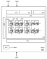
도 22의 (A)는 촬상 장치의 구성예를 도시한 블록도이고, 도 22의 (B)는 화소의 구성예를 도시한 회로도이다.
도 23의 (A) 및 도 23의 (B)는 전자 부품의 사시 모식도이다.
도 24의 (A) 내지 도 24의 (D)는 전자 기기의 구조예를 각각 도시한 도면이다.
도 25는 전자 부품의 회로부의 적층 구조예를 도시한 단면도이다.
도 26의 (A) 및 도 26의 (B)는 OS 트랜지스터의 구조예를 각각 도시한 단면도이다.1(A) and 1(B) are circuit diagrams showing a configuration example of a comparison circuit, and FIG. 1(C) is a diagram schematically showing drain current-gate voltage characteristics of a transistor.
2 is a circuit diagram showing a configuration example of a comparison circuit.
3(A) and 3(B) are circuit diagrams showing configuration examples of the comparison circuit.
4(A) to 4(C) are circuit diagrams each showing a configuration example of a comparison circuit.
5 is a circuit diagram showing a configuration example of a comparison circuit.
6 is a block diagram showing a structural example of a negative voltage supply device.
7 is a circuit diagram showing a configuration example of a charge pump circuit.
8(A) to 8(C) are circuit diagrams each showing a structural example of a charge pump circuit.
9(A) is a circuit diagram showing a configuration example of a negative voltage holding circuit, and FIG. 9(B) is a truth table of a driving circuit.
10 is a timing chart showing an operation example of a negative voltage supply device.
Fig. 11 is a block diagram showing a configuration example of a negative voltage supply device.
12 is a circuit diagram showing a structural example of a negative voltage holding circuit.
13(A) and 13(B) are circuit diagrams each showing a configuration example of a negative voltage holding circuit.
Fig. 14(A) is a block diagram showing a configuration example of a memory device, and Fig. 14(B) is a circuit diagram showing a configuration example of a memory cell.
15(A) to 15(F) are circuit diagrams each showing a configuration example of a memory cell.
Fig. 16(A) is a circuit diagram showing a configuration example of a memory cell, and Fig. 16(B) is a timing chart showing an operation example of the memory cell.
Fig. 17(A) is a circuit diagram showing a configuration example of a memory cell, and Fig. 17(B) is a timing chart showing an operation example of the memory cell.
Fig. 18 is a block diagram showing a structural example of a microcontroller unit.
Fig. 19 is a circuit diagram showing a structural example of a flip-flop.
Fig. 20 is a block diagram showing an example of the configuration of an FPGA.
FIG. 21(A) is a circuit diagram showing a configuration example of a routing switch, and FIG. 21(B) is a circuit diagram showing a configuration example of a configuration memory.
Fig. 22(A) is a block diagram showing a configuration example of an imaging device, and Fig. 22(B) is a circuit diagram showing a configuration example of pixels.
23(A) and 23(B) are perspective schematic views of electronic components.
24(A) to 24(D) are diagrams each showing a structural example of an electronic device.
25 is a cross-sectional view showing an example of a laminated structure of a circuit portion of an electronic component.
26(A) and 26(B) are cross-sectional views each showing a structural example of an OS transistor.
이하에서 본 발명의 실시형태에 대하여 설명한다. 또한, 본 발명의 일 형태는 이하의 설명에 한정되지 않는다. 본 발명의 취지 및 범위에서 벗어나지 않고 본 발명의 형태 및 자세한 사항을 다양하게 변경할 수 있다는 것은 통상의 기술자에 의하여 쉽게 이해될 것이다. 그러므로, 본 발명의 일 형태는 이하의 실시형태의 설명에 한정하여 해석되지 말아야 한다.EMBODIMENT OF THE INVENTION Embodiment of this invention is described below. In addition, one embodiment of the present invention is not limited to the following description. It will be readily understood by those skilled in the art that various changes can be made to the form and details of the present invention without departing from the spirit and scope of the present invention. Therefore, one aspect of the present invention should not be construed as limited to the description of the following embodiments.
아래에 기재된 임의의 실시형태는 적절히 조합될 수 있다. 하나의 실시형태에 몇 가지 구조예(제조 방법예 및 동작 방법예 등을 포함함)가 주어진 경우, 구조예 중 임의의 것을 서로 적절히 조합할 수 있거나, 또는 다른 실시형태에서 설명한 하나 이상의 구조예와 적절히 조합할 수 있다.Any of the embodiments described below may be appropriately combined. When several structural examples (including manufacturing method examples and operation method examples, etc.) are given in one embodiment, any of the structural examples can be appropriately combined with each other, or one or more structural examples described in other embodiments can be combined with each other. can be combined appropriately.
본 명세서 등에서, "제 1", "제 2", 및 "제 3" 등의 서수는 구성 요소들 사이의 혼동을 피하기 위하여 사용되고, 이 용어는 구성 요소를 수적으로 한정하거나 또는 순서를 한정하지 않는다.In this specification and the like, ordinal numbers such as "first", "second", and "third" are used to avoid confusion between components, and these terms do not limit the number of components or limit the order. .
도면에서, 동일한 구성 요소, 비슷한 기능을 갖는 구성 요소, 동일한 재료를 사용하여 형성되는 구성 요소, 및 동시에 형성되는 구성 요소 등은 동일한 부호로 나타내어지고, 그 설명은 반복되지 않는 경우가 있다.In the drawings, identical components, components having similar functions, components formed using the same materials, and components formed at the same time are denoted by the same reference numerals, and descriptions thereof are not repeated in some cases.
동일한 부호로 나타내어진 복수의 구성 요소를 서로 구별할 필요가 있을 때, 부호에 "_1", "_2", "[n]", 또는 "[m, n]" 등을 부기하는 경우가 있다.When it is necessary to distinguish a plurality of components indicated by the same code from each other, "_1", "_2", "[ n ]", or "[ m , n ]" may be added to the code.
본 명세서에서, 예를 들어, 전원 전압 VDD를 "전압 VDD" 또는 "VDD"라고 축약하는 경우가 있다. 다른 구성 요소(예를 들어, 신호, 전압, 회로, 소자, 전극, 및 배선)에 대해서도 마찬가지로 적용된다.In this specification, for example, the power supply voltage VDD may be abbreviated as “voltage VDD” or “VDD”. The same applies to other components (eg, signals, voltages, circuits, elements, electrodes, and wires).
도면에서, 크기, 층의 두께, 및 영역 등은 명료화를 위하여 과장되어 있는 경우가 있다. 그러므로, 크기, 층의 두께, 또는 영역은 도시된 스케일에 한정되지 않는다. 도면은 이상적인 예를 나타낸 모식도이고, 본 발명의 형태들은 도면에 나타낸 형상 또는 값에 한정되지 않는다. 예를 들어, 노이즈 또는 타이밍의 어긋남으로 인한 신호, 전압, 또는 전류의 편차가 포함될 수 있다.In the drawings, sizes, thicknesses of layers, areas, and the like are sometimes exaggerated for clarity. Therefore, the size, thickness of a layer, or area is not limited to the scale shown. The drawings are schematic diagrams showing ideal examples, and the forms of the present invention are not limited to the shapes or values shown in the drawings. For example, deviations in signals, voltages, or currents due to noise or misalignment of timing may be included.
본 명세서에서, "위에", "상방에", "아래에", 및 "하방에" 등의 배치를 설명하는 용어는 도면을 참조하여 구성 요소들 사이의 위치 관계를 설명하기 위하여 편의상 사용되는 경우가 있다. 또한, 구성 요소들 사이의 위치 관계는, 각 구성 요소를 설명하는 방향에 따라 적절히 변화된다. 따라서, 본 명세서에서 사용되는 용어에 대한 한정은 없고, 상황에 따라 적절히 설명할 수 있다.In this specification, terms describing arrangement such as "above", "above", "below", and "below" are used for convenience to describe the positional relationship between components with reference to the drawings. there is In addition, the positional relationship between components changes appropriately according to the direction in which each component is explained. Therefore, there is no limitation on terms used in this specification, and they can be appropriately described according to circumstances.
또한, 트랜지스터는 게이트, 소스, 및 드레인이라는 3개의 단자를 포함한다. 게이트는 트랜지스터의 도통 상태를 제어하는 제어 단자로서 기능한다. 트랜지스터의 형(type) 또는 단자에 공급되는 전위 레벨에 따라, 2개의 입출력 단자 중 한쪽이 소스로서 기능하고, 다른 쪽이 드레인으로서 기능한다. 그러므로, 본 명세서 등에서 "소스" 및 "드레인"이라는 용어를 서로 바꿀 수 있다. 본 명세서 등에서는, 게이트 이외의 2개의 단자를 제 1 단자 및 제 2 단자라고 하는 경우가 있다.Also, a transistor includes three terminals: a gate, a source, and a drain. The gate serves as a control terminal for controlling the conduction state of the transistor. Depending on the type of transistor or the potential level supplied to the terminal, one of the two input/output terminals functions as a source and the other functions as a drain. Therefore, the terms "source" and "drain" are interchangeable in this specification and the like. In this specification and the like, two terminals other than the gate are sometimes referred to as a first terminal and a second terminal.
회로 구성 또는 디바이스 구조 등에 따라, 노드를 단자, 배선, 전극, 도전층, 도전체, 또는 불순물 영역 등이라고 할 수 있다. 또한, 단자 또는 배선 등을 노드라고 할 수 있다.Depending on the circuit configuration or device structure, a node may be referred to as a terminal, wiring, electrode, conductive layer, conductor, impurity region, or the like. In addition, a terminal or wiring may be referred to as a node.
본 명세서 등에서, 경우 또는 상황에 따라 "막" 및 "층"이라는 용어를 서로 바꿀 수 있다. 예를 들어, "도전층"이라는 용어를 "도전막"이라는 용어로 바꿀 수 있는 경우가 있다. 예를 들어, "절연막"이라는 용어를 "절연층"이라는 용어로 바꿀 수 있는 경우가 있다.In this specification and the like, the terms "film" and "layer" may be interchanged depending on the case or circumstances. For example, there are cases where the term "conductive layer" can be replaced with the term "conductive film". For example, there are cases where the term "insulating film" can be replaced with the term "insulating layer".
본 명세서 등에서, 반도체 장치란 반도체 특성을 이용한 장치를 말하고, 반도체 소자(예를 들어, 트랜지스터 또는 다이오드)를 포함하는 회로 및 이 회로를 포함하는 장치 등을 의미한다. 반도체 장치는 반도체 특성을 이용함으로써 기능할 수 있는 어떤 장치도 의미한다. 예를 들어, 집적 회로, 및 집적 회로를 포함하는 칩은 반도체 장치의 예이다. 또한, 기억 장치, 표시 장치, 발광 장치, 조명 장치, 및 전자 기기 등은 이들 자체가 반도체 장치일 수 있거나, 또는 각각 반도체 장치를 포함할 수 있다.In this specification and the like, a semiconductor device refers to a device using semiconductor characteristics, and refers to a circuit including a semiconductor element (eg, a transistor or a diode) and a device including the circuit. A semiconductor device means any device that can function by utilizing semiconductor characteristics. For example, integrated circuits and chips including integrated circuits are examples of semiconductor devices. In addition, the memory device, the display device, the light emitting device, the lighting device, and the electronic device may themselves be semiconductor devices or each may include a semiconductor device.
(실시형태 1)(Embodiment 1)
본 실시형태에서는, 비교되는 음의 전압을 직접 입력할 수 있는 비교 회로, 및 이 비교 회로를 포함하는 반도체 장치에 대하여 설명한다.In this embodiment, a comparison circuit capable of directly inputting a negative voltage to be compared and a semiconductor device including the comparison circuit will be described.
≪비교 회로≫≪Comparator circuit≫
여기서는, 차동 증폭 회로를 사용하는 비교 회로의 구성예에 대하여 설명한다.Here, a configuration example of a comparison circuit using a differential amplifier circuit will be described.
도 1의 (A)는 비교 회로의 예를 도시한 것이다. 도 1의 (A)에 도시된 비교 회로(10)는 단자(INN), 단자(INP), 및 단자(OCM)를 포함한다. 단자(INN), 단자(INP), 및 단자(OCM)는 각각 반전 입력 단자, 비반전 입력 단자, 및 출력 단자이다.1(A) shows an example of a comparison circuit. The
비교 회로(10)에 전압 Vdda 및 전압 Vssa가 입력된다. 전압 Vdda는 고레벨 측 전원 전압이다. 전압 Vssa는 0V(접지 전압, GND) 등의 저레벨 측 전원 전압이다.Voltage Vdda and voltage Vssa are input to the
비교 회로(10)는 음의 참조 전압 Vnref와 음의 전압 Vnin을 비교하고, 비교 결과에 대응하는 전압 Vcmp를 단자(OCM)로부터 출력하는 기능을 갖는다. 음의 전압 Vnin은 단자(INP)에 입력된다. 음의 참조 전압 Vnref가 아니라, 양의 참조 전압 Vpref가 단자(INN)에 입력된다. 양의 참조 전압 Vpref는 양의 전압으로 변환된 음의 참조 전압 Vnref에 대응한다. 양의 참조 전압 Vpref의 값은 비교 회로(10)가 비교를 실행할 수 있도록 결정된다.The
도 1의 (B)는 비교 회로(10)의 회로 구성예를 도시한 것이다. 비교 회로(10)는 차동 회로로 구성되어 있고, 차동 쌍(14), 전류원(17), 및 부하 회로(18)를 포함한다.1(B) shows an example of the circuit configuration of the
차동 쌍(14)은 트랜지스터(MO11) 및 트랜지스터(MO12)를 포함한다. 트랜지스터(MO11) 및 트랜지스터(MO12)는 각각 백 게이트를 갖는 OS 트랜지스터이다. 트랜지스터(MO11)의 백 게이트는 단자(INP)에 전기적으로 접속되고, 전압 Vdda는 게이트에 입력된다. 트랜지스터(MO12)의 게이트는 단자(INN)에 전기적으로 접속되고, 전압 Vssa는 백 게이트에 입력된다.
여기서는, 트랜지스터(MO11)와 부하 회로(18) 사이의 접속 노드를 노드(X11)라고 하고, 트랜지스터(MO12)와 부하 회로(18) 사이의 접속 노드를 노드(X12)라고 하고, 트랜지스터(MO11)와 트랜지스터(MO12) 사이의 접속 노드를 노드(X13)라고 한다. 전류원(17)은 노드(X13)에 전류 Iss를 공급한다. 부하 회로(18)는 노드(X11) 및 노드(X12)에 각각 부하(Rd1) 및 부하(Rd2)를 준다.Here, the connection node between the transistor MO11 and the
또한, 도면에서는, 따로 명시되지 않는 한, 백 게이트를 갖는 n채널 트랜지스터는 OS 트랜지스터이고, p채널 트랜지스터 및 백 게이트를 갖지 않는 n채널 트랜지스터는 Si 트랜지스터이다.Also, in the figure, unless otherwise specified, an n-channel transistor with a back gate is an OS transistor, and a p-channel transistor and an n-channel transistor without a back gate are Si transistors.
노드(X12) 및 노드(X11)의 전압은 각각 트랜지스터(MO11)의 드레인 전류(Imo1)와 트랜지스터(MO12)의 드레인 전류(Imo2) 사이의 차이에 의하여 결정된다. 단자(OCM)가 노드(X12)에 전기적으로 접속되는 도 1의 (B)의 예에서는, Imo1>Imo2인 경우, 전압 Vcmp는 하이 레벨("H")이고, Imo1<Imo2인 경우, 전압 Vcmp는 로 레벨("L")이다.The voltages of the node X12 and the node X11 are determined by the difference between the drain current Imo1 of the transistor MO11 and the drain current Imo2 of the transistor MO12, respectively. In the example of FIG. 1(B) in which the terminal OCM is electrically connected to the node X12, when Imo1>Imo2, the voltage Vcmp is at a high level (“H”), and when Imo1<Imo2, the voltage Vcmp is the low level ("L").
(양의 참조 전압 Vpref의 설정예)(Example of setting positive reference voltage Vpref)
차동 쌍(14)을 흐르는 전류 Imo1과 전류 Imo2 사이의 차이를 단자(INP)와 단자(INN) 사이의 전압차로 환산할 수 있다. 따라서, 전압차에 따라 양의 참조 전압 Vpref를 설정할 수 있다. 구체적으로는, 단자(INP)의 전압, 트랜지스터(MO11)의 게이트 전압, 및 트랜지스터(MO12)의 백 게이트 전압이 각각 Vnref, Vdda, 및 Vssa인 경우, Imo1과 Imo2 사이의 차이가 0암페어일 때의, 단자(INP)와 단자(INN) 사이의 전압차를 추정한다. 추정된 전압차로부터 양의 참조 전압 Vpref의 값을 설정할 수 있다.The difference between the current Imo1 and the current Imo2 flowing through the
이러한 식으로 양의 참조 전압 Vpref를 설정함으로써, Vnin>Vnref인 경우, 단자(OCM)는 "H"의 전압 Vcmp를 출력하고, Vnin<Vnref인 경우, 단자(OCM)는 "L"의 전압 Vcmp를 출력한다.By setting the positive reference voltage Vpref in this way, when Vnin>Vnref, the terminal OCM outputs the voltage Vcmp of "H", and when Vnin<Vnref, the terminal OCM outputs the voltage Vcmp of "L". outputs
비교 회로(10)의 동작 원리에 대하여 도 1의 (C)를 참조하여 설명한다. 도 1의 (C)는 트랜지스터(MO11)의 드레인 전류-게이트 전압(Id-Vg) 특성을 모식적으로 나타낸 것이다. 곡선(9A)은 Vnin>Vnref일 때의 Id-Vg 곡선이다. 곡선(9B)은 Vnin<Vnref일 때의 Id-Vg 곡선이다.The operating principle of the
Vnin>Vnref인 경우, Imo1>Imo2이기 때문에, 전압 Vcmp는 "H"이다.When Vnin>Vnref, since Imo1>Imo2, the voltage Vcmp is "H".
백 게이트 전압의 저하는 트랜지스터(MO11)의 Vt를 양의 방향으로 시프트한다. 바꿔 말하면, 음의 전압 Vnin의 저하는 전류 Imo1을 저감시킨다. Vnin<Vnref인 경우, Imo1<Imo2이기 때문에, 전압 Vcmp는 "L"이다.A drop in the back gate voltage shifts the Vt of transistor MO11 in the positive direction. In other words, a decrease in the negative voltage Vnin reduces the current Imo1. When Vnin<Vnref, since Imo1<Imo2, the voltage Vcmp is "L".
다음에, 차동 쌍의 변형예에 대하여 설명한다. 도 1의 (A)의 예에서는, 차동 쌍(14)의 바이어스 전압으로서 전압 Vdda 및 전압 Vssa가 사용되지만, 바이어스 전압은 이들에 한정되지 않는다. 차동 쌍(14)의 바이어스 전압으로서 전압 Vdda 및 전압 Vssa를 사용함으로써, 비교 회로(10)에서 사용되는 전압의 종류를 저감할 수 있다.Next, a modified example of the differential pair will be described. In the example of FIG. 1(A), the voltage Vdda and the voltage Vssa are used as the bias voltages of the
또는, 트랜지스터(MO12)의 백 게이트를 단자(INP)에 전기적으로 접속하여도 좋고, 전압 Vssa 등의 바이어스 전압은 게이트에 입력된다.Alternatively, the back gate of the transistor MO12 may be electrically connected to the terminal INP, and a bias voltage such as voltage Vssa is input to the gate.
도 2에 도시된 비교 회로(11)는 차동 쌍(14) 대신에 차동 쌍(15)을 포함한다. 차동 쌍(15)은 트랜지스터(MO13) 및 트랜지스터(MO14)를 포함한다. 단자(INN)는 트랜지스터(MO13)의 게이트에 전기적으로 접속된다. 단자(INP)는 트랜지스터(MO14)의 게이트에 전기적으로 접속된다. 바이어스 전압(여기서는 Vdda)은 트랜지스터(MO13)의 백 게이트에 입력된다. 바이어스 전압(여기서는 Vssa)은 트랜지스터(MO14)의 백 게이트에 입력된다.The
트랜지스터(MO14)의 백 게이트를 단자(INP)에 전기적으로 접속하여도 좋고, 바이어스 전압(예를 들어, Vssa)은 게이트에 입력된다.The back gate of the transistor MO14 may be electrically connected to the terminal INP, and a bias voltage (eg, Vssa) is input to the gate.
비교 회로(10)는 복잡한 회로 구성 없이 비교되는 음의 전압을 직접 입력할 수 있다. 음의 참조 전압을 양의 참조 전압으로 변환함으로써, 비교되는 음의 전압(Vnin)을 제외한 0V 또는 양의 전압만이 비교 회로(10)에 입력되기 때문에, 비교 회로(10)의 동작이 안정된다. 이는 비교 회로(11)에 대해서도 마찬가지로 적용된다.The
<비교 회로(20) 내지 비교 회로(25)><
다음에, 비교 회로의 구체적인 회로 구성예에 대하여 설명한다.Next, a specific circuit configuration example of the comparison circuit will be described.
도 3의 (A)에 도시된 비교 회로(20)는 차동 입력 회로(30), 출력 회로(40), 및 단자(INN), 단자(INP), 및 단자(OCM)를 포함한다.The
차동 입력 회로(30)는 1단의 차동 증폭 회로이고, 차동 쌍(34) 및 트랜지스터(MN1), 트랜지스터(MP1), 및 트랜지스터(MP2)를 포함한다.The
차동 쌍(34)은 차동 쌍(14)과 동일한 회로 구성을 갖고 트랜지스터(MO1) 및 트랜지스터(MO2)를 포함한다. 트랜지스터(MO1)와 트랜지스터(MP1) 사이의 접속 노드를 노드(X1)라고 한다. 트랜지스터(MO2)와 트랜지스터(MP2) 사이의 접속 노드를 노드(X2)라고 한다.
단자(INP)는 트랜지스터(MO1)의 백 게이트에 전기적으로 접속된다. 단자(INN)는 트랜지스터(MO2)의 게이트에 전기적으로 접속된다. 전압 Vdda는 트랜지스터(MO1)의 게이트에 입력된다. 전압 Vssa는 트랜지스터(MO2)의 백 게이트에 입력된다.The terminal INP is electrically connected to the back gate of the transistor MO1. Terminal INN is electrically connected to the gate of transistor MO2. Voltage Vdda is input to the gate of transistor MO1. Voltage Vssa is input to the back gate of transistor MO2.
트랜지스터(MN1)는 전류원으로서 기능한다. 전압 Vb1은 트랜지스터(MN1)의 게이트에 입력된다. 전압 Vb1은 양의 전압이다.Transistor MN1 functions as a current source. Voltage Vb1 is input to the gate of transistor MN1. Voltage Vb1 is a positive voltage.
커런트 미러 회로는 트랜지스터(MP1) 및 트랜지스터(MP2)로 구성되어 있다. 커런트 미러 회로는 부하 회로로서 기능한다. 다이오드 접속된 트랜지스터(MP1) 및 트랜지스터(MP2)로 부하 회로를 구성하여도 좋다. 또는, 트랜지스터(MP1) 및 트랜지스터(MP2) 대신에 2개의 레지스터를 제공하여도 좋다.The current mirror circuit is composed of a transistor MP1 and a transistor MP2. The current mirror circuit functions as a load circuit. A load circuit may be constituted by diode-connected transistors MP1 and transistors MP2. Alternatively, two resistors may be provided in place of the transistors MP1 and MP2.
출력 회로(40)는 노드(X2)에 전기적으로 접속된다. 출력 회로(40)는 2단의 CMOS 인버터 회로로 구성되어 있다. CMOS 인버터 회로는 Si 트랜지스터로 구성되어 있다.
도 3의 (B)에 도시된 비교 회로(21)는 비교 회로(20)의 변형예이다. 출력 회로(41)는 1단의 CMOS 인버터 회로로 구성되어 있다. CMOS 인버터 회로의 입력 노드는 노드(X1)에 전기적으로 접속된다.The
도 4의 (A)에 도시된 비교 회로(22)는 비교 회로(20)의 변형예이다. 비교 회로(22)의 출력 회로(42)는 2단의 소스 폴로어 회로로 구성되어 있다. 도 4의 (B)에 도시된 비교 회로(23)는 비교 회로(22)의 변형예이다. 비교 회로(23)의 출력 회로(43)는 1단의 소스 폴로어 회로로 구성되어 있다. 소스 폴로어 회로의 입력 노드는 노드(X1)에 전기적으로 접속된다.The
도 4의 (C)에 도시된 비교 회로(24)는 비교 회로(21)의 변형예이고 차동 입력 회로(31)를 포함한다. 차동 입력 회로(31)는 차동 입력 회로(30)의 변형예이고, 트랜지스터(MN1) 대신에 트랜지스터(MO3)를 포함한다. 전압 Vb1은 트랜지스터(MO3)의 게이트에 입력되고, 백 게이트는 게이트에 전기적으로 접속된다. 또한, 트랜지스터(MO3)의 백 게이트에 바이어스 전압(예를 들어, 전압 Vssa)을 입력하여도 좋고, 백 게이트를 드레인에 전기적으로 접속하여도 좋다.The
비교 회로(20) 내지 비교 회로(24)는 Vnin>Vnref일 때 "H"의 전압 Vcmp를 출력하고, Vnin<Vnref일 때 "L"의 전압 Vcmp를 출력한다. 전압 Vcmp의 레벨과, Vnin과 Vnref 사이의 대소 관계 사이의 관계는 출력 회로의 회로 구성 등에 따라 적절히 변경된다.The
비교 회로(20)에서, 단자(INP)를 트랜지스터(MO1)의 게이트에 전기적으로 접속하여도 좋고, 트랜지스터(MO1)의 백 게이트에 바이어스 전압(예를 들어, Vdda)을 입력하여도 좋다. 단자(INN)를 트랜지스터(MO2)의 백 게이트에 전기적으로 접속하여도 좋고, 트랜지스터(MO2)의 게이트에 바이어스 전압(예를 들어, Vssa)을 입력하여도 좋다. 이는 비교 회로(21) 내지 비교 회로(24)에 대해서도 마찬가지로 적용할 수 있다.In the
≪다이내믹 비교 회로≫≪Dynamic Comparator Circuit≫
다이내믹 비교 회로의 구성예에 대하여 도 5를 참조하여 설명한다. 도 5에 도시된 비교 회로(25)는 차동 입력 회로(32), 출력 회로(45), 및 단자(INN), 단자(INP), 단자(OCM), 및 단자(OCMB)를 포함한다. 클록 신호(CLK)(이하, 신호(CLK)라고 함), 및 전압 Vdda 및 전압 Vssa는 비교 회로(25)에 입력된다.A configuration example of the dynamic comparison circuit will be described with reference to FIG. 5 . The
비교 회로(25)는 음의 참조 전압 Vnref와 음의 전압 Vnin을 비교하고, 비교 결과에 대응하는, 전압 Vcmp 및 전압 VcmpB를 단자(OCM) 및 단자(OCMB)로부터 출력한다. 음의 전압 Vnin 및 양의 참조 전압 Vpref는 각각 단자(INN) 및 단자(INP)에 입력된다. 양의 참조 전압 Vpref를 설정하는 방법은 비교 회로(10)와 비슷하다.The
도면에서의, 전류 Imo5 및 전류 Imo6은 각각 트랜지스터(MO5) 및 트랜지스터(MO6)의 드레인 전류를 의미한다.In the drawing, current Imo5 and current Imo6 mean drain currents of transistors MO5 and MO6, respectively.
비교 회로(25)에서는, 비교되는 음의 전압(Vnin)을 단자(INN)에 입력할 수 있고, 0V 이하의 전압을 사용할 수 있다.In the
차동 입력 회로(32)는 트랜지스터(MO5), 트랜지스터(MO6), 트랜지스터(MN5), 트랜지스터(MN6), 트랜지스터(MN7), 트랜지스터(MP5), 트랜지스터(MP6), 트랜지스터(MP7), 및 트랜지스터(MP8)를 포함한다.The
차동 입력 회로(32)의 차동 쌍은 차동 쌍(34)과 동일한 회로 구성을 갖고 트랜지스터(MO5) 및 트랜지스터(MO6)를 포함한다. 트랜지스터(MN7)는 전류원으로서 기능한다. 신호(CLK)는 트랜지스터(MN7)의 게이트에 입력된다.The differential pair of
여기서는, 트랜지스터(MN5)와 트랜지스터(MP5) 사이의 접속 노드를 노드(X5)라고 한다. 트랜지스터(MN6)와 트랜지스터(MP6) 사이의 접속 노드를 노드(X6)라고 한다. 래치 회로는 트랜지스터(MN5), 트랜지스터(MP5), 트랜지스터(MN6), 및 트랜지스터(MP6)로 구성되어 있다. 래치 회로는 전류 Imo5와 전류 Imo6 사이의 대소 관계에 기초하여 노드(X5) 및 노드(X6)의 전압 레벨을 결정한다.Here, the connection node between the transistor MN5 and the transistor MP5 is referred to as a node X5. A connection node between the transistor MN6 and the transistor MP6 is referred to as a node X6. The latch circuit is composed of a transistor MN5, a transistor MP5, a transistor MN6, and a transistor MP6. The latch circuit determines the voltage levels of node X5 and node X6 based on the magnitude relationship between current Imo5 and current Imo6.
트랜지스터(MP7) 및 트랜지스터(MP8)는 리셋 트랜지스터이다. 트랜지스터(MP7) 및 트랜지스터(MP8)의 온/오프는 신호(CLK)에 의하여 제어된다. 트랜지스터(MP7) 및 트랜지스터(MP8)가 온인 경우, 노드(X5) 및 노드(X6)의 전압은 Vdda("H")에 고정된다.Transistors MP7 and transistors MP8 are reset transistors. The on/off of the transistors MP7 and MP8 is controlled by the signal CLK. When transistors MP7 and MP8 are on, the voltages of nodes X5 and X6 are fixed at Vdda ("H").
출력 회로(45)는 인버터 회로(38) 및 인버터 회로(39)를 포함한다. 인버터 회로(38) 및 인버터 회로(39)의 입력 단자는 각각 노드(X5) 및 노드(X6)에 전기적으로 접속된다. 인버터 회로(38) 및 인버터 회로(39)의 출력 단자는 각각 단자(OCM) 및 단자(OCMB)에 전기적으로 접속된다.The
신호(CLK)가 "L"인 기간에, 비교 회로(25)는 프리차지를 수행한다. 트랜지스터(MP7) 및 트랜지스터(MP8)가 온이기 때문에, 노드(X5) 및 노드(X6)는 "H"에 고정되고, 단자(OCM) 및 단자(OCMB)는 "L"에 고정된다.During the period when the signal CLK is "L", the
신호(CLK)가 "H"인 기간에, 비교 회로(25)는 평가를 수행한다. 전류 Imo5와 전류 Imo6 사이에서 차이가 생길 때, 래치 회로에 포함되는 2개의 인버터 회로의 구동 능력 사이에서 차이가 생겨, 노드(X5)와 노드(X6) 사이에서 전압차가 생긴다.During the period when the signal CLK is "H", the
Vnin>Vnref인 경우, 전류 Imo5>전류 Imo6이다. 그러므로, 노드(X5)의 전압은 노드(X6)의 전압보다 낮고, 단자(OCM) 및 단자(OCMB)는 각각 "H" 및 "L"이다. 한편, Vnin<Vnref인 경우, 전류 Imo5<전류 Imo6이다. 그러므로, 노드(X5)의 전압은 노드(X6)의 전압보다 높고, 단자(OCM) 및 단자(OCMB)는 각각 "L" 및 "H"이다.When Vnin>Vnref, current Imo5>current Imo6. Therefore, the voltage of node X5 is lower than the voltage of node X6, and terminal OCM and terminal OCMB are "H" and "L", respectively. On the other hand, when Vnin<Vnref, current Imo5<current Imo6. Therefore, the voltage of node X5 is higher than that of node X6, and terminal OCM and terminal OCMB are "L" and "H", respectively.
도 3의 (A)에 도시된 비교 회로(20)의 차동 쌍은 백 게이트를 갖는 2개의 OS 트랜지스터로 형성되기 때문에, 전압 Vssa를 접지 전압으로 할 수 있다. 따라서, 음의 전압을 트랜지스터(MN1)의 소스에 입력할 필요는 없다.Since the differential pair of the
음의 전압이 n채널 Si 트랜지스터의 소스에 입력되면, p웰과 소스 영역 사이의 기생 다이오드(pn 접합 다이오드)에는 순방향 바이어스 전압이 인가된다. 이는 기판으로부터 소스 영역으로의 큰 전류의 역류를 일으킨다. 큰 전류의 역류를 방지하기 위하여, n채널 트랜지스터를 n웰로 둘러싼 트리플웰 구조(예를 들어, 특허문헌 3의 도 3의 (b) 및 도 6 참조)가 일반적으로 적용된다. 그러나, 트리플웰 n채널 트랜지스터로 인하여 회로 면적이 증가된다.When a negative voltage is input to the source of the n-channel Si transistor, a forward bias voltage is applied to a parasitic diode (pn junction diode) between the p-well and the source region. This causes a large current to flow back from the substrate to the source region. In order to prevent a large current from flowing backward, a triple well structure surrounding an n-channel transistor with n wells (eg, see FIG. 3(b) and FIG. 6 of Patent Document 3) is generally applied. However, the circuit area is increased due to the triple-well n-channel transistor.
트리플웰 n채널 Si 트랜지스터를 사용하지 않고 비교 회로(20)를 형성할 수 있기 때문에, 회로 면적을 축소할 수 있다. 이는 비교 회로(21) 내지 비교 회로(25)에 대해서도 마찬가지로 적용된다.Since the
상술한 바와 같이, 백 게이트를 갖는 2개의 n채널 트랜지스터로 형성되는 차동 쌍에 의하여, 본 실시형태에서의 비교 회로는 복잡한 회로 구성 없이, 비교되는 음의 전압이 공급될 수 있고, 음의 참조 전압을 양의 전압으로 변환함으로써 얻어지는 참조 전압을 사용할 수 있고, 그리고 저레벨 측 전원 전압을 0V(GND)로 할 수 있다. 따라서, 본 실시형태에서의 비교 회로는 음의 전압과 음의 참조 전압 사이에서 정확도가 높은 비교 및 안정된 동작을 수행할 수 있다.As described above, by the differential pair formed of two n-channel transistors with back gates, the comparison circuit in this embodiment can be supplied with a negative voltage to be compared without a complicated circuit configuration, and a negative reference voltage. A reference voltage obtained by converting to a positive voltage can be used, and the power supply voltage on the low level side can be set to 0V (GND). Therefore, the comparator circuit in this embodiment can perform highly accurate comparison and stable operation between the negative voltage and the negative reference voltage.
(실시형태 2)(Embodiment 2)
본 실시형태에서는, 실시형태 1에서 나타낸 비교 회로를 포함하는 반도체 장치에 대하여 설명한다. 일례로서 반도체 장치에 음의 전압을 공급하기 위한 장치에 대하여 설명한다.In this embodiment, a semiconductor device including the comparison circuit shown in
≪음의 전압 공급 장치(100)≫«Negative
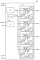
도 6은 음의 전압 공급 장치의 구조예를 도시한 블록도이다. 도 6에 도시된 음의 전압 공급 장치(100)는 내부에서 음의 전압을 생성하고, 생성된 음의 전압을 복수의 전원 단자에 출력한다. 음의 전압 공급 장치(100)는 제어 회로(111), 차지 펌프 회로(112), 바이어스 전압 생성 회로(114), 출력 전압 어저스터(120), 및 복수의 단자(OB)를 포함한다. 단자(OB)는 음의 전압용 출력 단자이다. 이 예에서 단자(OB)의 수는 4개이지만, 이에 한정되지 않는다.6 is a block diagram showing a structural example of a negative voltage supply device. The negative
4개의 단자(OB)를 구별하기 위하여, 부호[1] 내지 부호[4]를 사용한다. 복수의 단자(OB) 중 어느 하나를 지정할 필요가 있을 때, 예를 들어, 그 하나를 단자(OB[1])라고 한다. "단자(OB)"라는 용어는 임의의 단자(OB)를 말한다. 이는 다른 요소에 대해서도 마찬가지로 적용된다.In order to distinguish the four terminals (OB), codes [1] to codes [4] are used. When it is necessary to designate any one of a plurality of terminals OB, for example, that one is referred to as a terminal OB[1]. The term “terminal OB” refers to any terminal OB. This also applies to other elements.
양의 참조 전압 Vpref, 클록 신호(CK1), 신호(WAKE), 및 전압 Vdda, 전압 Vddd, 및 전압 GND는 음의 전압 공급 장치(100)에 입력된다. 또한, 전압 GND는 0V(접지 전압)이고, 음의 전압 공급 장치(100)의 저레벨 측 전원 전압으로서 사용된다. 전압 Vddd는 고레벨 측 전원 전압이고 전압 Vdda보다 낮다. 전압 Vddd는 제어 회로(111)에서 사용된다.The positive reference voltage Vpref, the clock signal CK1, the signal WAKE, and the voltage Vdda, the voltage Vddd, and the voltage GND are input to the negative
<제어 회로(111)><
신호(WAKE)는 음의 전압 공급 장치(100)의 이네이블 신호로서 기능한다. 제어 회로(111)는 신호(WAKE)에 따라 차지 펌프 회로(112) 및 출력 전압 어저스터(120)를 제어한다. 여기서, 제어 회로(111)는 게이티드 클록 버퍼로서 기능한다. 제어 회로(111)는 신호(WAKE)에 따라 클록 신호(CK1)로부터 게이티드 클록 신호(GCK1)(이하, 클록 신호(GCK1)라고 함)를 생성한다. 클록 신호(CK1)의 로 레벨 전압 및 하이 레벨 전압은 각각 GND 및 Vdda이다.The signal WAKE serves as an enable signal for the negative
클록 신호(GCK1)는 차지 펌프 회로(112) 및 출력 전압 어저스터(120) 각각에 입력된다.The clock signal GCK1 is input to each of the
<차지 펌프 회로(112)><
차지 펌프 회로(112)는 음의 전압 생성 회로로서 기능한다. 도 7은 차지 펌프 회로(112)의 회로 구성예를 도시한 것이고, 이 차지 펌프 회로는 4단 강압 차지 펌프 회로이다. 차지 펌프 회로(112)는 2개의 인버터 회로, 4개의 OS 트랜지스터, 4개의 용량 소자, 및 단자(IN_cp) 및 단자(OUT_cp)를 포함한다. 클록 신호(GCK1)가 액티브일 때, 차지 펌프 회로(112)는 단자(IN_cp)에 입력되는 전압 GND로부터 음의 전압 Vcp를 생성하고 단자(OUT_cp)로부터 음의 전압 Vcp를 출력한다.The
도 7의 예에서는, 4개의 트랜지스터가 단자(IN_cp)와 단자(OUT_cp) 사이의 전하 이동 경로에 제공되지만, 트랜지스터의 수는 이에 한정되지 않는다. 또한, 전하 이동 경로에 제공되는 트랜지스터는 OS 트랜지스터에 한정되지 않는다. 차지 펌프 회로(112)로서 사용할 수 있는 강압 차지 펌프 회로의 다른 예를 도 8의 (A) 내지 도 8의 (C)에 도시하였다.In the example of FIG. 7 , four transistors are provided in the charge transfer path between the terminal IN_cp and the terminal OUT_cp, but the number of transistors is not limited thereto. Also, the transistor provided for the charge transfer path is not limited to the OS transistor. Other examples of step-down charge pump circuits that can be used as the
도 8의 (A)의 차지 펌프 회로(113A)는 2개의 인버터 회로, 4개의 n채널 Si 트랜지스터, 및 4개의 용량 소자를 포함한다. 도 8의 (B)의 차지 펌프 회로(113B)는 3개의 n채널 Si 트랜지스터 및 하나의 OS 트랜지스터를 포함한다. 도 8의 (C)의 차지 펌프 회로(113C)는 2개의 인버터 회로, 4개의 p채널 Si 트랜지스터, 및 4개의 용량 소자를 포함한다.The
<바이어스 전압 생성 회로(114)><Bias
바이어스 전압 생성 회로(114)는 전압 Vb1을 생성한다. 전압 Vb1은 출력 전압 어저스터(120)에 입력된다. 바이어스 전압 생성 회로(114) 없이 외부로부터 전압 Vb1을 입력하여도 좋다.The bias
<출력 전압 어저스터(120)><
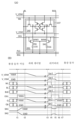
출력 전압 어저스터(120)는 각 단자(OB)로부터 음의 전압을 안정적으로 출력하기 위하여 제공된다. 출력 전압 어저스터(120)는 4개의 음의 전압 유지 회로(122)를 포함한다. 음의 전압 유지 회로(122)는 차지 펌프 회로(123), 구동 회로(127), 및 감시 회로(128)를 포함한다. 음의 전압 유지 회로(122[j])(j는 1 내지 4의 정수(整數)임)는 단자(OB[j])의 출력 전압을 제어한다. 도 9의 (A)는 음의 전압 유지 회로(122)의 회로 구성예를 도시한 것이다.The
<음의 전압 유지 회로(122)><Negative
차지 펌프 회로(123)는 트랜지스터(MO21) 및 트랜지스터(MO22), 및 용량 소자(C21) 및 용량 소자(C22)를 포함한다. 차지 펌프 회로(123)는 전압 Vcp를 저하시켜 전압 Vob를 생성한다. 전압 Vob는 용량 소자(C22)에 의하여 유지된다. 전압 Vob는 단자(OB)로부터 출력된다.The
용량 소자(C22)의 용량은 용량 소자(C21)의 용량보다 큰 것이 바람직하다. 예를 들어, 용량 소자(C22)의 용량은 용량 소자(C22)의 용량의 2배 내지 10배이다. 용량 소자(C21)에 요구되는 용량에 따라, 트랜지스터(MO21)의 기생 용량, 또는 트랜지스터(MO21)와 배선 사이의 기생 용량 등으로 용량 소자(C21)를 형성할 수 있다.The capacitance of the capacitance element C22 is preferably greater than the capacitance of the capacitance element C21. For example, the capacitance of the capacitance element C22 is 2 to 10 times the capacitance of the capacitance element C22. Depending on the capacitance required for the capacitance element C21, the capacitance element C21 can be formed with parasitic capacitance of the transistor MO21 or parasitic capacitance between the transistor MO21 and the wiring.
금속 산화물 반도체는 밴드 갭이 2.5eV 이상이기 때문에, OS 트랜지스터의 오프 상태 전류는 매우 작다. 예를 들어, 실온(25℃)에서, 그리고 3.5V의 소스-드레인 전압에서 채널 폭 1μm당 오프 상태 전류를 1×10-20A 미만, 1×10-22A 미만, 또는 1×10-24A 미만으로 할 수 있다. 즉, 드레인 전류의 온/오프비를 20자릿수 이상 150자릿수 이하로 할 수 있다.Since the metal oxide semiconductor has a band gap of 2.5 eV or more, the off-state current of the OS transistor is very small. For example, at room temperature (25° C.) and at a source-drain voltage of 3.5 V, the off-state current per μm channel width is less than 1×10 −20 A, less than 1×10 −22 A, or 1×10 −24 can be made less than A. That is, the on/off ratio of the drain current can be set to 20 digits or more and 150 digits or less.
금속 산화물 반도체는 에너지 갭이 크고 전자가 여기되기 어렵고 정공의 유효 질량이 큰 반도체이다. 따라서, OS 트랜지스터에서는 Si 트랜지스터보다 애벌란시 항복(avalanche breakdown) 등이 일어나기 어렵다. 애벌란시 항복으로 인한 핫 캐리어 열화 등이 억제되기 때문에, OS 트랜지스터는 소스와 드레인 사이에서 높은 내전압을 갖는다.A metal oxide semiconductor is a semiconductor with a large energy gap, difficult to excite electrons, and a large effective mass of holes. Therefore, avalanche breakdown or the like is less likely to occur in the OS transistor than in the Si transistor. Since hot carrier degradation and the like due to avalanche breakdown are suppressed, the OS transistor has a high withstand voltage between the source and drain.
채널 형성 영역에 사용할 수 있는 금속 산화물의 예에는 Zn 산화물, Zn-Sn 산화물, Ga-Sn 산화물, In-Ga 산화물, In-Zn 산화물, 및 In-M-Zn 산화물(M은 Ti, Ga, Y, Zr, La, Ce, Nd, Sn, 또는 Hf)이 포함된다. 또한, 인듐 및 아연을 함유하는 산화물은 알루미늄, 갈륨, 이트륨, 구리, 바나듐, 베릴륨, 붕소, 실리콘, 타이타늄, 철, 니켈, 저마늄, 지르코늄, 몰리브데넘, 란타넘, 세륨, 네오디뮴, 하프늄, 탄탈럼, 텅스텐, 및 마그네슘 등 중에서 선택되는 하나 이상의 종류의 원소를 함유하여도 좋다.Examples of metal oxides usable for the channel formation region include Zn oxide, Zn-Sn oxide, Ga-Sn oxide, In-Ga oxide, In-Zn oxide, and In-M-Zn oxide (M is Ti, Ga, Y , Zr, La, Ce, Nd, Sn, or Hf). In addition, oxides containing indium and zinc include aluminum, gallium, yttrium, copper, vanadium, beryllium, boron, silicon, titanium, iron, nickel, germanium, zirconium, molybdenum, lanthanum, cerium, neodymium, hafnium, It may contain one or more kinds of elements selected from tantalum, tungsten, magnesium, and the like.
음의 전압은 트랜지스터(MO22)의 게이트에 인가되기 때문에, 트랜지스터(MO22)의 백 게이트와 게이트의 전기적인 접속은 트랜지스터(MO22)의 컷오프 전류의 저감에 효과적이다. 이는 트랜지스터(MO22)의 백 게이트를 게이트에 전기적으로 접속함으로써, 트랜지스터(MO22)의 문턱 전압이 양의 방향으로 시프트되기 때문이다. 또한, 컷오프 전류는 트랜지스터의 게이트-소스 전압이 0V일 때의 드레인 전류를 말한다.Since a negative voltage is applied to the gate of the transistor MO22, electrical connection of the back gate and gate of the transistor MO22 is effective in reducing the cutoff current of the transistor MO22. This is because the threshold voltage of the transistor MO22 is shifted in the positive direction by electrically connecting the back gate of the transistor MO22 to the gate. Also, the cutoff current refers to the drain current when the gate-source voltage of the transistor is 0V.
그러므로, 트랜지스터(MO21) 및 트랜지스터(MO22)가 백 게이트를 갖는 OS 트랜지스터인 것은 장기간 음의 전압을 안정적으로 공급하는 데 효과적이다.Therefore, it is effective to stably supply a negative voltage for a long period of time when the transistors MO21 and MO22 are OS transistors having back gates.
OS 트랜지스터를 Si 트랜지스터 위에 적층할 수 있기 때문에, OS 트랜지스터인 트랜지스터(MO21) 및 트랜지스터(MO22)는 음의 전압 공급 장치(100)의 크기를 축소하는 데 효과적이다.Since the OS transistors can be stacked on top of the Si transistors, transistors MO21 and MO22, which are OS transistors, are effective in reducing the size of the negative
감시 회로(128)는 단자(OB)의 전압 Vob를 모니터한다. 감시 회로(128)는 차동 증폭 회로를 사용하는 비교 회로로 구성되어 있다. 도 9의 (A)에 도시된 비교 회로는 비교 회로(20)(도 3의 (A) 참조)의 변형예이다. 여기서, 출력 회로는 하나의 CMOS 인버터 회로를 포함한다.A
단자(INP)는 단자(OB)에 전기적으로 접속된다. 양의 참조 전압 Vpref는 단자(INN)에 입력된다. 단자(OCM)는 구동 회로(127)의 입력 단자에 전기적으로 접속된다. 신호(MON)는 단자(OCM)의 출력이다.Terminal INP is electrically connected to terminal OB. A positive reference voltage Vpref is input to the terminal INN. The terminal OCM is electrically connected to the input terminal of the driving
음의 전압 공급 장치(100)의 출력 전압을 음의 전압 VBG로 설정한다. 감시 회로(128)는 기준으로서 사용되는 음의 전압 VBG와, 전압 Vob를 비교한다. 감시 회로(128)가 이 비교를 수행할 수 있도록 양의 참조 전압 Vpref의 값을 설정한다.The output voltage of the negative
여기서, 감시 회로(128)는 전압 Vob의 저하를 모니터한다. 전압 Vob가 음의 전압 VBG보다 높은 경우, 감시 회로(128)는 "L"의 신호(MON)를 출력한다. 전압 Vob가 음의 전압 VBG 미만인 경우, 감시 회로(128)는 "H"의 신호(MON)를 출력한다.Here, the
복수의 감시 회로(128)들 사이의 특성(예를 들어, 오프셋 전압)의 편차에 따라, 복수의 양의 참조 전압을 사용하여도 좋다. 예를 들어, 서로 상이한 값을 갖는 2개의 양의 참조 전압(Vpref1 및 Vpref2)은 음의 전압 공급 장치(100)에 입력된다. 양의 참조 전압 Vpref1은 감시 회로(128[1]) 및 감시 회로(128[2])에 입력된다. 양의 참조 전압 Vpref2는 감시 회로(128[3]) 및 감시 회로(128[4])에 입력된다.Depending on variations in characteristics (eg, offset voltages) between the plurality of
구동 회로(127)는 신호(MON)와 클록 신호(GCK1) 사이에서 논리 연산을 수행하고 차지 펌프 회로(123)를 구동하기 위한 클록 신호(GCK2)를 생성한다. 구동 회로(127)는 신호(MON)가 "L"인 경우에 클록 신호(GCK2)가 액티브이고 다른 기간에서는 클록 신호(GCK2)가 비액티브인 회로 구성을 갖는다. 도 9의 (B)는 구동 회로(127)의 진리표의 예를 나타낸 것이다.The driving
≪동작예≫≪Example of operation≫
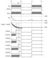
음의 전압 공급 장치(100)의 동작예에 대하여 도 10을 참조하여 설명한다. 도 10은 음의 전압 공급 장치(100)의 동작예를 나타낸 타이밍 차트이다. 시각을 t0 등으로 나타내었다. 여기서는, 시각(t0)에서, 차지 펌프 회로(112)의 출력 전압 Vcp 및 단자(OB[1]) 내지 단자(OB[4])의 전압 Vob[1] 내지 전압 Vob[4]는 0V(GND)이다.An operation example of the negative
도 10의 기간(Tc1)은 음의 전압 공급 장치(100)의 동작의 1주기이다. 신호(WAKE)는 음의 전압 공급 장치(100)의 칩 이네이블 신호로서 기능한다. 신호(WAKE)가 "H"인 기간에서는, 음의 전압 공급 장치(100)가 액티브이다.The period Tc1 of FIG. 10 is one cycle of the operation of the negative
신호(WAKE)가 "H"인 기간에서, 제어 회로(111)로부터 출력되는 클록 신호(GCK1)는 액티브이기 때문에, 차지 펌프 회로(112)는 강압 동작을 수행한다. 여기서는, 시각(t0)부터 시각(t1)까지 차지 펌프 회로(112)의 출력 전압 Vcp가 음의 전압 VBG에서 포화된다.During the period when the signal WAKE is "H", since the clock signal GCK1 output from the
시각(t0)에서 전압 Vob[1]는 GND이기 때문에, 감시 회로(128[1])로부터 "L"의 신호(MON[1])가 출력된다. 신호(MON[2]) 내지 신호(MON[4])도 "L"이다. 따라서, 구동 회로(127[1]) 내지 구동 회로(127[4])는 각각 액티브인 클록 신호(GCK2[1]) 내지 클록 신호(GCK2[4])를 출력한다.At time t0, since the voltage Vob[1] is GND, the "L" signal MON[1] is output from the monitoring circuit 128[1]. Signal MON[2] to signal MON[4] are also "L". Accordingly, the driving circuit 127[1] to the driving circuit 127[4] respectively output active clock signals GCK2[1] to clock signals GCK2[4].
차지 펌프 회로(123[1])는 강압 동작을 수행하기 때문에, 전압 Vob[1]는 저하된다. 차지 펌프 회로(123[2]) 내지 차지 펌프 회로(123[4])도 강압 동작을 수행한다.Since the charge pump circuit 123[1] performs a step-down operation, the voltage Vob[1] drops. The charge pump circuit 123 [2] to the charge pump circuit 123 [4] also perform a step-down operation.
차지 펌프 회로(123[1]) 내지 차지 펌프 회로(123[4]) 사이의 트랜지스터(MO21) 및 트랜지스터(MO22)의 전기 특성(예를 들어, 문턱 전압)의 편차는 차지 펌프 회로(123[1]) 내지 차지 펌프 회로(123[4]) 사이에서의 전류 구동 능력에 차이를 생기게 한다. 따라서, 단자(OB[1]) 내지 단자(OB[4])는 상이한 타이밍에서 음의 전압 VBG에 도달한다. 본 실시형태에서, 감시 회로(128[1]) 내지 감시 회로(128[4])는 독립적으로 단자(OB[1]) 내지 단자(OB[4])의 전압을 모니터하기 때문에, 단자(OB[1]) 내지 단자(OB[4]) 사이의 전압의 편차를 저감하여, 이들 전압을 음의 전압 VBG와 거의 동일하게 할 수 있다.Deviations in the electrical characteristics (eg, threshold voltage) of the transistors MO21 and MO22 between the charge pump circuit 123[1] and the charge pump circuit 123[4] are caused by the charge pump circuit 123[ 1]) to the charge pump circuit 123 [4]. Therefore, terminal OB[1] to terminal OB[4] reach negative voltage VBG at different timings. In this embodiment, since the monitoring circuit 128[1] to monitoring circuit 128[4] independently monitor the voltages of the terminals OB[1] to OB[4], the terminals OB [1]) to the terminal OB[4], it is possible to reduce the voltage variation, making these voltages substantially equal to the negative voltage VBG.
예를 들어, 음의 전압 유지 회로(122[1])에 대하여 설명한다. 감시 회로(128[1])는 전압 Vob[1]가 음의 전압 VBG에 도달한 것을 검출하면, "H"의 신호(MON[1])를 구동 회로(127[1])에 출력한다. "H"의 신호(MON[1])의 입력에 응하여, 구동 회로(127[1])는 클록 신호(GCK2)를 "H"에 고정한다. 그 결과, 차지 펌프 회로(123[1])는 강압 동작을 정지하고, 전압 Vob[1]는 거의 음의 전압 VBG로 설정된다.For example, the negative voltage holding circuit 122[1] will be described. When the monitoring circuit 128[1] detects that the voltage Vob[1] has reached the negative voltage VBG, it outputs a signal MON[1] of "H" to the driving circuit 127[1]. In response to the input of the "H" signal MON[1], the drive circuit 127[1] fixes the clock signal GCK2 to "H". As a result, the charge pump circuit 123[1] stops the step-down operation, and the voltage Vob[1] is set to a substantially negative voltage VBG.
트랜지스터(MO22[1])는 매우 작은 오프 상태 전류를 갖는 OS 트랜지스터이기 때문에, 클록 신호(GCK2)가 비액티브이어도 용량 소자(C22[1])는 장기간 음의 전압 VBG를 유지할 수 있다.Since the transistor MO22[1] is an OS transistor having a very small off-state current, the capacitor element C22[1] can maintain the negative voltage VBG for a long period of time even when the clock signal GCK2 is inactive.
음의 전압 유지 회로(122[2]) 내지 음의 전압 유지 회로(122[4])는 상술한 식으로 동작하고, 전압 Vob[2] 내지 전압 Vob[4]는 거의 음의 전압 VBG로 설정된다.Negative voltage holding circuit 122[2] to negative voltage holding circuit 122[4] operate in the above-described manner, and voltage Vob[2] to voltage Vob[4] are set to almost negative voltage VBG. do.
시각(t1)부터 시각(t2)까지 신호(WAKE)는 "L"이기 때문에, 음의 전압 공급 장치(100)는 비액티브이다. 여기서, 클록 게이팅을 수행하여 클록 신호(CK1)를 "L"에 고정함으로써, 음의 전압 공급 장치(100)의 대기 전력을 저감한다.Since the signal WAKE is "L" from time t1 to time t2,
음의 전압 유지 회로(122)의 우수한 유지 특성에 의하여 신호(WAKE)가 "L"인 기간을 길게 할 수 있다. 따라서, 이 기간에 음의 전압 공급 장치(100)로의 전원 전압(Vddd, Vdda)의 공급을 정지하기 위한 파워 게이팅을 수행할 수 있다. 파워 게이팅은 음의 전압 공급 장치(100)의 소비전력을 더 저감할 수 있다.Due to the excellent holding characteristics of the negative
도 10은 신호(WAKE)가 "L"인 기간에 파워 게이팅을 수행하는 예를 나타낸 것이다. 시각(t2)에서, 전압 Vddd 및 전압 Vdda의 공급이 개시되고, 신호(WAKE)가 "H"가 되고, 클록 신호(CK1)가 액티브가 된다. 시각(t2)부터 시각(t3)까지의 음의 전압 공급 장치(100)의 동작은 시각(t0)부터 시각(t1)까지의 동작과 비슷하다. 도 10에서, 시각(t1)부터 시각(t3)까지의 전압 Vob[1] 내지 전압 Vob[4]는 음의 전압 VBG를 넘지 않는다. 감시 회로(128[1]) 내지 감시 회로(128[4])가 액티브가 되면, "L"의 단자(OCM[1]) 내지 단자(OCM[4])는 "H"가 된다. 그러므로, 차지 펌프 회로(123[1]) 내지 차지 펌프 회로(123[4])는 대기 상태이다.10 illustrates an example of performing power gating during a period in which the signal WAKE is “L”. At time t2, supply of voltage Vddd and voltage Vdda starts, signal WAKE becomes "H", and clock signal CK1 becomes active. The operation of the negative
음의 전압 유지 회로(122)는 단자(OB)의 강압을 제어하는 기능 및 단자(OB)의 전압을 유지하는 기능을 갖기 때문에, 결정된 음의 전압을 장기간 안정적으로 단자(OB)로부터 출력할 수 있다.Since the negative
≪음의 전압 공급 장치(101)≫«Negative
음의 전압 공급 장치의 다른 구성예에 대하여, 도 11, 도 12, 및 도 13의 (A) 및 도 13의 (B)를 참조하여 설명한다. 이 구성예에서는, 음의 전압 감시 회로에 다이내믹 비교 회로를 사용한다.Another configuration example of the negative voltage supply device will be described with reference to FIGS. 11, 12, and 13(A) and 13(B). In this configuration example, a dynamic comparison circuit is used for the negative voltage monitoring circuit.
도 11에 도시된 음의 전압 공급 장치(101)는 제어 회로(141), 차지 펌프 회로(142), 분주 회로(143), 출력 전압 어저스터(150), 및 4개의 단자(OB)를 포함한다. 출력 전압 어저스터(150)는 4개의 음의 전압 유지 회로(152)를 포함한다.The negative
양의 참조 전압 Vpref, 클록 신호(CK1), 신호(WAKE), 및 전압 Vdda, 전압 Vddd, 및 전압 GND는 음의 전압 공급 장치(101)에 입력된다.The positive reference voltage Vpref, the clock signal CK1, the signal WAKE, and the voltage Vdda, the voltage Vddd, and the voltage GND are input to the negative
제어 회로(141)는 제어 회로(111)와 동일한 기능을 갖는다. 제어 회로(141)는 신호(WAKE)에 따라 클록 신호(GCK1)를 생성한다.The
차지 펌프 회로(142)는 차지 펌프 회로(112)와 동일한 회로 구성을 갖는다(도 7 참조). 차지 펌프 회로(142)는 클록 신호(GCK1)에 응하여 강압 동작을 수행하여 전압 Vcp를 출력한다.The
분주 회로(143)는 클록 신호(GCK1)의 분주를 수행하여 클록 신호(GCK3)를 생성한다. 클록 신호(GCK3)는 4개의 음의 전압 유지 회로(152) 각각에 입력된다.The
도 12는 음의 전압 유지 회로(152)의 회로 구성예를 도시한 것이다. 음의 전압 유지 회로(152)는 차지 펌프 회로(153), 구동 회로(154), 및 감시 회로(155)를 포함한다.12 shows an example of the circuit configuration of the negative
차지 펌프 회로(153)는 차지 펌프 회로(123)와 동일한 회로 구성을 갖고 트랜지스터(MO25) 및 트랜지스터(MO26), 및 용량 소자(C25) 및 용량 소자(C26)를 포함한다.The
구동 회로(154)는 구동 회로(127)와 비슷한 기능을 갖는다(도 9의 (B) 참조). 구동 회로(154)는 신호(MON)와 클록 신호(GCK3) 사이에서 논리 연산을 수행하고 차지 펌프 회로(153)를 구동하기 위한 클록 신호(GCK4)를 생성한다. 신호(MON)가 "L"인 경우, 클록 신호(GCK4)는 액티브이다. 신호(MON)가 "L"이 아닌 경우, 클록 신호(GCK4)는 비액티브이다.The driving
감시 회로(155)는 비교 회로(25)를 포함한다(도 5 참조). 클록 신호(GCK3)는 감시 회로(155)에 입력된다. 단자(INP)는 단자(OB)에 전기적으로 접속되고, 양의 참조 전압 Vpref는 단자(INN)에 입력된다. 단자(OCMB)는 구동 회로(154)의 입력 단자에 전기적으로 접속된다.The
여기서, 감시 회로(155)는 전압 Vob의 저하를 모니터한다. 전압 Vob가 음의 전압 VBG보다 높은 경우, 감시 회로(155)는 "L"의 신호(MON)를 출력한다. 전압 Vob가 음의 전압 VBG 미만인 경우, 감시 회로(155)는 "H"의 신호(MON)를 출력한다.Here, the
음의 전압 공급 장치(101)는 음의 전압 공급 장치(100)와 마찬가지로 동작을 수행한다(도 10 참조). 음의 전압 공급 장치(101)에서 신호(WAKE)가 "H"인 기간의 소비전력(즉, 동적 소비전력)은 음의 전압 공급 장치(100)보다 작다.The negative
신호(WAKE)가 "H"인 기간에서는, 클록 신호(GCK2)의 레벨에 상관없이 음의 전압 공급 장치(100)의 감시 회로(128)에는 전류가 항상 흐른다. 한편, 클록 신호(GCK3)가 "L"인 기간에서는, 감시 회로(155)의 출력(OCMB)이 "L"에 고정된다. 따라서, 감시 회로(155)의 소비 전류를 감시 회로(128)의 소비 전류보다 작게 할 수 있다.During the period when the signal WAKE is "H", current always flows in the
각 단자(OB)에 감시 회로(155)를 제공함으로써, 각 단자(OB)로부터 음의 전압을 안정적으로 출력할 수 있다. 그러나, 단자(OB)의 수가 증가될수록, 감시 회로(155)의 소비 전류의 영향이 커진다. 따라서, 감시 회로(155)의 소비 전류의 저감은 음의 전압 공급 장치(101) 전체의 동적 소비전력의 저감에 효과적이다.By providing the
동적 소비전력을 저감하기 위하여, 클록 신호를 저속으로 설정한다. 클록 신호(GCK1)를 저속으로 설정하면, 전압 Vcp가 음의 전압 VBG에 도달하는 데 시간이 걸린다. 바꿔 말하면, 신호(WAKE)가 "H"인 시간이 길어진다. 따라서, 클록 신호(GCK3)만을 저속으로 설정함으로써, 음의 전압 공급 장치(101)의 동적 소비전력을 효과적으로 저감할 수 있다.To reduce dynamic power consumption, the clock signal is set to a low speed. When the clock signal GCK1 is set to low speed, it takes time for the voltage Vcp to reach the negative voltage VBG. In other words, the time that the signal WAKE is "H" becomes longer. Accordingly, by setting only the clock signal GCK3 to a low speed, the dynamic power consumption of the negative
<감시 회로의 다른 구성예><Another configuration example of the monitoring circuit>
감시 회로(155)는 다이내믹 비교 회로로 구성되어 있기 때문에, 차동 쌍의 2개의 OS 트랜지스터를 동일한 양의 전류가 흐르면, 단자(OCM)의 신호(MON)는 불안정해질 수 있다. 다음에, 신호(MON)를 안정화시키는 방법에 대하여 도 13의 (A) 및 도 13의 (B)를 참조하여 설명한다.Since the
도 13의 (A)는 신호(MON)에 응하여 다이내믹 비교 회로의 양의 참조 전압을 전환하는 예를 도시한 것이다. 도 13의 (B)는 신호(MON)에 응하여 다이내믹 비교 회로의 차동 입력 회로의 전원 공급을 제어하는 예를 도시한 것이다.13(A) shows an example of switching the positive reference voltage of the dynamic comparison circuit in response to the signal MON. 13(B) shows an example of controlling the power supply of the differential input circuit of the dynamic comparison circuit in response to the signal MON.
(감시 회로(161))(supervisory circuit 161)
도 13의 (A)에 도시된 감시 회로(161)는 비교 회로(171), 래치 회로(173), 및 선택 회로(175)를 포함한다.The
비교 회로(171)는 비교 회로(25)로 구성되어 있다. 비교 회로(171)의 차동 쌍은 트랜지스터(MO7) 및 트랜지스터(MO8)로 구성되어 있다. 전류 Imo7 및 전류 Imo8은 각각 트랜지스터(MO7) 및 트랜지스터(MO8)의 드레인 전류이다.The
클록 신호(GCK3)의 상승과 동기하여 래치 회로(173)의 데이터는 비교 회로(171)의 출력에 의하여 갱신된다. 래치 회로(173)의 출력 신호는 신호(MON)이다. 예를 들어, 래치 회로(173)는 지연 플립플롭(DFF) 회로를 포함할 수 있다.Synchronized with the rise of the clock signal GCK3, the data of the
선택 회로(175)는 양의 참조 전압 Vpref 및 전압 GND 중에서 비교 회로(171)의 단자(INN)에 입력되는 전압을 선택한다. 신호(MON) 및 신호(WAKE)는 선택 회로(175)에 입력된다. 신호(WAKE)는 선택 회로(175)의 리셋 신호(RESET)로서 기능한다. 또한, 신호(WAKE) 이외의 신호를 리셋 신호로서 사용하여도 좋다.The
감시 회로(161)의 동작예에 대하여 설명한다. "L"의 신호(WAKE)가 "H"가 되면, 선택 회로(175)는 리셋되어 단자(INN)에 양의 참조 전압 Vpref를 공급한다. 클록 신호(GCK3)가 액티브일 때, 비교 회로(171)는 음의 전압 VBG와 단자(OB)의 전압 Vob를 비교한다. 전압 Vob가 음의 전압 VBG보다 높은 경우, 신호(MON)는 "L"이다. 신호(MON)가 "L"인 경우, 선택 회로(175)는 단자(INN)에 양의 참조 전압 Vpref를 입력한다.An operation example of the
전압 Vob가 음의 전압 VBG 미만이 되어 클록 신호(GCK3)가 "H"가 되면, "H"의 신호는 단자(OCMB)로부터 출력된다. 이때, 전류 Imo7이 전류 Imo8과 동등해짐으로써, 단자(OCMB)의 출력이 진동될 수 있다. 선택 회로(175)가 소정의 횟수(한 번 이상) 신호(MON)의 상승을 검출하면, 전압 GND는 단자(INN)에 공급된다. 그리고, 전류 Imo8이 저하되어 전류 Imo7과 전류 Imo8 사이에 차이가 생김으로써, 단자(OCMB)의 출력이 안정화된다. 클록 신호(GCK3)가 "H"일 때, 단자(OCMB)는 "H"의 신호를 안정적으로 출력할 수 있다.When the voltage Vob becomes less than the negative voltage VBG and the clock signal GCK3 becomes "H", a signal of "H" is outputted from the terminal OCMB. At this time, as the current Imo7 becomes equal to the current Imo8, the output of the terminal OCMB can be oscillated. When the
이 예에서, 전압 GND는 단자(INN)에 입력되지만, 신호(MON)가 "H"일 때에 전류 Imo7과 전류 Imo8 사이에 차이가 있기만 하면, 신호는 한정되지 않는다. 전압 Vpref보다 작은 양의 전압을 단자(INN)에 입력하여도 좋다. 전압 GND를 사용하면, 사용되는 전압의 종류가 증가되지 않는다.In this example, the voltage GND is input to the terminal INN, but the signal is not limited as long as there is a difference between the current Imo7 and the current Imo8 when the signal MON is "H". A positive voltage smaller than the voltage Vpref may be input to the terminal INN. Using the voltage GND does not increase the type of voltage used.
(감시 회로(162))(supervisory circuit 162)
도 13의 (B)에 도시된 감시 회로(162)는 비교 회로(172) 및 선택 회로(177)를 포함한다. 비교 회로(172)는 비교 회로(25)로 구성되어 있다. 감시 회로(161)와 같이, 감시 회로(162)에 래치 회로(173)를 제공하여도 좋다.The
선택 회로(177)는 비교 회로(172)의 차동 입력 회로(172A)로의 고레벨 측 전원 전압의 공급을 제어한다. 신호(MON) 및 신호(WAKE)는 선택 회로(177)에 입력된다. 신호(WAKE)는 선택 회로(177)의 리셋 신호로서 기능한다. 신호(WAKE) 이외의 신호를 리셋 신호로서 사용하여도 좋다.The
"L"의 신호(WAKE)가 "H"가 되면, 선택 회로(177)는 리셋되어 차동 입력 회로(172A)에 전압 Vdda를 공급한다. 클록 신호(GCK3)가 액티브일 때, 비교 회로(172)는 음의 전압 VBG와 단자(OB)의 전압 Vob를 비교한다. 선택 회로(177)가 소정의 횟수(한 번 이상) 신호(MON)의 상승을 검출하면, 전압 GND는 차동 입력 회로(172A)에 공급된다. 그 결과, 차동 입력 회로(172A)에서의 2개의 인버터 회로는 비액티브이기 때문에, 비교 회로(172)의 출력이 진동되지 않는다.When the signal WAKE of "L" becomes "H", the
본 실시형태에서의 음의 전압 공급 장치는 다양한 반도체 장치에서의 음의 전압 전원 회로에 적합하다. 이 음의 전압 공급 장치가 전원 회로로서 사용되는 반도체 장치로서는, 예를 들어, 기판 바이어스 전압이 음의 전압인 다양한 반도체 장치(예를 들어, DRAM 및 이미지 센서), 음의 전압에 의하여 구동되는 반도체 장치(예를 들어, 플래시 메모리 등의 기억 장치), 및 백 게이트를 갖는 OS 트랜지스터를 포함하는 반도체 장치가 있다. 실시형태 3에서는, 음의 전압 공급 장치를 포함하는 반도체 장치의 구조예에 대하여 설명한다.The negative voltage supply device in this embodiment is suitable for negative voltage power supply circuits in various semiconductor devices. As a semiconductor device for which this negative voltage supply device is used as a power supply circuit, for example, various semiconductor devices in which the substrate bias voltage is a negative voltage (e.g., DRAM and image sensor), semiconductors driven by a negative voltage device (for example, a storage device such as a flash memory), and a semiconductor device including an OS transistor having a back gate.
(실시형태 3)(Embodiment 3)
≪기억 장치≫≪Memory Device≫
여기서는, OS 트랜지스터를 사용하는 반도체 장치로서, 데이터 유지부가 OS 트랜지스터를 포함하는 기억 장치에 대하여 설명한다.Here, as a semiconductor device using an OS transistor, a storage device in which a data holding unit includes an OS transistor will be described.
도 14의 (A)에 도시된 기억 장치(200)는 음의 전압 공급 장치(210), 제어 회로(215), 메모리 셀 어레이(220), 및 주변 회로(221)를 포함한다. 주변 회로(221)는 행 회로(223), 열 회로(224), 및 입출력 회로(225)를 포함한다.The
메모리 셀 어레이(220)는 메모리 셀(230), 판독 워드선(RWL), 기록 워드선(WWL), 판독 비트선(RBL), 기록 비트선(WBL), 소스선(SL), 및 배선(BGL)을 포함한다. 또한, 판독 워드선(RWL) 및 기록 워드선(WWL)을 각각 워드선(RWL) 및 워드선(WWL)이라고 하여도 좋다. 판독 비트선(RBL) 및 기록 비트선(WBL)을 비트선(RBL) 및 비트선(WBL)이라고 하여도 좋다.The
제어 회로(215)는 기억 장치(200)를 통괄적으로 제어하고 데이터(WDA)의 기록 및 데이터(RDA)의 판독을 수행한다. 컨트롤러 회로(215)는 외부로부터의 명령 신호(예를 들어, 칩 이네이블 신호 및 기록 이네이블 신호)를 처리하고 주변 회로(221)의 제어 신호를 생성한다.The
음의 전압 공급 장치(210)로서 실시형태 2에서 설명한 음의 전압 공급 장치가 사용된다. 음의 전압 공급 장치(210)는 N개의 단자(OB[1]) 내지 단자(OB[N])(N은 2 이상의 정수임)를 포함한다. 단자(OB[1]) 내지 단자(OB[N])는 각각 음의 전압 Vbg1을 출력한다. 메모리 셀 어레이(220)는 N개의 블록으로 분할된다. 각 블록의 배선(BGL)은 단자(OB)에 전기적으로 접속된다.As the negative
행 회로(223)는 액세스되는 행을 선택하는 기능을 갖는다. 예를 들어, 행 회로(223)는 행 디코더 및 워드선 드라이버를 포함한다. 열 회로(224)는 비트선(WBL) 및 비트선(RBL)을 프리차지하는 기능, 비트선(WBL)에 데이터를 기록하는 기능, 비트선(RBL)의 데이터를 증폭하는 기능, 및 비트선(RBL)으로부터 데이터를 판독하는 기능 등을 갖는다. 입출력 회로(225)는 기록 데이터를 유지하는 기능 및 판독 데이터를 유지하는 기능 등을 갖는다.The
주변 회로(221)의 구성은 메모리 셀 어레이(220)의 구성, 판독 방법, 및 기록 방법 등에 따라 적절히 변경된다.The configuration of the
<메모리 셀(230)><
도 14의 (B)는 메모리 셀(230)의 회로 구성예를 도시한 것이다. 이 예에서의 메모리 셀(230)은 2-트랜지스터(2T) 게인 셀이다. 메모리 셀(230)은 용량 소자(CS1), 및 트랜지스터(MW1) 및 트랜지스터(MR1)를 포함한다. 트랜지스터(MW1) 및 트랜지스터(MR1)는 각각 기록 트랜지스터 및 판독 트랜지스터이다. 트랜지스터(MW1) 및 트랜지스터(MR1)의 백 게이트는 배선(BGL)에 전기적으로 접속된다.14(B) shows an example of the circuit configuration of the
판독 트랜지스터는 OS 트랜지스터이기 때문에, 메모리 셀(230)은 데이터 유지를 위하여 전력을 소비하지 않는다. 따라서, 메모리 셀(230)은 장기간 데이터를 유지할 수 있는 저소비전력 메모리 셀이다. 기억 장치(200)를 비휘발성 기억 장치로서 사용할 수 있다. OS 트랜지스터 및 용량 소자를 Si 트랜지스터 위에 적층할 수 있다. 따라서, 메모리 셀 어레이(220)를 주변 회로(221) 위에 적층 할 수 있어, 메모리 셀 어레이(220)의 집적도를 높일 수 있다.Since the read transistor is an OS transistor, the
메모리 셀의 다른 구성예에 대하여 도 15의 (A) 내지 도 15의 (F)를 참조하여 설명한다.Other structural examples of memory cells will be described with reference to FIGS. 15(A) to 15(F).
<메모리 셀(231) 내지 메모리 셀(235)><
도 15의 (A)에 도시된 메모리 셀(231)은 용량 소자(CS2), 및 트랜지스터(MW2), 트랜지스터(MR2), 및 트랜지스터(MS2)를 포함하는 3T 게인 셀이다. 트랜지스터(MW2), 트랜지스터(MR2), 및 트랜지스터(MS2)는 각각 기록 트랜지스터, 판독 트랜지스터, 및 선택 트랜지스터이다. 트랜지스터(MW2), 트랜지스터(MR2), 및 트랜지스터(MS2)의 백 게이트는 배선(BGL)에 전기적으로 접속된다. 메모리 셀(231)은 워드선(RWL) 및 워드선(WWL), 비트선(RBL) 및 비트선(WBL), 용량선(CDL), 및 전원선(PL2)에 전기적으로 접속된다. 예를 들어, 전압 GND(저레벨 측 전원 전압)는 용량선(CDL) 및 전원선(PL2)에 입력된다.The
도 15의 (B) 및 도 15의 (C)는 2T 게인 셀의 다른 구성예를 도시한 것이다. 도 15의 (B)에 도시된 메모리 셀(232)에서, n채널 Si 트랜지스터는 판독 트랜지스터로서 사용된다. 도 15의 (C)에 도시된 메모리 셀(233)에서, p채널 Si 트랜지스터는 판독 트랜지스터로서 사용된다.15(B) and 15(C) show another configuration example of a 2T gain cell. In the
도 15의 (D) 및 도 15의 (E)는 3T 게인 셀의 다른 구성예를 도시한 것이다. 도 15의 (D)에 도시된 메모리 셀(234)에서, n채널 Si 트랜지스터는 판독 트랜지스터 및 선택 트랜지스터로서 사용된다. 도 15의 (E)에 도시된 메모리 셀(235)에서, p채널 Si 트랜지스터는 판독 트랜지스터 및 선택 트랜지스터로서 사용된다. 도 15의 (E)의 예에서, 전압 Vddd(고레벨 측 전원 전압)는 전원선(PL2)에 입력된다.15(D) and 15(E) show another configuration example of a 3T gain cell. In the
이들 게인 셀에서, 판독 비트선(RBL) 및 기록 비트선(WBL)의 양쪽으로서 기능하는 비트선을 제공하여도 좋다.In these gain cells, bit lines that function as both the read bit line (RBL) and the write bit line (WBL) may be provided.
<메모리 셀(236)><
도 15의 (F)는 1T1C(용량 소자) 메모리 셀의 예를 도시한 것이다. 도 15의 (F)에 도시된 메모리 셀(236)은 워드선(WL), 비트선(BL), 용량선(CDL), 및 배선(BGL)에 전기적으로 접속된다. 메모리 셀(236)은 트랜지스터(MW3) 및 용량 소자(CS3)를 포함한다. 트랜지스터(MW3)의 백 게이트는 배선(BGL)에 전기적으로 접속된다.15(F) shows an example of a 1T1C (capacitance element) memory cell. The
<메모리 셀(237)><
도 16의 (A)에 도시된 메모리 셀(237)은 메모리 셀(240) 및 백업 회로(241)를 포함한다. 메모리 셀(240)은 일반적인 6T SRAM 셀과 동일한 회로 구성을 갖는다.The
백업 회로(241)는 메모리 셀(240)에 포함되는 노드(Q) 및 노드(Qb)의 데이터를 백업하기 위한 회로이고 2개의 1T1C 셀로 구성되어 있다. 노드(SN1) 및 노드(SN2)는 유지 노드이다. 트랜지스터(MW5) 및 용량 소자(CS5)로 구성되어 있는 게인 셀은 노드(Q)의 데이터를 백업한다. 트랜지스터(MW6) 및 용량 소자(CS6)로 구성되어 있는 게인 셀은 노드(Qb)의 데이터를 백업한다.The backup circuit 241 is a circuit for backing up data of the node Q and node Qb included in the
트랜지스터(MW5) 및 트랜지스터(MW6)는 OS 트랜지스터이기 때문에, 백업 회로(241) 위에 메모리 셀(240)을 적층할 수 있다. 따라서, 백업 회로(241)의 추가로 인한 메모리 셀(237)의 면적 오버헤드를 저감할 수 있다. 면적 오버헤드를 제로로 할 수 있다.Since the transistors MW5 and MW6 are OS transistors, the
메모리 셀(240)은 워드선(WL), 비트선쌍(BL 및 BLB), 및 전원선(V_VDM) 및 전원선(V_VSM)에 전기적으로 접속된다. 전원선(V_VDM) 및 전원선(V_VSM)은 각각 Vddd용 전원선 및 GND용 전원선이다. 백업 회로(241)는 전원선(PL3), 및 배선(OGL) 및 배선(BGL)에 전기적으로 접속된다. 전압 GND는 전원선(PL3)에 입력된다.The
통상 상태의 메모리 셀(237)은 SRAM 셀로서 동작한다. 메모리 셀(237)의 동작예에 대하여 도 16의 (B)를 참조하여 설명한다. 메모리 셀(237)이 소정의 시간 이상 액세스되지 않으면, 전원선(V_VDM) 및 전원선(V_VSM)으로의 전압 Vddd 및 전압 GND의 공급이 정지된다. 전압 Vddd의 공급이 정지되기 전에, 백업 회로(241)에 노드(Q) 및 노드(Qb)의 데이터가 기록된다. 도 16의 (B)에서는 시각을 t1 및 t2 등으로 나타내었다.The
(통상 동작)(normal operation)
시각(t1) 전에, 메모리 셀(237)은 통상 동작 상태(기록 상태 또는 판독 상태)에 있다. 메모리 셀(237)은 싱글 포트 SRAM과 비슷한 방법으로 동작한다. 시각(t1)에서 노드(Q) 및 노드(Qb)는 각각 "H" 및 "L"이고, 노드(SN1) 및 노드(SN2)는 각각 "L" 및 "H"이다.Before time t1, the
(백업)(back up)
t1에서, 배선(OGL)이 "H"가 됨으로써, 백업 동작이 개시되고, 트랜지스터(MW5) 및 트랜지스터(MW6)는 온이 된다. 노드(SN1)의 전압은 GND로부터 Vddd로 상승된다. 노드(SN2)의 전압은 Vddd로부터 GND로 저하된다. t2에서 배선(OGL)이 "L"이 됨으로써, 백업 동작이 종료된다. t1에서의 노드(Q)의 데이터 및 노드(Qb)의 데이터는 각각 노드(SN1) 및 노드(SN2)에 기록된다.At t1, when the wiring OGL goes to "H", the backup operation starts, and the transistors MW5 and MW6 are turned on. The voltage at node SN1 rises from GND to Vddd. The voltage at node SN2 drops from Vddd to GND. At t2, when the wire OGL becomes "L", the backup operation ends. The data of the node Q and the data of the node Qb at t1 are written to the nodes SN1 and SN2, respectively.
(파워 게이팅)(power gating)
t2에서 파워 게이팅이 개시된다. 전원선(V_VDM)의 전압은 Vddd로부터 GND로 변화된다. 전원선(V_VDM)과 전원선(V_VSM) 사이의 전압차가 작아짐으로써, 메모리 셀(240)은 비액티브가 된다. 메모리 셀(240)의 데이터는 소실되지만, 백업 회로(241)는 데이터를 연속적으로 유지한다. 파워 게이팅 동안, 비트선쌍(BL 및 BLB)은 부유 상태에 있다.At t2, power gating is initiated. The voltage of the power supply line (V_VDM) is changed from Vddd to GND. As the voltage difference between the power line V_VDM and the power line V_VSM decreases, the
(리커버리)(recovery)
리커버리 동작이란 백업 회로(241)에 유지된 데이터를 사용하여 메모리 셀(240)의 데이터를 리커버리하는 동작을 말한다. 리커버리 동작에서, 메모리 셀(240)은 노드(Q) 및 노드(Qb)의 데이터를 검지하기 위한 센스 앰프로서 기능한다.The recovery operation refers to an operation of recovering data of the
우선, 노드(Q) 및 노드(Qb)의 리셋 동작을 수행한다. t3에서, 비트선쌍(BL 및 BLB)의 전압은 전압 Vpr2로 프리차지된다. 또한, 워드선(WL)이 선택된다. 따라서, 전원선(V_VDM) 및 전원선(V_VSM)은 전압 Vpr2로 프리차지되고, 노드(Q) 및 노드(Qb)의 전압은 Vpr2에 고정된다.First, a reset operation of the node Q and the node Qb is performed. At t3, the voltage of the bit line pair BL and BLB is precharged to the voltage Vpr2. Also, the word line WL is selected. Accordingly, the power supply line V_VDM and the power supply line V_VSM are precharged to the voltage Vpr2, and the voltages of the node Q and the node Qb are fixed to Vpr2.
t4에서 배선(OGL)이 "H"가 됨으로써, 트랜지스터(MW5) 및 트랜지스터(MW6)는 온이 된다. 용량 소자(CS5)의 전하는 노드(Q) 및 노드(SN1)에 분배된다. 용량 소자(CS6)의 전하는 노드(Qb) 및 노드(SN2)에 분배된다. 그 결과, 노드(Q)와 노드(Qb) 사이에서 전압차가 생긴다.At t4, when the wiring OGL becomes "H", the transistors MW5 and MW6 are turned on. The charge of the capacitive element CS5 is distributed to the node Q and the node SN1. The charge of the capacitive element CS6 is distributed to the node Qb and the node SN2. As a result, a voltage difference is generated between node Q and node Qb.
t5에서 전압 VDM 및 전압 GND의 공급을 재개한다. 메모리 셀(240)이 액티브가 되어 노드(Q)와 노드(Qb) 사이의 전압차가 증폭된다. 마지막으로, 노드(Q) 및 노드(SN1)의 전압은 Vddd가 되고, 노드(Qb) 및 노드(SN2)의 전압은 GND가 된다. 바꿔 말하면, 노드(Q) 및 노드(Qb)의 상태는 각각 t1의 상태, 즉 "H" 및 "L"로 복귀한다.At t5, supply of voltage VDM and voltage GND is resumed. As the
<메모리 셀(238)><
도 17의 (A)에 도시된 메모리 셀(238)은 메모리 셀(237)의 변형예이고 백업 회로(241) 대신에 백업 회로(242)를 포함한다. 백업 회로(242)는 하나의 1T1C 메모리 셀로 구성되어 있고 노드(SN3), 트랜지스터(MW7), 및 용량 소자(CS7)를 포함한다.The
도 17의 (B)는 메모리 셀(238)의 동작예를 나타낸 타이밍 차트이다. 메모리 셀(238)은 메모리 셀(237)과 비슷한 방법으로 동작한다. 도 17의 (B)의 설명에 대해서는 도 16의 (B)의 설명을 참조할 수 있다.17(B) is a timing chart showing an example of the operation of the
백업 회로(242)는 노드(Q)의 데이터만을 백업하지만, 노드(SN3)에 유지된 데이터로 노드(Q) 및 노드(Qb)의 데이터를 복원할 수 있다. 이는 노드(Q) 및 노드(Qb)가 미리 Vpr2로 프리차지되기 때문이고, 이로써 하나의 용량 소자(CS7)의 전하를 사용하여 노드(Q)와 노드(Qb) 사이에 전위차를 발생시킬 수 있다.The
본 명세서 등에서는, 메모리 셀 등의 데이터 유지부가 OS 트랜지스터를 포함하는 기억 장치를 OS 기억 장치라고 하는 경우가 있다. OS 기억 장치의 예에는 DOSRAM(등록 상표), NOSRAM(등록 상표), 및 OS-SRAM 등이 포함된다.In this specification and the like, a storage device in which a data holding unit such as a memory cell includes an OS transistor is sometimes referred to as an OS storage device. Examples of the OS storage device include DOSRAM (registered trademark), NOSRAM (registered trademark), OS-SRAM, and the like.
DOSRAM이란 Dynamic Oxide Semiconductor RAM의 약칭이고, 1T1C 메모리 셀(도 15의 (F) 참조)을 포함하는 RAM을 나타낸다. NOSRAM이란 Nonvolatile Oxide Semiconductor RAM의 약칭이고, 게인 셀(도 14의 (A) 및 도 15의 (A) 내지 도 15의 (D) 참조)을 포함하는 RAM을 나타낸다. OS-SRAM은 백업 회로를 포함하는 SRAM 셀(도 16의 (A) 및 도 17의 (A) 참조)을 포함하는 RAM을 나타낸다.DOSRAM is an abbreviation for Dynamic Oxide Semiconductor RAM, and represents RAM including 1T1C memory cells (see (F) in FIG. 15). NOSRAM is an abbreviation of Nonvolatile Oxide Semiconductor RAM, and represents RAM including gain cells (see FIGS. 14(A) and 15(A) to 15(D)). OS-SRAM refers to a RAM including SRAM cells (see Figs. 16(A) and 17(A)) including backup circuits.
다음에, 반도체 장치의 일례로서 처리 장치에 대하여 설명한다. 여기서는, 마이크로 컨트롤러 유닛(MCU) 및 FPGA를 예로서 나타낸다.Next, a processing device will be described as an example of a semiconductor device. Here, microcontroller units (MCUs) and FPGAs are shown as examples.
≪MCU≫«MCUs»
도 18의 MCU(250)는 클록 게이팅 및 파워 게이팅이 가능한 반도체 장치이다.The
전압 Vddd, 전압 Vdda, 및 전압 GND는 MCU(250)에 입력된다. MCU(250)는 PMU(power management unit)(260), 음의 전압 공급 장치(261), 버스(262), 파워 스위치(264) 및 파워 스위치(265), 레벨 시프터(LS) 및 버퍼 회로(267), 프로세서 코어(270)(이하, 코어(270)라고 함), 및 기억 장치(280)를 포함한다. PMU(260), 코어(270), 및 기억 장치(280)와의 데이터 등의 교환은 버스(262)를 통하여 수행된다.Voltage Vddd, voltage Vdda, and voltage GND are input to
반도체 장치의 소비전력을 저감하기 위하여, 동작시킬 필요가 없는 회로는 파워 게이팅 또는 클록 게이팅에 의하여 정지된다. 플립플롭은 반도체 장치에 포함되는 순서 회로(상태를 유지하는 저장 회로)의 일종인 경우가 많다. 따라서, 플립플롭의 소비전력 저감은 플립플롭을 포함하는 반도체 장치의 소비전력 저감에 효과적이다. 일반적으로, 전원이 정지되면, 플립플롭의 상태는 소거된다(거기에 유지된 데이터가 소실된다). 따라서, 반도체 장치를 파워 게이팅하기 위하여 플립플롭의 상태를 백업할 필요가 있다.In order to reduce the power consumption of the semiconductor device, circuits that do not need to be operated are stopped by power gating or clock gating. Flip-flops are often a type of sequential circuits (storage circuits that hold states) included in semiconductor devices. Therefore, reducing the power consumption of the flip-flop is effective in reducing the power consumption of the semiconductor device including the flip-flop. Generally, when the power is turned off, the flip-flop's state is cleared (the data held on it is lost). Therefore, it is necessary to back up the state of the flip-flop in order to power gate the semiconductor device.
코어(270)는 복수의 플립플롭(271)을 포함한다. 플립플롭(271)은 코어(270)의 다양한 레지스터에 제공된다. 플립플롭(271)은 백업 회로(272) 및 스캔 플립플롭(273)을 포함한다. 바꿔 말하면, 플립플롭(271)은 백업 회로를 포함하는 스캔 플립플롭이다.The
클록 게이팅 및 파워 게이팅 시에, 플립플롭(271)의 데이터를 저장하기 위하여, 플립플롭(271)에는 백업 회로(272)가 제공된다. 백업 회로(272)는 백 게이트를 갖는 복수의 OS 트랜지스터를 포함한다. 백업 회로(272)에는 Si 트랜지스터가 포함되지 않기 때문에, Si 트랜지스터로 구성되어 있는 논리 셀 위에 백업 회로(272)를 적층할 수 있다. 도 19는 플립플롭(271)의 회로 구성예를 도시한 것이다.In order to store data of the flip-
스캔 플립플롭(273)은 클록 버퍼 회로(273A), 및 노드(D1), 노드(Q1), 노드(SD), 노드(SE), 노드(RT), 및 노드(CK10)를 포함한다.The scan flip-
노드(D1)는 데이터 입력 노드이고, 노드(Q1)는 데이터 출력 노드이고, 그리고 노드(SD)는 스캔 테스트 데이터 입력 노드이다. 노드(SE)는 신호(SCE) 입력 노드이다. 노드(CK10)는 클록 신호(GCLK10) 입력 노드이다. 클록 신호(GCLK10)는 클록 버퍼 회로(272A)에 입력된다. 스캔 플립플롭(273)의 각 아날로그 스위치는 클록 버퍼 회로(273A)의 노드(CK11) 및 노드(CKB11)에 전기적으로 접속된다. 노드(RT)는 리셋 신호 입력 노드이다.Node D1 is a data input node, node Q1 is a data output node, and node SD is a scan test data input node. Node SE is a signal SCE input node. Node CK10 is a clock signal GCLK10 input node. The clock signal GCLK10 is input to the clock buffer circuit 272A. Each analog switch of the scan flip-
신호(SCE)가 "L"인 경우, 스캔 플립플롭(273)에는 노드(D1)의 데이터가 입력된다. 신호(SCE)가 "H"인 경우, 스캔 플립플롭(273)에는 노드(SD)의 데이터가 입력된다.When the signal SCE is “L”, the data of the node D1 is input to the scan flip-
스캔 플립플롭(273)의 회로 구성은 도 19의 회로 구성에 한정되지 않는다. 표준적인 회로 라이브러리에 준비된 어느 스캔 플립플롭이나 사용할 수 있다.The circuit configuration of the scan flip-
백업 회로(272)는 노드(SD_IN) 및 노드(SN11), 트랜지스터(MO11) 내지 트랜지스터(MO13), 용량 소자(C11), 및 노드(SN11)를 포함한다. 트랜지스터(MO11)의 온/오프 및 트랜지스터(MO13)의 온/오프는 신호(BKH)에 의하여 제어되고, 트랜지스터(MO12)의 온/오프는 신호(RCH)에 의하여 제어된다. 트랜지스터(MO11) 내지 트랜지스터(MO13)의 백 게이트는 CPU 코어(330)의 배선(BGL2)에 전기적으로 접속된다. 음의 전압 Vbg2는 배선(BGL1)에 입력된다.The
노드(SD_IN)는 스캔 테스트 데이터 입력 노드이고 다른 스캔 플립플롭(273)의 노드(Q1)에 전기적으로 접속된다. 노드(SN11)는 백업 회로(340)의 유지 노드이다.Node SD_IN is a scan test data input node and is electrically connected to node Q1 of another scan flip-
오프 상태 전류가 매우 낮다는 OS 트랜지스터의 특징 때문에, 노드(SN11)의 전압 저하를 방지할 수 있고 데이터를 유지하는 데 전력이 거의 소비되지 않으므로, 백업 회로(272)는 장기간의 데이터 유지가 가능하다, 즉, 비휘발성이다. 따라서, CPU 코어(330)가 파워 게이팅 상태에 있을 때, 백업 회로(340)에 데이터를 유지할 수 있다.Due to the feature of the OS transistor that the off-state current is very low, the voltage drop of the node SN11 can be prevented and little power is consumed to retain data, so the
기억 장치(280)는 제어 회로(281), 주변 회로(282), 및 메모리 셀 어레이(283)를 포함한다. 기억 장치(280)에는 OS 기억 장치를 적용할 수 있다.The
음의 전압 공급 장치(261)로서 실시형태 2에서의 음의 전압 공급 장치가 사용된다. 음의 전압 공급 장치(261)는 전압 GND로부터 음의 전압 Vbg1 및 음의 전압 Vbg2를 생성한다. 음의 전압 공급 장치(261)는 Vbg1 출력용의 복수의 단자(OB1), 및 Vbg2 출력용의 복수의 단자(OB2)를 포함한다. 음의 전압 Vbg1 및 음의 전압 Vbg2는 각각 기억 장치(280) 및 코어(270)에 입력된다.As the negative
클록 신호 및 인터럽트 요구 신호 등이 외부로부터 MCU(250)에 입력된다. 외부 클록 신호는 PMU(260)에 입력된다. 인터럽트 요구 신호는 PMU(260) 및 코어(270)에 입력된다.A clock signal and an interrupt request signal are input to the
PMU(260)는 클록 게이팅 및 파워 게이팅을 제어하는 기능을 갖는다. PMU(260)는 외부 클록 신호로부터 게이티드 클록 신호(GCK10)(이하, GCLK10이라고 함)를 생성한다. 클록 신호(GCLK10)는 코어(270) 및 기억 장치(280)에 입력된다. PMU(260)는 다양한 제어 신호를 생성한다. 제어 신호는 파워 스위치(264) 및 파워 스위치(265)의 제어 신호, 백업 회로(272)의 제어 신호, 및 스캔 플립플롭(273)의 제어 신호(예를 들어, 리셋 신호)를 포함한다.The
백업 회로(272)의 제어 신호는 LS 및 버퍼 회로(267)에 입력된다. LS 및 버퍼 회로(267)는 제어 신호를 레벨 시프트하는 기능 및 레벨 시프트된 제어 신호를 유지하는 기능을 갖는다. LS 및 버퍼 회로(267)에 의하여 유지되는 제어 신호는 백업 회로(272)에 입력된다.A control signal of the
파워 스위치(264)는 코어(270)로의 전압 Vddd의 공급을 제어한다. 파워 스위치(265)는 기억 장치(280)로의 전압 Vddd 및 전압 Vdda의 공급을 제어한다. 코어(270)가 복수의 전원 도메인을 포함하는 경우, 전원 도메인에 대응하는 파워 스위치를 파워 스위치(264)로서 제공한다. 파워 스위치(265)에 대해서도 마찬가지로 적용된다. 전압 Vddd 및 전압 Vdda 이외에, 회로 구성에 따른 복수의 양의 전압이 기억 장치(280)에 입력된다. 기억 장치(280)에 입력되는 양의 전압은 비트선의 프리차지용 전압, 및 데이터 판독용의 참조 전압 등이다.
신호(SLEEP)는 코어(270)로부터 PMU(260)에 출력된다. 신호(SLEEP)는 코어(270)를 슬리프 모드(대기 모드)로 하기 위한 트리거 신호이다. PMU(260)에 신호(SLEEP)가 입력되면, PMU(260)는 액티브 모드에서 슬리프 모드로의 이행을 위한 제어 신호를, 제어되는 기능 회로에 출력한다. 인터럽트 요구 신호의 입력에 의해서도 액티브 모드에서 슬리프 모드로의 이행을 수행할 수 있다.Signal SLEEP is output from
액티브 모드에서 슬리프 모드로 이행하기 위하여, 우선, PMU(260)는 코어(270)로의 클록 신호의 공급을 정지한다. 그리고, 스캔 플립플롭(273)의 데이터를 백업 회로(272)에 기록한다. 구체적으로는, "H"의 신호(BKH)를 백업 회로(272)에 소정의 클록 사이클 동안 입력한다.To transition from the active mode to the sleep mode, first, the
코어(270)를 슬리프 모드에서 액티브 모드로 복귀하기 위한 처리는, 예를 들어, 인터럽트 요구 신호의 입력에 의하여 실행된다. 인터럽트 요구 신호에 응하여, PMU(260)는 슬리프 모드에서 액티브 모드로의 이행을 위한 제어 신호를, 제어되는 기능 회로에 출력한다. PMU(260)는 파워 스위치(264) 및 파워 스위치(265)를 제어하여, 코어(270) 및 기억 장치(280)로의 전위의 공급을 재개한다. 그리고, 백업 회로(272)에 유지된 데이터를 스캔 플립플롭(273)에 리커버리한다. 구체적으로는, 백업 회로(272)에 소정의 클록 사이클 동안 "H"의 신호(BCH)를 입력하고, 스캔 플립플롭(273)에 "H"의 신호(SCE)를 입력한다. 마지막으로, 코어(270) 및 기억 장치(280)로의 클록 신호(GCLK10)의 공급을 재개한다.Processing for returning the core 270 from the sleep mode to the active mode is executed by input of an interrupt request signal, for example. In response to the interrupt request signal, the
PMU(260)는 코어(270)와 같이, 기억 장치(280)의 클록 게이팅 및 파워 게이팅을 수행한다.Like the
시간을 계측하기 위한 타이머 회로는, 계측되는 시간에 기초하여 코어(270) 및 기억 장치(280)를 파워 게이팅하기 위하여 PMU(260)에 제공되어도 좋다.A timer circuit for counting the time may be provided in the
≪FPGA≫≪FPGA≫
도 20은 FPGA의 예를 도시한 것이다. 도 20에 도시된 FPGA(400)는 음의 전압 공급 장치(405), 로직 어레이(410), 입축력 유닛(I/O)(411), 및 주변 회로를 포함한다. FPGA(400)에 하나 이상의 OS 기억 장치를 제공하여도 좋다.20 shows an example of an FPGA. The
I/O(411)는 로직 어레이(410)의 입출력 인터페이스이다. 주변 회로는 로직 어레이(410) 및 I/O(411)를 구동하기 위한 기능 회로를 포함한다. 예를 들어, 주변 회로는 클록 생성기(412), 컨피규레이션 컨트롤러(413), 컨텍스트 컨트롤러(414), 행 드라이버(415), 및 열 드라이버(416)를 포함한다. FPGA(400)에는 Vddd, Vdda, 및 GND가 입력된다.I/
음의 전압 공급 장치(405)로서 실시형태 2에서의 음의 전압 공급 장치가 사용된다. 음의 전압 공급 장치(405)는 전압 GND로부터 음의 전압 Vbg4를 생성하고, 음의 전압 Vbg4용의 복수의 단자(OB)를 포함한다. FPGA(400)는 컨피규레이션 데이터 유지부에 OS 트랜지스터를 포함한다. 음의 전압 Vbg4는 OS 트랜지스터의 백 게이트에 입력된다.As the negative
로직 어레이(410)는 라우팅 스위치 어레이(RSA)(421) 및 논리 소자(LE)(425)를 포함한다. 여기서, LE(425)는 4입력 1출력을 갖는 논리 회로이다. RSA(421)는 복수의 라우팅 스위치(RS)(422)를 포함한다. RS(422)는 2개의 LE(422) 사이의 접속을 제어한다. 레지스터 체인을 구성하도록 동일한 열에 배치된 복수의 LE(425)를 서로 접속하여도 좋다.The
LE(425)는 복수의 컨피규레이션 메모리(CFM)(426)를 포함한다. CFM(426)에 저장된 컨피규레이션 데이터에 의하여 LE(425)의 회로 구성이 결정된다. CFM(426)은 멀티 컨텍스트에 대응하는 컨피규레이션 메모리이고 컨피규레이션 데이터의 세트의 저장이 가능하다. 또한, 각 RS(422)는 멀티 컨텍스트에 대응하는 기억 장치를 포함하고, RS(422)에 저장된 컨피규레이션 데이터에 의하여 LE(425)들 사이의 접속이 결정된다.
로드되는 컨피규레이션 데이터의 세트를 전환함으로써, FPGA(400)의 구성을 고속으로 변경할 수 있다. 컨텍스트 컨트롤러(414)에 의하여 컨피규레이션 데이터의 세트를 전환할 수 있다. 행 드라이버(415) 및 열 드라이버(416)는 RS(422) 및 CFM(426)을 구동하기 위한 회로이다. 컨피규레이션 컨트롤러(413)는 행 드라이버(415) 및 열 드라이버(416)를 제어하는 기능을 갖는다.By switching the set of configuration data to be loaded, the configuration of the
여기서는, 2개의 컨텍스트를 갖는 로직 어레이(410)의 구성예에 대하여 설명한다. 2개의 컨텍스트를 "CNTXT0" 및 "CNTXT1"이라고 한다. CNTXT0를 선택하기 위한 컨텍스트 신호를 "ctx[0]"라고 하고, CNTXT1을 선택하기 위한 컨텍스트 신호를 "ctx[1]"라고 한다.Here, a configuration example of the
<배선 스위치(RS)><Wiring switch (RS)>
RSA(421)는 복수의 RS(422)를 포함한다. 도 21의 (A)는 RS(422)의 구성예를 도시한 것이다. RS(422)는 단자(IN2)가 하나의 LE(425)의 출력 단자에 전기적으로 접속되고 단자(OUT2)가 다른 LE(425)의 입력 노드에 전기적으로 접속되는, 프로그래머블 라우팅 스위치이다. RS(422)에서는, 2개의 스위치 회로(423)(이하, SW(423)라고 함)가 단자(IN2)와 단자(OUT2) 사이에 서로 병렬로 전기적으로 접속된다. 또한, 컨텍스트 수가 2보다 큰 경우에는 단자(IN2)와 단자(OUT2) 사이에 컨텍스트 수와 동일한 개수의 SW(423)를 서로 병렬로 전기적으로 접속하여도 좋다.RSA (421) includes a plurality of RS (422). 21(A) shows an example of the configuration of the
SW(423)는 3T 게인 셀과 동일한 회로 구성을 갖는다. SW(423)의 OS 트랜지스터의 백 게이트는 배선(BGL2)에 전기적으로 접속된다. 음의 전압 Vbg4는 배선(BGL2)에 입력된다.The
SW(423[0]) 및 SW(423[1])는 공통의 비트선(BL)에 접속된다. 열 드라이버(416)는 비트선(BL)에 컨피규레이션 데이터를 기록한다. SW(423[i])(i는 0 또는 1임)는 워드선(WL[i]) 및 배선(CXL[i])에 전기적으로 접속된다. 배선(CXL[i])은 컨텍스트 신호용 배선이다. CNTXT0가 선택되는 경우, ctx[0]에 의하여 SW(423[0])의 선택 트랜지스터는 온이 되고, ctx[1]에 의하여 SW(423[1])의 선택 트랜지스터는 오프가 된다. 한편, CNTXT1이 선택되는 경우, SW(423[0])의 선택 트랜지스터는 오프가 되고, SW(423[1])의 선택 트랜지스터는 온이 된다.SW 423[0] and SW 423[1] are connected to a common bit line BL. The
<컨피규레이션 메모리(CFM)><Configuration Memory (CFM)>
도 21의 (B)는 CFM(426)의 구성예를 도시한 것이다. CFM(426)은 2개의 메모리 셀(428) 및 2개의 트랜지스터(ME)를 포함한다.21(B) shows a configuration example of the
메모리 셀(428[0]) 및 메모리 셀(428[1])은 공통의 비트선쌍(BL 및 BLB)에 전기적으로 접속된다. 컨피규레이션 데이터 및 이 반전 데이터는 각각 비트선(BL) 및 비트선(BLB)에 기록된다. 메모리 셀(428[i])은 워드선(WL[i]) 및 배선(CXL[i])에 전기적으로 접속된다. 트랜지스터(ME[i])는 단자(OUT3)와, 메모리 셀(428[i])의 출력 단자 사이의 도통을 제어한다.Memory cell 428[0] and memory cell 428[1] are electrically connected to a common bit line pair BL and BLB. Configuration data and this inversion data are written to bit lines BL and bit lines BLB, respectively. The memory cell 428[i] is electrically connected to the word line WL[i] and the wiring CXL[i]. The transistor ME[i] controls conduction between the terminal OUT3 and the output terminal of the memory cell 428[i].
메모리 셀(428[i])은 2개의 게인 셀로 구성되어 있다. 게인 셀 중 한쪽은 비트선(BL)의 데이터를 저장하고, 다른 쪽은 비트선(BLB)의 데이터를 저장한다. 메모리 셀(428[i])의 OS 트랜지스터의 백 게이트는 배선(BGL4)에 전기적으로 접속된다.The memory cell 428[i] is composed of two gain cells. One of the gain cells stores data of the bit line BL, and the other stores data of the bit line BLB. The back gate of the OS transistor of the memory cell 428[i] is electrically connected to the wiring BGL4.
CNTXT0가 선택되는 경우, ctx[0]에 의하여 트랜지스터(ME[0])는 온이 되고, 메모리 셀(428[0])에 저장된 컨피규레이션 데이터는 단자(OUT3)로부터 출력된다. CNTXT1이 선택되는 경우, ctx[1]에 의하여 트랜지스터(ME[1])는 온이 되고, 메모리 셀(428[1])에 저장된 컨피규레이션 데이터가 출력된다.When CNTXT0 is selected, the transistor ME[0] is turned on by ctx[0], and the configuration data stored in the memory cell 428[0] is output from the terminal OUT3. When CNTXT1 is selected, the transistor ME[1] is turned on by ctx[1], and configuration data stored in the memory cell 428[1] is output.
≪촬상 장치≫≪Imaging device≫
본 실시형태에서는, 반도체 장치의 일례로서 촬상 장치에 대하여 설명하겠다. 도 22의 (A)에 도시된 촬상 장치(440)는 음의 전압 공급 장치(441), 제어 회로(442), 화소 어레이(443), 및 주변 회로(444)를 포함한다. 주변 회로(444)는 행 드라이버(445) 및 열 드라이버(446)를 포함한다. 화소 어레이(443)는 행 및 열의 매트릭스로 배치된 복수의 화소(448)를 포함한다. 화소(448)는 광을 전하로 변환하는 기능, 및 전하를 축적하는 기능 등을 갖는 촬상 장치이다.In this embodiment, an imaging device will be described as an example of a semiconductor device. The
전압 Vddd, 전압 Vdda, 및 전압 GND는 촬상 장치(440)에 입력된다. 음의 전압 공급 장치(441)로서 실시형태 2에서의 음의 전압 공급 장치가 사용된다. 음의 전압 공급 장치(441)는 전압 GND로부터 음의 전압 Vbg5를 생성하고 음의 전압 Vbg5용의 복수의 단자(OB)를 포함한다.Voltage Vddd, voltage Vdda, and voltage GND are input to the
도 22의 (B)는 화소(448)의 예를 나타낸 것이다. 화소(448)는 포토다이오드(PD1), 트랜지스터(MI1) 내지 트랜지스터(MI4), 용량 소자(C40), 및 노드(FN40)를 포함한다. 노드(FN40)는 데이터 유지 노드로서 기능한다. 용량 소자(C40)는 노드(FN40)의 전압을 유지하기 위한 저장 용량 소자(storage capacitor)이다. 트랜지스터(MI1)는 리셋 트랜지스터라고 한다. 트랜지스터(MI1)는 노드(FN40)의 전압을 리셋하는 기능을 갖는다. 트랜지스터(MI2)는 노광 동작을 제어하는 노광 트랜지스터라고 한다. 트랜지스터(MI2)는 노드(FN40)와 포토다이오드(PD1) 사이의 도통 상태를 제어하는 패스 트랜지스터이다. 트랜지스터(MI2)에 의하여, 노광 동작의 타이밍을 제어할 수 있기 때문에, 글로벌 셔터 방식에 의하여 촬상할 수 있다. 트랜지스터(MI3)는 증폭 트랜지스터라고 한다. 트랜지스터(MI3)는 노드(FN40)의 전압에 대응하는 온 상태 전류를 생성하는 기능을 갖는다. 트랜지스터(MI4)는 선택 트랜지스터라고 한다. 트랜지스터(MI4)는 트랜지스터(MI3)와, 화소(448)의 출력 단자 사이의 도통 상태를 제어하는 패스 트랜지스터이다.22(B) shows an example of the
트랜지스터(MI1) 및 트랜지스터(MI2)의 백 게이트는 배선(BGL5)에 전기적으로 접속된다. 음의 전압 Vbg5가 배선(BGL5)에 입력됨으로써, 트랜지스터(MI1) 및 트랜지스터(MI2)의 컷오프 전류를 저감할 수 있다. 따라서, 노드(FN40)의 전압에서의 편차를 더 저감할 수 있고, 해상도가 높은 촬상을 수행할 수 있다.The back gates of the transistors MI1 and MI2 are electrically connected to the wiring BGL5. By inputting the negative voltage Vbg5 to the wiring BGL5, the cutoff currents of the transistors MI1 and MI2 can be reduced. Therefore, it is possible to further reduce the variation in the voltage of the node FN40, and imaging with high resolution can be performed.
실리콘 기판에서의 p-n 접합 또는 p-i 접합 다이오드 소자, 또는 비정질 실리콘막(비정질 실리콘막 또는 미결정 실리콘막)을 사용한 p-i-n 다이오드 소자 등을 포토다이오드(PD1)로서 사용할 수 있다. 또한, 화소(448)의 포토다이오드 대신에, 다른 광전 변환 소자를 사용하여도 좋다. 예를 들어, 다이오드 접속된 트랜지스터를 사용하여도 좋다. 또는, 광전 효과를 이용한 가변 저항 등을 실리콘, 저마늄, 셀레늄 등을 사용하여 형성하여도 좋다. 애벌란시 증배라고 불리는 현상을 이용한 셀레늄을 포함하는 광전 변환 소자를 사용하여도 좋다. 광전 변환 소자에서는, 입사광의 양에 대한 전자의 증폭의 양이 많은 고감도 센서를 얻을 수 있다. 셀레늄계 재료로서 비정질 셀레늄 또는 결정 셀레늄을 사용할 수 있다. 예를 들어 비정질 셀레늄을 퇴적하고 나서, 가열 처리를 수행함으로써 결정 셀레늄을 얻어도 좋다. 결정 셀레늄의 결정 입경이 화소 피치보다 작을 때, 화소(448)들 사이의 특성의 편차를 저감할 수 있다.A p-n junction or p-i junction diode element on a silicon substrate, or a p-i-n diode element using an amorphous silicon film (amorphous silicon film or microcrystalline silicon film), or the like can be used as the photodiode PD1. In addition, instead of the photodiode of the
≪전자 부품≫≪Electronic Components≫
다음에, 상술한 반도체 장치를 포함하는 전자 부품에 대하여 도 23의 (A) 및 도 23의 (B)를 참조하여 설명한다.Next, an electronic component including the semiconductor device described above will be described with reference to FIGS. 23(A) and 23(B).
도 23의 (A)에 도시된 전자 부품(7000)은 리드 및 회로부를 포함하는 패키지 IC 칩이다. 도 23의 (A)의 전자 부품(7000)의 패키지로서 QFP(Quad Flat Package)를 사용하였지만, 패키지의 형태는 이에 한정되지 않는다.The
전자 부품(7000)은 예를 들어 인쇄 회로 기판(7002)에 실장된다. 이러한 복수의 IC 칩이 조합되고, 인쇄 회로 기판(7002) 위에서 서로 전기적으로 접속되기 때문에, 전자 부품이 실장된 회로 기판(회로 기판(7004))이 형성된다.The
전자 부품(7000)의 회로부는 적층 구조를 갖는다. 회로부에는 적어도 3종류의 층(7031) 내지 층(7033)이 포함된다. 층(7031)은 Si 웨이퍼로 형성된 Si 트랜지스터를 포함한다. 층(7032) 및 층(7033)은 각각 OS 트랜지스터 및 용량 소자를 포함한다. 층(7033)을 층(7031)과 층(7032) 사이에 제공하여도 좋다.The circuit part of the
도 23의 (B)는 전자 부품(7400)의 모식도이다. 전자 부품(7400)은 이미지 센서 칩(7451)을 포함하는 카메라 모듈이다. 이미지 센서 칩(7451)은 촬상 장치(440)(도 22의 (A) 참조)를 포함한다. 이미지 센서 칩(7451)에는 적어도 층(7031) 내지 층(7033) 및 층(7034)이 포함된다. 층(7034)은 광전 변환 소자를 포함한다.23(B) is a schematic diagram of the
전자 부품(7400)은, 이미지 센서 칩(7451)을 고정하는 패키지 기판(7411), 렌즈 커버(7421), 및 렌즈(7435) 등을 포함한다. 전자 부품(7400)의 내부 구조를 도시하기 위하여, 렌즈 커버(7421) 및 렌즈(7435)의 일부를 도 23의 (B)에 도시하지 않았다.The
패키지 기판(7411)과 이미지 센서 칩(7451) 사이에는 신호 처리 회로 등이 제공된다. 전자 부품(7400)은 SiP(system in package)이다.A signal processing circuit or the like is provided between the
랜드(7441)는 전극 패드(7461)에 전기적으로 접속된다. 전극 패드(7461)는 배선(7471)을 통하여 이미지 센서 칩(7451) 또는 IC 칩(7490)에 전기적으로 접속된다. IC 칩(7490)은 상술한 OS 기억 장치를 포함하여도 좋다.The
≪전자 기기≫≪Electronic equipment≫
상기 전자 부품을 포함하는 전자 기기의 형태에 대하여 도 24의 (A) 및 도 24의 (D)를 참조하여 설명한다.A form of an electronic device including the electronic component will be described with reference to FIGS. 24(A) and 24(D).
도 24의 (A)는 태블릿 정보 단말의 구조예를 도시한 것이다. 도 24의 (A)에 도시된 정보 단말(2010)은 하우징(2011), 표시부(2012), 조도 센서(2013), 카메라(2015), 및 조작 버튼(2016) 등을 포함한다. 전자 부품(7000)으로 형성되는 기억 장치 및 처리 장치 등은 하우징(2011)에 제공된다. 전자 부품(7000)을 표시부(2012)의 컨트롤러 등에 사용하여도 좋다. 전자 부품(7440)은 카메라(2015)에 사용된다.24(A) shows a structural example of a tablet information terminal. The
표시부(2012)는 터치 센서가 제공되는 표시 시스템을 포함한다. 스타일러스 펜(2017)(또는 전자 펜) 또는 손가락 등이 정보 단말(2010)의 화면을 터치할 때, 정보 단말(2010)을 조작할 수 있다. 정보 단말(2010)은 음성 통화, 카메라(2015)를 사용한 영상 통화, 이메일, 일정 관리표, 인터넷 통신, 및 음악 재생 등의 기능을 갖는다.The
도 24의 (B)는 퍼스널 컴퓨터(PC)의 구조예를 도시한 것이다. 도 24의 (B)의 PC(2030)는 하우징(2031), 표시부(2032), 광학 센서(2034), 카메라(2035), 및 키보드(2036)를 포함한다. 키보드(2036)는 하우징(3031)으로부터 탈착하여도 좋다. 키보드(2036)를 하우징(2033)에 장착할 때, PC(2030)를 노트북형 PC로서 사용할 수 있다. 키보드(2036)를 하우징(2031)으로부터 떼었을 때, PC(3030)를 태블릿 PC로서 사용할 수 있다.Fig. 24(B) shows a structural example of a personal computer (PC). The
하우징(3011)에는 기억 장치, 처리 장치, 및 표시부(2032)의 컨트롤러 등이 제공된다. 전자 부품(7000)은 이들에 사용된다. 전자 부품(2440)은 카메라(2035)에 사용된다.The housing 3011 is provided with a storage device, a processing device, a controller of the
도 24의 (C)에 도시된 로봇(2100)은 조도 센서(2101), 마이크로폰(2102), 상부 카메라(2103), 스피커(2104), 표시부(2105), 하부 카메라(2106), 장애물 센서(2107), 이동 기구(2108), 처리 장치(2110), 및 기억 장치(2111)를 포함한다.The
처리 장치(2110), 기억 장치(2111), 및 표시부(2105)의 컨트롤러 등에는 전자 부품(7000)을 사용할 수 있다. 상부 카메라(2103) 및 하부 카메라(2106)에는 전자 부품(7440)이 사용된다.The
다양한 정보가 표시부(2105)에 표시된다. 로봇(2100)은 사용자가 보고자 하는 정보를 표시부(2105)에 표시할 수 있다. 표시부(2105)에는 터치 패널을 제공하여도 좋다.A variety of information is displayed on the
사용자와 로봇(2100) 사이의 음성 커뮤니케이션은 마이크로폰(2102) 및 스피커(2104)를 사용하여 달성된다.Voice communication between the user and the
로봇(2100)의 주위는 상부 카메라(2103) 및 하부 카메라(2106)에 의하여 촬상된다. 예를 들어, 상부 카메라(2103)에 의하여 촬상된 사용자의 정보에 기초하여, 스피커(2104)로부터의 로봇(2100)의 음성이 선택된다.The surroundings of the
로봇(2100)은 이동 기구(2108)로 이동할 수 있다. 장애물 센서(2107)는 로봇(2100)의 이동 방향에서의 장애물의 유무를 검지할 수 있다. 로봇(2100)은 상부 카메라(2103), 하부 카메라(2106), 및 장애물 센서(2107)를 사용하여 주변 환경을 인식할 수 있고, 안전히 그리고 독립적으로 이동할 수 있다.The
도 24의 (D)에 도시된 비행체(2120)는 처리 장치(2121), 기억 장치(2122), 카메라(2123), 및 프로펠러(2124)를 포함한다. 처리 장치(2121) 및 기억 장치(2122) 등에는 전자 부품(7000)이 사용된다. 카메라(2123)에는 전자 부품(7400)이 포함된다.An
도 24의 (D)에 도시된 자동차(2140)는 적외선 레이더, 밀리파 레이더, 및 레이저 레이더 등의 다양한 센서를 포함한다. 자동차(2140)는 카메라(2141)에 의하여 촬영된 화상을 분석함으로써, 가드레일(2150) 또는 보행자의 존재 등 주위의 교통 정보를 판단하여, 자동 운전을 수행할 수 있다. 전자 부품(7400)은 카메라(2141)에 제공된다. 또한, 자동차(2140)의 전자 회로(예를 들어, 처리 장치 및 기억 장치)에는 전자 부품(7000)이 제공된다.An
≪전자 부품의 회로부≫≪Circuit section of electronic parts≫
전자 부품(7000)의 회로부의 적층 구조에 대하여 도 25를 참조하여 설명한다. 도 25는 일례로서 메모리 셀(237)(도 16의 (A) 참조)의 단면 구조를 도시한 것이다. 도 25에는 트랜지스터(MW5), 용량 소자(CS5), 및 트랜지스터(MT5)를 도시하였다. 트랜지스터(MT5)는 비트선(BL)에 전기적으로 접속되는 전송 트랜지스터이고 단결정 실리콘 웨이퍼(5500)로 형성된다. 또한, 도 25는 특정한 선을 따라 취한 IC 칩의 단면도가 아니라, IC 칩의 적층 구조의 예를 도시하기 위한 단면도이다.The laminated structure of the circuit part of the
트랜지스터(MT5), 트랜지스터(MW5), 및 용량 소자(CS5)는 각각 층(7031), 층(7032), 및 층(7033)에 형성된다. 층(7031)과 층(7032) 사이에는 복수의 배선층이 제공된다. 배선층에는 워드선(WL) 등이 제공된다. 트랜지스터(MW5)는 후술하는 OS 트랜지스터(5003)(도 26의 (B) 참조)와 비슷한 구조를 갖는다.Transistor MT5, transistor MW5, and capacitance element CS5 are formed on
≪OS 트랜지스터의 구조예≫≪Structure Example of OS Transistor≫
다음에, OS 트랜지스터의 구조예에 대하여 도 26의 (A) 및 도 26의 (B)를 참조하여 설명한다. 도 26의 (A) 및 도 26의 (B)의 왼쪽에는 채널 길이 방향에서의 OS 트랜지스터의 단면 구조를 도시하였다. 도 26의 (A) 및 도 26의 (B)의 오른쪽에는 채널 폭 방향에서의 OS 트랜지스터의 단면 구조를 도시하였다.Next, a structure example of an OS transistor will be described with reference to FIGS. 26A and 26B. The left side of FIG. 26(A) and FIG. 26(B) shows the cross-sectional structure of the OS transistor in the channel length direction. 26(A) and 26(B) show cross-sectional structures of OS transistors in the channel width direction on the right side.
도 26의 (A)에 도시된 OS 트랜지스터(5001)는 절연 표면 위, 여기서는 절연층(5001) 위에 형성된다. 여기서, OS 트랜지스터(5001)는 절연층(5021) 위에 형성된다. OS 트랜지스터(5001)는 절연층(5028) 및 절연층(5029)으로 덮여 있다. OS 트랜지스터(5001)는 절연층(5022) 내지 절연층(5027) 및 절연층(5030) 내지 절연층(5032), 금속 산화물층(5011) 내지 금속 산화물층(5013), 및 도전층(5050) 내지 도전층(5054)을 포함한다.The
또한, 도면의 절연층, 금속 산화물층, 및 도전체 등은 각각 단층 구조 또는 적층 구조를 가져도 좋다. 스퍼터링법, 분자 빔 에피택시(MBE)법, 펄스 레이저 어블레이션(PLA)법, CVD법, 및 원자층 퇴적(ALD)법 등 다양한 퇴적법 중 임의의 것에 의하여 이들 층을 형성할 수 있다. CVD법의 예에는 플라스마 CVD법, 열 CVD법, 및 유기 금속 CVD법이 포함된다.In addition, the insulating layer, the metal oxide layer, the conductor, etc. in the figure may each have a single-layer structure or a laminated structure. These layers can be formed by any of various deposition methods such as sputtering, molecular beam epitaxy (MBE), pulsed laser ablation (PLA), CVD, and atomic layer deposition (ALD). Examples of the CVD method include a plasma CVD method, a thermal CVD method, and an organic metal CVD method.
금속 산화물층(5011) 내지 금속 산화물층(5013)을 통틀어 산화물층(5010)이라고 한다. 도 26의 (A)에 도시된 바와 같이, 산화물층(5010)은 금속 산화물층(5011), 금속 산화물층(5012), 및 금속 산화물층(5013)이 이 순서대로 적층된 부분을 포함한다. OS 트랜지스터(5001)가 온일 때, 주로 산화물층(5010)의 금속 산화물층(5012)에 채널이 형성된다.The
OS 트랜지스터(5001)의 게이트 전극은 도전층(5050)을 사용하여 형성된다. OS 트랜지스터(5001)의 소스 전극 및 드레인 전극으로서 기능하는 한 쌍의 전극은 도전층(5051) 및 도전층(5052)을 사용하여 형성된다. 도전층(5050) 내지 도전층(5052)은 배리어층으로서 기능하는 절연층(5030) 내지 절연층(5032)으로 덮여 있다. OS 트랜지스터(5001)의 백 게이트 전극은 도전층(5053) 및 도전층(5054)의 적층을 사용하여 형성된다.A gate electrode of the
게이트 측의 게이트 절연층은 절연층(5027)을 사용하여 형성된다. 백 게이트 측의 게이트 절연층은 절연층(5024) 내지 절연층(5026)의 적층을 사용하여 형성된다. 절연층(5028)은 층간 절연층이다. 절연층(5029)은 배리어층이다.A gate insulating layer on the gate side is formed using the insulating
금속 산화물층(5013)은 금속 산화물층(5011) 및 금속 산화물층(5012)과 도전층(5051) 및 도전층(5052)의 적층을 덮는다. 절연층(5027)은 금속 산화물층(5013)을 덮는다. 도전층(5051) 및 도전층(5052)은 각각 금속 산화물층(5013) 및 절연층(5027)을 개재(介在)하여 도전층(5050)과 중첩되는 영역을 포함한다.The
도전층(5050) 내지 도전층(5054)에 사용되는 도전 재료의 예에는, 인 등의 불순물 원소를 도핑한 다결정 실리콘으로 대표되는 반도체; 니켈 실리사이드 등의 실리사이드; 몰리브데넘, 타이타늄, 탄탈럼, 텅스텐, 알루미늄, 구리, 크로뮴, 네오디뮴, 또는 스칸듐 등의 금속; 및 상기 금속 중 임의의 것을 성분으로서 함유하는 금속 질화물(질화 탄탈럼, 질화 타이타늄, 질화 몰리브데넘, 또는 질화 텅스텐)이 포함된다. 인듐 주석 산화물, 산화 텅스텐을 함유하는 인듐 산화물, 산화 텅스텐을 함유하는 인듐 아연 산화물, 산화 타이타늄을 함유하는 인듐 산화물, 산화 타이타늄을 함유하는 인듐 주석 산화물, 인듐 아연 산화물, 또는 산화 실리콘이 첨가된 인듐 주석 산화물 등의 도전 재료를 사용할 수 있다.Examples of the conductive material used for the
예를 들어, 도전층(5050)은 질화 탄탈럼 또는 텅스텐의 단층이다. 또는, 도전층(5050)이 2층 구조 또는 3층 구조를 갖는 경우, 다음과 같은 조합을 사용할 수 있다: 알루미늄과 타이타늄; 질화 타이타늄과 타이타늄; 질화 타이타늄과 텅스텐; 질화 탄탈럼과 텅스텐; 질화 텅스텐과 텅스텐; 타이타늄, 알루미늄, 및 타이타늄; 질화 타이타늄, 알루미늄, 및 타이타늄; 그리고 질화 타이타늄, 알루미늄, 및 질화 타이타늄이다. 상술한 도전체가 절연층(5027) 측의 층에 사용된다.For example,
도전층(5051) 및 도전층(5052)은 동일한 층 구조를 갖는다. 예를 들어, 도전층(5051)이 단층인 경우, 알루미늄, 타이타늄, 크로뮴, 니켈, 구리, 이트륨, 지르코늄, 몰리브데넘, 은, 탄탈럼, 및 텅스텐 등의 금속 중 임의의 것, 또는 이들 금속 중 임의의 것을 주성분으로서 함유하는 합금을 사용하여도 좋다. 도전층(5051)이 2층 구조 또는 3층 구조를 갖는 경우, 다음과 같은 조합을 사용할 수 있다: 타이타늄과 알루미늄; 텅스텐과 알루미늄; 텅스텐과 구리; 구리-마그네슘-알루미늄 합금과 구리; 타이타늄과 구리; 타이타늄 또는 질화 타이타늄, 알루미늄 또는 구리, 및 타이타늄 또는 질화 타이타늄; 그리고 몰리브데넘 또는 질화 몰리브데넘, 알루미늄 또는 구리, 및 몰리브데넘 또는 질화 몰리브데넘이다. 상술한 도전체가 절연층(5027) 측의 층에 사용된다.The
예를 들어, 도전층(5053)을 수소 배리어성을 갖는 도전층(예를 들어, 질화 탄탈럼층)으로 하고, 도전층(5054)을 도전층(5053)보다 도전율이 높은 도전층(예를 들어, 텅스텐층)으로 하는 것이 바람직하다. 이러한 구조로 함으로써, 도전층(5053)과 도전층(5054)의 적층은 배선으로서 기능하고 산화물층(5010)으로의 수소의 확산을 억제하는 기능을 갖는다.For example, the
절연층(5021) 내지 절연층(5032)에 사용되는 절연 재료의 예에는 질화 알루미늄, 산화 알루미늄, 질화산화 알루미늄, 산화질화 알루미늄, 산화 마그네슘, 질화 실리콘, 산화 실리콘, 질화산화 실리콘, 산화질화 실리콘, 산화 갈륨, 산화 저마늄, 산화 이트륨, 산화 지르코늄, 산화 란타넘, 산화 네오디뮴, 산화 하프늄, 산화 탄탈럼, 및 알루미늄 실리케이트가 포함된다. 절연층(5021) 내지 절연층(5032)은 각각 이들 절연 재료의 단층 구조 또는 적층 구조를 사용하여 형성된다. 절연층(5021) 내지 절연층(5032)에 사용되는 층은 복수의 절연 재료를 포함하여도 좋다.Examples of the insulating material used for the insulating
또한, 본 명세서 등에서 산화질화물이란 질소보다 많은 산소를 함유하는 화합물을 말하고, 질화산화물이란 산소보다 많은 질소를 함유하는 화합물을 말한다.In this specification and the like, an oxynitride refers to a compound containing more oxygen than nitrogen, and a nitride oxide refers to a compound containing more nitrogen than oxygen.
OS 트랜지스터(5001)에서는, 산소 배리어성 및 수소 배리어성을 갖는 절연층(이하, 이러한 절연층을 배리어층이라고 함)에 의하여 산화물층(5010)이 둘러싸이는 것이 바람직하다. 이러한 구조로 함으로써, 산화물층(5010)으로부터의 산소 방출 및 산화물층(5010)으로의 수소 침입을 억제할 수 있기 때문에, OS 트랜지스터(5001)의 신뢰성 및 전기 특성을 향상시킬 수 있다.In the
예를 들어, 절연층(5029)은 배리어층으로서 기능하여도 좋고 절연층(5021), 절연층(5022), 및 절연층(5024) 중 적어도 하나는 배리어층으로서 기능하여도 좋다. 산화 알루미늄, 산화질화 알루미늄, 산화 갈륨, 산화질화 갈륨, 산화 이트륨, 산화질화 이트륨, 산화 하프늄, 산화질화 하프늄, 또는 질화 실리콘 등의 재료를 사용하여 배리어층을 형성할 수 있다. 산화물층(5010)과 도전층(5050) 사이에 다른 배리어층을 제공하여도 좋다. 또는, 산소 배리어성 및 수소 배리어성을 갖는 금속 산화물층을 금속 산화물층(5013)으로서 제공하여도 좋다.For example, the insulating
절연층(5030)은 도전층(5050)의 산화를 방지하는 배리어층인 것이 바람직하다. 절연층(5030)이 산소 배리어성을 가지면, 절연층(5028) 등으로부터 방출되는 산소로 인한 도전층(5050)의 산화를 억제할 수 있다. 예를 들어, 산화 알루미늄 등의 금속 산화물을 사용하여 절연층(5030)을 형성할 수 있다.The insulating
도 26의 (A)는 산화물층(5010)이 3층 구조를 갖는 예를 도시한 것이지만, 본 발명의 일 형태는 이에 한정되지 않는다. 예를 들어, 산화물층(5010)은 금속 산화물층(5011) 또는 금속 산화물층(5013)이 없는 2층 구조를 가질 수 있거나, 금속 산화물층(5011) 및 금속 산화물층(5012) 중 한쪽으로 구성되어도 좋다. 또는, 산화물층(5010)은 4개 이상의 금속 산화물층으로 구성되어도 좋다.26(A) shows an example in which the
도 26의 (B)의 OS 트랜지스터(5003)는 게이트 전극 및 산화물층의 구조의 점에서 OS 트랜지스터(5001)와 상이하다.The
OS 트랜지스터(5003)의 게이트 전극(5050)은 절연층(5033) 및 절연층(5034)으로 덮여 있다. OS 트랜지스터(5003)는 금속 산화물층(5011) 및 금속 산화물층(5012)으로 형성된 산화물층(5009)을 포함한다. 도전층(5051) 및 도전층(5052) 대신에 금속 산화물층(5011)에 저저항 영역(5011a) 및 저저항 영역(5011b)이 제공되고, 금속 산화물층(5012)에 저저항 영역(5012a) 및 저저항 영역(5012b)이 제공된다. 산화물층(5009)에 불순물 원소(예를 들어, 수소 또는 질소)을 선택적으로 첨가함으로써 저저항 영역(5011a), 저저항 영역(5011b), 저저항 영역(5012a), 및 저저항 영역(5012b)을 형성할 수 있다.A
금속 산화물층에 불순물 원소를 첨가함으로써, 불순물 원소가 첨가된 영역에 산소 결손이 형성되어 산소 결손에 불순물 원소가 들어간다. 이로써 캐리어 밀도가 증가되어 이 영역의 저항이 저하된다.By adding an impurity element to the metal oxide layer, an oxygen vacancy is formed in a region where the impurity element is added, and the impurity element enters the oxygen vacancy. This increases the carrier density and lowers the resistance of this region.
≪금속 산화물≫«Metal Oxide»
OS 트랜지스터의 채널 형성 영역은 CAC-OS(cloud-aligned composite metal oxide semiconductor)를 포함하는 것이 바람직하다.The channel formation region of the OS transistor preferably includes cloud-aligned composite metal oxide semiconductor (CAC-OS).
CAC-OS는 재료의 일부에서 도전성 기능을 갖고, 재료의 다른 일부에서 절연성 기능을 갖고, 전체로서 CAC-OS는 반도체의 기능을 갖는다. CAC-OS 또는 CAC metal oxide를 트랜지스터의 활성층에 사용하는 경우, 도전성 기능은 캐리어로서 기능하는 전자(또는 정공)를 흘리게 하는 것이고, 절연성 기능은 캐리어로서 기능하는 전자를 흘리지 않게 하는 것이다. 도전성 기능과 절연성 기능의 상보적인 작용에 의하여, CAC-OS는 스위칭 기능(온/오프 기능)을 가질 수 있다. CAC-OS에서는, 상기 기능을 분리함으로써 각 기능을 극대화할 수 있다.The CAC-OS has a conductive function in part of the material and an insulating function in another part of the material, and the CAC-OS as a whole has a function of a semiconductor. When CAC-OS or CAC metal oxide is used in the active layer of a transistor, its conductive function is to allow electrons (or holes) that function as carriers to flow, and its insulating function is to prevent electrons that function as carriers from flowing. Due to the complementary action of the conductive function and the insulating function, the CAC-OS may have a switching function (on/off function). In the CAC-OS, each function can be maximized by separating the functions.
CAC-OS는 도전성 영역 및 절연성 영역을 포함한다. 도전성 영역은 상술한 도전성 기능을 갖고, 절연성 영역은 상술한 절연성 기능을 갖는다. 재료 내에서 도전성 영역 및 절연성 영역은 나노 입자 레벨로 분리되어 있는 경우가 있다. 도전성 영역 및 절연성 영역은 재료 내에서 고르지 않게 분포되어 있는 경우가 있다. 도전성 영역은 그 경계가 흐릿해져 클라우드상(cloud-like)으로 연결되어 관찰되는 경우가 있다.The CAC-OS includes a conductive region and an insulating region. The conductive region has the above-described conductive function, and the insulating region has the above-described insulating function. There are cases in which a conductive region and an insulating region are separated at the level of nanoparticles in a material. Conductive regions and insulating regions are often unevenly distributed within the material. In some cases, the boundary of the conductive region is blurred and observed as a cloud-like connection.
또한, CAC-OS에서, 도전성 영역 및 절연성 영역은 각각 0.5nm 이상 10nm 이하, 바람직하게는 0.5nm 이상 3nm 이하의 크기를 갖고 재료 내에서 분산되어 있는 경우가 있다.Further, in the CAC-OS, the conductive region and the insulating region may each have a size of 0.5 nm or more and 10 nm or less, preferably 0.5 nm or more and 3 nm or less, and are dispersed within the material.
CAC-OS는 상이한 밴드 갭을 갖는 성분을 포함한다. 예를 들어, CAC-OS는 절연성 영역으로 인한 와이드(wide) 갭을 갖는 성분과 도전성 영역으로 인한 내로(narrow) 갭을 갖는 성분을 포함한다. 이러한 구성의 경우, 내로 갭을 갖는 성분에 캐리어가 주로 흐른다. 내로 갭을 갖는 성분은 와이드 갭을 갖는 성분을 보완하고, 내로 갭을 갖는 성분과 연동하여 와이드 갭을 갖는 성분에도 캐리어가 흐른다. 그러므로, 상술한 CAC-OS를 트랜지스터의 채널 형성 영역에 사용하는 경우, OS 트랜지스터의 높은 전류 구동 능력 및 높은 전계 효과 이동도를 얻을 수 있다.CAC-OS includes components with different band gaps. For example, a CAC-OS includes a component having a wide gap due to an insulating region and a component having a narrow gap due to a conductive region. In the case of this configuration, carriers mainly flow to the component having the inner gap. The component having a narrow gap complements the component having a wide gap, and carriers also flow to the component having a wide gap in association with the component having a narrow gap. Therefore, when the above-described CAC-OS is used in the channel formation region of the transistor, high current driving capability and high field effect mobility of the OS transistor can be obtained.
금속 산화물 반도체는 결정성에 따라 단결정 금속 산화물 반도체와 비단결정 금속 산화물 반도체로 분류된다. 비단결정 금속 산화물 반도체의 예에는 CAAC-OS(c-axis aligned crystalline oxide semiconductor), 다결정 산화물 반도체, nc-OS(nanocrystalline oxide semiconductor), 및 a-like OS(amorphous-like oxide semiconductor) 등이 포함된다.Metal oxide semiconductors are classified into single crystal metal oxide semiconductors and non-single crystal metal oxide semiconductors according to crystallinity. Examples of non-single crystal metal oxide semiconductors include c-axis aligned crystalline oxide semiconductor (CAAC-OS), polycrystalline oxide semiconductor, nanocrystalline oxide semiconductor (nc-OS), and amorphous-like oxide semiconductor (a-like OS). .
OS 트랜지스터의 채널 형성 영역은 CAAC-OS 또는 nc-OS 등, 결정부를 포함하는 금속 산화물을 포함하는 것이 바람직하다.The channel formation region of the OS transistor preferably contains a metal oxide containing a crystal part, such as CAAC-OS or nc-OS.
CAAC-OS는 c축 배향을 갖고, 그 나노 결정들이 a-b면 방향에서 연결되어 있고, 그 결정 구조가 변형을 갖는다. 또한, 변형이란, 나노 결정들이 연결된 영역에서, 격자 배열이 규칙적인 영역과 격자 배열이 규칙적인 다른 영역 사이에서 격자 배열의 방향이 변화되어 있는 부분을 말한다.The CAAC-OS has a c-axis orientation, its nanocrystals are connected in the a-b plane direction, and its crystal structure has a strain. Further, deformation refers to a portion in which the direction of the lattice arrangement is changed between a region in which the lattice arrangement is regular and another region in which the lattice arrangement is regular in the region where the nanocrystals are connected.
nc-OS에서 미소한 영역(예를 들어, 크기가 1nm 이상 10nm 이하인 영역, 특히, 크기가 1nm 이상 3nm 이하인 영역)은 주기적인 원자 배열을 갖는다. nc-OS에서 상이한 나노 결정들 사이에 결정 배향의 규칙성은 없다. 따라서, 막 전체의 배향이 관찰되지 않는다. 그러므로, 분석 방법에 따라서는 nc-OS를 a-like OS 또는 비정질 산화물 반도체와 구별할 수 없는 경우가 있다.In the nc-OS, a minute region (eg, a region having a size of 1 nm or more and 10 nm or less, in particular, a region having a size of 1 nm or more and 3 nm or less) has a periodic atomic arrangement. There is no regularity of crystal orientation among different nanocrystals in nc-OS. Therefore, orientation of the entire film is not observed. Therefore, there are cases in which the nc-OS cannot be distinguished from the a-like OS or the amorphous oxide semiconductor depending on the analysis method.
a-like OS는 nc-OS와 비정질 산화물 반도체의 중간의 구조를 갖는다. a-like OS는 공동 또는 밀도가 낮은 영역을 갖는다. a-like OS는 nc-OS 및 CAAC-OS보다 결정성이 낮다.The a-like OS has an intermediate structure between the nc-OS and an amorphous oxide semiconductor. a-like OS has hollow or sparsely populated areas. a-like OS is less deterministic than nc-OS and CAAC-OS.
본 명세서 등에서, CAC란 금속 산화물 반도체의 기능 또는 재료를 말하고, CAAC란 금속 산화물 반도체의 결정 구조를 말한다.In this specification and the like, CAC refers to the function or material of a metal oxide semiconductor, and CAAC refers to the crystal structure of a metal oxide semiconductor.
9A, 9B: 곡선, 10, 11, 20, 21, 22, 23, 24, 25, 171, 172: 비교 회로, 14, 15, 34: 차동 쌍, 17: 전류원, 18: 부하 회로, 30, 31, 32, 33, 172A: 차동 입력 회로, 35, 40, 41, 42, 43, 45: 출력 회로, 38, 39: 인버터 회로, 100, 101: 음의 전압 공급 장치, 111, 141: 제어 회로, 112, 117A, 117B, 117C, 123, 142, 153: 차지 펌프 회로, 114: 바이어스 전압 생성 회로, 120, 150: 출력 전압 어저스터, 122, 152: 음의 전압 유지 회로, 127, 154: 구동 회로, 128, 155, 161, 162: 감시 회로, 143: 분주 회로, 171, 172: 비교 회로, 173: 래치 회로, 175, 177: 선택 회로,
200, 211, 280: 기억 장치, 210, 261: 음의 전압 공급 장치, 215, 281: 제어 회로, 220, 283: 메모리 셀 어레이, 221, 282: 주변 회로, 223: 행 회로, 224: 열 회로, 225: 입출력 회로, 230, 231, 232, 233, 234, 235, 236, 237, 238, 240: 메모리 셀, 241, 242, 272: 백업 회로, 250: 마이크로 컨트롤러 유닛(MCU), 260: power management unit(PMU), 262: 버스, 264, 265: 파워 스위치, : 265: 파워 스위치, 267: 레벨 시프터(LS) 및 버퍼 회로, 270: 프로세서 코어, 271: 플립플롭, 272A, 273A: 클록 버퍼 회로, 273: 스캔 플립플롭, 330: CPU 코어,
340: 백업 회로, 400: FPGA, 405: 음의 전압 공급 장치, 410: 로직 어레이, 411: 입출력 유닛(I/O), 412: 클록 생성기, 413: 컨피규레이션 컨트롤러, 414: 컨텍스트 컨트롤러, 415: 행 드라이버, 416: 열 드라이버, 421: 배선 스위치 어레이(RSA), 422: 라우팅 스위치(RS), 423: 스위치 회로(SW), 425: 논리 소자(LE), 426: 컨피규레이션 메모리(CFM), 428: 메모리 셀, 440: 촬상 장치, 441: 음의 전압 공급 장치, 442: 제어 회로, 443: 화소 어레이, 444: 주변 회로, 445: 행 드라이버, 446: 열 드라이버, 448: 화소, 2010: 정보 단말, 2011, 2031, 3011, 3031: 하우징, 2012, 2032, 2105: 표시부, 2013, 2034, 2101: 조도 센서, 2015, 2035, 2123, 2141: 카메라, 2016: 조작 버튼, 2017: 스타일러스 펜, 2030, 3030: PC, 2036: 키보드, 2100: 로봇, 2102: 마이크로폰, 2103: 상부 카메라, 2104: 스피커, 2106: 하부 카메라, 2107: 장애물 센서, 2108: 이동 기구, 2110, 2121: 처리 장치, 2111, 2122: 기억 장치, 2120: 비행체, 2121: 처리 장치, 2124: 프로펠러, 2140, 2980: 자동차, : 2150: 가드레일, 5001, 5003: OS 트랜지스터, 5009, 5010: 산화물층, 5011, 5012, 5013: 금속 산화물층, 5011a, 5011b, 5012a, 5012b: 저저항 영역, 5021, 5022, 5024, 5027, 5028, 5029, 5030, 5033, 5034: 절연층,
5050, 5051, 5052, 5053, 5054: 도전층, 5500: 단결정 실리콘 웨이퍼, 7400: 전자 부품, 7411: 패키지 기판, 7421: 렌즈 커버, 7435: 렌즈, 7440: 전자 부품, 7441: 랜드, 7451: 이미지 센서 칩, 7461: 전극 패드, 7471: 배선, 7490: IC 칩,
BGL, BGL1, BGL2, BGL4, BGL5, CXL, OGL: 배선, BL, BLB: 비트선, CK10, CK11, D1, FN40, Q, Qb, Q1, RT, SD, SD_IN, SE, SN1, SN2, SN3, SN11, X1, X2, X5, X6, X11, X12, X13: 노드, CDL: 용량선, C11, C21, C22, C25, C40, CS1, CS3, CS5, CS6, CS7: 용량 소자, IN2, INN, INP, IN_cp, OB, OB1, OB2, OCM, OCMB, OUT2, OUT_cp, OUT3: 단자, MI1, MI2, MI3, MI4, MN1, MN5, MN6, MN7, MO1, MO2, MO3, MO5, MO7, MO11, MO12, MO13, MO14, MO21, MO22, MO25, MP1, MP2, MP5, MP6, MP7, MR1, MT5, MW1, MW2, MW3, MW5, MW6, MW7: 트랜지스터, PL2, PL3, V_VDM, V_VSM: 전원선, RBL: 판독 비트선, RWL: 판독 워드선, Rd1, Rd2: 부하, SL: 소스선, WBL: 기록 비트선, WL: 워드선, WWL: 기록 워드선.
본 출원은 2017년 5월 31일에 일본 특허청에 출원된 일련 번호 2017-107964의 일본 특허 출원에 기초하고, 본 명세서에 그 전문이 참조로 통합된다.9A, 9B: curve, 10, 11, 20, 21, 22, 23, 24, 25, 171, 172: comparison circuit, 14, 15, 34: differential pair, 17: current source, 18: load circuit, 30, 31 , 32, 33, 172A: differential input circuit, 35, 40, 41, 42, 43, 45: output circuit, 38, 39: inverter circuit, 100, 101: negative voltage supply, 111, 141: control circuit, 112, 117A, 117B, 117C, 123, 142, 153: charge pump circuit, 114: bias voltage generator circuit, 120, 150: output voltage adjuster, 122, 152: negative voltage holding circuit, 127, 154: drive circuit , 128, 155, 161, 162: supervisory circuit, 143: divider circuit, 171, 172: comparison circuit, 173: latch circuit, 175, 177: selection circuit,
200, 211, 280: memory device, 210, 261: negative voltage supply device, 215, 281: control circuit, 220, 283: memory cell array, 221, 282: peripheral circuit, 223: row circuit, 224: column circuit , 225: input/output circuit, 230, 231, 232, 233, 234, 235, 236, 237, 238, 240: memory cell, 241, 242, 272: backup circuit, 250: microcontroller unit (MCU), 260: power 262: bus, 264, 265: power switch, 265: power switch, 267: level shifter (LS) and buffer circuit, 270: processor core, 271: flip-flop, 272A, 273A: clock buffer circuit, 273: scan flip-flop, 330: CPU core,
340: backup circuit, 400: FPGA, 405: negative voltage supply, 410: logic array, 411: input/output unit (I/O), 412: clock generator, 413: configuration controller, 414: context controller, 415: row driver, 416: thermal driver, 421: wired switch array (RSA), 422: routing switch (RS), 423: switch circuit (SW), 425: logic element (LE), 426: configuration memory (CFM), 428: 440: imaging device, 441: negative voltage supply, 442: control circuit, 443: pixel array, 444: peripheral circuit, 445: row driver, 446: column driver, 448: pixel, 2010: information terminal, 2011, 2031, 3011, 3031: housing, 2012, 2032, 2105: display, 2013, 2034, 2101: illuminance sensor, 2015, 2035, 2123, 2141: camera, 2016: control button, 2017: stylus pen, 2030, 3 030 : PC, 2036: keyboard, 2100: robot, 2102: microphone, 2103: upper camera, 2104: speaker, 2106: lower camera, 2107: obstacle sensor, 2108: moving mechanism, 2110, 2121: processing unit, 2111, 2122: 2120: aircraft, 2121: processing unit, 2124: propeller, 2140, 2980: automobile, : 2150: guardrail, 5001, 5003: OS transistor, 5009, 5010: oxide layer, 5011, 5012, 5013: metal oxide layer, 5011a, 5011b, 5012a, 5012b: low resistance region, 5021, 5022, 5024, 5027, 5028, 5029, 5030, 5033, 5034: insulating layer,
5050, 5051, 5052, 5053, 5054: conductive layer, 5500: monocrystalline silicon wafer, 7400: electronic component, 7411: package substrate, 7421: lens cover, 7435: lens, 7440: electronic component, 7441: land, 7451: image Sensor chip, 7461: electrode pad, 7471: wiring, 7490: IC chip,
BGL, BGL1, BGL2, BGL4, BGL5, CXL, OGL: wiring, BL, BLB: bit line, CK10, CK11, D1, FN40, Q, Qb, Q1, RT, SD, SD_IN, SE, SN1, SN2, SN3 , SN11, X1, X2, X5, X6, X11, X12, X13: node, CDL: capacitance line, C11, C21, C22, C25, C40, CS1, CS3, CS5, CS6, CS7: capacitive element, IN2, INN , INP, IN_cp, OB, OB1, OB2, OCM, OCMB, OUT2, OUT_cp, OUT3: Terminal, MI1, MI2, MI3, MI4, MN1, MN5, MN6, MN7, MO1, MO2, MO3, MO5, MO7, MO11 , MO12, MO13, MO14, MO21, MO22, MO25, MP1, MP2, MP5, MP6, MP7, MR1, MT5, MW1, MW2, MW3, MW5, MW6, MW7: Transistor, PL2, PL3, V_VDM, V_VSM: Power line, RBL: read bit line, RWL: read word line, Rd1, Rd2: load, SL: source line, WBL: write bit line, WL: word line, WWL: write word line.
This application is based on the Japanese patent application serial number 2017-107964 filed with the Japan Patent Office on May 31, 2017, the entire contents of which are incorporated herein by reference.
Claims (15)
제 1 입력 단자;
제 2 입력 단자;
제 1 출력 단자; 및
게이트 및 백 게이트를 각각 포함하는 제 1 n채널 트랜지스터 및 제 2 n채널 트랜지스터의 차동 쌍을 포함하는 차동 입력 회로를 포함하고,
상기 비교 회로는 음의 전압과 음의 참조 전압을 비교하고, 비교 결과에 응하여 상기 제 1 출력 단자로부터 제 1 출력 전압을 출력하고,
상기 음의 전압은 상기 제 1 입력 단자에 입력되고,
양의 참조 전압 - 상기 양의 참조 전압은 양의 전압으로 변환된 상기 음의 참조 전압에 대응함 - 은 상기 제 2 입력 단자에 입력되고,
상기 양의 참조 전압은 비교가 수행되도록 결정되고,
제 1 바이어스 전압은 상기 제 1 n채널 트랜지스터의 상기 게이트 및 상기 백 게이트 중 한쪽에 입력되고,
상기 제 1 입력 단자는 상기 제 1 n채널 트랜지스터의 상기 게이트 및 상기 백 게이트 중 다른 쪽에 전기적으로 접속되고,
상기 제 2 입력 단자는 상기 제 2 n채널 트랜지스터의 상기 게이트 및 상기 백 게이트 중 한쪽에 전기적으로 접속되고,
제 2 바이어스 전압은 상기 제 2 n채널 트랜지스터의 상기 게이트 및 상기 백 게이트 중 다른 쪽에 입력되는, 비교 회로.As a comparison circuit,
a first input terminal;
a second input terminal;
a first output terminal; and
a differential input circuit including a differential pair of a first n-channel transistor and a second n-channel transistor each including a gate and a back gate;
the comparator circuit compares a negative voltage with a negative reference voltage, and outputs a first output voltage from the first output terminal in response to a comparison result;
The negative voltage is input to the first input terminal,
A positive reference voltage, the positive reference voltage corresponding to the negative reference voltage converted to a positive voltage, is input to the second input terminal;
The positive reference voltage is determined at which the comparison is performed;
A first bias voltage is input to one of the gate and the back gate of the first n-channel transistor;
the first input terminal is electrically connected to the other of the gate and the back gate of the first n-channel transistor;
the second input terminal is electrically connected to one of the gate and the back gate of the second n-channel transistor;
and a second bias voltage is input to the other of the gate and the back gate of the second n-channel transistor.
상기 제 1 바이어스 전압은 상기 제 1 n채널 트랜지스터의 상기 백 게이트에 입력되고,
제 1 음의 전압은 상기 제 1 n채널 트랜지스터의 상기 게이트에 입력되는, 비교 회로.According to claim 1,
The first bias voltage is input to the back gate of the first n-channel transistor;
wherein a first negative voltage is input to the gate of the first n-channel transistor.
상기 양의 참조 전압은 상기 제 2 n채널 트랜지스터의 상기 백 게이트에 입력되고,
상기 제 2 바이어스 전압은 상기 제 2 n채널 트랜지스터의 상기 게이트에 입력되는, 비교 회로.According to claim 1 or 2,
The positive reference voltage is input to the back gate of the second n-channel transistor;
wherein the second bias voltage is input to the gate of the second n-channel transistor.
상기 제 1 바이어스 전압은 상기 비교 회로의 고레벨 측 전원 전압인, 비교 회로.According to claim 1,
The first bias voltage is a high-level side power supply voltage of the comparison circuit.
상기 제 2 바이어스 전압은 상기 비교 회로의 저레벨 측 전원 전압인, 비교 회로.According to claim 1,
The second bias voltage is a power supply voltage on the low level side of the comparison circuit.
상기 제 1 n채널 트랜지스터 및 상기 제 2 n채널 트랜지스터 각각의 채널 형성 영역은 금속 산화물을 포함하는, 비교 회로.According to claim 1,
wherein a channel formation region of each of the first n-channel transistor and the second n-channel transistor includes a metal oxide.
상기 비교 회로는 다이내믹 비교 회로이고,
상기 차동 입력 회로는 상기 차동 쌍에 전기적으로 접속되는 래치 회로를 포함하는, 비교 회로.According to claim 1,
The comparison circuit is a dynamic comparison circuit,
wherein the differential input circuit includes a latch circuit electrically connected to the differential pair.
차지 펌프 회로;
구동 회로; 및
제 1 항에 따른 비교 회로를 포함하고,
상기 차지 펌프 회로의 출력 단자는 상기 비교 회로의 상기 제 1 입력 단자에 전기적으로 접속되고,
상기 제 1 출력 전압은 상기 비교 회로로부터 상기 구동 회로에 입력되고,
상기 구동 회로는 상기 제 1 출력 전압에 따라 상기 차지 펌프 회로를 구동하기 위한 클록 신호를 생성하는, 반도체 장치.As a semiconductor device,
charge pump circuit;
driving circuit; and
comprising a comparison circuit according to claim 1;
an output terminal of the charge pump circuit is electrically connected to the first input terminal of the comparison circuit;
the first output voltage is input from the comparator circuit to the driving circuit;
wherein the driving circuit generates a clock signal for driving the charge pump circuit according to the first output voltage.
직렬로 전기적으로 접속되는 복수의 n채널 트랜지스터는 상기 차지 펌프 회로의 전하 이동 경로에 제공되고,
상기 복수의 n채널 트랜지스터는 각각 게이트에 전기적으로 접속되는 백 게이트를 포함하고,
상기 복수의 n채널 트랜지스터 각각의 채널 형성 영역은 금속 산화물을 포함하는, 반도체 장치.According to claim 8,
A plurality of n-channel transistors electrically connected in series are provided in the charge transfer path of the charge pump circuit;
Each of the plurality of n-channel transistors includes a back gate electrically connected to a gate;
The semiconductor device of claim 1 , wherein a channel formation region of each of the plurality of n-channel transistors includes a metal oxide.
제 1 내지 제 N 전압 출력 단자(N은 2 이상의 정수임);
음의 전압 생성 회로;
제어 회로;
제 1 내지 제 N 차지 펌프 회로;
제 1 내지 제 N 감시 회로; 및
제 1 내지 제 N 구동 회로를 포함하고,
상기 제어 회로는 상기 음의 전압 생성 회로를 구동하기 위한 제 1 클록 신호를 생성하고,
상기 음의 전압 생성 회로의 출력 단자는 상기 제 1 내지 제 N 차지 펌프 회로의 입력 단자에 전기적으로 접속되고,
제 j 차지 펌프 회로의 출력 단자는 제 j 전압 출력 단자(j는 1 내지 N의 정수임)에 전기적으로 접속되고,
제 j 감시 회로는 비교 회로[j]를 포함하고,
상기 비교 회로[j]는 제 1 항에 따른 비교 회로이고,
상기 비교 회로[j]의 상기 제 1 입력 단자는 상기 제 j 전압 출력 단자에 전기적으로 접속되고,
상기 비교 회로[j]의 상기 제 1 출력 단자는 상기 제 j 구동 회로의 입력 단자에 전기적으로 접속되고,
상기 제 j 구동 회로는 상기 제 1 클록 신호 및 상기 비교 회로[j]로부터 출력되는 제 1 출력 전압에 따라 상기 제 j 차지 펌프 회로를 구동하기 위한 제 2 클록 신호를 생성하는, 반도체 장치.As a semiconductor device,
first to Nth voltage output terminals ( N is an integer greater than or equal to 2);
negative voltage generating circuit;
control circuit;
first to Nth charge pump circuits;
first to Nth monitoring circuits; and
Including first to Nth driving circuits,
the control circuit generates a first clock signal for driving the negative voltage generating circuit;
an output terminal of the negative voltage generator circuit is electrically connected to input terminals of the first through Nth charge pump circuits;
An output terminal of the jth charge pump circuit is electrically connected to a jth voltage output terminal ( j is an integer from 1 to N );
The jth supervisory circuit includes a comparison circuit [ j ],
The comparison circuit [ j ] is a comparison circuit according to claim 1,
The first input terminal of the comparison circuit [ j ] is electrically connected to the j -th voltage output terminal,
The first output terminal of the comparing circuit [ j ] is electrically connected to the input terminal of the jth driving circuit,
wherein the j -th driving circuit generates a second clock signal for driving the j-th charge pump circuit according to the first clock signal and a first output voltage output from the comparator circuit [ j ].
제 1 내지 제 N 전압 출력 단자(N은 2 이상의 정수임);
음의 전압 생성 회로;
제어 회로;
분주 회로;
제 1 내지 제 N 차지 펌프 회로;
제 1 내지 제 N 감시 회로; 및
제 1 내지 제 N 구동 회로를 포함하고,
상기 제어 회로는 상기 음의 전압 생성 회로를 구동하기 위한 제 1 클록 신호를 생성하고,
상기 분주 회로는 상기 제 1 클록 신호를 분할하여 제 2 클록 신호를 생성하고,
상기 음의 전압 생성 회로의 출력 단자는 상기 제 1 내지 제 N 차지 펌프 회로의 입력 단자에 전기적으로 접속되고,
제 j 차지 펌프 회로의 출력 단자는 제 j 전압 출력 단자(j는 1 내지 N의 정수임)에 전기적으로 접속되고,
제 j 감시 회로는 비교 회로[j]를 포함하고,
상기 비교 회로[j]는 제 7 항에 따른 비교 회로이고,
상기 비교 회로[j]의 상기 제 1 입력 단자는 상기 제 j 전압 출력 단자에 전기적으로 접속되고,
상기 비교 회로[j]의 상기 제 1 출력 단자는 상기 제 j 구동 회로의 입력 단자에 전기적으로 접속되고,
상기 제 j 구동 회로는 상기 제 2 클록 신호 및 상기 비교 회로[j]로부터 출력되는 제 1 출력 전압에 따라 상기 제 j 차지 펌프 회로를 구동하기 위한 제 3 클록 신호를 생성하는, 반도체 장치.As a semiconductor device,
first to Nth voltage output terminals ( N is an integer greater than or equal to 2);
negative voltage generating circuit;
control circuit;
divider circuit;
first to Nth charge pump circuits;
first to Nth monitoring circuits; and
Including first to Nth driving circuits,
the control circuit generates a first clock signal for driving the negative voltage generating circuit;
The divider circuit divides the first clock signal to generate a second clock signal;
an output terminal of the negative voltage generator circuit is electrically connected to input terminals of the first through Nth charge pump circuits;
An output terminal of the jth charge pump circuit is electrically connected to a jth voltage output terminal ( j is an integer from 1 to N );
The jth supervisory circuit includes a comparison circuit [ j ],
The comparison circuit [ j ] is a comparison circuit according to claim 7,
The first input terminal of the comparison circuit [ j ] is electrically connected to the j -th voltage output terminal,
The first output terminal of the comparing circuit [ j ] is electrically connected to the input terminal of the jth driving circuit,
wherein the j -th driving circuit generates a third clock signal for driving the j-th charge pump circuit according to the second clock signal and a first output voltage output from the comparison circuit [ j ].
상기 제 j 감시 회로는 래치 회로[j] 및 회로[j]를 더 포함하고,
상기 래치 회로[j]는 상기 비교 회로[j]의 상기 제 1 출력 단자와, 상기 제 j 전압 출력 단자 사이에 있고,
상기 회로[j]는 상기 래치 회로[j]의 출력에 따라, 상기 비교 회로[j]의 상기 제 2 입력 단자에 상기 양의 참조 전압보다 낮은 전압을 입력하는, 반도체 장치.According to claim 11,
The jth monitoring circuit further includes a latch circuit [ j ] and a circuit [ j ],
The latch circuit [ j ] is between the first output terminal of the comparison circuit [ j ] and the jth voltage output terminal,
wherein the circuit [ j ] inputs a voltage lower than the positive reference voltage to the second input terminal of the comparator circuit [ j ] according to the output of the latch circuit [ j ].
상기 제 j 감시 회로는 선택 회로[j]를 더 포함하고,
상기 선택 회로[j]는 상기 비교 회로[j]의 상기 제 1 출력 단자로부터의 상기 제 1 출력 전압에 따라 상기 비교 회로[j]의 상기 차동 입력 회로에 저레벨 측 전원 전압을 입력하는, 반도체 장치.According to claim 11,
The jth monitoring circuit further includes a selection circuit [ j ],
The selection circuit [ j ] inputs a low-level power supply voltage to the differential input circuit of the comparison circuit [ j ] according to the first output voltage from the first output terminal of the comparison circuit [ j ], the semiconductor device. .
상기 칩은 제 8 항 내지 제 13 항 중 어느 한 항에 따른 반도체 장치를 포함하는, 전자 부품.As an electronic component provided with a chip,
An electronic component, wherein the chip includes the semiconductor device according to any one of claims 8 to 13.
제 14 항에 따른 전자 부품; 및
표시부, 마이크로폰, 스피커, 조작 키, 및 하우징 중 적어도 하나를 포함하는, 전자 기기.As an electronic device,
an electronic component according to claim 14; and
An electronic device comprising at least one of a display unit, a microphone, a speaker, operation keys, and a housing.
Applications Claiming Priority (3)
| Application Number | Priority Date | Filing Date | Title |
|---|---|---|---|
| JPJP-P-2017-107964 | 2017-05-31 | ||
| JP2017107964 | 2017-05-31 | ||
| PCT/IB2018/053590 WO2018220470A1 (en) | 2017-05-31 | 2018-05-22 | Comparison circuit, semiconductor device, electronic component, and electronic device |
Publications (2)
| Publication Number | Publication Date |
|---|---|
| KR20200012880A KR20200012880A (en) | 2020-02-05 |
| KR102542173B1 true KR102542173B1 (en) | 2023-06-09 |
Family
ID=64455908
Family Applications (1)
| Application Number | Title | Priority Date | Filing Date |
|---|---|---|---|
| KR1020197035533A KR102542173B1 (en) | 2017-05-31 | 2018-05-22 | Comparator circuits, semiconductor devices, electronic components, and electronic devices |
Country Status (7)
| Country | Link |
|---|---|
| US (2) | US11457167B2 (en) |
| JP (2) | JP7085899B2 (en) |
| KR (1) | KR102542173B1 (en) |
| CN (1) | CN110637415A (en) |
| DE (1) | DE112018002796T5 (en) |
| TW (2) | TWI794834B (en) |
| WO (1) | WO2018220470A1 (en) |
Families Citing this family (14)
| Publication number | Priority date | Publication date | Assignee | Title |
|---|---|---|---|---|
| CN110637415A (en) * | 2017-05-31 | 2019-12-31 | 株式会社半导体能源研究所 | Comparator circuit, semiconductor device, electronic component, and electronic apparatus |
| US11025241B2 (en) * | 2018-12-20 | 2021-06-01 | Samsung Electronics Co., Ltd. | Comparator circuit and mobile device |
| US10796729B2 (en) * | 2019-02-05 | 2020-10-06 | Micron Technology, Inc. | Dynamic allocation of a capacitive component in a memory device |
| US10825526B1 (en) * | 2019-06-24 | 2020-11-03 | Sandisk Technologies Llc | Non-volatile memory with reduced data cache buffer |
| KR20210034918A (en) * | 2019-09-23 | 2021-03-31 | 삼성전자주식회사 | Charge Pump Circuit And Image Sensor Comprising The Same |
| TWI715224B (en) * | 2019-09-30 | 2021-01-01 | 瑞昱半導體股份有限公司 | Output circuit having voltage withstanding mechanism |
| WO2022023866A1 (en) * | 2020-07-31 | 2022-02-03 | 株式会社半導体エネルギー研究所 | Semiconductor device |
| US11688437B2 (en) | 2020-09-25 | 2023-06-27 | Apple Inc. | Amplifier offset cancelation |
| US11659297B2 (en) * | 2020-10-27 | 2023-05-23 | Shenzhen GOODIX Technology Co., Ltd. | Image sensor with charge pump cell quantity control |
| JP2023040523A (en) * | 2021-09-10 | 2023-03-23 | キオクシア株式会社 | Semiconductor integrated circuit, semiconductor storage device, and memory system |
| TWI807494B (en) * | 2021-11-19 | 2023-07-01 | 鯨鏈科技股份有限公司 | Input and output circuit for wafer on wafer technology, and chip device using thereof |
| WO2023248633A1 (en) * | 2022-06-20 | 2023-12-28 | ソニーセミコンダクタソリューションズ株式会社 | Imaging device and charge pump circuit |
| US11722142B1 (en) * | 2022-06-25 | 2023-08-08 | Texas Instruments Incorporated | Charge pump with output current adjustment |
| CN115424642B (en) * | 2022-11-03 | 2023-01-31 | 成都市硅海武林科技有限公司 | FPGA charge pump circuit with second-stage pump starting |
Citations (2)
| Publication number | Priority date | Publication date | Assignee | Title |
|---|---|---|---|---|
| US20080303592A1 (en) | 2007-06-08 | 2008-12-11 | Renesas Technology Corp. | Differential amplifier circuit and A/D converter |
| JP2012227588A (en) | 2011-04-15 | 2012-11-15 | Fujitsu Semiconductor Ltd | Comparison circuit and analog-digital conversion circuit |
Family Cites Families (28)
| Publication number | Priority date | Publication date | Assignee | Title |
|---|---|---|---|---|
| JPS6012816A (en) * | 1983-07-04 | 1985-01-23 | Sumitomo Electric Ind Ltd | Cmos comparator |
| JPH04127467A (en) | 1990-06-04 | 1992-04-28 | Mitsubishi Electric Corp | Semiconductor integrated circuit device |
| JPH05180876A (en) * | 1991-12-27 | 1993-07-23 | Fujitsu Ltd | Comparator |
| JP3292417B2 (en) | 1994-02-15 | 2002-06-17 | 三菱電機株式会社 | Semiconductor device |
| AU9014298A (en) | 1997-08-01 | 1999-02-22 | Lsi Logic Corporation | Offset adjustment of cmos matched pairs with body voltage |
| JP3278765B2 (en) | 1997-11-17 | 2002-04-30 | 日本電気株式会社 | Negative voltage generation circuit |
| JP4109340B2 (en) | 1997-12-26 | 2008-07-02 | 株式会社ルネサステクノロジ | Semiconductor integrated circuit device |
| US6204721B1 (en) | 1998-05-20 | 2001-03-20 | Programmable Microelectronics Corp. | Method and apparatus for switching a well potential in response to an output voltage |
| US6452448B1 (en) | 2000-07-14 | 2002-09-17 | International Business Machines Corporation | Family of analog amplifier and comparator circuits with body voltage control |
| JP2003229746A (en) | 2002-02-06 | 2003-08-15 | Seiko Instruments Inc | Comparator circuit with offset |
| JP2003273711A (en) | 2002-03-12 | 2003-09-26 | Seiko Instruments Inc | Voltage comparator |
| JP3816022B2 (en) | 2002-05-28 | 2006-08-30 | 松下電器産業株式会社 | Semiconductor memory device |
| JP4290466B2 (en) * | 2003-04-24 | 2009-07-08 | パナソニック株式会社 | Offset compensator |
| US7221190B2 (en) * | 2005-03-14 | 2007-05-22 | Texas Instruments Incorporated | Differential comparator with extended common mode voltage range |
| TWI382669B (en) | 2009-07-16 | 2013-01-11 | Ralink Technology Corp | Comparator for a pipelined analog to digital converter and related signal sampling method |
| TWI405415B (en) | 2009-11-09 | 2013-08-11 | Ind Tech Res Inst | Dynamic comparator with background offset calibration |
| WO2011068025A1 (en) | 2009-12-04 | 2011-06-09 | Semiconductor Energy Laboratory Co., Ltd. | Dc converter circuit and power supply circuit |
| KR101979758B1 (en) | 2010-08-27 | 2019-05-17 | 가부시키가이샤 한도오따이 에네루기 켄큐쇼 | Memory device and semiconductor device |
| JP5890207B2 (en) | 2012-03-13 | 2016-03-22 | ルネサスエレクトロニクス株式会社 | Semiconductor device |
| CN104052484B (en) | 2013-03-11 | 2019-03-08 | 恩智浦美国有限公司 | Control the device of comparator input off-set voltage |
| US9245650B2 (en) | 2013-03-15 | 2016-01-26 | Semiconductor Energy Laboratory Co., Ltd. | Semiconductor device |
| US9680430B2 (en) | 2013-04-22 | 2017-06-13 | Samsung Display Co., Ltd. | Mismatched differential circuit |
| JP2016111677A (en) | 2014-09-26 | 2016-06-20 | 株式会社半導体エネルギー研究所 | Semiconductor device, wireless sensor and electronic device |
| US9397622B2 (en) | 2014-10-31 | 2016-07-19 | Stmicroelectronics International N.V. | Programmable hysteresis comparator |
| JP2016187123A (en) | 2015-03-27 | 2016-10-27 | 株式会社東芝 | Comparator circuit |
| US10250247B2 (en) | 2016-02-10 | 2019-04-02 | Semiconductor Energy Laboratory Co., Ltd. | Semiconductor device, electronic component, and electronic device |
| US10236875B2 (en) | 2016-04-15 | 2019-03-19 | Semiconductor Energy Laboratory Co., Ltd. | Semiconductor device and method for operating the semiconductor device |
| CN110637415A (en) * | 2017-05-31 | 2019-12-31 | 株式会社半导体能源研究所 | Comparator circuit, semiconductor device, electronic component, and electronic apparatus |
-
2018
- 2018-05-22 CN CN201880033269.6A patent/CN110637415A/en active Pending
- 2018-05-22 DE DE112018002796.1T patent/DE112018002796T5/en active Pending
- 2018-05-22 WO PCT/IB2018/053590 patent/WO2018220470A1/en active Application Filing
- 2018-05-22 KR KR1020197035533A patent/KR102542173B1/en active IP Right Grant
- 2018-05-22 US US16/616,181 patent/US11457167B2/en active Active
- 2018-05-28 JP JP2018101771A patent/JP7085899B2/en active Active
- 2018-05-30 TW TW110121763A patent/TWI794834B/en active
- 2018-05-30 TW TW107118571A patent/TWI737913B/en active
-
2022
- 2022-05-09 US US17/739,726 patent/US11689829B2/en active Active
- 2022-06-07 JP JP2022092078A patent/JP7383762B2/en active Active
Patent Citations (2)
| Publication number | Priority date | Publication date | Assignee | Title |
|---|---|---|---|---|
| US20080303592A1 (en) | 2007-06-08 | 2008-12-11 | Renesas Technology Corp. | Differential amplifier circuit and A/D converter |
| JP2012227588A (en) | 2011-04-15 | 2012-11-15 | Fujitsu Semiconductor Ltd | Comparison circuit and analog-digital conversion circuit |
Also Published As
| Publication number | Publication date |
|---|---|
| US20220264044A1 (en) | 2022-08-18 |
| JP7383762B2 (en) | 2023-11-20 |
| KR20200012880A (en) | 2020-02-05 |
| US20200145599A1 (en) | 2020-05-07 |
| TW202137707A (en) | 2021-10-01 |
| DE112018002796T5 (en) | 2020-03-19 |
| US11689829B2 (en) | 2023-06-27 |
| CN110637415A (en) | 2019-12-31 |
| JP2022130415A (en) | 2022-09-06 |
| JP7085899B2 (en) | 2022-06-17 |
| TWI737913B (en) | 2021-09-01 |
| TW201909554A (en) | 2019-03-01 |
| US11457167B2 (en) | 2022-09-27 |
| TWI794834B (en) | 2023-03-01 |
| JP2018207486A (en) | 2018-12-27 |
| WO2018220470A1 (en) | 2018-12-06 |
Similar Documents
| Publication | Publication Date | Title |
|---|---|---|
| KR102542173B1 (en) | Comparator circuits, semiconductor devices, electronic components, and electronic devices | |
| US11062762B2 (en) | Storage device applying a cancel circuit | |
| JP6885773B2 (en) | Semiconductor device | |
| KR102412243B1 (en) | Semiconductor device and its operating method, electronic component, and electronic device | |
| US20170230041A1 (en) | Semiconductor device, electronic component, and electronic device | |
| US11366507B2 (en) | Storage device, semiconductor device, electronic component, and electronic device | |
| JP7305005B2 (en) | Storage device | |
| JP7328146B2 (en) | Storage devices and electronic equipment | |
| JP2018045755A (en) | Storage device, method for operating storage device, semiconductor device, electronic component, and electronic apparatus |
Legal Events
| Date | Code | Title | Description |
|---|---|---|---|
| E902 | Notification of reason for refusal | ||
| E701 | Decision to grant or registration of patent right | ||
| GRNT | Written decision to grant |