KR102460513B1 - Recovery After Consolidation Package - Google Patents
Recovery After Consolidation Package Download PDFInfo
- Publication number
- KR102460513B1 KR102460513B1 KR1020187033633A KR20187033633A KR102460513B1 KR 102460513 B1 KR102460513 B1 KR 102460513B1 KR 1020187033633 A KR1020187033633 A KR 1020187033633A KR 20187033633 A KR20187033633 A KR 20187033633A KR 102460513 B1 KR102460513 B1 KR 102460513B1
- Authority
- KR
- South Korea
- Prior art keywords
- memory
- error
- data
- ecc
- response
- Prior art date
Links
Images


Classifications
-
- G—PHYSICS
- G11—INFORMATION STORAGE
- G11C—STATIC STORES
- G11C29/00—Checking stores for correct operation ; Subsequent repair; Testing stores during standby or offline operation
- G11C29/70—Masking faults in memories by using spares or by reconfiguring
- G11C29/78—Masking faults in memories by using spares or by reconfiguring using programmable devices
-
- G—PHYSICS
- G06—COMPUTING; CALCULATING OR COUNTING
- G06F—ELECTRIC DIGITAL DATA PROCESSING
- G06F11/00—Error detection; Error correction; Monitoring
- G06F11/07—Responding to the occurrence of a fault, e.g. fault tolerance
- G06F11/08—Error detection or correction by redundancy in data representation, e.g. by using checking codes
- G06F11/10—Adding special bits or symbols to the coded information, e.g. parity check, casting out 9's or 11's
- G06F11/1008—Adding special bits or symbols to the coded information, e.g. parity check, casting out 9's or 11's in individual solid state devices
- G06F11/1068—Adding special bits or symbols to the coded information, e.g. parity check, casting out 9's or 11's in individual solid state devices in sector programmable memories, e.g. flash disk
-
- G—PHYSICS
- G06—COMPUTING; CALCULATING OR COUNTING
- G06F—ELECTRIC DIGITAL DATA PROCESSING
- G06F11/00—Error detection; Error correction; Monitoring
- G06F11/07—Responding to the occurrence of a fault, e.g. fault tolerance
- G06F11/08—Error detection or correction by redundancy in data representation, e.g. by using checking codes
- G06F11/10—Adding special bits or symbols to the coded information, e.g. parity check, casting out 9's or 11's
- G06F11/1008—Adding special bits or symbols to the coded information, e.g. parity check, casting out 9's or 11's in individual solid state devices
- G06F11/1048—Adding special bits or symbols to the coded information, e.g. parity check, casting out 9's or 11's in individual solid state devices using arrangements adapted for a specific error detection or correction feature
- G06F11/106—Correcting systematically all correctable errors, i.e. scrubbing
-
- G—PHYSICS
- G06—COMPUTING; CALCULATING OR COUNTING
- G06F—ELECTRIC DIGITAL DATA PROCESSING
- G06F3/00—Input arrangements for transferring data to be processed into a form capable of being handled by the computer; Output arrangements for transferring data from processing unit to output unit, e.g. interface arrangements
- G06F3/06—Digital input from, or digital output to, record carriers, e.g. RAID, emulated record carriers or networked record carriers
- G06F3/0601—Interfaces specially adapted for storage systems
- G06F3/0602—Interfaces specially adapted for storage systems specifically adapted to achieve a particular effect
- G06F3/0614—Improving the reliability of storage systems
- G06F3/0619—Improving the reliability of storage systems in relation to data integrity, e.g. data losses, bit errors
-
- G—PHYSICS
- G06—COMPUTING; CALCULATING OR COUNTING
- G06F—ELECTRIC DIGITAL DATA PROCESSING
- G06F3/00—Input arrangements for transferring data to be processed into a form capable of being handled by the computer; Output arrangements for transferring data from processing unit to output unit, e.g. interface arrangements
- G06F3/06—Digital input from, or digital output to, record carriers, e.g. RAID, emulated record carriers or networked record carriers
- G06F3/0601—Interfaces specially adapted for storage systems
- G06F3/0628—Interfaces specially adapted for storage systems making use of a particular technique
- G06F3/0638—Organizing or formatting or addressing of data
- G06F3/064—Management of blocks
-
- G—PHYSICS
- G06—COMPUTING; CALCULATING OR COUNTING
- G06F—ELECTRIC DIGITAL DATA PROCESSING
- G06F3/00—Input arrangements for transferring data to be processed into a form capable of being handled by the computer; Output arrangements for transferring data from processing unit to output unit, e.g. interface arrangements
- G06F3/06—Digital input from, or digital output to, record carriers, e.g. RAID, emulated record carriers or networked record carriers
- G06F3/0601—Interfaces specially adapted for storage systems
- G06F3/0668—Interfaces specially adapted for storage systems adopting a particular infrastructure
- G06F3/0671—In-line storage system
- G06F3/0673—Single storage device
-
- G—PHYSICS
- G11—INFORMATION STORAGE
- G11C—STATIC STORES
- G11C11/00—Digital stores characterised by the use of particular electric or magnetic storage elements; Storage elements therefor
- G11C11/21—Digital stores characterised by the use of particular electric or magnetic storage elements; Storage elements therefor using electric elements
- G11C11/34—Digital stores characterised by the use of particular electric or magnetic storage elements; Storage elements therefor using electric elements using semiconductor devices
- G11C11/40—Digital stores characterised by the use of particular electric or magnetic storage elements; Storage elements therefor using electric elements using semiconductor devices using transistors
- G11C11/401—Digital stores characterised by the use of particular electric or magnetic storage elements; Storage elements therefor using electric elements using semiconductor devices using transistors forming cells needing refreshing or charge regeneration, i.e. dynamic cells
- G11C11/4063—Auxiliary circuits, e.g. for addressing, decoding, driving, writing, sensing or timing
- G11C11/407—Auxiliary circuits, e.g. for addressing, decoding, driving, writing, sensing or timing for memory cells of the field-effect type
- G11C11/409—Read-write [R-W] circuits
- G11C11/4093—Input/output [I/O] data interface arrangements, e.g. data buffers
-
- G—PHYSICS
- G11—INFORMATION STORAGE
- G11C—STATIC STORES
- G11C29/00—Checking stores for correct operation ; Subsequent repair; Testing stores during standby or offline operation
- G11C29/04—Detection or location of defective memory elements, e.g. cell constructio details, timing of test signals
- G11C29/08—Functional testing, e.g. testing during refresh, power-on self testing [POST] or distributed testing
- G11C29/12—Built-in arrangements for testing, e.g. built-in self testing [BIST] or interconnection details
- G11C29/38—Response verification devices
- G11C29/42—Response verification devices using error correcting codes [ECC] or parity check
-
- G—PHYSICS
- G11—INFORMATION STORAGE
- G11C—STATIC STORES
- G11C29/00—Checking stores for correct operation ; Subsequent repair; Testing stores during standby or offline operation
- G11C29/04—Detection or location of defective memory elements, e.g. cell constructio details, timing of test signals
- G11C29/08—Functional testing, e.g. testing during refresh, power-on self testing [POST] or distributed testing
- G11C29/12—Built-in arrangements for testing, e.g. built-in self testing [BIST] or interconnection details
- G11C29/44—Indication or identification of errors, e.g. for repair
- G11C29/4401—Indication or identification of errors, e.g. for repair for self repair
-
- G—PHYSICS
- G11—INFORMATION STORAGE
- G11C—STATIC STORES
- G11C29/00—Checking stores for correct operation ; Subsequent repair; Testing stores during standby or offline operation
- G11C29/52—Protection of memory contents; Detection of errors in memory contents
-
- G—PHYSICS
- G11—INFORMATION STORAGE
- G11C—STATIC STORES
- G11C29/00—Checking stores for correct operation ; Subsequent repair; Testing stores during standby or offline operation
- G11C29/04—Detection or location of defective memory elements, e.g. cell constructio details, timing of test signals
- G11C2029/0411—Online error correction
-
- G—PHYSICS
- G11—INFORMATION STORAGE
- G11C—STATIC STORES
- G11C29/00—Checking stores for correct operation ; Subsequent repair; Testing stores during standby or offline operation
- G11C29/70—Masking faults in memories by using spares or by reconfiguring
- G11C29/76—Masking faults in memories by using spares or by reconfiguring using address translation or modifications
Abstract
패키지 후 복구 시스템은 메모리 채널 제어기, 제1 에러 카운터, 스크러버 및 데이터 프로세서를 포함한다. 메모리 채널 제어기는 데이터 액세스 요청들을 대응하는 메모리 액세스들로 변환하고, 메모리 인터페이스로부터 수신되는 응답들에 응답하여 호스트 인터페이스로 리턴된 데이터를 제공하며, 응답들은 리턴된 데이터 및 복수의 에러 정정 코드(ECC, error correcting code) 비트를 포함한다. 제1 에러 카운터는 리턴된 데이터의 에러들을 카운팅하고, 미리 결정된 상태에 도달하는 것에 응답하여 제어 신호를 제공한다. 스크러버는 메모리 시스템의 복수의 어드레스로부터 순차적으로 그리고 주기적으로 데이터를 판독하도록, 그리고 정정 가능한 에러를 검출하는 것에 응답하여, 정정된 데이터를 재기입하도록 메모리 채널 제어기를 제어한다. 데이터 프로세서는 제어 신호에 응답하여 메모리 시스템과 함께 패키지 후 복구 동작을 수행하기 위한 제어 신호에 반응한다The post-package recovery system includes a memory channel controller, a first error counter, a scrubber and a data processor. The memory channel controller converts the data access requests into corresponding memory accesses, and provides returned data to the host interface in response to responses received from the memory interface, wherein the responses include the returned data and a plurality of error correction codes (ECC). , error correcting code) bits. A first error counter counts errors in the returned data and provides a control signal in response to reaching a predetermined state. The scrubber controls the memory channel controller to sequentially and periodically read data from a plurality of addresses in the memory system and, in response to detecting a correctable error, rewrite the corrected data. The data processor is responsive to the control signal to perform a post-package recovery operation with the memory system in response to the control signal.
Description
본 발명은 일반적으로 데이터 처리 시스템들에 관한 것으로, 보다 상세하게는 고신뢰 메모리를 갖는 데이터 처리 시스템들에 관한 것이다.TECHNICAL FIELD The present invention relates generally to data processing systems, and more particularly to data processing systems with highly reliable memory.
오늘날의 동적 랜덤 액세스 메모리(DRAM, dynamic random access memory)는 저비용, 고밀도 그리고 랜덤한 액세스 시간에 기인하여 대부분의 개인용 컴퓨터 시스템 및 서버에 사용되고 있다. DRAM들은 커패시터들에 전하를 저장하여 메모리 셀의 상태를 나타내는 작은 메모리 셀들을 기반으로 한다. 커패시터식 저장 장치는 동적이고 커패시터들은 시간이 지남에 따라 전하를 잃는다. 그에 따라 메모리 셀들은 주기적으로 복원되어야 한다. 또한, 판독 동작은 커패시터 상의 전하를 소모하기 때문에 파괴적이다. 특정 로우 상의 메모리 위치에 액세스하기 전에, 로우는 로우의 내용을 예를 들어, 크기가 8 킬로바이트(8 kB)일 수 있는 대용량 페이지 버퍼에 저장함으로써 "활성화"된다. 다른 로우에서의 메모리 위치를 판독 또는 기입하기 전에, 현재 페이지 버퍼에서의 메모리 로우는 페이지 버퍼 내용을 그 로우를 따르는 메모리 셀들에 재기입함으로써 "선충전"되어야 하며, 이는 커패시터들을 그것들의 원래 상태들로 다시 충전시킨다.Today's dynamic random access memory (DRAM) is used in most personal computer systems and servers due to its low cost, high density, and random access time. DRAMs are based on small memory cells that store charge in capacitors to represent the state of the memory cell. Capacitive storage devices are dynamic and capacitors lose charge over time. Accordingly, the memory cells must be periodically restored. Also, the read operation is destructive because it consumes charge on the capacitor. Prior to accessing a memory location on a particular row, a row is "activated" by storing the row's contents in a large page buffer, which can be, for example, 8 kilobytes (8 kB) in size. Before reading or writing a memory location in another row, a memory row in the current page buffer must be "precharged" by rewriting the page buffer contents to the memory cells following that row, which causes the capacitors to return to their original states. recharged with
DRAM 메모리 셀들은 크기가 작기 때문에, 소프트 에러들에 영향을 받기 쉽다. 소프트 에러는 커패시터를 통과하는 알파 입자, 전자기 간섭 등과 같은 무작위 전기적 이벤트의 발생으로 인해 야기되는 데이터 에러이다. 그에 따라 소프트 에러는 회로의 어떠한 근본적인 에러 또는 결함도 반영하지 않는다. 소프트 에러들을 정정하기 위해, 메모리 제조사들은 보통 여덟 개의 DRAM 칩 세트마다 하나의 여분의 DRAM 칩을 포함함으로써, 소위 에러 정정 코드(ECC)를 채택해왔다. ECC는 예를 들어, 비트 그룹 중에서 단일 비트 에러를 정정하는 것, 그리고 다중 비트 에러를 검출할 수는 있지만 정정할 수는 없는 데이터와 함께 저장되는 추가 비트들이다. ECC는 후속 선충전 동작 동안 비트가 메모리 어레이에 재기입되기 전에 로직 상태가 반전될 수 있도록 ECC 코드가 실패 비트의 위치를 식별하기에 충분한 정보를 포함하기 때문에 단일 비트 에러의 정정을 가능하게 한다.Because DRAM memory cells are small in size, they are susceptible to soft errors. Soft errors are data errors caused by the occurrence of random electrical events such as alpha particles passing through a capacitor, electromagnetic interference, and the like. As such, soft errors do not reflect any underlying errors or faults in the circuit. To correct soft errors, memory manufacturers have adopted so-called error correction codes (ECC), usually by including one extra DRAM chip for every eight DRAM chip sets. ECC is, for example, correcting single-bit errors among a group of bits, and additional bits stored with data that can detect but cannot correct multi-bit errors. ECC enables correction of single-bit errors because the ECC code contains sufficient information to identify the location of the failing bit so that the logic state can be reversed before the bit is written back to the memory array during a subsequent precharge operation.
ECC 비트들을 사용하여 판독 또는 기입 액세스 중에 실시간으로 소프트 에러들을 검출하는 것은 어렵다. 그에 따라 메모리 제어기들이 때때로 "스크러버들(scrubbers)"을 사용하여 소프트 에러들에 대한 메모리 셀들의 백그라운드 검사를 수행한다. 스크러버는 ECC 에러들에 대해 메모리 라인을 주기적으로 검사한다. 스크러버가 정정 가능한 에러를 발견하면, 에러를 정정함으로써, 실제 판독 또는 기입 액세스 중에 에러가 발생할 확률을 줄인다. 스크러버는 그러한 에러들에 대한 전체 물리적 메모리 공간의 모든 메모리 위치를 주기적으로(이를테면, 하루에 한 번) 확인한다. It is difficult to detect soft errors in real time during read or write access using ECC bits. As such, memory controllers sometimes use "scrubbers" to perform a background check of memory cells for soft errors. The scrubber periodically checks the memory line for ECC errors. If the scrubber finds a correctable error, it corrects the error, thereby reducing the probability of an error occurring during an actual read or write access. The scrubber periodically (eg, once a day) checks all memory locations of the entire physical memory space for such errors.
다른 한편으로, 메모리 셀들은 이따금 메모리 셀 또는 인접한 메모리 셀 세트가 동작을 못할 때까지 시간이 지남에 따라 더 악화되는 회로 결함 또는 "하드" 에러들을 겪게 된다. 통상적으로 DRAM은 하드 에러들를 검출하기 위해 공장에서 테스트되고 낙제 로우들 또는 컬럼들을 중복 로우들 또는 컬럼들로 대체함으로써 정정된다. 그러나 제조 후에 결함이 되는 메모리 셀들의 검출 및 정정은 더 어려워진다. 전형적으로 메모리는 시작 시 하드 에러들에 대해 테스트되고 하드 에러가 발생한 메모리의 부분은 시스템 메모리 맵에서 제거된다. 그러나 시작 후 하드 에러가 발생하면, 프로그램들의 실행이 중단되어, 사용자의 불편함이나 데이터 손실을 야기할 수 있다. 또한 시간이 지남에 따라 천천히 진전되고 ECC 비트들의 이용 가능성으로 인해 프로그램 장애 또는 데이터 손실을 초래하지 않는 하드 에러들을 검출 및 정정하기 위해 알려진 전략이 없다.On the other hand, memory cells sometimes suffer from circuit failures or "hard" errors that get worse over time until the memory cell or set of adjacent memory cells becomes inoperable. DRAM is typically factory tested to detect hard errors and corrected by replacing failing rows or columns with duplicate rows or columns. However, detection and correction of defective memory cells after fabrication becomes more difficult. Typically the memory is tested for hard errors at startup and the portion of the memory in which the hard error occurred is removed from the system memory map. However, if a hard error occurs after starting, the execution of the programs is stopped, which may cause user inconvenience or data loss. There is also no known strategy for detecting and correcting hard errors that progress slowly over time and do not result in program failure or data loss due to the availability of ECC bits.
공장 테스트 후 발생하는 하드 에러들을 정정하기 위해, JEDEC(Joint Electron Devices Engineering Council)에서 지정한 DDR4(Double Data Rate Version 4) 메모리가 패키지 후 복구로 알려진 기능을 채택했다. 그러나 하드 에러들을 간단하고 효율적으로 그리고 프로그램 장애 또는 데이터 손실 이전에 정정하기 위해 패키지 후 복구 기능을 사용할 수 있는 알려진 시스템은 없다. Double Data Rate Version 4 (DDR4) memory specified by the Joint Electron Devices Engineering Council (JEDEC) has adopted a feature known as post-package recovery to correct hard errors that occur after factory testing. However, there is no known system that can use the post-package recovery function to correct hard errors simply and efficiently and before program failure or data loss.
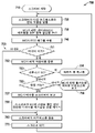
도 1은 일부 실시 예에 따른 데이터 처리 시스템을 블록도 형태로 도시한다.
도 2는 도 1의 데이터 처리 시스템에 사용하기에 적합한 가속 처리 유닛(APU, accelerated processing unit)을 블록도 형태로 도시한다.
도 3은 일부 실시 예에 따른 도 2의 APU에 사용하기에 적합한 메모리 제어기 및 관련 물리적 인터페이스(PHY)를 블록도 형태로 도시한다.
도 4는 일부 실시 예에 따른 도 2의 APU에 사용하기에 적합한 다른 메모리 제어기 및 관련 PHY를 블록도 형태로 도시한다.
도 5는 일부 실시 예에 따른 메모리 제어기를 블록도 형태로 도시한다.
도 6은 일부 실시 예에 따른 통합 패키지 후 복구 기능을 갖는 데이터 처리 시스템을 블록도 형태로 도시한다.
도 7은 일부 실시 예에 따른 도 6의 데이터 처리 시스템에서의 패키지 후 복구에 관련된 동작들의 흐름도를 도시한다.
도 8은 일부 실시 예에 따른 패키지 후 복구 루틴의 흐름도를 도시한다.
다음 설명에서, 상이한 도면들에서 동일한 참조 부호들을 사용하는 것은 유사하거나 동일한 항목들을 나타낸다. 달리 언급되지 않는 한, 단어 "결합된(coupled)"및 이와 관련된 동사 형태들은 당업계에 공지된 수단에 의한 직접적인 연결 및 간접적인 전기적 연결 양자를 포함하고, 달리 언급되지 않는 한 직접 연결에 대한 모든 설명은 또한 간접적인 전기적 연결의 적절한 형태들을 사용하는 대안적인 실시예들을 암시한다. 1 illustrates a data processing system in block diagram form in accordance with some embodiments.
FIG. 2 shows in block diagram form an accelerated processing unit (APU) suitable for use in the data processing system of FIG. 1 ;
3 illustrates in block diagram form a memory controller and associated physical interface (PHY) suitable for use with the APU of FIG. 2 in accordance with some embodiments.
4 illustrates, in block diagram form, another memory controller and associated PHY suitable for use in the APU of FIG. 2 in accordance with some embodiments.
5 illustrates a memory controller in block diagram form in accordance with some embodiments.
6 illustrates, in block diagram form, a data processing system having a post-integration package recovery function in accordance with some embodiments.
7 illustrates a flowchart of operations related to post-package recovery in the data processing system of FIG. 6 in accordance with some embodiments.
8 depicts a flow diagram of a post-package recovery routine in accordance with some embodiments.
In the following description, the use of the same reference signs in different drawings indicates similar or identical items. Unless stated otherwise, the word "coupled" and related verb forms include both direct and indirect electrical connections by means known in the art, and unless otherwise stated, all references to direct connection are included. The description also suggests alternative embodiments using suitable forms of indirect electrical connection.
하기에서 하나의 형태로 설명되는 바와 같이, 패키지 후 복구 시스템은 메모리 채널 제어기, 스크러버, 제1 에러 카운터 및 데이터 프로세서를 포함한다. 메모리 채널 제어기는 호스트 인터페이스로부터 수신되는 데이터 액세스 요청들을 메모리 인터페이스에 제공되는 대응하는 메모리 액세스들로 변환하고, 메모리 인터페이스로부터 수신되는 응답들에 응답하여 호스트 인터페이스로 리턴된 데이터를 제공하며, 응답들은 리턴된 데이터 및 복수의 에러 정정 코드(ECC, error correcting code) 비트를 포함한다. 제1 에러 카운터는 메모리 채널 제어기에 결합되고 리턴된 데이터의 에러들을 카운팅하며, 미리 결정된 상태에 도달하는 것에 응답하여 제어 신호를 제공한다. 스크러버는 메모리 채널 제어기에 결합되어 메모리 시스템의 복수의 어드레스로부터 순차적으로 그리고 주기적으로 데이터를 판독하도록, 그리고 정정 가능한 에러를 검출하는 것에 응답하여, 정정된 데이터를 재기입하도록 메모리 채널 제어기를 제어한다. 데이터 프로세서는 메모리 채널 제어기에 결합되고 제어 신호에 응답하여 메모리 시스템과 함께 패키지 후 복구 동작을 수행하기 위한 제어 신호에 반응한다.As described in one form below, the post-package recovery system includes a memory channel controller, a scrubber, a first error counter and a data processor. The memory channel controller converts data access requests received from the host interface into corresponding memory accesses provided to the memory interface, and provides data returned to the host interface in response to responses received from the memory interface, the responses being returned. data and a plurality of error correcting code (ECC) bits. A first error counter is coupled to the memory channel controller and counts errors in the returned data and provides a control signal in response to reaching a predetermined state. The scrubber is coupled to the memory channel controller to control the memory channel controller to sequentially and periodically read data from a plurality of addresses in the memory system and to write corrected data back in response to detecting a correctable error. The data processor is coupled to the memory channel controller and responsive to the control signal for performing a post-package recovery operation with the memory system in response to the control signal.
다른 형태로, 메모리 제어기는 메모리 시스템 상에서 패키지 후 복구를 수행하는 시스템에 사용하기에 적합하다. 메모리 제어기는 메모리 채널 제어기 및 제1 에러 카운터를 포함한다. 메모리 채널 제어기는 호스트 인터페이스로부터 수신되는 데이터 액세스 요청들을 메모리 인터페이스 상의 대응하는 메모리 액세스들로 변환하고, 메모리 인터페이스로부터 수신되는 응답들에 응답하여 호스트 인터페이스로 리턴된 데이터를 제공한다. 응답들은 리턴된 데이터 및 복수의 에러 정정 코드(ECC) 비트를 포함한다. 메모리 채널 제어기는 리턴된 데이터에 대응하는 복수의 에러 정정 코드(ECC) 비트에 기초하여 에러 검사를 수행함으로써 리턴된 데이터의 에러를 검출하고, 리턴된 데이터의 에러를 검출하는 것 응답하여 카운트 신호를 제공한다. 제1 에러 카운터는 메모리 채널 제어기에 결합되어 카운트 신호에 응답하여 에러들을 카운팅하고, 미리 결정된 상태에 도달하는 것에 응답하여, 제어 신호, 예를 들어 기계 검사 아키텍처(MCA, machine check architecture) 예외를 제공한다. MCA 예외는 패키지 후 복구 펌웨어를 실행하는 데이터 프로세서와 같은 다른 에이전트가 패키지 후 복구 동작을 수행하게 한다.In another form, the memory controller is suitable for use in a system that performs post-package recovery on a memory system. The memory controller includes a memory channel controller and a first error counter. The memory channel controller converts data access requests received from the host interface into corresponding memory accesses on the memory interface, and provides data returned to the host interface in response to responses received from the memory interface. The responses include returned data and a plurality of error correction code (ECC) bits. The memory channel controller detects an error in the returned data by performing error checking based on a plurality of error correction code (ECC) bits corresponding to the returned data, and generates a count signal in response to detecting the error in the returned data. to provide. A first error counter is coupled to the memory channel controller to count errors in response to the count signal and to provide a control signal, eg, a machine check architecture (MCA) exception, in response to reaching a predetermined state do. MCA exceptions allow other agents, such as data processors running post-package recovery firmware, to perform post-package recovery operations.
또 다른 형태로, 호스트 인터페이스로부터 수신되는 데이터 액세스 요청들이 메모리 인터페이스에 제공되는 대응하는 메모리 액세스들로 변환된다. 리턴된 데이터는 메모리 인터페이스로부터 수신되는 응답들에 응답하여 호스트 인터페이스에 제공되며, 응답들은 리턴된 데이터 및 복수의 에러 정정 코드(ECC) 비트를 포함한다. 메모리 시스템은 리턴된 데이터 및 복수의 ECC 비트에 따른 에러들에 대해 스크러빙되고, 정정 가능한 에러들이 복구된다. 패키지 후 복구 동작은 스크러빙 동안 메모리 시스템의 영역에서의 미리 결정된 수의 에러에 응답하여 메모리 시스템 상에서 수행된다.In yet another form, data access requests received from a host interface are translated into corresponding memory accesses provided to the memory interface. The returned data is provided to the host interface in response to responses received from the memory interface, the responses including the returned data and a plurality of error correction code (ECC) bits. The memory system is scrubbed for errors according to the returned data and the plurality of ECC bits, and correctable errors are recovered. A post-package recovery operation is performed on the memory system in response to a predetermined number of errors in an area of the memory system during scrubbing.
도 1은 일부 실시 예에 따른 데이터 처리 시스템(100)을 블록도 형태로 도시한다. 데이터 처리 시스템(100)은 일반적으로 가속 처리 유닛(APU) 형태의 데이터 프로세서(110), 메모리 시스템(120), 주변 장치 상호 연결 익스프레스(PCIe) 시스템(150), 범용 직렬 버스(USB) 시스템(160) 및 디스크 드라이브(170)를 포함한다. 데이터 프로세서(110)는 데이터 처리 시스템(100)의 중앙 처리 유닛(CPU)으로서 작동하고 최신 컴퓨터 시스템들에 유용한 다양한 버스 및 인터페이스를 제공한다. 이러한 인터페이스들에는 두 개의 DDRx(double data rate) 메모리 채널, PCIe 링크 연결용 PCIe 루트 컴플렉스, USB 네트워크 연결용 USB 제어기 및 SATA(Serial Advanced Technology Attachment) 대용량 저장 장치에 대한 인터페이스가 포함된다.1 illustrates a
메모리 시스템(120)은 메모리 채널(130) 및 메모리 채널(140)을 포함한다. 메모리 채널(130)은 본 예에서는 별도의 랭크들에 대응하는 대표적인 듀얼 인라인 메모리 모듈들(DIMMs)(134, 136 및 138)을 포함하여, DDRx 버스(132)에 연결되는 DIMM 세트를 포함한다. 마찬가지로, 메모리 채널(140)은 대표적인 DIMM들(144, 146 및 148)을 포함하여, DDRx 버스(142)에 연결된 DIMM 세트를 포함한다.The
PCIe 시스템(150)은 데이터 프로세서(110) 내의 PCIe 루트 컴플렉스에 연결되는 PCIe 스위치(152), PCIe 장치(154), PCIe 장치(156) 및 PCIe 장치(158)를 포함한다. PCIe 장치(156)는 차례로 시스템 기본 입/출력 시스템(BIOS) 메모리(157)에 연결된다. 시스템 BIOS 메모리(157)는 ROM(read-only memory), 플래시 EEPROM(electrically erasable programmable ROM) 등과 같은 다양한 비 휘발성 메모리 유형 중 임의의 것일 수 있다.
USB 시스템(160)은 데이터 프로세서(110) 내의 USB 마스터에 연결되는 USB 허브(162), 및 USB 허브(162)에 각각 연결되는 대표적인 USB 장치들(164, 166 및 168)을 포함한다. USB 장치들(164, 166 및 168)은 키보드, 마우스, 플래시 EEPROM 포트 등과 같은 장치들일 수 있다.
디스크 드라이브(170)는 SATA 버스를 통해 데이터 프로세서(110)에 연결되고 운영 체제, 애플리케이션 프로그램들, 애플리케이션 파일들 등을 위한 대용량 저장 장치를 제공한다.The
데이터 처리 시스템(100)은 메모리 채널(130) 및 메모리 채널(140)을 제공함으로써 최신 컴퓨팅 애플리케이션들에 사용하기에 적합하다. 메모리 채널들(130 및 140) 각각은 DDR 버전 4(DDR4), 저전력 DDR4(LPDDR4), 그래픽스 DDR 버전 5(gDDR5) 및 고대역폭 메모리(HBM)와 같은 최첨단 DDR 메모리들에 연결할 수 있고, 장차 메모리 기술들에 적용될 수 있다. 이러한 메모리들은 높은 버스 대역폭 및 고속 동작을 제공한다. 동시에, 그것들은 또한 랩톱 컴퓨터들과 같은 배터리 구동 애플리케이션들의 전력을 절감하기 위해 저전력 모드들을 제공하고, 내장된 열 모니터링 기능도 제공한다.The
도 2는 도 1의 데이터 처리 시스템(100)에 사용하기에 적합한 APU(200)를 블록도 형태로 도시한다. APU(200)는 일반적으로 중앙 처리 유닛(CPU) 코어 컴플렉스(210), 그래픽스 코어(220), 디스플레이 엔진 세트(230), 메모리 관리 허브(240), 데이터 패브릭(250), 주변 제어기 세트(260), 주변 버스 제어기 세트(270), 시스템 관리 유닛(SMU)(280), 및 메모리 제어기 세트(290)를 포함한다.FIG. 2 illustrates in block diagram form an
CPU 코어 컴플렉스(210)는 CPU 코어(212) 및 CPU 코어(214)를 포함한다. 이러한 예에서, CPU 코어 컴플렉스(210)는 두 개의 CPU 코어를 포함하지만, 다른 실시 예들에서는 CPU 코어 컴플렉스가 임의의 수의 CPU 코어를 포함할 수 있다. CPU 코어들(212 및 214) 각각은 제어 패브릭을 형성하는 시스템 관리 네트워크(SMN)에 그리고 데이터 패브릭(250)에 양방향으로 연결되고, 데이터 패브릭(250)에 메모리 액세스 요청들을 제공할 수 있다. CPU 코어들(212 및 214) 각각은 단일 코어들일 수 있거나, 또한 캐시들과 같은 특정 자원들을 공유하는 두 개 이상의 단일 코어를 갖는 코어 컴플렉스일 수 있다.The
그래픽스 코어(220)는 고집적 병렬 방식으로 버텍스 프로세싱, 프래그먼트 프로세싱, 쉐이딩(shading), 텍스쳐 블렌딩(text blending) 등과 같은 그래픽 동작들을 수행할 수 있는 고성능 그래픽 처리 유닛(GPU)이다. 그래픽스 코어(220)는 SMN에 그리고 데이터 패브릭(250)에 양방향으로 연결되고, 데이터 패브릭(250)에 메모리 액세스 요청들을 제공할 수 있다. 이와 관련하여, APU(200)는 CPU 코어 컴플렉스(210) 및 그래픽스 코어(220)가 동일한 메모리 공간을 공유하는 일원화된 메모리 아키텍처, 또는 CPU 코어 컴플렉스(210) 및 그래픽스 코어(220)가 메모리 공간의 일 부분을 공유하는 메모리 아키텍처를 지원할 수 있는 한편, 그래픽스 코어(220)는 또한 CPU 코어 컴플렉스(210)가 액세스할 수 없는 개인 그래픽스 메모리를 사용한다.The
디스플레이 엔진(230)은 그래픽스 코어(220)에 의해 생성된 객체들을 렌더링 및 래스터화하여 모니터 상에 디스플레이한다. 그래픽스 코어(220) 및 디스플레이 엔진들(230)은 메모리 시스템(120)에서의 적절한 어드레스로 균일한 변환을 위해 공통 메모리 관리 허브(240)에 양방향으로 연결되고, 메모리 관리 허브(240)는 그러한 메모리 액세스를 발생시키고 메모리 시스템으로부터 리턴되는 판독 데이터를 수신하기 위해 데이터 패브릭(250)에 양방향으로 연결된다.The
데이터 패브릭(250)은 임의의 메모리 액세싱 에이전트와 메모리 제어기들(290) 사이에서 메모리 액세스 요청들 및 메모리 응답들을 라우팅하기 위한 크로스바 스위치를 포함한다. 그것은 또한 시스템 구성을 기반으로 메모리 액세스 대상들, 뿐만 아니라 각 가상 연결을 위한 버퍼들을 결정하기 위한, BIOS에 의해 정의되는 시스템 메모리 맵도 포함한다.
주변 제어기들(260)은 각각이 시스템 허브(266) 및 SMN 버스에 양방향으로 연결되는 USB 제어기(262) 및 SATA 인터페이스 제어기(264)를 포함한다. 이러한 두 개의 제어기는 APU(200)에 사용될 수 있는 주변 제어기들의 단지 예시적인 것이다.
주변 버스 제어기들(270)은 각각이 입/출력(I/O) 허브(276)에 그리고 SMN 버스에 양방향으로 연결되는 "사우스브리지"(SB, Southbridge)(272) 및 PCIe 제어기(274) 또는 시스템 제어기를 포함한다. I/O 허브(276)는 또한 시스템 허브(266) 및 데이터 패브릭(250)에 양방향으로 연결된다. 그에 따라 예를 들어 CPU 코어는 데이터 패브릭(250)이 I/O 허브(276)를 통해 라우팅하는 액세스를 통해 USB 제어기(262), SATA 인터페이스 제어기(264), SB(272) 또는 PCIe 제어기(274)에 레지스터들을 프로그램할 수 있다.
SMU(280)는 APU(200)상의 자원들의 동작을 제어하고 이들 사이의 통신을 동기화하는 로컬 제어기이다. SMU(280)는 APU(200)상의 다양한 프로세서의 작동 시작 시퀀싱을 관리하고, 리셋, 인에이블 및 다른 신호들을 통해 다수의 오프-칩 장치를 제어한다. SMU(280)는 APU(200)의 각 구성요소들에 클록 신호들을 제공하기 위해, 위상 동기 루프(PLL)와 같은 하나 이상의 클록 공급원(도 2에 도시되지 않음)을 포함한다. 또한 SMU(280)는 다양한 프로세서 및 다른 기능 블록을 위한 전력을 관리하고, 적절한 전력 상태들을 결정하기 위해 CPU 코어들(212 및 214) 및 그래픽스 코어(220)로부터 측정된 전력 소모 값들을 수신할 수 있다.
또한, APU 200은 다양한 시스템 모니터링 및 절전 기능을 구현한다. 특히 하나의 시스템 모니터링 기능은 열 모니터링이다. 예를 들어, APU(200)가 뜨거워지면, SMU(280)가 CPU 코어들(212 및 214) 및/또는 그래픽스 코어(220)의 주파수 및 전압을 감소시킬 수 있다. APU(200)가 너무 뜨거워지면, 그것이 완전히 종료될 수 있다. 또한 열 이벤트들은 SMU(280)에 의해 외부 센서들로부터 SMN 버스를 통해 수신될 수 있고, SMU(280)는 이에 응답하여 클록 주파수 및/또는 전원 전압을 감소시킬 수 있다.In addition, the
도 3은 일부 실시 예에 따른 도 2의 APU(200)에 사용하기에 적합한 메모리 제어기(300) 및 관련 물리적 인터페이스(PHY)(330)를 블록도 형태로 도시한다. 메모리 제어기(300)는 메모리 채널(310) 및 전력 엔진(320)을 포함한다. 메모리 채널(310)은 호스트 인터페이스(312), 메모리 채널 제어기(314) 및 물리적 인터페이스(316)를 포함한다. 호스트 인터페이스(312)는 가변형 데이터 포트(SDP, scalable data port)를 통해 메모리 채널 제어기(314)를 데이터 패브릭(250)에 양방향으로 연결한다. 물리적 인터페이스(316)는 DDR-PHY 인터페이스 사향(DFI)을 따르는 버스를 통해 메모리 채널 제어기(314)를 PHY(330)에 양방향으로 연결한다. 전력 엔진(320)은 SMN 버스를 통해 SMU(280)에, APB(Advanced Peripheral Bus)를 통해 PHY(330)에 양방향으로 연결되고, 또한 메모리 채널 제어기(314)에 양방향으로 연결된다. PHY(330)는 도 1의 메모리 채널(130) 또는 메모리 채널(140)과 같은 메모리 채널에 대한 양방향 연결을 갖는다. 메모리 제어기(300)는 단일 메모리 채널 제어기(314)를 사용하는 단일 메모리 채널에 대한 메모리 제어기의 예시이고, 하기에서 더 설명될 방식으로 메모리 채널 제어기(314)의 동작을 제어하는 전력 엔진(320)을 갖는다.3 illustrates in block diagram form a
도 4는 일부 실시 예에 따른 도 2의 APU(200)에 사용하기에 적합한 다른 메모리 제어기(400) 및 관련 PHY들(440 및 450)을 블록도 형태로 도시한다. 메모리 제어기(400)는 메모리 채널들(410 및 420) 및 전력 엔진(430)을 포함한다. 메모리 채널(410)은 호스트 인터페이스(412), 메모리 채널 제어기(414) 및 물리적 인터페이스(416)를 포함한다. 호스트 인터페이스(412)는 메모리 채널 제어기(414)를 SDP를 통해 데이터 패브릭(250)에 양방향으로 연결한다. 물리적 인터페이스(416)는 메모리 채널 제어기(414)를 PHY(440)에 양방향으로 연결하고, DFI 사양을 따른다. 메모리 채널(420)은 호스트 인터페이스(422), 메모리 채널 제어기(424) 및 물리적 인터페이스(426)를 포함한다. 호스트 인터페이스(422)는 다른 SDP를 통해 메모리 채널 제어기(424)를 데이터 패브릭(250)에 양방향으로 연결한다. 물리적 인터페이스(426)는 메모리 채널 제어기(424)를 PHY(450)에 양방향으로 연결하고, DFI 사양을 따른다. 전력 엔진(430)은 SMN 버스를 통해 SMU(280)에, APB를 통해 PHY들(440 및 450)에 양방향으로 연결되고, 또한 메모리 채널 제어기들(414 및 424)에 양방향으로 연결된다. PHY(440)는 도 1의 메모리 채널(130)과 같은 메모리 채널에 대한 양방향 연결을 갖는다. PHY(450)는 도 1의 메모리 채널(140)과 같은 메모리 채널에 대한 양방향 연결을 갖는다. 메모리 제어기(400)는 두 개의 메모리 채널 제어기를 갖는 메모리 제어기의 예시이고, 하기에 더 설명될 방식으로 메모리 제어기(414) 및 메모리 채널 제어기(424) 양자의 동작을 제어하기 위해 공유 전력 엔진(430)을 사용한다.4 illustrates, in block diagram form, another
도 5는 일부 실시 예에 따른 메모리 제어기(500)를 블록도 형태로 도시한다. 메모리 제어기(500)는 일반적으로 메모리 채널 제어기(510) 및 전력 제어기(550)를 포함한다. 메모리 채널 제어기(510)는 일반적으로 인터페이스(512), 큐(514), 명령 큐(520), 어드레스 생성기(522), 내용 주소 화 메모리(CAM, content addressable memory)(524), 재생 큐(replay queue)(530), 복원 논리 블록(refresh logic block)(532), 타이밍 블록(534), 페이지 테이블(536), 아비터(arbiter)(538), 에러 정정 코드(ECC) 체크 블록(542), ECC 생성 블록(544) 및 데이터 버퍼(DB)(546)를 포함한다.5 illustrates a
인터페이스(512)는 외부 버스를 통해 데이터 패브릭(250)에 대한 제1 양방향 연결을 갖고, 출력을 갖는다. 메모리 제어기(500)에서, 이러한 외부 버스는 "AXI4"로 알려진 영국의 캠브리지(Cambridge) 소재의 ARM 홀딩스(ARM Holdings), PLC에 의해 명시된 고급 확장형 인터페이스 버전 4와 호환 가능하지만, 다른 실시 예들에서는 인터페이스들의 다른 유형들일 수 있다. 인터페이스(512)는 메모리 액세스 요청들을 FCLK(또는 MEMCLK) 도메인으로 알려진 제1 클록 도메인으로부터 UCLK 도메인으로 알려진 메모리 제어기(500) 내부의 제2 클록 도메인으로 변환한다. 유사하게, 큐(514)는 UCLK 도메인으로부터 DFI 인터페이스와 연관된 DFICLK 도메인으로의 메모리 액세스를 제공한다.
어드레스 생성기(522)는 AXI4 버스를 통해 데이터 패브릭(250)으로부터 수신된 메모리 액세스 요청들의 어드레스들을 디코딩한다. 메모리 액세스 요청들은 정규화된 포맷으로 표현된 물리적 어드레스 공간에서의 액세스 어드레스들을 포함한다. 어드레스 생성기(522)는 정규화된 어드레스를 메모리 시스템(120) 내의 실제 메모리 장치들을 어드레싱할 뿐만 아니라, 관련 액세스를 효율적으로 스케줄링하는 데 사용될 수 있는 포맷으로 변환한다. 이러한 포맷에는 메모리 액세스 요청을 특정 랭크, 로우 어드레스, 컬럼 어드레스 , 뱅크 어드레스 및 뱅크 그룹과 연관시키는 영역 식별자가 포함된다. 시작 시, 시스템 바이오스는 그것들의 크기 및 구성을 결정하기 위해 메모리 시스템(120) 내의 메모리 장치들에 질의하고, 어드레스 생성기(522)와 연관된 구성 레지스터 세트를 프로그램한다. 어드레스 생성기(522)는 구성 레지스터들에 저장된 구성을 사용하여 정규화된 어드레스를 적절한 포맷으로 변환한다. 명령 큐(520)는 CPU 코어들(212 및 214) 및 그래픽스 코어(220)와 같은 데이터 처리 시스템(100)에서의 메모리 액세싱 에이전트들로부터 수신되는 메모리 액세스 요청들의 큐이다. 명령 큐(520)는 어드레스 생성기(522)에 의해 디코딩된 어드레스 필드들뿐만 아니라, 액세스 유형 및 서비스 품질(QoS) 식별자들을 포함하여, 아비터(538)가 메모리 액세스를 효율적으로 선택할 수 있게 하는 다른 어드레스 정보를 저장한다. CAM(524)은 기입 후 기입(WAW, write after write) 및 판독 후 기입(RAW, read after write) 순서 규칙들과 같은 순서 규칙들을 시행하기 위한 정보를 포함한다.
재생 큐(530)는 어드레스 및 명령 패리티 응답, DDR4 DRAM에 대한 기입 순환 중복 검사(CRC, cyclic redundancy check) 응답들 또는 gDDR5 DRAM에 대한 기입 및 판독 CRC 응답들과 같은 응답들을 대기하는 아비터(538)에 의해 선택된 메모리 액세스를 저장하기 위한 임시 큐이다. 재생 큐(530)는 ECC 체크 블록(542)에 액세스하여 리턴된 ECC가 정확한지 또는 에러를 나타내는지를 결정한다. 재생 큐(530)는 이러한 사이클들 중 하나의 패리티 또는 CRC 에러의 경우에 액세스가 재생되게 한다.The
복원 로직(532)은 메모리 액세싱 에이전트들로부터 수신된 정상적인 판독 및 기입 메모리 액세스 요청들과는 별도로 생성되는 다양한 전원 차단, 복원 및 종결 저항(ZQ, termination resistance) 캘리브레이션 사이클들을 위한 상태 기계들을 포함한다. 예를 들어, 메모리 랭크가 선충전 전원 차단에 있으면, 그것은 복원 사이클들을 실행하기 위해 주기적으로 재개되어야 한다. 복원 로직(532)은 주기적으로 복원 명령들을 생성하여 DRAM 칩들 내의 메모리 셀들의 저장 커패시터들로부터 전하가 누설됨으로써 야기되는 데이터 에러들을 방지한다. 또한, 복원 로직(532)은 시스템의 열 변화로 인한 온-다이 종결 저항의 불일치를 방지하기 위해 ZQ를 주기적으로 캘리브레이션한다.Restore
아비터(538)는 명령 큐(520)에 양방향으로 연결되고 메모리 채널 제어기(510)의 핵심이다. 메모리 버스의 사용량을 개선하기 위해 액세스를 지능적으로 스케줄링함으로써 효율성을 향상시킨다. 아비터(538)는 타이밍 블록(534)을 사용하여 명령 큐(520) 내의 특정 액세스가 DRAM 타이밍 파라미터들에 기초하여 발행에 적합한지 여부를 결정함으로써 적절한 타이밍 관계들을 강화한다. 예를 들어, 각 DRAM은 "tRC"라고 알려져 있는 활성화 명령들 간 최소 지정 시간을 갖는다. 타이밍 블록(534)은 이러한 그리고 JEDEC 사양에 명시된 다른 타이밍 파라미터들에 기초하여 적합성을 결정하는 카운터 세트를 유지하고, 재생 큐(530)에 양방향으로 연결된다. 페이지 테이블(536)은 아비터(538)에 대한 메모리 채널의 각 뱅크 및 랭크에 활성 페이지들에 관한 상태 정보를 유지하고, 재생 큐(530)에 양방향으로 연결된다.
인터페이스(512)로부터 수신되는 기입 메모리 액세스 요청들에 응답하여, ECC 생성 블록(544)은 기입 데이터에 따른 ECC를 계산한다. DB(546)는 수신된 메모리 액세스 요청들에 대한 기록 데이터 및 ECC를 저장한다. 그것은 아비터(538)가 메모리 채널로의 디스패치(dispatch)를 위해 대응하는 기입 액세스를 선택할 때 조합된 기입 데이터/ECC를 큐(514)로 출력한다.In response to write memory access requests received from the
전력 제어기(550)는 일반적으로 고급 확장향 인터페이스, 버전 1(AXI), APB 인터페이스(554) 및 전력 엔진(560)에 대한 인터페이스(552)를 포함한다. 인터페이스(552)는 SMN에 대한 제1 양방향 연결을 가지며, 이는 도 5에 별도로 도시된 "EVENT_n"으로 라벨링된 이벤트 신호를 수신하기 위한 입력, 그리고 출력을 포함한다. APB 인터페이스(554)는 인터페이스(552)의 출력에 연결되는 입력, 및 APB를 통해 PHY에 연결하기 위한 출력을 갖는다. 전력 엔진(560)은 인터페이스(552)의 출력에 연결되는 입력, 및 큐(514)의 입력에 연결되는 출력을 갖는다. 전력 엔진(560)은 구성 레지스터 세트(562), 마이크로 제어기(μC)(564), 자기 복원 제어기(SLFREF/PE)(566) 및 신뢰 판독/기입 타이밍 엔진(RRW/TE)(568)을 포함한다. 구성 레지스터(562)는 AXI 버스를 통해 프로그램되고, 메모리 제어기(500) 내의 다양한 블록의 동작을 제어하기 위한 구성 정보를 저장한다. 그에 따라, 구성 레지스터들(562)은 도 5에 상세히 도시되지 않은 이러한 블록들에 연결되는 출력들을 갖는다. 자기 복원 제어기(566)는 복원 로직(532)에 의한 복원의 자동 발생에 더하여 복원의 수동 발생을 가능하게 하는 엔진이다. 신뢰 판독/기입 타이밍 엔진(568)은 DDR 인터페이스 최대 판독 지연(MRL, maximum read latency) 트레이닝 및 루프백 테스트와 같은 목적들을 위해 메모리 또는 I/O 장치들에 연속적인 메모리 액세스 스트림을 제공한다.The
메모리 채널 제어기(510)는 그것이 관련 메모리 채널로의 디스패치를 위해 메모리 액세스를 선택하게하는 회로를 포함한다. 바람직한 중재 결정을 내리기 위해, 어드레스 생성기(522)는 어드레스 정보를 메모리 시스템에서의 랭크, 로우 어드레스, 컬럼 어드레스, 뱅크 어드레스 및 뱅크 그룹을 포함하는 사전 디코딩 정보로 디코딩하고, 명령 큐(520)는 사전 디코딩 정보를 저장한다. 구성 레지스터(562)는 어드레스 생성기(522)가 수신된 어드레스 정보를 어떻게 디코딩 하는지를 결정하기위한 구성 정보를 저장한다. 아비터(538)는 디코딩된 어드레스 정보, 타이밍 블록(534)에 의해 지시된 타이밍 적격 정보, 및 페이지 테이블(536)에 의해 표시된 활성 페이지 정보를 사용하여 QoS 요건과 같은 다른 기준을 관찰하면서 메모리 액세스를 효율적으로 스케줄링한다. 예를 들어, 아비터(538)는 메모리 페이지들을 변경하는 데 필요한 선충전 및 활성화 명령들의 오버헤드를 회피하기 위해 개방 페이지들에의 액세스에 대한 선호도를 구현하고, 그것들을 다른 뱅크에의 판독 및 기입 액세스와 인터리빙함으로써 하나의 뱅크에의 오버헤드 액세스를 감춘다. 특히, 정상 동작 동안, 아비터(538)는 정상적으로 페이지들을 상이한 페이지를 선택하기 전에 그것들이 선충전되어야 할 때까지 상이한 뱅크들에 개방 상태로 유지한다.
도 6은 일부 실시 예에 따른 통합 패키지 후 복구 기능을 갖는 데이터 처리 시스템(600)을 블록도 형태로 도시한다. 데이터 처리 시스템(600)은 일반적으로 데이터 프로세서(610), 데이터 패브릭(620), 메모리 제어기(630), PHY(660) 및 메모리 시스템(670)을 포함한다. 데이터 프로세서(610)는 패키지 후 복구 펌웨어 및 CPU 코어(614)를 저장하는 메모리(612)를 포함한다. 메모리(612)는 도 1의 시스템 바이오스(157)에 대응하는 반면, CPU 코어(614)는 CPU 코어(212) 또는 CPU 코어(214)와 같은 CPU 코어 컴플렉스(210)의 CPU 코어에 대응한다. 도 1의 멀티 코어 아키텍처에서, CPU 코어들 중 하나는 바이오스 서비스 프로세서(BSP)로 알려져 있고 시스템 바이오스(157)에 연결된다. 데이터 프로세서(610)에서, CPU 코어(614)는 BSP이고 패키지 후 복구 펌웨어를 포함하여 바이오스 명령들을 판독하고 실행하기 위해 메모리(612)에 양방향으로 연결된다. 또한 CPU 코어(614)는 메모리 시스템에 판독 및 기록 명령들을 발행하고 메모리 시스템으로부터 판독 응답들을 수신하기 위해, 그리고 CPU 코어들 중 하나의 내부 캐시에 저장될 수 있는 공유 데이터에 대해 자신과 다른 CPU 코어 컴플렉스들 사이에서 프로브들을 발행 및 응답하기 위해 데이터 패브릭(620)에 양방향으로 연결된다.6 illustrates, in block diagram form, a
데이터 패브릭(620)은 코히런트 슬레이브(622) 및 제어 블록(626)을 포함한다. 코히런트 슬레이브(622)는 액세스를 생성하고 메모리 제어기(630)와 같은 적절한 메모리 제어기에 액세스를 제공하기 위한 판독 및 기입 요청들에 응답하는 엔진이다. 또한 코히런트 슬레이브(622)는 스크러버(624)를 포함한다. 스크러버(624)는 시스템 내의 각 메모리 칩의 각 뱅크 및 메모리 칩들의 각 랭크를 포함하여, 메모리에서의 각 위치에 대한 메모리 어드레스들을 통해 순환함으로써 스크러빙 동작을 수행하는데 사용되는 하드웨어 상태 기계이다. 스크러빙 동작 시, 코히런트 슬레이브(622)는 메모리 에러들이 검출될 수 있고 몇몇 에러는 정정될 수 있도록 메모리 시스템(670)에서의 연속적인 위치에 판독-수정-기입 사이클들을 발행한다. 다른 한편, 제어 블록(626)은 보고된 에러들을 추적하고, 정정 불가능한 메모리 에러들에 대한 기계 검사 인터럽트(machine check interrupt)를 시그널링한다. 또한 제어 블록(626)은 메모리(612)에 저장된 패키지 후 복구를 사용하여 패키지 후 복구 동작을 수행할 필요성을 CPU 코어(614)에 시그널링한다.The
메모리 제어기(630)는 도 5의 메모리 제어기(500)를 사용하여 구현될 수 있다. 그러나 도 6에 도시된 메모리 제어기(630)는 메모리 에러 검출, 정정, 및 패키지 후 복구 결정을 구현하는 데 사용되는 메모리 제어기의 부분들만을 포함한다. 도시된 바와 같이 메모리 제어기(630)는 메모리 채널 제어기(640) 및 전력 엔진(650)을 포함한다. 메모리 채널 제어기(640)는 호스트 인터페이스(642), PHY 인터페이스(644), 내부 데이터 경로(646) 및 ECC 검사 회로(648)를 포함한다. 내부 데이터 경로(646)는 데이터 및 ECC 신호들을 전달하는데 사용되고 호스트 인터페이스(642), PHY 인터페이스(644) 및 ECC 검사 회로(648)를 내부적으로 연결한다. 호스트 인터페이스(642)는 AXI4 버스에 연결되는 양방향 포트 및 내부 데이터 경로(646)에 연결하기 위한 양방향 포트를 갖는다. PHY 인터페이스(644)는 내부 데이터 경로(646)에 연결되는 양방향 포트 및 DFI 버스에 연결하기 위한 양방향 포트를 갖는다. ECC 검사 회로(648)는 내부 데이터 경로(646)에 연결되는 양방향 포트 및 여덟 개의 출력 세트(도 6은 각각 랭크 0 및 랭크 7에 대응하는 "INC_CS0" 및 "INC_CS7"로 라벨링된 두 개의 대표적인 출력을 도시한다)를 갖는다. 전력 엔진(650)은 각각 랭크 0 및 랭크 7에 대응하는 각각의 신호들(INC_CS0 및 INC_CS7)을 수신하는 대표적인 카운터들(652 및 654)을 포함하여 여덟 개의 카운터 세트를 포함한다. 각각의 카운터는 데이터 패브릭(620)에서의 제어 블록(626)에 AXI 버스를 통해 카운터 오버플로우 신호를 제공하기 위한 출력을 갖는다.The
PHY(660)는 DFI 버스를 통해 메모리 제어기(630)에 연결되는 양방향 포트, 및 메모리 시스템(670)에 연결하기 위한 "DDR4 인터페이스"로 라벨링된 메모리 인터페이스에 연결되는 양방향 포트를 갖는다. PHY(660)는 도 3의 DDRx PHY(330) 뿐만 아니라 도 5의 DDRx PHY들(440 및 450)에 관하여 전술한 바와 같이 구현될 수 있다.
메모리 시스템(670)은 DDR4 메모리 시스템이고 DDR4 인터페이스를 통해 PHY(660)에 연결된다. DDR4 메모리는 패키지 후 복구를 지원하고 그에 따라 하기에서 더 상세히 설명될 방식으로 데이터 처리 시스템(600)과 상호 작용한다.
동작 시, 데이터 처리 시스템(600)은 가용 자원들을 사용하여 메모리 신뢰성 검사, 정정 가능한 ECC 에러들의 복구, 정정 불가능한 ECC 에러들의 보고, 그리고 패키지 후 복구를 효율적으로 수행한다. 또한 그것은 백그라운드 스크러빙 동작들을 활용하여 하드 에러들을 검출하고 정정 불가능한 에러들이 발생하기 전에 DDR4 DRAM들과 같은 일부 DRAM의 패키지 후 복구 기능을 사용하여 그것들을 정정한다.In operation,
데이터 처리 시스템(600)은 데이터 프로세서(610), 데이터 패브릭(620) 및 메모리 제어기(630) 사이에 패키지 후 검출 및 정정 작업을 효율적으로 분배한다. 데이터 패브릭(620)은 메모리 시스템(670)에서의 모든 메모리 위치의 백그라운드 스크러빙을 수행하는 스크러버(624)를 포함한다. 스크러빙은 저대역폭 백그라운드 동작이기 때문에, 단일 스크러버를 다수의 메모리 제어기와 함께 사용하여 단지 소량의 회로 면적으로 전체 메모리 공간을 스크러빙할 수 있다.
스크러버(624)는 두 개의 동작 모드를 갖는다. 첫째, 백그라운드 스크러빙을 수행하는 제어 모드이다. 제어 모드에서의 백그라운드 스크러빙은 ECC 에러가 있는지 여부를 결정하기 위해 각 메모리 위치를 판독하는 것을 수반한다. 특정 메모리 위치에 대한 ECC 에러가 없다면, 스크러버(624)는 메모리 공간에서 계속해서 후속 메모리 위치를 판독하기 전에 데이터를 재기입한다. 일 실시 예에서, 스크러버(624)는 일부 DRAM이 온-칩 ECC를 구현하기 때문에 정정 가능한 ECC 에러가 검출되었는지 여부에 관계없이 데이터를 재기입하고, 후속 기입 사이클은 DRAM에서 검출되었지만 정정됨에 따라 스크러버(624)에 보이지 않는 정정 가능한 ECC 에러가 업데이트된 데이터가 페이지 버퍼에 재기입하게 할 것임을 보장한다. 그 다음 후속 선충전 명령 상에서, 정정된 데이터가 에러를 정정하기 위해 메모리 어레이에 기입될 것이다. 그러나, 후속 기입 작업이 없다면, 에러는 메모리 어레이에서 결코 정정되지 않을 것이다. 대안적인 실시 예에서, 스크러버(624)는 판독 사이클을 수행하지만 검출된 에러에 대해서만 데이터를 재기입한다. 스크러버(624)가 정정 가능한 에러를 검출하면, 에러를 기계 검사 아키텍처(MCA, machine check architecture) 예외로서 보고한다.The
스크러버(624)는 메모리 시스템(670)에서의 모든 메모리 위치를 일정 속도로 스크러빙한다. 예를 들어, 그것은 하루에 한 번 모든 메모리 위치의 스크럽을 수행하는 규칙을 따를 수 있다. 도시된 실시 예에서, 스크러버(624)는 길이 8의 버스트를 사용하는 단일 버스트에서 메모리 시스템(670)으로부터 효율적으로 판독될 수 있는, 통상적으로 64 바이트인 CPU 코어의 캐시 라인과 동일한 크기를 갖는 메모리 위치들을 판독한다. 따라서 그것은 ECC 검출 및 정정 회로뿐만 아니라 64 바이트 버퍼도 포함한다. 그러나 다른 실시 예들에서 스크러버(624)는 영역 또는 페이지와 같은 다양한 다른 크기의 메모리 위치들을 판독할 수 있다.The
둘째, 스크러버(624)는 재지시 모드를 갖는다. 전술한 바와 같이, 시스템 ECC 에러가 발생한 시스템 액세스에 응답하여, 스크러버(624)는 시스템 바이오스에 에러를 보고한다. 예를 들어, DDRx DIMM용 공통 ECC 메커니즘은 단일 비트 에러 검출 및 정정 및 다중 비트 에러 검출을 지원한다. ECC 에러는 단일 메모리 셀의 내용을 변경하는 알파 입자로 인해 야기되었을 수 있음에 따라, 영구적으로 정정될 필요가 없는 무작위 에러를 나타낸다. 정정 가능한 ECC 에러를 보고한 것에 응답하여, 시스템 바이오스는 스크러버(624)에 메모리 위치의 판독-기입 동작을 수행할 것을 재지시한다. 그러나 스크러버(624)가 다중 비트 에러와 같은 정정 불가능한 에러를 검출하면, 스크러버는 그러한 에러를 또한 MCA 예외를 사용하여 보고하여, 데이터 프로세서(610)가 상이한 정정 조치를 취하게 한다. 예를 들어, 소프트웨어 에러 핸들러는 손상된 데이터를 사용한 소프트웨어 애플리케이션을 중지시키거나, 데이터 프로세서(610)를 리셋할 수 있다.Second, the
스크러버(624)는 각각의 판독 요청을 메모리 제어기(630)에 발행한다. 메모리 제어기(630)는 정상 동작 중재에 따라 결정된 순서로 판독 요청을 발행한다. 요청된 데이터를 수신 시, 메모리 제어기(630)는 그 자체의 ECC 검사를 수행하고 계산된 ECC가 메모리로부터 리턴된 ECC와 일치하는지 여부를 결정한다. 에러를 검출하지 않으면, 스크러버(624)는 다음 메모리 위치로 진행한다. 그러나 그것이 에러를 검출하면, 그것은 증분 신호를 활성화함으로써 전력 엔진(650)에 에러를 표시한다. 최종적으로 에러 카운트 값이 임계값을 초과하면, 카운터는 제어 블록(626)에 에러를 보고한다. 그 다음 제어 블록(626)은 패키지 후 복구 동작을 포함할 수 있는 적절한 구제책을 취한다.The
스크러버(624)를 패키지 후 복구 흐름으로 통합시킴으로써, 데이터 처리 시스템(600)은 기존의 회로 블록을 사용하여 DDR4 패키지 후 복구 기능의 성능을 해제한다. 메모리 제어기(630)에서 이용 가능한 복사 및 재기입 동작들을 사용함으로써, 그것은 대량 판독/기입 버퍼의 필요성을 회피한다. 예를 들어, 현재 메모리 구조 및 밀도에 따라, 로우는 8 킬로바이트(kB) 크기일 수 있고 이러한 유형의 동작을 판독/기입 동작들과 수행할 수 있으며 카운터는 전체 메모리 로우를 평가하는 데 8 kB 버퍼를 필요로 할 수 있다. 또한 스크러버(624)는 이미 일어나고 있는 백그라운드 작업으로서 낙제 로우로부터 데이터가 이동되도록 한다.By incorporating the
이러한 아키텍처에는 몇 가지 이점이 있다. 첫째, 아키텍처는 소프트 에러들을 검출 및 정정하는 데 이미 이용 가능할 수 있는 백그라운드 스크러빙을 활용하기 때문에 효율적이다. 둘째, 그것은 ECC 검사 회로(648) 및 카운터 세트와 같은 소량의 추가 하드웨어를 사용하여, 최종적으로 패키지 후 복구 동작을 트리거할 수 있는 에러들을 추적한다. 셋째, 그것은 높은 비율의 정정 가능한 에러를 검출할 수 있는 카운터들을 사용함에 따라 실제 프로그램 장애 또는 데이터 손실이 발생하기 전에 패키지 후 복구 동작을 트리거한다.This architecture has several advantages. First, the architecture is efficient because it utilizes background scrubbing, which may already be available to detect and correct soft errors. Second, it uses a small amount of additional hardware, such as
도 7은 일부 실시 예에 따른 도 6의 데이터 처리 시스템(600)에서의 패키지 후 복구에 관련된 동작들의 흐름도(700)를 도시한다. 동작은 시스템 바이오스 또는 운영 체제가 이를테면 시작 후 언젠가, 스크러버(624)를 시작하는 동작 박스(710)에서 시작한다. 동작 박스(720)에서, 스크러버(624)는 판독-수정-기입(RMW) 사이클의 일부로서 판독 요청을 다음 어드레스로 발행한다. 동작 박스(730)에서, 메모리 제어기(630)는 리턴된 판독 데이터 및 대응하는 ECC 비트들을 갖는 판독 응답을 수신한다. 동작 박스(740)에서, 메모리 제어기(630)는 ECC 검사 회로(638)를 사용하여 데이터 및 대응하는 ECC 비트들에 대한 ECC 검사를 수행한다. 그 다음 흐름은 서브-흐름(750)으로 진행한다.7 depicts a flow diagram 700 of operations related to post-package recovery in the
서브-흐름(750)에서, 결정 박스(751)는 ECC 검사 회로(648)가 데이터 에러를 검출하는지 여부를 결정한다. 그렇다면, 동작 박스(752)에서 메모리 제어기(630)는 에러 카운터를 증분시킨다. 결정 박스(753)는 에러 카운터가 종결 카운트에 도달했는지 여부를 결정한다. 카운터가 종결 카운트에 도달했는지 여부의 검출은 증분 카운터에 대한 오버플로우 비트 또는 프리로드 및 감소 카운터에 대한 언더플로우 비트로서 효율적으로 구현될 수 있다. 카운터가 종결 카운트에 도달한 경우, 흐름은 패키지 후 복구 서브-흐름(754)으로 진행한다. 그렇지 않다면, 흐름은 결정 박스(755)로 진행한다.In
결정 박스(755)는 ECC 에러가 정정 가능한지 여부, 예를 들어, 그것이 단일 비트 에러인지 여부를 결정한다. 그렇지 않다면, 흐름은 동작 박스(756)로 진행하여, 메모리 제어기(630)가 기계 검사 아키텍쳐(MCA) 예외를 통해 운영 체제에 정정 불가능한 에러를 보고한다. 그러한 정정 불가능한 에러로 인해 운영 체제는 적절한 조치(이를테면 프로세스 또는 프로그램 종료, 시스템 재시작 등)를 취하게 될 것이다. 에러가 정정 가능한 경우, 동작 박스(757)에서 메모리 제어기(630)는 에러를 스크러버(624)에 보고한다. 그 다음 동작 박스(758)에서, 스크러버(624)는 메모리 제어기(630)에 카운터를 증분시키지 않고 정정된 데이터를 재기입할 것을 재지시한다.
동작 박스(760)에서, 스크러버(624)는 다음 스크러빙 사이클에 대비하여 그것의 어드레스를 증분시킨 다음, 동작 박스(770)에서 스크러버(624)는 흐름을 동작 박스(720)로 복귀시키기 전에 일정 시간 대기한다. 일부 실시 예에서, 스크러버(624)는 하루에 한 번 전체 물리적 메모리와 같은 소정의 속도로 스크러빙할 수 있지만, 이를테면 높은 에러 수준에 응답하여 스크럽 속도가 가속될 수 있다.In
도 8은 일부 실시 예에 따른 패키지 후 복구 서브-흐름의 흐름도(800)를 도시한다. 흐름도(800)는 메모리 시스템(670)이 DDR4 DRAM들을 포함한다고 가정하지만 대응하는 흐름은 패키지 후 복구를 또한 지원하는 상이한 DRAM에 대해 본원에서 설명된 동작에 따라 정의될 수 있다. 흐름은 박스(810)에서 시작한다. 동작 박스(820)에서, 메모리 제어기(630)는 영향을 받은 메모리 칩들의 모든 뱅크를 선충전하여, 그것들의 모드 레지스터들이 업데이트되게 한다. 동작 박스(830)에서, 메모리 제어기(630)는 DDR4 표준에 의해 정의된 바와 같이 특정 모드 레지스터 비트들에 기입함으로써 영향을 받은 DRAM들의 데이터 버스 반전(DBI, data bus inversion) 및 순환 중복 검사(CRC) 모드들을 디스에이블한다. 동작 박스(840)에서, 메모리 제어기(630)는 모드 레지스터 4(MR4 [13])의 비트 13을 1로 설정함으로써 영향을 받은 메모리 칩들이 패키지 후 복구 모드로 진입하게 한다. 동작 박스들(830 및 840) 사이에서, 무작위 소프트웨어 에러로 인해 의도하지 않은 패키지 후 복구 동작이 발생하는 것을 방지하기 위해, 일부 DRAM은 패키지 후 복구가 인에이블될 때까지 연장된 해제 시퀀스를 필요로 한다. 동작 박스(850)에서, 영향을 받은 DRAM은 패키지 후 복구 동작을 수행한다. 동작 박스(860)에서, 메모리 제어기(630)는 MR4[13]을 0로 설정함으로써 영향을 받은 메모리 칩들이 패키지 후 복구 모드를 종료하게 한다. 동작 박스(870)에서, 흐름은 흐름도(700)에 도시된 메인 흐름, 특히 동작 박스(760)로 되돌아 간다.8 shows a flow diagram 800 of a post-package recovery sub-flow in accordance with some embodiments.
그에 따라 패키지 후 복구 시스템은 향상된 시스템 신뢰성을 효율적으로 제공한다. 시스템은 패키지 후 복구가 필요하다고 결정할 때, 패키지 후 복구를 DRAM들 상에서 선택적으로 실행하여 패키지 후 복구 중에 발생한 모든 오류가 시스템 ECC 코드로 정정 가능하게 유지되게 한다. 전형적인 DRAM 랭크는 18x4 DRAM을 사용하는 72-비트 메모리 버스를 포함한다. 시스템(600)은 한 번에 하나의 x4 장치를 복구시킬 수 있는 x4 "칩킬(chipkill)" 정정 코드를 갖는다. 패키지 후 복구 펌웨어를 실행하면 단일 x4 DRAM의 대응하는 페이지의 현재 내용이 손상될 것이다. 그러나 패키지 복구 동작 후에는, 이러한 에러들이 정정 가능한 에러들로 남게 될 것이고 요청자에게 영향을 주지 않고 해당 메모리 위치들에 정상적으로 액세스하는 동안 즉시 정정될 수 있다. 그에 따라(재지시 또는 주기적 스크러빙에 의한) 스크러버(624)의 RMW 액세스는 ECC 액세스에 의해 손상된 비트들을 포함하여, ECC 및 데이터의 완전한 DRAM 내용을 재생성할 것이다. 이러한 동작은 복구 중인 DRAM에 데이터 사본을 유지하거나 장기간 요청자들로부터의 메모리 액세스를 지연시키기 위해 대량 버퍼들을 사용할 필요 없이 일어난다. 다른 실시 예들에서, 시스템(600)은 메모리 액세스 요청들을 하는 프로세서 상에서 실행되는 루틴으로서 시스템 펌웨어 또는 소프트웨어로서 스크러버(624)를 구현할 수 있다.As such, the post-package recovery system effectively provides improved system reliability. When the system determines that post-package recovery is necessary, it selectively performs post-package recovery on the DRAMs so that any errors that occurred during post-package recovery remain correctable with the system ECC code. A typical DRAM rank includes a 72-bit memory bus using 18x4 DRAM.
도 7 및 도 8의 방법뿐만 아니라 데이터 처리 시스템(600)의 일부 동작은 하드웨어와 소프트웨어의 다양한 조합으로 구현될 수 있다. 예를 들어, 제어기 상에서 실행 중인 펌웨어의 하드웨어 회로로 ECC 검사가 이루어질 수 있다. 또한, 도된 실시 예에서 스크러버(624)가 데이터 패브릭(620)에 상주하는 하드웨어 회로로서 구현되었지만, 다른 실시 예들에서 스크러버(624)는 시스템 펌웨어 또는 소프트웨어로 구현된 소프트웨어 엔진일 수 있다. 일부 소프트웨어 구성요소는 적어도 하나의 프로세서에 의한 실행을 위해 컴퓨터 판독 가능 저장 매체에 저장될 수 있다. 또한, 도 7 및 도 8에 도시된 방법의 일부 또는 전부는 또한 컴퓨터 판독 가능 저장 매체에 저장되고 적어도 하나의 프로세서에 의해 실행되는 명령들에 의해 통제될 수 있다. 도 7 및 도 8에 도시된 각각의 동작들은 비 일시적인 컴퓨터 메모리 또는 컴퓨터 판독 가능 저장 매체에 저장된 명령들에 대응할 수 있다. 다양한 실시 예에서, 비 일시적인 컴퓨터 판독 가능 저장 매체는 자기 또는 광학 디스크 저장 장치, 플래시 메모리와 같은 고체 상태 저장 장치들, 또는 다른 비 휘발성 메모리 장치 또는 장치들을 포함한다. 비 일시적인 컴퓨터 판독 가능한 저장 매체 상에 저장된 컴퓨터 판독 가능 명령들은 소스 코드, 어셈블리 언어 코드, 객체 코드 또는 하나 이상의 프로세서에 의해 해석되고/거나 그 외 실행 가능한 다른 명령 포맷일 수 있다.Some operations of the
도 6의 데이터 처리 시스템(600) 또는 그것의 임의의 부분은 집적 회로들을 제조하기 위해, 직접 또는 간접적으로, 프로그램에 의해 판독되고 사용될 수 있는 데이터베이스 또는 다른 데이터 구조 형태의 컴퓨터 액세스 가능 데이터 구조로 기술되거나 표현될 수 있다. 예를 들어, 이러한 데이터 구조는 Verilog 또는 VHDL과 같은 상위 수준 설계 언어(HDL)의 하드웨어 기능에 대한 동작 수준 기술 또는 레지스터 전송 수준(RTL) 기술일 수 있다. 기술은 합성 라이브러리로부터 게이트들의 리스트를 포함하는 네트리스트를 생성하기 위해 기술을 합성할 수 있는 합성 툴에 의해 판독될 수 있다. 네트리스트는 또한 집적 회로들을 포함하는 하드웨어의 기능을 나타내는 게이트 세트를 포함한다. 그 다음 네트리스트를 배치하고 라우팅하여 마스크들에 적용할 기하학적 모양들을 기술하는 데이터 세트를 생성할 수 있다. 그 다음 마스크들은 집적 회로들은 생산하기 위해 다양한 반도체 제조 단계에서 사용될 수 있다. 대안적으로, 컴퓨터 액세스 가능 저장 매체 상의 데이터베이스는 네트리스트(합성 라이브러리가 있거나 없는) 또는 필요 시, 데이터 세트, 또는 그래픽 데이터 시스템(GDS) II 데이터 일 수 있다.
특정 실시 예들이 설명되었지만, 이러한 실시 예들에 대한 다양한 수정이 당업자들에게 명백할 것이다. 예를 들어, 패키지 후 복구 동작이 DDR4 DRAM 면에서 설명되었지만, 현재 존재하거나 패키지 후 복구를 지원하는 장차 지정될 수 있는 다른 메모리에 쉽게 적응될 수 있다. 또한, 백그라운드 스크러버가 데이터 패브릭에 편리하게 배치되어 다중 메모리 제어기를 제어할 수 있지만, 다른 실시 예들에서는 그 대신 메모리 제어기에 있을 수 있다. 또한, 개시된 실시 예는 단일 비트 검출 및 정정 및 다중 비트 검출을 지원하기 위해 바이트 당 하나의 추가 ECC 비트를 사용하지만, 다른 실시 예들에서는 더 많은 비트를 사용하고 더 많은 비트를 검출 및 정정할 수 있는 다른 ECC 기법들이 사용될 수 있다.
하나의 형태로, 패키지 후 메모리 복구 시스템(600)은 메모리 채널 제어기(640), 제1 에러 카운터(652), 백그라운드 스크러버(624), 및 상기 메모리 채널 제어기(640)에 결합되고 상기 제어 신호에 응답하여 상기 메모리 시스템 과 함께 패키지 후 복구 동작을 수행하기 위한 상기 제어 신호에 반응하는 데이터 프로세서(610)를 포함한다.
하나의 측면에 따르면, 데이터 프로세서(610)는 상기 메모리 채널 제어기(640)에 결합된 중앙 처리 유닛(CPU) 코어(614), 및 상기 CPU 코어(614)에 결합되어 상기 CPU 코어(614)에 의해 실행될 때, 상기 CPU 코어(614)가 상기 메모리 채널 제어기(640)를 상기 패키지 후 복구 동작을 수행하도록 제어하게 하는 복수의 명령을 저장하기 위한 펌웨어 메모리(612)를 포함하되, 펌웨어 메모리(612)는 기본 입-출력 시스템(BIOS)을 저장하고 상기 복수의 명령은 상기 BIOS의 부분이다.
다른 측면에 따르면, 제1 에러 카운터(652)는 상기 메모리 채널 제어기(640)에 결합되어 상기 리턴된 데이터의 에러들을 카운팅하고, 미리 결정된 상태에 도달하는 것에 응답하여 제어 신호를 제공하되, 상기 미리 결정된 상태는 상기 제1 에러 카운터(652)가 종결 카운터에 도달할 때 도달된다.
또 다른 측면에 따르면, 메모리 채널 제어기(640)는 호스트 인터페이스(642)로부터 수신되는 데이터 액세스 요청들을 메모리 인터페이스(644)에 제공되는 대응하는 메모리 액세스들로 변환하고, 상기 메모리 인터페이스(644)로부터 수신되는 응답들에 응답하여 상기 호스트 인터페이스(642)로 리턴된 데이터를 제공하기 위한 것으로서, 상기 응답들은 리턴된 데이터 및 복수의 에러 정정 코드(ECC) 비트를 포함하고, 상기 메모리 인터페이스(644)는 DDR(double data rate)-물리적 인터페이스(DFI) 사양과 호환 가능한 인터페이스에 결합되도록 적응된다.
또 다른 측면에 따르면, 상기 백그라운드 스크러버(624)는 하드웨어 회로로서 구현된다.
추가 측면에 따르면, 상기 백그라운드 스크러버(624)는 상기 데이터 프로세서(610) 상에서 실행되는 소프트웨어에 의해 구현된다.
다른 형태로, 메모리 제어기는 호스트 인터페이스(642)로부터 수신되는 데이터 액세스 요청들을 메모리 인터페이스(644)에 제공되는 대응하는 메모리 액세스들로 변환하고, 상기 메모리 인터페이스(644)로부터 수신되는 응답들에 응답하여 상기 호스트 인터페이스(642)로 리턴된 데이터를 제공하기 위한 메모리 채널 제어기(640)를 포함하되, 상기 응답들은 리턴된 데이터 및 복수의 에러 정정 코드(ECC) 비트를 포함하고, 상기 메모리 채널 제어기(640)는 기 리턴된 데이터에 대응하는 상기 복수의 에러 정정 코드(ECC) 비트에 기초하여 에러 검사를 수행함으로써 상기 리턴된 데이터의 에러를 검출하고, 상기 리턴된 데이터의 상기 에러를 검출하는 것 응답하여 카운트 신호를 제공하며, 상기 메모리 채널 제어기(640)에 결합되어 상기 카운트 신호에 응답하여 에러들을 카운팅하고 미리 결정된 상태에 도달하는 것에 응답하여 제어 신호를 제공하기 위한 제1 에러 카운터(652)를 포함한다.
하나의 측면에 따르면, 상기 메모리 인터페이스(644)는 DDR(double data rate)-물리적 인터페이스(DFI) 사양과 호환 가능한 인터페이스에 결합되도록 적응된다.
또 다른 형태로, 방법이 호스트 인터페이스(642)로부터 수신되는 데이터 액세스 요청들을 메모리 인터페이스(644)에 제공되는 대응하는 메모리 액세스들로 변환하는 단계, 상기 메모리 인터페이스(644)로부터 수신되는 응답들에 응답하여 상기 호스트 인터페이스(642)로 리턴된 데이터를 제공하는 단계로서, 상기 응답들은 상기 리턴된 데이터 및 복수의 에러 정정 코드(ECC) 비트를 포함하는, 상기 리턴된 데이터를 제공하는 단계, 상기 리턴된 데이터 및 상기 복수의 ECC 비트에 따른 에러들에 대해 메모리 시스템(670)을 스크러빙(scrubbing)하는 단계, 및 정정 가능한 에러들을 복구하는 단계, 및 상기 스크러빙 동안 상기 메모리 시스템(670)의 영역에서의 미리 결정된 수의 에러에 응답하여 상기 메모리 시스템 상에서 패키지 후 복구 동작을 수행하는 단계를 포함한다.
하나의 측면에 따르면, 상기 방법은 상기 에러 카운터(652)가 종결 카운트에 도달하는 것에 응답하여 상기 메모리 시스템(670) 상에서 상기 패키지 후 복구 동작을 수행하는 단계를 더 포함한다. While specific embodiments have been described, various modifications to these embodiments will be apparent to those skilled in the art. For example, although the post-package recovery operation has been described in terms of DDR4 DRAM, it can be easily adapted to other memories that currently exist or may be designated in the future to support post-package recovery. Also, a background scrubber may conveniently be placed in the data fabric to control multiple memory controllers, but in other embodiments may instead reside on the memory controller. Also, while the disclosed embodiment uses one additional ECC bit per byte to support single bit detection and correction and multi-bit detection, other embodiments may use more bits and detect and correct more bits. Other ECC techniques may be used.
In one form, the post-package
According to one aspect, a
According to another aspect, a
According to another aspect, the
According to another aspect, the
According to a further aspect, the
In another form, the memory controller converts data access requests received from the
According to one aspect, the
In yet another form, a method includes converting data access requests received from a
According to one aspect, the method further includes performing the post-package recovery operation on the
따라서, 첨부된 청구범위는 개시된 실시 예들의 범위 내에 있는 개시된 실시 예들의 모든 변형을 포함하는 것으로 의도된다.Accordingly, the appended claims are intended to cover all modifications of the disclosed embodiments that fall within the scope of the disclosed embodiments.
Claims (22)
호스트 인터페이스(642)로부터 수신되는 데이터 액세스 요청들을 DRAM(dynamic random access memory) 메모리 인터페이스(644)에 제공되는 대응하는 메모리 액세스들로 변환하고, 상기 DRAM 메모리 인터페이스(644)로부터 수신되는 응답들에 응답하여 상기 호스트 인터페이스(642)로 리턴된 데이터를 제공하기 위한 메모리 채널 제어기(640)로서, 상기 응답들은 리턴된 데이터 및 복수의 에러 정정 코드(ECC, error correcting code) 비트를 포함하는, 상기 메모리 채널 제어기(640);
상기 메모리 채널 제어기(640)에 결합되어 상기 리턴된 데이터의 에러들을 카운팅하고, 미리 결정된 상태에 도달하는 것에 응답하여 제어 신호를 제공하기 위한 제1 에러 카운터(652);
상기 메모리 채널 제어기(640)에 결합되어 메모리 시스템(670)의 모든 메모리 위치로부터 순차적으로 그리고 주기적으로 데이터를 판독하도록, 그리고 정정 가능한 에러를 검출하는 것에 응답하여, 정정된 데이터를 재기입하도록 상기 메모리 채널 제어기(640)를 제어하기 위한 백그라운드 스크러버(background scrubber)(624); 및
상기 메모리 채널 제어기(640)에 결합되고 상기 제어 신호에 응답하여 상기 메모리 시스템(670)과 함께 패키지 후 복구 동작을 수행하기 위한 상기 제어 신호에 반응하는 데이터 프로세서(610)를 포함하는, 패키지 후 메모리 복구 시스템(600). A post-package memory recovery system (600) comprising:
Translates data access requests received from a host interface 642 into corresponding memory accesses provided to a dynamic random access memory (DRAM) memory interface 644 , and responds to responses received from the DRAM memory interface 644 . a memory channel controller (640) for providing returned data to the host interface (642), wherein the responses include returned data and a plurality of error correcting code (ECC) bits. controller 640;
a first error counter (652) coupled to the memory channel controller (640) for counting errors in the returned data and providing a control signal in response to reaching a predetermined state;
the memory coupled to the memory channel controller 640 to sequentially and periodically read data from all memory locations in the memory system 670 and to write corrected data back in response to detecting a correctable error. a background scrubber 624 for controlling the channel controller 640; and
and a data processor (610) coupled to the memory channel controller (640) and responsive to the control signal for performing a post-package recovery operation with the memory system (670) in response to the control signal. Recovery system (600).
상기 데이터 프로세서(610)는:
상기 메모리 채널 제어기(640)에 결합된 중앙 처리 유닛(CPU) 코어(614); 및
상기 CPU 코어(614)에 결합되어 상기 CPU 코어(614)에 의해 실행될 때, 상기 CPU 코어(614)가 상기 메모리 채널 제어기(640)를 상기 패키지 후 복구 동작을 수행하도록 제어하게 하는 복수의 명령을 저장하기 위한 펌웨어 메모리(612)를 포함하는, 패키지 후 메모리 복구 시스템(600).According to claim 1,
The data processor 610 includes:
a central processing unit (CPU) core (614) coupled to the memory channel controller (640); and
A plurality of instructions coupled to the CPU core 614 and executed by the CPU core 614 that cause the CPU core 614 to control the memory channel controller 640 to perform the post-package recovery operation. post-package memory recovery system (600) comprising firmware memory (612) for storage.
상기 데이터 프로세서(610)는 상기 메모리 채널 제어기(640)가 미리 결정된 레벨의 에러들을 검출하는 것에 응답하여 상기 백그라운드 스크러버(624)의 스크럽 속도를 증가시키는, 패키지 후 메모리 복구 시스템(600).3. The method of claim 2,
and the data processor (610) increases a scrub rate of the background scrubber (624) in response to the memory channel controller (640) detecting errors of a predetermined level.
상기 백그라운드 스크러버(624)는 상기 메모리 시스템(670)에서의 대응하는 로우의 크기보다 더 작은 미리 결정된 크기의 메모리로부터 데이터 요소를 판독하며; 그리고
상기 메모리 채널 제어기(640)는 상기 데이터 요소를 일시적으로 저장하기 위한 상기 미리 결정된 크기의 판독/기록 버퍼를 갖는, 패키지 후 메모리 복구 시스템(600). According to claim 1,
the background scrubber 624 reads data elements from a memory of a predetermined size that is smaller than the size of a corresponding row in the memory system 670; and
and the memory channel controller (640) has a read/write buffer of the predetermined size for temporarily storing the data elements.
상기 리턴된 데이터 및 상기 복수의 ECC 비트에 반응하여 상기 리턴된 데이터의 에러를 검출하고 상기 에러가 정정 가능한지 여부를 결정하는 ECC 검사 회로(646)를 포함하는, 패키지 후 메모리 복구 시스템(600).2. The memory channel controller (640) of claim 1, wherein:
and an ECC check circuit (646) responsive to the returned data and the plurality of ECC bits to detect an error in the returned data and determine whether the error is correctable.
복수의 추가 에러 카운터(654)를 더 포함하되,
메모리 액세스의 ECC 에러를 검출하는 것에 응답하여, 상기 ECC 검사 회로(646)는 또한: 상기 제 1 에러 카운터(652)에 대한 제 1 증분 신호, 및 상기 메모리 시스템(670)에서의 상기 메모리 액세스의 영역에 따라 선택되는 대응하는 복수의 추가 에러 카운터들(654)에 대한 복수의 추가 증분 신호들 중 하나를 제공하는, 패키지 후 메모리 복구 시스템(600).6. The method of claim 5,
further comprising a plurality of additional error counters (654);
In response to detecting an ECC error of a memory access, the ECC check circuit 646 is also configured to: a first increment signal to the first error counter 652, and post-package memory recovery system (600), providing one of a plurality of additional incremental signals for a corresponding plurality of additional error counters (654) selected according to a region.
호스트 인터페이스로부터 수신되는 데이터 액세스 요청들을 DRAM 메모리 인터페이스에 제공되는 대응하는 메모리 액세스들로 변환하고, 상기 DRAM 메모리 인터페이스로부터 수신되는 응답들에 응답하여 상기 호스트 인터페이스로 데이터를 제공하기 위한 제어기, 상기 응답들은 리턴된 데이터 및 복수의 에러 정정 코드(ECC) 비트를 포함하며;
상기 제어기에 결합되어 메모리 시스템의 모든 메모리 위치로부터 순차적으로 그리고 주기적으로 데이터를 판독하도록, 그리고 정정가능한 에러를 검출하는 것에 응답하여, 정정된 데이터를 재기입하도록 상기 제어기를 제어하기 위한 백그라운드 스크러버;
상기 제어기는, 상기 리턴된 데이터에 대응하는 복수의 에러 정정 코드(ECC) 비트에 기초하여 에러 검사를 수행함으로써 상기 리턴된 데이터의 에러를 검출하고, 상기 리턴된 데이터의 에러를 검출함에 응답하여 제 1 제어 신호를 제공하고, 상기 리턴된 데이터의 상기 에러가 정정가능한 에러임을 검출하는 것에 응답하여 카운트 신호를 제공하며; 및
상기 제어기에 결합되어 상기 카운트 신호에 응답하여 정정가능한 에러들을 카운팅하고, 미리 결정된 상태에 도달하는 것에 응답하여 제 2 제어 신호를 제공하기 위한 제 1 에러 카운터를 포함하는, 장치. An apparatus for detecting errors in a memory system before they become uncorrectable, comprising:
a controller for converting data access requests received from a host interface into corresponding memory accesses provided to a DRAM memory interface, and providing data to the host interface in response to responses received from the DRAM memory interface, the responses comprising comprising returned data and a plurality of error correction code (ECC) bits;
a background scrubber coupled to the controller for sequentially and periodically reading data from all memory locations in a memory system and controlling the controller to rewrite corrected data in response to detecting a correctable error;
The controller detects an error in the returned data by performing an error check based on a plurality of error correction code (ECC) bits corresponding to the returned data, and in response to detecting the error in the returned data, providing one control signal and providing a count signal in response to detecting that the error in the returned data is a correctable error; and
and a first error counter coupled to the controller for counting correctable errors in response to the count signal and providing a second control signal in response to reaching a predetermined state.
상기 제 2 제어 신호는 기계 검사 아키텍처 인터럽트를 포함하는, 장치.8. The method of claim 7,
wherein the second control signal comprises a machine check architecture interrupt.
상기 리턴된 데이터 및 상기 복수의 ECC 비트에 반응하여 상기 리턴된 데이터의 상기 에러를 검출하고 상기 에러가 정정 가능한지 여부를 결정하는 ECC 검사 회로를 포함하는, 장치. 8. The method of claim 7, wherein the controller comprises:
and an ECC check circuit responsive to the returned data and the plurality of ECC bits to detect the error in the returned data and determine whether the error is correctable.
복수의 추가 에러 카운터를 더 포함하되,
상기 ECC 검사 회로는 또한 메모리 액세스의 ECC 에러를 검출하는 것에 응답하여 상기 제 1 에러 카운터에 상기 카운트 신호 및 대응하는 복수의 추가 에러 카운터에 복수의 추가 증분 신호 중 선택되는 신호를 제공하되, 상기 선택되는 신호는 상기 메모리 시스템에서의 상기 메모리 액세스의 영역에 따라 상기 메모리 액세스를 위해 선택되는, 장치. 10. The method of claim 9,
a plurality of additional error counters;
The ECC check circuitry is further responsive to detecting an ECC error of a memory access to provide a selected one of the count signal to the first error counter and a plurality of additional increment signals to a corresponding plurality of additional error counters, wherein the selection a signal to be selected for the memory access according to an area of the memory access in the memory system.
호스트 인터페이스(642)로부터 수신되는 데이터 액세스 요청들을 DRAM(dynamic random access memory) 메모리 인터페이스(644)에 제공되는 대응하는 메모리 액세스들로 변환하는 단계;
상기 DRAM 메모리 인터페이스(644)로부터 수신되는 응답들에 응답하여 상기 호스트 인터페이스(642)로 리턴된 데이터를 제공하는 단계로서, 상기 응답들은 상기 리턴된 데이터 및 복수의 에러 정정 코드(ECC) 비트를 포함하는, 상기 리턴된 데이터를 제공하는 단계;
상기 리턴된 데이터 및 상기 복수의 ECC 비트에 따른 에러들에 대해 메모리 시스템(670)의 모든 메모리 위치들을 일정 속도로 주기적으로 백그라운드 스크러빙(background scrubbing)하는 단계 및, 정정가능한 에러들을 복구하는 단계; 및
상기 백그라운드 스크러빙 동안 상기 메모리 시스템(670)의 영역에서의 미리 결정된 수의 에러에 응답하여 상기 메모리 시스템(670) 상에서 패키지 후 복구 동작을 수행하는 단계를 포함하는, 방법.As a method,
converting data access requests received from the host interface 642 into corresponding memory accesses provided to a dynamic random access memory (DRAM) memory interface 644;
providing returned data to the host interface (642) in response to responses received from the DRAM memory interface (644), the responses including the returned data and a plurality of error correction code (ECC) bits providing the returned data;
periodically background scrubbing all memory locations of the memory system 670 at a constant rate for errors according to the returned data and the plurality of ECC bits, and recovering correctable errors; and
performing a post-package recovery operation on the memory system (670) in response to a predetermined number of errors in a region of the memory system (670) during the background scrubbing.
상기 데이터 액세스 요청들을 큐(queue)(520)에 저장하는 단계; 및
미리 결정된 기준에 의해 결정된 시간에 상기 메모리 액세스들을 제공하기 위해 상기 큐(520)에 저장된 복수의 데이터 액세스 요청 중에서 중재하는 단계를 포함하는, 방법.12. The method of claim 11, wherein the transforming comprises:
storing the data access requests in a queue (520); and
arbitrating among a plurality of data access requests stored in the queue (520) to provide the memory accesses at a time determined by a predetermined criterion.
상기 메모리 시스템(670)에서의 다음 어드레스에 판독 명령을 제공하는 단계;
상기 메모리 시스템(670)으로부터 상기 응답을 수신하는 단계;
상기 리턴된 데이터 및 상기 복수의 ECC 비트에 따른 ECC 검사를 수행하는 단계; 및
상기 ECC 검사를 수행하는 단계가 에러를 나타내는 경우 에러 카운터(652)를 증분시키는 단계를 포함하는, 방법.12. The method of claim 11, wherein the background scrubbing comprises:
providing a read command to a next address in the memory system (670);
receiving the response from the memory system (670);
performing an ECC check according to the returned data and the plurality of ECC bits; and
and incrementing an error counter (652) if performing the ECC check indicates an error.
상기 정정 가능한 에러들에 대한 상기 메모리 시스템(670)에서의 각 어드레스를 주기적으로 그리고 순차적으로 스크러빙하는 단계를 포함하는, 방법.12. The method of claim 11, wherein the background scrubbing comprises:
periodically and sequentially scrubbing each address in the memory system (670) for the correctable errors.
정정 불가능한 에러를 검출하는 단계; 및
상기 정정 불가능한 에러를 기본 입-출력 시스템(BIOS, basic input-output system)에 보고하는 단계를 더 포함하는, 방법.12. The method of claim 11,
detecting an uncorrectable error; and
and reporting the uncorrectable error to a basic input-output system (BIOS).
Applications Claiming Priority (3)
| Application Number | Priority Date | Filing Date | Title |
|---|---|---|---|
| US15/168,045 | 2016-05-28 | ||
| US15/168,045 US10042700B2 (en) | 2016-05-28 | 2016-05-28 | Integral post package repair |
| PCT/US2016/053138 WO2017209781A1 (en) | 2016-05-28 | 2016-09-22 | Integral post package repair |
Publications (2)
| Publication Number | Publication Date |
|---|---|
| KR20190003591A KR20190003591A (en) | 2019-01-09 |
| KR102460513B1 true KR102460513B1 (en) | 2022-10-31 |
Family
ID=60417909
Family Applications (1)
| Application Number | Title | Priority Date | Filing Date |
|---|---|---|---|
| KR1020187033633A KR102460513B1 (en) | 2016-05-28 | 2016-09-22 | Recovery After Consolidation Package |
Country Status (5)
| Country | Link |
|---|---|
| US (1) | US10042700B2 (en) |
| JP (1) | JP6956115B2 (en) |
| KR (1) | KR102460513B1 (en) |
| CN (1) | CN109155146A (en) |
| WO (1) | WO2017209781A1 (en) |
Families Citing this family (15)
| Publication number | Priority date | Publication date | Assignee | Title |
|---|---|---|---|---|
| KR102410022B1 (en) * | 2017-11-24 | 2022-06-21 | 에스케이하이닉스 주식회사 | Error scrub method and semiconductor module using the same |
| KR102623234B1 (en) * | 2018-08-14 | 2024-01-11 | 삼성전자주식회사 | Storage device and operation method thereof |
| US11204835B2 (en) * | 2018-10-12 | 2021-12-21 | Supermem, Inc. | Error correcting memory systems |
| US11494087B2 (en) | 2018-10-31 | 2022-11-08 | Advanced Micro Devices, Inc. | Tolerating memory stack failures in multi-stack systems |
| US10770164B1 (en) | 2019-05-02 | 2020-09-08 | International Business Machines Corporation | Soft post package repair function validation |
| US11416334B2 (en) * | 2019-05-24 | 2022-08-16 | Texas Instmments Incorporated | Handling non-correctable errors |
| US11538550B2 (en) * | 2019-09-23 | 2022-12-27 | SK Hynix Inc. | System and method for repairing memory |
| KR20210088917A (en) | 2020-01-07 | 2021-07-15 | 삼성전자주식회사 | Semiconductor memory devices and memory systems including the same |
| TWI708248B (en) * | 2020-02-11 | 2020-10-21 | 華邦電子股份有限公司 | Memory device and method of adjusting parameter used of memory device |
| CN113284533B (en) * | 2020-02-20 | 2023-10-13 | 华邦电子股份有限公司 | Memory device and method of adjusting parameters for memory device |
| US11127481B1 (en) * | 2020-07-10 | 2021-09-21 | Micron Technology, Inc. | Managing execution of scrub operations in a memory sub-system |
| US11573854B2 (en) * | 2021-02-02 | 2023-02-07 | Nvidia Corporation | Techniques for data scrambling on a memory interface |
| CN113900847A (en) * | 2021-10-15 | 2022-01-07 | 深圳市金泰克半导体有限公司 | Memory repair system based on FPGA |
| US11940872B2 (en) | 2022-04-21 | 2024-03-26 | Analog Devices International Unlimited Company | Error correction code validation |
| CN116302659B (en) * | 2023-04-27 | 2023-08-08 | 摩尔线程智能科技(北京)有限责任公司 | GPU video memory error processing method and device, electronic equipment and storage medium |
Citations (2)
| Publication number | Priority date | Publication date | Assignee | Title |
|---|---|---|---|---|
| US20120239996A1 (en) * | 2011-03-20 | 2012-09-20 | Fujitsu Limited | Memory controller, information processing apparatus and method of controlling memory controller |
| US20130054871A1 (en) | 2011-08-26 | 2013-02-28 | Paul A. Lassa | Controller with extended status register and method of use therewith |
Family Cites Families (19)
| Publication number | Priority date | Publication date | Assignee | Title |
|---|---|---|---|---|
| US5267242A (en) * | 1991-09-05 | 1993-11-30 | International Business Machines Corporation | Method and apparatus for substituting spare memory chip for malfunctioning memory chip with scrubbing |
| JPH113290A (en) * | 1997-06-11 | 1999-01-06 | Hitachi Ltd | Memory control system |
| US7236269B2 (en) | 2001-11-05 | 2007-06-26 | Chrontel, Inc. | System and method for dithering with reduced memory |
| US6848063B2 (en) | 2001-11-20 | 2005-01-25 | Hewlett-Packard Development Company, L.P. | System and method for scrubbing errors in very large memories |
| US6718444B1 (en) | 2001-12-20 | 2004-04-06 | Advanced Micro Devices, Inc. | Read-modify-write for partial writes in a memory controller |
| US7600165B2 (en) | 2002-02-13 | 2009-10-06 | Taiwan Semiconductor Manufacturing Co., Ltd. | Error control coding method and system for non-volatile memory |
| US7043679B1 (en) | 2002-06-27 | 2006-05-09 | Advanced Micro Devices, Inc. | Piggybacking of ECC corrections behind loads |
| US7496823B2 (en) | 2005-03-16 | 2009-02-24 | Hewlett-Packard Development Company, L.P. | Hardware based memory scrubbing |
| US9171585B2 (en) * | 2005-06-24 | 2015-10-27 | Google Inc. | Configurable memory circuit system and method |
| US20070089032A1 (en) | 2005-09-30 | 2007-04-19 | Intel Corporation | Memory system anti-aliasing scheme |
| US7386771B2 (en) | 2006-01-06 | 2008-06-10 | International Business Machines Corporation | Repair of memory hard failures during normal operation, using ECC and a hard fail identifier circuit |
| US8255772B1 (en) | 2008-06-18 | 2012-08-28 | Cisco Technology, Inc. | Adaptive memory scrub rate |
| US8756486B2 (en) * | 2008-07-02 | 2014-06-17 | Micron Technology, Inc. | Method and apparatus for repairing high capacity/high bandwidth memory devices |
| KR101873526B1 (en) | 2011-06-09 | 2018-07-02 | 삼성전자주식회사 | On-chip data scrubbing method and apparatus with ECC |
| US20130139008A1 (en) | 2011-11-29 | 2013-05-30 | Advanced Micro Devices, Inc. | Methods and apparatus for ecc memory error injection |
| JP2015207329A (en) * | 2014-04-21 | 2015-11-19 | マイクロン テクノロジー, インク. | Semiconductor device and control method thereof |
| WO2016022156A1 (en) * | 2014-08-08 | 2016-02-11 | Hewlett-Packard Development Company, L. P. | Error counters on a memory device |
| US9251909B1 (en) * | 2014-09-29 | 2016-02-02 | International Business Machines Corporation | Background threshold voltage shifting using base and delta threshold voltage shift values in flash memory |
| US10228990B2 (en) * | 2015-11-12 | 2019-03-12 | Sandisk Technologies Llc | Variable-term error metrics adjustment |
-
2016
- 2016-05-28 US US15/168,045 patent/US10042700B2/en active Active
- 2016-09-22 CN CN201680085880.4A patent/CN109155146A/en active Pending
- 2016-09-22 WO PCT/US2016/053138 patent/WO2017209781A1/en active Application Filing
- 2016-09-22 KR KR1020187033633A patent/KR102460513B1/en active IP Right Grant
- 2016-09-22 JP JP2018561677A patent/JP6956115B2/en active Active
Patent Citations (2)
| Publication number | Priority date | Publication date | Assignee | Title |
|---|---|---|---|---|
| US20120239996A1 (en) * | 2011-03-20 | 2012-09-20 | Fujitsu Limited | Memory controller, information processing apparatus and method of controlling memory controller |
| US20130054871A1 (en) | 2011-08-26 | 2013-02-28 | Paul A. Lassa | Controller with extended status register and method of use therewith |
Also Published As
| Publication number | Publication date |
|---|---|
| KR20190003591A (en) | 2019-01-09 |
| CN109155146A (en) | 2019-01-04 |
| WO2017209781A1 (en) | 2017-12-07 |
| JP2019520639A (en) | 2019-07-18 |
| US10042700B2 (en) | 2018-08-07 |
| US20170344421A1 (en) | 2017-11-30 |
| JP6956115B2 (en) | 2021-10-27 |
Similar Documents
| Publication | Publication Date | Title |
|---|---|---|
| KR102460513B1 (en) | Recovery After Consolidation Package | |
| JP7155103B2 (en) | DDR memory error recovery | |
| US11221772B2 (en) | Self refresh state machine mop array | |
| JP2019521448A (en) | Memory controller arbiter with streak and read / write transaction management | |
| CN114902198B (en) | Signaling for heterogeneous memory systems | |
| US11561862B2 (en) | Refresh management for DRAM | |
| KR102615693B1 (en) | Refresh management for DRAM | |
| US11531601B2 (en) | Error recovery for non-volatile memory modules | |
| KR20220113818A (en) | Command Replay to Non-Volatile Dual Inline Memory Modules | |
| EP3553662A1 (en) | Intergral post package repair |
Legal Events
| Date | Code | Title | Description |
|---|---|---|---|
| A201 | Request for examination | ||
| A302 | Request for accelerated examination | ||
| E902 | Notification of reason for refusal | ||
| E701 | Decision to grant or registration of patent right | ||
| GRNT | Written decision to grant |