KR102407734B1 - Batch curing chamber with gas distribution and individual pumping - Google Patents
Batch curing chamber with gas distribution and individual pumping Download PDFInfo
- Publication number
- KR102407734B1 KR102407734B1 KR1020167034905A KR20167034905A KR102407734B1 KR 102407734 B1 KR102407734 B1 KR 102407734B1 KR 1020167034905 A KR1020167034905 A KR 1020167034905A KR 20167034905 A KR20167034905 A KR 20167034905A KR 102407734 B1 KR102407734 B1 KR 102407734B1
- Authority
- KR
- South Korea
- Prior art keywords
- substrate
- loading opening
- sub
- chamber
- processing
- Prior art date
Links
- 238000005086 pumping Methods 0.000 title 1
- 239000000758 substrate Substances 0.000 claims abstract description 163
- 238000012545 processing Methods 0.000 claims abstract description 144
- 238000011068 loading method Methods 0.000 claims abstract description 61
- 238000000034 method Methods 0.000 claims description 117
- 230000008569 process Effects 0.000 claims description 95
- 239000003989 dielectric material Substances 0.000 claims description 54
- 230000009969 flowable effect Effects 0.000 claims description 27
- NJPPVKZQTLUDBO-UHFFFAOYSA-N novaluron Chemical compound C1=C(Cl)C(OC(F)(F)C(OC(F)(F)F)F)=CC=C1NC(=O)NC(=O)C1=C(F)C=CC=C1F NJPPVKZQTLUDBO-UHFFFAOYSA-N 0.000 claims description 14
- 238000007789 sealing Methods 0.000 claims description 3
- 239000012080 ambient air Substances 0.000 abstract description 6
- 230000000694 effects Effects 0.000 abstract description 3
- 238000001723 curing Methods 0.000 description 98
- 239000007789 gas Substances 0.000 description 69
- 239000002243 precursor Substances 0.000 description 45
- 238000000151 deposition Methods 0.000 description 18
- 229910052710 silicon Inorganic materials 0.000 description 18
- 239000010703 silicon Substances 0.000 description 18
- XUIMIQQOPSSXEZ-UHFFFAOYSA-N Silicon Chemical compound [Si] XUIMIQQOPSSXEZ-UHFFFAOYSA-N 0.000 description 17
- 230000008021 deposition Effects 0.000 description 15
- 238000003491 array Methods 0.000 description 14
- 239000010410 layer Substances 0.000 description 13
- 239000000463 material Substances 0.000 description 13
- 238000005229 chemical vapour deposition Methods 0.000 description 10
- 239000000203 mixture Substances 0.000 description 9
- 150000001875 compounds Chemical class 0.000 description 8
- 229910052739 hydrogen Inorganic materials 0.000 description 8
- 238000010926 purge Methods 0.000 description 7
- 239000001257 hydrogen Substances 0.000 description 6
- 229910052814 silicon oxide Inorganic materials 0.000 description 6
- 235000012431 wafers Nutrition 0.000 description 6
- UFHFLCQGNIYNRP-UHFFFAOYSA-N Hydrogen Chemical compound [H][H] UFHFLCQGNIYNRP-UHFFFAOYSA-N 0.000 description 5
- 229910052581 Si3N4 Inorganic materials 0.000 description 5
- VYPSYNLAJGMNEJ-UHFFFAOYSA-N Silicium dioxide Chemical compound O=[Si]=O VYPSYNLAJGMNEJ-UHFFFAOYSA-N 0.000 description 5
- 238000004140 cleaning Methods 0.000 description 5
- HQVNEWCFYHHQES-UHFFFAOYSA-N silicon nitride Chemical compound N12[Si]34N5[Si]62N3[Si]51N64 HQVNEWCFYHHQES-UHFFFAOYSA-N 0.000 description 5
- 238000012546 transfer Methods 0.000 description 5
- XLYOFNOQVPJJNP-UHFFFAOYSA-N water Chemical compound O XLYOFNOQVPJJNP-UHFFFAOYSA-N 0.000 description 5
- 238000000137 annealing Methods 0.000 description 4
- 238000002955 isolation Methods 0.000 description 4
- WABPQHHGFIMREM-BKFZFHPZSA-N lead-212 Chemical compound [212Pb] WABPQHHGFIMREM-BKFZFHPZSA-N 0.000 description 4
- 238000004519 manufacturing process Methods 0.000 description 4
- 229910052760 oxygen Inorganic materials 0.000 description 4
- 239000004065 semiconductor Substances 0.000 description 4
- IJGRMHOSHXDMSA-UHFFFAOYSA-N Atomic nitrogen Chemical compound N#N IJGRMHOSHXDMSA-UHFFFAOYSA-N 0.000 description 3
- 238000005137 deposition process Methods 0.000 description 3
- 239000011261 inert gas Substances 0.000 description 3
- 230000007246 mechanism Effects 0.000 description 3
- 229910052757 nitrogen Inorganic materials 0.000 description 3
- -1 silicon nitrides Chemical class 0.000 description 3
- WZJUBBHODHNQPW-UHFFFAOYSA-N 2,4,6,8-tetramethyl-1,3,5,7,2$l^{3},4$l^{3},6$l^{3},8$l^{3}-tetraoxatetrasilocane Chemical compound C[Si]1O[Si](C)O[Si](C)O[Si](C)O1 WZJUBBHODHNQPW-UHFFFAOYSA-N 0.000 description 2
- XKRFYHLGVUSROY-UHFFFAOYSA-N Argon Chemical compound [Ar] XKRFYHLGVUSROY-UHFFFAOYSA-N 0.000 description 2
- OKTJSMMVPCPJKN-UHFFFAOYSA-N Carbon Chemical compound [C] OKTJSMMVPCPJKN-UHFFFAOYSA-N 0.000 description 2
- BOTDANWDWHJENH-UHFFFAOYSA-N Tetraethyl orthosilicate Chemical compound CCO[Si](OCC)(OCC)OCC BOTDANWDWHJENH-UHFFFAOYSA-N 0.000 description 2
- VOSJXMPCFODQAR-UHFFFAOYSA-N ac1l3fa4 Chemical compound [SiH3]N([SiH3])[SiH3] VOSJXMPCFODQAR-UHFFFAOYSA-N 0.000 description 2
- 229910052786 argon Inorganic materials 0.000 description 2
- QVGXLLKOCUKJST-UHFFFAOYSA-N atomic oxygen Chemical compound [O] QVGXLLKOCUKJST-UHFFFAOYSA-N 0.000 description 2
- 229910052799 carbon Inorganic materials 0.000 description 2
- 239000012159 carrier gas Substances 0.000 description 2
- 238000011109 contamination Methods 0.000 description 2
- 238000001816 cooling Methods 0.000 description 2
- 230000001186 cumulative effect Effects 0.000 description 2
- 238000010586 diagram Methods 0.000 description 2
- 230000005284 excitation Effects 0.000 description 2
- QJGQUHMNIGDVPM-UHFFFAOYSA-N nitrogen group Chemical group [N] QJGQUHMNIGDVPM-UHFFFAOYSA-N 0.000 description 2
- HMMGMWAXVFQUOA-UHFFFAOYSA-N octamethylcyclotetrasiloxane Chemical compound C[Si]1(C)O[Si](C)(C)O[Si](C)(C)O[Si](C)(C)O1 HMMGMWAXVFQUOA-UHFFFAOYSA-N 0.000 description 2
- 239000001301 oxygen Substances 0.000 description 2
- 239000002245 particle Substances 0.000 description 2
- 229920001709 polysilazane Polymers 0.000 description 2
- FZHAPNGMFPVSLP-UHFFFAOYSA-N silanamine Chemical compound [SiH3]N FZHAPNGMFPVSLP-UHFFFAOYSA-N 0.000 description 2
- 239000007787 solid Substances 0.000 description 2
- 239000000126 substance Substances 0.000 description 2
- QQQSFSZALRVCSZ-UHFFFAOYSA-N triethoxysilane Chemical compound CCO[SiH](OCC)OCC QQQSFSZALRVCSZ-UHFFFAOYSA-N 0.000 description 2
- UHUUYVZLXJHWDV-UHFFFAOYSA-N trimethyl(methylsilyloxy)silane Chemical compound C[SiH2]O[Si](C)(C)C UHUUYVZLXJHWDV-UHFFFAOYSA-N 0.000 description 2
- JBRZTFJDHDCESZ-UHFFFAOYSA-N AsGa Chemical compound [As]#[Ga] JBRZTFJDHDCESZ-UHFFFAOYSA-N 0.000 description 1
- PXGOKWXKJXAPGV-UHFFFAOYSA-N Fluorine Chemical compound FF PXGOKWXKJXAPGV-UHFFFAOYSA-N 0.000 description 1
- 229910001218 Gallium arsenide Inorganic materials 0.000 description 1
- CBENFWSGALASAD-UHFFFAOYSA-N Ozone Chemical compound [O-][O+]=O CBENFWSGALASAD-UHFFFAOYSA-N 0.000 description 1
- 229910007991 Si-N Inorganic materials 0.000 description 1
- 229910004298 SiO 2 Inorganic materials 0.000 description 1
- BLRPTPMANUNPDV-UHFFFAOYSA-N Silane Chemical compound [SiH4] BLRPTPMANUNPDV-UHFFFAOYSA-N 0.000 description 1
- 229910000577 Silicon-germanium Inorganic materials 0.000 description 1
- 229910020776 SixNy Inorganic materials 0.000 description 1
- 229910002808 Si–O–Si Inorganic materials 0.000 description 1
- 229910006294 Si—N Inorganic materials 0.000 description 1
- LEVVHYCKPQWKOP-UHFFFAOYSA-N [Si].[Ge] Chemical compound [Si].[Ge] LEVVHYCKPQWKOP-UHFFFAOYSA-N 0.000 description 1
- 229910052782 aluminium Inorganic materials 0.000 description 1
- XAGFODPZIPBFFR-UHFFFAOYSA-N aluminium Chemical compound [Al] XAGFODPZIPBFFR-UHFFFAOYSA-N 0.000 description 1
- 238000013459 approach Methods 0.000 description 1
- 230000009286 beneficial effect Effects 0.000 description 1
- 230000015572 biosynthetic process Effects 0.000 description 1
- 239000006227 byproduct Substances 0.000 description 1
- 238000006243 chemical reaction Methods 0.000 description 1
- 238000005094 computer simulation Methods 0.000 description 1
- 229910021419 crystalline silicon Inorganic materials 0.000 description 1
- 230000007423 decrease Effects 0.000 description 1
- 230000003247 decreasing effect Effects 0.000 description 1
- 238000000280 densification Methods 0.000 description 1
- 238000011161 development Methods 0.000 description 1
- FUWTUGQLAYKVAD-UHFFFAOYSA-N diethoxy-methyl-trimethylsilyloxysilane Chemical compound CCO[Si](C)(OCC)O[Si](C)(C)C FUWTUGQLAYKVAD-UHFFFAOYSA-N 0.000 description 1
- JJQZDUKDJDQPMQ-UHFFFAOYSA-N dimethoxy(dimethyl)silane Chemical compound CO[Si](C)(C)OC JJQZDUKDJDQPMQ-UHFFFAOYSA-N 0.000 description 1
- UBHZUDXTHNMNLD-UHFFFAOYSA-N dimethylsilane Chemical compound C[SiH2]C UBHZUDXTHNMNLD-UHFFFAOYSA-N 0.000 description 1
- PZPGRFITIJYNEJ-UHFFFAOYSA-N disilane Chemical compound [SiH3][SiH3] PZPGRFITIJYNEJ-UHFFFAOYSA-N 0.000 description 1
- 238000005530 etching Methods 0.000 description 1
- 238000001704 evaporation Methods 0.000 description 1
- 230000008020 evaporation Effects 0.000 description 1
- 230000005281 excited state Effects 0.000 description 1
- 238000011049 filling Methods 0.000 description 1
- 239000012530 fluid Substances 0.000 description 1
- 229910052731 fluorine Inorganic materials 0.000 description 1
- 239000011737 fluorine Substances 0.000 description 1
- 229910052732 germanium Inorganic materials 0.000 description 1
- GNPVGFCGXDBREM-UHFFFAOYSA-N germanium atom Chemical compound [Ge] GNPVGFCGXDBREM-UHFFFAOYSA-N 0.000 description 1
- 239000011521 glass Substances 0.000 description 1
- 229910052736 halogen Inorganic materials 0.000 description 1
- 150000002367 halogens Chemical class 0.000 description 1
- 238000010438 heat treatment Methods 0.000 description 1
- 229910052734 helium Inorganic materials 0.000 description 1
- 150000002431 hydrogen Chemical class 0.000 description 1
- 125000004435 hydrogen atom Chemical group [H]* 0.000 description 1
- 238000002347 injection Methods 0.000 description 1
- 239000007924 injection Substances 0.000 description 1
- 239000012212 insulator Substances 0.000 description 1
- 239000011229 interlayer Substances 0.000 description 1
- 239000007791 liquid phase Substances 0.000 description 1
- 239000012528 membrane Substances 0.000 description 1
- 229910052751 metal Inorganic materials 0.000 description 1
- 239000002184 metal Substances 0.000 description 1
- UIUXUFNYAYAMOE-UHFFFAOYSA-N methylsilane Chemical compound [SiH3]C UIUXUFNYAYAMOE-UHFFFAOYSA-N 0.000 description 1
- 150000004767 nitrides Chemical class 0.000 description 1
- 229910052756 noble gas Inorganic materials 0.000 description 1
- 230000003647 oxidation Effects 0.000 description 1
- 238000007254 oxidation reaction Methods 0.000 description 1
- TWNQGVIAIRXVLR-UHFFFAOYSA-N oxo(oxoalumanyloxy)alumane Chemical compound O=[Al]O[Al]=O TWNQGVIAIRXVLR-UHFFFAOYSA-N 0.000 description 1
- 230000000737 periodic effect Effects 0.000 description 1
- 229910021420 polycrystalline silicon Inorganic materials 0.000 description 1
- 229920005591 polysilicon Polymers 0.000 description 1
- 229920001296 polysiloxane Polymers 0.000 description 1
- 238000012805 post-processing Methods 0.000 description 1
- 239000000047 product Substances 0.000 description 1
- 230000005855 radiation Effects 0.000 description 1
- 230000009467 reduction Effects 0.000 description 1
- 230000004044 response Effects 0.000 description 1
- 229910052594 sapphire Inorganic materials 0.000 description 1
- 239000010980 sapphire Substances 0.000 description 1
- 229910000077 silane Inorganic materials 0.000 description 1
- LIVNPJMFVYWSIS-UHFFFAOYSA-N silicon monoxide Chemical class [Si-]#[O+] LIVNPJMFVYWSIS-UHFFFAOYSA-N 0.000 description 1
- 239000007790 solid phase Substances 0.000 description 1
- 239000002904 solvent Substances 0.000 description 1
- 229910001220 stainless steel Inorganic materials 0.000 description 1
- 239000010935 stainless steel Substances 0.000 description 1
- CZDYPVPMEAXLPK-UHFFFAOYSA-N tetramethylsilane Chemical compound C[Si](C)(C)C CZDYPVPMEAXLPK-UHFFFAOYSA-N 0.000 description 1
- 238000007669 thermal treatment Methods 0.000 description 1
- PQDJYEQOELDLCP-UHFFFAOYSA-N trimethylsilane Chemical compound C[SiH](C)C PQDJYEQOELDLCP-UHFFFAOYSA-N 0.000 description 1
- 238000012800 visualization Methods 0.000 description 1
- 229910052724 xenon Inorganic materials 0.000 description 1
Images


Classifications
-
- H—ELECTRICITY
- H01—ELECTRIC ELEMENTS
- H01L—SEMICONDUCTOR DEVICES NOT COVERED BY CLASS H10
- H01L21/00—Processes or apparatus adapted for the manufacture or treatment of semiconductor or solid state devices or of parts thereof
- H01L21/02—Manufacture or treatment of semiconductor devices or of parts thereof
- H01L21/04—Manufacture or treatment of semiconductor devices or of parts thereof the devices having at least one potential-jump barrier or surface barrier, e.g. PN junction, depletion layer or carrier concentration layer
- H01L21/18—Manufacture or treatment of semiconductor devices or of parts thereof the devices having at least one potential-jump barrier or surface barrier, e.g. PN junction, depletion layer or carrier concentration layer the devices having semiconductor bodies comprising elements of Group IV of the Periodic System or AIIIBV compounds with or without impurities, e.g. doping materials
- H01L21/20—Deposition of semiconductor materials on a substrate, e.g. epitaxial growth solid phase epitaxy
- H01L21/205—Deposition of semiconductor materials on a substrate, e.g. epitaxial growth solid phase epitaxy using reduction or decomposition of a gaseous compound yielding a solid condensate, i.e. chemical deposition
-
- C—CHEMISTRY; METALLURGY
- C23—COATING METALLIC MATERIAL; COATING MATERIAL WITH METALLIC MATERIAL; CHEMICAL SURFACE TREATMENT; DIFFUSION TREATMENT OF METALLIC MATERIAL; COATING BY VACUUM EVAPORATION, BY SPUTTERING, BY ION IMPLANTATION OR BY CHEMICAL VAPOUR DEPOSITION, IN GENERAL; INHIBITING CORROSION OF METALLIC MATERIAL OR INCRUSTATION IN GENERAL
- C23C—COATING METALLIC MATERIAL; COATING MATERIAL WITH METALLIC MATERIAL; SURFACE TREATMENT OF METALLIC MATERIAL BY DIFFUSION INTO THE SURFACE, BY CHEMICAL CONVERSION OR SUBSTITUTION; COATING BY VACUUM EVAPORATION, BY SPUTTERING, BY ION IMPLANTATION OR BY CHEMICAL VAPOUR DEPOSITION, IN GENERAL
- C23C16/00—Chemical coating by decomposition of gaseous compounds, without leaving reaction products of surface material in the coating, i.e. chemical vapour deposition [CVD] processes
- C23C16/56—After-treatment
-
- C—CHEMISTRY; METALLURGY
- C23—COATING METALLIC MATERIAL; COATING MATERIAL WITH METALLIC MATERIAL; CHEMICAL SURFACE TREATMENT; DIFFUSION TREATMENT OF METALLIC MATERIAL; COATING BY VACUUM EVAPORATION, BY SPUTTERING, BY ION IMPLANTATION OR BY CHEMICAL VAPOUR DEPOSITION, IN GENERAL; INHIBITING CORROSION OF METALLIC MATERIAL OR INCRUSTATION IN GENERAL
- C23C—COATING METALLIC MATERIAL; COATING MATERIAL WITH METALLIC MATERIAL; SURFACE TREATMENT OF METALLIC MATERIAL BY DIFFUSION INTO THE SURFACE, BY CHEMICAL CONVERSION OR SUBSTITUTION; COATING BY VACUUM EVAPORATION, BY SPUTTERING, BY ION IMPLANTATION OR BY CHEMICAL VAPOUR DEPOSITION, IN GENERAL
- C23C16/00—Chemical coating by decomposition of gaseous compounds, without leaving reaction products of surface material in the coating, i.e. chemical vapour deposition [CVD] processes
- C23C16/44—Chemical coating by decomposition of gaseous compounds, without leaving reaction products of surface material in the coating, i.e. chemical vapour deposition [CVD] processes characterised by the method of coating
- C23C16/455—Chemical coating by decomposition of gaseous compounds, without leaving reaction products of surface material in the coating, i.e. chemical vapour deposition [CVD] processes characterised by the method of coating characterised by the method used for introducing gases into reaction chamber or for modifying gas flows in reaction chamber
- C23C16/45563—Gas nozzles
- C23C16/45565—Shower nozzles
-
- C—CHEMISTRY; METALLURGY
- C23—COATING METALLIC MATERIAL; COATING MATERIAL WITH METALLIC MATERIAL; CHEMICAL SURFACE TREATMENT; DIFFUSION TREATMENT OF METALLIC MATERIAL; COATING BY VACUUM EVAPORATION, BY SPUTTERING, BY ION IMPLANTATION OR BY CHEMICAL VAPOUR DEPOSITION, IN GENERAL; INHIBITING CORROSION OF METALLIC MATERIAL OR INCRUSTATION IN GENERAL
- C23C—COATING METALLIC MATERIAL; COATING MATERIAL WITH METALLIC MATERIAL; SURFACE TREATMENT OF METALLIC MATERIAL BY DIFFUSION INTO THE SURFACE, BY CHEMICAL CONVERSION OR SUBSTITUTION; COATING BY VACUUM EVAPORATION, BY SPUTTERING, BY ION IMPLANTATION OR BY CHEMICAL VAPOUR DEPOSITION, IN GENERAL
- C23C16/00—Chemical coating by decomposition of gaseous compounds, without leaving reaction products of surface material in the coating, i.e. chemical vapour deposition [CVD] processes
- C23C16/44—Chemical coating by decomposition of gaseous compounds, without leaving reaction products of surface material in the coating, i.e. chemical vapour deposition [CVD] processes characterised by the method of coating
- C23C16/46—Chemical coating by decomposition of gaseous compounds, without leaving reaction products of surface material in the coating, i.e. chemical vapour deposition [CVD] processes characterised by the method of coating characterised by the method used for heating the substrate
-
- H—ELECTRICITY
- H01—ELECTRIC ELEMENTS
- H01L—SEMICONDUCTOR DEVICES NOT COVERED BY CLASS H10
- H01L21/00—Processes or apparatus adapted for the manufacture or treatment of semiconductor or solid state devices or of parts thereof
- H01L21/02—Manufacture or treatment of semiconductor devices or of parts thereof
- H01L21/02104—Forming layers
- H01L21/02107—Forming insulating materials on a substrate
- H01L21/02225—Forming insulating materials on a substrate characterised by the process for the formation of the insulating layer
- H01L21/0226—Forming insulating materials on a substrate characterised by the process for the formation of the insulating layer formation by a deposition process
- H01L21/02282—Forming insulating materials on a substrate characterised by the process for the formation of the insulating layer formation by a deposition process liquid deposition, e.g. spin-coating, sol-gel techniques, spray coating
-
- H—ELECTRICITY
- H01—ELECTRIC ELEMENTS
- H01L—SEMICONDUCTOR DEVICES NOT COVERED BY CLASS H10
- H01L21/00—Processes or apparatus adapted for the manufacture or treatment of semiconductor or solid state devices or of parts thereof
- H01L21/67—Apparatus specially adapted for handling semiconductor or electric solid state devices during manufacture or treatment thereof; Apparatus specially adapted for handling wafers during manufacture or treatment of semiconductor or electric solid state devices or components ; Apparatus not specifically provided for elsewhere
- H01L21/67005—Apparatus not specifically provided for elsewhere
- H01L21/67011—Apparatus for manufacture or treatment
- H01L21/67126—Apparatus for sealing, encapsulating, glassing, decapsulating or the like
-
- H—ELECTRICITY
- H01—ELECTRIC ELEMENTS
- H01L—SEMICONDUCTOR DEVICES NOT COVERED BY CLASS H10
- H01L21/00—Processes or apparatus adapted for the manufacture or treatment of semiconductor or solid state devices or of parts thereof
- H01L21/67—Apparatus specially adapted for handling semiconductor or electric solid state devices during manufacture or treatment thereof; Apparatus specially adapted for handling wafers during manufacture or treatment of semiconductor or electric solid state devices or components ; Apparatus not specifically provided for elsewhere
- H01L21/67005—Apparatus not specifically provided for elsewhere
- H01L21/67011—Apparatus for manufacture or treatment
- H01L21/67155—Apparatus for manufacturing or treating in a plurality of work-stations
- H01L21/6719—Apparatus for manufacturing or treating in a plurality of work-stations characterized by the construction of the processing chambers, e.g. modular processing chambers
-
- H—ELECTRICITY
- H01—ELECTRIC ELEMENTS
- H01L—SEMICONDUCTOR DEVICES NOT COVERED BY CLASS H10
- H01L21/00—Processes or apparatus adapted for the manufacture or treatment of semiconductor or solid state devices or of parts thereof
- H01L21/67—Apparatus specially adapted for handling semiconductor or electric solid state devices during manufacture or treatment thereof; Apparatus specially adapted for handling wafers during manufacture or treatment of semiconductor or electric solid state devices or components ; Apparatus not specifically provided for elsewhere
- H01L21/677—Apparatus specially adapted for handling semiconductor or electric solid state devices during manufacture or treatment thereof; Apparatus specially adapted for handling wafers during manufacture or treatment of semiconductor or electric solid state devices or components ; Apparatus not specifically provided for elsewhere for conveying, e.g. between different workstations
- H01L21/67739—Apparatus specially adapted for handling semiconductor or electric solid state devices during manufacture or treatment thereof; Apparatus specially adapted for handling wafers during manufacture or treatment of semiconductor or electric solid state devices or components ; Apparatus not specifically provided for elsewhere for conveying, e.g. between different workstations into and out of processing chamber
- H01L21/67742—Mechanical parts of transfer devices
-
- H—ELECTRICITY
- H01—ELECTRIC ELEMENTS
- H01L—SEMICONDUCTOR DEVICES NOT COVERED BY CLASS H10
- H01L21/00—Processes or apparatus adapted for the manufacture or treatment of semiconductor or solid state devices or of parts thereof
- H01L21/67—Apparatus specially adapted for handling semiconductor or electric solid state devices during manufacture or treatment thereof; Apparatus specially adapted for handling wafers during manufacture or treatment of semiconductor or electric solid state devices or components ; Apparatus not specifically provided for elsewhere
- H01L21/677—Apparatus specially adapted for handling semiconductor or electric solid state devices during manufacture or treatment thereof; Apparatus specially adapted for handling wafers during manufacture or treatment of semiconductor or electric solid state devices or components ; Apparatus not specifically provided for elsewhere for conveying, e.g. between different workstations
- H01L21/67763—Apparatus specially adapted for handling semiconductor or electric solid state devices during manufacture or treatment thereof; Apparatus specially adapted for handling wafers during manufacture or treatment of semiconductor or electric solid state devices or components ; Apparatus not specifically provided for elsewhere for conveying, e.g. between different workstations the wafers being stored in a carrier, involving loading and unloading
- H01L21/67778—Apparatus specially adapted for handling semiconductor or electric solid state devices during manufacture or treatment thereof; Apparatus specially adapted for handling wafers during manufacture or treatment of semiconductor or electric solid state devices or components ; Apparatus not specifically provided for elsewhere for conveying, e.g. between different workstations the wafers being stored in a carrier, involving loading and unloading involving loading and unloading of wafers
-
- H—ELECTRICITY
- H01—ELECTRIC ELEMENTS
- H01L—SEMICONDUCTOR DEVICES NOT COVERED BY CLASS H10
- H01L21/00—Processes or apparatus adapted for the manufacture or treatment of semiconductor or solid state devices or of parts thereof
- H01L21/67—Apparatus specially adapted for handling semiconductor or electric solid state devices during manufacture or treatment thereof; Apparatus specially adapted for handling wafers during manufacture or treatment of semiconductor or electric solid state devices or components ; Apparatus not specifically provided for elsewhere
- H01L21/683—Apparatus specially adapted for handling semiconductor or electric solid state devices during manufacture or treatment thereof; Apparatus specially adapted for handling wafers during manufacture or treatment of semiconductor or electric solid state devices or components ; Apparatus not specifically provided for elsewhere for supporting or gripping
- H01L21/687—Apparatus specially adapted for handling semiconductor or electric solid state devices during manufacture or treatment thereof; Apparatus specially adapted for handling wafers during manufacture or treatment of semiconductor or electric solid state devices or components ; Apparatus not specifically provided for elsewhere for supporting or gripping using mechanical means, e.g. chucks, clamps or pinches
- H01L21/68714—Apparatus specially adapted for handling semiconductor or electric solid state devices during manufacture or treatment thereof; Apparatus specially adapted for handling wafers during manufacture or treatment of semiconductor or electric solid state devices or components ; Apparatus not specifically provided for elsewhere for supporting or gripping using mechanical means, e.g. chucks, clamps or pinches the wafers being placed on a susceptor, stage or support
- H01L21/68742—Apparatus specially adapted for handling semiconductor or electric solid state devices during manufacture or treatment thereof; Apparatus specially adapted for handling wafers during manufacture or treatment of semiconductor or electric solid state devices or components ; Apparatus not specifically provided for elsewhere for supporting or gripping using mechanical means, e.g. chucks, clamps or pinches the wafers being placed on a susceptor, stage or support characterised by a lifting arrangement, e.g. lift pins
-
- H—ELECTRICITY
- H01—ELECTRIC ELEMENTS
- H01L—SEMICONDUCTOR DEVICES NOT COVERED BY CLASS H10
- H01L21/00—Processes or apparatus adapted for the manufacture or treatment of semiconductor or solid state devices or of parts thereof
- H01L21/67—Apparatus specially adapted for handling semiconductor or electric solid state devices during manufacture or treatment thereof; Apparatus specially adapted for handling wafers during manufacture or treatment of semiconductor or electric solid state devices or components ; Apparatus not specifically provided for elsewhere
- H01L21/683—Apparatus specially adapted for handling semiconductor or electric solid state devices during manufacture or treatment thereof; Apparatus specially adapted for handling wafers during manufacture or treatment of semiconductor or electric solid state devices or components ; Apparatus not specifically provided for elsewhere for supporting or gripping
- H01L21/687—Apparatus specially adapted for handling semiconductor or electric solid state devices during manufacture or treatment thereof; Apparatus specially adapted for handling wafers during manufacture or treatment of semiconductor or electric solid state devices or components ; Apparatus not specifically provided for elsewhere for supporting or gripping using mechanical means, e.g. chucks, clamps or pinches
- H01L21/68714—Apparatus specially adapted for handling semiconductor or electric solid state devices during manufacture or treatment thereof; Apparatus specially adapted for handling wafers during manufacture or treatment of semiconductor or electric solid state devices or components ; Apparatus not specifically provided for elsewhere for supporting or gripping using mechanical means, e.g. chucks, clamps or pinches the wafers being placed on a susceptor, stage or support
- H01L21/68785—Apparatus specially adapted for handling semiconductor or electric solid state devices during manufacture or treatment thereof; Apparatus specially adapted for handling wafers during manufacture or treatment of semiconductor or electric solid state devices or components ; Apparatus not specifically provided for elsewhere for supporting or gripping using mechanical means, e.g. chucks, clamps or pinches the wafers being placed on a susceptor, stage or support characterised by the mechanical construction of the susceptor, stage or support
Abstract
본 개시내용의 실시예들은 일반적으로, 다수의 기판들을 한 번에 동시에 경화시키도록 적응되는 배치 프로세싱 챔버에 관한 것이다. 배치 프로세싱 챔버는, 각각이 독립적으로 온도 제어되는 다수의 프로세싱 서브-구역들을 포함한다. 배치 프로세싱 챔버는, 각각이 배치 프로세싱 챔버 외부의 기판 수송 디바이스에 의해 서비스되는 제 1 및 제 2 서브-프로세싱 구역을 포함할 수 있다. 부가하여, 배치 경화 챔버의 로딩 개구부 상에 탑재된 슬롯형 커버는, 로딩 및 언로딩 동안 챔버에 진입하는 주변 공기의 효과를 감소시킨다.Embodiments of the present disclosure generally relate to a batch processing chamber adapted to cure multiple substrates simultaneously at once. The batch processing chamber includes multiple processing sub-zones, each independently temperature controlled. The batch processing chamber may include first and second sub-processing regions, each serviced by a substrate transport device external to the batch processing chamber. In addition, a slotted cover mounted over the loading opening of the batch curing chamber reduces the effect of ambient air entering the chamber during loading and unloading.
Description
[0001] 본 개시내용의 실시예들은 일반적으로, 다수의 기판들, 이를테면 반도체 웨이퍼들을 프로세싱하기 위한 장치 및 방법에 관한 것으로, 더 상세하게는, 다수의 기판들 상에 배치된 유전체 재료를 경화(curing)시키는 장치 및 방법에 관한 것이다.[0001] Embodiments of the present disclosure generally relate to apparatus and methods for processing multiple substrates, such as semiconductor wafers, and more particularly, to curing (curing) a dielectric material disposed on multiple substrates. It relates to an apparatus and method for curing).
[0002] 반도체 디바이스 기하형상들은, 수십년 전 이들이 도입된 이후로, 사이즈가 급격히 감소되었다. 현대의 반도체 제조 장비는 32 nm, 28 nm, 및 22 nm의 피처(feature) 사이즈들을 갖는 디바이스들을 일상적으로 생산하며, 심지어 더 작은 기하형상들을 갖는 디바이스들을 제조하기 위한 새로운 장비가 개발 및 구현되고 있다. 피처 사이즈들의 감소는, 디바이스 상의 구조적 피처들이 감소된 공간 치수들을 갖는 것을 초래한다. 그 결과, 디바이스 상의 구조들의 폭들(예컨대, 갭(gap)들, 트렌치(trench)들 등)은, 갭 깊이 대 갭 폭의 종회비가 너무 높아져서 유전체 재료로 그러한 갭들을 충진(fill)시키는 것을 어렵게 만들 정도의 지점까지 협소해질 수 있다. 이것은, 증착되는 유전체 재료가 "핀치-오프(pinch-off)"로서 알려져 있는 현상을 겪기 쉬운 경향이 있기 때문인데, 이러한 현상에서, 바텀-업(bottom-up) 충진이 완료되기 이전에 높은 종횡비 갭 또는 다른 구조의 엔트리 구역(entry region)이 폐쇄될 수 있어서, 구조 내에 공극(void)들 또는 약한 스폿(spot)들을 남기게 된다.[0002] Semiconductor device geometries have drastically decreased in size since they were introduced decades ago. Modern semiconductor manufacturing equipment routinely produces devices with feature sizes of 32 nm, 28 nm, and 22 nm, and new equipment is being developed and implemented to fabricate devices with even smaller geometries. . The reduction in feature sizes results in structural features on the device having reduced spatial dimensions. As a result, the widths of structures on the device (eg, gaps, trenches, etc.) may cause the aspect ratio of gap depth to gap width to become so high that it is difficult to fill such gaps with dielectric material. It can be narrowed down to a certain point. This is because the deposited dielectric material tends to undergo a phenomenon known as “pinch-off,” in which the high aspect ratio before bottom-up fill is complete. An entry region of a gap or other structure may be closed, leaving voids or weak spots within the structure.
[0003] 수년에 걸쳐, 핀치-오프를 회피하거나 또는 핀치-오프의 결과로서 형성된 공극들 또는 시임(seam)들을 "치유(heal)"하기 위한 많은 기술들이 개발되어 왔다. 하나의 접근법은, 회전하는 기판 표면에 액상으로 적용될 수 있는 고도의 유동성 전구체(precursor) 재료들로 시작하는 것(예컨대, SOG 증착 기술들)이었다. 이러한 유동성 전구체들은, 공극들 또는 약한 시임들을 형성함이 없이 매우 작은 기판 갭들 내로 유동되어 그 갭들을 충진할 수 있다. 그러나, 일단 이러한 고도의 유동성 재료들이 증착되면, 그 재료들은 고체 유전체 재료로 하드닝(harden)되어야 한다.Over the years, many techniques have been developed to avoid pinch-off or “heal” voids or seams formed as a result of pinch-off. One approach has been to start with highly flowable precursor materials (eg, SOG deposition techniques) that can be applied in liquid phase to a rotating substrate surface. These flowable precursors can flow into and fill very small substrate gaps without forming voids or weak seams. However, once these highly flowable materials are deposited, they must be hardened with a solid dielectric material.
[0004] 많은 예시들에서, 하드닝 프로세스는, 처음에 증착된 막을 유동성이게 만들기 위해 필요한 휘발성 컴포넌트들을 증착된 재료로부터 제거하기 위해서 열 처리를 포함한다. 이러한 컴포넌트들의 제거 이후에, 높은 식각 저항(etch resistance)을 갖는 하드닝된 조밀한 유전체 재료, 이를테면 실리콘 산화물이 그 뒤에 남게 된다.In many instances, the hardening process includes a thermal treatment to remove from the deposited material the volatile components necessary to make the initially deposited film flowable. After removal of these components, a hardened dense dielectric material with high etch resistance, such as silicon oxide, remains behind.
[0005] 그러한 막들의 유동성은 그 막들 내에 포함된 다양한 화학 컴포넌트들로부터 기인할 수 있지만, 이들 동일한 화학 컴포넌트들의 제거를 통해 막들을 하드닝 및 조밀화(densify)하는 것은, 유동성 증착 기술들의 수행에 걸쳐 거의 균일하게 유익하다. 이러한 하드닝 및 조밀화 프로세스들은 시간 소모가 클 수 있다. 따라서, 현재 이용가능하거나 또는 개발 중에 있는 광범위하게 다양한 유동성 막들을 조밀화하기 위한 새로운 사후-프로세싱(post-processing) 기술들 및 장치에 대한 필요성이 존재한다. 이들 및 다른 필요성들이 본 개시내용에서 다루어진다.[0005] The flowability of such films can result from the various chemical components contained within the films, but hardening and densifying films through removal of these same chemical components is essential throughout the performance of flowable deposition techniques. It is almost uniformly beneficial. These hardening and densification processes can be time consuming. Accordingly, there is a need for new post-processing techniques and apparatus for densifying a wide variety of flowable membranes that are either currently available or under development. These and other needs are addressed in this disclosure.
[0010] 본 개시내용의 실시예들은 일반적으로, 반도체 웨이퍼들과 같은 기판들을 프로세싱하기 위한 장치 및 방법에 관한 것으로, 더 상세하게는, 다수의 기판들에 배치된 유전체 재료를 배치 경화(batch curing)시키는 장치 및 방법에 관한 것이다.[0010] Embodiments of the present disclosure generally relate to apparatus and methods for processing substrates, such as semiconductor wafers, and more particularly, to batch curing dielectric material disposed on multiple substrates. ) relates to an apparatus and method for
[0011] 본 개시내용의 실시예들은, 기판의 표면 상에 유전체 재료를 형성하기 위한 시스템들을 제공할 수 있으며, 시스템은, 메인프레임, 적어도 하나의 대기 로봇(atmospheric robot)을 포함하고 그리고 기판들의 하나 또는 그 초과의 카세트(cassette)들을 수용하도록 구성되는 팩토리 인터페이스(factory interface), 메인프레임에 커플링되고 그리고 팩토리 인터페이스의 적어도 하나의 대기 로봇으로부터 하나 또는 그 초과의 기판들을 수신하도록 구성되는 로드 록 챔버(load lock chamber), 메인프레임에 각각 커플링되는 다수의 유동성 CVD 증착 챔버들, 및 팩토리 인터페이스에 커플링되는 배치 프로세싱 챔버를 포함하며, 배치 프로세싱 챔버는, 각각이 적어도 하나의 대기 로봇으로부터 기판을 수신하고 그리고 대기 로봇으로부터 수신된 기판 상에서 경화 프로세스를 수행하도록 구성되는 다수의 서브-프로세싱 구역들, 배치 프로세싱 챔버의 벽에 형성되는 로딩 개구부(loading opening), 및 다수의 슬롯형(slotted) 개구부들을 포함하고 그리고 로딩 개구부 위에 배치되는 커버 플레이트를 포함하며, 다수의 슬롯형 개구부들 각각은, 적어도 하나의 대기 로봇이 배치 프로세싱 챔버 외부의 포지션으로부터 다수의 서브-프로세싱 구역들 중 하나로 암(arm)을 연장시키게 하도록 구성되고, 다수의 슬롯형 개구부들 각각은, 로딩 개구부가 개방된 경우 로딩 개구부의 자유 면적(free area)을 감소시키도록 구성된다.[0011] Embodiments of the present disclosure may provide systems for forming a dielectric material on a surface of a substrate, the system comprising: a mainframe, at least one atmospheric robot; and a factory interface configured to receive one or more cassettes, a load lock coupled to the mainframe and configured to receive one or more substrates from at least one standby robot of the factory interface a load lock chamber, a plurality of flowable CVD deposition chambers each coupled to the mainframe, and a batch processing chamber coupled to a factory interface, each batch processing chamber comprising: a substrate from at least one standby robot; a plurality of sub-processing zones configured to receive and perform a curing process on a substrate received from the atmospheric robot, a loading opening formed in a wall of the batch processing chamber, and a plurality of slotted openings and a cover plate disposed over the loading opening, each of the plurality of slotted openings comprising: at least one standby robot arm from a position outside the batch processing chamber to one of the plurality of sub-processing regions and each of the plurality of slotted openings is configured to reduce a free area of the loading opening when the loading opening is open.
[0006] 본 개시내용의 실시예들은 추가로, 배치 기판 프로세싱 챔버를 제공할 수 있으며, 배치 기판 프로세싱 챔버는, 각각이 대기 로봇으로부터 기판을 수신하고 그리고 대기 로봇으로부터 수신된 기판 상에서 경화 프로세스를 수행하도록 구성되는 다수의 서브-프로세싱 구역들, 배치 프로세싱 챔버의 벽에 형성되는 로딩 개구부, 및 다수의 슬롯형 개구부들을 포함하는 로딩 개구부 위에 배치되는 커버 플레이트를 포함하고, 슬롯형 개구부들 각각은, 적어도 하나의 대기 로봇이 배치 프로세싱 챔버 외부의 포지션으로부터 다수의 서브-프로세싱 구역들 중 하나로 암을 연장시키게 하도록 구성되고, 다수의 슬롯형 개구부들 각각은, 로딩 개구부가 개방된 경우 로딩 개구부의 자유 면적을 감소시키도록 구성된다.Embodiments of the present disclosure may further provide a batch substrate processing chamber, wherein the batch substrate processing chamber each receives a substrate from the standby robot and performs a curing process on the substrate received from the standby robot. a cover plate disposed over the loading opening comprising a plurality of sub-processing regions configured to: a loading opening formed in a wall of the batch processing chamber; one standby robot is configured to extend an arm from a position outside the batch processing chamber to one of a plurality of sub-processing regions, each of the plurality of slotted openings comprising: a free area of the loading opening when the loading opening is open; designed to reduce
[0007] 본 개시내용의 상기 열거된 특징들이 상세히 이해될 수 있는 방식으로 앞서 간략히 요약된 본 개시내용의 보다 구체적인 설명이 실시예들을 참조로 하여 이루어질 수 있는데, 이러한 실시예들의 일부는 첨부된 도면들에 예시되어 있다. 그러나, 첨부된 도면들은 단지 예시적인 실시예들을 예시하는 것이므로 본 개시내용의 범위를 제한하는 것으로 간주되지 않아야 한다는 것이 주목되어야 하는데, 이는 본 개시내용이 다른 균등하게 유효한 실시예들을 허용할 수 있기 때문이다.
[0008] 도 1은, 본 개시내용의 실시예에 따라 구성되는 배치 경화 챔버를 갖춘 팩토리 인터페이스를 포함하는 프로세싱 툴의 상단 평면도이다.
[0009] 도 2는, 파티셔닝된 플라즈마 생성 구역들을 갖는 유동성 화학 기상 증착 챔버의 일 실시예의 단면도이다.
[0010] 도 3은, 도 1에 예시된 배치 경화 챔버(103) 및 프로세스 챔버(200)에서 실시될 수 있는 프로세스의 일 실시예의 흐름도이다.
[0011] 도 4a-4c는, 도 3에 예시된 프로세스의 다양한 스테이지들에 대응하는 기판의 부분의 개략적인 단면도들이다.
[0012] 도 5는, 본 개시내용의 실시예에 따라 구성되는 배치 경화 챔버의 측단면도이다.
[0013] 도 6은 본 개시내용의 실시예에 따라 구성되는, 도 5에 예시된 배치 경화 챔버에 대한 슬롯형 개구부 커버의 등각도(isometric view)이다.
[0014] 도 7은, 본 개시내용의 실시예에 따라 구성되는 다수의 경화 스테이션들의 부분들의 부분 단면도이다.
[0015] 도 8a는, 본 개시내용의 실시예에 따라 배열되는 배기 유입구(exhaust inlet) 어레이들의 다수의 그룹들의 등각도이다.
[0016] 도 8b는, 도 8a에 도시된 배기 유입구 어레이들의 다수의 그룹들의 평면도이다.
[0017] 도 8c는, 도 8a에 도시된 배기 유입구 어레이들의 다수의 그룹들의 측면도이다.
[0018] 도 9는, 도 5에 예시된 다중 기판 리프트(lift) 어셈블리의 리프트 핀 인덱서(indexer)들의 부분들 및 챔버 리드(lid)의 등각도이다.
[0019] 도 10은, 본 개시내용의 실시예에 따라 구성되는 리프트 핀 인덱서의 단면도이다.
[0020] 이해를 용이하게 하기 위해, 도면들에 대해 공통적인 동일한 엘리먼트들을 지정하기 위해 가능한 경우 동일한 참조 부호들이 사용되었다. 일 실시예의 엘리먼트들 및 특징들은 추가적인 언급없이 다른 실시예들에 유익하게 포함될 수 있는 것으로 고려된다.BRIEF DESCRIPTION OF THE DRAWINGS A more specific description of the present disclosure, briefly summarized above, in such a way that the above-listed features of the present disclosure may be understood in detail, may be made with reference to embodiments, some of which are illustrated in the accompanying drawings. are exemplified in It should be noted, however, that the appended drawings illustrate only exemplary embodiments and are not to be regarded as limiting the scope of the disclosure, as the disclosure may admit to other equally effective embodiments. to be.
1 is a top plan view of a processing tool including a factory interface with a batch curing chamber configured in accordance with an embodiment of the present disclosure;
[0009] FIG. 2 is a cross-sectional view of one embodiment of a flowable chemical vapor deposition chamber having partitioned plasma generation regions.
FIG. 3 is a flow diagram of one embodiment of a process that may be practiced in the
4A-4C are schematic cross-sectional views of a portion of a substrate corresponding to various stages of the process illustrated in FIG. 3 ;
5 is a cross-sectional side view of a batch curing chamber constructed in accordance with an embodiment of the present disclosure;
[0013] FIG. 6 is an isometric view of a slotted opening cover for the batch curing chamber illustrated in FIG. 5, constructed in accordance with an embodiment of the present disclosure;
7 is a partial cross-sectional view of portions of multiple curing stations configured in accordance with an embodiment of the present disclosure;
8A is an isometric view of multiple groups of exhaust inlet arrays arranged in accordance with an embodiment of the present disclosure;
[0016] FIG. 8B is a top view of multiple groups of exhaust inlet arrays shown in FIG. 8A.
FIG. 8C is a side view of multiple groups of exhaust inlet arrays shown in FIG. 8A .
FIG. 9 is an isometric view of a chamber lid and portions of lift pin indexers of the multi-substrate lift assembly illustrated in FIG. 5 ;
10 is a cross-sectional view of a lift pin indexer constructed in accordance with an embodiment of the present disclosure;
To facilitate understanding, identical reference numbers have been used where possible to designate identical elements that are common to the drawings. It is contemplated that elements and features of one embodiment may be beneficially incorporated in other embodiments without further recitation.
[0021] 본 개시내용의 실시예들은 일반적으로, 다수의 기판들을 한 번에 동시에 경화시키도록 적응(adapt)되는 배치 프로세싱 챔버에 관한 것이다. 챔버는, 각각이 배치 프로세싱 챔버 외부의 기판 수송 디바이스에 의해 서비스(service)되는 제 1 및 제 2 서브-프로세싱 구역들을 포함하며, 각각의 서브-프로세싱 구역은 기판을 지지할 수 있다. 일 실시예에서, 제 1 서브-프로세싱 구역은 제 2 서브-프로세싱 구역 바로 아래에 있고, 여기서, 제 1 및 제 2 서브-프로세싱 구역들은, 챔버에 형성되는 로딩 개구부의 부분을 커버하는 커버 플레이트를 통해 기판 수송 디바이스에 의해 액세스가능하다.[0021] Embodiments of the present disclosure generally relate to a batch processing chamber adapted to simultaneously cure multiple substrates at a time. The chamber includes first and second sub-processing regions, each serviced by a substrate transport device external to the batch processing chamber, each sub-processing region capable of supporting a substrate. In one embodiment, the first sub-processing zone is directly below the second sub-processing zone, wherein the first and second sub-processing zones have a cover plate covering a portion of a loading opening formed in the chamber. accessible by the substrate transport device through the
[0022] 도 1은, 본 개시내용의 실시예에 따라 구성되는 배치 경화 챔버(103)를 갖춘 팩토리 인터페이스(105)를 포함하는 프로세싱 툴의 일 실시예의 상단 평면도이다. 프로세싱 툴(100)은 일반적으로, 팩토리 인터페이스(105), 배치 경화 챔버(103), 전달 챔버(112), 대기 홀딩(atmospheric holding) 스테이션(109), 및 복수의 트윈(twin) 프로세싱 챔버들(108a-b, 108c-d, 및 108e-f)을 포함한다. 프로세싱 툴(100)에서, FOUP(front opening unified pod)들의 쌍(102)은, 대기 로봇(104)의 암들에 의해 수신되어 로드 록 챔버들(106) 내에 위치되는 기판들(예컨대, 300 mm 직경 웨이퍼들)을 공급한다. 제 2 로봇 암(110)은, 로드 록 챔버들(106)에 커플링되는 전달 챔버(112)에 배치된다. 제 2 로봇 암(110)은, 로드 록 챔버들(106)로부터 기판들을 전달 챔버(112)에 커플링되는 프로세싱 챔버들(108a-f)로 수송하는데 사용된다.1 is a top plan view of one embodiment of a processing tool including a
[0023] 프로세싱 챔버들(108a-f)은, 기판 상에 유동성 유전체 막을 증착, 어닐링(annealing), 경화, 및/또는 식각하기 위한 하나 또는 그 초과의 시스템 컴포넌트들을 포함할 수 있다. 일 구성에서, 프로세싱 챔버들의 3개의 쌍들(예컨대, 108a-b, 108c-d 및 108e-f)은, 기판 상에 유동성 유전체 재료를 증착하는데 사용될 수 있다.The
[0024] 몇몇 실시예들에서, 배치 경화 챔버(103)는, 그 상부에 유동성 유전체 재료가 증착되어 있는 다수의 기판들 상에서 동시에 배치 경화 프로세스를 수행하도록 구성된다. 이러한 실시예들에서, 배치 경화 챔버(103)는 일반적으로, 트윈 프로세싱 챔버들(108a-b, 108c-d 및 108e-f)에서 막 증착을 동시에 겪을 수 있는 다수의 기판들 상에서 경화 프로세스를 수행하도록 구성된다. 따라서, 도 1에 예시된 구성에서, 배치 경화 챔버(103)는, 경화 프로세스 동안 한 번에 6개의 기판들을 수용하도록 유리하게 사이징(size)된다. 그 결과, 트윈 프로세싱 챔버들((108a-b, 108c-d 및 108e-f))에 의해 프로세싱된 기판들 전부가 동시에 경화 프로세싱을 겪을 수 있으며, 그에 의해, 프로세싱 툴(100)의 기판 스루풋이 최대화된다.In some embodiments, the
[0025] 또한, 다수의 프로세싱 챔버들이 상이한 프로세싱 레시피(recipe) 시작 및 종료 시간들을 갖는 경우들에서, 현저하게 상이한 시간량 동안 배치 경화 챔버(103) 내에 기판들이 남아있는 것을 방지하기 위해, 프로세싱 툴(100)은, 이미 프로세싱된 기판들을, 다른 후속 프로세싱되는 기판들에 대한 그들의 증착 프로세싱이 완료될 때까지 홀딩하는데 사용되는 대기 홀딩 스테이션(109)을 포함할 수 있다. 대기 홀딩 스테이션은, 기판들 전부가 동시에 배치 경화 챔버(103) 내에 배치되게 한다. 예를 들어, 대기 홀딩 스테이션(109)은, 원하는 수의 기판들이 배치 경화 챔버(103)에서의 프로세싱에 대해 이용가능할 때까지, 배치 경화 챔버(103) 외부에 임시로 기판들을 저장하도록 구성된다. 그 후, 대기 로봇(104)이 기판들을 연달아 배치 경화 챔버(103) 내에 로딩함으로써, 비교적 높은 온도의 배치 경화 챔버(103) 내에, 어떠한 막-증착된 기판도 임의의 다른 막-증착된 기판보다 몇 초를 초과하여 더 오랫동안 남아있지 않게 된다. 그 결과, 경화 프로세스에서의 기판 간(substrate-to-substrate) 편차가 최소화되거나 또는 감소될 수 있다.Also, in cases where multiple processing chambers have different processing recipe start and end times, to prevent substrates from remaining in the
[0026] 배치 경화 챔버(103)는 일반적으로, 챔버 바디(body)(103B) 및 슬릿(slit) 밸브(103A)를 포함한다. 슬릿 밸브(103A)는, 기판들이 대기 로봇들(104)에 의해 챔버 바디(103B)의 내부 구역에 포지셔닝된 이후에 이들을 밀봉하는데 사용된다. 배치 경화 프로세스 및 배치 경화 챔버(103)는, 도 4-10을 참조하여 아래에서 추가로 설명된다.The
유동성 CVD Flowable CVD 챔버chamber 및 증착 프로세스 예들 and deposition process examples
[0027] 도 2는, 파티셔닝된 플라즈마 생성 구역들을 갖는 유동성 화학 기상 증착 챔버(200)의 일 실시예의 단면도이다. 프로세스 챔버(200)는, 기판 상에 적어도 유동성 유전체 재료를 증착시키도록 구성되는 프로세싱 툴(100)의 프로세싱 챔버들(108a-f) 중 임의의 프로세싱 챔버일 수 있다. 몇몇 실시예들에서, 프로세싱 툴(100)은, 프로세스 챔버(200) 대신 임의의 다른 적절한 화학 기상 증착 챔버를 포함할 수 있다.2 is a cross-sectional view of one embodiment of a flowable chemical
[0028] 막 증착(예컨대, 실리콘 산화물, 실리콘 질화물, 실리콘 옥시나이트라이드 또는 실리콘 옥시카바이드 증착) 동안, 가스 유입구 어셈블리(205)를 통해 프로세스 가스가 제 1 플라즈마 구역(215) 내로 유동될 수 있다. 프로세스 가스는, 원격 플라즈마 시스템(RPS; remote plasma system)(201) 내의 제 1 플라즈마 구역(215)에 진입하기에 앞서 여기(excite)될 수 있다. 프로세스 챔버(200)는 리드(212) 및 샤워헤드(showerhead)(225)를 포함한다. 제 1 플라즈마 구역(215)의 플라즈마 생성과 일치하여, 리드(212)는 인가된 AC 전압 소스를 갖는 것으로 도시되고, 샤워헤드(225)는 접지된다. 리드(212)와 샤워헤드(225) 사이에 절연 링(220)이 포지셔닝되어, 제 1 플라즈마 구역(215)에 CCP(capacitively coupled plasma)가 형성될 수 있게 된다. 리드(212) 및 샤워헤드(225)는 그들 사이에 절연 링(220)을 갖는 것으로 도시되며, 절연 링은 AC 전위가 샤워헤드(225)에 대해 리드(212)에 인가되게 한다.During film deposition (eg, silicon oxide, silicon nitride, silicon oxynitride, or silicon oxycarbide deposition), a process gas may be flowed through the
[0029] 리드(212)는, 프로세싱 챔버에 대해 사용하기 위한 듀얼-소스 리드일 수 있다. 가스 유입구 어셈블리(205) 내에서 2개의 별개의 가스 공급 채널들을 볼 수 있다. 제 1 채널(202)은 원격 플라즈마 시스템(RPS)(201)을 통과하는 가스를 전달하는 한편, 제 2 채널(204)은 RPS(201)를 우회(bypass)한다. 제 1 채널(202)은 프로세스 가스를 위해 사용될 수 있고, 제 2 채널(204)은 처리 가스를 위해 사용될 수 있다. 제 1 플라즈마 구역(215) 내로 유동하는 가스들은 배플(baffle)(206)에 의해 분산될 수 있다.Lead 212 may be a dual-source lead for use with a processing chamber. Two separate gas supply channels can be seen within the
[0030] 전구체와 같은 유체는, 샤워헤드(225)를 통해 프로세스 챔버(200)의 제 2 플라즈마 구역(233) 내로 유동될 수 있다. 제 1 플라즈마 구역(215)의 전구체로부터 유도된(derived) 여기된 종은 샤워헤드(225)의 애퍼쳐(aperture)(214)를 통해 이동하고, 샤워헤드(225)로부터 제 2 플라즈마 구역(233) 내로 유동하는 전구체와 반응한다. 제 2 플라즈마 구역(233)에는 플라즈마가 거의 존재하지 않거나 어떠한 플라즈마도 존재하지 않는다. 전구체의 여기된 유도체(derivative)들은, 기판 상에 유동성 유전체 재료를 형성하기 위해 제 2 플라즈마 구역(233)에서 결합된다. 유전체 재료가 성장함에 따라, 더 최근에 부가된 재료는 기저 재료보다 더 높은 이동도(mobility)를 보유한다. 증발에 의해 유기 함유물(organic content)이 감소됨에 따라, 이동도가 감소한다. 이러한 기술을 사용하여, 증착이 완료된 후에 유전체 재료 내에 종래의 밀도들의 유기 함유물을 남기지 않으면서, 유동성 유전체 재료에 의해 갭들이 충진될 수 있다. 증착된 유전체 재료로부터 유기 함유물을 더 감소시키거나 또는 제거하기 위해 경화 단계(아래에 설명됨)가 사용될 수 있다.A fluid, such as a precursor, may flow through the
[0031] 단독으로 또는 원격 플라즈마 시스템(RPS)(201)과의 결합으로, 제 1 플라즈마 구역(215)에서 전구체를 여기시키는 것은 여러 이득들을 제공한다. 제 1 플라즈마 구역(215)에서의 플라즈마로 인해 전구체로부터 유도된 여기된 종의 농도가 제 2 플라즈마 구역(233) 내에서 증가될 수 있다. 이러한 증가는 제 1 플라즈마 구역(215)에서의 플라즈마의 위치로부터 기인할 수 있다. 제 2 플라즈마 구역(233)이 원격 플라즈마 시스템(RPS)(201)보다 제 1 플라즈마 구역(215)에 더 가깝게 로케이팅되어, 여기된 종이 다른 가스 분자들, 챔버의 벽들, 및 샤워헤드의 표면들과의 충돌들을 통해 여기된 상태들에서 벗어날 시간이 더 줄게 된다.Excitation of a precursor in the
[0032] 전구체로부터 유도되는 여기된 종의 농도의 균일성이 또한 제 2 플라즈마 구역(233) 내에서 증가될 수 있다. 이는, 제 2 플라즈마 구역(233)의 형상과 더 유사한 제 1 플라즈마 구역(215)의 형상으로부터 기인할 수 있다. 원격 플라즈마 시스템(RPS)(201)에서 생성된 여기된 종들은, 샤워헤드(225)의 중심 근방의 애퍼쳐들(214)을 통과하는 종에 비하여 샤워헤드(225)의 엣지들 근방의 애퍼쳐들(214)을 통과하기 위해 더 먼 거리들을 이동한다. 더 먼 거리는, 여기된 종의 감소된 여기를 초래하고, 예를 들어, 기판의 엣지 근방에서 더 느린 성장률을 초래할 수 있다. 제 1 플라즈마 구역(215)에서 전구체를 여기시키는 것은 이러한 편차를 완화시킨다.The uniformity of the concentration of the excited species derived from the precursor may also be increased within the
[0033] 전구체들에 부가하여, 다양한 목적들을 위해 다양한 시간들에 도입되는 다른 가스들이 존재할 수 있다. 챔버 벽들, 기판, 증착된 막, 및/또는 증착 동안의 막으로부터 원하지 않는 종을 제거하기 위해 처리 가스가 도입될 수 있다. 처리 가스는, H2, H2/N2 혼합물, NH3, NH4OH, O3, O2, H2O2, 및 수증기를 포함하는 그룹으로부터의 가스들 중 적어도 하나를 포함할 수 있다. 처리 가스는 플라즈마로 여기될 수 있고, 그 후, 증착된 막으로부터 잔여 유기 함유물을 감소시키거나 또는 제거하기 위해 사용될 수 있다. 다른 실시예들에서, 처리 가스는 플라즈마 없이 사용될 수 있다. 처리 가스가 수증기를 포함하는 경우, 질량 유량계(MFM; mass flow meter) 및 주입 밸브(injection valve)를 사용하거나, 또는 다른 적절한 수증기 생성기들에 의해 전달이 달성될 수 있다.[0033] In addition to the precursors, there may be other gases that are introduced at various times for various purposes. A process gas may be introduced to remove unwanted species from the chamber walls, the substrate, the deposited film, and/or the film during deposition. The process gas may include at least one of the gases from the group comprising H 2 , H 2 /N 2 mixture, NH 3 , NH 4 OH, O 3 , O 2 , H 2 O 2 , and water vapor. . The process gas may be excited into a plasma, which may then be used to reduce or remove residual organic inclusions from the deposited film. In other embodiments, the processing gas may be used without plasma. If the process gas comprises water vapor, delivery may be accomplished using a mass flow meter (MFM) and injection valve, or by other suitable water vapor generators.
[0034] 일 실시예에서, 유전체 층은, 유전체 재료 전구체들, 예컨대 실리콘 함유 전구체를 도입하고 그리고 제 2 플라즈마 구역(233)에서 프로세싱 전구체들과 반응시킴으로써 증착될 수 있다. 유전체 재료 전구체들의 예들은, 실란, 디실란, 메틸실란, 디메틸실란, 트리메틸실란, 테트라메틸실란, 테트라에톡시실란(TEOS), 트리에톡시실란(TES), 옥타메틸시클로테트라실록산(OMCTS), 테트라메틸-디실록산(TMDSO), 테트라메틸시클로테트라실록산(TMCTS), 테트라메틸-디에톡실-디실록산(TMDDSO), 디메틸-디메톡실-실란(DMDMS), 또는 이들의 결합들을 포함하는 실리콘-함유 전구체들이다. 실리콘 질화물의 증착을 위한 부가적인 전구체들은, 실릴-아민, 및 트리실릴아민(TSA) 및 디실릴아민(DSA)을 포함하는 그 실릴-아민의 유도체들과 같은 SixNyHz-함유 전구체들, SixNyHzOzz-함유 전구체들, SixNyHzClzz-함유 전구체들, 또는 이들의 결합들을 포함한다.In one embodiment, the dielectric layer may be deposited by introducing dielectric material precursors, such as a silicon containing precursor, and reacting with the processing precursors in the
[0035] 프로세싱 전구체들은, 수소-함유 화합물들, 산소-함유 화합물들, 질소-함유 화합물들, 또는 이들의 결합들을 포함한다. 적절한 프로세싱 전구체들의 예들은, H2, H2/N2 혼합물, NH3, NH4OH, O3, O2, H2O2, N2, N2H4 증기를 포함하는 NxHy 화합물들, NO, N2O, NO2, 수증기, 또는 이들의 결합들을 포함하는 그룹으로부터 선택된 화합물들 중 하나 또는 그 초과를 포함한다. 프로세싱 전구체들은, N* 및/또는 H* 및/또는 O* 함유 라디칼(radical)들 또는 플라즈마, 예를 들어 NH3, NH2 *, NH*, N*, H*, O*, N*O*, 또는 이들의 결합들을 포함하도록, 예컨대 RPS 유닛에서 플라즈마 여기될 수 있다. 프로세스 전구체들은 대안적으로, 본원에서 설명되는 전구체들 중 하나 또는 그 초과를 포함할 수 있다.[0035] Processing precursors include hydrogen-containing compounds, oxygen-containing compounds, nitrogen-containing compounds, or combinations thereof. Examples of suitable processing precursors are N x H y including H 2 , H 2 /N 2 mixture, NH 3 , NH 4 OH, O 3 , O 2 , H 2 O 2 , N 2 , N 2 H 4 vapor. one or more of the compounds selected from the group comprising compounds, NO, N 2 O, NO 2 , water vapor, or combinations thereof. Processing precursors may be formed by N * and/or H * and/or O * containing radicals or plasma, for example NH 3 , NH 2 * , NH * , N * , H * , O * , N * O * , or combinations thereof, may be plasma excited, for example in an RPS unit. Process precursors may alternatively include one or more of the precursors described herein.
[0036] 프로세싱 전구체들은, N* 및/또는 H* 및/또는 O* 함유 라디칼들 또는 플라즈마, 예를 들어 NH3, NH2 *, NH*, N*, H*, O*, N*O*, 또는 이들의 결합들을 포함하는 프로세스 가스 플라즈마 및 라디칼들을 생성하도록, 제 1 플라즈마 구역(215)에서 플라즈마 여기될 수 있다. 대안적으로, 프로세싱 전구체들은, 제 1 플라즈마 구역(215)으로의 도입에 앞서 원격 플라즈마 시스템을 통과한 이후에 이미 플라즈마 상태에 있을 수 있다.[0036] The processing precursors can be formed from N * and/or H * and/or O * containing radicals or plasma, for example NH 3 , NH 2 * , NH * , N * , H * , O * , N * O * , or combinations thereof, may be plasma excited in the
[0037] 여기된 프로세싱 전구체(290)는 그 후, 전구체들과의 반응을 위해 애퍼쳐들(214)을 통해 제 2 플라즈마 구역(233)으로 전달된다. 일단 프로세싱 볼륨(volume)에 있으면, 프로세싱 전구체들은 혼합되고 반응하여 유전체 재료들을 증착할 수 있다.The excited processing precursor 290 is then delivered to the
[0038] 일 실시예에서, 프로세스 챔버(200)에서 수행되는 유동성 CVD 프로세스는, 폴리실라잔 기반 실리콘 함유 막(PSZ-형 막)으로서 유전체 재료들을 증착할 수 있는데, 이는 트렌치(trench)들, 피처들, 비아(via)들, 또는 폴리실라잔 기반 실리콘 함유 막이 증착된 기판에 정의된 다른 애퍼쳐들 내부에서 재유동가능하고(reflowable) 충진가능할 수 있다.[0038] In one embodiment, a flowable CVD process performed in the
[0039] 유전체 재료 전구체들 및 프로세싱 전구체들에 부가하여, 다양한 목적들을 위해 다양한 시간들에 도입되는 다른 가스들이 존재할 수 있다. 챔버 벽들, 기판, 증착된 막, 및/또는 증착 동안의 막으로부터 원하지 않는 종을 제거하기 위해, 수소, 탄소, 및 불소와 같은 처리 가스가 도입될 수 있다. 프로세싱 전구체 및/또는 처리 가스는, H2, H2/N2 혼합물, NH3, NH4OH, O3, O2, H2O2, N2, N2H4 증기, NO, N2O, NO2, 수증기, 또는 이들의 결합들을 포함하는 그룹으로부터의 가스들 중 적어도 하나를 포함할 수 있다. 처리 가스는 플라즈마로 여기될 수 있고, 그 후, 증착된 막으로부터 잔여 유기 함유물을 감소시키거나 또는 제거하기 위해 사용될 수 있다. 다른 실시예들에서, 처리 가스는 플라즈마 없이 사용될 수 있다. 처리 가스는, RPS 유닛을 통하거나 또는 RPS 유닛을 우회하여 제 1 프로세싱 구역 내로 도입될 수 있고, 제 1 플라즈마 구역에서 추가로 여기될 수 있다.[0039] In addition to dielectric material precursors and processing precursors, there may be other gases that are introduced at various times for various purposes. Process gases such as hydrogen, carbon, and fluorine may be introduced to remove unwanted species from chamber walls, substrate, deposited film, and/or film during deposition. The processing precursor and/or processing gas may be H 2 , H 2 /N 2 mixture, NH 3 , NH 4 OH, O 3 , O 2 , H 2 O 2 , N 2 , N 2 H 4 vapor, NO, N 2 at least one of the gases from the group comprising O, NO 2 , water vapor, or combinations thereof. The process gas may be excited into a plasma, which may then be used to reduce or remove residual organic inclusions from the deposited film. In other embodiments, the processing gas may be used without plasma. The processing gas may be introduced into the first processing region through or bypass the RPS unit and may be further excited in the first plasma region.
[0040] 실리콘 질화물 재료들은, 실리콘 질화물(SixNy), 수소-함유 실리콘 질화물들(SixNyHz), 수소-함유 실리콘 옥시나이트라이드들(SixNyHzOzz)을 포함하는 실리콘 옥시나이트라이드들, 및 염소화 실리콘 질화물들(SixNyHzClzz)을 포함하는 할로겐-함유 실리콘 질화물들을 포함한다. 그 후, 증착된 유전체 재료는 실리콘 산화물과 같은 재료로 변환될 수 있다.Silicon nitride materials include silicon nitride (SixNy), hydrogen-containing silicon nitrides (SixNyHz), silicon oxynitrides including hydrogen-containing silicon oxynitrides (SixNyHzOzz), and chlorinated silicon nitrides ( SixNyHzClzz), including halogen-containing silicon nitrides. The deposited dielectric material may then be converted to a material such as silicon oxide.
증착 및 배치 경화 프로세싱 Deposition and batch curing processing 시퀀스sequence 예 Yes
[0041] 도 3은, 배치 경화 챔버(103) 및 프로세스 챔버(200)에서 실시될 수 있는 프로세스(300)의 일 실시예의 흐름도이다. 도 4a-4c는, 프로세스(300)의 다양한 스테이지들에 대응하는 기판의 부분의 개략적인 단면도들이다. STI(shallow trench isolation) 구조 제조 프로세스와 같이 기판 내에 또는 기판 상에 정의되는 트렌치들에 유전체 재료를 형성하기 위한 프로세스(300)가 예시되지만, 프로세스(300)는, 기판 상에 ILD(interlayer dielectric) 구조들과 같은 다른 구조들을 형성하는데 이용될 수 있다.3 is a flow diagram of one embodiment of a
[0042] 프로세스(300)는, 단계(302)에서, 도 4a에 도시된 바와 같이, 도 2에 도시된 유동성 화학 기상 증착(CVD) 챔버(200)와 같은 증착 프로세스 챔버에 기판(400)을 전달함으로써 시작된다. 일 실시예에서, 기판(400)은, STI(shallow trench isolation) 구조(404)와 같은 구조를 형성하기 위해 이용되는 층 또는 층들이 그 상부에 형성되어 있는 실리콘 기판일 수 있다. 다른 실시예에서, 기판(400)은, 상이한 패턴들 및/또는 피처들을 형성하기 위해 이용되는 다수의 층들, 예컨대, 막 스택을 갖는 실리콘 기판일 수 있다. 기판(400)은, 결정질 실리콘(예컨대, Si<100> 또는 Si<111>), 실리콘 산화물, 스트레인드(strained) 실리콘, 실리콘 게르마늄, 도핑된 또는 도핑되지 않은 폴리실리콘, 도핑된 또는 도핑되지 않은 실리콘 웨이퍼들 및 패터닝된 또는 패터닝되지 않은 웨이퍼 SOI(silicon on insulator), 탄소 도핑된 실리콘 산화물들, 실리콘 질화물, 도핑된 실리콘, 게르마늄, 갈륨 비소, 유리, 사파이어, 실리콘 상에 배치된 금속 층들 등과 같은 재료일 수 있다. 기판(400)은, 200 mm, 300 mm, 또는 450 mm 직경 웨이퍼들 또는 장방형 또는 정방형 패널들과 같이 다양한 형상들 및 치수들 중 임의의 형상 및 치수를 가질 수 있다.[0042] The
[0043] 도 4a에 예시된 실시예에서, 층(402)이 기판(400) 상에 배치되고, 이 층은 유동성 유전체 재료의 증착을 통한 STI 구조(404)의 제조에 적합하다. 몇몇 실시예들에서, 층(402)은, 집적 회로에서 디바이스들을 서로로부터 전기적으로 격리시키기 위해 사용될 수 있는 STI(shallow trench isolation) 구조를 형성하기 위해 층(402) 내부에 트렌치들(406)을 형성하도록 식각 또는 패터닝될 수 있다. 대안적으로, 층(402)이 존재하지 않는 실시예들에서, 층(402) 상에서 수행되는 것으로 본원에서 설명되는 프로세스들은 기판(400) 상에서 수행될 수 있다.In the embodiment illustrated in FIG. 4A , a
[0044] 단계(304)에서, 도 4b에 도시된 바와 같이, 유전체 재료(408)가 기판(400) 상에 증착되어, 층(402) 내부에 정의된 트렌치들(406)을 충진시킨다. 유전체 재료(408)는, 도 2를 참조하여 위에서 설명된 바와 같이, 프로세스 챔버(200)에서 수행되는 유동성 화학 기상 증착 프로세스에 의해 증착될 수 있다. 일 실시예에서, 유전체 재료(408)는, 프로세스 챔버(200)에 공급되는 가스 혼합물에 의해 증착되는 실리콘-함유 재료이다.In
[0045] 일 실시예에서, 유전체 재료(408)를 형성하기 위해 프로세스 챔버(200)에 공급되는 가스 혼합물은, 위에 논의된 바와 같이, 유전체 재료 전구체 및 프로세싱 전구체를 포함할 수 있다. 부가하여, 프로세싱 전구체들의 적절한 예들은, 위에 논의된 바와 같이, 질소 함유 전구체를 포함할 수 있다. 더욱이, 프로세싱 전구체들은 또한, 수소-함유 화합물들, 산소-함유 화합물들 또는 이들의 결합들, 이를테면 NH3 가스를 포함할 수 있다. 프로세싱 전구체는 대안적으로, 필요한 경우, 전구체들 중 하나 또는 그 초과를 포함할 수 있다.In one embodiment, the gas mixture supplied to the
[0046] 일 실시예에서, 증착 프로세스 동안의 기판 온도는 미리결정된 온도 범위 내에서 유지된다. 일 실시예에서, 기판 온도는, 기판 상에 형성된 유전체 재료(408)가 유동성이게 됨으로써 트렌치들(406) 내부로 재유동되어 충진시키도록, 약 섭씨 200도 미만, 이를테면 섭씨 100도 미만으로 유지된다. 섭씨 100도 미만과 같은 비교적 낮은 기판 온도는, 기판 상에 형성되는 결과적인 막의 유동성 및 점도를 보존하기 위해, 액체와 같은 유동성 상태로 기판 표면 상에 처음에 형성된 막을 유지하는 것을 보조할 수 있는 것으로 믿어진다. 특정 정도의 유동성 및 점도를 갖는 결과적인 막이 기판 상에 형성됨에 따라, 막의 접합 구조는, 후속하는 열적 프로세스 및 습식 프로세스 이후에 상이한 작용기(function group)들 또는 접합 구조로 변환, 전환, 또는 대체될 수 있다. 일 실시예에서, 프로세스 챔버에서의 기판 온도는, 대략 실온 내지 약 섭씨 200도의 범위, 이를테면 약 섭씨 100도 미만, 예컨대, 약 섭씨 30도 내지 약 섭씨 80도의 범위로 유지된다.[0046] In one embodiment, the substrate temperature during the deposition process is maintained within a predetermined temperature range. In one embodiment, the substrate temperature is maintained at less than about 200 degrees Celsius, such as less than 100 degrees Celsius, such that the
[0047] 유전체 재료 전구체는 약 1 sccm 내지 약 5000 sccm의 유량(flow rate)으로 프로세싱 챔버 내에 공급될 수 있다. 프로세싱 전구체들은 약 1 sccm 내지 약 1000 sccm의 유량으로 프로세싱 챔버 내에 공급될 수 있다. 대안적으로, 프로세싱 동안 공급되는 가스 혼합물은 또한, 약 0.1 내지 약 100의 유전체 재료 전구체 대 프로세싱 전구체의 유동 비율(flow ratio)로 제어될 수 있다. 프로세스 압력은, 약 0.10 Torr 내지 약 10 Torr, 예컨대 약 0.1 Torr 내지 약 1 Torr, 이를테면 약 0.5 Torr 내지 약 0.7 Torr로 유지된다.[0047] The dielectric material precursor may be supplied into the processing chamber at a flow rate of about 1 sccm to about 5000 sccm. The processing precursors may be supplied into the processing chamber at a flow rate of about 1 sccm to about 1000 sccm. Alternatively, the gas mixture supplied during processing may also be controlled to a flow ratio of the dielectric material precursor to the processing precursor of from about 0.1 to about 100. The process pressure is maintained between about 0.10 Torr and about 10 Torr, such as between about 0.1 Torr and about 1 Torr, such as between about 0.5 Torr and about 0.7 Torr.
[0048] 프로세스 챔버(200)에 제공되는 가스 혼합물에 대해 하나 또는 그 초과의 비활성(inert) 가스들이 또한 포함될 수 있다. 비활성 가스는, 이를테면 Ar, He, Xe 등과 같은 희가스(noble gas)를 포함할 수 있지만 이에 제한되지 않는다. 비활성 가스는 약 1 sccm 내지 약 50000 sccm의 유량으로 프로세싱 챔버에 공급될 수 있다.One or more inert gases may also be included with respect to the gas mixture provided to the
[0049] 증착 동안 플라즈마를 유지하기 위해 RF 전력이 인가된다. 약 100 kHz 내지 약 100 MHz, 이를테면 약 350 kHz 또는 약 13.56 MHz의 RF 전력이 제공된다. 대안적으로, 최대 약 27 MHz 내지 약 200 MHz의 주파수를 제공하기 위해 VHF 전력이 이용될 수 있다. 일 실시예에서, 약 1000 와트 내지 약 10000 와트의 RF 전력이 공급될 수 있다. 샤워헤드(225)에 대한 기판의 간격은 기판 치수에 따라 제어될 수 있다. 일 실시예에서, 프로세싱 간격은 약 100 밀(mil) 내지 약 5 인치로 제어된다.RF power is applied to maintain the plasma during deposition. An RF power of about 100 kHz to about 100 MHz, such as about 350 kHz or about 13.56 MHz, is provided. Alternatively, VHF power may be used to provide frequencies up to about 27 MHz to about 200 MHz. In one embodiment, from about 1000 watts to about 10000 watts of RF power may be supplied. The spacing of the substrate relative to the
[0050] 일 실시예에서, 기판(400) 상에 형성된 유전체 재료(408)는, SixNyHz 또는 ─Si─N─H─ 접합들과 같은, 그 내부에 형성되는 질화물 또는 수소 원자들을 갖는 실리콘 함유 재료이며, 여기서, x는 1 내지 200의 정수이고, y, z는 0 내지 400의 정수들이다. 가스 혼합물에 공급된 프로세싱 전구체가 증착 동안 질소 및 수소 종들을 제공할 수 있으므로, 유전체 재료(408)에 형성된 실리콘 원자들은 ─Si─N─H─, ─Si─N─, 또는 ─Si─H─, 또는 다른 상이한 접합을 포함할 수 있다. Si─N, N─H, Si─H 접합들은, 실리콘 산화물 층으로서 유전체 재료(408)를 형성하기 위한 후속하는 열적 프로세스 및 습식 프로세스에 의해 Si─O─Si 접합으로 추가로 대체될 것이다.In one embodiment, the
[0051] 단계(306)에서, 기판(400) 상에 유전체 재료(408)가 형성된 이후, 기판(400)은 경화 및/또는 열적 프로세싱된다. 경화 프로세스는, 증착된 유전체 재료(408)로부터 수분 및 다른 휘발성 컴포넌트들을 제거하여 도 4c에 도시된 바와 같이 고상(solid phase) 유전체 재료(408)를 형성한다. 유전체 재료(408)가 경화되기 때문에, 증착된 유전체 재료(408)의 수분 및 용매가 배출(outgas)되어, 증착된 유전체 재료(408)로 하여금 기판(400) 내에 정의된 트렌치들(406) 내부를 재충진 및 재유동하게 하며, 그에 의해, 실질적으로 평탄한 표면(410)이 기판(400) 상에 형성된다. 일 실시예에서, 경화 단계(306)는 배치 경화 챔버(103)에서 수행될 수 있다.At
[0052] 몇몇 실시예들에서, 경화 온도는, 섭씨 150도 미만, 이를테면 섭씨 100도 미만, 예컨대 약 섭씨 50도의 온도로 제어될 수 있다. 경화 시간은 약 1초 내지 약 10시간으로 제어될 수 있다. 예를 들어, 일 실시예에서, 경화 프로세스는, 8 내지 10분 동안 약 섭씨 90도의 온도에서 수행된다. 몇몇 실시예들에서, 아르곤(Ar) 또는 질소(N2)와 같은 가열된 퍼지(purge) 가스들 및/또는 비활성 캐리어 가스들이 경화 프로세스 동안 사용되는데, 예를 들어, 가열된 샤워헤드를 통해 기판 위에 유동된다. 다른 실시예들에서, 경화 프로세스 동안, 오존(O3)과 결합된 캐리어 가스가 사용될 수 있다. 어느 경우든, 유동성 유전체 막이 형성된 기판의 표면 위에서의 고온 프로세스 가스들의 유동뿐만 아니라 기판의 가열은, 막으로부터 휘발성 컴포넌트들을 효과적으로 제거할 수 있다. 이러한 방식에서, 유동성 CVD 프로세스를 통해 형성된 막, 예컨대 단계(304)에서 증착된 막은, 높은 종횡비 피처들을 갖는 기판 상에 형성된 경우라 하더라도, 공극들이 거의 없거나 어떠한 공극들도 없는 조밀한 고체 유전체 막으로 변환될 수 있다. 몇몇 실시예들에서, 경화 프로세스는, 프로세스 가스들의 유동에 앞서 특정 지속기간 동안(예컨대, 약 1초 내지 약 10 분) 가열된 페디스털(pedestal) 상에 기판이 놓이는 예열(pre-heat) 단계를 포함한다.[0052] In some embodiments, the curing temperature may be controlled to a temperature of less than 150 degrees Celsius, such as less than 100 degrees Celsius, such as about 50 degrees Celsius. The curing time can be controlled from about 1 second to about 10 hours. For example, in one embodiment, the curing process is performed at a temperature of about 90 degrees Celsius for 8 to 10 minutes. In some embodiments, heated purge gases such as argon (Ar) or nitrogen (N 2 ) and/or inert carrier gases are used during the curing process, eg, via a heated showerhead to the substrate. floating on top In other embodiments, a carrier gas combined with ozone (O 3 ) may be used during the curing process. In either case, heating the substrate as well as the flow of hot process gases over the surface of the substrate on which the flowable dielectric film is formed can effectively remove volatile components from the film. In this way, a film formed via a flowable CVD process, such as the film deposited in
[0053] 단계(310)에서, 경화 프로세스가 완료된 이후, 유전체 재료(408)가 열 어닐링(thermal annealing) 프로세스에 선택적으로 노출되어 어닐링된 유전체 재료(408)를 형성할 수 있다. 일반적으로, 열 어닐링 프로세스는, 위에 설명된 경화 프로세스와 별개의 프로세싱 챔버에서 수행된다. 단계(310)가 수행될 수 있는 적절한 열 어닐링 챔버의 예는, 다른 것들 중에서도, Applied Materials, Inc.로부터 입수가능한 CENTURA® RADIANCE® RTP 챔버이다. 다른 제작자들로부터의 챔버들을 비롯하여 다른 타입들의 어닐링 챔버들 또는 RTP 챔버들이 또한 단계(310)에서 설명된 열 어닐링 프로세스를 수행하는데 이용될 수 있다는 것을 유의한다.At
배치 경화 프로세싱 Batch hardening processing 시퀀스sequence 예 Yes
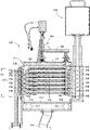
[0054] 도 5는, 본 개시내용의 실시예에 따라 구성되는 배치 경화 챔버(500)의 측단면도이다. 배치 경화 챔버(500)는, 도 1의 배치 경화 챔버(103)로서 이용될 수 있고, 위의 단계(306)에서 설명된 배치 경화 프로세스를 수행하는데 사용될 수 있다. 배치 경화 챔버(500)는 일반적으로, 챔버 바디(510), 챔버 바디(510) 내부에 배치된 다수의 경화 스테이션들(530), 및 챔버 바디(510) 내부에 부분적으로 배치된 다중 기판 리프트 어셈블리(540)를 포함한다.5 is a cross-sectional side view of a
[0055] 챔버 바디(510)는, 챔버 리드(511) 및 챔버 플로어(floor)(513)에 커플링되는 챔버 벽들(512)을 포함한다. 챔버 바디(510)로부터 프로세스 및 퍼지 가스들을 펌핑하도록 구성되는 진공 펌프 포어라인(foreline)(514)은, 챔버 플로어(513)를 통해 챔버(510)를 관통한다. 다른 실시예들에서, 진공 펌프 포어라인(514)은, 챔버 리드(511) 및/또는 챔버 벽들(512) 중 하나 또는 그 초과를 통해 챔버(510)를 관통할 수 있다. 진공 펌프 포어라인(514)은, 개구부들(521)을 통해 챔버(510)의 프로세싱 구역(522)에 그리고 다수의 경화 스테이션들(530) 각각에 인접하게 배치된 다수의 배기 유입구 어레이들(523) 각각에 유동가능하게(fluidly) 커플링된다. 따라서, 경화 프로세스 동안 기판들로부터 배출되는 프로세스 가스들, 퍼지 가스들, 및 휘발성 화합물들이 프로세싱 구역(522)에서 그리고 다수의 경화 스테이션들(530) 사이에 로케이팅되는 각각의 프로세싱 서브구역(524)에서 제거될 수 있다. 다수의 배기 유입구 어레이들(523)은 도 8과 함께 아래에서 더 상세히 설명된다.The
[0056] 챔버 바디(510)는, 챔버 벽들(512) 중 하나에 커플링되는 RPS 매니폴드(manifold)(515)를 또한 포함할 수 있다. RPS 매니폴드(515)는, 주기적인 세정 프로세스 동안, 다수의 세정 가스 개구부들(516)을 통해 세정 가스들을 각각의 프로세싱 서브구역(524)으로 지향시키도록 구성된다. 세정 가스들은 원격 플라즈마 소스(550)에 의해 생성될 수 있다. 예를 들어, NH3 또는 임의의 다른 세정 가스는 원격 플라즈마 소스를 통과할 수 있고, 그 후, 챔버 바디 및 다수의 경화 스테이션들(530)의 하나 또는 그 초과의 내부 표면들 상에서의 원하지 않는 증착 축적(deposition build-up)을 제거하기 위해 사용될 수 있다. 이러한 프로세스는, 미리결정된 양의 경화된 막이 배치 경화 챔버(500)에 의해 프로세싱된 이후 또는 미리결정된 수의 기판들이 배치 경화 챔버(500)에 의해 프로세싱된 이후 특정 시간 간격들로 수행될 수 있다.The
[0057] 챔버 바디(510)는 또한 일반적으로, 챔버 벽들(512) 중 하나에 형성되는 로딩 개구부(517), 다수의 기판 슬릿들(519)로 구성되는 슬롯형 개구부 커버(518)(도 6에 더 상세히 도시됨), 및 경화 프로세스 동안 로딩 개구부(517)를 밀봉하도록 구성되는 로딩 개구부 도어(520)를 포함한다. 로딩 개구부 도어(520)는, 슬롯형 개구부 커버(518)의 다수의 기판 슬릿들(다수의 슬롯형 개구부들)(519)을 에워싸는 밀봉 표면(526)으로 로딩 개구부(517)를 밀봉하도록 구성된다. 통상적으로, 기판 슬릿들(519) 각각은, 경화 스테이션들(530) 중 개별적인 하나에 대응하고, 실질적으로, 로딩 개구부 도어(520)가 개방 포지션에 있는 경우 대기 로봇(104)이 다수의 서브-프로세싱 구역들(524) 각각으로 암을 연장시키는 것을 허용하도록 경화 스테이션들과 정렬된다. 로딩 개구부 도어(520)는 도 5에서 폐쇄된 포지션으로 도시된다.The
[0058] 로딩 개구부(517)는, 로딩 개구부를 다수의 경화 스테이션들(530) 또는 팩토리 인터페이스(105)에 관하여 재포지셔닝(repositioning)하지 않고 기판이 다수의 경화 스테이션들(530) 각각에 로딩되게 하도록 구성된다. 예를 들어, 다수의 경화 스테이션들(530)이 도 5에 예시된 바와 같이 스택형 어레이로 배열되는 경우, 로딩 개구부(517)는, 2 차원(즉, 높이 및 폭)으로 스택형 어레이에 걸치도록 구성되어, 스택형 어레이 내의 다수의 경화 스테이션들(530) 중 대부분 또는 전부가 대기 로봇(104)에 의해 액세스가능하다. 그 결과, 경화 스테이션들(530)이 수직적인 스택형 어레이로 배열되는 경우, 다수의 경화 스테이션들(530)의 결합된 높이를 수용하기 위해 로딩 개구부(517)의 높이(525)는 비교적 크다. 슬롯형 개구부 커버(518)는, (예컨대, 기판들의 로딩 및 언로딩(unloading) 동안) 로딩 개구부(517)가 개방된 경우에 로딩 개구부(517)의 개방 면적을 최소화하거나 또는 감소시키도록 구성되는 플레이트(plate) 또는 다른 구조일 수 있다. 로딩 개구부(517)가 비교적 큰 높이(525)를 갖기 때문에, 로딩 개구부의 자유 면적이 상응하게 크며, 이는, 슬롯형 개구부 커버(518)의 부재 시에 팩토리 인터페이스(105)로부터 배치 경화 챔버(500)로의 상당한 양의 주변 공기를 허용할 수 있다. 배치 경화 챔버(500)로 진입되는 상당한 양의 주변 공기는, 배치 경화 챔버(500)의 원하지 않는 냉각, 또는 배치 경화 챔버(500)의 내부 컴포넌트들의 산화 및/또는 오염을 야기할 수 있고, 또한, 배치 경화 챔버(500) 내의 프로세스 가스들 및 배출된 생성물들이 팩토리 인터페이스(105)로 누출되는 것을 야기할 수 있다. 따라서, 슬롯형 개구부 커버(518)는, 입자들 및/또는 원하지 않는 가스들 또는 프로세싱 부산물들이 배치 경화 챔버(500)로 전달되거나 또는 그로부터 전달되는 것을 방지하도록 돕는다.The
[0059] 도 6은 본 개시내용의 실시예에 따라 구성되는, 도 5에 예시된 배치 경화 챔버(500)에 대한 슬롯형 개구부 커버(518)의 등각도이다. 슬롯형 개구부 커버(518)는, (예컨대, 기판들의 로딩 및 언로딩 동안) 로딩 개구부(517)(도 5에 도시됨)가 개방된 경우에 로딩 개구부(517)의 개방 면적을 최소화하거나 또는 감소시키도록 구성되는 플레이트 또는 다른 구조일 수 있다. 예를 들어, 다수의 기판 슬릿들(519)의 치수들은, 기판들이 로딩 개구부(517)를 통해 로딩 및 언로딩되는 것에 대해 간섭을 일으키는 것을 가능하게 하지 않으면서 실현가능한 한 작게 되도록 선택될 수 있다. 그러한 실시예들에서, 다수의 기판 슬릿들(519)의 치수들은, 대기 로봇들(104)(도 1에 도시됨), 슬롯형 개구부 커버(518), 로딩 개구부(517), 및 대기 로봇들(104)에 관한 다수의 기판 슬릿들(519)의 개별적인 포지션들에 대해 영향을 미칠 수 있는 배치 경화 챔버(500)의 임의의 컴포넌트들의 포지션의 챔버 간(chamber-to-chamber) 편차 및 누적 공차(tolerance stack-up)에 기초하여 결정될 수 있다. 따라서, 이러한 실시예들에서, 다수의 기판 슬릿들은, 대기 로봇(104)의 암 상에 놓이는 기판의 단면과 부합하는 것에 더하여, 배치 경화 챔버(500), 팩토리 인터페이스(105), 대기 로봇(104) 등의 컴포넌트들의 누적 공차를 수용하기 위한 부가적인 자유 면적에 부합하도록 구성될 수 있다.[0059] FIG. 6 is an isometric view of a slotted
[0060] 기판들이 배치 경화 챔버(500) 내로 로딩되는 동안 로딩 개구부(517)의 자유 면적을 최소화함으로써, 슬롯형 개구부 커버(518)는, 배치 경화 챔버(500) 내로의 주변 공기의 진입 및 그 외부로의 프로세스 및 퍼지 가스들의 누출을 크게 감소시키거나 또는 최소화한다. 따라서, 로딩 개구부(517)의 비교적 큰 사이즈에도 불구하고, 기판 로딩 및 언로딩 동안 프로세스 가스들 및/또는 휘발성 화합물들이 배치 경화 챔버(500)에서 거의 누출되지 않거나 또는 전혀 누출되지 않는다. 더욱이, 팩토리 인터페이스(105)로부터의 주변 공기의 진입 또는 배치 경화 챔버(500)로부터 나오는 열 방사선에 의해 야기되는 배치 경화 챔버(500)의 원하지 않는 냉각이 회피된다.[0060] By minimizing the free area of the
[0061] 도 7은, 본 개시내용의 실시예에 따라 구성되는 다수의 경화 스테이션들(530)의 부분들의 부분 단면도이다. 챔버 바디(510) 내부에 배치된 다수의 경화 스테이션들(530) 각각은, 가열된 기판 페디스털(531), 가열된 페디스털(531) 위에 포지셔닝되는 샤워헤드(532), 가열된 페디스털(531)과 샤워헤드(532) 사이에 형성되는 샤워헤드 플레넘(plenum)(533), 샤워헤드 플레넘(533) 및 프로세스 가스 패널(도시되지 않음)에 유동가능하게 커플링되는 환형 플레넘(534), 경화 스테이션 가열기(535), 및 열전대(thermocouple)(537)를 포함한다. 명확화를 위해, 경화 스테이션(530)에 인접하게 배치될 수 있는 배기 유입구 어레이(523)는 도 7에서 생략된다. 다수의 경화 스테이션들(530) 각각의 사이에 프로세싱 서브구역(524)이 로케이팅된다.7 is a partial cross-sectional view of portions of multiple curing
[0062] 가열된 기판 페디스털(531)은, 기판을 지지하고 그리고 몇몇 실시예들에서는 경화 프로세스 동안 기판을 가열하도록 구성된다. 샤워헤드(532)는, 샤워헤드 플레넘(533)으로 진입하는 프로세스 가스들(즉, 경화 가스들) 및 퍼지 가스들의 유동을 인접한 프로세싱 서브구역(524)으로 균일하게 분배하도록 구성된다. 부가하여, 가열된 기판 페디스털(531) 및 샤워헤드(532)는, 도시된 바와 같이 샤워헤드 플레넘(533)을 형성하도록 구성된다. 샤워헤드 플레넘(533)을 통과하고 그리고 프로세싱 서브구역(524)에 진입하는 가스들은, 가스들이 유동되는 프로세싱 서브구역(524)과 상이하면서 그에 인접한 프로세싱 서브구역(524)과 연관된 가열된 기판 페디스털(531)에 의해 가열될 수 있다는 것을 유의한다. 대안적으로 또는 부가적으로, 샤워헤드 플레넘(533)을 통과하고 그리고 프로세싱 서브구역(524)에 진입하는 가스들은, 샤워헤드(532)(이를 통해 가스들이 통과함)에 의해 가열될 수 있다.The
[0063] 몇몇 실시예들에서, 샤워헤드 플레넘(533)을 통과하고 그리고 프로세싱 서브구역(524)에 진입하는 프로세스 및/또는 퍼지 가스들은, 도 7에 도시된 바와 같이, 샤워헤드 플레넘(533)에 유동가능하게 커플링되는 환형 플레넘(534)을 먼저 통과할 수 있다. 환형 플레넘(534)은, 프로세스 가스들(702)이 샤워헤드 플레넘(533)을 통해 유동하는 경우에 프로세스 가스들(702) 상에 생성된 유동 저항보다 더 큰 유동 저항(즉, 압력 강하)을 프로세스 가스들(702) 상에 생성하도록 사이징된 복수의 오리피스(orifice)들(701)로 구성될 수 있다. 이러한 방식에서, 환형 플레넘(534)이 단일 유입구 또는 적은 수의 유입구들을 통해 프로세스 가스 패널에 커플링될 수 있다 하더라도, 샤워헤드 플레넘(533)으로의 프로세스 가스들(702)의 유동은 샤워헤드(532)의 원주 둘레에서 실질적으로 균일할 것이다. 일반적으로, 샤워헤드 플레넘(533)으로의 프로세스 가스들(702)의 균일한 유동은, 샤워헤드(532)를 통한 프로세싱 서브구역(524)으로의 균일한 유동을 가능하게 한다. 프로세스 가스들(702)의 균일한 유동을 추가적으로 가능하게 하기 위해, 환형 플레넘(534)의 내부 둘레 주변에 오리피스(701)들이 대칭적으로 분포될 수 있다.[0063] In some embodiments, process and/or purge gases passing through
[0064] 샤워헤드 플레넘(533)으로의 프로세스 가스들(702)의 균일한 유동을 계속 가능하게 하는, 오리피스들(701)의 최대 자유 면적은, 다른 것들 중에서도, 오리피스들(701)의 수, 샤워헤드 플레넘(533)의 치수들, 샤워헤드(532)에 의해 생성되는 유동 저항, 및 프로세스 가스들(702)의 적절한 유량에 기초하여 결정될 수 있다. 오리피스들(701)의 그러한 최대 자유 면적은, 위에-설명된 팩터들에 대한 정보가 주어진 당업자에 의해 결정될 수 있다.The maximum free area of the
[0065] 배치 경화 챔버(500)는 경화 스테이션 가열기(535) 및 열전대(537)를 포함할 수 있으며, 이들은 함께, 다수의 경화 스테이션들(530) 각각에 대한 개별적인 폐쇄-루프 온도 제어를 가능하게 한다. 따라서, 배치 경화 챔버(500)는, 다수의 경화 스테이션들(530) 간의 온도 편차에 의해 야기되는 기판 간 편차들의 위험성 없이 다수의 기판들을 프로세싱할 수 있다. 배치 경화 챔버(500)의 상단 및 하단 프로세싱 서브구역들(524)에서 프로세싱되는 기판들은 통상적으로, 경화 스테이션 가열기(535)의 개별적인 온도 제어 없이, 중앙의 프로세싱 서브구역들(524)에서 프로세싱되는 기판들보다 더 낮은 온도들에 노출되며, 이는, 경화 프로세스의 웨이퍼 간(wafer-to-wafer) 배치 프로세싱 결과들에 상당한 영향을 미칠 수 있다.The
[0066] 몇몇 실시예들에서, 열전대(537) 및 경화 스테이션 가열기(535) 둘 모두는, 도 7에 도시된 바와 같이, 가열된 기판 페디스털(531) 내에 배치된다. 그러한 실시예들에서, 샤워헤드(532) 및 환형 플레넘(534)의 벽들은, 전도성 및 방사성 열 전달을 통해, 가열된 기판 페디스털(531)의 온도에 가까운 온도로 가열된다. 그 결과, 환형 플레넘(534), 샤워헤드 플레넘(533), 및 샤워헤드(532)를 통과하는 프로세스 가스들이 또한, 가열된 기판 페디스털(531)의 온도에 근사적인 온도로 가열된다. 열전대(537)는, 가열된 기판 페디스털(531)의 온도, 및 그에 따라 프로세싱 서브구역들(524) 중 하나에 진입하는 프로세스 가스들의 온도의 폐쇄-루프 제어를 위한 온도 피드백을 제공한다. 대안적으로, 열전대(537)는, 샤워헤드(532)와 접촉하여 그리고/또는 프로세싱 서브구역들(524) 중 하나에 진입하고 있는 프로세스 가스들과 접촉하여 배치될 수 있다.In some embodiments, both the
[0067] 위에 언급된 바와 같이, 다수의 경화 스테이션들(530) 각각에 인접하게 다수의 배기 유입구 어레이들(523)이 배치된다. 프로세싱 서브구역들(524) 중 하나에서 기판 상에 수행되는 몇몇 경화 프로세스들에서, 기판 상에 형성된 유전체 막으로부터 배출되는 휘발성 컴포넌트들은, SiO2 미립자들과 같은 미립자들을 형성할 수 있다. 이들 미립자들은 프로세싱되고 있는 기판 상에 남아 있게 될 수 있으며, 이는 매우 바람직하지 않다. 그 결과, 배치 경화 챔버(500) 내의 퍼지 가스 및 프로세스 가스의 유동 패턴은, 프로세싱 서브구역(524)에 있는 기판 상의 입자 오염에 영향을 미칠 수 있다. 배기 유입구 어레이들(523)은, 배출된 휘발성 컴포넌트들 및 미립자들이 형성되면, 프로세싱되고 있는 기판으로부터 떨어지게 그들을 드로잉(draw)하도록 구성된다. 몇몇 실시예들에서, 도 7 및 도 8a-8c에 예시된 바와 같이, 각각의 경화 스테이션(530)에 인접하게, 예를 들어, 대칭적 어레인지먼트(arrangement)로 2개 또는 그 초과의 배기 유입구 어레이들(523)이 배치된다.As noted above, a plurality of
[0068] 도 8a는, 본 개시내용의 실시예에 따라 배열되는 배기 유입구 어레이들(523)의 다수의 그룹들의 등각도이다. 도 8b는, 도 8a에 도시된 배기 유입구 어레이들(523)의 다수의 그룹들의 평면도이고, 도 8c는, 도 8a에 도시된 배기 유입구 어레이들(523)의 다수의 그룹들의 측면도이다. 명확화를 위해, 배치 경화 챔버(500)의 대부분의 다른 엘리먼트들은 생략된다. 도시된 바와 같이, 도 8a-8c에 예시된 실시예에서, 4개의 배기 유입구 어레이들(523)의 그룹은, 4개의 배기 유입구 어레이들(523)의 총 6개의 그룹들에 대해 특정 경화 스테이션(530)에 인접하도록 포지셔닝된다. 다른 실시예들에서, 배기 유입구 어레이들(523) 중 4개보다 더 많거나 또는 더 적은 배기 유입구 어레이들의 그룹이 단일 경화 스테이션(530)에 인접하게 포지셔닝될 수 있다.8A is an isometric view of multiple groups of
[0069] 각각의 배기 유입구 어레이(523)는, 배기 유입구 어레이(523) 내부에 로케이팅되는 배기 플레넘(802)에 유동가능하게 커플링되는 복수의 배기 유입구들(801)을 포함한다. 몇몇 실시예들에서, 각각의 배기 유입구 어레이(523)는, 지지 부재(810)(이에 커플링된 배기 유입구 어레이(523)를 구조적으로 지지하고 포지셔닝함)에 기계적으로 커플링된다. 도 8a-c에 예시된 실시예에서는 배치 경화 챔버(500)가 4개의 별개의 지지 부재들(810)을 포함하는 반면, 다른 실시예들에서, 배치 경화 챔버(500)는 4개보다 더 많거나 또는 더 적은 총 지지 부재들(810)로 구성될 수 있다. 부가하여, 각각의 배기 유입구 어레이(523)는 배기 매니폴드(명확화를 위해 도시되지 않음)에 유동가능하게 커플링되며, 배기 매니폴드는 결국, 배치 경화 챔버(500)(도 5에 도시됨)의 포어라인(514)에 유동가능하게 커플링된다. 몇몇 실시예들에서, 지지 부재들(810) 중 하나 또는 그 초과가 또한 배기 매니폴드로서 구성될 수 있다.Each
[0070] 몇몇 실시예들에서, 배기 유입구 어레이들(523) 중 일부 또는 그 전부는, 유동-밸런싱(flow-balancing) 오리피스(811)를 포함할 수 있다. 그러한 실시예들에서, 각각의 유동-밸런싱 오리피스(811)는, 각각의 배기 유입구 어레이(523)를 통한 프로세스 가스들 및 배출 컴포넌트들의 유동이 인접한 배기 유입구 어레이들(523)에 대해 동등하게 되거나 또는 실질적으로 동등하게 되도록, 연관된 배기 유입구 어레이(523)로의 유동을 제한하도록 구성된다. 몇몇 실시예들에서, 유동-밸런싱 오리피스들(811)은 고정형 오리피스들이다. 그러한 실시예들에서, 각각의 고정형 오리피스의 특정 사이즈는, 컴퓨터 시뮬레이션들, 유동 시각화, 시행 착오 방법들, 또는 이들의 임의의 결합을 사용하여 결정될 수 있다. 다른 실시예들에서, 유동-밸런싱 오리피스들(811) 중 일부 또는 그 전부는 조정가능한 오리피스들(이를테면, 니들 밸브(needle valve)들)이며, 이들은, 제조 시에, 현장에서, 그리고/또는 배치 경화 챔버(500)의 배기 밸런스 이슈들에 대한 응답으로 셋팅될 수 있다.In some embodiments, some or all of the
[0071] 다중 기판 리프트 어셈블리(540)는, 로딩 및 언로딩 동안, 대기 로봇(104)으로부터 개별적인 기판들을 제거하고 그리고 대기 로봇(104) 상에 개별적인 기판들을 배치하도록 구성된다. 부가하여, 다중 기판 리프트 어셈블리(540)는, 배치 경화 챔버(500)에서의 프로세싱 동안 다수의 기판들을 동시에 포지셔닝시키도록 구성된다. 예를 들어, 몇몇 실시예들에서, 다중 기판 리프트 어셈블리(540)는, 프로세싱되는 각각의 기판을 프로세싱 포지션으로 그리고 예열 포지션으로 동시에 포지셔닝시키도록 구성된다. 일반적으로, 기판은, 프로세싱 포지션에 있는 경우에는 샤워헤드(532)에 근접하게 포지셔닝되고, 예열 포지션에 있는 경우에는 가열된 기판 페디스털(531) 상에 포지셔닝된다.The
[0072] 다중 기판 리프트 어셈블리(540)는, 다수(예컨대, 3개 또는 그 초과)의 리프트 핀 인덱서들(541)을 포함한다. 도 5에 예시된 실시예에서, 다중 기판 리프트 어셈블리(540)는 3개의 리프트 핀 인덱서들(541)을 포함하지만, 하나만이 가시적이다. 도 9는 다중 기판 리프트 어셈블리(540)의 3개의 리프트 핀 인덱서들(541) 전부의 부분들 및 챔버 리드(511)의 등각도이다. 명확화를 위해, 챔버 벽들(512) 및 챔버 플로어(513)는 도 9에서 생략된다. 3개의 리프트 핀 인덱서들(541) 각각은, 챔버 바디(510) 내부에 부분적으로 배치되고 리프트 메커니즘(544)(도 5에 도시되며 명확화를 위해 도 9에서는 생략됨)에 커플링된다. 리프트 메커니즘(544)은, 위에 설명된 바와 같이, 로딩, 언로딩, 예열, 및 프로세싱 포지션들로 기판들을 포지셔닝시키기에 적절한 임의의 기계적 액츄에이터(actuator)일 수 있다. 예를 들어, 리프트 메커니즘은, 압축공기식(pneumatic) 액츄에이터, 스텝퍼(stepper) 모터 등을 포함할 수 있다.The multiple
[0073] 도 10은, 본 개시내용의 실시예에 따라 구성되는 리프트 핀 인덱서(541)의 단면도이다. 도시된 바와 같이, 리프트 핀 인덱서(541)는 일반적으로, 배치 경화 챔버(500)의 프로세싱 서브구역들(524) 각각에 대해 하나의 리프트 핀(542)을 포함한다. 따라서, 도 5, 도 9, 및 도 10에 예시된 예에서, 각각의 리프트 핀 인덱서(541)는, 수직 샤프트(shaft)(543)에 커플링되는 6개의 리프트 핀들(542)을 포함한다. 3개의 리프트 핀 인덱서들(541)은, 6개의 기판들을 프로세싱 포지션에 동시에 포지셔닝시킬 수 있거나 또는 6개의 기판들을 예열 포지션에 있는 개별적인 가열된 기판 페디스털(531) 상에 동시에 셋팅할 수 있다.10 is a cross-sectional view of a
[0074] 몇몇 실시예들에서, 각각의 리프트 핀(542)은, 프로세싱 동안 기판으로부터 리프트 핀들(542)로의 열 전달을 감소시키고 그리고/또는 최소화하기 위해, 저-접촉(low-contact) 열적 격리 접촉 표면(1001)으로 구성된다. 이러한 방식으로, 프로세싱 동안 기판 상의 소위 "콜드 스폿(cold spot)들"이 감소되거나 또는 제거되며, 그에 의해, 배치 경화 챔버(500)에서 경화되는 유전체 막의 균일성이 개선된다. 몇몇 실시예들에서, 접촉 표면(1001)은, 기판과 접촉 표면(1001) 사이의 접촉 영역이 선 접촉 또는 점 접촉으로 감소되도록, 원통형 엘리먼트(1002)로 형성된다. 부가하여, 원통형 엘리먼트(1002)는, 리프트 핀들(542)을 형성하는데 통상적으로 사용되는 재료들보다 더 낮은 열 전도 계수를 갖는 재료, 이를테면 알루미늄 및 스테인리스 강으로 형성될 수 있다. 예를 들어, 몇몇 실시예들에서, 원통형 엘리먼트(1002)는 사파이어(Al2O3)로 형성될 수 있다.In some embodiments, each
[0075] 요약하면, 본 개시내용의 하나 또는 그 초과의 실시예들은, 일반적으로 배치 프로세싱과 연관된 기판 간 편차 없이 다수의 기판들 상에 배치된 유전체 재료를 경화시키기 위한 시스템들 및 방법들을 제공한다. 구체적으로는, 배치 경화 챔버는, 각각이 독립적으로 온도 제어되는 다수의 프로세싱 서브-구역들을 포함한다. 부가하여, 챔버의 로딩 개구부 상에 탑재된 슬롯형 커버는, 로딩 및 언로딩 동안 챔버에 진입하는 주변 공기의 효과를 크게 감소시킨다.[0075] In summary, one or more embodiments of the present disclosure provide systems and methods for curing dielectric material disposed on multiple substrates without the substrate-to-substrate variation generally associated with batch processing. . Specifically, the batch curing chamber includes a plurality of processing sub-zones, each independently temperature controlled. In addition, the slotted cover mounted on the loading opening of the chamber greatly reduces the effect of ambient air entering the chamber during loading and unloading.
[00010] 전술한 내용은 본 개시내용의 실시예들에 관한 것이지만, 본 개시내용의 다른 그리고 추가적인 실시예들이 본 개시내용의 기본적인 범위로부터 벗어나지 않으면서 안출될 수 있으며, 본 개시내용의 범위는 하기의 청구항들에 의해 결정된다.[00010] While the foregoing relates to embodiments of the present disclosure, other and additional embodiments of the disclosure may be devised without departing from the basic scope of the disclosure, the scope of the disclosure being determined by the claims of
Claims (15)
메인프레임;
적어도 하나의 대기 로봇(atmospheric robot)을 포함하고 그리고 기판들의 하나 또는 그 초과의 카세트(cassette)들을 수용하도록 구성되는 팩토리 인터페이스(factory interface);
상기 메인프레임에 커플링되고 그리고 상기 팩토리 인터페이스의 상기 적어도 하나의 대기 로봇으로부터 하나 또는 그 초과의 기판들을 수용하도록 구성되는 로드 록 챔버(load lock chamber);
상기 메인프레임에 각각 커플링되는 다수의 유동성 CVD 챔버들; 및
상기 팩토리 인터페이스에 커플링되는 배치(batch) 프로세싱 챔버를 포함하며,
상기 배치 프로세싱 챔버는,
다수의 서브-프로세싱 구역들 ― 상기 다수의 서브-프로세싱 구역들 각각은, 상기 적어도 하나의 대기 로봇으로부터 기판을 수용하고 그리고 상기 대기 로봇으로부터 수용된 기판 상에서 경화(curing) 프로세스를 수행하도록 구성됨 ―;
상기 배치 프로세싱 챔버의 벽에 형성되는 로딩 개구부(loading opening);
상기 로딩 개구부 위에 배치되는 제 1 도어; 및
다수의 슬롯형(slotted) 개구부들을 포함하고 그리고 상기 로딩 개구부 위에 배치되는 커버 플레이트(cover plate)
를 포함하고,
상기 제 1 도어는 상기 다수의 슬롯형 개구부들의 전부 위에 배치되고,
상기 제 1 도어는, 상기 다수의 슬롯형 개구부들을 에워싸는 밀봉 표면으로 상기 로딩 개구부를 밀봉하도록 구성되고,
상기 다수의 슬롯형 개구부들 각각은, 상기 적어도 하나의 대기 로봇이 상기 배치 프로세싱 챔버 외부의 포지션으로부터 상기 다수의 서브-프로세싱 구역들 중 하나로 암(arm)을 연장시키게 하도록 구성되고,
상기 다수의 슬롯형 개구부들 각각은, 상기 로딩 개구부가 개방된 경우 상기 로딩 개구부의 자유 면적(free area)을 감소시키도록 구성되는,
기판의 표면 상에 유전체 재료를 형성하기 위한 시스템.A system for forming a dielectric material on a surface of a substrate, comprising:
mainframe;
a factory interface comprising at least one atmospheric robot and configured to receive one or more cassettes of substrates;
a load lock chamber coupled to the mainframe and configured to receive one or more substrates from the at least one standby robot of the factory interface;
a plurality of flowable CVD chambers each coupled to the mainframe; and
a batch processing chamber coupled to the factory interface;
The batch processing chamber,
a plurality of sub-processing zones, each of the plurality of sub-processing zones configured to receive a substrate from the at least one atmospheric robot and perform a curing process on the substrate received from the atmospheric robot;
a loading opening formed in a wall of the batch processing chamber;
a first door disposed over the loading opening; and
a cover plate including a plurality of slotted openings and disposed over the loading opening;
including,
the first door is disposed over all of the plurality of slotted openings;
the first door is configured to seal the loading opening with a sealing surface surrounding the plurality of slotted openings;
each of the plurality of slotted openings is configured to cause the at least one standby robot to extend an arm from a position outside the batch processing chamber into one of the plurality of sub-processing regions;
each of the plurality of slotted openings is configured to reduce a free area of the loading opening when the loading opening is open;
A system for forming a dielectric material on a surface of a substrate.
상기 다수의 슬롯형 개구부들 각각은, 상기 다수의 서브-프로세싱 구역들 중 하나의 서브-프로세싱 구역에 대응하고,
상기 다수의 슬롯형 개구부들 각각은, 상기 도어의 형상 및 상기 로딩 개구부의 형상에 대해 비대칭인 형상을 갖는,
기판의 표면 상에 유전체 재료를 형성하기 위한 시스템.The method of claim 1,
each of the plurality of slotted openings corresponds to one sub-processing zone of the plurality of sub-processing zones;
each of the plurality of slotted openings has a shape that is asymmetric with respect to a shape of the door and a shape of the loading opening;
A system for forming a dielectric material on a surface of a substrate.
상기 다수의 슬롯형 개구부들 각각은, 상기 다수의 서브-프로세싱 구역들 중 대응하는 서브-프로세싱 구역과 정렬되고,
상기 다수의 슬롯형 개구부들 각각은, 상기 도어의 형상 및 상기 로딩 개구부의 형상에 비해 더 많은 엣지를 갖는 형상을 포함하는,
기판의 표면 상에 유전체 재료를 형성하기 위한 시스템.3. The method of claim 2,
each of the plurality of slotted openings is aligned with a corresponding one of the plurality of sub-processing zones;
each of the plurality of slotted openings comprises a shape having more edges compared to a shape of the door and a shape of the loading opening;
A system for forming a dielectric material on a surface of a substrate.
상기 로딩 개구부는, 상기 로딩 개구부를 다수의 경화 스테이션들 또는 상기 팩토리 인터페이스에 관하여 재포지셔닝(repositioning)시킴이 없이 기판이 상기 다수의 경화 스테이션들 각각에 로딩되게 하도록 구성되는,
기판의 표면 상에 유전체 재료를 형성하기 위한 시스템.The method of claim 1,
wherein the loading opening is configured to allow a substrate to be loaded into each of the plurality of curing stations without repositioning the loading opening with respect to the plurality of curing stations or the factory interface.
A system for forming a dielectric material on a surface of a substrate.
상기 다수의 유동성 CVD 챔버들 각각은, CVD 프로세스를 통해 기판 상에 유동성 유전체 층을 증착하도록 구성되는,
기판의 표면 상에 유전체 재료를 형성하기 위한 시스템.The method of claim 1,
each of the plurality of flowable CVD chambers is configured to deposit a flowable dielectric layer on a substrate via a CVD process;
A system for forming a dielectric material on a surface of a substrate.
상기 다수의 서브-프로세싱 구역들은 스택형(stacked) 어레이로 배열되고, 상기 로딩 개구부는 2차원으로 상기 스택형 어레이에 걸치도록 구성되는,
기판의 표면 상에 유전체 재료를 형성하기 위한 시스템.The method of claim 1,
wherein the plurality of sub-processing regions are arranged in a stacked array, and wherein the loading opening is configured to span the stacked array in two dimensions;
A system for forming a dielectric material on a surface of a substrate.
상기 팩토리 인터페이스는, 상기 배치 프로세싱 챔버에서 프로세싱되기에 앞서 상기 배치 프로세싱 챔버 외부에 기판들을 일시적으로 저장하도록 구성되는 적어도 하나의 대기 홀딩(atmospheric holding) 스테이션을 더 포함하는,
기판의 표면 상에 유전체 재료를 형성하기 위한 시스템.The method of claim 1,
wherein the factory interface further comprises at least one atmospheric holding station configured to temporarily store substrates outside the batch processing chamber prior to being processed in the batch processing chamber.
A system for forming a dielectric material on a surface of a substrate.
상기 배치 프로세싱 챔버의 상기 다수의 서브-프로세싱 구역들 각각은, 가열된 기판 페디스털(pedestal)과 샤워헤드(showerhead) 사이에 배치되는,
기판의 표면 상에 유전체 재료를 형성하기 위한 시스템.The method of claim 1,
each of the plurality of sub-processing regions of the batch processing chamber is disposed between a heated substrate pedestal and a showerhead;
A system for forming a dielectric material on a surface of a substrate.
상기 샤워헤드는, 서브-프로세싱 구역에 배치된 기판에 프로세스 가스를 독립적으로 전달하도록 구성되는,
기판의 표면 상에 유전체 재료를 형성하기 위한 시스템.9. The method of claim 8,
wherein the showerhead is configured to independently deliver a process gas to a substrate disposed in a sub-processing region;
A system for forming a dielectric material on a surface of a substrate.
상기 가열된 기판 페디스털은, 프로세싱 동안, 서브-프로세싱 구역에 배치된 기판을 독립적으로 가열하도록 구성되는,
기판의 표면 상에 유전체 재료를 형성하기 위한 시스템.9. The method of claim 8,
wherein the heated substrate pedestal is configured to independently heat a substrate disposed in a sub-processing region during processing;
A system for forming a dielectric material on a surface of a substrate.
다수의 서브-프로세싱 구역들 ― 상기 다수의 서브-프로세싱 구역들 각각은, 대기 로봇으로부터 기판을 수용하고 그리고 상기 대기 로봇으로부터 수용된 기판 상에서 경화 프로세스를 수행하도록 구성됨 ―;
상기 배치 프로세싱 챔버의 벽에 형성되는 로딩 개구부;
상기 로딩 개구부 위에 배치되는 제 1 도어; 및
다수의 슬롯형 개구부들을 포함하는, 상기 로딩 개구부 위에 배치되는 커버 플레이트를 포함하며,
상기 제 1 도어는 상기 다수의 슬롯형 개구부들의 전부 위에 배치되고,
상기 제 1 도어는, 상기 다수의 슬롯형 개구부들을 에워싸는 밀봉 표면으로 상기 로딩 개구부를 밀봉하도록 구성되고,
상기 슬롯형 개구부들 각각은, 적어도 하나의 대기 로봇이 상기 배치 프로세싱 챔버 외부의 포지션으로부터 상기 다수의 서브-프로세싱 구역들 중 하나로 암을 연장시키게 하도록 구성되고,
상기 다수의 슬롯형 개구부들 각각은, 상기 로딩 개구부가 개방된 경우 상기 로딩 개구부의 자유 면적을 감소시키도록 구성되는,
배치 프로세싱 챔버.A batch processing chamber comprising:
a plurality of sub-processing zones, each of the plurality of sub-processing zones configured to receive a substrate from an atmospheric robot and perform a curing process on the substrate received from the atmospheric robot;
a loading opening formed in a wall of the batch processing chamber;
a first door disposed over the loading opening; and
a cover plate disposed over the loading opening, the cover plate including a plurality of slotted openings;
the first door is disposed over all of the plurality of slotted openings;
the first door is configured to seal the loading opening with a sealing surface surrounding the plurality of slotted openings;
each of the slotted openings is configured to cause at least one atmospheric robot to extend an arm from a position outside the batch processing chamber to one of the plurality of sub-processing regions;
each of the plurality of slotted openings is configured to reduce a free area of the loading opening when the loading opening is open;
Batch processing chamber.
상기 다수의 슬롯형 개구부들 각각은, 상기 다수의 서브-프로세싱 구역들 중 하나의 서브-프로세싱 구역에 대응하고,
상기 다수의 슬롯형 개구부들 각각은, 상기 도어의 형상 및 상기 로딩 개구부의 형상에 대해 비대칭인 형상을 갖는,
배치 프로세싱 챔버.12. The method of claim 11,
each of the plurality of slotted openings corresponds to one sub-processing zone of the plurality of sub-processing zones;
each of the plurality of slotted openings has a shape that is asymmetric with respect to a shape of the door and a shape of the loading opening;
Batch processing chamber.
상기 다수의 슬롯형 개구부들 각각은, 상기 다수의 서브-프로세싱 구역들 중 대응하는 서브-프로세싱 구역과 정렬되고,
상기 다수의 슬롯형 개구부들 각각은, 상기 도어의 형상 및 상기 로딩 개구부의 형상에 비해 더 많은 엣지를 갖는 형상을 포함하는,
배치 프로세싱 챔버.13. The method of claim 12,
each of the plurality of slotted openings is aligned with a corresponding one of the plurality of sub-processing zones;
each of the plurality of slotted openings comprises a shape having more edges compared to a shape of the door and a shape of the loading opening;
Batch processing chamber.
상기 로딩 개구부는, 상기 로딩 개구부를 다수의 경화 스테이션들에 관하여 재포지셔닝시킴이 없이 기판이 상기 다수의 경화 스테이션들 각각에 로딩되게 하도록 구성되는,
배치 프로세싱 챔버. 12. The method of claim 11,
wherein the loading opening is configured to allow a substrate to be loaded into each of the plurality of curing stations without repositioning the loading opening with respect to the plurality of curing stations;
Batch processing chamber.
상기 배치 프로세싱 챔버의 상기 다수의 서브-프로세싱 구역들 각각은, 가열된 기판 페디스털과 샤워헤드 사이에 배치되는,
배치 프로세싱 챔버.12. The method of claim 11,
each of the plurality of sub-processing regions of the batch processing chamber is disposed between a heated substrate pedestal and a showerhead;
Batch processing chamber.
Priority Applications (1)
| Application Number | Priority Date | Filing Date | Title |
|---|---|---|---|
| KR1020227019130A KR102500194B1 (en) | 2014-05-14 | 2015-04-21 | Batch curing chamber with gas distribution and individual pumping |
Applications Claiming Priority (5)
| Application Number | Priority Date | Filing Date | Title |
|---|---|---|---|
| US201461996817P | 2014-05-14 | 2014-05-14 | |
| US61/996,817 | 2014-05-14 | ||
| US14/577,828 | 2014-12-19 | ||
| US14/577,828 US10113236B2 (en) | 2014-05-14 | 2014-12-19 | Batch curing chamber with gas distribution and individual pumping |
| PCT/US2015/026937 WO2015175175A1 (en) | 2014-05-14 | 2015-04-21 | Batch curing chamber with gas distribution and individual pumping |
Related Child Applications (1)
| Application Number | Title | Priority Date | Filing Date |
|---|---|---|---|
| KR1020227019130A Division KR102500194B1 (en) | 2014-05-14 | 2015-04-21 | Batch curing chamber with gas distribution and individual pumping |
Publications (2)
| Publication Number | Publication Date |
|---|---|
| KR20170007411A KR20170007411A (en) | 2017-01-18 |
| KR102407734B1 true KR102407734B1 (en) | 2022-06-10 |
Family
ID=54480423
Family Applications (3)
| Application Number | Title | Priority Date | Filing Date |
|---|---|---|---|
| KR1020167034905A KR102407734B1 (en) | 2014-05-14 | 2015-04-21 | Batch curing chamber with gas distribution and individual pumping |
| KR1020227019130A KR102500194B1 (en) | 2014-05-14 | 2015-04-21 | Batch curing chamber with gas distribution and individual pumping |
| KR1020237004775A KR102588544B1 (en) | 2014-05-14 | 2015-04-21 | Batch curing chamber with gas distribution and individual pumping |
Family Applications After (2)
| Application Number | Title | Priority Date | Filing Date |
|---|---|---|---|
| KR1020227019130A KR102500194B1 (en) | 2014-05-14 | 2015-04-21 | Batch curing chamber with gas distribution and individual pumping |
| KR1020237004775A KR102588544B1 (en) | 2014-05-14 | 2015-04-21 | Batch curing chamber with gas distribution and individual pumping |
Country Status (5)
| Country | Link |
|---|---|
| US (3) | US10113236B2 (en) |
| JP (2) | JP6592012B2 (en) |
| KR (3) | KR102407734B1 (en) |
| CN (3) | CN106463362B (en) |
| WO (1) | WO2015175175A1 (en) |
Families Citing this family (15)
| Publication number | Priority date | Publication date | Assignee | Title |
|---|---|---|---|---|
| US9226407B2 (en) * | 2002-07-01 | 2015-12-29 | Semigear Inc | Reflow treating unit and substrate treating apparatus |
| US9355922B2 (en) | 2014-10-14 | 2016-05-31 | Applied Materials, Inc. | Systems and methods for internal surface conditioning in plasma processing equipment |
| US9966240B2 (en) | 2014-10-14 | 2018-05-08 | Applied Materials, Inc. | Systems and methods for internal surface conditioning assessment in plasma processing equipment |
| US11482434B2 (en) | 2016-10-18 | 2022-10-25 | Belting E-Town Semiconductor Technology Co., Ltd | Systems and methods for workpiece processing |
| US10840068B2 (en) * | 2017-02-15 | 2020-11-17 | Yield Engineering Systems, Inc. | Plasma spreading apparatus and method of spreading plasma in process ovens |
| WO2018193753A1 (en) * | 2017-04-17 | 2018-10-25 | 東京エレクトロン株式会社 | Insulating film forming method, insulating film forming device, and substrate processing system |
| CN117524976A (en) * | 2017-05-13 | 2024-02-06 | 应用材料公司 | Cyclical flowable deposition and high density plasma processing for high quality gap-fill schemes |
| KR102405723B1 (en) * | 2017-08-18 | 2022-06-07 | 어플라이드 머티어리얼스, 인코포레이티드 | High pressure and high temperature annealing chamber |
| US10872762B2 (en) * | 2017-11-08 | 2020-12-22 | Taiwan Semiconductor Manufacturing Company, Ltd. | Methods of forming silicon oxide layer and semiconductor structure |
| US11101163B2 (en) * | 2018-01-30 | 2021-08-24 | Taiwan Semiconductor Manufacturing Co., Ltd. | Systems and methods for automated robotic arm sensing |
| US10734219B2 (en) * | 2018-09-26 | 2020-08-04 | Asm Ip Holdings B.V. | Plasma film forming method |
| US20210013069A1 (en) * | 2019-07-12 | 2021-01-14 | Applied Materials, Inc. | Multi-lid structure for semiconductor processing system |
| JP7333762B2 (en) | 2020-02-05 | 2023-08-25 | 東京エレクトロン株式会社 | Plasma processing apparatus and plasma processing method |
| US11901222B2 (en) * | 2020-02-17 | 2024-02-13 | Applied Materials, Inc. | Multi-step process for flowable gap-fill film |
| JP7156332B2 (en) * | 2020-05-21 | 2022-10-19 | 株式会社安川電機 | Conveying Device, Conveying Method and Conveying System |
Citations (3)
| Publication number | Priority date | Publication date | Assignee | Title |
|---|---|---|---|---|
| US20030173347A1 (en) * | 2002-03-15 | 2003-09-18 | Guiver Harold Chris | Vacuum thermal annealer |
| US20070209593A1 (en) * | 2006-03-07 | 2007-09-13 | Ravinder Aggarwal | Semiconductor wafer cooling device |
| US20090016853A1 (en) * | 2007-07-09 | 2009-01-15 | Woo Sik Yoo | In-line wafer robotic processing system |
Family Cites Families (25)
| Publication number | Priority date | Publication date | Assignee | Title |
|---|---|---|---|---|
| US4264393A (en) * | 1977-10-31 | 1981-04-28 | Motorola, Inc. | Reactor apparatus for plasma etching or deposition |
| US6296735B1 (en) * | 1993-05-03 | 2001-10-02 | Unaxis Balzers Aktiengesellschaft | Plasma treatment apparatus and method for operation same |
| CH687987A5 (en) * | 1993-05-03 | 1997-04-15 | Balzers Hochvakuum | A process for the increase of the deposition rate in a plasma discharge space and plasma chamber. |
| JPH07297194A (en) * | 1994-04-25 | 1995-11-10 | Sony Corp | Multichamber apparatus and manufacture of semiconductor device |
| JP3421483B2 (en) * | 1995-08-25 | 2003-06-30 | 株式会社東芝 | Method for manufacturing semiconductor device |
| US5879459A (en) * | 1997-08-29 | 1999-03-09 | Genus, Inc. | Vertically-stacked process reactor and cluster tool system for atomic layer deposition |
| US6610150B1 (en) | 1999-04-02 | 2003-08-26 | Asml Us, Inc. | Semiconductor wafer processing system with vertically-stacked process chambers and single-axis dual-wafer transfer system |
| JP5021112B2 (en) * | 2000-08-11 | 2012-09-05 | キヤノンアネルバ株式会社 | Vacuum processing equipment |
| KR100491161B1 (en) * | 2002-11-26 | 2005-05-24 | 주식회사 테라세미콘 | Semiconductor manufacturing system for thermal process |
| JP4673290B2 (en) * | 2003-02-14 | 2011-04-20 | アプライド マテリアルズ インコーポレイテッド | Cleaning native oxides with hydrogen-containing radicals |
| JP4319434B2 (en) * | 2003-03-11 | 2009-08-26 | 東京エレクトロン株式会社 | Gate valve and vacuum vessel |
| CN101061253B (en) | 2004-11-22 | 2010-12-22 | 应用材料股份有限公司 | Substrate processing apparatus using a batch processing chamber |
| US20070084408A1 (en) | 2005-10-13 | 2007-04-19 | Applied Materials, Inc. | Batch processing chamber with diffuser plate and injector assembly |
| WO2008004278A1 (en) * | 2006-07-04 | 2008-01-10 | Toshiba Mitsubishi-Electric Industrial Systems Corporation | Apparatus for concentrating/diluting specific gas and method of concentrating/diluting specific gas |
| JP2010047818A (en) * | 2008-08-25 | 2010-03-04 | Toshiba Corp | Semiconductor manufacturing equipment and semiconductor manufacturing method |
| KR101458195B1 (en) | 2009-09-25 | 2014-11-05 | 주식회사 티지오테크 | Batch Type Apparatus For Forming Epitaxial Layer And Method For The Same |
| US8524004B2 (en) * | 2010-06-16 | 2013-09-03 | Applied Materials, Inc. | Loadlock batch ozone cure |
| KR101223489B1 (en) * | 2010-06-30 | 2013-01-17 | 삼성디스플레이 주식회사 | Apparatus for Processing Substrate |
| US9285168B2 (en) | 2010-10-05 | 2016-03-15 | Applied Materials, Inc. | Module for ozone cure and post-cure moisture treatment |
| KR101528138B1 (en) * | 2011-01-18 | 2015-06-12 | 가부시키가이샤 히다치 고쿠사이 덴키 | Substrate processing apparatus, substrate supporting tool and method of manufacturing semiconductor device |
| CN103493185A (en) * | 2011-04-08 | 2014-01-01 | 应用材料公司 | Apparatus and method for UV treatment, chemical treatment, and deposition |
| JPWO2013054652A1 (en) * | 2011-10-11 | 2015-03-30 | 株式会社日立国際電気 | Substrate processing apparatus, substrate processing method, semiconductor device manufacturing method, and recording medium |
| WO2013173999A1 (en) * | 2012-05-24 | 2013-11-28 | Acm Research (Shanghai) Inc. | Loadlock chamber and method for treating substrates using the same |
| JP5977274B2 (en) * | 2013-03-21 | 2016-08-24 | 東京エレクトロン株式会社 | Batch type vertical substrate processing apparatus and substrate holder |
| US20150044619A1 (en) * | 2013-08-07 | 2015-02-12 | International Business Machines Corporation | Carrier for Ultra-Thin Substrates and Method of Use |
-
2014
- 2014-12-19 US US14/577,828 patent/US10113236B2/en active Active
-
2015
- 2015-04-21 CN CN201580025098.9A patent/CN106463362B/en active Active
- 2015-04-21 KR KR1020167034905A patent/KR102407734B1/en active IP Right Grant
- 2015-04-21 WO PCT/US2015/026937 patent/WO2015175175A1/en active Application Filing
- 2015-04-21 JP JP2016567489A patent/JP6592012B2/en active Active
- 2015-04-21 CN CN201911127078.9A patent/CN110828346B/en active Active
- 2015-04-21 KR KR1020227019130A patent/KR102500194B1/en active IP Right Grant
- 2015-04-21 CN CN202311176344.3A patent/CN117198935A/en active Pending
- 2015-04-21 KR KR1020237004775A patent/KR102588544B1/en active IP Right Grant
-
2018
- 2018-10-18 US US16/164,392 patent/US11408075B2/en active Active
-
2019
- 2019-09-19 JP JP2019169941A patent/JP6928043B2/en active Active
-
2022
- 2022-07-11 US US17/861,750 patent/US20220341042A1/en active Pending
Patent Citations (3)
| Publication number | Priority date | Publication date | Assignee | Title |
|---|---|---|---|---|
| US20030173347A1 (en) * | 2002-03-15 | 2003-09-18 | Guiver Harold Chris | Vacuum thermal annealer |
| US20070209593A1 (en) * | 2006-03-07 | 2007-09-13 | Ravinder Aggarwal | Semiconductor wafer cooling device |
| US20090016853A1 (en) * | 2007-07-09 | 2009-01-15 | Woo Sik Yoo | In-line wafer robotic processing system |
Also Published As
| Publication number | Publication date |
|---|---|
| KR20220104184A (en) | 2022-07-26 |
| CN117198935A (en) | 2023-12-08 |
| JP6928043B2 (en) | 2021-09-01 |
| JP2020036015A (en) | 2020-03-05 |
| US20190048470A1 (en) | 2019-02-14 |
| KR20170007411A (en) | 2017-01-18 |
| US20150329970A1 (en) | 2015-11-19 |
| CN110828346A (en) | 2020-02-21 |
| KR102588544B1 (en) | 2023-10-11 |
| CN106463362B (en) | 2019-11-26 |
| US10113236B2 (en) | 2018-10-30 |
| JP6592012B2 (en) | 2019-10-16 |
| JP2017522718A (en) | 2017-08-10 |
| CN110828346B (en) | 2023-10-03 |
| US20220341042A1 (en) | 2022-10-27 |
| WO2015175175A1 (en) | 2015-11-19 |
| KR20230025035A (en) | 2023-02-21 |
| CN106463362A (en) | 2017-02-22 |
| KR102500194B1 (en) | 2023-02-14 |
| US11408075B2 (en) | 2022-08-09 |
Similar Documents
| Publication | Publication Date | Title |
|---|---|---|
| US20220341042A1 (en) | Batch curing chamber with gas distribution and individual pumping | |
| US11725274B2 (en) | Integrated cluster tool for selective area deposition | |
| KR101568748B1 (en) | Production method for semiconductor device, production device for semiconductor device, and storage medium | |
| US7989365B2 (en) | Remote plasma source seasoning | |
| KR20200104923A (en) | Processing methods for silicon nitride thin films | |
| US20090277587A1 (en) | Flowable dielectric equipment and processes | |
| KR20170069239A (en) | High temperature silicon oxide atomic layer deposition technology | |
| US20150079799A1 (en) | Method for stabilizing an interface post etch to minimize queue time issues before next processing step | |
| US20080233764A1 (en) | Formation of Gate Insulation Film | |
| US6436303B1 (en) | Film removal employing a remote plasma source | |
| US7192855B2 (en) | PECVD nitride film | |
| TW202236359A (en) | Systems and methods for deposition residue control | |
| TWI837045B (en) | Batch curing chamber with gas distribution and individual pumping | |
| TWI813375B (en) | Batch curing chamber with gas distribution and individual pumping |
Legal Events
| Date | Code | Title | Description |
|---|---|---|---|
| A201 | Request for examination | ||
| E902 | Notification of reason for refusal | ||
| E701 | Decision to grant or registration of patent right | ||
| GRNT | Written decision to grant |