KR101735742B1 - Vector processing engines having programmable data path configurations for providing multi-mode vector processing, and related vector processors, systems, and methods - Google Patents
Vector processing engines having programmable data path configurations for providing multi-mode vector processing, and related vector processors, systems, and methods Download PDFInfo
- Publication number
- KR101735742B1 KR101735742B1 KR1020157028085A KR20157028085A KR101735742B1 KR 101735742 B1 KR101735742 B1 KR 101735742B1 KR 1020157028085 A KR1020157028085 A KR 1020157028085A KR 20157028085 A KR20157028085 A KR 20157028085A KR 101735742 B1 KR101735742 B1 KR 101735742B1
- Authority
- KR
- South Korea
- Prior art keywords
- vector
- vector processing
- processing
- data
- input
- Prior art date
Links
- 239000013598 vector Substances 0.000 title claims abstract description 780
- 238000012545 processing Methods 0.000 title claims abstract description 355
- 238000000034 method Methods 0.000 title claims abstract description 70
- 230000008569 process Effects 0.000 claims abstract description 18
- 238000009825 accumulation Methods 0.000 claims description 101
- 230000006870 function Effects 0.000 abstract description 16
- 230000035508 accumulation Effects 0.000 description 97
- 230000015654 memory Effects 0.000 description 29
- 238000010586 diagram Methods 0.000 description 24
- 238000004891 communication Methods 0.000 description 10
- 238000013461 design Methods 0.000 description 9
- 230000001186 cumulative effect Effects 0.000 description 6
- 230000009977 dual effect Effects 0.000 description 5
- 238000007792 addition Methods 0.000 description 4
- 238000005516 engineering process Methods 0.000 description 4
- 238000012986 modification Methods 0.000 description 3
- 230000004048 modification Effects 0.000 description 3
- 230000001413 cellular effect Effects 0.000 description 2
- 230000007774 longterm Effects 0.000 description 2
- 239000002245 particle Substances 0.000 description 2
- 230000000644 propagated effect Effects 0.000 description 2
- 239000000654 additive Substances 0.000 description 1
- 230000000996 additive effect Effects 0.000 description 1
- 238000003491 array Methods 0.000 description 1
- 239000000872 buffer Substances 0.000 description 1
- 230000000295 complement effect Effects 0.000 description 1
- 239000000470 constituent Substances 0.000 description 1
- 238000001914 filtration Methods 0.000 description 1
- 239000004973 liquid crystal related substance Substances 0.000 description 1
- 230000003287 optical effect Effects 0.000 description 1
- 230000003389 potentiating effect Effects 0.000 description 1
- 230000001902 propagating effect Effects 0.000 description 1
- 239000004065 semiconductor Substances 0.000 description 1
- 230000000007 visual effect Effects 0.000 description 1
Images


Classifications
-
- G—PHYSICS
- G06—COMPUTING; CALCULATING OR COUNTING
- G06F—ELECTRIC DIGITAL DATA PROCESSING
- G06F15/00—Digital computers in general; Data processing equipment in general
- G06F15/76—Architectures of general purpose stored program computers
- G06F15/80—Architectures of general purpose stored program computers comprising an array of processing units with common control, e.g. single instruction multiple data processors
- G06F15/8053—Vector processors
-
- G—PHYSICS
- G06—COMPUTING; CALCULATING OR COUNTING
- G06F—ELECTRIC DIGITAL DATA PROCESSING
- G06F15/00—Digital computers in general; Data processing equipment in general
- G06F15/76—Architectures of general purpose stored program computers
- G06F15/78—Architectures of general purpose stored program computers comprising a single central processing unit
- G06F15/7867—Architectures of general purpose stored program computers comprising a single central processing unit with reconfigurable architecture
-
- G—PHYSICS
- G06—COMPUTING; CALCULATING OR COUNTING
- G06F—ELECTRIC DIGITAL DATA PROCESSING
- G06F9/00—Arrangements for program control, e.g. control units
- G06F9/06—Arrangements for program control, e.g. control units using stored programs, i.e. using an internal store of processing equipment to receive or retain programs
- G06F9/30—Arrangements for executing machine instructions, e.g. instruction decode
- G06F9/30003—Arrangements for executing specific machine instructions
- G06F9/30007—Arrangements for executing specific machine instructions to perform operations on data operands
- G06F9/30036—Instructions to perform operations on packed data, e.g. vector, tile or matrix operations
-
- G—PHYSICS
- G06—COMPUTING; CALCULATING OR COUNTING
- G06F—ELECTRIC DIGITAL DATA PROCESSING
- G06F9/00—Arrangements for program control, e.g. control units
- G06F9/06—Arrangements for program control, e.g. control units using stored programs, i.e. using an internal store of processing equipment to receive or retain programs
- G06F9/30—Arrangements for executing machine instructions, e.g. instruction decode
- G06F9/38—Concurrent instruction execution, e.g. pipeline, look ahead
- G06F9/3885—Concurrent instruction execution, e.g. pipeline, look ahead using a plurality of independent parallel functional units
- G06F9/3887—Concurrent instruction execution, e.g. pipeline, look ahead using a plurality of independent parallel functional units controlled by a single instruction for multiple data lanes [SIMD]
-
- G—PHYSICS
- G06—COMPUTING; CALCULATING OR COUNTING
- G06F—ELECTRIC DIGITAL DATA PROCESSING
- G06F9/00—Arrangements for program control, e.g. control units
- G06F9/06—Arrangements for program control, e.g. control units using stored programs, i.e. using an internal store of processing equipment to receive or retain programs
- G06F9/30—Arrangements for executing machine instructions, e.g. instruction decode
- G06F9/38—Concurrent instruction execution, e.g. pipeline, look ahead
- G06F9/3885—Concurrent instruction execution, e.g. pipeline, look ahead using a plurality of independent parallel functional units
- G06F9/3893—Concurrent instruction execution, e.g. pipeline, look ahead using a plurality of independent parallel functional units controlled in tandem, e.g. multiplier-accumulator
- G06F9/3895—Concurrent instruction execution, e.g. pipeline, look ahead using a plurality of independent parallel functional units controlled in tandem, e.g. multiplier-accumulator for complex operations, e.g. multidimensional or interleaved address generators, macros
- G06F9/3897—Concurrent instruction execution, e.g. pipeline, look ahead using a plurality of independent parallel functional units controlled in tandem, e.g. multiplier-accumulator for complex operations, e.g. multidimensional or interleaved address generators, macros with adaptable data path
-
- Y02B60/1207—
-
- Y02B60/1225—
-
- Y—GENERAL TAGGING OF NEW TECHNOLOGICAL DEVELOPMENTS; GENERAL TAGGING OF CROSS-SECTIONAL TECHNOLOGIES SPANNING OVER SEVERAL SECTIONS OF THE IPC; TECHNICAL SUBJECTS COVERED BY FORMER USPC CROSS-REFERENCE ART COLLECTIONS [XRACs] AND DIGESTS
- Y02—TECHNOLOGIES OR APPLICATIONS FOR MITIGATION OR ADAPTATION AGAINST CLIMATE CHANGE
- Y02D—CLIMATE CHANGE MITIGATION TECHNOLOGIES IN INFORMATION AND COMMUNICATION TECHNOLOGIES [ICT], I.E. INFORMATION AND COMMUNICATION TECHNOLOGIES AIMING AT THE REDUCTION OF THEIR OWN ENERGY USE
- Y02D10/00—Energy efficient computing, e.g. low power processors, power management or thermal management
Abstract
본원에 개시된 실시예들은 다중-모드 벡터 프로세싱을 제공하기 위한 프로그램 가능 데이터 경로 구성들을 가진 벡터 프로세싱 엔진(VPE)들을 포함한다. 관련 벡터 프로세서들, 시스템들, 및 방법들은 또한 개시된다. VPE들은 벡터 프로세싱 스테이지에서 실행된 벡터 명령에 따라 벡터 데이터를 프로세싱하도록 구성된 벡터 프로세싱 스테이지(들)를 포함한다. 각각의 벡터 프로세싱 스테이지는 실행되는 벡터 명령에 기초하여 벡터 데이터를 프로세싱하도록 각각 구성된 벡터 프로세싱 블록들을 포함한다. 벡터 프로세싱 블록들은 데이터 경로 구성들에 기초하여 상이한 타입들의 벡터 명령들에 대한 상이한 벡터 동작들을 제공할 수 있다. 벡터 프로세싱 블록들의 데이터 경로들은 실행되는 특정 벡터 명령에 따라 상이하게 벡터 데이터를 프로세싱하도록 재프로그램 가능하게 프로그래밍된다. 이런 방식으로, VPE는 실행되는 벡터 명령에 따라 데이터 경로 구성에 기초하여 상이한 타입들의 함수들을 실행하도록 프로그램 가능한 자신의 데이터 경로들을 가질 수 있다.The embodiments disclosed herein include vector processing engines (VPEs) with programmable data path arrangements for providing multi-mode vector processing. Related vector processors, systems, and methods are also disclosed. The VPEs include a vector processing stage (s) configured to process vector data in accordance with the vector instructions executed in the vector processing stage. Each vector processing stage includes vector processing blocks each configured to process vector data based on the vector instructions being executed. The vector processing blocks may provide different vector operations for different types of vector instructions based on data path configurations. The data paths of the vector processing blocks are reprogrammatically programmed to process the vector data differently according to the particular vector instruction being executed. In this way, the VPE may have its own data paths programmable to execute different types of functions based on the data path configuration in accordance with the vector instructions being executed.
Description
[0001] 본 출원은 2013년 3월 13일 출원된 발명의 명칭이 "Vector Processing Engines Having Programmable Data Path Configurations For Providing Multi-M0de Radix-2X Butterfly Vector Processing Circuits, And Related Vector Processors, Systems, And Methods"인 미국 특허 출원 일련 번호 13/798,599(콸콤 도킷 번호. 123247)에 관련되고, 상기 특허 출원은 그 전체가 인용에 의해 본원에 포함된다.[0001] The present application is a continuation-in-part of U. S. Provisional Patent Application entitled " Vector Processing Engines Having Programmable Data Path Configurations For Providing Multi-Modal Radix-2X Butterfly Vector Processing Circuits, And Related Vector Processors, Systems, And Methods "filed on March 13, , U.S. Patent Application Serial No. 13 / 798,599 (Qualcomm Docket No. 123247), the entirety of which is incorporated herein by reference.
[0002] 본 출원은 또한 2013년 3월 13일에 출원되고 발명의 명칭이 "Vector Processing Carry-Save Accumulators Employing Redundant Carry-Save Format To Reduce Carry Propagation, And Related Vector Processors, Systems, And Methods"인 미국 특허 출원 일련 번호 13/798,618(콸콤 도킷 번호 123248)에 관련되고, 상기 특허 출원은 그 전체가 인용에 의해 본원에 포함된다.[0002] This application is also a continuation-in-part of US application entitled "Vector Processing Carry-Save Accumulators Employing Redundant Carry-Save Format To Reduce Carry Propagation, And Related Vector Processors, Systems, And Methods" filed on March 13, Patent application Serial No. 13 / 798,618 (Qualcomm Docket No. 123248), the entirety of which is incorporated herein by reference.
[0003] 본 개시의 분야는 단일 명령 다중 데이터(SIMD) 프로세서들 및 다중 명령 다중 데이터(MIMD) 프로세서들을 포함하는, 벡터 및 스칼라 동작들을 프로세싱하기 위한 벡터 프로세서들 및 관련 시스템들에 관한 것이다.[0003] The field of the present disclosure is related to vector processors and related systems for processing vector and scalar operations, including single instruction multiple data (SIMD) processors and multiple instruction multiple data (MIMD) processors.
[0004] 무선 컴퓨팅 시스템들은 디지털 정보 무대에서 빠르게 가장 유력한 기술들 중 하나가 되고 있다. 기술의 진보들은 보다 작고 보다 강력한 무선 통신 디바이스들을 초래하였다. 예를 들어, 무선 컴퓨팅 디바이스들은 일반적으로 작고, 가볍고, 그리고 사용자들에 의해 쉽게 휴대되는 휴대용 무선 전화들, 개인 휴대용 정보 단말기(PDA)들, 및 페이징 디바이스들을 포함한다. 보다 구체적으로, 셀룰러 전화들 및 인터넷 프로토콜(IP) 전화들 같은 휴대용 무선 전화들은 무선 네트워크들을 통해 음성 및 데이터 패킷들을 통신할 수 있다. 게다가, 많은 그런 무선 통신 디바이스들은 다른 타입들의 디바이스들을 포함한다. 예를 들어, 무선 전화는 디지털 스틸 카메라, 디지털 비디오 카메라, 디지털 레코더, 및/또는 오디오 파일 플레이어를 포함할 수 있다. 또한, 무선 전화들은 인터넷에 액세스하기 위하여 사용될 수 있는 웹 인터페이스를 포함할 수 있다. 추가로, 무선 통신 디바이스들은 설계된 무선 통신 기술 표준들(예를 들어, 코드 분할 다중 액세스(CDMA), 광대역 CDMA(WCDMA), 및 롱 텀 에볼루션(LTE))에 따라 고속 무선 통신 데이터를 프로세싱하기 위한 복합 프로세싱 자원들을 포함할 수 있다. 이와 같이, 이들 무선 통신 디바이스들은 상당한 컴퓨팅 능력들을 포함한다.[0004] Wireless computing systems are quickly becoming one of the most potent technologies in the digital information arena. Advances in technology have resulted in smaller and more powerful wireless communication devices. For example, wireless computing devices typically include portable wireless phones, personal digital assistants (PDAs), and paging devices that are small, lightweight, and easily carried by users. More specifically, portable radiotelephones, such as cellular phones and Internet Protocol (IP) phones, are capable of communicating voice and data packets over wireless networks. In addition, many such wireless communication devices include other types of devices. For example, the wireless telephone may include a digital still camera, a digital video camera, a digital recorder, and / or an audio file player. Wireless telephones may also include a web interface that can be used to access the Internet. Additionally, the wireless communication devices may be adapted for processing high speed wireless communication data in accordance with designed wireless communication technology standards (e.g., Code Division Multiple Access (CDMA), Wideband CDMA (WCDMA), and Long Term Evolution Complex processing resources. As such, these wireless communication devices include significant computing capabilities.
[0005] 무선 컴퓨팅 디바이스들이 보다 작고 보다 강력해짐에 따라, 그들은 점점 자원이 제한되게 된다. 예를 들어, 스크린 크기, 이용 가능한 메모리 및 파일 시스템 공간 양, 및 입력 및 출력 용량들의 양은 디바이스의 작은 크기에 의해 제한될 수 있다. 추가로, 배터리 크기, 배터리에 의해 제공된 전력 양, 및 배터리의 수명은 또한 제한된다. 디바이스의 배터리 수명을 증가시키기 위한 하나의 방식은 보다 적은 전력을 소비하는 프로세서들을 설계하는 것이다.[0005] As wireless computing devices become smaller and more powerful, they become increasingly resource constrained. For example, the screen size, the amount of available memory and file system space, and the amount of input and output capacities may be limited by the small size of the device. In addition, the battery size, the amount of power provided by the battery, and the life of the battery are also limited. One way to increase the battery life of a device is to design processors that consume less power.
[0006] 이에 관하여, 기저대역 프로세서들은 벡터 프로세서들을 포함하는 무선 통신 디바이스들에 이용될 수 있다. 벡터 프로세서들은 벡터들, 즉 데이터의 어레이들 상에 작용하는 높은(high) 레벨 동작들을 제공하는 벡터 아키텍처를 가진다. 벡터 프로세싱은, 데이터의 하나의 세트 상에서 벡터 명령을 실행하고 그 다음 벡터 내의 그 다음 엘리먼트들에 대한 벡터 명령을 다시 인출하고 디코딩하는 것과 대조적으로, 벡터 명령을 한번 인출하고 그 다음 데이터 엘리먼트들의 전체 어레이에 걸쳐 다수 번 벡터 명령을 실행하는 것을 수반한다. 이런 프로세스는, 다른 팩터(factor)들 사이에서, 각각의 벡터 명령이 보다 적은 횟수들로 인출되는 것을 필요로 하기 때문에, 프로그램을 실행하기 위해 요구된 에너지가 감소되게 한다. 벡터 명령들이 동시에 다수의 클록 사이클들에 걸쳐 긴 벡터들 상에서 동작하기 때문에, 높은 병렬도(degree of parallelism)는 간단하고 적절한 벡터 명령 디스패치(dispatch)로 달성 가능하다.[0006] In this regard, baseband processors can be used in wireless communication devices including vector processors. Vector processors have vectors, a vector architecture that provides high-level operations that operate on arrays of data. Vector processing is performed by executing a vector instruction on one set of data and then fetching the vector instruction one time and then writing the entire array of data elements < RTI ID = 0.0 >Lt; RTI ID = 0.0 > vector < / RTI > This process causes the energy required to execute the program to be reduced, because among other factors, each vector instruction needs to be fetched fewer times. Because the vector instructions operate on long vectors simultaneously over multiple clock cycles, a high degree of parallelism is achievable with simple and appropriate vector instruction dispatch.
[0007] 도 1은 무선 컴퓨터 디바이스 같은 컴퓨팅 디바이스에 이용될 수 있는 예시적인 기저대역 프로세서(10)를 예시한다. 기저대역 프로세서(10)는 특정 애플리케이션들에 대해 기능-특정 벡터 프로세싱을 제공하기 위해 각각 전용되는 다수의 프로세싱 엔진(PE)들(12)을 포함한다. 이 예에서, 여섯 개(6)의 분리된 PE들(12(0)-12(5))은 기저대역 프로세서(10)에 제공된다. PE들(12(0)-12(5))은 공유된 메모리(16)로부터 PE들(12(0)-12(5))로 제공된 고정된 X-비트 폭 벡터 데이터(14)에 대한 벡터 프로세싱을 제공하도록 각각 구성된다. 예를 들어, 벡터 데이터(14)는 512 비트 폭일 수 있다. 벡터 데이터(14)는 보다 작은 다수의 X-비트 폭 벡터 데이터 샘플 세트들(18(0)-18(Y))(예를 들어, 16 비트 및 32 비트 샘플 세트들)로 정의될 수 있다. 이런 방식으로, PE들(12(0)-12(5))은 높은 병렬도를 달성하기 위하여 PE들(12(0)-12(5))에 병렬로 제공된 다수의 벡터 데이터 샘플 세트들에 대해 벡터 프로세싱을 제공할 수 있다. 각각의 PE(12(0)-12(5))는 벡터 데이터(14) 상에서 프로세싱되는 벡터 명령의 결과들을 저장하기 위한 벡터 레지스터 파일(VR)을 포함할 수 있다.[0007] Figure 1 illustrates an
[0008] 도 1의 기저대역 프로세서(10)의 각각의 PE(12(0)-12(5))는 특정 타입들의 고정 동작들을 효율적으로 수행하도록 특정하게 설계된 특정, 전용 회로 및 하드웨어를 포함한다. 예를 들어, 도 1의 기저대역 프로세서(10)는, WCDMA 및 LTE가 상이한 타입들의 특정 동작들을 수반하기 때문에, 별도의 광대역 코드 분할 다중 액세스(WCDMA) PE들(12(0)-12(5)) 및 롱 텀 에볼루션 PE들(12(4), 12(5))을 포함한다. 따라서, 별도의 WCDMA 특정 PE들(12(0), 12(1)) 및 LTE 특정 PE들(12(4), 12(5))을 제공함으로써, PE들(12(0), 12(1), 12(4), 12(5)) 각각은, 매우 효율적인 동작을 위해 WCDMA 및 LTE에 대해 빈번하게 수행된 기능들에 특정한 특정, 전용 회로를 포함하도록 설계될 수 있다. 이 설계는 보다 큰 수의 관련되지 않은 동작들을 그러나 덜 효율적인 방식으로 지원하도록 융통성 있게 설계된 보다 일반적인 회로 및 하드웨어를 포함하는 스칼라 프로세싱 엔진들과 대조적이다.Each of the PEs 12 (0) - 12 (5) of the
[0009] 기저대역 프로세서에 기능-특정 PE들을 제공하는 것은 빈번하게 실행되고, 특정된 동작들에 대해 유리하다. 그러나, 기능-특정 PE들을 제공하는 것은, 별도의 기능-특정 PE들이 각각 특정 회로 및 메모리들을 포함하기 때문에, 기저대역 프로세서를 위해 요구된 면적 및 전력을 증가시킬 수 있다.[0009] Providing function-specific PEs to the baseband processor is frequently performed and advantageous for specified operations. However, providing the function-specific PEs can increase the area and power required for the baseband processor, since separate function-specific PEs each include specific circuitry and memories.
[0010] 본원에 개시된 실시예들은 다중-모드 벡터 프로세싱을 제공하기 위한 프로그램 가능 데이터 경로 구성들을 가진 벡터 프로세싱 엔진(VPE)들을 포함한다. 관련 벡터 프로세서들, 시스템들, 및 방법들은 또한 개시된다. 본원에 개시된 VPE들은 벡터 프로세싱 스테이지에 의해 실행되는 벡터 명령에 따라 벡터 데이터를 프로세싱하도록 구성된 적어도 하나의 벡터 프로세싱 스테이지를 포함한다. 각각의 벡터 프로세싱 스테이지는 실행되는 벡터 명령에 기초하여 벡터 데이터를 프로세싱하도록 구성된 하나 또는 그 초과의 벡터 프로세싱 블록들을 포함한다. 벡터 프로세싱 블록들의 비제한적 예들은 곱셈기들 및 누산기(accumulator)들이다. 벡터 프로세싱 블록들은 벡터 프로세싱 블록들의 프로그램 가능 데이터 경로 구성에 기초하여 상이한 모드들에서 상이한 타입들의 명령들에 대해 상이한 기능들을 제공할 수 있다. 이런 방식으로, VPE는 실행되는 벡터 명령에 따라 상이한 타입들의 기능들을 실행하도록 재프로그램 가능한 자신의 데이터 경로 구성들을 가질 수 있다.[0010] Embodiments disclosed herein include vector processing engines (VPEs) having programmable data path arrangements for providing multi-mode vector processing. Related vector processors, systems, and methods are also disclosed. The VPEs disclosed herein include at least one vector processing stage configured to process vector data in accordance with a vector instruction executed by a vector processing stage. Each vector processing stage includes one or more vector processing blocks configured to process vector data based on the vector instructions being executed. Non-limiting examples of vector processing blocks are multipliers and accumulators. The vector processing blocks may provide different functions for different types of instructions in different modes based on the programmable data path configuration of the vector processing blocks. In this way, the VPE may have its own data path configurations reprogrammable to perform different types of functions in accordance with the vector instructions being executed.
[0011] 결과적으로, 보다 적은 VPE들은 원해진 특정 기술을 제공할 수 있고, 따라서 스칼라 프로세싱 엔진들에 비교되는 보다 적은 레지스터 기록들 및 보다 빠른 명령 실행의 벡터 프로세싱 장점들을 여전히 유지하면서 기저대역 프로세서의 영역을 절약한다. 벡터 프로세싱 블록들에 대한 데이터 경로 구성들은 또한, VPE의 상이한 모드들의 상이하고, 특정된 벡터 동작들의 실행을 지원하기 위하여 VPE의 벡터 명령 실행 동안 프로그래밍 및 재프로그래밍될 수 있다.[0011] Consequently, fewer VPEs can provide the desired specific techniques, and thus are less expensive than the baseband processor, while still retaining the vector processing advantages of less register writes and faster instruction execution compared to scalar processing engines. Save space. The data path configurations for the vector processing blocks may also be programmed and reprogrammed during vector instruction execution of the VPE to support the implementation of different and specified vector operations of the different modes of the VPE.
[0012] 본원에 개시된 다중-모드 벡터 프로세싱을 위한 프로그램 가능 데이터 경로 구성들을 가진 VPE들은 고정 기능들을 제공하기 위한 고정 데이터 경로 구성들만을 포함하는 VPE들과 차이를 나타낸다. 본원에 개시된 벡터 프로세싱에 대한 프로그램 가능 데이터 경로 구성들을 가진 VPE들은 또한 예를 들어 디지털 신호 프로세서(DSP)들에 제공된 것들 같은 스칼라 프로세싱 엔진들과 차이를 나타낸다. 스칼라 프로세싱 엔진들은 상이한 타입들의 고정되지 않은 기능들을 수행할 뿐 아니라, 벡터 명령 실행 동안 중간 결과들을 레지스터 파일들에 기록하도록 융통성 있고, 일반적인 회로 및 논리를 이용하고, 이에 의해 부가적인 전력을 소비하고 벡터 명령 실행 시간들을 증가시킨다.[0012] VPEs with programmable data path configurations for multi-mode vector processing disclosed herein differ from VPEs that only include fixed data path configurations for providing fixed functions. VPEs with programmable data path configurations for vector processing disclosed herein also differ from scalar processing engines such as those provided in, for example, digital signal processors (DSPs). The scalar processing engines perform flexible functions, such as not only performing non-fixed functions of different types, but also using flexible, general circuitry and logic to write intermediate results to register files during vector instruction execution, Increase instruction execution times.
[0013] 일 실시예에서 이에 관하여, VPE가 제공된다. VPE는 벡터 데이터의 다중-모드 벡터 프로세싱을 제공하도록 구성된다. VPE는 복수의 입력 데이터 경로들 중 하나의 입력 데이터 경로에서 벡터 어레이 폭의 복수의 벡터 데이터 입력 샘플 세트들을 제공하도록 구성된 입력 판독 스테이지를 포함한다. VPE는 또한 복수의 벡터 프로세싱 블록들을 포함하는 적어도 하나의 벡터 프로세싱 스테이지를 포함한다. 복수의 벡터 프로세싱 블록들 중 각각의 벡터 프로세싱 블록은 복수의 입력 데이터 경로들 중 적어도 하나의 입력 데이터 경로로부터, 복수의 벡터 데이터 입력 샘플 세트들로부터의 적어도 하나의 벡터 데이터 입력 샘플 세트를 수신하도록 구성된다. 복수의 벡터 프로세싱 블록들 중 각각의 벡터 프로세싱 블록은 적어도 하나의 벡터 프로세싱 스테이지에 의해 실행된 벡터 명령에 따른 각각의 벡터 프로세싱 블록에 대한 프로그램 가능 데이터 경로 구성에 기초하여 적어도 하나의 벡터 결과 출력 샘플 세트를 제공하기 위해 적어도 하나의 벡터 데이터 입력 샘플 세트를 프로세싱하도록 추가로 구성된다. 복수의 벡터 프로세싱 블록들 중 각각의 벡터 프로세싱 블록은 복수의 출력 데이터 경로들 중 적어도 하나의 출력 데이터 경로에서 적어도 하나의 벡터 결과 출력 샘플 세트를 제공하도록 추가로 구성된다. VPE는 또한, 복수의 벡터 프로세싱 블록들의 각각으로부터 적어도 하나의 벡터 결과 출력 샘플 세트를 수신하도록 구성된 출력 프로세싱 스테이지를 포함한다.[0013] In one embodiment, in this regard, a VPE is provided. The VPE is configured to provide multi-mode vector processing of the vector data. The VPE includes an input read stage configured to provide a plurality of sets of vector data input samples of a vector array width in one input data path of a plurality of input data paths. The VPE also includes at least one vector processing stage comprising a plurality of vector processing blocks. Wherein each vector processing block of the plurality of vector processing blocks is configured to receive at least one vector data input sample set from a plurality of vector data input sample sets from at least one input data path of the plurality of input data paths do. Each vector processing block of the plurality of vector processing blocks comprises at least one vector result output sample set based on a programmable data path configuration for each vector processing block according to a vector instruction executed by the at least one vector processing stage, And to process at least one set of vector data input samples to provide at least one set of vector data input samples. Each vector processing block of the plurality of vector processing blocks is further configured to provide at least one vector result output sample set in at least one of the plurality of output data paths in the output data path. The VPE also includes an output processing stage configured to receive at least one vector result output sample set from each of the plurality of vector processing blocks.
[0014] 다른 실시예에서, 벡터 데이터의 다중-모드 벡터 프로세싱을 제공하도록 구성된 VPE는 제공된다. VPE는 복수의 입력 데이터 경로들 중 하나의 입력 데이터 경로에서 벡터 어레이의 폭의 복수의 벡터 데이터 입력 샘플 세트들을 제공하도록 구성된 입력 판독 스테이지 수단을 포함한다. VPE는 또한 적어도 하나의 벡터 프로세싱 스테이지 수단을 포함한다. 적어도 하나의 벡터 프로세싱 스테이지 수단은 복수의 벡터 프로세싱 수단을 포함한다. 복수의 벡터 프로세싱 수단 중 각각의 벡터 프로세싱 수단은 복수의 입력 데이터 경로들 중 적어도 하나의 입력 데이터 경로로부터, 복수의 벡터 데이터 입력 샘플 세트들로부터의 적어도 하나의 벡터 데이터 입력 샘플 세트를 수신하도록 구성된다. 복수의 벡터 프로세싱 수단 중 각각의 벡터 프로세싱 수단은 적어도 하나의 벡터 프로세싱 스테이지에 의해 실행된 벡터 명령에 따른 각각의 벡터 프로세싱 블록에 대한 프로그램 가능 데이터 경로 구성에 기초하여 적어도 하나의 벡터 결과 출력 샘플 세트를 제공하기 위해 적어도 하나의 벡터 데이터 입력 샘플 세트를 프로세싱하도록 추가로 구성된다. 복수의 벡터 프로세싱 수단 중 각각의 벡터 프로세싱 수단은 복수의 출력 데이터 경로들 중 적어도 하나의 출력 데이터 경로에서 적어도 하나의 벡터 결과 출력 샘플 세트를 제공하도록 추가로 구성된다. VPE는 또한 복수의 벡터 프로세싱 수단의 각각으로부터 적어도 하나의 벡터 결과 출력 샘플 세트를 수신하도록 구성된 출력 프로세싱 수단을 포함한다.[0014] In another embodiment, a VPE configured to provide multi-mode vector processing of vector data is provided. The VPE includes input read stage means configured to provide a plurality of sets of vector data input samples of a width of the vector array in one input data path of the plurality of input data paths. The VPE also includes at least one vector processing stage means. The at least one vector processing stage means comprises a plurality of vector processing means. Each vector processing means of the plurality of vector processing means is configured to receive at least one vector data input sample set from a plurality of vector data input sample sets from at least one input data path of the plurality of input data paths . Each vector processing means of the plurality of vector processing means comprises at least one vector result output sample set based on a programmable data path configuration for each vector processing block according to a vector instruction executed by the at least one vector processing stage And to process at least one vector data input sample set to provide at least one set of vector data input samples. Each vector processing means of the plurality of vector processing means is further configured to provide at least one vector result output sample set in at least one of the plurality of output data paths in the output data path. The VPE also includes output processing means configured to receive at least one vector result output sample set from each of the plurality of vector processing means.
[0015] 다른 실시예에서, 벡터 프로세싱 엔진(VPE)에서 벡터 데이터를 프로세싱하는 방법은 제공된다. 방법은 입력 프로세싱 스테이지의 복수의 입력 데이터 경로들 중 하나의 입력 데이터 경로에서 벡터 어레이 폭의 복수의 벡터 데이터 입력 샘플 세트들을 제공하는 단계를 포함한다. 방법은 또한 적어도 하나의 벡터 프로세싱 스테이지의 복수의 벡터 프로세싱 블록들에서 복수의 벡터 데이터 입력 샘플 세트들을 프로세싱하는 단계를 포함한다. 방법은 또한, 복수의 벡터 프로세싱 블록들 각각에서, 복수의 입력 데이터 경로들 중 적어도 하나의 입력 데이터 경로로부터, 복수의 벡터 데이터 입력 샘플 세트들로부터의 적어도 하나의 벡터 데이터 입력 샘플 세트를 수신하는 단계, 적어도 하나의 벡터 프로세싱 스테이지에 의해 실행된 벡터 명령에 따른 각각의 벡터 프로세싱 블록에 대한 프로그램 가능 데이터 경로 구성에 기초하여 적어도 하나의 벡터 결과 출력 샘플 세트를 제공하기 위해 적어도 하나의 벡터 데이터 입력 샘플 세트를 프로세싱하는 단계를 포함한다. 방법은 복수의 출력 데이터 경로들 중 적어도 하나의 출력 데이터 경로에서 적어도 하나의 벡터 결과 출력 샘플 세트를 제공하는 단계를 더 포함한다. 방법은 또한 출력 프로세싱 스테이지의 복수의 벡터 프로세싱 블록들의 각각으로부터 적어도 하나의 벡터 결과 출력 샘플 세트를 수신하는 단계를 포함한다.[0015] In another embodiment, a method of processing vector data in a vector processing engine (VPE) is provided. The method includes providing a plurality of sets of vector data input samples of a vector array width in an input data path of one of a plurality of input data paths of an input processing stage. The method also includes processing a plurality of sets of vector data input samples in a plurality of vector processing blocks of at least one vector processing stage. The method also includes receiving, from each of a plurality of vector processing blocks, at least one vector data input sample set from a plurality of vector data input sample sets from at least one input data path of the plurality of input data paths At least one vector data input sample set to provide at least one vector result output sample set based on a programmable data path configuration for each vector processing block according to a vector instruction executed by at least one vector processing stage, Lt; / RTI > The method further includes providing at least one set of vector result output samples in at least one output data path of the plurality of output data paths. The method also includes receiving at least one vector result output sample set from each of the plurality of vector processing blocks of the output processing stage.
[0016] 다른 실시예에서, 벡터 프로세서는 제공된다. 벡터 프로세서는 벡터 데이터 메모리로부터 벡터 데이터 입력 샘플 세트를 수신하도록 구성된 적어도 하나의 벡터 레지스터를 포함한다. 벡터 프로세서는 또한 벡터 결과 출력 샘플 세트를 저장하도록 구성된 적어도 하나의 벡터 결과 레지스터를 포함한다. 벡터 프로세서는 또한 복수의 벡터 프로세싱 스테이지들을 포함하는 적어도 하나의 VPE를 포함한다. 복수의 벡터 프로세싱 스테이지들은 적어도 하나의 벡터 레지스터로부터 적어도 하나의 벡터 데이터 입력 샘플 세트를 수신하고, 각각의 벡터 프로세싱 스테이지에 의해 실행된 벡터 명령에 따른 벡터 프로세싱 스테이지들의 각각에 대한 적어도 하나의 데이터 경로 구성에 기초하여 적어도 하나의 벡터 레지스터로부터의 적어도 하나의 벡터 데이터 입력 샘플 세트를 적어도 하나의 벡터 결과 출력 샘플 세트로 프로세싱하고, 그리고 적어도 하나의 벡터 결과 출력 샘플 세트를 적어도 하나의 벡터 결과 레지스터에 저장되도록 적어도 하나의 벡터 레지스터에 제공하도록 각각 구성된다.[0016] In another embodiment, a vector processor is provided. The vector processor includes at least one vector register configured to receive a set of vector data input samples from the vector data memory. The vector processor also includes at least one vector result register configured to store a vector result output sample set. The vector processor also includes at least one VPE comprising a plurality of vector processing stages. A plurality of vector processing stages are arranged to receive at least one set of vector data input samples from at least one vector register and to provide at least one data path configuration for each of the vector processing stages in accordance with the vector instructions executed by each vector processing stage Processing a set of at least one vector data input sample from at least one vector register into at least one vector result output sample set and storing the at least one vector result output sample set in at least one vector result register And at least one vector register.
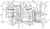
[0017] 도 1은 특정 애플리케이션들에 대해 기능-특정 벡터 프로세싱을 제공하는 것에 각각 전용된 다수의 벡터 프로세싱 엔진(VPE)들을 포함하는 예시적인 벡터 프로세서의 개략도이다.
[0018] 도 2는 별도의 VPE들을 제공할 필요 없이, VPE에 제공된 일반 회로 및 하드웨어가 다수의 애플리케이션들 또는 기술들에 대해 매우 효율적인 방식으로 특정 타입들의 벡터 동작들을 수행하기 위해 다중 모드들로 프로그래밍될 수 있도록, 프로그램 가능 데이터 경로 구성들을 가진 일반 VPE를 포함하는 예시적인 벡터 프로세서의 개략도이다.
[0019] 도 3은 도 2의 VPE에 제공된 예시적인 벡터 프로세싱 스테이지들의 개략도이고, 특정의 벡터 프로세싱 스테이지들은 프로그램 가능 데이터 경로 구성들을 가진 예시적인 벡터 프로세싱 블록들을 포함한다.
[0020] 도 4a는 도 2 및 도 3의 예시적인 벡터 프로세서에 포함된 프로그램 가능 데이터 경로 구성들을 가진 적어도 하나의 벡터 프로세싱 블록의 예시적인 벡터 프로세싱을 예시하는 흐름도이다.
[0021] 도 4b는 도 2 및 도 3의 예시적인 벡터 프로세서에 각각 프로그램 가능 데이터 경로 구성들을 가지며 상이한 벡터 프로세싱 스테이지들로 제공된 곱셈기 블록들 및 누산기 블록들의 예시적인 벡터 프로세싱을 예시하는 흐름도이다.
[0022] 도 5는 도 2 및 도 3의 VPE의 벡터 프로세싱 스테이지에 제공된 복수의 곱셈기 블록들의 보다 상세한 개략도이고, 복수의 곱셈기 블록들 각각은 프로그램 가능 데이터 경로 구성들을 가져서, 복수의 곱셈기 블록들은 특정하고, 상이한 타입들의 벡터 곱셈 동작들을 수행하기 위한 다중 모드들로 프로그래밍될 수 있다.
[0023] 도 6은 8 비트×8 비트 벡터 데이터 입력 샘플 세트들 및 16 비트×16 비트 벡터 데이터 입력 샘플 세트들에 대한 곱셈 동작들을 제공하도록 프로그램될 수 있는 프로그램 가능 데이터 경로 구성들을 가진 도 5의 복수의 곱셈기 블록들 중 하나의 곱셈기 블록의 내부 컴포넌트들의 개략도이다.
[0024] 도 7은 도 2 및 도 3의 VPE의 곱셈기 블록 및 누산기 블록의 일반화된 개략도이고, 누산기 블록은 캐리(carry) 전파를 감소시키기 위하여 리던던트 캐리-세이브(carry-save) 포맷을 이용하는 캐리-세이브 누산기 구조를 이용한다.
[0025] 도 8은 누산기 블록이 리던던트 캐리-세이브 포맷을 사용하여 특정하고, 상이한 타입들의 벡터 누산 동작들을 수행하기 위해 다수의 모드들로 프로그래밍될 수 있도록, 도 2 및 도 3의 VPE에 제공된 도 7의 누산기 블록의 예시적인 내부 컴포넌트들의 상세한 개략도이고, 누산기 블록은 프로그램 가능 데이터 경로 구성들을 가진다.
[0026] 도 9a는 듀얼 24 비트 누산기 모드를 제공하기 위하여 프로그래밍된 데이터 경로 구성들을 가진 도 8의 누산기 블록의 개략도이다.
[0027] 도 9b는 단일 40 비트 누산기 모드를 제공하기 위해 프로그래밍된 데이터 경로 구성들을 가진 도 8의 누산기 블록의 개략도이다.
[0028] 도 9c는 16 비트 캐리-세이브 가산기 다음 단일 24 비트 누산기 모드를 제공하기 위해 프로그래밍된 데이터 경로 구성들을 가진 도 8의 누산기 블록의 개략도이다.
[0029] 도 10은 프로그램 가능 데이터 경로 구성들을 가진 VPE를 포함하여, VPE 내 공통 회로 및 하드웨어가, 본원에 개시된 실시예들에 따라 별도의 VPE들을 제공하기 위한 요건 없이, 다수의 애플리케이션들 또는 기술들에 대해 매우 효율적인 방식으로 특정 타입들의 벡터 동작들을 수행하도록 설계된 전용 회로로서 동작하도록 프로그래밍될 수 있는 벡터 프로세서를 포함할 수 있는 예시적인 프로세서 기반 시스템 블록이다.[0017] FIG. 1 is a schematic diagram of an exemplary vector processor that includes multiple vector processing engines (VPEs) dedicated to providing function-specific vector processing for specific applications.
[0018] FIG. 2 illustrates a block diagram of a general-purpose circuit and hardware provided to the VPE, without the need to provide separate VPEs, to program in multiple modes to perform particular types of vector operations in a highly efficient manner for multiple applications or techniques. Lt; / RTI > is a schematic diagram of an exemplary vector processor including a generic VPE with programmable data path configurations.
[0019] FIG. 3 is a schematic diagram of exemplary vector processing stages provided in the VPE of FIG. 2, and certain vector processing stages include exemplary vector processing blocks with programmable data path arrangements.
[0020] FIG. 4A is a flow chart illustrating exemplary vector processing of at least one vector processing block having programmable data path arrangements included in the exemplary vector processor of FIGS. 2 and 3;
[0021] FIG. 4B is a flow chart illustrating exemplary vector processing of multiplier blocks and accumulator blocks provided with different vector processing stages, each having programmable data path configurations to the exemplary vector processor of FIGS. 2 and 3;
[0022] FIG. 5 is a more detailed schematic diagram of a plurality of multiplier blocks provided in the vector processing stage of the VPE of FIGS. 2 and 3, each of the plurality of multiplier blocks having programmable data path arrangements, And may be programmed with multiple modes for performing different types of vector multiply operations.
[0023] FIG. 6 is a block diagram of an embodiment of the present invention shown in FIG. 5 with programmable data path arrangements that can be programmed to provide multiply operations for 8 bit × 8 bit vector data input sample sets and 16 bit × 16 bit vector data input sample sets. Lt; / RTI > is a schematic diagram of the internal components of one of the multiplier blocks.
[0024] FIG. 7 is a generalized schematic diagram of a multiplier block and an accumulator block of the VPE of FIGS. 2 and 3, in which the accumulator block carries a carry using a redundant carry-save format to reduce carry propagation; - Use a save-accumulator structure.
[0025] FIG. 8 is a block diagram of an embodiment of the present invention, in which the accumulator block is specified using a redundant carry-save format, and the diagram provided in the VPEs of FIGS. 2 and 3, so that it can be programmed into multiple modes to perform different types of vector accumulation operations. 7 < / RTI > of the accumulator block, and the accumulator block has programmable data path arrangements.
[0026] FIG. 9A is a schematic diagram of the accumulator block of FIG. 8 with data path configurations programmed to provide a dual 24-bit accumulator mode.
[0027] FIG. 9b is a schematic diagram of the accumulator block of FIG. 8 with data path configurations programmed to provide a single 40-bit accumulator mode.
[0028] FIG. 9C is a schematic diagram of the accumulator block of FIG. 8 with data path configurations programmed to provide a single 24-bit accumulator mode followed by a 16-bit carry-save adder.
[0029] FIG. 10 is a flow chart illustrating a method of configuring a common circuit and hardware within a VPE, including a VPE with programmable data path arrangements, without the need to provide separate VPEs in accordance with the embodiments disclosed herein, Based system block that may include a vector processor that may be programmed to operate as a dedicated circuit designed to perform certain types of vector operations in a highly efficient manner with respect to the processor.
[0030] 이제 도시된 도면들을 참조하여, 본 개시의 몇몇 예시적인 실시예들이 설명된다. 단어 "예시적인"은 본원에서 "예, 예증, 또는 예시로서 역할을 하는" 것을 의미하기 위하여 사용된다. "예시적인"으로서 본원에 설명된 임의의 실시예는 반드시 다른 실시예들에 비해 바람직하거나 유리한 것으로 해석되지 않을 것이다.[0030] Referring now to the figures shown, several exemplary embodiments of the present disclosure are described. The word "exemplary" is used herein to mean "serving as an example, illustration, or illustration. &Quot; Any embodiment described herein as "exemplary " is not necessarily to be construed as preferred or advantageous over other embodiments.
[0031] 본원에 개시된 실시예들은 다중-모드 벡터 프로세싱을 제공하기 위한 프로그램 가능 데이터 경로 구성들을 가진 벡터 프로세싱 엔진(VPE)들을 포함한다. 관련된 벡터 프로세서들, 시스템들, 및 방법들은 또한 개시된다. 본원에 개시된 VPE들은 벡터 프로세싱 스테이지에 의해 실행되는 벡터 명령에 따라 벡터 데이터를 프로세싱하도록 구성된 적어도 하나의 벡터 프로세싱 스테이지를 포함한다. 각각의 벡터 프로세싱 스테이지는 실행되는 벡터 명령에 기초하여 벡터 데이터를 프로세싱하도록 구성된 하나 또는 그 초과의 벡터 프로세싱 블록들을 포함한다. 벡터 프로세싱 블록들의 비제한적 예들은 곱셈기들 및 누산기들이다. 벡터 프로세싱 블록들은 벡터 프로세싱 블록들의 데이터 경로 구성에 기초하여 상이한 모드들에서 상이한 타입들의 명령들에 대한 상이한 벡터 동작들을 제공할 수 있다. 벡터 프로세싱 블록들의 데이터 경로 구성들은 실행되는 특정 벡터 명령에 따라 상이한 모드들에서 특정 벡터 프로세싱 동작들을 제공하기 위해 벡터 데이터를 상이하게 프로세싱하도록 프로그램 가능하고 재프로그램(즉, 리와이어링됨(rewire)) 가능할 수 있다.[0031] The embodiments disclosed herein include vector processing engines (VPEs) with programmable data path arrangements for providing multi-mode vector processing. Related vector processors, systems, and methods are also disclosed. The VPEs disclosed herein include at least one vector processing stage configured to process vector data in accordance with a vector instruction executed by a vector processing stage. Each vector processing stage includes one or more vector processing blocks configured to process vector data based on the vector instructions being executed. Non-limiting examples of vector processing blocks are multipliers and accumulators. The vector processing blocks may provide different vector operations for different types of instructions in different modes based on the data path configuration of the vector processing blocks. The data path arrangements of the vector processing blocks are programmable and reprogrammed (i.e., rewired) to process the vector data differently to provide specific vector processing operations in different modes according to the particular vector instruction being executed. It can be possible.
[0032] 이런 방식으로, VPE는 실행되는 벡터 명령에 따라 상이한 타입들의 벡터 동작들을 실행하기 위해 재프로그램 가능한 자신의 데이터 경로 구성들을 가질 수 있다. 결과적으로, 보다 적은 VPE들은 벡터 프로세서에서 원해진 벡터 프로세싱 동작들을 제공할 수 있고, 따라서 스칼라 프로세싱 엔진들에 비해 더 적은 레지스터 기록들 및 보다 빠른 벡터 명령 실행 시간들의 벡터 프로세싱 장점들을 여전히 유지하면서 벡터 프로세서의 영역이 절약된다. 벡터 프로세싱 블록들에 대한 데이터 경로 구성들은 또한 VPE에서 상이한 모드들의 상이하고, 특정된 벡터 동작들의 실행을 지원하기 위하여 VPE에서 벡터 명령 실행 동안 프로그래밍되고 재프로그래밍될 수 있다.[0032] In this way, the VPE may have its own data path configurations reprogrammable to perform different types of vector operations according to the vector instructions being executed. As a result, fewer VPEs can provide the desired vector processing operations in the vector processor, and thus, with fewer register writes and vector processing advantages of faster vector instruction execution times compared to scalar processing engines, Is saved. The data path configurations for the vector processing blocks may also be programmed and reprogrammed during vector instruction execution in the VPE to support the execution of different and specified vector operations of the different modes in the VPE.
[0033] 본원에 개시된 다중-모드 벡터 프로세싱을 위한 프로그램 가능 데이터 경로 구성들을 가진 VPE들은 고정된 기능들을 제공하기 위하여 단지 고정된 데이터 경로 구성들만을 포함하는 VPE들과 차이를 나타낸다. 본원에 개시된 벡터 프로세싱을 위한 프로그램 가능 데이터 경로 구성들을 가진 VPE들은 또한 예를 들어 디지털 신호 프로세서(DSP)들에 제공된 것들 같은 스칼라 프로세싱 엔진들과 차이를 나타낸다. 스칼라 프로세싱 엔진들은 상이한 타입들의 비고정된 기능들을 수행할 뿐 아니라, 벡터 명령 실행 동안 중간 결과들을 레지스터 파일들에 기록하기 위해 융통성 있는 일반 회로 및 논리를 이용하고, 이에 의해 부가적인 전력을 소비하고 벡터 명령 실행 횟수들을 증가시킨다.[0033] VPEs with programmable data path configurations for multi-mode vector processing disclosed herein differ from VPEs that include only fixed data path configurations to provide fixed functions. VPEs with programmable data path configurations for vector processing disclosed herein also differ from scalar processing engines such as those provided in, for example, digital signal processors (DSPs). The scalar processing engines not only perform non-fixed functions of different types, but also use flexible general circuitry and logic to write intermediate results to register files during vector instruction execution, thereby consuming additional power, Increase the number of command executions.
[0034] 이에 관하여, 도 2는 또한 벡터 프로세싱 엔진(VPE)(22)이라 지칭되는 예시적인 벡터 프로세싱 유닛(22)을 포함하는 기저대역 프로세서(20)의 개략도이다. 기저대역 프로세서(20) 및 그의 VPE(22)는 반도체 다이(24)에 제공될 수 있다. 이 실시예에서, 도 3에서 시작하여 하기 더 상세히 논의될 바와 같이, 기저대역 프로세서(20)는 프로그램 가능 데이터 경로 구성들을 가진 일반 VPE(22)를 포함한다. 이런 방식으로, VPE(22)는 기저대역 프로세서(20)에 별도의 VPE들을 제공하기 위한 요건 없이 상이한 동작 모드들에서 상이한 특정 타입들의 벡터 동작들을 제공하기 위해 프로그래밍 및 재프로그래밍될 수 있는 일반 회로 및 하드웨어를 포함한다. VPE(22)는 또한, 기저대역 프로세서(20)에 별도의 VPE들을 제공하기 위한 요건 없이, 다수의 애플리케이션들 또는 기술들에 대해 매우 효율적인 방식으로 일반 산술 동작들을 수행하기 위해 벡터 산술 모드로 프로그래밍될 수 있다.[0034] In this regard, FIG. 2 is also a schematic diagram of a
[0035] 도 3에서 시작하는 벡터 다중-모드 프로세싱을 위해 VPE(22)에 제공된 프로그램 가능 데이터 경로 구성들을 논의하기 전에, 도 2의 기저대역 프로세서(20)의 컴포넌트들이 먼저 설명된다. 이런 비제한적 예에서 기저대역 프로세서(20)는 512 비트 벡터 프로세서이다. 기저대역 프로세서(20)는 기저대역 프로세서(20)에서 벡터 프로세싱을 제공하는 VPE(22)를 지원하기 위하여 VPE(22)에 더하여 부가적인 컴포넌트들을 포함한다. 기저대역 프로세서(20)는 벡터 유닛 데이터 메모리(LMEM)(32)로부터의 벡터 데이터(30)를 수신 및 저장하기 위해 구성된 벡터 레지스터들(28)을 포함한다. 예를 들어, 벡터 데이터(30)는 X 비트 폭이고, 'X'는 설계 선택(예를 들어, 512 비트들)에 따라 정의된다. 벡터 데이터(30)는 벡터 데이터 샘플 세트들(34)로 나누어질 수 있다. 예를 들어, 벡터 데이터(30)는 256 비트 폭일 수 있고 보다 작은 벡터 데이터 샘플 세트들(34(Y)-34(0))을 포함할 수 있고, 여기서 벡터 데이터 샘플 세트들(34(Y)-34(0))의 몇몇은 16 비트 폭이고, 벡터 데이터 샘플 세트들(34(Y)-34(0))의 다른 것들은 32 비트 폭이다. VPE(22)는 높은 병렬도를 달성하기 위하여 VPE(22)에 병렬로 제공된 특정 선택된 곱셈 벡터 데이터 샘플 세트들(34(Y)-34(0))에 대해 벡터 프로세싱을 제공할 수 있다. 벡터 레지스터들(28)은 또한, VPE(22)가 벡터 데이터(30)를 프로세싱할 때 생성된 결과들을 저장하도록 구성된다. 특정 실시예들에서, VPE(22)는 보다 빠른 벡터 명령 실행 시간들을 제공하기 위하여 레지스터 기록들을 감소시키기 위해 중간 벡터 프로세싱 결과들을 벡터 레지스터들(28)에 저장하지 않도록 구성된다. 이 구성은 스칼라 프로세싱 DSP들 같은 레지스터들에 중간 결과들을 저장하는 스칼라 프로세싱 엔진들에 의해 실행되는 스칼라 명령들과 반대이다.[0035] Before discussing the programmable data path configurations provided to the
[0036] 도 2의 기저대역 프로세서(20)는 또한 벡터 명령들의 조건적 실행에 사용하기 위해 조건들을 VPE(22)에 제공하고 업데이트된 조건들을 벡터 명령 실행의 결과로서 저장하도록 구성된 조건 레지스터들(36)을 포함한다. 기저대역 프로세서(20)는 또한 누산 레지스터들(38), 글로벌 레지스터들(40), 및 어드레스 레지스터들(42)을 포함한다. 누산 레지스터들(38)은 벡터 데이터(30)에 대한 특정 특정된 동작들을 실행한 결과로서 누산된 결과들을 저장하기 위해 VPE(22)에 의해 사용되도록 구성된다. 글로벌 레지스터들(40)은 VPE(22)에 의해 지원된 특정 벡터 명령들에 대한 스칼라 오퍼랜드(operand)들을 저장하도록 구성된다. 어드레스 레지스터들(42)은 벡터 로드에 의해 어드레스 가능한 어드레스들을 저장하고, 벡터 유닛 데이터 메모리(32)로부터 벡터 데이터(30)를 리트리브하고 벡터 유닛 데이터 메모리(32)에 벡터 프로세싱 결과들을 저장하기 위해 VPE(22)에 의해 지원된 명령들을 저장하도록 구성된다.The
[0037] 도 2를 계속 참조하여, 이 실시예에서 기저대역 프로세서(20)는 또한 VPE(22)에 의해 제공된 벡터 프로세싱에 더하여 기저대역 프로세서(20)에서 스칼라 프로세싱을 제공하기 위해 스칼라 프로세서(44)(또한 "정수 유닛"으로 지칭됨)를 포함한다. 매우 효율적인 동작을 위해 실행된 명령 타입에 기초하여 벡터 및 스칼라 명령 동작들 둘 다를 지원하도록 구성된 CPU를 제공하는 것이 원해질 수 있다. 이 실시예에서, 스칼라 프로세서(44)는 비제한적인 예로서 32 비트 축소 명령 집합 컴퓨팅(RISC: reduced instruction set computing) 스칼라 프로세서이다. 스칼라 프로세서(44)는 이 예에서 스칼라 명령 프로세싱을 지원하기 위해 산술 논리 유닛(ALU)(46)을 포함한다. 기저대역 프로세서(20)는 프로그램 메모리(50)로부터 명령들을 인출하고, 인출된 명령들을 디코딩하고, 그리고 명령 타입에 기초하여 인출된 명령들을 스칼라 프로세서(44)에 보내거나 벡터 데이터 경로(49)를 VPE(22)로 보내도록 구성된 명령 디스패치 회로(48)를 포함한다. 스칼라 프로세서(44)는 스칼라 명령들을 실행할 때 스칼라 프로세서(44)에 의해 사용하기 위한 범용 레지스터들(52)을 포함한다. 정수 유닛 데이터 메모리(DMEM: integer unit data meM0ry)(54)는 스칼라 명령 실행을 위한 스칼라 프로세서(44)에 의해 액세스하기 위한 데이터를 메인 메모리로부터 범용 레지스터들(52)로 제공하기 위해 기저대역 프로세서(20)에 포함된다. DMEM(54)은 비제한적 예로서 캐시 메모리일 수 있다. 기저대역 프로세서(20)는 또한, 스칼라 프로세서(44)가 메모리 제어기 데이터 경로들(59)을 통해 메인 메모리에 액세스를 요구하는 벡터 명령들을 실행할 때 범용 레지스터들(52)로부터 메모리 어드레스들을 수신하도록 구성된 메모리 제어기 레지스터들(58)을 포함하는 메모리 제어기(56)를 포함한다.[0037] Still referring to Figure 2, in this embodiment, the
[0038] 도 2의 기저대역 프로세서(20)의 예시적인 컴포넌트들이 설명되었기 때문에, 일반 회로 및 하드웨어로 동작의 다중 모드들을 제공하는 VPE(22) 및 이의 프로그램 가능 데이터 경로 구성들에 관한 보다 상세한 것은 이제 논의된다. 이에 관하여, 도 3은 도 2의 VPE(22)의 예시적인 개략도를 예시한다. 도 3에 예시되고 도 4-도 8c에서 하기에 더 상세히 설명될 바와 같이, VPE(22)는 프로그램 가능 데이터 경로 구성들로 구성될 수 있는 예시적인 벡터 프로세싱 블록들을 가진 복수의 예시적인 벡터 프로세싱 스테이지들(60)을 포함한다. 하기에 보다 상세히 논의될 바와 같이, 벡터 프로세싱 블록들에 제공된 프로그램 가능 데이터 경로 구성들은 특정 회로들 및 하드웨어가 도 2의 벡터 유닛 데이터 메모리(32)로부터 수신된 벡터 데이터(30)에 대해 상이하고, 특정한 벡터 프로세싱 동작들을 수행하는 것을 지원하도록 프로그래밍 및 재프로그래밍되게 한다.[0038] Since the exemplary components of the
[0039] 예를 들어, 특정 벡터 프로세싱 동작들은 보통 벡터 데이터(30)의 곱셈 다음 곱셈된 벡터 데이터 결과들의 누산을 요구할 수 있다. 그런 벡터 프로세싱의 비제한적 예들은 필터링 동작들, 상관 동작들, 및 무선 통신 알고리즘을 위한 고속 푸리에 변환(FFT) 동작을 수행하기 위하여 보통 사용되는 Radix-2 및 Radix-4 버터플라이(butterfly) 동작들을 포함하고, 여기서 일련의 병렬 곱셈들은 제공되고 그 다음 곱셈 결과들의 일련의 병렬 누산들이 제공된다. 또한 도 7-도 9c에 관하여 하기 보다 상세히 논의될 바와 같이, 도 2의 VPE(22)는 또한 캐리-세이브 누산기들에 리던던트 캐리-세이브 포맷을 제공하기 위하여 캐리-세이브 누산기들을 가진 융합 곱셈기들의 옵션을 가진다. 캐리-세이브 누산기들에 리던던트-절약 포맷을 제공하는 것은 각각의 누산 단계 동안 캐리 전파 경로 및 캐리 전파 가산 동작을 제공할 필요를 제거할 수 있다.[0039] For example, certain vector processing operations may require the accumulation of the
[0040] 이에 관하여, 도 3을 추가로 참조하여, VPE(22)의 M0 곱셈 벡터 프로세싱 스테이지(60(1))는 먼저 설명될 것이다. M0 곱셈 벡터 프로세싱 스테이지(60(1))는 각각 프로그램 가능 데이터 경로 구성들을 가진 임의의 원해진 수의 곱셈기 블록들(62(A)-62(0)) 형태의 복수의 벡터 프로세싱 블록들을 포함하는 제 2 벡터 프로세싱 스테이지이다. 곱셈기 블록들(62(A)-62(0))은 VPE(22)에서 벡터 곱셈 동작들을 수행하기 위해 제공된다. 복수의 곱셈기 블록들(62(A)-62(0))은 최대 열두 개(12) 곱셈 벡터 데이터 샘플 세트들(34(Y)-34(0))의 곱셈을 제공하기 위해 M0 곱셈 벡터 프로세싱 스테이지(60(1))에서 서로 병렬로 배치된다. 이 실시예에서, 'A'는 세 개(3)와 동일하고, 이는 네 개(4)의 곱셈기 블록들(62(3)-62(0))이 이 예에서 M0 곱셈 벡터 프로세싱 스테이지(60(1))에 포함되는 것을 의미한다. 곱셈 벡터 데이터 샘플 세트들(34(Y)-34(0))은 VPE(22)의 제 1 벡터 프로세싱 스테이지(60(0))인 입력 판독(RR) 벡터 프로세싱 스테이지에 제공된 복수의 래치들(64(Y)-64(0))에 벡터 프로세싱을 위해 VPE(22)에 로딩된다. 이 실시예에서 VPE(22)에 열두 개(12) 래치들(64(11)-64(0))이 있고, 이는 이 실시예에서 'Y'가 열한 개(11)와 동일하다는 것을 의미한다. 래치들(64(11)-64(0))은 벡터 레지스터들(28)(도 2 참조)로부터 리트리브된 곱셈 벡터 데이터 샘플 세트들(34(11)-34(0))을 벡터 데이터 입력 샘플 세트들(66(11)-66(0))로서 래치하도록 구성된다. 이 예에서, 각각의 래치(64(11)-64(0))는 8 비트 폭이다. 래치들(64(11)-64(0))은 벡터 데이터(30)의 총 96 비트 폭(즉, 각각 12 래치들×8 비트들)에 대해, 곱셈 벡터 데이터 입력 샘플 세트들(66(11)-66(0))을 래치하도록 각각 개별적으로 구성된다.[0040] In this regard, with further reference to FIG. 3, the MO multiplication vector processing stage 60 (1) of the
[0041] 도 3을 계속 참조하여, 복수의 곱셈기 블록들(62(3)-62(0))은 벡터 곱셈 동작들을 제공하기 위하여 벡터 데이터 입력 샘플 세트들(66(11)-66(0))의 특정 결합들을 수신할 수 있도록 구성되고, 여기서 'Y'는 이 예에서 열한 개(11)와 동일하다. 곱셈 벡터 데이터 입력 샘플 세트들(66(11)-66(0))은 VPE(22)의 설계에 따라 복수의 입력 데이터 경로들(A3-A0, B3-B0, 및 C3-C0)에 제공된다. 벡터 데이터 입력 샘플 세트들(66(3)-66(0))은 도 3에 예시된 바와 같이 입력 데이터 경로들(C3-C0)에 대응한다. 벡터 데이터 입력 샘플 세트들(66(7)-66(4))은 도 3에 예시된 바와 같이 입력 데이터 경로들(B3-B0)에 대응한다. 벡터 데이터 입력 샘플 세트들(66(11)-66(8))은 도 3에 예시된 바와 같이 입력 데이터 경로들(A3-A0)에 대응한다. 복수의 곱셈기 블록들(62(3)-62(0))은 벡터 곱셈 동작들을 제공하기 위하여, 개별적으로 복수의 곱셈기 블록들(62(3)-62(0))에 제공된 입력 데이터 경로들(A3-A0, B3-B0, C3-C0)에 따라 수신된 벡터 데이터 입력 샘플 세트들(66(11)-66(0))을 프로세싱하도록 구성된다.3, a plurality of multiplier blocks 62 (3) -62 (0) are coupled to the vector data input sample sets 66 (11) -66 (0) ), Where 'Y' is the same as eleven (11) in this example. The multiplication vector data input sample sets 66 (11) -66 (0) are provided to a plurality of input data paths A3-A0, B3-B0, and C3-C0 according to the design of the
[0042] 도 4 및 도 5에 관하여 하기 보다 상세히 논의될 바와 같이, 도 3의 곱셈기 블록들(62(3)-62(0))에 제공된 프로그램 가능 내부 데이터 경로들(67(3)-67(0))은 상이한 데이터 경로 구성들을 가지도록 프로그래밍될 수 있다. 이들 상이한 데이터 경로 구성들은 각각의 곱셈기 블록(62(3)-62(0))에 제공된 특정 입력 데이터 경로들(A3-A0, B3-B0, C3-C0)에 따라 곱셈기 블록들(62(3)-62(0))에 제공된 특정 수신된 벡터 데이터 입력 샘플 세트들(66(11)-66(0))의 곱셈의 상이한 결합들 및/또는 상이한 비트 길이들을 제공한다. 이에 관하여, 복수의 곱셈기 블록들(62(3)-62(0))은 벡터 곱셈 출력 샘플 세트들(68(3)-68(0))을, 벡터 데이터 입력 샘플 세트들(66(11)-66(0))의 특정 결합을 곱셈한 것의 곱셈 결과를 포함하는 벡터 결과 출력 샘플 세트로서 함께 제공한다.As discussed in greater detail below with respect to FIGS. 4 and 5, the programmable internal data paths 67 (3) -67 (3) -62 (0) provided in the multiplier blocks 62 (0) may be programmed to have different data path configurations. These different data path arrangements are multiplied by multiplier blocks 62 (3) -62 (0) according to the specific input data paths (A3-A0, B3-B0, C3-C0) provided in each multiplier block 62 ) -62 (0)) of the received vector data sample sets 66 (11) -66 (0) and / or different bit lengths. In this regard, a plurality of multiplier blocks 62 (3) -62 (0) are coupled to the vector multiplication output sample sets 68 (3) -68 (0) -66 (0)). ≪ / RTI >
[0043] 예를 들어, 곱셈기 블록들(62(3)-62(0))의 프로그램 가능 내부 데이터 경로들(67(3)-67(0))은 도 2의 기저대역 프로세서(20)의 명령 디스패치(48)의 벡터 명령 디코더로부터 제공된 세팅들에 따라 프로그래밍될 수 있다. 이 실시예에서, 곱셈기 블록들(62(3)-62(0))의 네 개(4)의 프로그램 가능 내부 데이터 경로들(67(3)-67(0))이 있다. 벡터 명령은 VPE(22)에 의해 수행될 특정 타입의 동작을 특정한다. 따라서, VPE(22)는 매우 효율적인 방식으로 동일한 일반 회로를 상이한 타입들의 벡터 곱셈 동작들에 제공하기 위해 곱셈기 블록들(62(3)-62(0))의 프로그램 가능 내부 데이터 경로들(67(3)-67(0))을 구성하도록 프로그래밍 및 재프로그래밍될 수 있다. 예를 들어, VPE(22)는 명령 디스패치(48)의 명령 파이프라인에서 벡터 명령들의 디코딩에 따라, 실행된 각각의 벡터 명령에 대한 단위 클록 사이클에 기초하여 곱셈기 블록들(62(3)-62(0))의 프로그램 가능 내부 데이터 경로들(67(3)-67(0))을 구성 및 재구성하도록 프로그래밍될 수 있다. 따라서, 만약 VPE(22)의 M0 곱셈 벡터 프로세싱 스테이지(60(1))가 매 클록 사이클마다 벡터 데이터 입력 샘플 세트들(66)을 프로세싱하도록 구성되면, 결과로서, 곱셈기 블록들(62(3)-62(0))은 명령 디스패치(48)의 명령 파이프라인에서 벡터 명령들의 디코딩에 따라 매 클록 사이클 상에서 벡터 곱셈 동작들을 수행한다.For example, the programmable internal data paths 67 (3) -67 (0) of the multiplier blocks 62 (3) -62 (0) May be programmed in accordance with the settings provided from the vector instruction decoder of the
[0044] 곱셈기 블록들(62)은 실수 및 복소수 곱셈들을 수행하도록 프로그래밍될 수 있다. 도 3을 계속 참조하여, 하나의 벡터 프로세싱 블록 데이터 경로 구성에서, 곱셈기 블록(62)은 두 개의 8 비트 벡터 데이터 입력 샘플 세트들(66)을 함께 곱셈하도록 구성될 수 있다. 하나의 곱셈 블록 데이터 경로 구성에서, 곱셈기 블록(62)은, 제 1 쌍의 8 비트 벡터 데이터 입력 샘플 세트들(66) 곱하기 제 2 쌍의 8 비트 벡터 데이터 입력 샘플 세트들(66)로부터 형성되는, 두 개의 16 비트 벡터 데이터 입력 샘플 세트들(66)을 함께 곱셈하도록 구성될 수 있다. 이것은 도 6에 예시되고 하기 보다 상세히 논의된다. 다시, 곱셈기 블록들(62(3)-62(0))에 프로그램 가능 데이터 경로 구성들을 제공하는 것은, 곱셈기 블록들(62(3)-62(0))이 VPE(22) 영역을 감소시키고 아마도 보다 적은 VPE(22)들이 원해진 벡터 프로세싱 동작들을 수행하기 위해 기저대역 프로세서(20)에 제공되게 하도록 상이한 타입들의 곱셈 동작들을 수행하도록 구성 및 재구성될 수 있다는 점에서 융통성을 제공한다.[0044] The multiplier blocks 62 may be programmed to perform real and complex multiplications. With continued reference to FIG. 3, in one vector processing block data path configuration, the
[0045] 도 3을 다시 참조하여, 복수의 곱셈기 블록들(62(3)-62(0))은 프로그램 가능 출력 데이터 경로들(70(3)-70(0))의 벡터 곱셈 출력 샘플 세트들(68(3)-68(0))을 다음 벡터 프로세싱 스테이지(60) 또는 출력 프로세싱 스테이지에 제공하도록 구성된다. 벡터 곱셈 출력 샘플 세트들(68(3)-68(0))은 복수의 곱셈기 블록들(62(3)-62(0))에 의해 실행되는 벡터 명령에 기초하여 프로그래밍된 구성에 따라 프로그램 가능 출력 데이터 경로들(70(3)-70(0))에 제공된다. 이 예에서, 프로그램 가능 출력 데이터 경로들(70(3)-70(0))의 벡터 곱셈 출력 샘플 세트들(68(3)-68(0))은 하기 논의될 바와 같이 누산을 위해 M1 누산 벡터 프로세싱 스테이지(60(2))에 제공된다. VPE(22)의 이 특정 설계에서, 벡터 데이터 입력들의 곱셈들 다음 곱셈된 결과들의 누산을 요구하는 특정 벡터 명령들을 지원하기 위해 복수의 곱셈기 블록들(62(3)-62(0)) 다음 누산기들을 제공하는 것이 원해진다. 예를 들어, FFT 동작을 제공하기 위하여 보통 사용되는 Radix-2 및 Radix-4 버터플라이 동작들은 일련의 곱셈 동작들 다음 곱셈 결과들의 누산을 포함한다. 그러나, VPE(22)에 제공된 벡터 프로세싱 블록들의 결합들이 예시적이고 비제한적인 것이 주의된다. 프로그램 가능 데이터 경로 구성들을 가진 VPE는 벡터 프로세싱 블록들을 가진 하나 또는 임의의 다른 수의 벡터 프로세싱 스테이지들을 포함하도록 구성될 수 있다. 벡터 프로세싱 블록들은 VPE에 의해 지원되도록 설계된 설계 및 특정 벡터 명령들에 따라 임의의 타입의 동작들을 수행하도록 제공될 수 있다.Referring again to FIG. 3, a plurality of multiplier blocks 62 (3) -62 (0) is coupled to a vector multiplication output sample set 70 (3) of the programmable output data paths 70 (68 (3) -68 (0)) to the next
[0046] 도 3을 계속 참조하여, 이 실시예에서, 벡터 곱셈 출력 샘플 세트들(68(3)-68(0))은 M1 누산 벡터 프로세싱 스테이지(60(2))인 다음 벡터 프로세싱 스테이지에 제공된 복수의 누산기 블록들(72(3)-72(0))에 제공된다. 복수의 누산기 블록들(72(A)-72(0)) 중 각각의 누산기 블록은 두 개의 누산기들(72(X)(1) 및 72(X)(0))(즉, 72(3)(1), 72(3)(0), 72(2)(1), 72(2)(0), 72(1)(1), 72(1)(0), 및 72(0)(1), 72(0)(0))을 포함한다. 복수의 누산기 블록들(72(3)-72(0))은 벡터 곱셈 출력 샘플 세트들(68(3)-68(0))의 결과들을 누산한다. 도 7-도 9c에 관하여 하기 보다 상세히 논의될 바와 같이, 복수의 누산기 블록들(72(3)-72(0))은 캐리-세이브 누산기들로서 제공될 수 있고, 캐리 산물(product)은, 누산 동작이 완료될 때까지 누산 프로세스 동안 필수적으로 절약되고 전파되지 않는다. 복수의 누산기 블록들(72(3)-72(0))은 또한 복수의 누산기 블록들(72(3)-72(0))의 리던던트 캐리-세이브 포맷을 제공하기 위하여 도 4 및 도 5의 복수의 곱셈기 블록들(62(3)-62(0))과 융합되는 옵션을 가진다. 복수의 누산기 블록들(72(3)-72(0))에 리던던트 캐리-세이브 포맷을 제공하는 것은 복수의 누산기 블록들(72(3)-72(0))에서 누산의 각각의 단계 동안 캐리 전파 경로 및 캐리 전파 가산 동작을 제공할 필요를 제거할 수 있다. M1 누산 벡터 프로세싱 스테이지(60(2)) 및 이의 복수의 누산기 블록들(72(3)-72(0))은 이제 도 3을 참조하여 도입될 것이다.Still referring to FIG. 3, in this embodiment, the vector multiplication output sample sets 68 (3) -68 (0) are stored in the next vector processing stage which is the M1 accumulation vector processing stage 60 (2) And provided to a plurality of provided accumulator blocks 72 (3) to 72 (0). Each accumulator block of the plurality of accumulator blocks 72 (A) -72 (0) includes two accumulators 72 (X) (1) and 72 (X) (1), 72 (3) (0), 72 (2), 72 (2) (0), 72 (1), 72 (1) 1), 72 (0) (0). The plurality of accumulator blocks 72 (3) -72 (0) accumulates the results of the vector multiplication output sample sets 68 (3) -68 (0). A plurality of accumulator blocks 72 (3) -72 (0) may be provided as carry-save accumulators, and a carry product may be provided as carry- It is not necessarily saved and propagated during the accumulation process until the operation is completed. A plurality of accumulator blocks 72 (3) -72 (0) are also used to provide a redundant carry-save format of the plurality of accumulator blocks 72 (3) -72 And has an option to be fused with a plurality of multiplier blocks 62 (3) -62 (0). Providing a redundant carry-save format to the plurality of accumulator blocks 72 (3) -72 (0) results in a carry in each accumulator block 72 (3) -72 (0) It is possible to eliminate the need to provide the propagation path and carry propagation operation. The M1 accumulation vector processing stage 60 (2) and its multiple accumulator blocks 72 (3) -72 (0) will now be introduced with reference to FIG.
[0047] 도 3을 참조하여, M1 누산 벡터 프로세싱 스테이지(60(2))의 복수의 누산기 블록들(72(3)-72(0))은, 다음 벡터 프로세싱 스테이지(60) 또는 출력 프로세싱 스테이지에 누산기 출력 샘플 세트들(76(3)-76(0))(즉, 76(3)(1), 76(3)(0), 76(2)(1), 76(2)(0), 76(1)(1), 76(1)(0), 및 76(0)(1), 76(0)(0))을 제공하기 위하여, 프로그램 가능 출력 데이터 경로 구성들에 따라, 프로그램 가능 출력 데이터 경로들(74(3)-74(0))(즉, 74(3)(1), 74(3)(0), 74(2)(1), 74(2)(0), 74(1)(1), 74(1)(0), 및 74(0)(1), 74(0)(0))에서 벡터 곱셈 출력 샘플 세트들(68(3)-68(0))을 누산하도록 구성된다. 이 예에서, 누산기 출력 샘플 세트들(76(3)-76(0))은 ALU 프로세싱 스테이지(60(3))인 출력 프로세싱 스테이지에 제공된다. 예를 들어, 하기 보다 상세히 논의되는 바와 같이, 누산기 출력 샘플 세트들(76(3)-76(0))은 또한 비제한적 예로서, 도 2의 기저대역 프로세서(20)의 스칼라 프로세서(44)의 ALU(46)에 제공될 수 있다. 예를 들어, ALU(46)는 보다 일반적 프로세싱 동작들에 사용될 VPE(22)에 의해 실행되는 특정 벡터 명령들에 따라 누산기 출력 샘플 세트들(76(3)-76(0))을 취할 수 있다.3, a plurality of accumulator blocks 72 (3) -72 (0) of the M1 accumulation vector processing stage 60 (2) are coupled to the next
[0048] 도 3을 다시 참조하여, 누산기 블록들(72(3)-72(0))의 프로그램 가능 입력 데이터 경로들(78(3)-78(0)) 및/또는 프로그램 가능 내부 데이터 경로들(80(3)-80(0))은 곱셈기 블록들(62(3)-62(0))로부터 누산기 블록들(72(3)-72(0))로 제공된 벡터 곱셈 출력 샘플 세트들(68(3)-68(0))의 상이한 결합들 및/또는 비트 길이들을 수신하기 위해 재구성되도록 프로그래밍될 수 있다. 각각의 누산기 블록(72)이 두 개의 누산기들(72(X)(1), 72(X)(0))로 구성되기 때문에, 프로그램 가능 입력 데이터 경로들(78(A)-78(0))은 도 3에 78(3)(1), 78(3)(0), 78(2)(1), 78(2)(0), 78(1)(1), 78(1)(0), 및 78(0)(1), 78(0)(0)로서 도시된다. 유사하게, 프로그램 가능 내부 데이터 경로들(80(3)-80(A))은 도 3에 80(3)(1), 80(3)(0), 80(2)(1), 80(2)(0), 80(1)(1), 80(1)(0), 80(0)(1), 80(0)(0)로서 도시된다. 누산기 블록들(72(3)-72(0))에 프로그램 가능 입력 데이터 경로들(78(3)-78(0)) 및/또는 프로그램 가능 내부 데이터 경로들(80(3)-80(0))을 제공하는 것은 도 8-도 9c에 관하여 하기에 보다 상세히 논의된다. 이런 방식으로, 누산기 블록들(72(3)-72(0))의 프로그램 가능 입력 데이터 경로들(78(3)-78(0)) 및/또는 프로그램 가능 내부 데이터 경로들(80(3)-80(0))에 따라, 누산기 블록들(73(2)-72(0))은 누산된 벡터 곱셈 출력 샘플 세트들(68(3)-68(0))의 프로그래밍된 결합에 따라 누산기 출력 샘플 세트들(76(3)-76(0))을 제공할 수 있다. 다시, 이것은 누산기 블록들(72(3)-72(0))이, VPE(22)의 면적을 감소시키고 아마도 보다 적은 VPE(22)들이 원해진 벡터 프로세싱 동작들을 수행하기 위하여 기저대역 프로세서(20)에 제공되게 허용하기 위하여 프로그램 가능 입력 데이터 경로들(78(3)-78(0)) 및/또는 프로그램 가능 내부 데이터 경로들(80(3)-80(0))의 프로그래밍에 기초하여 상이한 타입들의 누산 동작들을 수행하도록 구성 및 재구성될 수 있다는 점에서 융통성을 제공한다.Referring again to FIG. 3, the programmable input data paths 78 (3) -78 (0) of the accumulator blocks 72 (3) -72 (0) and / (3) -80 (0) are provided from the multiplier blocks 62 (3) -62 (0) to the vector multiplication output sample sets May be programmed to reconfigure to receive different combinations of bits 68 (3) -68 (0) and / or bit lengths. Since each
[0049] 예를 들어, 하나의 누산기 모드 구성에서, 두 개의 누산기 블록들(72)의 프로그램 가능 입력 데이터 경로(78) 및/또는 프로그램 가능 내부 데이터 경로들(80)은 비제한 예로서 단일 40 비트 누산기를 제공하도록 프로그래밍될 수 있다. 이것은 도 9a에 예시되고 하기에 보다 상세히 논의된다. 다른 누산기 모드 구성에서, 두 개의 누산기 블록들(72)의 프로그램 가능 입력 데이터 경로(78) 및/또는 프로그램 가능 내부 데이터 경로(80)는 비제한 예로서 듀얼 24 비트 누산기들을 제공하도록 프로그래밍될 수 있다. 이것은 도 9b에 예시되고 하기에 더 상세히 논의된다. 다른 누산기 모드 구성에서, 두 개의 누산기 블록들(72)의 프로그램 가능 입력 데이터 경로(78) 및/또는 프로그램 가능 내부 데이터 경로(80)는 16 비트 캐리-세이브 가산기 다음 단일 24 비트 누산기를 제공하도록 프로그래밍될 수 있다. 이것은 도 9c에 예시되고 하기에 더 상세히 논의된다. 곱셈들 및 누산 동작들의 특정 상이한 결합들은 또한 곱셈기 블록들(62(3)-62(0)) 및 누산기 블록들(72(3)-72(0))(예를 들어, 16 비트 누산과 16 비트 복소수 곱셈, 및 16 비트 누산과 32 비트 복소수 곱셈)의 프로그래밍에 따라 VPE(22)에 의해 지원될 수 있다.For example, in one accumulator mode configuration, the programmable
[0050] 누산기 블록들(72(3)-72(0))의 프로그램 가능 입력 데이터 경로들(78(3)-78(0)) 및/또는 프로그램 가능 내부 데이터 경로들(80(3)-80(0))은 도 2의 기저대역 프로세서(20)의 명령 디스패치(48)의 벡터 명령 디코더로부터 제공된 세팅들에 따라 프로그래밍될 수 있다. 벡터 명령은 VPE(22)에 의해 수행될 특정 타입의 동작을 특정한다. 따라서, VPE(22)는 명령 디스패치(48)의 명령 파이프로라인에서 벡터 명령의 디코딩에 따라 실행되는 각각의 벡터 명령 동안 누산기 블록들(72(3)-72(0))의 프로그램 가능 입력 데이터 경로들(78(3)-78(0)) 및/또는 프로그램 가능 내부 데이터 경로들(80(3)-80(0))을 재프로그래밍하도록 구성될 수 있다. 벡터 명령은 VPE(22)의 하나 또는 그 초과의 클록 사이클들에 걸쳐 실행할 수 있다. 또한 이 예에서, VPE(22)는 단위 클록 사이클에 기초하여 벡터 명령의 각각의 클록 사이클 동안 누산기 블록들(72(3)-72(0))의 프로그램 가능 입력 데이터 경로들(78(3)-78(0)) 및/또는 프로그램 가능 내부 데이터 경로들(80(3)-80(0))을 재프로그래밍하도록 구성될 수 있다. 따라서, 예를 들어, VPE(22)의 M1 누산 벡터 프로세싱 스테이지(60(2))에 의해 실행된 벡터 명령이 매 클록 사이클 마다 벡터 곱셈 출력 샘플 세트들(68(3)-68(0))을 프로세싱하면, 결과로서, 누산기 블록들(72(3)-72(0))의 프로그램 가능 입력 데이터 경로들(78(3)-78(0)) 및/또는 프로그램 가능 내부 데이터 경로들(80(3)-80(0))은 벡터 명령의 실행 동안 각각의 클록 사이클에서 재구성될 수 있다.The programmable input data paths 78 (3) -78 (0) and / or programmable internal data paths 80 (3) - 72 (0) of the accumulator blocks 72 80 (0) may be programmed in accordance with the settings provided from the vector instruction decoder of the
[0051] 도 4a 및 도 4b는 예시적인 벡터 프로세싱의 많은 예시를 제공하기 위하여 도 2 및 도 3의 VPE(22)의 곱셈기 블록들(62(A)-62(0)) 및 누산기 블록들(72(A)(1)-72(0)(0))의 예시적인 벡터 프로세싱을 예시하는 흐름도들이다. 도 4a는 도 2 및 도 3의 예시적인 VPE에 포함된 프로그램 가능 데이터 경로 구성들을 가진, 곱셈기 블록들(62(A)-62(0)), 누산기 블록들(72(A)(1)-72(0)(0)) 또는 둘 다일 수 있는 일반화된 벡터 프로세싱 블록의 예시적인 벡터 프로세싱을 예시하는 흐름도이다. 도 4b는 도 2 및 도 3의 예시적인 VPE(22)에서 프로그램 가능 데이터 경로 구성들을 각각 가지며 상이한 벡터 프로세싱 스테이지들에 제공된 곱셈기 블록들(62(A)-62(0)) 및 누산기 블록들(72(A)(1)-72(0)(0))의 예시적인 벡터 프로세싱을 예시하는 흐름도이다.[0051] Figures 4A and 4B illustrate the multiplier blocks 62 (A) -62 (0) and accumulator blocks (A) -62 (0) of the
[0052] 이에 관하여, 도 4a에 예시된 바와 같이, VPE(22)의 프로세스는 입력 프로세싱 스테이지(60(0))의 복수의 입력 데이터 경로들(A3-C0) 중 하나의 입력 데이터 경로에서 벡터 어레이의 폭의 복수의 벡터 데이터 입력 샘플 세트들(34(Y)-34(0))을 수신하는 것(블록 81)을 포함한다. 다음 벡터 프로세싱은 벡터프로세싱 블록들(62(A)-62(0) 및/또는 72(A)(1)-72(0)(0))의 복수의 입력 데이터 경로들(A3-C0)로부터 벡터 데이터 입력 샘플 세트들(34(Y)-34(0))을 수신(블록 83)하는 것을 포함한다. 다음 벡터 프로세싱은 벡터 프로세싱 스테이지(60(1), 60(2))에 의해 실행된 벡터 명령에 따라 벡터 프로세싱 블록들(62(A)-62(0), 72(A)(1)-72(0)(0))에 대한 프로그램 가능 데이터 경로 구성들(67(A)-67(0), 70(3)-70(0), 78(A)(1)-78(0)(0), 80(A)(1)-80(0)(0), 74(A)(1)-74(0)(0))에 기초하여 벡터 결과 출력 샘플 세트들(68(A)-68(0), 76(A)(1)-76(0)(0))을 제공하기 위하여 벡터 데이터 입력 샘플 세트들(34(Y)-34(0))을 프로세싱하는 것(블록 85)을 포함한다. 다음 벡터 프로세싱은 출력 데이터 경로들(70(A)-70(0), 74(A)(1)-74(0)(0))에서 벡터 결과 출력 샘플 세트들(68(A)-68(0), 76(A)(1)-76(0)(0))을 제공하는 것(블록 87)을 포함한다. 다음 벡터 프로세싱은 출력 프로세싱 스테이지(60(3))에서 벡터 프로세싱 스테이지(60(1), 60(2))로부터 벡터 결과 출력 샘플 세트들(68(A)-68(0), 76(A)(1)-76(0)(0))을 수신하는 것(블록 89)을 포함한다.In this regard, as illustrated in FIG. 4A, the process of the
[0053] 도 4a에 관하여 상기 설명된 벡터 프로세싱에서 각각의 프로세싱 스테이지(60(0)-60(3))가 병렬 벡터 프로세싱을 위해 동시에 발생하는 것이 주의되고, 여기서 벡터 프로세싱 블록들(62(A)-62(0), 72(A)(1)-72(0)(0))의 프로그램 가능 데이터 경로 구성들(67(A)-67(0), 70(3)-70(0), 78(A)(1)-78(0)(0), 80(A)(1)-80(0)(0), 74(A)(1)-74(0)(0))은 각각의 클록 사이클만큼 자주 재프로그래밍될 수 있다. 상기 논의된 바와 같이, 이것은 벡터 프로세싱 블록들(62(A)-62(0), 72(A)(1)-72(0)(0))이 상이한 벡터 명령들에 대한 상이한 동작들을 일반 벡터 프로세싱 블록들(62(A)-62(0), 72(A)(1)-72(0)(0))의 사용을 통해 효율적으로 수행하게 한다.It should be noted that in the vector processing described above with reference to FIG. 4a, each of the processing stages 60 (0) -60 (3) occur simultaneously for parallel vector processing, where the vector processing blocks 62 (A 70 (3) -70 (0)) of the programmable data path configurations 67 (A) - 67 (0), 72 (A) , 78 (A) (1) -78 (0) (0), 80 (A) (1) -80 (0), 74 (A) Can be reprogrammed as often as each clock cycle. As discussed above, this allows vector processing blocks 62 (A) -62 (0), 72 (A) (1) -72 (0) To be efficiently performed through the use of processing blocks 62 (A) -62 (0), 72 (A) (1) -72 (0) (0).
[0054] 도 4b는 곱셈 동작들 다음 누산 동작들을 수반하는 벡터 명령들 동안 도 3의 VPE(22)의 곱셈기 블록들(62(A)-62(0)) 및 누산기 블록들(72(A)(1)-72(0)(0))의 예시적인 벡터 프로세싱을 예시하는 흐름도이다. 예를 들어, FFT 벡터 동작들은 곱셈 동작들 다음 누산 동작들을 수반한다. 도 4b의 흐름도는 도 4a에서 상기 설명된 VPE(22)의 예시적인 일반화된 벡터 프로세싱의 예시적인 상세를 추가로 제공한다. 이에 관하여, 벡터 프로세싱은 입력 프로세싱 스테이지(60(0))에서 복수의 입력 데이터 경로들(A3-C0) 중 하나의 입력 데이터 경로에서 벡터 어레이의 폭의 복수의 벡터 데이터 입력 샘플 세트들(34(Y)-34(0))을 수신하는 것(블록 93)을 수반한다. 그 다음 벡터 프로세싱은 복수의 곱셈기 블록들(62(A)-62(0))의 복수의 입력 데이터 경로들(A3-C0)로부터 벡터 데이터 입력 샘플 세트들(34(Y)-34(0))을 수신하는 것(블록 95)을 포함한다. 그 다음 벡터 프로세싱은 벡터 프로세싱 스테이지(60(1))에 의해 실행된 벡터 명령에 따른 곱셈기 블록들(62(A)-62(0))에 대한 프로그램 가능 데이터 경로 구성들(67(A)-67(0), 70(3)-70(0))에 기초하여, 복수의 곱셈 출력 데이터 경로들(70(A)-70(0)) 중 곱셈 출력 데이터 경로들(70(A)-70(0))에서 곱셈 벡터 결과 출력 샘플 세트들(68(A)-68(0))을 제공하기 위해 벡터 데이터 입력 샘플 세트들(34(Y)-34(0))을 곱셈하는 것(블록 97)을 포함한다. 다음 벡터 프로세싱은 복수의 누산기 블록들(72(A)(1)-72(0)(0))의 복수의 곱셈 출력 데이터 경로들(70(A)-70(0))로부터 곱셈 벡터 결과 출력 샘플 세트들(68(A)-68(0))을 수신하는 것(블록 99)을 포함한다. 다음 벡터 프로세싱은 제 2 벡터 프로세싱 스테이지(60(2))에 의해 실행된 벡터 명령에 따른 누산기 블록들(72(A)(1)-72(0)(0))에 대한 프로그램 가능 데이터 경로(78(A)(1)-78(0)(0), 80(A)(1)-80(0)(0), 74(A)(1)-74(0)(0)) 구성들에 기초하여 벡터 누산 결과 샘플 세트들(76(A)(1)-76(0)(0))을 제공하기 위해 곱셈 벡터 결과 출력 샘플 세트들(68(A)-68(0))을 함께 누산하는 것(블록 101)을 포함한다. 그 다음 벡터 프로세싱은 출력 데이터 경로들(74(A)(1)-74(0)(0))에 벡터 누산 결과 샘플 세트들(76(A)(1)-76(0)(0))을 제공하는 것(블록 103)을 포함한다. 그 다음 벡터 프로세싱은 출력 프로세싱 스테이지(60(3))의 누산기 블록들(72(A)(1)-72(0)(0))로부터 벡터 결과 출력 샘플 세트들(76(A)(1)-76(0)(0))을 수신하는 것(블록 105)을 포함한다.[0054] Figure 4B illustrates the multiplier blocks 62 (A) -62 (0) and the accumulator blocks 72 (A) of the
[0055] 프로그램 가능 데이터 경로 구성들을 가진 벡터 프로세싱 블록들을 이용하는 도 3의 예시적인 VPE(22) 및 도 4a 및 도 4b의 벡터 프로세싱의 개요가 설명되었기 때문에, 설명의 나머지는 도 5-도 9c의 이들 벡터 프로세싱 블록들의 보다 예시적인 비제한적 상세들을 설명한다.[0055] Since the
[0056] 이에 관하여, 도 5는 도 3의 VPE(22)의 M0 곱셈 벡터 프로세싱 스테이지(60(1))의 복수의 곱셈기 블록들(62(3)-62(0))의 보다 상세한 개략도이다. 도 6은 도 5의 곱셈기 블록(62)의 내부 컴포넌트들의 개략도이다. 도 5에 예시된 바와 같이, 특정 입력 데이터 경로들(A3-A0, B3-B0, C3-C0)에 따라 곱셈기 블록들(62(3)-62(0))에 의해 수신된 벡터 데이터 입력 샘플 세트들(66(11)-66(0))은 도시된다. 도 6에 관하여 하기에 보다 상세히 논의될 바와 같이, 이 예에서 곱셈기 블록들(62(3)-62(0)) 각각은 네 개(4)의 8 비트×8 비트 곱셈기들을 포함한다. 도 5를 다시 참조하여, 이 예에서 곱셈기 블록들(62(3)-62(0)) 각각은 피승수 입력 'B' 또는 피승수 입력 'C'에 의해 피승수 입력 'A'를 곱셈하도록 구성된다. 곱셈기 블록(62)에서 함께 곱셈될 수 있는 피승수 입력들 'A' 및 'B' 또는 'C'는 제어되고 이에 의해 도 5에 도시된 바와 같이, 입력 데이터 경로들(A3-A0, B3-B0, C3-C0)이 곱셈기 블록들(62(3)-62(0))에 연결된다. 피승수 선택기 입력(82(3)-82(0))은, 피승수 입력 'B' 또는 피승수 입력 'C' 중 어느 것이 피승수 입력 'A'에 의해 곱셈 되도록 선택되는지를 선택하기 위해 각각의 곱셈기 블록(62(3)-62(0))의 프로그램 가능 내부 데이터 경로들(67(3)-67(0))을 제어하기 위하여 각각의 곱셈기 블록(62(3)-62(0))에 입력으로서 제공된다. 이런 방식으로, 곱셈기 블록들(62(3)-62(0))은 원해진 바와 같이 상이한 곱셈 동작들을 제공하기 위해 자신의 프로그램 가능 내부 데이터 경로들(67(3)-67(0))이 재프로그래밍될 능력을 가진다.5 is a more detailed schematic diagram of a plurality of multiplier blocks 62 (3) -62 (0) of the M0 multiply vector processing stage 60 (1) of the
[0057] 도 5를 계속 참조하여, 예로서 곱셈기 블록(62(3))을 사용하여, 입력 데이터 경로들(A3 및 A2)은 개별적으로 입력들(AH 및 AL)에 연결된다. 입력(AH)은 피승수 입력 A의 하이(high) 비트들을 나타내고, AL은 입력 피승수 입력 'A'의 로우(low) 비트들을 의미한다. 입력 데이터 경로들(B3 및 B2)은 개별적으로 입력들(BH 및 BL)에 연결된다. 입력(BH)은 하이 비트들의 피승수 입력 'B'을 나타내고 AL은 입력 피승수 입력 'B'의 로우 비트들을 나타낸다. 입력 데이터 경로들(C3 및 C2)는 개별적으로 입력들(CI 및 CQ)에 연결된다. 입력(CI)은 이 예에서 입력 피승수 입력 'C'의 실수 비트 부분을 나타낸다. CQ는 이 예에서 입력 피승수 입력 'C'의 허수 비트 부분을 나타낸다. 도 6에 관하여 하기 보다 상세히 논의될 바와 같이, 피승수 선택기 입력(82(3))은 또한, 곱셈기 블록(62(3))의 프로그램 가능 내부 데이터 경로들(67(3))이 피승수 입력 'B' 또는 피승수 입력 'C' 중 어느 것과 피승수 입력 'A'에 대해 8 비트 곱셈을 수행하도록 구성되는지, 또는 곱셈기 블록(62(3))이 이 예에서 피승수 입력 'B' 또는 피승수 입력 'C' 중 어느 것과 피승수 입력 'A'에 대해 16 비트 곱셈을 수행하도록 구성되는지를 제어한다.[0057] With continued reference to FIG. 5, using the multiplier block 62 (3) as an example, input data paths A3 and A2 are individually connected to inputs AH and AL. The input (AH) represents the high bits of the multiplicand input A and the AL represents the low (low) bits of the input multiplicand input 'A'. The input data paths B3 and B2 are individually connected to the inputs BH and BL. The input (BH) represents the multiplicand input 'B' of the high bits and the AL represents the low bits of the input multiplicand input 'B'. The input data paths C3 and C2 are individually connected to inputs CI and CQ. The input (CI) represents the real bit portion of the input multiplicand input 'C' in this example. CQ represents the imaginary bit portion of the input multiplicand input 'C' in this example. The multiplicand selector input 82 (3) also includes a programmable internal data path 67 (3) of the multiplier block 62 (3), as will be discussed in greater detail below with respect to Figure 6, Multiplier block 62 (3) is configured to perform either an multiplicand input 'B' or a multiplicand input 'C' in this example, And a 16-bit multiplication for the multiplicand input 'A'.
[0058] 도 5를 계속 참조하여, 곱셈기 블록들(62(3)-62(0))은 자신의 프로그램 가능 내부 데이터 경로들(67(3)-67(0))의 구성에 기초하여 곱셈 동작의 캐리 'C' 및 합 'S' 벡터 출력 샘플 세트들로서 벡터 곱셈 출력 샘플 세트들(68(3)-68(0))을 각각 생성하도록 구성된다. 도 7-도 9c에 관하여 하기 더 상세히 논의될 바와 같이, 벡터 곱셈 출력 샘플 세트들(68(3)-68(0))의 캐리 'C' 및 합 'S'는 융합되고, 이는 캐리 'C' 및 합 'S'이 복수의 누산기들(72(3)-72(0))에 리던던트 캐리-세이브 포맷을 제공하기 위해 복수의 누산기들(72(3)-72(0))에 리던던트 캐리-세이브 포맷으로 제공되는 것을 의미한다. 하기 더 상세히 논의될 바와 같이, 복수의 누산기들(72(3)-72(0))에 리던던트 캐리-세이브 포맷을 제공하는 것은 복수의 누산기들(72(3)-72(0))에 의해 수행되는 누산 동작들 동안 캐리 전파 경로 및 캐리 전파 가산 동작을 제공할 필요를 제거할 수 있다.[0058] With continued reference to FIG. 5, multiplier blocks 62 (3) -62 (0) are operable to perform multiplication based on the configuration of their programmable internal data paths 67 (3) -67 (0) To generate vector multiplication output sample sets 68 (3) -68 (0), respectively, as the carry 'C' of operation and sum 'S' vector output sample sets. The carry 'C' and sum 'S' of the vector multiplication output sample sets 68 (3) -68 (0) are fused, as will be discussed in more detail below with respect to Figures 7-9C, (0)) to a plurality of accumulators 72 (3) -72 (0) to provide a redundant carry-save format to the plurality of accumulators 72 (3) - means to be provided in save format. Providing a redundant carry-save format to a plurality of accumulators 72 (3) -72 (0), as will be discussed in greater detail below, is accomplished by a plurality of accumulators 72 (3) -72 (0) It is possible to eliminate the need to provide a carry propagation path and carry propagation operation during the accumulation operations being performed.
[0059] 자신의 프로그램 가능 내부 데이터 경로들(67(3)-67(0))의 구성에 기초하여 벡터 곱셈 출력 샘플 세트들(68(3)-68(0))을 곱셈 동작의 캐리 'C' 및 합 'S' 벡터 출력 샘플 세트들로서 생성하는 곱셈기 블록들(62(3)-62(0))의 예들은 도 5에 도시된다. 예를 들어, 곱셈기 블록(62(3))은 캐리 C00 및 합 S00을 8 비트 곱셈들에 대한 32 비트 값들로서 생성하고 캐리 C01 및 합 S01을 16 비트 곱셈들에 대한 64 비트 값들로서 생성하도록 구성된다. 다른 곱셈기 블록들(62(2)-62(0))은 이 예에서 동일한 능력을 가진다. 이에 관하여, 곱셈기 블록(62(2))은 캐리 C10 및 합 S10을 8 비트 곱셈들에 대해 32 비트 값들로서 생성하고 캐리 C11 및 합 S11을 16 비트 곱셈들에 대한 64 비트 값들로서 생성하도록 구성된다. 곱셈기 블록(62(1))은 캐리 C20 및 합 S20을 8 비트 곱셈들에 대한 32 비트 값들로서 생성하고 캐리 C21 및 합 S21을 16 비트 곱셈들에 대한 64 비트 값들로서 생성하도록 구성된다. 곱셈기 블록(62(0))은 캐리 C30 및 합 S30을 8 비트 곱셈들에 대한 32 비트 값들로서 생성하고 캐리 C31 및 합 S31을 16 비트 곱셈들에 대한 64 비트 값들로서 생성하도록 구성된다.Based on the configuration of its own programmable internal data paths 67 (3) -67 (0), the vector multiplication output sample sets 68 (3) -68 (0) Examples of multiplier blocks 62 (3) -62 (0) generating as C 'and sum' S 'vector output sample sets are shown in FIG. For example, multiplier block 62 (3) may be configured to generate carry C00 and sum S00 as 32-bit values for 8-bit multiplications and carry C01 and sum S01 as 64-bit values for 16-bit multiplications do. The other multiplier blocks 62 (2) -62 (0) have the same capability in this example. In this regard, multiplier block 62 (2) is configured to generate carry C10 and sum S10 as 32-bit values for 8-bit multiplications and carry C11 and sum S11 as 64-bit values for 16-bit multiplications . The multiplier block 62 (1) is configured to generate carry C20 and sum S20 as 32-bit values for 8-bit multiplications and carry C21 and sum S21 as 64-bit values for 16-bit multiplications. The multiplier block 62 (0) is configured to generate carry C30 and sum S30 as 32-bit values for 8-bit multiplications and carry C31 and sum S31 as 64-bit values for 16-bit multiplications.
[0060] 도 5의 곱셈기 블록(62)에 제공된 프로그램 가능 데이터 경로 구성들의 더 많은 예시적인 상세를 설명하기 위하여, 도 6이 제공된다. 도 6은 8 비트×8 비트 벡터 데이터 입력 샘플 세트(66)를 곱셈하고, 16 비트×16 비트 벡터 데이터 입력 샘플 세트(66)를 곱셈할 수 있는 프로그램 가능 데이터 경로 구성들을 가진 도 3 및 도 4의 곱셈기 블록(62)의 내부 컴포넌트들의 개략도이다. 이에 관하여, 곱셈기 블록(62)은 이 예에서 4개의 8×8 비트 곱셈기들(84(3)-84(0))을 포함한다. 임의의 원해진 수의 곱셈기들(84)이 제공될 수 있다. 제 1 곱셈기(84(3))는 8 비트 벡터 데이터 입력 샘플 세트(66A[H])(이것은 입력 피승수 입력 'A'의 하이 비트들임)를 수신하고 벡터 데이터 입력 샘플 세트(66A[H])를 8 비트 벡터 데이터 입력 샘플 세트(66B[H])(이것은 입력 피승수 입력 'B'의 하이 비트들임) 또는 8 비트 벡터 데이터 입력 샘플 세트(66C[I])(이것은 입력 피승수 입력 'C'의 하이 비트들임) 어느 하나와 곱셈하도록 구성된다. 곱셈기(84(3))에 피승수로서 제공되는 것인 8 비트 벡터 데이터 입력 샘플 세트(66B[H]) 또는 8 비트 벡터 데이터 입력 샘플 세트(66C[I]) 중 어느 하나를 선택하도록 구성된 멀티플렉서(86(3))가 제공된다. 멀티플렉서(86(3))는 이 실시예에서 피승수 선택기 입력(82)에 하이 비트인 피승수 선택기 비트 입력(82[3])에 의해 제어된다. 이런 방식으로, 멀티플렉서(86(3)) 및 피승수 선택기 비트 입력(82[3])은, 8 비트 벡터 데이터 입력 샘플 세트(66B[H]) 또는 8 비트 벡터 데이터 입력 샘플 세트(66C[I]) 중 어느 것이 수신 벡터 데이터 입력 샘플 세트(66A[H])와 곱셈 되는지를 제어하기 위하여 곱셈기(84(3))에 대한 프로그램 가능 내부 데이터 경로(67[0]) 구성을 제공한다.[0060] To illustrate more exemplary details of the programmable data path arrangements provided in the
[0061] 도 6을 계속 참조하여, 다른 곱셈기들(84(2)-84(0))은 또한 제 1 곱셈기(84(3))에 대해 제공된 바와 같이 유사한 프로그램 가능 내부 데이터 경로들(67[2]-67[0])을 포함한다. 곱셈기(84(2))는 피승수 입력 'A'의 로우 비트들인 8 비트 벡터 데이터 입력 샘플 세트(66A[L])와 곱셈될 8 비트 벡터 데이터 입력 샘플 세트(66B[H]) 또는 7 비트 벡터 데이터 입력 샘플 세트(66C[I])를 프로그램 가능 내부 데이터 경로(67[1])에 제공할 프로그램 가능 구성을 가진 프로그램 가능 내부 데이터 경로(67[2])를 포함한다. 선택은 이 실시예에서 피승수 선택기 입력(82)에서 피승수 선택기 비트 입력(82[2])에 따라 멀티플렉서(86(2))에 의해 제어된다. 곱셈기(84(1))는 8 비트 벡터 데이터 입력 샘플 세트(66A[H])와 곱셈될, 피승수 입력 'B'의 로우 비트들인 8 비트 벡터 데이터 입력 샘플 세트(66B[L]) 또는 피승수 입력 'C'의 로우 비트들인 8 비트 벡터 데이터 입력 샘플 세트(66C[Q])를 프로그램 가능 내부 데이터 경로(67[1])에 제공하기 위하여 프로그램 가능한 프로그램 가능 내부 데이터 경로(67[1])를 포함한다. 선택은 이 실시예에서 피승수 선택기 입력(82)의 피승수 선택기 비트 입력(82[1])에 따라 멀티플렉서(86(1))에 의해 제어된다. 게다가, 곱셈기(84(0))는 8 비트 벡터 데이터 입력 샘플 세트[66A[L])와 곱셈될, 8 비트 벡터 데이터 입력 샘플 세트(66B[L]) 또는 8 비트 벡터 데이터 입력 샘플 세트(66C[Q])를 프로그램 가능 내부 데이터 경로(67[0])에 제공하기 위하여 프로그램 가능한 프로그램 가능 내부 데이터 경로(67[0])를 포함한다. 선택은 이 실시예에서 피승수 선택기 입력(82)의 피승수 선택기 비트 입력(82[0])에 따라 멀티플렉서(86(0))에 의해 제어된다.6, other multipliers 84 (2) -84 (0) are also coupled to similar programmable internal data paths 67 [3] as provided for first multiplier 84 (3) 2] -67 [0]). The multiplier 84 (2) multiplies the 8 bit vector data input sample set 66B [H] to be multiplied by the 8 bit vector data input sample set 66A [L], which is the low bits of the multiplicand input 'A' And a programmable internal data path 67 [2] having a programmable configuration for providing a data input sample set 66C [I] to the programmable internal data path 67 [1]. The selection is controlled by the multiplexer 86 (2) in accordance with the multiplicand selector bit input 82 [2] in the
[0062] 도 6을 계속 참조하여, 상기 논의된 바와 같이, 곱셈기들(84(3)-84(0))은 상이한 비트 길이 곱셈 동작들을 수행하도록 구성될 수 있다. 이에 관하여, 각각의 곱셈기(84(3)-84(0))는 비트 길이 곱셈 모드 입력들(88(3)-88(0))을 개별적으로 포함한다. 이 예에서, 각각의 곱셈기(84(3)-84(0))는 프로그램 가능 데이터 경로들(90(3)-90(0), 91 및 92(3)-92(0))의 구성을 개별적으로 제어하는 입력들에 따라 8 비트×8비트 모드에서 프로그래밍될 수 있다. 각각의 곱셈기(84(3)-84(0))는 또한, 프로그램 가능 데이터 경로들(90(3)-90(0), 91 및 92(3)-92(0))의 구성을 개별적으로 제어하는 입력들에 따라, 16 비트×16 비트 모드 및 24 비트×8비트 모드를 포함하는 보다 큰 비트 곱셈 동작의 부분을 제공하도록 프로그래밍될 수 있다. 예를 들어, 각각의 곱셈기(84(3)-84(0))가 프로그램 가능 데이터 경로들(90(3)-90(0))의 구성에 따라 8 비트×8비트 곱셈 모드로 구성되면, 유닛으로서 복수의 곱셈기들(84(3)-84(0))은 곱셈기 블록(62)의 부분으로 두 개(2)의 개별 8 비트×8 비트 곱셈기들을 포함하도록 구성될 수 있다. 각각의 곱셈기(84(3)-84(0))가 프로그램 가능 데이터 경로(91)의 구성에 따라 16 비트×16 비트 곱셈 모드로 구성되면, 유닛으로서 복수의 곱셈기들(84(3)-84(0))은 곱셈기 블록(62)의 부분으로서 단일 16 비트×16 비트 곱셈기를 포함하도록 구성될 수 있다. 곱셈기들(84(3)-84(0))이 프로그램 가능 데이터 경로들(92(3)-92(0))의 구성에 따라 24 비트×8 비트 곱셈 모드로 구성되면, 유닛으로서 복수의 곱셈기들(84(3)-84(0))은 곱셈기 블록(62)의 부분으로 하나(1)의 16 비트×24 비트×8 비트 곱셈기를 포함하도록 구성될 수 있다.[0062] With continued reference to FIG. 6, multipliers 84 (3) -84 (0) may be configured to perform different bit length multiply operations, as discussed above. In this regard, each multiplier 84 (3) -84 (0) individually includes bit length multiplication mode inputs 88 (3) -88 (0). In this example, each multiplier 84 (3) -84 (0) has a configuration of programmable data paths 90 (3) -90 (0), 91 and 92 (3) -92 Can be programmed in an 8-bit by 8-bit mode depending on the individually controlled inputs. Each of the multipliers 84 (3) -84 (0) also has the configuration of the programmable data paths 90 (3) -90 (0), 91 and 92 (3) -92 May be programmed to provide portions of a larger bit-multiply operation, including 16-bit by 16-bit mode and 24-bit by 8-bit mode, depending on the inputs to control. For example, if each multiplier 84 (3) -84 (0) is configured in an 8-bit x 8-bit multiplication mode according to the configuration of programmable data paths 90 (3) -90 (0) A plurality of multipliers 84 (3) -84 (0) as a unit may be configured to include two (2) separate 8-bit x 8-bit multipliers as part of
[0063] 도 6을 계속 참조하여, 이 예에서 곱셈기들(84(3)-84(0))은 16 비트×16 비트 곱셈 모드로 구성되는 것으로 도시된다. 열 여섯(16)-비트 입력 합들(94(3), 94(2)) 및 입력 캐리들(96(3), 96(2))은 개별적으로 각각의 곱셈기(84(3), 84(2))에 의해 생성된다. 열 여섯(16) 비트 입력 합들(94(1), 94(0)) 및 입력 캐리들(96(1), 96(0))은 개별적으로 각각의 곱셈기(84(1), 84(0))에 의해 생성된다. 16 비트 입력 합들(94(3), 94(2)) 및 입력 캐리들(96(3), 96(2))은 또한 입력 합들(94(3)-94(0)) 및 입력 캐리들(96(3)-96(0))을 함께 가산하기 위하여 16 비트 합 입력(94(1), 94(0)) 및 입력 캐리들(96(1), 96(0))과 함께 24 비트 4:2 압축기(109)에 제공된다. 가산된 입력 합들(94(3)-94(0)) 및 입력 캐리들(96(3)-96(0))은, 프로그램 가능 데이터 경로(91)가 액티브이고 입력 합들(94(3)-94(0)) 및 입력 캐리들(96(3)-96(0))이 게이팅될 때 16 비트×16 비트 곱셈 모드로 단일 합(98) 및 단일 캐리(100)를 제공한다. 프로그램 가능 데이터 경로(91)는 24 비트 4:2 압축기(109)에 제공되도록 제 1 AND 기반 게이트(102(3))에 의해 16 비트 워드로서 결합된 입력 합들(94(3), 94(2)), 및 제 2 AND 기반 게이트(102(2))에 의해 16 비트 워드로서 결합된 입력 캐리들(96(3), 96(2))이 게이팅된다. 프로그램 가능 데이터 경로(91)는 또한 24 비트 4:2 압축기(109)에 제공되도록 제 3 AND 기반 게이트(102(1))에 의해 16 비트 워드로서 결합된 입력 합들(94(1), 94(0)), 및 제 4 AND 기반 게이트(102(0))에 의해 16 비트 워드로서 결합된 입력 캐리들(96(1), 96(0))이 게이팅된다. 프로그램 가능 출력 데이터 경로(70[0])는, 곱셈기 블록(62)이 16 비트×16 비트 또는 24 비트×8 비트 곱셈 모드로 구성되면, 압축된 32 비트 합(S0) 및 32 비트 캐리(C0) 부분 적으로서 벡터 곱셈 출력 샘플 세트(68[0])가 제공된다.[0063] Still referring to FIG. 6, multipliers 84 (3) -84 (0) in this example are shown to be configured in a 16-bit by 16-bit multiplication mode. The sixteen (16) -bit input sums 94 (3) and 94 (2) and the input carries 96 (3) and 96 (2) )). The sixteen (16) bit input sums 94 (1) and 94 (0) and the input carries 96 (1) and 96 (0) ). The 16-bit input sums 94 (3) and 94 (2) and the input carries 96 (3) and 96 (2) (1), 96 (0)) together with the 16-bit sum inputs 94 (1) and 94 (0) and the input carries 96 (1) and 96 : 2 compressor (109). The additive input sums 94 (3) -94 (0) and input carries 96 (3) -96 (0) Provides a
[0064] 프로그램 가능 출력 데이터 경로(70[1]) 구성은, 만약 곱셈기 블록(62) 내 곱셈기들(84(3)-84(0))이 8 비트×8 비트 곱셈 모드로 구성되면, 압축 없이 부분 산물들로서 16 비트 입력 합들(94(3)-94(0)) 및 대응하는 16 비트 입력 캐리들(96(3)-96(0))로서 제공된다. 프로그램 가능 출력 데이터 경로(70[1])는 만약 곱셈기 블록(62) 내 곱셈기들(84(3)-84(0))이 8 비트×8 비트 곱셈 모드로 구성되면 압축 없이 벡터 곱셈 출력 샘플 세트들(68[1])로서 16 비트 입력 합들(94(3)-94(0)) 및 대응하는 16 비트 입력 캐리들(96(3)-96(0))로서 제공된다. 곱셈기 블록(62)의 곱셈 모드에 따라 벡터 곱셈 출력 샘플 세트들(68[0], 68[1])은 실행되는 벡터 명령에 따라 합 및 캐리 산물들의 누산을 위해 누산기 블록들(72(3)-72(0))에 제공된다.The configuration of the programmable output data path 70 [1] is such that if the multipliers 84 (3) -84 (0) in the
[0065] 프로그램 가능 데이터 경로 구성들을 가진 도 4 및 도 5의 곱셈기 블록들(62(3)-62(0))이 설명되었기 때문에, 리던던트 캐리-세이브 포맷으로 구성된 누산기 블록들(72(3)-72(0))과 융합될 VPE(22)의 곱셈기 블록들(62(3)-62(0))의 피처들은 이제 도 7에 관하여 일반적으로 설명될 것이다.Since the multiplier blocks 62 (3) -62 (0) of Figures 4 and 5 with programmable data path configurations have been described, the accumulator blocks 72 (3) configured in the redundant carry- The features of the multiplier blocks 62 (3) -62 (0) of the
[0066] 이에 관하여, 도 7은 도 2 및 도 3의 VPE의 곱셈기 블록 및 누산기 블록의 일반화된 개략도이고, 누산기 블록은 캐리 전파를 감소시키기 위하여 리던던트 캐리-세이브 포맷을 이용하는 캐리-세이브 누산기 구조를 이용한다. 이전에 논의되고 도 7에 예시된 바와 같이, 곱셈기 블록들(62)은 피승수 입력들(66[H] 및 66[L])을 곱셈하고 프로그램 가능 출력 데이터 경로(70)에서 벡터 곱셈 출력 샘플 세트들(68)로서 적어도 하나의 입력 합(94) 및 적어도 하나의 입력 캐리(96)를 제공하도록 구성된다. 각각의 누산 단계 동안 누산기 블록(72)에서 캐리 전파 경로 및 캐리 전파 가산기를 제공할 필요를 제거하기 위해, 프로그램 가능 출력 데이터 경로(70)에서 벡터 곱셈 출력 샘플 세트들(68)의 적어도 하나의 입력 합(94) 및 적어도 하나의 입력 캐리(96)는 리던던트 캐리 절약 포맷으로 적어도 하나의 누산기 블록(72)에 융합된다. 다른 말로, 벡터 곱셈 출력 샘플 세트들(68)의 캐리(96)는 캐리 절약 포맷의 벡터 입력 캐리(96)로서 누산기 블록(72)에 제공된다. 이런 방식으로, 벡터 곱셈 출력 샘플 세트들(68)의 입력 합(94) 및 입력 캐리(96)는 이 실시예에서 복소수 게이트 4:2 압축기인 누산기 블록(72)의 압축기(108)에 제공될 수 있다. 압축기(108)는 개별적으로 이전 누산된 벡터 출력 합(112) 및 이전 시프트된 누산 벡터 출력 캐리(117)와 함께 입력 합(94) 및 입력 캐리(96)를 누산하도록 구성된다. 이전 시프트된 누산 벡터 출력 캐리(117)는 필수적으로 누산 동작 동안 절약된 캐리 누산이다.In this regard, FIG. 7 is a generalized schematic diagram of a multiplier block and an accumulator block of the VPE of FIGS. 2 and 3, and the accumulator block includes a carry-save accumulator structure using a redundant carry-save format to reduce carry propagation . As previously discussed and illustrated in FIG. 7, multiplier blocks 62 multiply multiplicand inputs 66 [H] and 66 [L] and outputs a vector multiplication output sample set As
[0067] 이런 방식으로, 단지 단일, 최종 캐리 전파 가산기만이 누산기 블록(72)에 의해 생성된 누산의 부분으로서 수신된 입력 캐리(96)를 입력 합(94)에 전파하기 위해 누산기 블록(72)에 제공되도록 요구되지 않는다. 누산기 블록(72)에서 각각의 누산 단계 동안 캐리 전파 가산 동작을 수행하는 것과 연관된 전력 소비는 이 실시예에서 감소된다. 또한 누산기 블록(72)에서 각각의 누산 단계 동안 캐리 전파 가산 동작을 수행하는 것과 연관된 게이트 지연은 또한 이 실시예에서 제거된다. In this manner, only a single, final carry wave adder is coupled to the accumulator block 72 (not shown) to propagate the received carry 96 to the
[0068] 도 7을 계속 참조하여, 압축기(108)는 개별적으로 이전 누산된 벡터 출력 합(112) 및 이전 시프트된 누산 벡터 출력 캐리(117)와 리던던트 형태로 입력 합(94) 및 입력 캐리(96)를 누산하도록 구성된다. 시프트된 누산 벡터 출력 캐리(117)는, 다음 수신된 입력 합(94) 및 입력 캐리(96)의 다음 누산이 압축기(108)에 의해 수행되기 전에, 누산된 벡터 출력 캐리(114)를 시프팅함으로써 압축기(108) 비트에 의해 생성된 누산된 벡터 출력 캐리(114)에 의해 생성된다. 최종 시프트된 누산 벡터 출력 캐리(117)는 누산기 블록(72)에 제공된 단일, 최종 캐리 전파 가산기(119)에 의해 최종 누산 벡터 출력 합(112)에 가산되고, 누산기 블록(72)은 최종 누산 벡터 출력 합(112)을 최종 누산기 출력 샘플 세트(76) 2의 상보 표기로 변환하도록 최종 시프트된 누산 벡터 출력 캐리(117)의 캐리 누산을 전파한다. 최종 누산 벡터 출력 합(112)은 프로그램 가능 출력 데이터 경로(74)(도 3 참조)에서 누산기 출력 샘플 세트(76)로서 제공된다.[0068] Still referring to FIG. 7, the
[0069] 리던던트 캐리 절약 포맷으로 구성된 누산기 블록(72)과 곱셈기 블록들(62)의 융합을 예시하는 도 7이 설명되었기 때문에, 누산기 블록들(72(3)-72(0))에 관한 보다 예시적인 상세는 이제 도 8에 관하여 일반적으로 설명된다. 하기 설명된 도 9a-도 9c는 일반 회로 및 하드웨어를 사용하여 상이한 벡터 누산 동작들을 제공하기 위하여 상이한 누산 모드들에서 리던던트 캐리 절약 포맷으로 구성된 누산기 블록들(72(3)-72(0))의 보다 예시적인 상세를 제공한다.Since FIG. 7 illustrating the convergence of the
[0070] 도 8은 도 3의 VPE(22)에 제공된 누산기 블록(72)의 예시적인 내부 컴포넌트들의 상세한 개략도이다. 이전에 논의되고 하기에 보다 상세히 논의되는 바와 같이, 누산기 블록(72)은 프로그램 가능 입력 데이터 경로들(78(3)-78(0)) 및/또는 프로그램 가능 내부 데이터 경로들(80(3)-80(0))로 구성되어, 누산기 블록(72)은 특정, 상이한 타입들의 벡터 누산 동작들을 수행하도록 설계된 전용 회로로서 작동하도록 프로그래밍될 수 있다. 예를 들어, 누산기 블록(72)은 부호를 가진 누산 동작 및 부호를 가지지 않은 누산 동작을 포함하는 다수의 상이한 누산들 및 가산들을 제공하도록 프로그래밍될 수 있다. 상이한 타입들의 누산 동작들을 제공하도록 구성된 누산기 블록(72)에서 프로그램 가능 입력 데이터 경로들(78(3)-78(0)) 및/또는 프로그램 가능 내부 데이터 경로들(80(3)-80(0))의 특정 예들은 하기 논의된 도 9a-도 9c에 예시된다. 또한, 누산기 블록(72)은 감소된 결합 논리로 고속 누산 동작들을 제공하기 위하여 캐리 전파를 회피하거나 감소시키기 위해 리던던트 캐리 산술을 제공하도록 캐리 절약 누산기들(72[0], 72[1])을 포함하게 구성된다.[0070] FIG. 8 is a detailed schematic diagram of exemplary internal components of the
[0071] 누산기 블록(72)의 예시적인 내부 컴포넌트들은 도 8에 도시된다. 여기에 예시된 바와 같이, 이 실시예에서 누산기 블록(72)은 함께 누산되도록 곱셈기 블록(62)으로부터 제 1 입력 합(94[0]) 및 제 1 입력 캐리(96[0]), 및 제 2 입력 합(94[1]) 및 제 2 입력 캐리(96[1])를 수신하도록 구성된다. 도 8에 관하여, 입력 합들(94[0], 94[1]) 및 입력 캐리들(96[0], 96[1])은 벡터 입력 합들(94[0], 94[1]) 및 벡터 입력 캐리들(96[0], 96[1])로서 지칭될 것이다. 이전에 설명되고, 도 6에 예시된 바와 같이, 이 실시예에서 벡터 입력 합들(94[0], 94[1]) 및 벡터 입력 캐리들(96[0], 96[1])은 각각 16 비트 길이이다. 이 예에서 누산기 블록(72)은 두 개의 24 비트 캐리 절약 누산기들(72[0], 72[1])로서 제공되고, 상기 누산기들 각각은 '[0]'이 캐리 절약 누산기(72[0])를 위해 표기되고, '[1]'이 캐리 절약 누산기(72[1])를 위해 표기되는 공통 엘리먼트 번호들을 가진 유사한 컴포넌트들을 포함한다. 캐리 절약 누산기들(72[0], 72[1])은 동시에 벡터 누산 동작들을 수행하도록 구성될 수 있다.[0071] Exemplary internal components of the
[0072] 도 8의 캐리 절약 누산기(72[0])를 참조하여, 벡터 입력 합(94[0]) 및 벡터 입력 캐리(96[0])는 프로그램 가능 내부 데이터 경로(80[0])의 부분으로서 제공된 곱셈기(104(0))에 입력된다. 배타적 OR-기반 게이트들로 구성될 수 있는 부정 회로(106(0))는 또한 제공되어, 입력(107(0))에 따른 네거티브 벡터 입력 합(94[0]') 및 네거티브 벡터 입력 캐리(96[0]')를, 네거티브 벡터 입력 합(94[0]') 및 네거티브 벡터 입력 캐리(96[0]')를 요구하는 누산 동작들 동안 곱셈기(104(0))에 입력들로서 제공된다. 곱셈기(104(0))는 벡터 명령 디코딩의 결과로서 생성된 선택기 입력(110(0))에 따라 압축기(108(0))에 제공될 벡터 입력 합(94[0]) 및 벡터 입력 캐리(96[0]) 또는 네거티브 벡터 입력 합(94[0]') 및 네거티브 벡터 입력 캐리(96[0]')를 선택하도록 구성된다. 이에 관하여, 선택기 입력(110(0))은, 캐리 절약 누산기(72[0])의 프로그램 가능 입력 데이터 경로(78[0])가 누산기 블록(72)에 의해 수행되도록 구성된 누산 동작에 따라, 벡터 입력 합(94[0]) 및 벡터 입력 캐리(96[0]) 또는 네거티브 벡터 입력 합(94[0]') 및 네거티브 벡터 입력 캐리(96[0]')를 압축기(108(0))에 제공하도록 프로그래밍되게 한다.Referring to the carry save accumulator 72 [0] of FIG. 8, the vector input sum 94 [0] and the vector input carry 96 [0] are connected to the programmable internal data path 80 [0] The multiplier 104 (0) provided as a part of the multiplier 104 (0). The negative circuit 106 (0), which may be comprised of exclusive OR-based gates, is also provided so that a negative vector input sum 94 [0] 'along input 107 (0) 96 [0] ') as inputs to the multiplier 104 (0) during the accumulate operations requiring a negative vector input sum 94 [0]' and a negative vector input carry 96 [0] . The multiplier 104 (0) includes a vector input sum 94 [0] to be provided to the compressor 108 (0) according to a selector input 110 (0) generated as a result of vector instruction decoding and a vector input carry 96 [0]) or a negative vector input sum 94 [0] 'and a negative vector input carry 96 [0]'. In this regard, the selector input 110 (0) is programmed such that the programmable input data path 78 [0] of the carry-save accumulator 72 [0] (0) ') and negative vector input carry (96 [0]') to the compressor 108 (0) To be programmed.
[0073] 도 8을 계속 참조하여, 이 실시예에서 캐리 절약 누산기(72[0])의 압축기(108(0))는 복소수 게이트 4:2 압축기이다. 이에 관하여, 압축기(108(0))는 리던던트 캐리 절약 동작들에서 합들 및 캐리들을 누산하도록 구성된다. 압축기(108(0))는 이전 누산된 벡터 입력 합(94[0]) 및 벡터 입력 캐리(96[0]), 또는 누산된 네거티브 벡터 입력 합(94[0]') 및 네거티브 벡터 입력 캐리(96[0]')와 함께 현재 벡터 입력 합(94[0]) 및 벡터 입력 캐리(96[0]), 또는 현재 네거티브 벡터 입력 합(94[0]') 및 네거티브 벡터 입력 캐리(96[0]')를 네 개(4)의 입력들로서 압축기(108(0))에 누산하도록 구성된다. 압축기(108(0))는 누산기 출력 샘플 세트들(76(3)-76(0))을 제공하기 위하여 프로그램 가능 출력 데이터 경로(74[0])에서 누산기 출력 샘플 세트(76[0])로서 누산된 벡터 출력 합(112(0)) 및 누산된 벡터 출력 캐리(114(0))를 제공한다(도 3 참조). 누산된 벡터 출력 캐리(114(0))는 각각의 누산 단계 동안 비트 폭 성장을 제어하기 위하여 시프트된 누산 벡터 출력 캐리(117(0))를 제공하기 위한 누산 동작들 동안 비트 시프터(116(0))에 의해 시프트된다. 예를 들어, 이 실시예에서 비트 시프터(116(0))는 리던던트 캐리 절약 포맷으로 압축기(108(0))에 융합된 배럴(barrel) 시프터이다. 이런 방식으로, 시프트된 누산 벡터 출력 캐리(117(0))는 누산기(72[0])에 의해 수행된 누산 동작 동안 누산된 벡터 출력 합(112(0))으로 전파되도록 함이 없이 필수적으로 절약된다. 이런 방식으로, 각각의 누산기(72[0])의 누산 단계 동안 캐리 전파 가산 동작을 수행하는 것과 연관된 전력 소비 및 게이트 지연은 이 실시예에서 제거된다.[0073] Still referring to FIG. 8, in this embodiment, the compressor 108 (0) of carry saving accumulator 72 [0] is a complex gate 4: 2 compressor. In this regard, compressor 108 (0) is configured to accumulate sums and carry in the redundant carry-save operations. Compressor 108 (0) compares the previous accumulated vector input sum 94 [0] and vector input carry 96 [0], or the accumulated negative vector input sum 94 [0] The current vector input sum 94 [0] and the vector input carry 96 [0] or the current negative vector input sum 94 [0] 'and the negative vector input carry 96 [0] ') to the compressor 108 (0) as four (4) inputs. Compressor 108 (0) receives accumulator output sample set 76 [0] from programmable output data path 74 [0] to provide accumulator output sample sets 76 (3) -76 (0) And the accumulated vector output carry 114 (0) (see FIG. 3). The accumulated vector output carry 114 (0) is coupled to the bit shifter 116 (0) during accumulation operations to provide a shifted accumulation vector output carry 117 (0) to control bit width growth during each accumulation step ). For example, in this embodiment bit shifter 116 (0) is a barrel shifter fused to compressor 108 (0) in a redundant carry-save format. In this way, the shifted accumulate vector output carry 117 (0) is not necessarily propagated to the accumulated vector output sum 112 (0) during the accumulation operation performed by the accumulator 72 [0] It is saved. In this manner, the power consumption and gate delay associated with performing the carry propagation addition operation during the accumulation step of each accumulator 72 [0] is eliminated in this embodiment.
[0074] 부가적인 뒤를 있는 벡터 입력 합들(94[0]) 및 벡터 입력 캐리들(96[0]), 또는 네거티브 벡터 입력 합들(94[0]') 및 네거티브 벡터 입력 캐리들(96[0]')은 현재 누산된 벡터 출력 합(112(0)) 및 현재 누산된 벡터 출력 캐리(117(0))와 누산된다. 벡터 입력 합들(94[0]) 및 벡터 입력 캐리들(96[0]), 또는 네거티브 벡터 입력 합들(94[0]') 및 네거티브 벡터 입력 캐리들(96[0]')은 벡터 명령 디코딩의 결과로서 생성된 합-캐리 선택기(120(0))에 따라 프로그램 가능 내부 데이터 경로(80[0])의 부분으로서 곱셈기(118(0))에 의해 선택된다. 현재 누산된 벡터 출력 합(112(0)) 및 현재 시프트된 누산 벡터 출력 캐리(117(0))는 업데이트된 누산 벡터 출력 합(112(0)) 및 누산된 벡터 출력 캐리(114(0))를 제공하기 위하여 캐리-세이브 누산기(72[0])에 대한 압축기(108(0))에 대한 입력들로서 제공될 수 있다. 이에 관하여, 합-캐리 선택기(120(0))는, 누산기(72[0])의 프로그램 가능 내부 데이터 경로(80[0])가, 누산기 블록(72)에 의해 수행되도록 구성된 누산 동작에 따라 벡터 입력 합(94[0]) 및 벡터 입력 캐리(96[0])를 압축기(108(0))에 제공하도록 프로그램 가능하게 된다. 홀드 게이트들(122(0), 124(0))은 또한 이 실시예에서 멀티플렉서(118(0))가 캐리-세이브 누산기(72[0])에서 누산의 동작 타이밍을 제어하기 위한 홀드 상태 입력(126(0))에 따라 누산된 벡터 출력 합(112(0)) 및 시프트된 누산 벡터 출력 캐리(117(0))의 현재 상태를 홀딩하게 제공된다.[0074] The additional backward vector input sums 94 [0] and vector input carries 96 [0], or negative vector input sums 94 [0] 'and negative vector input carries 96 [ ] ') Is accumulated with the current accumulated vector output sum 112 (0) and the currently accumulated vector output carry 117 (0). Vector input summaries 94 [0] and vector input carries 96 [0], or negative vector input sums 94 [0] 'and negative vector input carries 96 [0] Is selected by the multiplier 118 (0) as part of the programmable internal data path 80 [0] according to a sum-carry selector 120 (0) The current cumulative vector output sum 112 (0) and the current shifted cumulative vector output carry 117 (0) are updated cumulative vector output sum 112 (0) and accumulated vector output carry 114 (0) May be provided as inputs to the compressor 108 (0) for the carry-save accumulator 72 [0] to provide the output of the carry-save accumulator 72 [0]. In this regard, the sum-carry selector 120 (0) is configured such that the programmable internal data path 80 [0] of the accumulator 72 [0] is in accordance with an accumulation operation configured to be performed by the
[0075] 도 8을 계속 참조하여, 캐리-세이브 누산기(72[0])의 누산된 벡터 출력 합(112(0)) 및 시프트된 누산 벡터 출력 캐리(117(0)), 및 캐리-세이브 누산기(72[1])의 누산 벡터 출력 합(112(1)) 및 시프트된 누산 벡터 출력 캐리(117(1))는 개별적으로 제어 게이트들(134(0), 136(0) 및 134(1), 136(1))에 의해 게이팅된다. 제어 게이트들(134(0), 136(0) 및 134(1), 136(1))은 압축기들(108(0), 108(1))로 리턴되는 누산 벡터 출력 합(112(0)) 및 시프트된 누산 벡터 출력 캐리(117(0)), 및 누산 벡터 출력 합(112(1)) 및 시프트된 누산 벡터 출력 캐리(117(1))를 개별적으로 제어한다.[0075] With continued reference to FIG. 8, it will be appreciated that the cumulative vector output sum 112 (0) and shifted cumulative vector output carry 117 (0) of the carry-save accumulator 72 [0] The accumulative vector output sum 112 (1) of the accumulator 72 [1] and the shifted accumulative vector output carry 117 (1) are separately applied to the control gates 134 (0), 136 (0) and 134 1), 136 (1). Control gates 134 (0), 136 (0) and 134 (1) 136 (1) are coupled to accumulate vector output sum 112 (0), which is returned to compressors 108 (0) ) And the shifted accumulation vector output carry 117 (0), and the accumulative vector output sum 112 (1) and the shifted accumulation vector output carry 117 (1).
[0076] 도 8의 누산기 블록(72)의 누산기들(72[0], 72[1])의 프로그램 가능 입력 데이터 경로들(78[0], 78[1]) 및 프로그램 가능 내부 데이터 경로들(80[0], 80[1])을 갖는 요약에서, 누산기 블록(72)은 상이한 모드들로 구성될 수 있다. 누산기 블록(72)은 도 8에 예시된 일반 누산기 회로를 사용한 특정 벡터 프로세싱 명령에 따라 상이한 누산 동작들을 제공하도록 구성될 수 있다. 일반 누산기 회로를 사용한 특정 벡터 프로세싱 명령에 따라 상이한 누산 동작들을 제공하도록 구성된 누산기 블록(72)의 예들은 하기 도 9a-도 9c에서 예시된다.[0076] The programmable input data paths 78 [0], 78 [1] and the programmable internal data paths of accumulators 72 [0], 72 [1] of the
[0077] 이에 관하여, 도 9a는 도 8의 동일한 누산기 블록(72)의 개략도이다. 이 예에서, 누산기 블록(72)은 듀얼 24 비트 누산기 모드를 제공하도록 프로그램된 프로그램 가능 입력 데이터 경로들(78[0], 78[1]) 및 프로그램 가능 내부 데이터 경로들(80[0], 80[1])을 가진다. 도 9a의 누산기 블록(72)에서 각각의 캐리-세이브 누산기(72[0], 72[1])는 24 비트 누산기를 제공하도록 구성된다. 누산기들(72[0], 72[1])의 24 비트 누산 용량들은 압축기들(108(0), 108(1))의 비트 용량에 의해 제공된다. 도 8에 관하여 누산기들(72[0], 72[1])의 논의는 도 9a의 누산기들(72[0], 72[1])에 의해 제공된 개별 24 비트 누산들을 설명한다. 누산 블록(72)에서 듀얼 24 비트 누산들을 제공하기 위하여 누산기들(72[0], 72[1])에 의해 수행된 누산들의 일반 데이터 경로는 도 9a에서 개별적으로 프로그램 가능 누산 데이터 경로들(132(0) 및 132(1))로 도시된다.In this regard, FIG. 9A is a schematic diagram of the
[0078] 도 9a를 계속 참조하여, 캐리-세이브 누산기(72[0])의 예시적인 컴포넌트들이 설명될 것이지만, 캐리-세이브 누산기(72[1])에 똑같이 적용 가능하다. 이 실시예에서, 캐리-세이브 누산기(72[0])의 누산 벡터 출력 합(112(0)) 및 시프트된 누산 벡터 출력 캐리(117(0)), 및 캐리-세이브 누산기(72[1])의 누산 벡터 출력 합(112(1)) 및 시프트된 누산 벡터 출력 캐리(117(1))는 개별적으로 제어 게이트들(134(0), 136(0) 및 134(1), 136(1))에 의해 게이팅된다. 제어 게이트들(134(0), 136(0) 및 134(1), 136(1))은 압축기들(108(0), 108(1))에 리턴되는 누산 벡터 출력 합(112(0)) 및 시프트된 누산 벡터 출력 캐리(117(0)), 및 누산 벡터 출력 합(112(1)) 및 시프트된 누산 벡터 출력 캐리(117(1))를 개별적으로 제어한다. 양쪽 제어 게이트들(134(0), 136(0) 및 134(1), 136(1))에 벡터 명령들의 디코딩으로부터 제공된 제어 입력들(138(0), 138(1))은 개별적으로 누산 벡터 출력 합(112(0)) 및 시프트된 누산 벡터 출력 캐리(117(0))를 제어하고, 누산 벡터 출력 합(112(1)) 및 시프트된 누산 벡터 출력 캐리(117(1))는 개별적으로 압축기들(108(0), 108(1))에 리턴된다. 제어 입력들(138(0), 138(1)) 및 제어 게이트들(134(0), 136(0))은, 누산기들(72[0], 72[1])이 도 9b 및 도 9c에 관하여 하기 더 상세히 논의될 바와 같이, 별개의 누산 동작들 또는 결합된 누산 동작들 중 어느 것을 각각 수행하도록 프로그래밍되는지를 제어한다. 따라서, 제어 입력들(138(0), 138(1)) 및 제어 게이트들(134(0), 136(0) 및 134(1), 136(1))은 이 실시예에서 개별적으로 누산기들(72[0], 72[1])의 프로그램 가능 내부 데이터 경로들(80[0], 80[1])의 부분을 형성한다.With continued reference to FIG. 9A, although the exemplary components of carry-save accumulator 72 [0] will be described, they are equally applicable to carry-save accumulator 72 [1]. In this embodiment, the accumulative vector output sum 112 (0) and shifted accumulative vector output carry 117 (0) of the carry-save accumulator 72 [0] and the carry accumulator 72 [ 136 (0), 134 (1), 136 (1), 136 (1) and 134 (1) )). Control gates 134 (0), 136 (0) and 134 (1) 136 (1) are coupled to accumulate vector output sum 112 (0), which is returned to compressors 108 (0) ) And the shifted accumulation vector output carry 117 (0), and the accumulation vector output sum 112 (1) and the shifted accumulation vector output carry 117 (1). The control inputs 138 (0), 138 (1) provided from decoding the vector instructions to both control gates 134 (0), 136 (0) and 134 (1) The accumulative vector output sum 112 (1) and the shifted accumulative vector output carry 111 (1) control the vector output sum 112 (0) and the shifted accumulation vector output carry 117 (0) Are returned to the compressors 108 (0), 108 (1) individually. The control inputs 138 (0), 138 (1) and control gates 134 (0), 136 (0) As will be discussed in more detail below with respect to FIG. 4A, to perform each of the separate accumulation operations or combined accumulation operations. Thus, the control inputs 138 (0), 138 (1) and control gates 134 (0), 136 (0) and 134 (1), 136 (1) (80 [0], 80 [1]) of the programmable internal data paths 72 [0], 72 [1].
[0079] 다시 도 8을 참조하여, 누산기 블록(72)의 프로그램 가능 내부 데이터 경로들(80[0], 80[1])은 또한 개별 누산기들(72[0], 72[1])의 24 비트 용량보다 큰 누산 동작들을 수행하도록 프로그래밍 및/또는 재프로그래밍 될 수 있다. 이에 관하여, 누산기들(72[0], 72[1])의 프로그램 가능 내부 데이터 경로들(80[0], 80[1])은 양쪽 누산기들(72[0], 72[1])이 단일 벡터 누산 동작에서 함께 이용되도록 제공하기 위해 프로그래밍될 수 있다. 누산기들(72[0], 72[1])은 누산기들(72[0], 72[1])의 개별 비트 누산 용량들보다 큰 비트 용량의 단일 누산 동작을 제공하도록 프로그래밍될 수 있다. 누산기들(72[0], 72[1])의 프로그램 가능 내부 데이터 경로들(80[0], 80[1])은 캐리-세이브 누산기(72[0])가 압축기(108(0))로부터 다음 캐리 출력(NCO)(137(0))으로서 오버플로우 캐리 출력을 전파하게 하도록 구성될 수 있다. NCO(137(0))는 캐리-세이브 누산기(72[1])에서 다음 캐리 입력(NCI)(139(1))으로서 누산기(108(1))에 제공될 수 있다. 이 캐리 전파 구성 용량은, 이 실시예에서 40 비트 누산을 제공하기 위하여, 도 8에 관하여 이전에 설명된 바와 같이, 누산기들(72[0], 72[0])이 24 비트 오버플로우 캐리 전파를 24 비트 캐리 및 합 누산들에 제공하게 하도록 누산기들(72[0], 72[1])의 프로그램 가능 내부 데이터 경로들(80[0], 80[1])로서 제공된다.8, the programmable internal data paths 80 [0], 80 [1] of the
[0080] 이에 관하여, 도 9b는 도 8의 동일한 누산기 블록(72)의 개략도이다. 도 9b에서, 누산기 블록(72)은 단일 누산 동작 모드로 구성되는 것으로 도시된다. 도 9b에서, 누산기들(72[0], 72[1])은 누산기 블록(72)에서 단일 누산 동작을 제공하기 위해 구성된 프로그램 가능 내부 데이터 경로들(80[0], 80[1])을 가진다. 누산기 블록(72)의 단일 누산기 모드의 이 예에서, 누산기들(72[0], 72[1])은 단일 40 비트 누산 벡터 출력 합(112) 및 시프트된 누산 벡터 출력 캐리(117)를 누산한다. 단일 누산 벡터 출력 합(112)은 프로그램 가능 출력 데이터 경로들(74[0], 74[1])(또한, 도 3 참조)에서 누산기 출력 샘플 세트(76)로서 제공된 누산된 벡터 출력 합들(112(0), 112(1))로 구성된다. 누산 벡터 출력 합(112(0))은 단일 40 비트 누산 벡터 출력 합(112)의 최하위 비트들을 포함한다. 누산 벡터 출력 합(112(1))은 단일 40 비트 누산 벡터 출력 합(112)의 최하위 비트들을 포함한다. 유사하게, 시프트된 누산 벡터 출력 캐리(117)는 시프트된 누산 출력 캐리들(117(0), 117(1))로 구성된다. 시프트된 누산 벡터 출력 캐리(117(0))는 단일 시프트된 누산 벡터 출력 캐리(117)의 최하위 비트들을 포함한다. 누산 벡터 출력 합(114(1))은 단일 40 비트 누산 벡터 출력 캐리(114)의 최상위 비트들을 포함한다. 누산 벡터 출력 합(114[0]) 및 시프트된 누산 벡터 출력 캐리(117(0))는 프로그램 가능 출력 데이터 경로(74[0])(도 3 참조)에서 제공된다.[0080] In this regard, FIG. 9b is a schematic diagram of the
[0081] 도 9b를 계속 참조하여, 누산기 블록(72)이 단일 누산 모드(예를 들어, 40 비트 누산)로 구성될 때 누산기들(72[0], 72[1])에 의해 수행된 누산 동작들의 일반 데이터 경로는 프로그램 가능 누산 데이터 경로(146)로서 도시된다. 이에 관하여, 누산기 블록(72)은 이전에 설명된 바와 같이 벡터 입력 합(94) 및 벡터 입력 캐리(96)를 수신한다. 캐리-세이브 누산기(72[0])는 경우에 따라, 벡터 입력 합들(94[0]) 및 벡터 입력 캐리들(96[0]), 또는 네거티브 벡터 입력 합들(94[0]') 및 네거티브 벡터 입력 캐리들(96[0]')로부터 누산 벡터 출력 합(112(0)) 및 누산 벡터 출력 캐리(114(0))의 최하위 비트들을 누산한다. 캐리-세이브 누산기(72[1])는 경우에 따라, 벡터 입력 합들(94[0]) 및 벡터 입력 캐리들(96[0]), 또는 네거티브 벡터 입력 합들(94[0]') 및 네거티브 벡터 입력 캐리들(96[0]')로부터 누산 벡터 출력 합(112(1)) 및 누산 벡터 출력 캐리(114(1))의 최상위 비트들을 누산한다.With continued reference to FIG. 9B, the accumulation performed by the accumulators 72 [0], 72 [1] when the
[0082] 도 9b를 계속 참조하여, 단일 누산 벡터 출력 합(112) 및 누산 벡터 출력 캐리(114)를 제공하기 위해 누산기들(72[0], 72[1])을 프로그래밍하기 위하여, 누산기들(72[0], 72[1])의 프로그램 가능 내부 데이터 경로들(80[0], 80[1])은 단일 누산 동작을 제공하도록 프로그래밍된다. 이에 관하여, 캐리-세이브 누산기(72[0])의 압축기(108(0))의 NCO(137(0)) 및 캐리-세이브 누산기(72[1])의 압축기(108(1))의 NCI(139(1))는 누산기 블록(72)에 단일 누산기(예를 들어, 40 비트 누산기)를 제공하도록 구성된다. 캐리-세이브 누산기(72[1])의 NCI(139(1))는 NCI 제어 입력(142(1))은 NCI 게이트(140(1))에 의해 NCI 제어 입력(142(1))이 게이팅된다. 이런 방식으로, 누산기 블록(72)의 누산기들(72[0], 72[1])이 캐리-세이브 누산기(72[0])로부터 캐리-세이브 누산기(72[1])로 오버플로우 캐리 전파를 이용하는 단일 누산 동작을 제공하는 것이 원해질 때, NCI 제어 입력(142(1))은 캐리-세이브 누산기(72[1])의 프로그램 가능 내부 데이터 경로(80[1])의 부분으로서 액티브될 수 있다. NCI 제어 입력(142(1))은 NCI 게이트(140(1))가 압축기(108(0))로부터 압축기(108(1))로 오버플로우 캐리 전파를 허용하게 한다. NCI 제어 입력(142(1))은, 압축기(108(0))가 압축기(108(1))에 NCI(139(1))로서 NCO(137(0))를 생성하게 하도록 캐리-세이브 누산기(72[0])의 압축기(108(0))의 캐리 전파 입력(144(0))에 또한 커플링된다. 이들 구성들은, 캐리-세이브 누산기(72[1])가 단일 누산 벡터 출력 합(112) 및 누산 벡터 출력 캐리(114)를 제공할 수 있는 방식으로 벡터 입력 합들(94[1]) 및 벡터 입력 캐리들(96[1])을 누산하게 한다.9b, to program the accumulators 72 [0], 72 [1] to provide a single accumulation
[0083] 누산기 블록(72)의 캐리-세이브 누산기(72[1])가 도 9b에 도시된 바와 같이, NCI(139(0)) 및 NCI 제어 입력(142(0))에 의해 게이팅된 NCI 게이트(140(0))를 또한 포함하는 것이 주의된다. 그러나, NCI 제어 입력(142(0)) 및 NCI(139(0)) 둘 다는, 캐리-세이브 누산기(72[0])가 단일 누산 동작의 최하위 비트들을 누산하기 때문에 이 예에서 논리 '0'으로 고정된다. 또한 캐리-세이브 누산기(72[1])의 압축기(108(0))가 또한 캐리 전파 입력(144(1))을 포함하지만, 캐리 전파 입력(144(1))에 의해 누산기(72(1))가 NCO(12(1))를 생성하지 않게 하는 이 실시예에서 논리 '0'으로 고정되는 것이 주의된다. 캐리-세이브 누산기(72[1])는, 누산기 블록(72)의 이 실시예에 제공된 캐리-세이브 누산기(72[1])를 넘어 다른 누산기가 존재하지 않기 때문에, 이 실시예에서 다음 누산기로의 캐리 전파를 수행하는 것이 필요하지 않다.The carry-save accumulator 72 [1] of the
[0084] 도 9c는 도 8의 동일한 누산기 블록(72)의 다른 누산기 모드의 개략도이다. 이에 관하여, 도 9c는 누산기 블록(72)에서 다른 누산 모드를 제공하기 위하여 캐리-세이브 가산기 다음 단일 누산기를 제공하도록 프로그래밍된 데이터 경로 구성들을 가진 도 8의 누산기 블록(72)의 개략도이다. 몇몇 누산 동작들은 복소수 산술을 수행하기 위하여 추가 가산기를 요구할 수 있다. 도 9c에서, 누산기들(72[0], 72[1])은 16 비트 캐리-세이브 가산기 다음 단일 24 비트 누산기를 제공하기 위하여 구성된 프로그램 가능 내부 데이터 경로들(80[0], 80[1])을 가진다.[0084] FIG. 9C is a schematic diagram of another accumulator mode of the
[0085] 도 9c를 참조하여, 누산기 블록(72)이 캐리-세이브 가산기 다음 단일 누산기로 구성될 때 누산기들(72[0], 72[1])에 의해 수행된 누산들의 일반 데이터 경로는 프로그램 가능 데이터 경로(148)에 의해 도시된다. 이에 관하여, 합-캐리 선택기(120(0))는, 멀티플렉서(118(0))가 벡터 입력 합(94[1]) 및 벡터 입력 캐리(96[0])를 제어 게이트들(134(0), 136(0))에 제공하게 하도록 벡터 명령 디코딩의 결과로서 생성된다. 제어 입력(138(0))은, 제어 게이트들(134(0), 136(0))이 벡터 입력 합(94[1]) 및 벡터 입력 캐리(96[1])를 압축기(108(0))에 제공하게 하도록 캐리-세이브 누산기(72[0])의 프로그램 가능 내부 데이터 경로(80[1])를 프로그래밍하도록 액티브된다. 벡터 입력 합(94[1]) 및 벡터 입력 캐리(96[1])는 누산 벡터 출력 합(112(0)) 및 누산 벡터 출력 캐리(114(0))를 제공하기 위해 캐리-세이브 누산기(72[0])의 압축기(108(0))에 의해 벡터 입력 합(94[0]) 및 벡터 입력 캐리(96[1])가 누산된다. 누산 벡터 출력 합(112(0)) 및 시프트된 누산 벡터 출력 캐리(117(0))는 캐리-세이브 가산기를 제공하기 위하여 프로그램 가능 출력 데이터 경로(74[0])(또한, 도 3 참조)에서 누산기 출력 샘플 세트(76[0])로서 제공된다. 시프트된 누산 벡터 출력 캐리(117(0))는 또한 24 비트 누산기로서 프로그램 가능한 출력 데이터 경로(74[1])(또한, 도 3 참조)에서 누산기 출력 샘플 세트(76[1])로서 누산 벡터 출력 합(112(1)) 및 시프트된 누산 벡터 출력 캐리(117(1))를 제공하기 위해, 벡터 입력 합(94[1]) 및 벡터 입력 캐리(96[1])에 누산될 멀티플렉서(104(1))에 의해 압축기(108(1))에 제공될 프로그램 가능 데이터 경로(148)에 도시된 바와 같은 캐리-세이브 누산기(72[1])에 제공된다.9C, the general data path of the accumulations performed by the accumulators 72 [0], 72 [1] when the
[0086] 도 2 및 도 3의 VPE(22)를 포함하는(이들로 제한되지 않음) 본원에 논의된 개념들 및 실시예들에 따르고, 벡터 프로세싱을 위한 프로그램 가능 데이터 경로 구성들을 가진 VPE들은 임의의 프로세서기반 디바이스에 제공되거나 통합될 수 있다. 제한 없이, 예들은 셋톱 박스, 엔터테인먼트 유닛, 네비게이션 디바이스, 통신 디바이스, 고정 위치 데이터 유닛, 모바일 위치 데이터 유닛, 모바일 폰, 셀룰러 폰, 컴퓨터, 휴대용 컴퓨터, 데스크톱 컴퓨터, 개인용 휴대 정보 단말기(PDA), 모니터, 컴퓨터 모니터, 텔레비전, 튜너, 라디오, 위성 라디오, 뮤직 플레이어, 디지털 뮤직 플레이어, 휴대용 뮤직 플레이어, 디지털 비디오 플레이어, 비디오 플레이어, 디지털 비디오 디스크(DVD) 플레이어,및 휴대용 디지털 비디오 플레이어를 포함한다.[0086] In accordance with the concepts and embodiments discussed herein, including but not limited to
[0087] 이에 관하여, 도 10은 프로세서 기반 시스템(150)의 예를 예시한다. 이 예에서, 프로세서 기반 시스템(150)은 각각 하나 또는 그 초과의 프로세서들 또는 코어들(154)을 포함하는 하나 또는 그 초과의 프로세싱 유닛(PU)들(152)을 포함한다. PU(152)는 비제한 예로서 도 2의 기저대역 프로세서(20)일 수 있다. 프로세서(154)는 비제한 예로서 도 2에 제공된 기저대역 프로세서(20) 같은 벡터 프로세서일 수 있다. 이에 관하여, 프로세서(154)는 또한 도 2의 VPE(22)(이것으로 제한되지 않음)를 포함하는 VPE(156)를 포함할 수 있다. PU(들)(152)는 일시적으로 저장된 데이터에 빠른 액세스를 위하여 프로세서(들)(154)에 커플링된 캐시 메모리(158)를 가질 수 있다. PU(들)(152)는 시스템 버스(160)에 커플링되고 프로세서 기반 시스템(150)에 포함된 마스터 및 슬레이브 디바이스들을 상호 커플링할 수 있다. 잘 알려진 바와 같이, PU(들)(152)는 시스템 버스(160)를 통해 어드레스, 제어 및 데이터 정보를 교환함으로써 이들 다른 디바이스들과 통신한다. 예를 들어, PU(들)(152)는 슬레이브 디바이스의 예로서 버스 트랜잭션 요청들을 메모리 제어기(162)에 통신할 수 있다. 비록 도 10에 예시되지 않지만, 다수의 시스템 버스들(160)이 제공될 수 있고, 여기서 각각의 시스템 버스(160)는 상이한 구조를 구성한다.[0087] In this regard, FIG. 10 illustrates an example of a processor-based
[0088] 다른 마스터 및 슬레이브 디바이스들은 시스템 버스(160)에 연결될 수 있다. 도 10에 예시된 바와 같이, 이들 디바이스들은 예들로서, 메모리 시스템(164), 하나 또는 그 초과의 입력 디바이스들(166), 하나 또는 그 초과의 출력 디바이스(들)(168), 하나 또는 그 초과의 네트워크 인터페이스 디바이스들(170), 및 하나 또는 그 초과의 디스플레이 제어기들(172)을 포함할 수 있다. 메모리 시스템(164)은 메모리 제어기(162)에 의해 액세스 가능한 메모리(165)를 포함할 수 있다. 입력 디바이스(들)(166)는 입력 키들, 스위치들, 음성 프로세서들, 등(이들로 제한되지 않음)을 포함하는 임의의 타입의 입력 디바이스를 포함할 수 있다. 출력 디바이스(들)(168)는 오디오, 비디오, 다른 시각 표시기들, 등(이들로 제한되지 않음)을 포함하는 임의의 타입의 출력 디바이스를 포함할 수 있다. 네트워크 인터페이스 디바이스(들)(170)는 네트워크(174)에 그리고 네트워크(174)로부터 데이터의 교환을 허용하도록 구성된 임의의 디바이스들일 수 있다. 네트워크(174)는 유선 또는 무선 네트워크, 사설 또는 공용 네트워크, 로컬 영역 네트워크(LAN), 광역 로컬 네트워크(WLAN), 및 인터넷(이들로 제한되지 않음)을 포함하는 임의의 타입의 네트워크일 수 있다. 네트워크 인터페이스 디바이스(들)(170)는 원해진 임의의 타입의 통신 프로토콜을 지원하도록 구성될 수 있다.[0088] Other master and slave devices may be connected to the system bus 160. As illustrated in FIG. 10, these devices include, by way of example, a
[0089] CPU들(152)은 또한 하나 또는 그 초과의 디스플레이들(178)에 전송된 정보를 제어하기 위하여 시스템 버스(160)를 통해 디스플레이 제어기(들)(172)에 액세스하도록 구성될 수 있다. 디스플레이 제어기(들)(172)는 디스플레이(들)(178)에 적당한 포맷으로 디스플레이될 정보를 프로세싱하는 하나 또는 그 초과의 비디오 프로세서들(180)을 통해 디스플레이될 정보를 디스플레이(들)(178)에 전송한다. 디스플레이(들)(178)는 음극선관(CRT), 액정 디스플레이(LCD), 플라즈마 디스플레이, 등(이들로 제한되지 않음)을 포함하는 임의의 타입의 디스플레이를 포함할 수 있다.
[0090] 당업자들은, 본원에 개시된 듀얼 전압 도메인 메모리 버퍼들의 실시예들과 관련하여 설명된 다양한 예시적 논리 블록들, 모듈들, 회로들, 및 알고리즘이 전자 하드웨어, 메모리 또는 다른 컴퓨터 판독가능 매체에 저장되고 프로세서 또는 다른 프로세싱 디바이스에 의해 실행되는 명령들, 또는 둘의 결합들로서 구현될 수 있다는 것을 추가로 인식할 것이다. 본원에 설명된 조정자들, 마스터 디바이스들, 및 슬레이브 디바이스들은 예들로서, 임의의 회로, 하드웨어 컴포넌트, 집적 회로(IC), 또는 IC 칩에 이용될 수 있다. 본원에 개시된 메모리는 임의의 타입 및 크기의 메모리일 수 있고 원해진 임의의 타입의 정보를 저장하도록 구성될 수 있다. 이 상호교환성을 명확하게 예시하기 위하여, 다양한 예시적 컴포넌트들, 블록들, 모듈들, 회로들, 및 단계들은 그들의 기능성 측면에서 일반적으로 상기 설명되었다. 그런 기능성이 구현되는 방법은 특정 애플리케이션, 설계 선택들, 및/또는 전체 시스템에 부과된 설계 제약들에 따른다. 당업자들은 각각의 특정 애플리케이션에 대해 가변하는 방식들로 설명된 기능성을 구현할 수 있지만, 그런 구현 판정들은 본 개시의 범위에서 벗어남을 유발하는 것으로서 해석되지 않아야 한다.Those skilled in the art will appreciate that the various illustrative logical blocks, modules, circuits, and algorithms described in connection with the embodiments of the dual voltage domain memory buffers disclosed herein may be implemented within electronic hardware, memory or other computer- May be embodied as instructions stored or executed by a processor or other processing device, or combinations of the two. The coordinators, master devices, and slave devices described herein may be used, by way of example, in any circuit, hardware component, integrated circuit (IC), or IC chip. The memory disclosed herein can be any type and size of memory and can be configured to store any type of information desired. In order to clearly illustrate this interchangeability, various illustrative components, blocks, modules, circuits, and steps have been described above generally in terms of their functionality. The manner in which such functionality is implemented depends on the particular application, design choices, and / or design constraints imposed on the overall system. Skilled artisans may implement the described functionality in varying ways for each particular application, but such implementation decisions should not be interpreted as causing a departure from the scope of the present disclosure.
[0091] 본원에 개시된 실시예들과 관련하여 설명된 다양한 예시적인 논리 블록들, 모듈들, 및 회로들은 프로세서, DSP, 주문형 집적 회로(ASIC: application specific integrated circuit), FPGA 또는 다른 프로그래밍 가능 논리 디바이스, 이산 게이트 또는 트랜지스터 논리, 이산 하드웨어 컴포넌트들, 또는 본원에 설명된 기능들을 수행하도록 설계된 이들의 임의의 결합으로 구현 또는 수행될 수 있다. 프로세서는 마이크로프로세서일 수도 있지만, 대안으로 프로세서는 임의의 종래 프로세서, 제어기, 마이크로제어기 또는 상태 머신일 수도 있다. 프로세서는 또한 컴퓨팅 디바이스들의 결합, 예를 들어 DSP와 마이크로프로세서의 결합, 복수의 마이크로프로세서들, DSP 코어와 결합한 하나 또는 그 초과의 마이크로프로세서들, 또는 임의의 다른 이러한 구성으로서 구현될 수도 있다.[0091] The various illustrative logical blocks, modules, and circuits described in connection with the embodiments disclosed herein may be implemented or carried by a processor, a DSP, an application specific integrated circuit (ASIC), an FPGA, , Discrete gate or transistor logic, discrete hardware components, or any combination thereof designed to perform the functions described herein. The processor may be a microprocessor, but in the alternative, the processor may be any conventional processor, controller, microcontroller, or state machine. The processor may also be implemented as a combination of computing devices, e.g., a combination of a DSP and a microprocessor, a plurality of microprocessors, one or more microprocessors in conjunction with a DSP core, or any other such configuration.
[0092] 본원에 개시된 실시예들은 하드웨어 및 하드웨어에 저장된 명령들로 구현될 수 있고, 예를 들어 랜덤 액세스 메모리(RAM), 플래시 메모리, 판독 전용 메모리(ROM), 전기 프로그램 가능 ROM(EPROM), 전기 소거 가능 프로그램 가능 ROM(EEPROM), 레지스터들, 하드 디스크, 제거 가능 디스크, CD-ROM, 또는 기술 분야에서 알려진 임의의 다른 형태의 컴퓨터 판독가능 매체에 상주할 수 있다. 예시적인 스토리지 매체는, 프로세서가 스토리지 매체로부터 정보를 판독하고, 스토리지 매체에 정보를 기록할 수 있도록 프로세서에 커플링된다. 대안으로, 스토리지 매체는 프로세서와 일체형일 수 있다. 프로세서 및 스토리지 매체는 ASIC에 상주할 수 있다. ASIC는 원격 스테이션에 상주할 수 있다. 대안으로, 프로세서 및 스토리지 매체는 원격 스테이션, 기지국, 또는 서버에 이산 컴포넌트들로서 상주할 수 있다.[0092] The embodiments disclosed herein may be implemented with hardware and hardware stored instructions and may be embodied, for example, in a random access memory (RAM), flash memory, read only memory (ROM), electrically programmable ROM (EPROM) Electrically erasable programmable ROM (EEPROM), registers, a hard disk, a removable disk, a CD-ROM, or any other form of computer readable medium known in the art. An exemplary storage medium is coupled to the processor such that the processor can read information from, and write information to, the storage medium. Alternatively, the storage medium may be integral with the processor. The processor and storage medium may reside in an ASIC. The ASIC may reside in a remote station. Alternatively, the processor and storage medium may reside as discrete components in a remote station, base station, or server.
[0093] 본원의 임의의 예시적 실시예들에서 설명된 동작 단계들이 예들 및 논의를 제공하기 위하여 설명된 것이 또한 주의된다. 설명된 동작들은 예시된 시퀀스들과 상이한 다수의 시퀀스들에서 수행될 수 있다. 게다가, 단일 동작 단계에서 설명된 동작들은 실제로 다수의 상이한 단계들에서 수행될 수 있다. 부가적으로, 예시적인 실시예들에 논의된 하나 또는 그 초과의 동작 단계들은 결합될 수 있다. 흐름도에 예시된 동작 단계들이 당업자에게 쉽게 명백할 바와 같이 다수의 상이한 수정들에 영향을 받을 수 있다는 것이 이해될 것이다. 당업자들은 또한, 정보 및 신호들이 다양한 상이한 기술들 및 기법들 중 임의의 것을 사용하여 표현될 수 있다는 것을 이해할 것이다. 예를 들어, 상기 설명 전체에 걸쳐 참조될 수 있는 데이터, 명령들, 커맨드들, 정보, 신호들, 비트들, 심볼들, 및 칩들은 전압들, 전류들, 전자기 파들, 자기장들 또는 입자들, 광학 장들 또는 입자들, 또는 이들의 임의의 결합에 의해 표현될 수 있다.[0093] It is also noted that the operational steps described in any of the exemplary embodiments herein have been described to provide examples and discussion. The described operations may be performed in a plurality of sequences different from the illustrated sequences. In addition, the operations described in the single operation step may actually be performed in a number of different steps. Additionally, one or more of the operational steps discussed in the exemplary embodiments may be combined. It will be appreciated that the operating steps illustrated in the flowcharts can be affected by a number of different modifications as will be readily apparent to those skilled in the art. Those skilled in the art will also appreciate that information and signals may be represented using any of a variety of different technologies and techniques. For example, data, instructions, commands, information, signals, bits, symbols, and chips that may be referenced throughout the above description may refer to voltages, currents, electromagnetic waves, magnetic fields or particles, Optical fields or particles, or any combination thereof.
[0094] 본 개시의 이전 설명은 당업자가 본 개시를 만들거나 사용하게 하도록 제공된다. 본 개시에 대한 다양한 수정들은 당업자들에게 쉽게 명백할 것이고, 본원에 정의된 일반 원리들은 본 개시의 사상 또는 범위에서 벗어남이 없이 다른 변형들에 적용될 수 있다. 따라서, 본 개시는 본원에 설명된 예들 및 설계들로 제한되도록 의도되는 것이 아니라, 본원에 개시된 원리들 및 신규 특징들과 일치하는 최광의의 범위에 부합되도록 의도된다.[0094] The previous description of the disclosure is provided to enable any person skilled in the art to make or use the disclosure. Various modifications to the disclosure will be readily apparent to those skilled in the art, and the generic principles defined herein may be applied to other modifications without departing from the spirit or scope of the disclosure. Accordingly, the present disclosure is not intended to be limited to the examples and designs described herein, but is intended to be consistent with the broadest scope consistent with the principles and novel features disclosed herein.
Claims (30)
복수의 입력 데이터 경로들에서 복수의 벡터 데이터 입력 샘플 세트들을 제공하도록 구성된 입력 판독 스테이지(stage);
복수의 벡터 프로세싱 블록(block)들을 포함하는 적어도 하나의 벡터 프로세싱 스테이지 ― 상기 복수의 벡터 프로세싱 블록들 중 각각의 벡터 프로세싱 블록은:
상기 복수의 입력 데이터 경로들 중 적어도 두 개의 입력 데이터 경로들로부터, 상기 복수의 벡터 데이터 입력 샘플 세트들로부터의 적어도 두 개의 벡터 데이터 입력 샘플 세트들을 수신하고,
상기 적어도 하나의 벡터 프로세싱 스테이지에 의해 실행된 벡터 명령에 따른 벡터 프로세싱 블록에 대한 프로그램 가능 데이터 경로 구성에 기초하여 적어도 하나의 벡터 결과 출력 샘플 세트를 제공하도록 상기 적어도 두 개의 벡터 데이터 입력 샘플 세트들을 프로세싱하고 ― 상기 벡터 프로세싱 블록은 복수의 곱셈기들(multipliers)을 포함하고, 상기 벡터 프로세싱 블록에 의한 프로세싱은 제 1 구성에서 상기 복수의 곱셈기들을 이용하여 상기 적어도 두 개의 벡터 데이터 입력 샘플 세트들상에서 제 1 곱셈 동작을 수행하는 것을 포함하고, 상기 프로그램 가능 데이터 경로 구성은 제 2 곱셈 동작을 수행하기 위해 상기 복수의 곱셈기들을 제 2 구성으로 재구성하도록 재구성되게 구성되고, 상기 제 1 곱셈 동작 및 상기 제 2 곱셈 동작은 상이한 비트 길이 곱셈 동작들임 ―, 그리고
복수의 출력 데이터 경로들 중 적어도 하나의 출력 데이터 경로에서 상기 적어도 하나의 벡터 결과 출력 샘플 세트를 제공
하도록 구성됨 ―; 및
상기 복수의 벡터 프로세싱 블록들의 각각으로부터 상기 적어도 하나의 벡터 결과 출력 샘플 세트를 수신하도록 구성된 출력 프로세싱 스테이지
를 포함하는,
벡터 프로세싱 엔진(VPE).A vector processing engine (VPE) configured to provide multimodal vector processing of vector data,
An input read stage configured to provide a plurality of sets of vector data input samples in a plurality of input data paths;
At least one vector processing stage comprising a plurality of vector processing blocks, each vector processing block of the plurality of vector processing blocks comprising:
Receiving at least two sets of vector data input samples from the plurality of sets of vector data input samples from at least two input data paths of the plurality of input data paths,
Processing the at least two sets of vector data input samples to provide at least one set of vector result output samples based on a programmable data path configuration for a vector processing block according to the vector instructions executed by the at least one vector processing stage Wherein the vector processing block comprises a plurality of multipliers and processing by the vector processing block is performed on the at least two sets of vector data input samples using the plurality of multipliers in a first configuration, Wherein the programmable data path configuration is configured to be reconfigured to reconfigure the plurality of multipliers to a second configuration to perform a second multiplication operation, wherein the first multiplication operation and the second multiplication operation The operation may be a different bit length Deulim multiplication operation - and
Providing the at least one vector result output sample set in at least one output data path of the plurality of output data paths
- configured; And
An output processing stage configured to receive the at least one vector result output sample set from each of the plurality of vector processing blocks,
/ RTI >
Vector Processing Engine (VPE).
상기 복수의 벡터 프로세싱 블록들의 각각에 대한 상기 프로그램 가능 데이터 경로 구성은 상기 적어도 하나의 벡터 프로세싱 스테이지에 의해 실행된 각각의 벡터 명령을 위해 재구성되도록 구성되는,
벡터 프로세싱 엔진(VPE).The method according to claim 1,
Wherein the programmable data path configuration for each of the plurality of vector processing blocks is configured to be reconfigured for each vector instruction executed by the at least one vector processing stage,
Vector Processing Engine (VPE).
상기 복수의 벡터 프로세싱 블록들의 각각에 대한 상기 프로그램 가능 데이터 경로 구성은 상기 적어도 하나의 벡터 프로세싱 스테이지에 의해 실행된 상기 벡터 명령의 각각의 클록 사이클(clock cycle)상에서 재구성되도록 구성되는,
벡터 프로세싱 엔진(VPE).The method according to claim 1,
Wherein the programmable data path configuration for each of the plurality of vector processing blocks is configured to be reconfigured on a respective clock cycle of the vector instruction executed by the at least one vector processing stage.
Vector Processing Engine (VPE).
상기 복수의 벡터 프로세싱 블록들의 각각에 대한 상기 프로그램 가능 데이터 경로 구성은 프로그램 가능 입력 데이터 경로 구성으로 구성되고; 그리고
상기 복수의 벡터 프로세싱 블록들의 각각은, 상기 적어도 하나의 벡터 프로세싱 스테이지에 의해 실행된 상기 벡터 명령에 따른 상기 프로그램 가능 입력 데이터 경로 구성에 기초하여 상기 복수의 입력 데이터 경로들 중 상기 적어도 두 개의 입력 데이터 경로들로부터 상기 적어도 두 개의 벡터 데이터 입력 샘플 세트들을 수신하도록 구성되는,
벡터 프로세싱 엔진(VPE).The method according to claim 1,
Wherein the programmable data path configuration for each of the plurality of vector processing blocks comprises a programmable input data path configuration; And
Wherein each of the plurality of vector processing blocks comprises a plurality of vector processing blocks, each of the plurality of vector processing blocks comprising: at least two of the plurality of input data paths based on the programmable input data path configuration according to the vector instruction executed by the at least one vector processing stage. And to receive the at least two sets of vector data input samples from the paths.
Vector Processing Engine (VPE).
상기 복수의 벡터 프로세싱 블록들의 각각에 대한 상기 프로그램 가능 데이터 경로 구성은 추가로 상기 적어도 하나의 벡터 프로세싱 블록에 대한 프로그램 가능 출력 데이터 경로 구성으로 구성되고; 그리고
상기 복수의 벡터 프로세싱 블록들의 각각은 상기 적어도 하나의 벡터 프로세싱 스테이지에 의해 실행된 상기 벡터 명령에 따른 상기 프로그램 가능 출력 데이터 경로 구성에 기초하여 상기 복수의 출력 데이터 경로들 중 상기 적어도 하나의 출력 데이터 경로에서 상기 적어도 하나의 벡터 결과 출력 샘플 세트를 제공하도록 구성되는,
벡터 프로세싱 엔진(VPE).5. The method of claim 4,
Wherein the programmable data path configuration for each of the plurality of vector processing blocks is further configured with a programmable output data path configuration for the at least one vector processing block; And
Wherein each of the plurality of vector processing blocks comprises a plurality of vector processing blocks, wherein each of the plurality of vector processing blocks comprises a plurality of vector processing blocks, And to provide said at least one vector result output sample set at a first output,
Vector Processing Engine (VPE).
상기 복수의 벡터 프로세싱 블록들의 각각에 대한 상기 프로그램 가능 데이터 경로 구성은 추가로 상기 적어도 하나의 벡터 프로세싱 블록에 대한 프로그램 가능 벡터 프로세싱 블록 데이터 경로 구성으로 구성되고; 그리고
상기 복수의 벡터 프로세싱 블록들의 각각은 상기 적어도 하나의 벡터 프로세싱 스테이지에 의해 실행된 상기 벡터 명령에 따른 상기 프로그램 가능 벡터 프로세싱 블록 데이터 경로 구성에 기초하여 상기 적어도 하나의 벡터 결과 출력 샘플 세트를 제공하기 위하여 상기 적어도 두 개의 벡터 데이터 입력 샘플 세트들을 프로세싱하도록 구성되는,
벡터 프로세싱 엔진(VPE).6. The method of claim 5,
Wherein the programmable data path configuration for each of the plurality of vector processing blocks further comprises a programmable vector processing block data path configuration for the at least one vector processing block; And
Wherein each of the plurality of vector processing blocks is configured to provide the at least one vector result output sample set based on the programmable vector processing block data path configuration according to the vector instruction executed by the at least one vector processing stage And to process the at least two sets of vector data input samples.
Vector Processing Engine (VPE).
상기 복수의 벡터 프로세싱 블록들의 각각에 대한 상기 프로그램 가능 데이터 경로 구성은 상기 적어도 하나의 벡터 프로세싱 블록에 대한 프로그램 가능 출력 데이터 경로 구성으로 구성되고; 그리고
상기 복수의 벡터 프로세싱 블록들의 각각은 상기 적어도 하나의 벡터 프로세싱 스테이지에 의해 실행된 상기 벡터 명령에 따른 상기 프로그램 가능 출력 데이터 경로 구성에 기초하여 상기 복수의 출력 데이터 경로들 중 상기 적어도 하나의 출력 데이터 경로에서 상기 적어도 하나의 벡터 결과 출력 샘플 세트를 제공하도록 구성되는,
벡터 프로세싱 엔진(VPE).The method according to claim 1,
Wherein the programmable data path configuration for each of the plurality of vector processing blocks comprises a programmable output data path configuration for the at least one vector processing block; And
Wherein each of the plurality of vector processing blocks comprises a plurality of vector processing blocks, wherein each of the plurality of vector processing blocks comprises a plurality of vector processing blocks, And to provide said at least one vector result output sample set at a first output,
Vector Processing Engine (VPE).
상기 복수의 벡터 프로세싱 블록들의 각각에 대한 상기 프로그램 가능 데이터 경로 구성은 상기 적어도 하나의 벡터 프로세싱 블록에 대한 프로그램 가능 벡터 프로세싱 블록 데이터 경로 구성으로 구성되고; 그리고
상기 복수의 벡터 프로세싱 블록들의 각각은 상기 적어도 하나의 벡터 프로세싱 스테이지에 의해 실행된 상기 벡터 명령에 따른 상기 프로그램 가능 벡터 프로세싱 블록 데이터 경로 구성에 기초하여 상기 적어도 하나의 벡터 결과 출력 샘플 세트를 제공하기 위하여 상기 적어도 두 개의 벡터 데이터 입력 샘플 세트들을 프로세싱하도록 구성되는,
벡터 프로세싱 엔진(VPE).The method according to claim 1,
Wherein the programmable data path configuration for each of the plurality of vector processing blocks comprises a programmable vector processing block data path configuration for the at least one vector processing block; And
Wherein each of the plurality of vector processing blocks is configured to provide the at least one vector result output sample set based on the programmable vector processing block data path configuration according to the vector instruction executed by the at least one vector processing stage And to process the at least two sets of vector data input samples.
Vector Processing Engine (VPE).
상기 적어도 하나의 벡터 프로세싱 블록은 적어도 하나의 곱셈기 블록 및 적어도 하나의 누산기(accumulator) 블록 중 적어도 하나로 구성되는,
벡터 프로세싱 엔진(VPE).The method according to claim 1,
Wherein the at least one vector processing block comprises at least one of at least one multiplier block and at least one accumulator block.
Vector Processing Engine (VPE).
상기 적어도 하나의 벡터 프로세싱 스테이지는 복수의 벡터 프로세싱 스테이지들로 구성되는,
벡터 프로세싱 엔진(VPE).The method according to claim 1,
Wherein the at least one vector processing stage comprises a plurality of vector processing stages,
Vector Processing Engine (VPE).
상기 적어도 하나의 벡터 프로세싱 스테이지는 복수의 곱셈기 블록들로 구성된 적어도 하나의 곱셈 벡터 프로세싱 스테이지 및 복수의 누산기 블록들로 구성된 적어도 하나의 누산 벡터 프로세싱 스테이지로 구성되고;
상기 복수의 곱셈기 블록들 중 각각의 곱셈기 블록은:
상기 복수의 입력 데이터 경로들 중 제 1 입력 데이터 경로 및 제 2 입력 데이터 경로로부터, 상기 복수의 벡터 데이터 입력 샘플 세트들로부터의 제 1 벡터 데이터 입력 샘플 세트 및 제 2 벡터 데이터 입력 샘플 세트를 수신하고;
상기 적어도 하나의 제 1 벡터 프로세싱 스테이지에 의해 실행된 벡터 명령에 따른 상기 곱셈기 블록에 대한 프로그램 가능 곱셈 데이터 경로 구성에 기초하여 복수의 곱셈 출력 데이터 경로들 중 하나의 곱셈 출력 데이터 경로에서 벡터 곱셈 출력 샘플 세트를 제공하기 위하여 상기 제 1 벡터 데이터 입력 샘플 세트를 상기 제 2 벡터 데이터 입력 샘플 세트에 곱셈하도록 구성되고; 그리고
상기 복수의 누산기 블록들 중 각각의 누산기 블록은:
복수의 곱셈 출력 데이터 경로들 중, 개별적으로, 제 1 곱셈 출력 데이터 경로 및 제 2 곱셈 출력 데이터 경로로부터 제 1 곱셈 출력 샘플 세트 및 제 2 곱셈 출력 샘플 세트를 수신하고;
상기 적어도 하나의 제 2 벡터 프로세싱 스테이지에 의해 실행된 벡터 명령에 따른 상기 누산기 블록에 대한 프로그램 가능 데이터 경로 구성에 기초하여 벡터 누산 결과 샘플 세트를 제공하기 위하여 상기 제 1 곱셈 출력 샘플 세트를 상기 제 2 곱셈 출력 샘플 세트와 누산하고; 그리고
상기 복수의 다중 출력 데이터 경로들 중 상기 출력 데이터 경로에 상기 벡터 누산 결과 샘플 세트를 제공하도록 구성되는,
벡터 프로세싱 엔진(VPE).The method according to claim 1,
Wherein the at least one vector processing stage comprises at least one multiplication vector processing stage comprised of a plurality of multiplier blocks and at least one accumulation vector processing stage comprised of a plurality of accumulator blocks;
Wherein each multiplier block of the plurality of multiplier blocks comprises:
Receiving a first vector data input sample set and a second vector data input sample set from the plurality of vector data input sample sets from a first input data path and a second input data path of the plurality of input data paths ;
A multiplication output data path in one of the plurality of multiplication output data paths based on a programmable multiply data path configuration for the multiplier block according to a vector instruction executed by the at least one first vector processing stage; And to multiply the set of first vector data input samples with the set of second vector data input samples to provide a set of vector data input sample sets; And
Each accumulator block of the plurality of accumulator blocks comprising:
Receiving a first multiplication output sample set and a second multiplication output sample set from a first multiplication output data path and a second multiplication output data path, respectively, of a plurality of multiplication output data paths;
Multiplying the first set of multiplication output samples by the second set of multiplication output samples to provide a set of vector accumulation result samples based on a programmable data path configuration for the accumulator block in accordance with the vector instructions executed by the at least one second vector processing stage; Accumulate with the multiplication output sample set; And
And to provide the vector accumulation result sample set to the output data path of the plurality of multiple output data paths.
Vector Processing Engine (VPE).
상기 적어도 하나의 벡터 프로세싱 블록은 벡터 레지스터에 상기 적어도 하나의 벡터 결과 출력 샘플 세트를 저장하도록 구성되지 않는,
벡터 프로세싱 엔진(VPE).The method according to claim 1,
Wherein the at least one vector processing block is not configured to store the at least one vector result output sample set in a vector register,
Vector Processing Engine (VPE).
각각의 벡터 프로세싱 블록은 상기 적어도 하나의 벡터 프로세싱 스테이지에 의해 실행된 상기 벡터 명령에 따른 상기 벡터 프로세싱 블록에 대한 상기 프로그램 가능 데이터 경로 구성에 기초하여 상기 복수의 벡터 데이터 입력 샘플 세트들의 상이한 비트 폭들을 프로세싱하도록 추가로 구성되는,
벡터 프로세싱 엔진(VPE).The method according to claim 1,
Each vector processing block comprising a plurality of vector data input sample sets, each vector processing block having different bit widths of the plurality of sets of vector data input samples based on the programmable data path configuration for the vector processing block according to the vector instruction executed by the at least one vector processing stage Further comprising:
Vector Processing Engine (VPE).
각각의 벡터 프로세싱 블록은 상기 적어도 하나의 벡터 프로세싱 스테이지에 의해 실행된 상기 벡터 명령에 따른 상기 벡터 프로세싱 블록에 대한 상기 프로그램 가능 데이터 경로 구성에 기초하여 부호를 가진(signed) 적어도 하나의 벡터 데이터 입력 샘플 세트 또는 부호가 없는(unsigned) 적어도 하나의 벡터 데이터 입력 샘플 세트를 프로세싱하도록 추가로 구성되는,
벡터 프로세싱 엔진(VPE).The method according to claim 1,
Each vector processing block comprising at least one vector data input sample, which is signed based on the programmable data path configuration for the vector processing block according to the vector instruction executed by the at least one vector processing stage, Wherein the at least one vector data input sample set is further configured to process at least one set of vector data input samples,
Vector Processing Engine (VPE).
상기 적어도 하나의 벡터 프로세싱 스테이지는 부호를 가진 동작 명령으로 구성된 상기 벡터 명령을 실행하도록 구성되는,
벡터 프로세싱 엔진(VPE).The method according to claim 1,
Wherein the at least one vector processing stage is configured to execute the vector instruction comprising a signed operation instruction,
Vector Processing Engine (VPE).
상기 적어도 하나의 벡터 프로세싱 스테이지는 부호가 없는 동작 명령으로 구성된 상기 벡터 명령을 실행하도록 구성되는,
벡터 프로세싱 엔진(VPE).The method according to claim 1,
Wherein the at least one vector processing stage is configured to execute the vector instruction configured with unsigned operation instructions,
Vector Processing Engine (VPE).
복수의 입력 데이터 경로들에서 복수의 벡터 데이터 입력 샘플 세트들을 제공하도록 구성된 입력 판독 스테이지 수단;
복수의 벡터 프로세싱 수단을 포함하는 적어도 하나의 벡터 프로세싱 스테이지 수단 ― 상기 복수의 벡터 프로세싱 수단 중 각각의 벡터 프로세싱 수단은:
상기 복수의 입력 데이터 경로들 중 적어도 두 개의 입력 데이터 경로들로부터, 상기 복수의 벡터 데이터 입력 샘플 세트들로부터의 적어도 두 개의 벡터 데이터 입력 샘플 세트들을 수신하고,
상기 적어도 하나의 벡터 프로세싱 스테이지 수단에 의해 실행된 벡터 명령에 따른 벡터 프로세싱 수단에 대한 프로그램 가능 데이터 경로 구성에 기초하여 적어도 하나의 벡터 결과 출력 샘플 세트를 제공하도록 상기 적어도 두 개의 벡터 데이터 입력 샘플 세트들을 프로세싱하고 ― 상기 벡터 프로세싱 수단은 복수의 곱셈기들을 포함하고, 상기 벡터 프로세싱 수단에 의한 프로세싱은 제 1 구성에서 상기 복수의 곱셈기들을 이용하여 상기 적어도 두 개의 벡터 데이터 입력 샘플 세트들상에서 제 1 곱셈 동작을 수행하는 것을 포함하고, 상기 프로그램 가능 데이터 경로 구성은 제 2 곱셈 동작을 수행하기 위해 상기 복수의 곱셈기들을 제 2 구성으로 재구성하도록 재구성되게 구성되고, 상기 제 1 곱셈 동작 및 상기 제 2 곱셈 동작은 상이한 비트 길이 곱셈 동작들임 ―, 그리고
복수의 출력 데이터 경로들 중 적어도 하나의 출력 데이터 경로에서 상기 적어도 하나의 벡터 결과 출력 샘플 세트를 제공
하도록 구성됨 ―; 및
상기 복수의 벡터 프로세싱 수단의 각각으로부터 상기 적어도 하나의 벡터 결과 출력 샘플 세트를 수신하도록 구성된 출력 프로세싱 수단
을 포함하는,
벡터 프로세싱 엔진(VPE).A vector processing engine (VPE) configured to provide multimodal vector processing of vector data,
Input read stage means configured to provide a plurality of sets of vector data input samples in a plurality of input data paths;
At least one vector processing stage means comprising a plurality of vector processing means, each vector processing means of the plurality of vector processing means comprising:
Receiving at least two sets of vector data input samples from the plurality of sets of vector data input samples from at least two input data paths of the plurality of input data paths,
Wherein the at least one vector data input sample sets are arranged to provide at least one vector resultant output sample set based on a programmable data path configuration for vector processing means in accordance with the vector instructions executed by the at least one vector processing stage means Wherein processing by the vector processing means comprises performing a first multiplication operation on the at least two sets of vector data input samples using the plurality of multipliers in a first configuration, Wherein the programmable data path configuration is configured to be reconfigured to reconfigure the plurality of multipliers to a second configuration to perform a second multiplication operation and wherein the first multiply operation and the second multiply operation are different Bit length product - and,
Providing the at least one vector result output sample set in at least one output data path of the plurality of output data paths
- configured; And
An output processing means configured to receive the at least one vector result output sample set from each of the plurality of vector processing means,
/ RTI >
Vector Processing Engine (VPE).
입력 프로세싱 스테이지의 복수의 입력 데이터 경로들에서 복수의 벡터 데이터 입력 샘플 세트들을 제공하는 단계;
적어도 하나의 벡터 프로세싱 스테이지의 복수의 벡터 프로세싱 블록들에서 상기 복수의 벡터 데이터 입력 샘플 세트들을 프로세싱하는 단계 ― 상기 프로세싱하는 단계는, 상기 복수의 벡터 프로세싱 블록들 각각에서,
상기 복수의 입력 데이터 경로들 중 적어도 두 개의 입력 데이터 경로들로부터, 상기 복수의 벡터 데이터 입력 샘플 세트들로부터의 적어도 두 개의 벡터 데이터 입력 샘플 세트들을 수신하는 단계,
상기 적어도 하나의 벡터 프로세싱 스테이지에 의해 실행된 벡터 명령에 따른 벡터 프로세싱 블록에 대한 프로그램 가능 데이터 경로 구성에 기초하여 적어도 하나의 벡터 결과 출력 샘플 세트를 제공하도록 상기 적어도 두 개의 벡터 데이터 입력 샘플 세트들을 프로세싱하는 단계 ― 상기 벡터 프로세싱 블록은 복수의 곱셈기들을 포함하고, 상기 적어도 두 개의 벡터 데이터 입력 샘플 세트들을 프로세싱하는 단계는 제 1 구성에서 상기 복수의 곱셈기들을 이용하여 상기 적어도 두 개의 벡터 데이터 입력 샘플 세트들상에서 제 1 곱셈 동작을 수행하는 단계를 포함함 ―, 및
복수의 출력 데이터 경로들 중 적어도 하나의 출력 데이터 경로에서 상기 적어도 하나의 벡터 결과 출력 샘플 세트를 제공하는 단계를 포함함 ―;
출력 프로세싱 스테이지의 상기 복수의 벡터 프로세싱 블록들의 각각으로부터 상기 적어도 하나의 벡터 결과 출력 샘플 세트를 수신하는 단계; 및
제 2 곱셈 동작을 수행하기 위해 상기 벡터 프로세싱 블록의 상기 복수의 곱셈기들을 제 2 구성으로 재구성하도록 상기 복수의 벡터 프로세싱 블록들의 각각에 대한 프로그램 가능 데이터 경로 구성을 재구성하는 단계
를 포함하고,
상기 제 1 곱셈 동작 및 상기 제 2 곱셈 동작은 상이한 비트 길이 곱셈 동작들인,
벡터 프로세싱 엔진(VPE)에서 벡터 데이터를 프로세싱하는 방법.CLAIMS What is claimed is: 1. A method for processing vector data in a vector processing engine (VPE)
Providing a plurality of sets of vector data input samples in a plurality of input data paths of an input processing stage;
Processing the plurality of sets of vector data input samples in a plurality of vector processing blocks of at least one vector processing stage, the processing comprising: in each of the plurality of vector processing blocks,
Receiving at least two sets of vector data input samples from the plurality of sets of vector data input samples from at least two input data paths of the plurality of input data paths,
Processing the at least two sets of vector data input samples to provide at least one set of vector result output samples based on a programmable data path configuration for a vector processing block according to the vector instructions executed by the at least one vector processing stage Wherein the vector processing block includes a plurality of multipliers and processing the sets of at least two vector data input samples comprises using the plurality of multipliers in the first configuration to generate the at least two sets of vector data input samples And performing a first multiplication operation on the first multiplication operation,
Providing the at least one vector result output sample set in at least one output data path of the plurality of output data paths;
Receiving the at least one vector result output sample set from each of the plurality of vector processing blocks of the output processing stage; And
Reconstructing the programmable data path configuration for each of the plurality of vector processing blocks to reconstruct the plurality of multipliers of the vector processing block to a second configuration to perform a second multiplication operation
Lt; / RTI >
Wherein the first multiply operation and the second multiply operation are different bit length multiply operations,
A method for processing vector data in a vector processing engine (VPE).
상기 적어도 하나의 벡터 프로세싱 스테이지에 의해 실행된 상기 벡터 명령에 따른 상기 프로그램 가능 입력 데이터 경로 구성에 기초하여 상기 복수의 입력 데이터 경로들 중 상기 적어도 두 개의 입력 데이터 경로들로부터, 상기 복수의 벡터 데이터 입력 샘플 세트들로부터의 상기 적어도 두 개의 벡터 데이터 입력 샘플 세트들을 수신하는 단계; 및
상기 적어도 하나의 벡터 프로세싱 스테이지에 의해 실행된 상기 벡터 명령에 따른 상기 벡터 프로세싱 블록에 대한 상기 프로그램 가능 입력 데이터 경로 구성에 기초하여 상기 적어도 하나의 벡터 결과 출력 샘플 세트를 제공하기 위해 상기 적어도 하나의 벡터 데이터 입력 샘플 세트를 프로세싱하는 단계
를 포함하는,
벡터 프로세싱 엔진(VPE)에서 벡터 데이터를 프로세싱하는 방법.19. The method of claim 18,
From the at least two input data paths of the plurality of input data paths based on the programmable input data path configuration according to the vector instruction executed by the at least one vector processing stage, Receiving the at least two sets of vector data input samples from sample sets; And
Wherein the at least one vector processing output stage is configured to provide the at least one vector result output sample set based on the programmable input data path configuration for the vector processing block according to the vector instruction executed by the at least one vector processing stage. Processing the data input sample set
/ RTI >
A method for processing vector data in a vector processing engine (VPE).
상기 적어도 하나의 벡터 프로세싱 스테이지에 의해 실행된 상기 벡터 명령에 따른 프로그램 가능 출력 데이터 경로 구성에 기초하여 상기 복수의 출력 데이터 경로들 중 상기 적어도 하나의 출력 데이터 경로에서 상기 적어도 하나의 벡터 결과 출력 샘플 세트를 수신하는 단계를 포함하는,
벡터 프로세싱 엔진(VPE)에서 벡터 데이터를 프로세싱하는 방법.19. The method of claim 18,
The at least one vector result output sample set in the at least one output data path of the plurality of output data paths based on a programmable output data path configuration in accordance with the vector instruction executed by the at least one vector processing stage The method comprising:
A method for processing vector data in a vector processing engine (VPE).
상기 적어도 하나의 벡터 프로세싱 스테이지에 의해 실행된 상기 벡터 명령에 따른 상기 벡터 프로세싱 블록에 대한 프로그램 가능 벡터 프로세싱 블록 데이터 경로 구성에 기초하여 상기 적어도 하나의 벡터 결과 출력 샘플 세트를 제공하기 위하여 상기 적어도 두 개의 벡터 데이터 입력 샘플 세트들을 프로세싱하는 단계를 포함하는,
벡터 프로세싱 엔진(VPE)에서 벡터 데이터를 프로세싱하는 방법.19. The method of claim 18,
Wherein the at least one vector processing block is configured to provide the at least one vector result output sample set based on a programmable vector processing block data path configuration for the vector processing block according to the vector instruction executed by the at least one vector processing stage. And processing vector data input sample sets.
A method for processing vector data in a vector processing engine (VPE).
상기 적어도 하나의 벡터 결과 출력 샘플 세트를 벡터 레지스터에 저장하지 않는 단계를 더 포함하는,
벡터 프로세싱 엔진(VPE)에서 벡터 데이터를 프로세싱하는 방법.19. The method of claim 18,
Further comprising: storing the at least one vector result output sample set in a vector register.
A method for processing vector data in a vector processing engine (VPE).
상기 적어도 두 개의 벡터 데이터 입력 샘플 세트들을 프로세싱하는 단계는 상기 적어도 하나의 벡터 프로세싱 스테이지에 의해 실행된 상기 벡터 명령에 따른 상기 벡터 프로세싱 블록에 대한 프로그램 가능 데이터 경로 구성에 기초하여 상기 복수의 벡터 데이터 입력 샘플 세트들의 상이한 비트 폭들을 프로세싱하는 단계를 포함하는,
벡터 프로세싱 엔진(VPE)에서 벡터 데이터를 프로세싱하는 방법.19. The method of claim 18,
Wherein the processing of the at least two sets of vector data input samples is based on a programmable data path configuration for the vector processing block according to the vector instructions executed by the at least one vector processing stage. And processing different bit widths of the sample sets.
A method for processing vector data in a vector processing engine (VPE).
상기 적어도 두 개의 벡터 데이터 입력 샘플 세트들을 프로세싱하는 단계는 상기 적어도 하나의 벡터 프로세싱 스테이지에 의해 실행된 상기 벡터 명령에 따른 상기 벡터 프로세싱 블록에 대한 상기 프로그램 가능 데이터 경로 구성에 기초하여 부호를 가진 적어도 하나의 벡터 데이터 입력 샘플 세트 또는 부호가 없는 적어도 하나의 벡터 데이터 입력 샘플 세트를 프로세싱하는 단계를 포함하는,
벡터 프로세싱 엔진(VPE)에서 벡터 데이터를 프로세싱하는 방법.19. The method of claim 18,
Wherein processing the at least two sets of vector data input samples comprises generating at least one vector data input sample set based on the programmable data path configuration for the vector processing block according to the vector instruction executed by the at least one vector processing stage, Processing at least one set of vector data input samples of a vector data input sample set,
A method for processing vector data in a vector processing engine (VPE).
상기 벡터 프로세싱 블록들 각각에서 상기 적어도 두 개의 벡터 데이터 입력 샘플 세트들을 프로세싱하는 단계는, 상기 적어도 두 개의 벡터 데이터 입력 샘플 세트들상에서 수행되는 상기 제 1 곱셈 동작에 의해 제공되는 곱셈 샘플 세트를 이전에 제공된 곱셈 샘플 세트에 가산(add)하는 단계를 더 포함하는,
벡터 프로세싱 엔진(VPE)에서 벡터 데이터를 프로세싱하는 방법.19. The method of claim 18,
Wherein processing the at least two sets of vector data input samples in each of the vector processing blocks comprises: priorly processing a set of multiplication samples provided by the first multiplication operation performed on the at least two sets of vector data input samples, Further comprising adding to the provided set of multiplication samples,
A method for processing vector data in a vector processing engine (VPE).
상기 복수의 벡터 프로세싱 블록들의 각각에 대한 상기 프로그램 가능 데이터 경로 구성은, 상기 적어도 하나의 벡터 프로세싱 스테이지에 의해 실행된 상기 벡터 명령에 따라 8-비트 곱셈기들에 의한 두 개의 8-비트 또는 16-비트 곱셈기에 의한 16-비트를 형성하도록 상기 복수의 곱셈기들을 구성하게 프로그램 가능한,
벡터 프로세싱 엔진(VPE).The method according to claim 1,
Wherein the programmable data path configuration for each of the plurality of vector processing blocks comprises: two 8-bit or 16-bit by 8-bit multipliers in accordance with the vector instruction executed by the at least one vector processing stage. A plurality of multipliers configured to form 16-bits by a multiplier,
Vector Processing Engine (VPE).
상기 복수의 벡터 프로세싱 블록들의 각각에 대한 상기 프로그램 가능 데이터 경로 구성은, 상기 적어도 하나의 벡터 프로세싱 스테이지에 의해 실행된 상기 벡터 명령에 따라 16-비트 곱셈기에 의한 16-비트 또는 8-비트 곱셈기에 의한 24-비트를 형성하도록 상기 복수의 곱셈기들을 구성하게 프로그램 가능한,
벡터 프로세싱 엔진(VPE).The method according to claim 1,
Wherein the programmable data path configuration for each of the plurality of vector processing blocks is performed by a 16-bit or 8-bit multiplier by a 16-bit multiplier in accordance with the vector instruction executed by the at least one vector processing stage. A plurality of multipliers configured to form the plurality of multipliers to form 24-
Vector Processing Engine (VPE).
상기 복수의 벡터 프로세싱 블록들의 각각은 상기 복수의 입력 데이터 경로들 중 적어도 네 개의 입력 데이터 경로들로부터, 상기 복수의 벡터 데이터 입력 샘플 세트들로부터의 적어도 네 개의 벡터 데이터 입력 샘플 세트들을 수신하고,
상기 복수의 벡터 프로세싱 블록들의 각각의 상기 복수의 곱셈기들은 제 1 곱셈기 및 제 2 곱셈기를 포함하고,
상기 복수의 벡터 프로세싱 블록들의 각각에 대한 상기 프로그램 가능 데이터 경로 구성은:
상기 적어도 네 개의 벡터 데이터 입력 샘플 세트들의 제 1 세트를 상기 제 1 곱셈기의 제 1 입력에 입력하고;
상기 적어도 네 개의 벡터 데이터 입력 샘플 세트들의 제 2 세트 또는 상기 적어도 네 개의 벡터 데이터 입력 샘플 세트들의 제 3 세트를, 상기 적어도 하나의 벡터 프로세싱 스테이지에 의해 실행된 상기 벡터 명령에 따라 상기 제 1 곱셈기의 제 2 입력에 입력하고;
상기 적어도 네 개의 벡터 데이터 입력 샘플 세트들의 제 4 세트를 상기 제 2 곱셈기의 제 1 입력에 입력하고; 그리고
상기 적어도 네 개의 벡터 데이터 입력 샘플 세트들의 상기 제 2 세트 또는 상기 적어도 네 개의 벡터 데이터 입력 샘플 세트들의 상기 제 3 세트를, 상기 적어도 하나의 벡터 프로세싱 스테이지에 의해 실행된 상기 벡터 명령에 따라 상기 제 2 곱셈기의 제 2 입력에 입력하도록
구성되는,
벡터 프로세싱 엔진(VPE).
The method according to claim 1,
Wherein each of the plurality of vector processing blocks receives at least four sets of vector data input samples from the plurality of sets of vector data input samples from at least four input data paths of the plurality of input data paths,
Wherein the plurality of multipliers of each of the plurality of vector processing blocks includes a first multiplier and a second multiplier,
Wherein the programmable data path configuration for each of the plurality of vector processing blocks comprises:
Inputting a first set of said at least four sets of vector data input samples to a first input of said first multiplier;
A second set of at least four sets of vector data input samples or a third set of sets of at least four sets of vector data input samples to the first set of vector data input sample sets, Inputting to a second input;
Inputting a fourth set of said at least four sets of vector data input samples to a first input of said second multiplier; And
Said second set of said at least four sets of vector data input samples or said third set of at least four sets of vector data input samples to said second set of vector data input sample sets according to said vector instruction executed by said at least one vector processing stage. To be input to the second input of the multiplier
Configured,
Vector Processing Engine (VPE).
Applications Claiming Priority (3)
| Application Number | Priority Date | Filing Date | Title |
|---|---|---|---|
| US13/798,641 US9495154B2 (en) | 2013-03-13 | 2013-03-13 | Vector processing engines having programmable data path configurations for providing multi-mode vector processing, and related vector processors, systems, and methods |
| US13/798,641 | 2013-03-13 | ||
| PCT/US2014/022162 WO2014164367A1 (en) | 2013-03-13 | 2014-03-07 | Vector processing engines having programmable data path configurations for providing multi-mode vector processing, and related vector processors, systems, and methods |
Publications (2)
| Publication Number | Publication Date |
|---|---|
| KR20150132258A KR20150132258A (en) | 2015-11-25 |
| KR101735742B1 true KR101735742B1 (en) | 2017-05-15 |
Family
ID=50442637
Family Applications (1)
| Application Number | Title | Priority Date | Filing Date |
|---|---|---|---|
| KR1020157028085A KR101735742B1 (en) | 2013-03-13 | 2014-03-07 | Vector processing engines having programmable data path configurations for providing multi-mode vector processing, and related vector processors, systems, and methods |
Country Status (7)
| Country | Link |
|---|---|
| US (1) | US9495154B2 (en) |
| EP (1) | EP2972968B1 (en) |
| JP (1) | JP6243000B2 (en) |
| KR (1) | KR101735742B1 (en) |
| CN (1) | CN105027109B (en) |
| BR (1) | BR112015022852A2 (en) |
| WO (1) | WO2014164367A1 (en) |
Families Citing this family (25)
| Publication number | Priority date | Publication date | Assignee | Title |
|---|---|---|---|---|
| US9275014B2 (en) | 2013-03-13 | 2016-03-01 | Qualcomm Incorporated | Vector processing engines having programmable data path configurations for providing multi-mode radix-2x butterfly vector processing circuits, and related vector processors, systems, and methods |
| JP6102528B2 (en) * | 2013-06-03 | 2017-03-29 | 富士通株式会社 | Signal processing apparatus and signal processing method |
| WO2015035336A1 (en) | 2013-09-06 | 2015-03-12 | Futurewei Technologies, Inc. | Method and apparatus for asynchronous processor pipeline and bypass passing |
| US9792118B2 (en) | 2013-11-15 | 2017-10-17 | Qualcomm Incorporated | Vector processing engines (VPEs) employing a tapped-delay line(s) for providing precision filter vector processing operations with reduced sample re-fetching and power consumption, and related vector processor systems and methods |
| US9684509B2 (en) | 2013-11-15 | 2017-06-20 | Qualcomm Incorporated | Vector processing engines (VPEs) employing merging circuitry in data flow paths between execution units and vector data memory to provide in-flight merging of output vector data stored to vector data memory, and related vector processing instructions, systems, and methods |
| US9619227B2 (en) | 2013-11-15 | 2017-04-11 | Qualcomm Incorporated | Vector processing engines (VPEs) employing tapped-delay line(s) for providing precision correlation / covariance vector processing operations with reduced sample re-fetching and power consumption, and related vector processor systems and methods |
| US9880845B2 (en) | 2013-11-15 | 2018-01-30 | Qualcomm Incorporated | Vector processing engines (VPEs) employing format conversion circuitry in data flow paths between vector data memory and execution units to provide in-flight format-converting of input vector data to execution units for vector processing operations, and related vector processor systems and methods |
| US9977676B2 (en) | 2013-11-15 | 2018-05-22 | Qualcomm Incorporated | Vector processing engines (VPEs) employing reordering circuitry in data flow paths between execution units and vector data memory to provide in-flight reordering of output vector data stored to vector data memory, and related vector processor systems and methods |
| US11544214B2 (en) * | 2015-02-02 | 2023-01-03 | Optimum Semiconductor Technologies, Inc. | Monolithic vector processor configured to operate on variable length vectors using a vector length register |
| US10162632B1 (en) * | 2016-05-27 | 2018-12-25 | Cadence Design Systems, Inc. | System and method for a low-power processing architecture |
| US20180217838A1 (en) * | 2017-02-01 | 2018-08-02 | Futurewei Technologies, Inc. | Ultra lean vector processor |
| US11277455B2 (en) | 2018-06-07 | 2022-03-15 | Mellanox Technologies, Ltd. | Streaming system |
| US20200106828A1 (en) * | 2018-10-02 | 2020-04-02 | Mellanox Technologies, Ltd. | Parallel Computation Network Device |
| US10831507B2 (en) | 2018-11-21 | 2020-11-10 | SambaNova Systems, Inc. | Configuration load of a reconfigurable data processor |
| US11625393B2 (en) | 2019-02-19 | 2023-04-11 | Mellanox Technologies, Ltd. | High performance computing system |
| EP3699770A1 (en) | 2019-02-25 | 2020-08-26 | Mellanox Technologies TLV Ltd. | Collective communication system and methods |
| US11750699B2 (en) | 2020-01-15 | 2023-09-05 | Mellanox Technologies, Ltd. | Small message aggregation |
| US11252027B2 (en) | 2020-01-23 | 2022-02-15 | Mellanox Technologies, Ltd. | Network element supporting flexible data reduction operations |
| US11876885B2 (en) | 2020-07-02 | 2024-01-16 | Mellanox Technologies, Ltd. | Clock queue with arming and/or self-arming features |
| WO2022039914A1 (en) * | 2020-08-20 | 2022-02-24 | Flex Logix Technologies, Inc. | Configurable mac pipelines for finite-impulse-response filtering, and methods of operating same |
| US11556378B2 (en) | 2020-12-14 | 2023-01-17 | Mellanox Technologies, Ltd. | Offloading execution of a multi-task parameter-dependent operation to a network device |
| US11327771B1 (en) | 2021-07-16 | 2022-05-10 | SambaNova Systems, Inc. | Defect repair circuits for a reconfigurable data processor |
| US11409540B1 (en) | 2021-07-16 | 2022-08-09 | SambaNova Systems, Inc. | Routing circuits for defect repair for a reconfigurable data processor |
| US11556494B1 (en) | 2021-07-16 | 2023-01-17 | SambaNova Systems, Inc. | Defect repair for a reconfigurable data processor for homogeneous subarrays |
| US11922237B1 (en) | 2022-09-12 | 2024-03-05 | Mellanox Technologies, Ltd. | Single-step collective operations |
Citations (1)
| Publication number | Priority date | Publication date | Assignee | Title |
|---|---|---|---|---|
| US20040003206A1 (en) | 2002-06-28 | 2004-01-01 | May Philip E. | Streaming vector processor with reconfigurable interconnection switch |
Family Cites Families (35)
| Publication number | Priority date | Publication date | Assignee | Title |
|---|---|---|---|---|
| US5499375A (en) * | 1993-06-03 | 1996-03-12 | Texas Instruments Incorporated | Feedback register configuration for a synchronous vector processor employing delayed and non-delayed algorithms |
| DE69519449T2 (en) | 1994-05-05 | 2001-06-21 | Conexant Systems Inc | Space pointer data path |
| US5805875A (en) | 1996-09-13 | 1998-09-08 | International Computer Science Institute | Vector processing system with multi-operation, run-time configurable pipelines |
| US6006245A (en) | 1996-12-20 | 1999-12-21 | Compaq Computer Corporation | Enhanced fast fourier transform technique on vector processor with operand routing and slot-selectable operation |
| WO1999045462A1 (en) | 1998-03-03 | 1999-09-10 | Siemens Aktiengesellschaft | Data bus for signal processors |
| US6330660B1 (en) * | 1999-10-25 | 2001-12-11 | Vxtel, Inc. | Method and apparatus for saturated multiplication and accumulation in an application specific signal processor |
| JP3940542B2 (en) | 2000-03-13 | 2007-07-04 | 株式会社ルネサステクノロジ | Data processor and data processing system |
| JP2003016051A (en) | 2001-06-29 | 2003-01-17 | Nec Corp | Operational processor for complex vector |
| US6986021B2 (en) | 2001-11-30 | 2006-01-10 | Quick Silver Technology, Inc. | Apparatus, method, system and executable module for configuration and operation of adaptive integrated circuitry having fixed, application specific computational elements |
| US6922771B2 (en) * | 2002-04-24 | 2005-07-26 | Portalplayer, Inc. | Vector floating point unit |
| WO2004021176A2 (en) | 2002-08-07 | 2004-03-11 | Pact Xpp Technologies Ag | Method and device for processing data |
| US20040193837A1 (en) | 2003-03-31 | 2004-09-30 | Patrick Devaney | CPU datapaths and local memory that executes either vector or superscalar instructions |
| US7272751B2 (en) | 2004-01-15 | 2007-09-18 | International Business Machines Corporation | Error detection during processor idle cycles |
| KR100985110B1 (en) | 2004-01-28 | 2010-10-05 | 삼성전자주식회사 | Simple 4:2 carry-save-adder and 4:2 carry save add method |
| JP4477959B2 (en) * | 2004-07-26 | 2010-06-09 | 独立行政法人理化学研究所 | Arithmetic processing device for broadcast parallel processing |
| US7299342B2 (en) | 2005-05-24 | 2007-11-20 | Coresonic Ab | Complex vector executing clustered SIMD micro-architecture DSP with accelerator coupled complex ALU paths each further including short multiplier/accumulator using two's complement |
| US20070106718A1 (en) | 2005-11-04 | 2007-05-10 | Shum Hoi L | Fast fourier transform on a single-instruction-stream, multiple-data-stream processor |
| TWI361379B (en) * | 2006-02-06 | 2012-04-01 | Via Tech Inc | Dual mode floating point multiply accumulate unit |
| US7519646B2 (en) | 2006-10-26 | 2009-04-14 | Intel Corporation | Reconfigurable SIMD vector processing system |
| US8051123B1 (en) | 2006-12-15 | 2011-11-01 | Nvidia Corporation | Multipurpose functional unit with double-precision and filtering operations |
| DE102007014808A1 (en) | 2007-03-28 | 2008-10-02 | Texas Instruments Deutschland Gmbh | Multiplier and multiplier and adder unit |
| JP5116499B2 (en) * | 2008-01-31 | 2013-01-09 | 三洋電機株式会社 | Arithmetic processing circuit |
| US8320478B2 (en) | 2008-12-19 | 2012-11-27 | Entropic Communications, Inc. | System and method for generating a signal with a random low peak to average power ratio waveform for an orthogonal frequency division multiplexing system |
| US20110072236A1 (en) | 2009-09-20 | 2011-03-24 | Mimar Tibet | Method for efficient and parallel color space conversion in a programmable processor |
| CN102768654A (en) | 2011-05-05 | 2012-11-07 | 中兴通讯股份有限公司 | Device with FFT-base (fourier transform) 2-butterfly operation handling ability and method for achieving operation |
| DE102011108576A1 (en) | 2011-07-27 | 2013-01-31 | Texas Instruments Deutschland Gmbh | Self-timed multiplier unit |
| US20130339649A1 (en) * | 2012-06-15 | 2013-12-19 | Intel Corporation | Single instruction multiple data (simd) reconfigurable vector register file and permutation unit |
| US9275014B2 (en) | 2013-03-13 | 2016-03-01 | Qualcomm Incorporated | Vector processing engines having programmable data path configurations for providing multi-mode radix-2x butterfly vector processing circuits, and related vector processors, systems, and methods |
| US20140280407A1 (en) | 2013-03-13 | 2014-09-18 | Qualcomm Incorporated | Vector processing carry-save accumulators employing redundant carry-save format to reduce carry propagation, and related vector processors, systems, and methods |
| US9880845B2 (en) | 2013-11-15 | 2018-01-30 | Qualcomm Incorporated | Vector processing engines (VPEs) employing format conversion circuitry in data flow paths between vector data memory and execution units to provide in-flight format-converting of input vector data to execution units for vector processing operations, and related vector processor systems and methods |
| US20150143076A1 (en) | 2013-11-15 | 2015-05-21 | Qualcomm Incorporated | VECTOR PROCESSING ENGINES (VPEs) EMPLOYING DESPREADING CIRCUITRY IN DATA FLOW PATHS BETWEEN EXECUTION UNITS AND VECTOR DATA MEMORY TO PROVIDE IN-FLIGHT DESPREADING OF SPREAD-SPECTRUM SEQUENCES, AND RELATED VECTOR PROCESSING INSTRUCTIONS, SYSTEMS, AND METHODS |
| US9792118B2 (en) | 2013-11-15 | 2017-10-17 | Qualcomm Incorporated | Vector processing engines (VPEs) employing a tapped-delay line(s) for providing precision filter vector processing operations with reduced sample re-fetching and power consumption, and related vector processor systems and methods |
| US9619227B2 (en) | 2013-11-15 | 2017-04-11 | Qualcomm Incorporated | Vector processing engines (VPEs) employing tapped-delay line(s) for providing precision correlation / covariance vector processing operations with reduced sample re-fetching and power consumption, and related vector processor systems and methods |
| US9684509B2 (en) | 2013-11-15 | 2017-06-20 | Qualcomm Incorporated | Vector processing engines (VPEs) employing merging circuitry in data flow paths between execution units and vector data memory to provide in-flight merging of output vector data stored to vector data memory, and related vector processing instructions, systems, and methods |
| US9977676B2 (en) | 2013-11-15 | 2018-05-22 | Qualcomm Incorporated | Vector processing engines (VPEs) employing reordering circuitry in data flow paths between execution units and vector data memory to provide in-flight reordering of output vector data stored to vector data memory, and related vector processor systems and methods |
-
2013
- 2013-03-13 US US13/798,641 patent/US9495154B2/en active Active
-
2014
- 2014-03-07 KR KR1020157028085A patent/KR101735742B1/en active IP Right Grant
- 2014-03-07 CN CN201480012332.XA patent/CN105027109B/en active Active
- 2014-03-07 WO PCT/US2014/022162 patent/WO2014164367A1/en active Application Filing
- 2014-03-07 JP JP2016500908A patent/JP6243000B2/en not_active Expired - Fee Related
- 2014-03-07 BR BR112015022852A patent/BR112015022852A2/en not_active IP Right Cessation
- 2014-03-07 EP EP14716092.3A patent/EP2972968B1/en active Active
Patent Citations (1)
| Publication number | Priority date | Publication date | Assignee | Title |
|---|---|---|---|---|
| US20040003206A1 (en) | 2002-06-28 | 2004-01-01 | May Philip E. | Streaming vector processor with reconfigurable interconnection switch |
Also Published As
| Publication number | Publication date |
|---|---|
| JP2016517570A (en) | 2016-06-16 |
| BR112015022852A2 (en) | 2017-07-18 |
| CN105027109B (en) | 2019-03-08 |
| US9495154B2 (en) | 2016-11-15 |
| WO2014164367A1 (en) | 2014-10-09 |
| EP2972968B1 (en) | 2021-11-24 |
| JP6243000B2 (en) | 2017-12-06 |
| KR20150132258A (en) | 2015-11-25 |
| EP2972968A1 (en) | 2016-01-20 |
| US20140281370A1 (en) | 2014-09-18 |
| CN105027109A (en) | 2015-11-04 |
Similar Documents
| Publication | Publication Date | Title |
|---|---|---|
| KR101735742B1 (en) | Vector processing engines having programmable data path configurations for providing multi-mode vector processing, and related vector processors, systems, and methods | |
| TWI601066B (en) | Vector processing engines having programmable data path configurations for providing multi-mode radix-2x butterfly vector processing circuits, and related vector processors, systems, and methods | |
| US9792118B2 (en) | Vector processing engines (VPEs) employing a tapped-delay line(s) for providing precision filter vector processing operations with reduced sample re-fetching and power consumption, and related vector processor systems and methods | |
| US20140280407A1 (en) | Vector processing carry-save accumulators employing redundant carry-save format to reduce carry propagation, and related vector processors, systems, and methods | |
| US9684509B2 (en) | Vector processing engines (VPEs) employing merging circuitry in data flow paths between execution units and vector data memory to provide in-flight merging of output vector data stored to vector data memory, and related vector processing instructions, systems, and methods | |
| US9977676B2 (en) | Vector processing engines (VPEs) employing reordering circuitry in data flow paths between execution units and vector data memory to provide in-flight reordering of output vector data stored to vector data memory, and related vector processor systems and methods | |
| US9880845B2 (en) | Vector processing engines (VPEs) employing format conversion circuitry in data flow paths between vector data memory and execution units to provide in-flight format-converting of input vector data to execution units for vector processing operations, and related vector processor systems and methods | |
| US20150143076A1 (en) | VECTOR PROCESSING ENGINES (VPEs) EMPLOYING DESPREADING CIRCUITRY IN DATA FLOW PATHS BETWEEN EXECUTION UNITS AND VECTOR DATA MEMORY TO PROVIDE IN-FLIGHT DESPREADING OF SPREAD-SPECTRUM SEQUENCES, AND RELATED VECTOR PROCESSING INSTRUCTIONS, SYSTEMS, AND METHODS | |
| US9619227B2 (en) | Vector processing engines (VPEs) employing tapped-delay line(s) for providing precision correlation / covariance vector processing operations with reduced sample re-fetching and power consumption, and related vector processor systems and methods |
Legal Events
| Date | Code | Title | Description |
|---|---|---|---|
| E701 | Decision to grant or registration of patent right | ||
| GRNT | Written decision to grant |