EP2972968B1 - Vector processing engines having programmable data path configurations for providing multi-mode vector processing, and related vector processors, systems, and methods - Google Patents
Vector processing engines having programmable data path configurations for providing multi-mode vector processing, and related vector processors, systems, and methods Download PDFInfo
- Publication number
- EP2972968B1 EP2972968B1 EP14716092.3A EP14716092A EP2972968B1 EP 2972968 B1 EP2972968 B1 EP 2972968B1 EP 14716092 A EP14716092 A EP 14716092A EP 2972968 B1 EP2972968 B1 EP 2972968B1
- Authority
- EP
- European Patent Office
- Prior art keywords
- vector
- input
- data path
- sample set
- data
- Prior art date
- Legal status (The legal status is an assumption and is not a legal conclusion. Google has not performed a legal analysis and makes no representation as to the accuracy of the status listed.)
- Active
Links
- 239000013598 vector Substances 0.000 title claims description 671
- 238000012545 processing Methods 0.000 title claims description 239
- 238000000034 method Methods 0.000 title claims description 36
- 238000009825 accumulation Methods 0.000 claims description 71
- 230000008569 process Effects 0.000 claims description 18
- 230000035508 accumulation Effects 0.000 description 69
- 230000015654 memory Effects 0.000 description 32
- 238000010586 diagram Methods 0.000 description 23
- 230000006870 function Effects 0.000 description 16
- 238000004891 communication Methods 0.000 description 10
- 238000013461 design Methods 0.000 description 9
- 238000005516 engineering process Methods 0.000 description 8
- 230000009977 dual effect Effects 0.000 description 5
- 230000001413 cellular effect Effects 0.000 description 2
- 230000006835 compression Effects 0.000 description 2
- 238000007906 compression Methods 0.000 description 2
- 230000007774 longterm Effects 0.000 description 2
- 238000012986 modification Methods 0.000 description 2
- 230000004048 modification Effects 0.000 description 2
- 239000002245 particle Substances 0.000 description 2
- 230000000644 propagated effect Effects 0.000 description 2
- 238000007792 addition Methods 0.000 description 1
- 238000003491 array Methods 0.000 description 1
- 239000000872 buffer Substances 0.000 description 1
- 230000000295 complement effect Effects 0.000 description 1
- 230000001419 dependent effect Effects 0.000 description 1
- 239000004744 fabric Substances 0.000 description 1
- 238000001914 filtration Methods 0.000 description 1
- 239000004973 liquid crystal related substance Substances 0.000 description 1
- 230000003287 optical effect Effects 0.000 description 1
- 239000004065 semiconductor Substances 0.000 description 1
- 230000000007 visual effect Effects 0.000 description 1
Images


Classifications
-
- G—PHYSICS
- G06—COMPUTING; CALCULATING OR COUNTING
- G06F—ELECTRIC DIGITAL DATA PROCESSING
- G06F9/00—Arrangements for program control, e.g. control units
- G06F9/06—Arrangements for program control, e.g. control units using stored programs, i.e. using an internal store of processing equipment to receive or retain programs
- G06F9/30—Arrangements for executing machine instructions, e.g. instruction decode
- G06F9/30003—Arrangements for executing specific machine instructions
- G06F9/30007—Arrangements for executing specific machine instructions to perform operations on data operands
- G06F9/30036—Instructions to perform operations on packed data, e.g. vector, tile or matrix operations
-
- G—PHYSICS
- G06—COMPUTING; CALCULATING OR COUNTING
- G06F—ELECTRIC DIGITAL DATA PROCESSING
- G06F15/00—Digital computers in general; Data processing equipment in general
- G06F15/76—Architectures of general purpose stored program computers
- G06F15/78—Architectures of general purpose stored program computers comprising a single central processing unit
- G06F15/7867—Architectures of general purpose stored program computers comprising a single central processing unit with reconfigurable architecture
-
- G—PHYSICS
- G06—COMPUTING; CALCULATING OR COUNTING
- G06F—ELECTRIC DIGITAL DATA PROCESSING
- G06F15/00—Digital computers in general; Data processing equipment in general
- G06F15/76—Architectures of general purpose stored program computers
- G06F15/80—Architectures of general purpose stored program computers comprising an array of processing units with common control, e.g. single instruction multiple data processors
- G06F15/8053—Vector processors
-
- G—PHYSICS
- G06—COMPUTING; CALCULATING OR COUNTING
- G06F—ELECTRIC DIGITAL DATA PROCESSING
- G06F9/00—Arrangements for program control, e.g. control units
- G06F9/06—Arrangements for program control, e.g. control units using stored programs, i.e. using an internal store of processing equipment to receive or retain programs
- G06F9/30—Arrangements for executing machine instructions, e.g. instruction decode
- G06F9/38—Concurrent instruction execution, e.g. pipeline, look ahead
- G06F9/3885—Concurrent instruction execution, e.g. pipeline, look ahead using a plurality of independent parallel functional units
- G06F9/3887—Concurrent instruction execution, e.g. pipeline, look ahead using a plurality of independent parallel functional units controlled by a single instruction for multiple data lanes [SIMD]
-
- G—PHYSICS
- G06—COMPUTING; CALCULATING OR COUNTING
- G06F—ELECTRIC DIGITAL DATA PROCESSING
- G06F9/00—Arrangements for program control, e.g. control units
- G06F9/06—Arrangements for program control, e.g. control units using stored programs, i.e. using an internal store of processing equipment to receive or retain programs
- G06F9/30—Arrangements for executing machine instructions, e.g. instruction decode
- G06F9/38—Concurrent instruction execution, e.g. pipeline, look ahead
- G06F9/3885—Concurrent instruction execution, e.g. pipeline, look ahead using a plurality of independent parallel functional units
- G06F9/3893—Concurrent instruction execution, e.g. pipeline, look ahead using a plurality of independent parallel functional units controlled in tandem, e.g. multiplier-accumulator
- G06F9/3895—Concurrent instruction execution, e.g. pipeline, look ahead using a plurality of independent parallel functional units controlled in tandem, e.g. multiplier-accumulator for complex operations, e.g. multidimensional or interleaved address generators, macros
- G06F9/3897—Concurrent instruction execution, e.g. pipeline, look ahead using a plurality of independent parallel functional units controlled in tandem, e.g. multiplier-accumulator for complex operations, e.g. multidimensional or interleaved address generators, macros with adaptable data path
-
- Y—GENERAL TAGGING OF NEW TECHNOLOGICAL DEVELOPMENTS; GENERAL TAGGING OF CROSS-SECTIONAL TECHNOLOGIES SPANNING OVER SEVERAL SECTIONS OF THE IPC; TECHNICAL SUBJECTS COVERED BY FORMER USPC CROSS-REFERENCE ART COLLECTIONS [XRACs] AND DIGESTS
- Y02—TECHNOLOGIES OR APPLICATIONS FOR MITIGATION OR ADAPTATION AGAINST CLIMATE CHANGE
- Y02D—CLIMATE CHANGE MITIGATION TECHNOLOGIES IN INFORMATION AND COMMUNICATION TECHNOLOGIES [ICT], I.E. INFORMATION AND COMMUNICATION TECHNOLOGIES AIMING AT THE REDUCTION OF THEIR OWN ENERGY USE
- Y02D10/00—Energy efficient computing, e.g. low power processors, power management or thermal management
Definitions
- the field of the disclosure relates to vector processors and related systems for processing vector and scalar operations, including single instruction, multiple data (SIMD) processors and multiple instruction, multiple data (MIMD) processors.
- SIMD single instruction, multiple data
- MIMD multiple instruction, multiple data
- wireless computing systems are fast becoming one of the most prevalent technologies in the digital information arena. Advances in technology have resulted in smaller and more powerful wireless communications devices.
- wireless computing devices commonly include portable wireless telephones, personal digital assistants (PDAs), and paging devices that are small, lightweight, and easily carried by users.
- portable wireless telephones such as cellular telephones and Internet Protocol (IP) telephones
- IP Internet Protocol
- wireless communications devices include other types of devices.
- a wireless telephone may include a digital still camera, a digital video camera, a digital recorder, and/or an audio file player.
- wireless telephones can include a web interface that can be used to access the Internet.
- wireless communications devices may include complex processing resources for processing high speed wireless communications data according to designed wireless communications technology standards (e.g., code division multiple access (CDMA), wideband CDMA (WCDMA), and long term evolution (LTE)). As such, these wireless communications devices include significant computing capabilities.
- CDMA code division multiple access
- WCDMA wideband CDMA
- LTE long term evolution
- wireless computing devices As wireless computing devices become smaller and more powerful, they become increasingly resource constrained. For example, screen size, amount of available memory and file system space, and amount of input and output capabilities may be limited by the small size of the device. Further, battery size, amount of power provided by the battery, and life of the battery are also limited. One way to increase the battery life of the device is to design processors that consume less power.
- baseband processors may be employed for wireless communications devices that include vector processors.
- Vector processors have a vector architecture that provides high-level operations that work on vectors, i.e. arrays of data.
- Vector processing involves fetching a vector instruction once and then executing the vector instruction multiple times across an entire array of data elements, as opposed to executing the vector instruction on one set of data and then re-fetching and decoding the vector instruction for subsequent elements within the vector. This process allows the energy required to execute a program to be reduced, because among other factors, each vector instruction needs to be fetched fewer times. Since vector instructions operate on long vectors over multiple clock cycles at the same time, a high degree of parallelism is achievable with simple in-order vector instruction dispatch.
- FIG 1 illustrates an exemplary baseband processor 10 that may be employed in a computing device, such as a wireless computer device.
- the baseband processor 10 includes multiple processing engines (PEs) 12 each dedicated to providing function-specific vector processing for specific applications.
- PEs processing engines
- the PEs 12(0)-12(5) are each configured to provide vector processing for fixed X-bit wide vector data 14 provided from a shared memory 16 to the PEs 12(0)-12(5).
- the vector data 14 could be 512 bits wide.
- the vector data 14 can be defined in smaller multiples of X-bit width vector data sample sets 18(0)-18(Y) (e.g., 16-bit and 32-bit sample sets).
- each PE 12(0)-12(5) are capable of providing vector processing on multiple vector data sample sets provided in parallel to the PEs 12(0)-12(5) to achieve a high degree of parallelism.
- Each PE 12(0)-12(5) may include a vector register file (VR) for storing the results of a vector instruction processed on the vector data 14.
- VR vector register file
- Each PE 12(0)-12(5) in the baseband processor 10 in Figure 1 includes specific, dedicated circuitry and hardware specifically designed to efficiently perform specific types of fixed operations.
- the baseband processor 10 in Figure 1 includes separate Wideband Code Division Multiple Access (WCDMA) PEs 12(0), 12(1) and Long Term Evolution (LTE) PEs 12(4), 12(5), because WCDMA and LTE involve different types of specialized operations.
- WCDMA Wideband Code Division Multiple Access
- LTE Long Term Evolution
- each of the PEs 12(0), 12(1), 12(4), 12(5) can be designed to include specialized, dedicated circuitry that is specific to frequently performed functions for WCDMA and LTE for highly efficient operation.
- This design is in contrast to scalar processing engines that include more general circuitry and hardware designed to be flexible to support a larger number of unrelated operations, but in a less efficient manner.
- Providing function-specific PEs in a baseband processor is advantageous for frequently executed, specialized operations.
- providing function-specific PEs can increase area and power needed for the baseband processor, because the separate function-specific PEs each include specialized circuitry and memories.
- US 2004003206 A1 "STREAMING VECTOR PROCESSOR WITH RECONFIGURABLE INTERCONNECTION SWITCH” disclosing a re-configurable streaming vector processor which includes a number of function units, each having one or more inputs for receiving data values and an output for providing a data value, a re-configurable interconnection switch and a micro-sequencer.
- the re-configurable interconnection switch includes one or more links, each link operable to couple an output of a function unit to an input of a function unit as directed by the micro-sequencer.
- the vector processor may also include one or more input-stream units for retrieving data from memory. Each input-stream unit is directed by a host processor and has a defined interface to the host processor.
- the vector processor also includes one or more output-stream units for writing data to memory or to the host processor.
- the defined interface of the input-stream and output-stream units forms a first part of the programming model.
- the instructions stored in a memory, in the sequence that direct the re-configurable interconnection switch, form a second part of the programming model.
- VPEs vector processing engines having programmable data path configurations for providing multi-mode vector processing.
- the VPEs disclosed herein include at least one vector processing stage configured to process vector data according to a vector instruction being executed by a vector processing stage.
- Each vector processing stage includes one or more vector processing blocks configured to process vector data based on the vector instruction being executed.
- Vector processing blocks are multipliers and accumulators.
- the vector processing blocks are capable of providing different functions for different types of instructions in different modes based on a programmable data path configuration of the vector processing blocks. In this manner, a VPE can be provided with its data path configurations reprogrammable to execute different types of functions according to the vector instruction being executed.
- VPEs can provide desired technology specific, thus saving area in the baseband processor while still retaining vector processing advantages of fewer register writes and faster instruction execution compared to scalar processing engines.
- the data path configurations for the vector processing blocks may also be programmed and reprogrammed during vector instruction execution in the VPE to support execution of different, specialized vector operations in different modes in the VPE.
- VPEs having programmable data path configurations for multi-mode vector processing disclosed herein are distinguishable from VPEs that only include fixed data path configurations to provide fixed functions.
- the VPEs having programmable data path configurations for vector processing disclosed herein are also distinguishable from scalar processing engines, such as those provided in digital signal processors (DSPs) for example.
- Scalar processing engines employ flexible, common circuitry and logic to perform different types of non-fixed functions, but also write intermediate results during vector instruction execution to register files, thereby consuming additional power and increasing vector instruction execution times.
- a VPE configured to provide multi-mode vector processing of vector data.
- the VPE comprises an input read stage configured to provide a plurality of vector data input sample sets of a width of a vector array in an input data path among a plurality of input data paths.
- the VPE also comprises at least one vector processing stage comprising a plurality of vector processing blocks. Each vector processing block among the plurality of vector processing blocks is configured to receive at least one vector data input sample set from the plurality of vector data input sample sets from at least one input data path among the plurality of input data paths.
- Each vector processing block among the plurality of vector processing blocks is further configured to process the at least one vector data input sample set to provide at least one vector result output sample set based on a programmable data path configuration for each vector processing block according to a vector instruction executed by the at least one vector processing stage.
- Each vector processing block among the plurality of vector processing blocks is further configured to provide the at least one vector result output sample set in at least one output data path among a plurality of output data paths.
- the VPE also comprises an output processing stage configured to receive the at least one vector result output sample set from each of the plurality of vector processing blocks.
- a VPE configured to provide multi-mode vector processing of vector data.
- the VPE comprises an input read stage means configured to provide a plurality of vector data input sample sets of a width of a vector array in an input data path among a plurality of input data paths.
- the VPE also comprises at least one vector processing stage means.
- the at least one vector processing stage means comprises a plurality of vector processing means.
- Each vector processing means among the plurality of vector processing means is configured to receive at least one vector data input sample set from the plurality of vector data input sample sets from at least one input data path among the plurality of input data paths.
- Each vector processing means among the plurality of vector processing means is further configured to process the at least one vector data input sample set to provide at least one vector result output sample set based on a programmable data path configuration for each vector processing block according to a vector instruction executed by the at least one vector processing stage.
- Each vector processing means among the plurality of vector processing means is further configured to provide the at least one vector result output sample set in at least one output data path among a plurality of output data paths.
- the VPE also comprises an output processing means configured to receive the at least one vector result output sample set from each of the plurality of vector processing means.
- a method of processing vector data in a vector processing engine comprises providing a plurality of vector data input sample sets of a width of a vector array in an input data path among a plurality of input data paths in an input processing stage.
- the method also comprises processing the plurality of vector data input sample sets in a plurality of vector processing blocks in at least one vector processing stage.
- the method also comprises in each of the plurality of vector processing blocks, receiving at least one vector data input sample set from the plurality of vector data input sample sets from at least one input data path among the plurality of input data paths, processing the at least one vector data input sample set to provide at least one vector result output sample set based on a programmable data path configuration for each vector processing block according to a vector instruction executed by the at least one vector processing stage.
- the method further comprises providing the at least one vector result output sample set in at least one output data path among a plurality of output data paths.
- the method also comprises receiving the at least one vector result output sample set from each of the plurality of vector processing blocks in an output processing stage.
- a vector processor comprises at least one vector register configured to receive a vector data input sample set from a vector data memory.
- the vector processor also comprises at least one vector result register configured to store a vector result output sample set.
- the vector processor also comprises at least one VPE comprising a plurality of vector processing stages.
- the plurality of vector processing stages are each configured to receive at least one vector data input sample set from the at least one vector register, process the at least one vector data input sample set from the at least one vector register into at least one vector result output sample set based on at least one data path configuration for each of the vector processing stages according to a vector instruction executed by each vector processing stage, and provide the at least one vector result output sample set to the at least one vector register to be stored in the at least one vector result register.
- VPEs vector processing engines having programmable data path configurations for providing multi-mode vector processing.
- the VPEs disclosed herein include at least one vector processing stage configured to process vector data according to a vector instruction being executed by a vector processing stage.
- Each vector processing stage includes one or more vector processing blocks configured to process vector data based on the vector instruction being executed.
- Non-limiting examples of vector processing blocks are multipliers and accumulators.
- the vector processing blocks are capable of providing different vector operations for different types of instructions in different modes based on a data path configuration of the vector processing blocks.
- the data path configurations of the vector processing blocks are programmable and can be reprogrammable (i.e., rewired) to process vector data differently to provide specialized vector processing operations in different modes according to the particular vector instruction being executed.
- a VPE can be provided with its data paths configurations reprogrammable to execute different types of vector operations according to the vector instruction being executed.
- fewer VPEs can provide desired vector processing operations in a vector processor, thus saving area in the vector processor while still retaining vector processing advantages of fewer register writes and faster vector instruction execution times over scalar processing engines.
- the data path configurations for the vector processing blocks may also be programmed and reprogrammed during vector instruction execution in the VPE to support execution of different, specialized vector operations in different modes in the VPE.
- VPEs having programmable data path configurations for multi-mode vector processing disclosed herein are distinguishable from VPEs that only include fixed data path configurations to provide fixed functions.
- the VPEs having programmable data path configurations for vector processing disclosed herein are also distinguishable from scalar processing engines, such as those provided in digital signal processors (DSPs) for example.
- Scalar processing engines employ flexible, common circuitry and logic to perform different types of non-fixed functions, but also write intermediate results during vector instruction execution to register files, thereby consuming additional power and increasing vector instruction execution times.
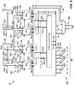
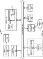
- FIG 2 is a schematic diagram of a baseband processor 20 that includes an exemplary vector processing unit 22, also referred to as a vector processing engine (VPE) 22.
- the baseband processor 20 and its VPE 22 can be provided in a semiconductor die 24.
- the baseband processor 20 includes a common VPE 22 that has programmable data path configurations.
- the VPE 22 includes common circuitry and hardware that can be programmed and reprogrammed to provide different, specific types of vector operations in different operation modes without the requirement to provide separate VPEs in the baseband processor 20.
- the VPE 22 can also be programmed in a vector arithmetic mode for performing general arithmetic operations in a highly efficient manner for multiple applications or technologies, without the requirement to provide separate VPEs in the baseband processor 20.
- the baseband processor 20 in this non-limiting example is a 512-bit vector processor.
- the baseband processor 20 includes additional components in addition to the VPE 22 to support the VPE 22 providing vector processing in the baseband processor 20.
- the baseband processor 20 includes vector registers 28 that are configured to receive and store vector data 30 from a vector unit data memory (LMEM) 32.
- LMEM vector unit data memory
- the vector data 30 is X bits wide, with 'X' defined according to design choice (e.g., 512 bits).
- the vector data 30 may be divided into vector data sample sets 34.
- the vector data 30 may be 256-bits wide and may comprise smaller vector data sample sets 34(Y)-34(0), where some of the vector data sample sets 34(Y)-34(0) are 16-bits wide, and others of the vector data sample sets 34(Y)-34(0) are 32-bits wide.
- the VPE 22 is capable of providing vector processing on certain chosen multiply vector data sample sets 34(Y)-34(0) provided in parallel to the VPE 22 to achieve a high degree of parallelism.
- the vector registers 28 are also configured to store results generated when the VPE 22 processes the vector data 30.
- the VPE 22 is configured to not store intermediate vector processing results in the vector registers 28 to reduce register writes to provide faster vector instruction execution times. This configuration is opposed to scalar instructions executed by scalar processing engines that store intermediate results in registers, such as scalar processing DSPs.
- the baseband processor 20 in Figure 2 also includes condition registers 36 configured to provide conditions to the VPE 22 for use in conditional execution of vector instructions and to store updated conditions as a result of vector instruction execution.
- the baseband processor 20 also includes accumulate registers 38, global registers 40, and address registers 42.
- the accumulate registers 38 are configured to be used by the VPE 22 to store accumulated results as a result of executing certain specialized operations on the vector data 30.
- the global registers 40 are configured to store scalar operands for certain vector instructions supported by the VPE 22.
- the address registers 42 are configured to store addresses addressable by vector load and store instructions supported by the VPE 22 to retrieve the vector data 30 from the vector unit data memory 32 and store vector processing results in the vector unit data memory 32.
- the baseband processor 20 in this aspect also includes a scalar processor 44 (also referred to as "integer unit”) to provide scalar processing in the baseband processor 20 in addition to vector processing provided by the VPE 22. It may be desired to provide a CPU configured to support both vector and scalar instruction operations based on the type of instruction executed for highly efficient operation.
- the scalar processor 44 is a 32-bit reduced instruction set computing (RISC) scalar processor as a non-limiting example.
- the scalar processor 44 includes an arithmetic logic unit (ALU) 46 for supporting scalar instruction processing in this example.
- ALU arithmetic logic unit
- the baseband processor 20 includes an instruction dispatch circuit 48 configured to fetch instructions from program memory 50, decode the fetched instructions, and direct the fetched instructions to either the scalar processor 44 or through the vector datapath 49 to the VPE 22 based on instruction type.
- the scalar processor 44 includes general purpose registers 52 for use by the scalar processor 44 when executing scalar instructions.
- An integer unit data memory (DMEM) 54 is included in the baseband processor 20 to provide data from main memory into the general purpose registers 52 for access by the scalar processor 44 for scalar instruction execution.
- the DMEM 54 may be cache memory as a non-limiting example.
- the baseband processor 20 also includes a memory controller 56 that includes memory controller registers 58 configured to receive memory addresses from the general purpose registers 52 when the scalar processor 44 is executing vector instructions requiring access to main memory through memory controller data paths 59.
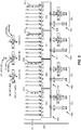
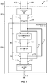
- Figure 3 illustrates an exemplary schematic diagram of the VPE 22 in Figure 2 .
- the VPE 22 includes a plurality of exemplary vector processing stages 60 having exemplary vector processing blocks that may be configured with programmable data path configurations.
- the programmable data path configurations provided in the vector processing blocks allow specific circuits and hardware to be programmed and reprogrammed to support performing different, specific vector processing operations on the vector data 30 received from the vector unit data memory 32 in Figure 2 .
- certain vector processing operations may commonly require multiplication of the vector data 30 followed by an accumulation of the multiplied vector data results.
- Non-limiting examples of such vector processing includes filtering operations, correlation operations, and Radix-2 and Radix-4 butterfly operations commonly used for performing Fast Fourier Transform (FFT) operations for wireless communications algorithms, where a series of parallel multiplications are provided followed by a series of parallel accumulations of the multiplication results.
- FFT Fast Fourier Transform
- the VPE 22 in Figure 2 fuses multipliers with carry-save accumulators to provide redundant carry-save format in the carry-save accumulators. Providing a redundant carry-save format in the carry-save accumulators can eliminate a need to provide a carry propagation path and a carry propagation add operation during each step of accumulation.
- the M0 multiply vector processing stage 60(1) is a second vector processing stage containing a plurality of vector processing blocks in the form of any desired number of multiplier blocks 62(A)-62(0), each having programmable data path configurations.
- the multiplier blocks 62(A)-62(0) are provided to perform vector multiply operations in the VPE 22.
- the plurality of multiplier blocks 62(A)-62(0) are disposed in parallel to each other in the M0 multiply vector processing stage 60(1) for providing multiplication of up to twelve (12) multiply vector data sample sets 34(Y)-34(0).
- 'A' is equal to three (3), meaning four (4) multiplier blocks 62(3)-62(0) are included in the M0 multiply vector processing stage 60(1) in this example.
- the multiply vector data sample sets 34(Y)-34(0) are loaded into the VPE 22 for vector processing into a plurality of latches 64(Y)-64(0) provided in an input read (RR) vector processing stage, which is a first vector processing stage 60(0) in the VPE 22.
- RR input read
- the latches 64(11)-64(0) are configured to latch the multiply vector data sample sets 34(11)-34(0) retrieved from the vector registers 28 (see Figure 2 ) as vector data input sample sets 66(11)-66(0).
- each latch 64(11)-64(0) is 8-bits wide.
- the latches 64(11)-64(0) are each respectively configured to latch the multiply vector data input sample sets 66(11)-66(0), for a total of 96-bits wide of vector data 30 (i.e., 12 latches x 8 bits each).
- the plurality of multiplier blocks 62(3)-62(0) are configured to be able to receive certain combinations of the vector data input sample sets 66(11)-66(0) for providing vector multiply operations, wherein 'Y' is equal to eleven (11) in this example.
- the multiply vector data input sample sets 66(11)-66(0) are provided in a plurality of input data paths A3-A0, B3-B0, and C3-C0 according to the design of the VPE 22.
- Vector data input sample sets 66(3)-66(0) correspond to input data paths C3-C0 as illustrated in Figure 3 .
- Vector data input sample sets 66(7)-66(4) correspond to input data paths B3-B0 as illustrated in Figure 3 .
- Vector data input sample sets 66(11)-66(8) correspond to input data paths A3-A0 as illustrated in Figure 3 .
- the plurality of multiplier blocks 62(3)-62(0) are configured to process the received vector data input sample sets 66(11)-66(0) according to the input data paths A3-A0, B3-B0, C3-C0, respectively, provided to the plurality of multiplier blocks 62(3)-62(0), to provide vector multiply operations.
- programmable internal data paths 67(3)-67(0) provided in the multiplier blocks 62(3)-62(0) in Figure 3 can be programmed to have different data path configurations. These different data path configurations provide different combinations and/or different bit lengths of multiplication of particular received vector data input sample sets 66(11)-66(0) provided to the multiplier blocks 62(3)-62(0) according to the particular input data paths A3-A0, B3-B0, C3-CO provided to each multiplier block 62(3)-62(0).
- the plurality of multiplier blocks 62(3)-62(0) provide vector multiply output sample sets 68(3)-68(0) as a vector result output sample set comprising a multiplication result of multiplying a particular combination of the vector data input sample sets 66(11)-66(0) together.
- the programmable internal data paths 67(3)-67(0) of the multiplier blocks 62(3)-62(0) may be programmed according to settings provided from a vector instruction decoder in the instruction dispatch 48 of the baseband processor 20 in Figure 2 .
- the vector instruction specifies the specific type of operation to be performed by the VPE 22.
- the VPE 22 can be programmed and reprogrammed to configure the programmable internal data paths 67(3)-67(0) of the multiplier blocks 62(3)-62(0) to provide different types of vector multiply operations with the same common circuitry in a highly efficient manner.
- the VPE 22 may be programmed to configure and reconfigure the programmable internal data paths 67(3)-67(0) of the multiplier blocks 62(3)-62(0) on a cycle-by-clock cycle basis for each vector instruction executed, according to decoding of the vector instructions in an instruction pipeline in the instruction dispatch 48.
- the M0 multiply vector processing stage 60(1) in the VPE 22 is configured to process vector data input sample sets 66 every clock cycle, as a result, the multiplier blocks 62(3)-62(0) perform vector multiply operations on every clock cycle according to decoding of the vector instructions in an instruction pipeline in the instruction dispatch 48.
- multiplier blocks 62 can be programmed to perform real and complex multiplications.
- a multiplier block 62 may be configured to multiply two 8-bit vector data input sample sets 66 together.
- a multiplier block 62 may be configured to multiply to two 16-bit vector data input sample sets 66 together, which are formed from a first pair of 8-bit vector data input sample sets 66 multiplied by a second pair of 8-bit vector data input sample sets 66. This is illustrated in Figure 6 and discussed in more detail below.
- multiplier blocks 62(3)-62(0) provides flexibility in that the multiplier blocks 62(3)-62(0) can be configured and reconfigured to perform different types of multiply operations to reduce area in the VPE 22 and possible allow fewer VPEs 22 to be provided in the baseband processor 20 to carry out the desired vector processing operations.
- the plurality of multiplier blocks 62(3)-62(0) are configured to provide the vector multiply output sample sets 68(3)-68(0) in programmable output data paths 70(3)-70(0) to either the next vector processing stage 60 or an output processing stage.
- the vector multiply output sample sets 68(3)-68(0) are provided in the programmable output data paths 70(3)-70(0) according to a programmed configuration based on the vector instruction being executed by the plurality of multiplier blocks 62(3)-62(0).
- the vector multiply output sample sets 68(3)-68(0) in the programmable output data paths 70(3)-70(0) are provided to the M1 accumulation vector processing stage 60(2) for accumulation, as will be discussed below.
- the vector multiply output sample sets 68(3)-68(0) are provided to a plurality of accumulator blocks 72(3)-72(0) provided in a next vector processing stage, which is the M1 accumulation vector processing stage 60(2).
- Each accumulator block among the plurality of accumulator blocks 72(A)-72(0) contains two accumulators 72(X)(1) and 72(X)(0) (i.e., 72(3)(1), 72(3)(0), 72(2)(1), 72(2)(0), 72(1)(1), 72(1)(0), and 72(0)(1), 72(0)(0)).
- the plurality of accumulator blocks 72(3)-72(0) accumulate the results of the vector multiply output sample sets 68(3)-68(0).
- the plurality of accumulator blocks 72(3)-72(0) are provided as carry-save accumulators, wherein the carry product is in essence saved and not propagated during the accumulation process until the accumulation operation is completed.
- the plurality of accumulator blocks 72(3)-72(0) are fused with the plurality of multiplier blocks 62(3)-62(0) in Figures 4 and 5 to provide redundant carry-save format in the plurality of accumulator blocks 72(3)-72(0).
- Providing redundant carry-save format in the plurality of accumulator blocks 72(3)-72(0) can eliminate a need to provide a carry propagation path and a carry propagation add operation during each step of accumulation in the plurality of accumulator blocks 72(3)-72(0).
- the M1 accumulation vector processing stage 60(2) and its plurality of accumulator blocks 72(3)-72(0) will now be introduced with reference to Figure 3 .
- the plurality of accumulator blocks 72(3)-72(0) in the M1 accumulation vector processing stage 60(2) are configured to accumulate the vector multiply output sample sets 68(3)-68(0) in programmable output data paths 74(3)-74(0) (i.e., 74(3)(1), 74(3)(0), 74(2)(1), 74(2)(0), 74(1)(1), 74(1)(0), and 74(0)(1), 74(0)(0)), according to programmable output data path configurations, to provide accumulator output sample sets 76(3)-76(0) (i.e., 76(3)(1), 76(3)(0), 76(2)(1), 76(2)(0), 76(1)(1), 76(1)(0), and 76(0)(1), 76(0)(0)) in either a next vector processing stage 60 or an output processing stage.
- 74(3)-74(0) i.e., 74(3)(1), 74(3)(0), 74(2)(1), 74(2)(0), 74(1)(1), 74(1)(0), and 74(0)(1), 76(0)(0)
- the accumulator output sample sets 76(3)-76(0) are provided to an output processing stage, which is an ALU processing stage 60(3).
- the accumulator output sample sets 76(3)-76(0) can also be provided to the ALU 46 in the scalar processor 44 in the baseband processor 20 in Figure 2 , as a non-limiting example.
- the ALU 46 may take the accumulator output sample sets 76(3)-76(0) according to the specialized vector instructions executed by the VPE 22 to be used in more general processing operations.
- programmable input data paths 78(3)-78(0) and/or programmable internal data paths 80(3)-80(0) of the accumulator blocks 72(3)-72(0) can be programmed to be reconfigured to receive different combinations and/or bit lengths of the vector multiply output sample sets 68(3)-68(0) provided from the multiplier blocks 62(3)-62(0) to the accumulator blocks 72(3)-72(0). Because each accumulator block 72 is comprised of two accumulators 72(X)(1), 72(X)(0), the programmable input data paths 78(A)-78(0) are shown in Figure 3 as 78(3)(1), 78(3)(0), 78(2)(1), 78(2)(0), 78(1)(1), 78(1)(0), and 78(0)(1), 78(0)(0).
- the programmable internal data paths 80(3)-80(A) are shown in Figure 3 as 80(3)(1), 80(3)(0), 80(2)(1), 80(2)(0), 80(1)(1), 80(1)(0), 80(0)(1), 80(0)(0).
- Providing programmable input data paths 78(3)-78(0) and/or programmable internal data paths 80(3)-80(0) in the accumulator blocks 72(3)-72(0) is discussed in more detail below with regard to Figures 8-9C .
- the accumulator blocks 72(3)-72(0) can provide the accumulator output sample sets 76(3)-76(0) according to the programmed combination of accumulated vector multiply output sample sets 68(3)-68(0).
- this provides flexibility in that the accumulator blocks 72(3)-72(0) can be configured and reconfigured to perform different types of accumulation operations based on the programming of the programmable input data paths 78(3)-78(0) and/or the programmable internal data paths 80(3)-80(0) to reduce area in the VPE 22 and possibly allow fewer VPEs 22 to be provided in the baseband processor 20 to carry out the desired vector processing operations.
- the programmable input data path 78 and/or the programmable internal data paths 80 of two accumulator blocks 72 may be programmed to provide for a single 40-bit accumulator as a non-limiting example. This is illustrated in Figure 9A and discussed in more detail below.
- the programmable input data path 78 and/or the programmable internal data path 80 of two accumulator blocks 72 may be programmed to provide for dual 24-bit accumulators as a non-limiting example. This is illustrated in Figure 9B and discussed in more detail below.
- the programmable input data path 78 and/or the programmable internal data path 80 of two accumulator blocks 72 may be programmed to provide for a 16-bit carry-save adder followed by a single 24-bit accumulator. This is illustrated in Figure 9C and discussed in more detail below. Specific, different combinations of multiplications and accumulation operations can also be supported by the VPE 22 according to the programming of the multiplier blocks 62(3)-62(0) and the accumulator blocks 72(3)-72(0) (e.g., 16-bit complex multiplication with 16-bit accumulation, and 32-bit complex multiplication with 16-bit accumulation).
- the programmable input data paths 78(3)-78(0) and/or the programmable internal data paths 80(3)-80(0) of the accumulator blocks 72(3)-72(0) may be programmed according to settings provided from a vector instruction decoder in the instruction dispatch 48 of the baseband processor 20 in Figure 2 .
- the vector instruction specifies the specific type of operation to be performed by the VPE 22.
- the VPE 22 can be configured to reprogram the programmable input data paths 78(3)-78(0) and/or the programmable internal data paths 80(3)-80(0) of the accumulator blocks 72(3)-72(0) for each vector instruction executed according to decoding of the vector instruction in an instruction pipeline in the instruction dispatch 48.
- a vector instruction may execute over one or more clock cycles of the VPE 22.
- the VPE 22 can be configured to reprogram the programmable input data paths 78(3)-78(0) and/or the programmable internal data paths 80(3)-80(0) of the accumulator blocks 72(3)-72(0) for each clock cycle of a vector instruction on a clock cycle-by-clock cycle basis.
- the programmable input data paths 78(3)-78(0) and/or the programmable internal data paths 80(3)-80(0) of the accumulator blocks 72(3)-72(0) can be reconfigured each clock cycle during execution of the vector instruction.
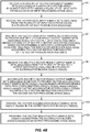
- Figures 4A and 4B are flowcharts illustrating exemplary vector processing of the multiplier blocks 62(A)-62(0) and the accumulator blocks 72(A)(1)-72(0)(0) in the VPE 22 in Figures 2 and 3 to provide more illustration of the exemplary vector processing.
- Figure 4A is a flowchart illustrating exemplary vector processing of a generalized vector processing block, which could be either the multiplier blocks 62(A)-62(0), the accumulator blocks 72(A)(1)-72(0)(0), or both, having programmable data path configurations included in the exemplary VPE of Figures 2 and 3 .
- Figure 4B is a flowchart illustrating exemplary vector processing of multiplier blocks 62(A)-62(0) and accumulator blocks 72(A)(1)-72(0)(0) each having programmable data path configurations and provided in different vector processing stages in the exemplary VPE 22 of Figures 2 and 3 .
- the process of the VPE 22 includes receiving a plurality of vector data input sample sets 34(Y)-34(0) of a width of a vector array in an input data path among a plurality of input data paths (A3-CO) in an input processing stage 60(0) (block 81).
- the vector processing next comprises receiving the vector data input sample sets 34(Y)-34(0) from the plurality of input data paths A3-CO in vector processing blocks 62(A)-62(0) and/or 72(A)(1)-72(0)(0) (block 83).
- the vector processing next includes processing the vector data input sample sets 34(Y)-34(0) to provide vector result output sample sets 68(A)-68(0), 76(A)(1)-76(0)(0) based on programmable data path configurations 67(A)-67(0), 70(3)-70(0), 78(A)(1)-78(0)(0), 80(A)(1)-80(0)(0), 74(A)(1)-74(0)(0) for vector processing blocks 62(A)-62(0), 72(A)(1)-72(0)(0) according to a vector instruction executed by the vector processing stage 60(1), 60(2) (block 85).
- the vector processing next includes providing the vector result output sample sets 68(A)-68(0), 76(A)(1)-76(0)(0) in output data paths 70(A)-70(0), 74(A)(1)-74(0)(0) (block 87).
- the vector processing next includes receiving the vector result output sample sets 68(A)-68(0), 76(A)(1)-76(0)(0) from the vector processing stage 60(1), 60(2) in an output processing stage 60(3) (block 89).
- each processing stage 60(0)-60(3) in the vector processing described above with regard to Figure 4A occurs concurrently for parallelization vector processing, wherein the programmable data path configurations 67(A)-67(0), 70(3)-70(0), 78(A)(1)-78(0)(0), 80(A)(1)-80(0)(0), 74(A)(1)-74(0)(0) of the vector processing blocks 62(A)-62(0), 72(A)(1)-72(0)(0) can be reprogrammed as often as each clock cycle. As discussed above, this allows the vector processing blocks 62(A)-62(0), 72(A)(1)-72(0)(0) to perform different operations for different vector instructions efficiently, and through the use of common vector processing blocks 62(A)-62(0), 72(A)(1)-72(0)(0).
- Figure 4B is a flowchart illustrating exemplary vector processing of the multiplier blocks 62(A)-62(0) and accumulator blocks 72(A)(1)-72(0)(0) in the VPE 22 in Figure 3 for vector instructions involving multiply operations followed by accumulate operations.
- FFT vector operations involve multiply operations followed by accumulate operations.
- the flowchart of Figure 4B provides further exemplary detail of the exemplary generalized vector processing of the VPE 22 described above in Figure 4A .
- the vector processing involves receiving a plurality of vector data input sample sets 34(Y)-34(0) of a width of a vector array in an input data path among a plurality of input data paths A3-C0 in an input processing stage 60(0) (block 93).
- the vector processing then includes receiving the vector data input sample sets 34(Y)-34(0) from the plurality of input data paths A3-C0 in a plurality of multiplier blocks 62(A)-62(0) (block 95).
- the vector processing then includes multiplying the vector data input sample sets 34(Y)-34(0) to provide multiply vector result output sample sets 68(A)-68(0) in multiply output data paths 70(A)-70(0) among a plurality of multiply output data paths 70(A)-70(0), based on programmable data path configurations 67(A)-67(0), 70(3)-70(0) for the multiplier blocks 62(A)-62(0) according to a vector instruction executed by the vector processing stage 60(1) (block 97).
- the vector processing next includes receiving the multiply vector result output sample sets 68(A)-68(0) from the plurality of multiply output data paths 70(A)-70(0) in a plurality of accumulator blocks 72(A)(1)-72(0)(0) (block 99).
- the vector processing next includes accumulating multiply vector result output sample sets 68(A)-68(0) together to provide vector accumulated result sample sets 76(A)(1)-76(0)(0) based on programmable data path 78(A)(1)-78(0)(0), 80(A)(1)-80(0)(0), 74(A)(1)-74(0)(0) configurations for the accumulator blocks 72(A)(1)-72(0)(0) according to a vector instruction executed by the second vector processing stage 60(2) (block 101).
- the vector processing then includes providing the vector accumulated result sample sets 76(A)(1)-76(0)(0) in the output data paths 74(A)(1)-74(0)(0) (block 103).
- the vector processing then includes receiving the vector result output sample sets 76(A)(1)-76(0)(0) from the accumulator blocks 72(A)(1)-72(0)(0) in an output processing stage 60(3) (block 105).
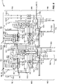
- Figure 5 is a more detailed schematic diagram of the plurality of multiplier blocks 62(3)-62(0) in the M0 multiply vector processing stage 60(1) of the VPE 22 of Figure 3 .
- Figure 6 is a schematic diagram of internal components of a multiplier block 62 in Figure 5 . As illustrated in Figure 5 , the vector data input sample sets 66(11)-66(0) that are received by the multiplier blocks 62(3)-62(0) according to the particular input data paths A3-A0, B3-B0, C3-C0 are shown. As will be discussed in more detail below with regard to Figure 6 , each of the multiplier blocks 62(3)-62(0) in this example include four (4) 8-bit by 8-bit multipliers.
- each of the multiplier blocks 62(3)-62(0) in this example are configured to multiply a multiplicand input 'A' by either multiplicand input 'B' or multiplicand input 'C.”
- the multiplicand inputs 'A,” and 'B' or 'C' that can be multiplied together in a multiplier block 62 are controlled by which input data paths A3-A0, B3-B0, C3-C0 are connected to the multiplier blocks 62(3)-62(0), as shown in Figure 5 .
- a multiplicand selector input 82(3)-82(0) is provided as an input to each multiplier block 62(3)-62(0) to control the programmable internal data paths 67(3)-67(0) in each multiplier block 62(3)-62(0) to select whether multiplicand input 'B' or multiplicand input 'C' is selected to be multiplied by multiplicand input 'A.'
- the multiplier blocks 62(3)-62(0) are provided with the capability for their programmable internal data paths 67(3)-67(0) to be reprogrammed to provide different multiply operations, as desired.
- input data paths A3 and A2 are connected to inputs AH and AL, respectively.
- Input AH represents the high bits of multiplicand input A
- AL means the low bits of input multiplicand input 'A.
- Input data paths B3 and B2 are connected to inputs BH and BL, respectively.
- Input BH represents the high bits of multiplicand input 'B
- AL represents the low bits of input multiplicand input 'B.”
- Input data paths C3 and C2 are connected to inputs CI and CQ, respectively.
- Input CI represents the real bits portion of input multiplicand input 'C' in this example.
- CQ represents the imaginary bits portion of input multiplicand input 'C' in this example.
- the multiplicand selector input 82(3) also controls whether the programmable internal data paths 67(3) of multiplier block 62(3) are configured to perform 8-bit multiplication on multiplicand input 'A' with multiplicand input 'B' or multiplicand input 'C,' or whether multiplier block 62(3) is configured to perform 16-bit multiplication on multiplicand input 'A' with multiplicand input 'B' or multiplicand input 'C' in this example.
- the multiplier blocks 62(3)-62(0) are configured to each generate vector multiply output sample sets 68(3)-68(0) as carry 'C' and sum 'S' vector output sample sets of the multiplication operation based on the configuration of their programmable internal data paths 67(3)-67(0).
- the carry 'C' and sum 'S' of the vector multiply output sample sets 68(3)-68(0) are fused, meaning that the carry 'C' and the sum 'S' are provided in redundant carry-save format to the plurality of accumulators 72(3)-72(0) to provide redundant carry-save format in the plurality of accumulators 72(3)-72(0).
- providing a redundant carry-save format in the plurality of accumulators 72(3)-72(0) can eliminate a need to provide a carry propagation path and a carry propagation add operation during accumulation operations performed by the plurality of accumulators 72(3)-72(0).
- multiplier blocks 62(3)-62(0) Examples of the multiplier blocks 62(3)-62(0) generating the vector multiply output sample sets 68(3)-68(0) as carry 'C' and sum 'S' vector output sample sets of the multiplication operation based on the configuration of their programmable internal data paths 67(3)-67(0) are shown in Figure 5 .
- multiplier block 62(3) is configured to generate carry C00 and sum S00 as 32-bit values for 8-bit multiplications and carry C01 and sum S01 as 64-bit values for 16-bit multiplications.
- the other multiplier blocks 62(2)-62(0) have the same capability in this example.
- multiplier block 62(2) is configured to generate carry C10 and sum S10 as 32-bit values for 8-bit multiplications and carry C11 and sum S11 as 64-bit values for 16-bit multiplications.
- Multiplier block 62(1) is configured to generate carry C20 and sum S20 as 32-bit values for 8-bit multiplications and carry C21, and sum S21 as 64-bit values for 16-bit multiplications.
- Multiplier block 62(0) is configured to generate carry C30 and sum S30 as 32-bit values for 8-bit multiplications and carry C31 and sum S31 as 64-bit values for 16-bit multiplications.
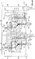
- Figure 6 is a schematic diagram of internal components of a multiplier block 62 in Figures 3 and 4 having programmable data path configurations capable of multiplying 8-bit by 8-bit vector data input sample set 66, and 16-bit by 16-bit vector data input sample set 66.
- the multiplier block 62 includes four 8x8-bit multipliers 84(3)-84(0) in this example. Any desired number of multipliers 84 could be provided.
- a first multiplier 84(3) is configured to receive 8-bit vector data input sample set 66A[H] (which is the high bits of input multiplicand input 'A') and multiply the vector data input sample set 66A[H] with either 8-bit vector data input sample set 66B[H] (which is the high bits of input multiplicand input 'B') or 8-bit vector data input sample set 66C[I] (which is the high bits of input multiplicand input 'C').
- a multiplexor 86(3) is provided that is configured to select either 8-bit vector data input sample set 66B[H] or 8-bit vector data input sample set 66C[I] being providing as a multiplicand to the multiplier 84(3).
- the multiplexor 86(3) is controlled by multiplicand selector bit input 82[3], which is the high bit in the multiplicand selector input 82 in this aspect.
- the multiplexor 86(3) and the multiplicand selector bit input 82[3] provide a programmable internal data path 67[0] configuration for the multiplier 84(3) to control whether 8-bit vector data input sample set 66B[H] or 8-bit vector data input sample set 66C[I] is multiplied with receive vector data input sample set 66A[H].
- multipliers 84(2)-84(0) also include similar programmable internal data paths 67[2]-67[0] as provided for the first multiplier 84(3).
- Multiplier 84(2) includes the programmable internal data path 67[2] having a programmable configuration to provide either 8-bit vector data input sample set 66B[H] or 8-bit vector data input sample set 66C[I] in the programmable internal data path 67[1] to be multiplied with 8-bit vector data input sample set 66A[L], which is the low bits of multiplicand input 'A.'
- the selection is controlled by multiplexor 86(2) according to the multiplicand selector bit input 82[2] in the multiplicand selector input 82 in this aspect.
- Multiplier 84(1) includes programmable internal data path 67[1] programmable to provide either 8-bit vector data input sample set 66B[L], which is the low bits of multiplicand input 'B,' or 8-bit vector data input sample set 66C[Q], which is the low bits of multiplicand input 'C' in the programmable internal data path 67[1] to be multiplied with 8-bit vector data input sample set 66A[H].
- the selection is controlled by multiplexor 86(1) according to the multiplicand selector bit input 82[1] in the multiplicand selector input 82 in this aspect.
- multiplier 84(0) includes programmable internal data path 67[0] programmable to provide either 8-bit vector data input sample set 66B[L] or 8-bit vector data input sample set 66C[Q] in the programmable internal data path 67[0], to be multiplied with 8-bit vector data input sample set 66A[L].
- the selection is controlled by multiplexor 86(0) according to the multiplicand selector bit input 82[0] in the multiplicand selector input 82 in this aspect.
- each multiplier 84(3)-84(0) can be configured to perform different bit length multiplication operations.
- each multiplier 84(3)-84(0) includes bit length multiply mode inputs 88(3)-88(0), respectively.
- each multiplier 84(3)-84(0) can be programmed in 8-bit by 8-bit mode according to the inputs that control the configuration of programmable data paths 90(3)-90(0), 91, and 92(3)-92(0), respectively.
- Each multiplier 84(3)-84(0) can also be programmed to provide part of a larger bit multiplication operation, including 16-bit by 16-bit mode and 24-bit by 8-bit mode, according to the inputs that control the configuration of programmable data paths 90(3)-90(0), 91, and 92(3)-92(0), respectively.
- the plurality of multipliers 84(3)-84(0) as a unit can be configured to comprise two (2) individual 8-bit by 8-bit multipliers as part of the multiplier block 62.
- each multiplier 84(3)-84(0) is configured in 16-bit by 16-bit multiply mode according to configuration of the programmable data path 91
- the plurality of multipliers 84(3)-84(0) as a unit can be configured to comprise a single 16-bit by 16-bit multiplier as part of the multiplier block 62.
- the multipliers 84(3)-84(0) are configured in 24-bit by 8-bit multiply mode according to configuration of the programmable data paths 92(3)-92(0)
- the plurality of multipliers 84(3)-84(0) as a unit can be configured to comprise one (1) 16-bit by 24-bit by 8-bit multiplier as part of the multiplier block 62.
- the multipliers 84(3)-84(0) in this example are shown as being configured in 16-bit by 16-bit multiply mode. Sixteen (16)-bit input sums 94(3), 94(2) and input carries 96(3), 96(2) are generated by each multiplier 84(3), 84(2), respectively. Sixteen (16)-bit input sums 94(1), 94(0) and input carries 96(1), 96(0) are generated by each multiplier 84(1), 84(0), respectively.
- the 16-bit input sums 94(3), 94(2) and input carries 96(3), 96(2) are also provided to a 24-bit 4:2 compressor 109 along with 16-bit sums input 94(1), 94(0) and input carries 96(1), 96(0) to add the input sums 94(3)-94(0) and input carries 96(3)-96(0) together.
- the added input sums 94(3)-94(0) and input carries 96(3)-96(0) provide a single sum 98 and single carry 100 in 16-bit by 16-bit multiply mode when the programmable data path 91 is active and gated with the input sums 94(3)-94(0) and input carries 96(3)-96(0).
- the programmable data path 91 is gated by a first AND-based gate 102(3) with combined input sums 94(3), 94(2) as a 16-bit word, and by a second AND-based gate 102(2) with combined input carries 96(3), 96(2) as a 16-bit word to be provided to the 24-bit 4:2 compressor 109.
- the programmable data path 91 is also gated by a third AND-based gate 102(1) with combined input sums 94(1), 94(0) as a 16-bit word, and by a fourth AND-based gate 102(0) with combined input carries 96(1), 96(0) as a 16-bit word to be provided to the 24-bit 4:2 compressor 109.
- the programmable output data path 70[0] is provided with the vector multiply output sample set 68[0] as a compressed 32-bit sum S0 and 32-bit carry C0 partial product if the multiplier block 62 is configured in a 16-bit by 16-bit or 24-bit by 8-bit multiply mode.
- the programmable output data path 70[1] configuration is provided as the 16-bit input sums 94(3)-94(0) and corresponding 16-bit input carries 96(3)-96(0) as partial products without compression, if the multipliers 84(3)-84(0) in the multiplier block 62 are configured in 8-bit by 8-bit multiply mode.
- the programmable output data path 70[1] is provided as the 16-bit input sums 94(3)-94(0) and corresponding 16-bit input carries 96(3)-96(0) as the vector multiply output sample sets 68[1] without compression if the multipliers 84(3)-84(0) in the multiplier block 62 are configured in 8-bit by 8-bit multiply mode.
- the vector multiply output sample sets 68[0], 68[1], depending on a multiplication mode of the multiplier block 62, are provided to the accumulator blocks 72(3)-72(0) for accumulation of sum and carry products according to the vector instruction being executed.
- multiplier blocks 62(3)-62(0) in Figures 4 and 5 having programmable data path configurations have been described, features of the multiplier blocks 62(3)-62(0) in the VPE 22 fused with the accumulator blocks 72(3)-72(0) configured in redundant carry-save format will now described in general with regard to Figure 7 .
- Figure 7 is a generalized schematic diagram of a multiplier block and accumulator block in the VPE of Figures 2 and 3 , wherein the accumulator block employs a carry-save accumulator structure employing redundant carry-save format to reduce carry propagation.
- the multiplier blocks 62 are configured to multiply multiplicand inputs 66[H] and 66[L] and provide at least one input sum 94 and at least one input carry 96 as a vector multiply output sample sets 68 in the programmable output data path 70.
- the at least one input sum 94 and the at least one input carry 96 in the vector multiply output sample sets 68 in the programmable output data path 70 are fused in redundant carry-save format to at least one accumulator block 72.
- the carry 96 in the vector multiply output sample sets 68 is provided as vector input carry 96 in carry-save format to the accumulator block 72.
- the input sum 94 and the input carry 96 in the vector multiply output sample sets 68 can be provided to a compressor 108 of the accumulator block 72, which in this aspect is a complex gate 4:2 compressor.
- the compressor 108 is configured to accumulate the input sum 94 and the input carry 96 together with a previous accumulated vector output sum 112 and a previous shifted accumulated vector output carry 117, respectively.
- the previous shifted accumulated vector output carry 117 is in essence the saved carry accumulation during the accumulation operation.
- the compressor 108 is configured to accumulate the input sum 94 and the input carry 96 in a redundant form with the previous accumulated vector output sum 112 and previous shifted accumulated vector output carry 117, respectively.
- the shifted accumulated vector output carry 117 is generated by an accumulated vector output carry 114 generated by the compressor 108 bit by shifting the accumulated vector output carry 114 before the next accumulation of the next received input sum 94 and input carry 96 is performed by the compressor 108.
- the final shifted accumulated vector output carry 117 is added to the final accumulated vector output sum 112 by a single, final carry propagate adder 119 provided in the accumulator block 72 propagate the carry accumulation in the final shifted accumulated vector output carry 117 to convert the final accumulated vector output sum 112 to the final accumulator output sample set 76 2's complement notation.
- the final accumulated vector output sum 112 is provided as accumulator output sample set 76 in the programmable output data path 74 (see Figure 3 ).
- FIG. 7 illustrating the fusing of a multiplier blocks 62 with an accumulator block 72 configured in redundant carry-save format
- FIG. 8 more exemplary detail regarding the accumulator blocks 72(3)-72(0) are now described in general with regard to Figure 8 .
- Figures 9A-9C described below provide more exemplary detail of the accumulator blocks 72(3)-72(0) configured in redundant carry-save format in different accumulation modes to provide different vector accumulation operations with common circuitry and hardware.
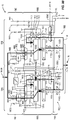
- Figure 8 is a detailed schematic diagram of exemplary internal components of an accumulator block 72 provided in the VPE 22 of Figure 3 .
- the accumulator block 72 is configured with programmable input data paths 78(3)-78(0) and/or the programmable internal data paths 80(3)-80(0), so that the accumulator block 72 can be programmed to act as dedicated circuitry designed to perform specific, different types of vector accumulation operations.
- the accumulator block 72 can be programmed to provide a number of different accumulations and additions, including signed and unsigned accumulate operations.
- the accumulator block 72 is configured to include carry-save accumulators 72[0], 72[1] to provide redundant carry arithmetic to avoid or reduce carry propagation to provide high speed accumulation operations with reduced combinational logic.
- Exemplary internal components of the accumulator block 72 are shown in Figure 8 .
- the accumulator block 72 in this aspect is configured to receive a first input sum 94[0] and first input carry 96[0], and a second input sum 94[1] and second input carry 96[1] from a multiplier block 62 to be accumulated together.
- the input sums 94[0], 94[1] and input carries 96[0], 96[1] will be referred to as vector input sums 94[0], 94[1] and vector input carries 96[0], 96[1].
- the vector input sums 94[0], 94[1] and vector input carries 96[0], 96[1] in this aspect are each 16-bits in length.
- the accumulator block 72 in this example is provided as two 24-bit carry-save accumulators 72[0], 72[1], each containing similar components with common element numbers with '[0]' being designated for carry-save accumulator 72[0], and with '[1]' being designated for carry-save accumulator 72[1].
- the carry-save accumulators 72[0], 72[1] can be configured to perform vector accumulation operations concurrently.
- the vector input sum 94[0] and vector input carry 96[0] are input in a multiplexor 104(0) provided as part of the programmable internal data path 80[0].
- a negation circuit 106(0) which may be comprised of exclusive OR-based gates, is also provided that generates a negative vector input sum 94[0]' and negative vector input carry 96[0]' according to an input 107(0), as inputs into the multiplexor 104(0) for accumulation operations requiring a negative vector input sum 94[0]' and negative vector input carry 96[0]'.
- the multiplexor 104(0) is configured to select either vector input sum 94[0] and vector input carry 96[0] or the negative vector input sum 94[0]' and the negative vector input carry 96[0]' to be provided to a compressor 108(0) according to a selector input 110(0) generated as a result of the vector instruction decoding.
- the selector input 110(0) allows the programmable input data path 78[0] of carry-save accumulator 72[0] to be programmable to provide either the vector input sum 94[0] and vector input carry 96[0], or the negative vector input sum 94[0]' and the negative vector input carry 96[0]', to the compressor 108(0) according to the accumulation operation configured to be performed by the accumulator block 72.
- the compressor 108(0) of the carry-save accumulator 72[0] in this aspect is a complex gate 4:2 compressor.
- the compressor 108(0) is configured to accumulate sums and carries in redundant carry-save operations.
- the compressor 108(0) is configured to accumulate a current vector input sum 94[0] and vector input carry 96[0], or a current negative vector input sum 94[0]' and negative vector input carry 96[0]', together with previous accumulated vector input sum 94[0] and vector input carry 96[0], or accumulated negative vector input sum 94[0]' and negative vector input carry 96[0]', as the four (4) inputs to the compressor 108(0).
- the compressor 108(0) provides an accumulated vector output sum 112(0) and accumulated vector output carry 114(0) as the accumulator output sample set 76[0] in the programmable output data path 74[0] (see Figure 3 ) to provide accumulator output sample sets 76(3)-76(0).
- the accumulated vector output carry 114(0) is shifted by a bit shifter 116(0) during accumulation operations to provide a shifted accumulated vector output carry 117(0) to control bit width growth during each accumulation step.
- the bit shifter 116(0) in this aspect is a barrel-shifter that is fused to the compressor 108(0) in redundant carry-save format.
- the shifted accumulated vector output carry 117(0) is in essence saved without having to be propagated to the accumulated vector output sum 112(0) during the accumulation operation performed by the accumulator 72[0].
- power consumption and gate delay associated with performing a carry propagation add operation during each step of accumulation in the accumulator 72[0] is eliminated in this aspect.
- Additional follow-on vector input sums 94[0] and vector input carries 96[0], or negative vector input sums 94[0]' and negative vector input carries 96[0]', can be accumulated with the current accumulated vector output sum 112(0) and current accumulated vector output carry 117(0).
- the vector input sums 94[0] and vector input carries 96[0], or negative vector input sums 94[0]' and negative vector input carries 96[0]', are selected by a multiplexor 118(0) as part of the programmable internal data path 80[0] according to a sum-carry selector 120(0) generated as a result of the vector instruction decoding.
- the current accumulated vector output sum 112(0) and current shifted accumulated vector output carry 117(0) can be provided as inputs to the compressor 108(0) for carry-save accumulator 72[0] to provide an updated accumulated vector output sum 112(0) and accumulated vector output carry 114(0).
- the sum-carry selector 120(0) allows the programmable internal data path 80[0] of accumulator 72[0] to be programmable to provide the vector input sum 94[0] and vector input carry 96[0] to the compressor 108(0) according to the accumulation operation configured to be performed by the accumulator block 72.
- Hold gates 122(0), 124(0) are also provided in this aspect to cause the multiplexor 118(0) to hold the current state of the accumulated vector output sum 112(0) and shifted accumulated vector output carry 117(0) according to a hold state input 126(0) to control operational timing of the accumulation in the carry-save accumulator 72[0].
- the control gates 134(0), 136(0) and 134(1), 136(1) control the accumulated vector output sum 112(0) and shifted accumulated vector output carry 117(0), and the accumulated vector output sum 112(1) and shifted accumulated vector output carry 117(1), respectively, being returned to the compressors 108(0), 108(1).
- the accumulator block 72 can be configured in different modes.
- the accumulator block 72 can be configured to provide different accumulation operations according to a specific vector processing instruction with common accumulator circuitry illustrated in Figure 8 . Examples of the accumulator block 72 being configured to provide different accumulation operations according to a specific vector processing instruction with common accumulator circuitry are illustrated in Figures 9A-9C below.
- Figure 9A is a schematic diagram of the same accumulator block 72 in Figure 8 .
- the accumulator block 72 has programmable input data paths 78[0], 78[1] and programmable internal data paths 80[0], 80[1] programmed to provide a dual 24-bit accumulator mode.
- Each carry-save accumulator 72[0], 72[1] in the accumulator block 72 in Figure 9A is configured to provide a 24-bit accumulator.
- the 24-bit accumulation capacities of the accumulators 72[0], 72[1] are provided by the bit capacity of the compressors 108(0), 108(1).
- carry-save accumulator 72[0] With continuing reference to Figure 9A , the exemplary components of carry-save accumulator 72[0] will be described, but are equally applicable to carry-save accumulator 72[1].
- the accumulated vector output sum 112(0) and shifted accumulated vector output carry 117(0) of carry-save accumulator 72[0] and the accumulated vector output sum 112(1) and shifted accumulated vector output carry 117(1) of carry-save accumulator 72[1] are gated by the control gates 134(0), 136(0) and 134(1), 136(1), respectively.
- control gates 134(0), 136(0) and 134(1), 136(1) control the accumulated vector output sum 112(0) and shifted accumulated vector output carry 117(0), and the accumulated vector output sum 112(1) and shifted accumulated vector output carry 117(1), respectively, being returned to the compressors 108(0), 108(1).
- Control inputs 138(0), 138(1) provided from decoding of vector instructions to both control gates 134(0), 136(0) and 134(1), 136(1), respectively, control the accumulated vector output sum 112(0) and shifted accumulated vector output carry 117(0), and the accumulated vector output sum 112(1) and shifted accumulated vector output carry 117(1), respectively, are returned to the compressors 108(0), 108(1).
- control inputs 138(0), 138(1) and control gates 134(0), 136(0) control whether the accumulators 72[0], 72[1] are programmed to each perform separate accumulation operations or combined accumulation operations, as will be discussed in more detail below with regard to Figures 9B and 9C .
- the control inputs 138(0), 138(1) and the control gates 134(0), 136(0) and 134(1), 136(1) form part of the programmable internal data paths 80[0], 80[1] of the accumulators 72[0], 72[1], respectively, in this aspect.
- the programmable internal data paths 80[0], 80[1] of the accumulator block 72 can also be programmed and/or reprogrammed to perform accumulate operations greater than the 24-bit capacity of the individual accumulators 72[0], 72[1].
- the programmable internal data paths 80[0], 80[1] of the accumulators 72[0], 72[1] can be programmed to provide for both accumulators 72[0], 72[1] to be employed together in a single vector accumulation operation.
- the accumulators 72[0], 72[1] can be programmed to provide a single accumulation operation of greater bit capacity than the individual bit accumulation capacities of the accumulators 72[0], 72[1].
- the programmable internal data paths 80[0], 80[1] of the accumulators 72[0], 72[1] can be configured to allow carry-save accumulator 72[0] to propagate an overflow carry output as a next carry output (NCO) 137(0) from compressor 108(0).
- the NCO 137(0) can be provided as a next carry input (NCI) 139(1) to compressor 108(1) in carry-save accumulator 72[1].
- This carry propagation configuration capability provided as programmable internal data paths 80[0], 80[1] in the accumulators 72[0], 72[1] to allow the accumulators 72[0], 72[0] to provide 24-bit overflow carry propagation to 24-bit carry and sum accumulations, as previously described with regard to Figure 8 , to provide 40-bit accumulation in this aspect.
- Figure 9B is a schematic diagram of the same accumulator block 72 in Figure 8 .
- the accumulator block 72 is shown configured in a single accumulation operation mode.
- the accumulators 72[0], 72[1] have programmable internal data paths 80[0], 80[1] configured for providing a single accumulation operation in the accumulator block 72.
- the accumulators 72[0], 72[1] accumulate a single 40-bit accumulated vector output sum 112 and shifted accumulated vector output carry 117.
- the single accumulated vector output sum 112 is comprised of the accumulated vector output sums 112(0), 112(1) provided as an accumulator output sample set 76 in programmable output data paths 74[0], 74[1] (see also, Figure 3 ).
- the accumulated vector output sum 112(0) comprises the least significant bits of the single 40-bit accumulated vector output sum 112.
- the accumulated vector output sum 112(1) comprises the most significant bits of the single 40-bit accumulated vector output sum 112.
- the shifted accumulated vector output carry 117 is comprised of the shifted accumulated output carries 117(0), 117(1).
- the shifted accumulated vector output carry 117(0) comprises the least significant bits of the single shifted accumulated vector output carry 117.
- the accumulated vector output sum 114(1) comprises the most significant bits of the single 40-bit accumulated vector output carry 114.
- the accumulate vector output sum 114[0] and shifted accumulated vector output carry 117(0) are provided in programmable output data path 74[0] (see Figure 3 ).
- the general data path of accumulation operations performed by accumulators 72[0], 72[1] when the accumulator block 72 is configured in a single accumulation mode is shown as programmable accumulate data path 146.
- the accumulator block 72 receives the vector input sum 94 and vector input carry 96 as previously described.
- the carry-save accumulator 72[0] accumulates the least significant bits of accumulated vector output sum 112(0) and accumulated vector output carry 114(0) from accumulations of the vector input sums 94[0] and vector input carries 96[0], or negative vector input sums 94[0]' and negative vector input carries 96[0]'s, as the case may be.
- the carry-save accumulator 72[1] accumulates the most significant bits of the accumulated vector output sum 112(1) and accumulated vector output carry 114(1) from accumulations of the vector input sums 94[0] and vector input carries 96[0], or negative vector input sums 94[0]' and negative vector input carries 96[0]'s, as the case may be.
- the programmable internal data paths 80[0],80[1] of accumulators 72[0], 72[1] are programmed to provide a single accumulation operation.
- the NCO 137(0) of compressor 108(0) of carry-save accumulator 72[0] and the NCI 139(1) of compressor 108(1) of carry-save accumulator 72[1] are configured for providing a single accumulator (e.g., 40-bit accumulator) in the accumulator block 72.
- the NCI 139(1) of the carry-save accumulator 72[1] is gated by NCI gate 140(1) with NCI control input 142(1).
- NCI control input 142(1) can be made active as part of the programmable internal data path 80[1] of the carry-save accumulator 72[1].
- the NCI control input 142(1) causes the NCI gate 140(1) to allow an overflow carry propagation from the compressor 108(0) to compressor 108(1).
- the NCI control input 142(1) is also coupled to a carry propagate input 144(0) of the compressor 108(0) in carry-save accumulator 72[0] to cause the compressor 108(0) to generate the NCO 137(0) as NCI 139(1) to compressor 108(1).
- These configurations allow the carry-save accumulator 72[1] to accumulate vector input sums 94[1] and vector input carries 96[1] in a manner that can provide a single accumulated vector output sum 112 and accumulated vector output carry 114.
- carry-save accumulator 72[1] in the accumulator block 72 also includes a NCI gate 140(0) gated by NCI 139(0) and NCI control input 142(0), as shown in Figure 9B .
- both NCI control input 142(0) and NCI 139(0) are tied to logical '0' in this aspect since carry-save accumulator 72[0] accumulates the least significant bits of the single accumulation operation.
- compressor 108(0) of carry-save accumulator 72[1] also includes a carry propagate input 144(1), but the carry propagate input 144(1) is tied to logical '0' in this aspect to cause the accumulator 72(1) to not generate the NCO 12(1).
- the carry-save accumulator 72[1] does not need to perform carry propagation to a next accumulator in this aspect, since there is not another accumulator beyond carry-save accumulator 72[1] provided in this aspect of the accumulator block 72.
- Figure 9C is a schematic diagram of another accumulator mode of the same accumulator block 72 in Figure 8 .
- Figure 9C is a schematic diagram of the accumulator block 72 in Figure 8 having programmed data path configurations to provide a carry-save adder followed by a single accumulator to provide another accumulation mode in the accumulator block 72. Some accumulation operations may require an extra adder to perform complex arithmetic.
- the accumulators 72[0], 72[1] have programmable internal data paths 80[0], 80[1] configured for providing a 16-bit carry-save adder followed by a single 24-bit accumulator.
- the general data path of accumulations performed by accumulators 72[0], 72[1] when the accumulator block 72 is configured in carry-save adder followed by a single accumulator is shown by programmable data path 148.
- the sum-carry selector 120(0) is generated as a result of the vector instruction decoding to cause the multiplexor 118(0) to provide the vector input sum 94[1] and vector input carry 96[0] to the control gates 134(0), 136(0).
- the control input 138(0) is made active to program the programmable internal data path 80[1] of carry-save accumulator 72[0] to cause the control gates 134(0), 136(0) to provide the vector input sum 94[1] and vector input carry 96[1] to the compressor 108(0).
- the vector input sum 94[1] and vector input carry 96[1] are accumulated with the vector input sum 94[0] and vector input carry 96[1] by the compressor 108(0) of the carry-save accumulator 72[0] to provide the accumulated vector output sum 112(0) and accumulated vector output carry 114(0).
- the accumulated vector output sum 112(0) and shifted accumulated vector output carry 117(0) are provided as the accumulator output sample set 76[0] in programmable output data path 74[0] (see also, Figure 3 ) to provide a carry-save adder.
- the shifted accumulated vector output carry 117(0) is also provided to carry-save accumulator 72[1] as shown in programmable data path 148 to be provided by multiplexor 104(1) to compressor 108(1) to be accumulated to vector input sum 94[1] and vector input carry 96[1] to provide accumulated vector output sum 112(1) and shifted accumulated vector output carry 117(1) as accumulator output sample set 76[1] in programmable output data path 74[1] (see also, Figure 3 ) as a 24-bit accumulator.
- VPEs having programmable data path configurations for vector processing may be provided in or integrated into any processor-based device.
- Examples include a set top box, an entertainment unit, a navigation device, a communications device, a fixed location data unit, a mobile location data unit, a mobile phone, a cellular phone, a computer, a portable computer, a desktop computer, a personal digital assistant (PDA), a monitor, a computer monitor, a television, a tuner, a radio, a satellite radio, a music player, a digital music player, a portable music player, a digital video player, a video player, a digital video disc (DVD) player, and a portable digital video player.
- PDA personal digital assistant
- Figure 10 illustrates an example of a processor-based system 150.
- the processor-based system 150 includes one or more processing units (PUs) 152, each including one or more processors or cores 154.
- the PU 152 may be the baseband processor 20 in Figure 2 as a non-limiting example.
- the processor 154 may be a vector processor like the baseband processor 20 provided in Figure 2 as a non-limiting example.
- the processor 154 may also include a VPE 156, including but not limited to the VPE 22 in Figure 2 .
- the PU(s) 152 may have cache memory 158 coupled to the processor(s) 154 for rapid access to temporarily stored data.
- the PU(s) 152 is coupled to a system bus 160 and can intercouple master and slave devices included in the processor-based system 150. As is well known, the PU(s) 152 communicates with these other devices by exchanging address, control, and data information over the system bus 160. For example, the PU(s) 152 can communicate bus transaction requests to a memory controller 162 as an example of a slave device. Although not illustrated in Figure 10 , multiple system buses 160 could be provided, wherein each system bus 160 constitutes a different fabric.
- Other master and slave devices can be connected to the system bus 160. As illustrated in Figure 10 , these devices can include a memory system 164, one or more input devices 166, one or more output devices 168, one or more network interface devices 170, and one or more display controllers 172, as examples.
- the memory system 164 can include memory 165 accessible by the memory controller 162.
- the input device(s) 166 can include any type of input device, including but not limited to input keys, switches, voice processors, etc.
- the output device(s) 168 can include any type of output device, including but not limited to audio, video, other visual indicators, etc.
- the network interface device(s) 170 can be any devices configured to allow exchange of data to and from a network 174.
- the network 174 can be any type of network, including but not limited to a wired or wireless network, a private or public network, a local area network (LAN), a wide local area network (WLAN), and the Internet.
- the network interface device(s) 170 can be configured to support any type of communication protocol desired.
- the CPUs 152 may also be configured to access the display controller(s) 172 over the system bus 160 to control information sent to one or more displays 178.
- the display controller(s) 172 sends information to the display(s) 178 to be displayed via one or more video processors 180, which process the information to be displayed into a format suitable for the display(s) 178.
- the display(s) 178 can include any type of display, including but not limited to a cathode ray tube (CRT), a liquid crystal display (LCD), a plasma display, etc.
- a processor may be a microprocessor, but in the alternative, the processor may be any conventional processor, controller, microcontroller, or state machine.
- a processor may also be implemented as a combination of computing devices, e.g., a combination of a DSP and a microprocessor, a plurality of microprocessors, one or more microprocessors in conjunction with a DSP core, or any other such configuration.
- RAM Random Access Memory
- ROM Read Only Memory
- EPROM Electrically Programmable ROM
- EEPROM Electrically Erasable Programmable ROM
- registers hard disk, a removable disk, a CD-ROM, or any other form of computer readable medium known in the art.
- An exemplary storage medium is coupled to the processor such that the processor can read information from, and write information to, the storage medium.
- the storage medium may be integral to the processor.
- the processor and the storage medium may reside in an ASIC.
- the ASIC may reside in a remote station.
- the processor and the storage medium may reside as discrete components in a remote station, base station, or server.
Description
- The present application is related to
U.S. Patent Application Serial No. 13/798,599 - The present application is also related to
U.S. Patent Application Serial No. 13/798,618 - The field of the disclosure relates to vector processors and related systems for processing vector and scalar operations, including single instruction, multiple data (SIMD) processors and multiple instruction, multiple data (MIMD) processors.
- Wireless computing systems are fast becoming one of the most prevalent technologies in the digital information arena. Advances in technology have resulted in smaller and more powerful wireless communications devices. For example, wireless computing devices commonly include portable wireless telephones, personal digital assistants (PDAs), and paging devices that are small, lightweight, and easily carried by users. More specifically, portable wireless telephones, such as cellular telephones and Internet Protocol (IP) telephones, can communicate voice and data packets over wireless networks. Further, many such wireless communications devices include other types of devices. For example, a wireless telephone may include a digital still camera, a digital video camera, a digital recorder, and/or an audio file player. Also, wireless telephones can include a web interface that can be used to access the Internet. Further, wireless communications devices may include complex processing resources for processing high speed wireless communications data according to designed wireless communications technology standards (e.g., code division multiple access (CDMA), wideband CDMA (WCDMA), and long term evolution (LTE)). As such, these wireless communications devices include significant computing capabilities.
- As wireless computing devices become smaller and more powerful, they become increasingly resource constrained. For example, screen size, amount of available memory and file system space, and amount of input and output capabilities may be limited by the small size of the device. Further, battery size, amount of power provided by the battery, and life of the battery are also limited. One way to increase the battery life of the device is to design processors that consume less power.
- In this regard, baseband processors may be employed for wireless communications devices that include vector processors. Vector processors have a vector architecture that provides high-level operations that work on vectors, i.e. arrays of data. Vector processing involves fetching a vector instruction once and then executing the vector instruction multiple times across an entire array of data elements, as opposed to executing the vector instruction on one set of data and then re-fetching and decoding the vector instruction for subsequent elements within the vector. This process allows the energy required to execute a program to be reduced, because among other factors, each vector instruction needs to be fetched fewer times. Since vector instructions operate on long vectors over multiple clock cycles at the same time, a high degree of parallelism is achievable with simple in-order vector instruction dispatch.
-
Figure 1 illustrates anexemplary baseband processor 10 that may be employed in a computing device, such as a wireless computer device. Thebaseband processor 10 includes multiple processing engines (PEs) 12 each dedicated to providing function-specific vector processing for specific applications. In this example, six (6) separate PEs 12(0)-12(5) are provided in thebaseband processor 10. The PEs 12(0)-12(5) are each configured to provide vector processing for fixed X-bitwide vector data 14 provided from a sharedmemory 16 to the PEs 12(0)-12(5). For example, thevector data 14 could be 512 bits wide. Thevector data 14 can be defined in smaller multiples of X-bit width vector data sample sets 18(0)-18(Y) (e.g., 16-bit and 32-bit sample sets). In this manner, the PEs 12(0)-12(5) are capable of providing vector processing on multiple vector data sample sets provided in parallel to the PEs 12(0)-12(5) to achieve a high degree of parallelism. Each PE 12(0)-12(5) may include a vector register file (VR) for storing the results of a vector instruction processed on thevector data 14. - Each PE 12(0)-12(5) in the
baseband processor 10 inFigure 1 includes specific, dedicated circuitry and hardware specifically designed to efficiently perform specific types of fixed operations. For example, thebaseband processor 10 inFigure 1 includes separate Wideband Code Division Multiple Access (WCDMA) PEs 12(0), 12(1) and Long Term Evolution (LTE) PEs 12(4), 12(5), because WCDMA and LTE involve different types of specialized operations. Thus, by providing separate WCDMA-specific PEs 12(0), 12(1) and LTE-specific PEs 12(4), 12(5), each of the PEs 12(0), 12(1), 12(4), 12(5) can be designed to include specialized, dedicated circuitry that is specific to frequently performed functions for WCDMA and LTE for highly efficient operation. This design is in contrast to scalar processing engines that include more general circuitry and hardware designed to be flexible to support a larger number of unrelated operations, but in a less efficient manner. - Providing function-specific PEs in a baseband processor is advantageous for frequently executed, specialized operations. However, providing function-specific PEs can increase area and power needed for the baseband processor, because the separate function-specific PEs each include specialized circuitry and memories. Further reference is made to
US 2004003206 (A1) "STREAMING VECTOR PROCESSOR WITH RECONFIGURABLE INTERCONNECTION SWITCH" disclosing a re-configurable streaming vector processor which includes a number of function units, each having one or more inputs for receiving data values and an output for providing a data value, a re-configurable interconnection switch and a micro-sequencer. The re-configurable interconnection switch includes one or more links, each link operable to couple an output of a function unit to an input of a function unit as directed by the micro-sequencer. The vector processor may also include one or more input-stream units for retrieving data from memory. Each input-stream unit is directed by a host processor and has a defined interface to the host processor. The vector processor also includes one or more output-stream units for writing data to memory or to the host processor. The defined interface of the input-stream and output-stream units forms a first part of the programming model. The instructions stored in a memory, in the sequence that direct the re-configurable interconnection switch, form a second part of the programming model. - The present invention is set forth in the independent claims, respectively. Preferred embodiments of the invention are described in the dependent claims.
- Aspects useful for the understanding of the invention disclosed herein include vector processing engines (VPEs) having programmable data path configurations for providing multi-mode vector processing. Related vector processors, systems, and methods are also disclosed. The VPEs disclosed herein include at least one vector processing stage configured to process vector data according to a vector instruction being executed by a vector processing stage. Each vector processing stage includes one or more vector processing blocks configured to process vector data based on the vector instruction being executed. Vector processing blocks are multipliers and accumulators. The vector processing blocks are capable of providing different functions for different types of instructions in different modes based on a programmable data path configuration of the vector processing blocks. In this manner, a VPE can be provided with its data path configurations reprogrammable to execute different types of functions according to the vector instruction being executed.
- As a result, fewer VPEs can provide desired technology specific, thus saving area in the baseband processor while still retaining vector processing advantages of fewer register writes and faster instruction execution compared to scalar processing engines. The data path configurations for the vector processing blocks may also be programmed and reprogrammed during vector instruction execution in the VPE to support execution of different, specialized vector operations in different modes in the VPE.
- The VPEs having programmable data path configurations for multi-mode vector processing disclosed herein are distinguishable from VPEs that only include fixed data path configurations to provide fixed functions. The VPEs having programmable data path configurations for vector processing disclosed herein are also distinguishable from scalar processing engines, such as those provided in digital signal processors (DSPs) for example. Scalar processing engines employ flexible, common circuitry and logic to perform different types of non-fixed functions, but also write intermediate results during vector instruction execution to register files, thereby consuming additional power and increasing vector instruction execution times.
- In this regard in one aspect, a VPE is provided. The VPE is configured to provide multi-mode vector processing of vector data. The VPE comprises an input read stage configured to provide a plurality of vector data input sample sets of a width of a vector array in an input data path among a plurality of input data paths. The VPE also comprises at least one vector processing stage comprising a plurality of vector processing blocks. Each vector processing block among the plurality of vector processing blocks is configured to receive at least one vector data input sample set from the plurality of vector data input sample sets from at least one input data path among the plurality of input data paths. Each vector processing block among the plurality of vector processing blocks is further configured to process the at least one vector data input sample set to provide at least one vector result output sample set based on a programmable data path configuration for each vector processing block according to a vector instruction executed by the at least one vector processing stage. Each vector processing block among the plurality of vector processing blocks is further configured to provide the at least one vector result output sample set in at least one output data path among a plurality of output data paths. The VPE also comprises an output processing stage configured to receive the at least one vector result output sample set from each of the plurality of vector processing blocks.
- In another aspect, a VPE configured to provide multi-mode vector processing of vector data is provided. The VPE comprises an input read stage means configured to provide a plurality of vector data input sample sets of a width of a vector array in an input data path among a plurality of input data paths. The VPE also comprises at least one vector processing stage means. The at least one vector processing stage means comprises a plurality of vector processing means. Each vector processing means among the plurality of vector processing means is configured to receive at least one vector data input sample set from the plurality of vector data input sample sets from at least one input data path among the plurality of input data paths. Each vector processing means among the plurality of vector processing means is further configured to process the at least one vector data input sample set to provide at least one vector result output sample set based on a programmable data path configuration for each vector processing block according to a vector instruction executed by the at least one vector processing stage. Each vector processing means among the plurality of vector processing means is further configured to provide the at least one vector result output sample set in at least one output data path among a plurality of output data paths. The VPE also comprises an output processing means configured to receive the at least one vector result output sample set from each of the plurality of vector processing means.
- In another aspect, a method of processing vector data in a vector processing engine (VPE) is provided. The method comprises providing a plurality of vector data input sample sets of a width of a vector array in an input data path among a plurality of input data paths in an input processing stage. The method also comprises processing the plurality of vector data input sample sets in a plurality of vector processing blocks in at least one vector processing stage. The method also comprises in each of the plurality of vector processing blocks, receiving at least one vector data input sample set from the plurality of vector data input sample sets from at least one input data path among the plurality of input data paths, processing the at least one vector data input sample set to provide at least one vector result output sample set based on a programmable data path configuration for each vector processing block according to a vector instruction executed by the at least one vector processing stage. The method further comprises providing the at least one vector result output sample set in at least one output data path among a plurality of output data paths. The method also comprises receiving the at least one vector result output sample set from each of the plurality of vector processing blocks in an output processing stage.
- In another aspect, a vector processor is provided. The vector processor comprises at least one vector register configured to receive a vector data input sample set from a vector data memory. The vector processor also comprises at least one vector result register configured to store a vector result output sample set. The vector processor also comprises at least one VPE comprising a plurality of vector processing stages. The plurality of vector processing stages are each configured to receive at least one vector data input sample set from the at least one vector register, process the at least one vector data input sample set from the at least one vector register into at least one vector result output sample set based on at least one data path configuration for each of the vector processing stages according to a vector instruction executed by each vector processing stage, and provide the at least one vector result output sample set to the at least one vector register to be stored in the at least one vector result register.
-
-
Figure 1 is a schematic diagram of an exemplary vector processor that includes multiple vector processing engines (VPEs) each dedicated to providing function-specific vector processing for specific applications; -
Figure 2 is a schematic diagram of an exemplary vector processor that includes a common VPE having programmable data path configurations, so that common circuitry and hardware provided in the VPE can be programmed in multiple modes to perform specific types of vector operations in a highly efficient manner for multiple applications or technologies, without a need to provide separate VPEs; -
Figure 3 is a schematic diagram of exemplary vector processing stages provided in the VPE ofFigure 2 , wherein certain of the vector processing stages include exemplary vector processing blocks having programmable data path configurations; -
Figure 4A is a flowchart illustrating exemplary vector processing of at least one vector processing block having programmable data path configurations included in the exemplary vector processor ofFigures 2 and3 ; -
Figure 4B is a flowchart illustrating exemplary vector processing of multiplier blocks and accumulator blocks, each having programmable data path configurations and provided in different vector processing stages in the exemplary vector processor ofFigures 2 and3 ; -
Figure 5 is a more detailed schematic diagram of a plurality of multiplier blocks provided in a vector processing stage of the VPE ofFigures 2 and3 , wherein the plurality of multiplier blocks each have programmable data path configurations, so that the plurality of multiplier blocks can be programmed in multiple modes to perform specific, different types of vector multiply operations; -
Figure 6 is a schematic diagram of internal components of a multiplier block among the plurality of multiplier blocks inFigure 5 having programmable data paths configurations capable of being programmed to provide multiply operations for 8-bit by 8-bit vector data input sample sets and 16-bit by 16-bit vector data input sample sets; -
Figure 7 is a generalized schematic diagram of a multiplier block and accumulator block in the VPE ofFigures 2 and3 , wherein the accumulator block employs a carry-save accumulator structure employing redundant carry-save format to reduce carry propagation; -
Figure 8 is a detailed schematic diagram of exemplary internal components of the accumulator block ofFigure 7 , which is provided in the VPE ofFigures 2 and3 , wherein the accumulator block has programmable data path configurations, so that the accumulator block can be programmed in multiple modes to perform specific, different types of vector accumulate operations with redundant carry-save format; -
Figure 9A is a schematic diagram of the accumulator block ofFigure 8 having data path configurations programmed for providing a dual 24-bit accumulator mode; -
Figure 9B is a schematic diagram of the accumulator block ofFigure 8 having data path configurations programmed for providing a single 40-bit accumulator mode; -
Figure 9C is a schematic diagram of the accumulator block ofFigure 8 having data path configurations programmed for providing a 16-bit carry-save adder followed by a single 24-bit accumulator mode; and -
Figure 10 is a block diagram of an exemplary processor-based system that can include a vector processor that includes a VPE having programmable data path configurations, so common circuitry and hardware in the VPE can be programmed to act as dedicated circuitry designed to perform specific types of vector operations in a highly efficient manner for multiple applications or technologies, without a requirement to provide separate VPEs, according to the aspects disclosed herein. - With reference now to the drawing figures, several exemplary aspects useful for the understanding of the invention are described. The word "exemplary" is used herein to mean "serving as an example, instance, or illustration." Any aspects described herein as "exemplary" is not necessarily to be construed as preferred or advantageous over other aspects.
- Aspects disclosed herein include vector processing engines (VPEs) having programmable data path configurations for providing multi-mode vector processing. Related vector processors, systems, and methods are also disclosed. The VPEs disclosed herein include at least one vector processing stage configured to process vector data according to a vector instruction being executed by a vector processing stage. Each vector processing stage includes one or more vector processing blocks configured to process vector data based on the vector instruction being executed. Non-limiting examples of vector processing blocks are multipliers and accumulators. The vector processing blocks are capable of providing different vector operations for different types of instructions in different modes based on a data path configuration of the vector processing blocks. The data path configurations of the vector processing blocks are programmable and can be reprogrammable (i.e., rewired) to process vector data differently to provide specialized vector processing operations in different modes according to the particular vector instruction being executed.
- In this manner, a VPE can be provided with its data paths configurations reprogrammable to execute different types of vector operations according to the vector instruction being executed. As a result, fewer VPEs can provide desired vector processing operations in a vector processor, thus saving area in the vector processor while still retaining vector processing advantages of fewer register writes and faster vector instruction execution times over scalar processing engines. The data path configurations for the vector processing blocks may also be programmed and reprogrammed during vector instruction execution in the VPE to support execution of different, specialized vector operations in different modes in the VPE.
- The VPEs having programmable data path configurations for multi-mode vector processing disclosed herein are distinguishable from VPEs that only include fixed data path configurations to provide fixed functions. The VPEs having programmable data path configurations for vector processing disclosed herein are also distinguishable from scalar processing engines, such as those provided in digital signal processors (DSPs) for example. Scalar processing engines employ flexible, common circuitry and logic to perform different types of non-fixed functions, but also write intermediate results during vector instruction execution to register files, thereby consuming additional power and increasing vector instruction execution times.
- In this regard,
Figure 2 is a schematic diagram of abaseband processor 20 that includes an exemplaryvector processing unit 22, also referred to as a vector processing engine (VPE) 22. Thebaseband processor 20 and itsVPE 22 can be provided in asemiconductor die 24. In this aspect, as will be discussed in more detail below starting atFigure 3 , thebaseband processor 20 includes acommon VPE 22 that has programmable data path configurations. In this manner, theVPE 22 includes common circuitry and hardware that can be programmed and reprogrammed to provide different, specific types of vector operations in different operation modes without the requirement to provide separate VPEs in thebaseband processor 20. TheVPE 22 can also be programmed in a vector arithmetic mode for performing general arithmetic operations in a highly efficient manner for multiple applications or technologies, without the requirement to provide separate VPEs in thebaseband processor 20. - Before discussing the programmable data path configurations provided in the
VPE 22 for vector multi-mode processing starting withFigure 3 , the components of thebaseband processor 20 inFigure 2 are first described. Thebaseband processor 20 in this non-limiting example is a 512-bit vector processor. Thebaseband processor 20 includes additional components in addition to theVPE 22 to support theVPE 22 providing vector processing in thebaseband processor 20. Thebaseband processor 20 includes vector registers 28 that are configured to receive andstore vector data 30 from a vector unit data memory (LMEM) 32. For example, thevector data 30 is X bits wide, with 'X' defined according to design choice (e.g., 512 bits). Thevector data 30 may be divided into vector data sample sets 34. For example, thevector data 30 may be 256-bits wide and may comprise smaller vector data sample sets 34(Y)-34(0), where some of the vector data sample sets 34(Y)-34(0) are 16-bits wide, and others of the vector data sample sets 34(Y)-34(0) are 32-bits wide. TheVPE 22 is capable of providing vector processing on certain chosen multiply vector data sample sets 34(Y)-34(0) provided in parallel to theVPE 22 to achieve a high degree of parallelism. The vector registers 28 are also configured to store results generated when theVPE 22 processes thevector data 30. In certain aspects, theVPE 22 is configured to not store intermediate vector processing results in the vector registers 28 to reduce register writes to provide faster vector instruction execution times. This configuration is opposed to scalar instructions executed by scalar processing engines that store intermediate results in registers, such as scalar processing DSPs. - The
baseband processor 20 inFigure 2 also includes condition registers 36 configured to provide conditions to theVPE 22 for use in conditional execution of vector instructions and to store updated conditions as a result of vector instruction execution. Thebaseband processor 20 also includes accumulateregisters 38,global registers 40, and address registers 42. The accumulate registers 38 are configured to be used by theVPE 22 to store accumulated results as a result of executing certain specialized operations on thevector data 30. The global registers 40 are configured to store scalar operands for certain vector instructions supported by theVPE 22. The address registers 42 are configured to store addresses addressable by vector load and store instructions supported by theVPE 22 to retrieve thevector data 30 from the vectorunit data memory 32 and store vector processing results in the vectorunit data memory 32. - With continuing reference to
Figure 2 , thebaseband processor 20 in this aspect also includes a scalar processor 44 (also referred to as "integer unit") to provide scalar processing in thebaseband processor 20 in addition to vector processing provided by theVPE 22. It may be desired to provide a CPU configured to support both vector and scalar instruction operations based on the type of instruction executed for highly efficient operation. In this aspect, thescalar processor 44 is a 32-bit reduced instruction set computing (RISC) scalar processor as a non-limiting example. Thescalar processor 44 includes an arithmetic logic unit (ALU) 46 for supporting scalar instruction processing in this example. Thebaseband processor 20 includes aninstruction dispatch circuit 48 configured to fetch instructions fromprogram memory 50, decode the fetched instructions, and direct the fetched instructions to either thescalar processor 44 or through thevector datapath 49 to theVPE 22 based on instruction type. Thescalar processor 44 includes general purpose registers 52 for use by thescalar processor 44 when executing scalar instructions. An integer unit data memory (DMEM) 54 is included in thebaseband processor 20 to provide data from main memory into the general purpose registers 52 for access by thescalar processor 44 for scalar instruction execution. TheDMEM 54 may be cache memory as a non-limiting example. Thebaseband processor 20 also includes amemory controller 56 that includes memory controller registers 58 configured to receive memory addresses from the general purpose registers 52 when thescalar processor 44 is executing vector instructions requiring access to main memory through memorycontroller data paths 59. - Now that the exemplary components of the
baseband processor 20 inFigure 2 have been described, more detail regarding theVPE 22 and its programmable data path configurations providing multiple modes of operation with common circuitry and hardware are now discussed. In this regard,Figure 3 illustrates an exemplary schematic diagram of theVPE 22 inFigure 2 . As illustrated inFigure 3 and as will be described in more detail below inFigures 4-8C , theVPE 22 includes a plurality of exemplary vector processing stages 60 having exemplary vector processing blocks that may be configured with programmable data path configurations. As will be discussed in more detail below, the programmable data path configurations provided in the vector processing blocks allow specific circuits and hardware to be programmed and reprogrammed to support performing different, specific vector processing operations on thevector data 30 received from the vectorunit data memory 32 inFigure 2 . - For example, certain vector processing operations may commonly require multiplication of the
vector data 30 followed by an accumulation of the multiplied vector data results. Non-limiting examples of such vector processing includes filtering operations, correlation operations, and Radix-2 and Radix-4 butterfly operations commonly used for performing Fast Fourier Transform (FFT) operations for wireless communications algorithms, where a series of parallel multiplications are provided followed by a series of parallel accumulations of the multiplication results. As will also be discussed in more detail below with regard toFigures 7-9C , theVPE 22 inFigure 2 fuses multipliers with carry-save accumulators to provide redundant carry-save format in the carry-save accumulators. Providing a redundant carry-save format in the carry-save accumulators can eliminate a need to provide a carry propagation path and a carry propagation add operation during each step of accumulation. - In this regard, with further reference to
Figure 3 , a M0 multiply vector processing stage 60(1) of theVPE 22 will first be described. The M0 multiply vector processing stage 60(1) is a second vector processing stage containing a plurality of vector processing blocks in the form of any desired number of multiplier blocks 62(A)-62(0), each having programmable data path configurations. The multiplier blocks 62(A)-62(0) are provided to perform vector multiply operations in theVPE 22. The plurality of multiplier blocks 62(A)-62(0) are disposed in parallel to each other in the M0 multiply vector processing stage 60(1) for providing multiplication of up to twelve (12) multiply vector data sample sets 34(Y)-34(0). In this aspect, 'A' is equal to three (3), meaning four (4) multiplier blocks 62(3)-62(0) are included in the M0 multiply vector processing stage 60(1) in this example. The multiply vector data sample sets 34(Y)-34(0) are loaded into theVPE 22 for vector processing into a plurality of latches 64(Y)-64(0) provided in an input read (RR) vector processing stage, which is a first vector processing stage 60(0) in theVPE 22. There are twelve (12) latches 64(11)-64(0) in theVPE 22 in this aspect, meaning that 'Y' is equal to eleven (11) in this aspect. The latches 64(11)-64(0) are configured to latch the multiply vector data sample sets 34(11)-34(0) retrieved from the vector registers 28 (seeFigure 2 ) as vector data input sample sets 66(11)-66(0). In this example, each latch 64(11)-64(0) is 8-bits wide. The latches 64(11)-64(0) are each respectively configured to latch the multiply vector data input sample sets 66(11)-66(0), for a total of 96-bits wide of vector data 30 (i.e., 12 latches x 8 bits each). - With continuing reference to
Figure 3 , the plurality of multiplier blocks 62(3)-62(0) are configured to be able to receive certain combinations of the vector data input sample sets 66(11)-66(0) for providing vector multiply operations, wherein 'Y' is equal to eleven (11) in this example. The multiply vector data input sample sets 66(11)-66(0) are provided in a plurality of input data paths A3-A0, B3-B0, and C3-C0 according to the design of theVPE 22. Vector data input sample sets 66(3)-66(0) correspond to input data paths C3-C0 as illustrated inFigure 3 . Vector data input sample sets 66(7)-66(4) correspond to input data paths B3-B0 as illustrated inFigure 3 . Vector data input sample sets 66(11)-66(8) correspond to input data paths A3-A0 as illustrated inFigure 3 . The plurality of multiplier blocks 62(3)-62(0) are configured to process the received vector data input sample sets 66(11)-66(0) according to the input data paths A3-A0, B3-B0, C3-C0, respectively, provided to the plurality of multiplier blocks 62(3)-62(0), to provide vector multiply operations. - As will be discussed in more detail below with regard to
Figures 4 and5 , programmable internal data paths 67(3)-67(0) provided in the multiplier blocks 62(3)-62(0) inFigure 3 can be programmed to have different data path configurations. These different data path configurations provide different combinations and/or different bit lengths of multiplication of particular received vector data input sample sets 66(11)-66(0) provided to the multiplier blocks 62(3)-62(0) according to the particular input data paths A3-A0, B3-B0, C3-CO provided to each multiplier block 62(3)-62(0). In this regard, the plurality of multiplier blocks 62(3)-62(0) provide vector multiply output sample sets 68(3)-68(0) as a vector result output sample set comprising a multiplication result of multiplying a particular combination of the vector data input sample sets 66(11)-66(0) together. - For example, the programmable internal data paths 67(3)-67(0) of the multiplier blocks 62(3)-62(0) may be programmed according to settings provided from a vector instruction decoder in the
instruction dispatch 48 of thebaseband processor 20 inFigure 2 . In this aspect, there are four (4) programmable internal data paths 67(3)-67(0) of the multiplier blocks 62(3)-62(0). The vector instruction specifies the specific type of operation to be performed by theVPE 22. Thus, theVPE 22 can be programmed and reprogrammed to configure the programmable internal data paths 67(3)-67(0) of the multiplier blocks 62(3)-62(0) to provide different types of vector multiply operations with the same common circuitry in a highly efficient manner. For example, theVPE 22 may be programmed to configure and reconfigure the programmable internal data paths 67(3)-67(0) of the multiplier blocks 62(3)-62(0) on a cycle-by-clock cycle basis for each vector instruction executed, according to decoding of the vector instructions in an instruction pipeline in theinstruction dispatch 48. Thus, if the M0 multiply vector processing stage 60(1) in theVPE 22 is configured to process vector data input sample sets 66 every clock cycle, as a result, the multiplier blocks 62(3)-62(0) perform vector multiply operations on every clock cycle according to decoding of the vector instructions in an instruction pipeline in theinstruction dispatch 48. - The multiplier blocks 62 can be programmed to perform real and complex multiplications. With continuing reference to
Figure 3 , in one vector processing block data path configuration, amultiplier block 62 may be configured to multiply two 8-bit vector data input sample sets 66 together. In one multiply block data path configuration, amultiplier block 62 may be configured to multiply to two 16-bit vector data input sample sets 66 together, which are formed from a first pair of 8-bit vector data input sample sets 66 multiplied by a second pair of 8-bit vector data input sample sets 66. This is illustrated inFigure 6 and discussed in more detail below. Again, providing the programmable data path configurations in the multiplier blocks 62(3)-62(0) provides flexibility in that the multiplier blocks 62(3)-62(0) can be configured and reconfigured to perform different types of multiply operations to reduce area in theVPE 22 and possible allowfewer VPEs 22 to be provided in thebaseband processor 20 to carry out the desired vector processing operations. - With reference back to
Figure 3 , the plurality of multiplier blocks 62(3)-62(0) are configured to provide the vector multiply output sample sets 68(3)-68(0) in programmable output data paths 70(3)-70(0) to either the nextvector processing stage 60 or an output processing stage. The vector multiply output sample sets 68(3)-68(0) are provided in the programmable output data paths 70(3)-70(0) according to a programmed configuration based on the vector instruction being executed by the plurality of multiplier blocks 62(3)-62(0). In this example, the vector multiply output sample sets 68(3)-68(0) in the programmable output data paths 70(3)-70(0) are provided to the M1 accumulation vector processing stage 60(2) for accumulation, as will be discussed below. In this specific design of theVPE 22, it is desired to provide the plurality of multiplier blocks 62(3)-62(0) followed by accumulators to support specialized vector instructions that call for multiplications of vector data inputs followed by accumulation of the multiplied results. For example, Radix-2 and Radix-4 butterfly operations commonly used to provide FFT operations include a series of multiply operations followed by an accumulation of the multiplication results. However, note that these combinations of vector processing blocks provided in theVPE 22 are exemplary and not limiting. A VPE that has programmable data path configurations could be configured to include one or any other number of vector processing stages having vector processing blocks. The vector processing blocks could be provided to perform any type of operations according to the design and specific vector instructions designed to be supported by a VPE. - With continued reference to
Figure 3 , in this aspect, the vector multiply output sample sets 68(3)-68(0) are provided to a plurality of accumulator blocks 72(3)-72(0) provided in a next vector processing stage, which is the M1 accumulation vector processing stage 60(2). Each accumulator block among the plurality of accumulator blocks 72(A)-72(0) contains two accumulators 72(X)(1) and 72(X)(0) (i.e., 72(3)(1), 72(3)(0), 72(2)(1), 72(2)(0), 72(1)(1), 72(1)(0), and 72(0)(1), 72(0)(0)). The plurality of accumulator blocks 72(3)-72(0) accumulate the results of the vector multiply output sample sets 68(3)-68(0). As will be discussed in more detail below with regard toFigures 7-9C , the plurality of accumulator blocks 72(3)-72(0) are provided as carry-save accumulators, wherein the carry product is in essence saved and not propagated during the accumulation process until the accumulation operation is completed. The plurality of accumulator blocks 72(3)-72(0) are fused with the plurality of multiplier blocks 62(3)-62(0) inFigures 4 and5 to provide redundant carry-save format in the plurality of accumulator blocks 72(3)-72(0). Providing redundant carry-save format in the plurality of accumulator blocks 72(3)-72(0) can eliminate a need to provide a carry propagation path and a carry propagation add operation during each step of accumulation in the plurality of accumulator blocks 72(3)-72(0). The M1 accumulation vector processing stage 60(2) and its plurality of accumulator blocks 72(3)-72(0) will now be introduced with reference toFigure 3 . - With reference to
Figure 3 , the plurality of accumulator blocks 72(3)-72(0) in the M1 accumulation vector processing stage 60(2) are configured to accumulate the vector multiply output sample sets 68(3)-68(0) in programmable output data paths 74(3)-74(0) (i.e., 74(3)(1), 74(3)(0), 74(2)(1), 74(2)(0), 74(1)(1), 74(1)(0), and 74(0)(1), 74(0)(0)), according to programmable output data path configurations, to provide accumulator output sample sets 76(3)-76(0) (i.e., 76(3)(1), 76(3)(0), 76(2)(1), 76(2)(0), 76(1)(1), 76(1)(0), and 76(0)(1), 76(0)(0)) in either a nextvector processing stage 60 or an output processing stage. In this example, the accumulator output sample sets 76(3)-76(0) are provided to an output processing stage, which is an ALU processing stage 60(3). For example, as discussed in more detail below, the accumulator output sample sets 76(3)-76(0) can also be provided to theALU 46 in thescalar processor 44 in thebaseband processor 20 inFigure 2 , as a non-limiting example. For example, theALU 46 may take the accumulator output sample sets 76(3)-76(0) according to the specialized vector instructions executed by theVPE 22 to be used in more general processing operations. - With reference back to
Figure 3 , programmable input data paths 78(3)-78(0) and/or programmable internal data paths 80(3)-80(0) of the accumulator blocks 72(3)-72(0) can be programmed to be reconfigured to receive different combinations and/or bit lengths of the vector multiply output sample sets 68(3)-68(0) provided from the multiplier blocks 62(3)-62(0) to the accumulator blocks 72(3)-72(0). Because eachaccumulator block 72 is comprised of two accumulators 72(X)(1), 72(X)(0), the programmable input data paths 78(A)-78(0) are shown inFigure 3 as 78(3)(1), 78(3)(0), 78(2)(1), 78(2)(0), 78(1)(1), 78(1)(0), and 78(0)(1), 78(0)(0). Similarly, the programmable internal data paths 80(3)-80(A) are shown inFigure 3 as 80(3)(1), 80(3)(0), 80(2)(1), 80(2)(0), 80(1)(1), 80(1)(0), 80(0)(1), 80(0)(0). Providing programmable input data paths 78(3)-78(0) and/or programmable internal data paths 80(3)-80(0) in the accumulator blocks 72(3)-72(0) is discussed in more detail below with regard toFigures 8-9C . In this manner, according to the programmable input data paths 78(3)-78(0) and/or the programmable internal data paths 80(3)-80(0) of the accumulator blocks 72(3)-72(0), the accumulator blocks 72(3)-72(0) can provide the accumulator output sample sets 76(3)-76(0) according to the programmed combination of accumulated vector multiply output sample sets 68(3)-68(0). Again, this provides flexibility in that the accumulator blocks 72(3)-72(0) can be configured and reconfigured to perform different types of accumulation operations based on the programming of the programmable input data paths 78(3)-78(0) and/or the programmable internal data paths 80(3)-80(0) to reduce area in theVPE 22 and possibly allowfewer VPEs 22 to be provided in thebaseband processor 20 to carry out the desired vector processing operations. - For example, in one accumulator mode configuration, the programmable
input data path 78 and/or the programmableinternal data paths 80 of two accumulator blocks 72 may be programmed to provide for a single 40-bit accumulator as a non-limiting example. This is illustrated inFigure 9A and discussed in more detail below. In another accumulator mode configuration, the programmableinput data path 78 and/or the programmableinternal data path 80 of two accumulator blocks 72 may be programmed to provide for dual 24-bit accumulators as a non-limiting example. This is illustrated inFigure 9B and discussed in more detail below. In another accumulator mode configuration, the programmableinput data path 78 and/or the programmableinternal data path 80 of two accumulator blocks 72 may be programmed to provide for a 16-bit carry-save adder followed by a single 24-bit accumulator. This is illustrated inFigure 9C and discussed in more detail below. Specific, different combinations of multiplications and accumulation operations can also be supported by theVPE 22 according to the programming of the multiplier blocks 62(3)-62(0) and the accumulator blocks 72(3)-72(0) (e.g., 16-bit complex multiplication with 16-bit accumulation, and 32-bit complex multiplication with 16-bit accumulation). - The programmable input data paths 78(3)-78(0) and/or the programmable internal data paths 80(3)-80(0) of the accumulator blocks 72(3)-72(0) may be programmed according to settings provided from a vector instruction decoder in the
instruction dispatch 48 of thebaseband processor 20 inFigure 2 . The vector instruction specifies the specific type of operation to be performed by theVPE 22. Thus, theVPE 22 can be configured to reprogram the programmable input data paths 78(3)-78(0) and/or the programmable internal data paths 80(3)-80(0) of the accumulator blocks 72(3)-72(0) for each vector instruction executed according to decoding of the vector instruction in an instruction pipeline in theinstruction dispatch 48. A vector instruction may execute over one or more clock cycles of theVPE 22. Also in this example, theVPE 22 can be configured to reprogram the programmable input data paths 78(3)-78(0) and/or the programmable internal data paths 80(3)-80(0) of the accumulator blocks 72(3)-72(0) for each clock cycle of a vector instruction on a clock cycle-by-clock cycle basis.. Thus, for example, if a vector instruction executed by the M1 accumulation vector processing stage 60(2) in theVPE 22 processes the vector multiply output sample sets 68(3)-68(0) every clock cycle, as a result, the programmable input data paths 78(3)-78(0) and/or the programmable internal data paths 80(3)-80(0) of the accumulator blocks 72(3)-72(0) can be reconfigured each clock cycle during execution of the vector instruction. -
Figures 4A and4B are flowcharts illustrating exemplary vector processing of the multiplier blocks 62(A)-62(0) and the accumulator blocks 72(A)(1)-72(0)(0) in theVPE 22 inFigures 2 and3 to provide more illustration of the exemplary vector processing.Figure 4A is a flowchart illustrating exemplary vector processing of a generalized vector processing block, which could be either the multiplier blocks 62(A)-62(0), the accumulator blocks 72(A)(1)-72(0)(0), or both, having programmable data path configurations included in the exemplary VPE ofFigures 2 and3 .Figure 4B is a flowchart illustrating exemplary vector processing of multiplier blocks 62(A)-62(0) and accumulator blocks 72(A)(1)-72(0)(0) each having programmable data path configurations and provided in different vector processing stages in theexemplary VPE 22 ofFigures 2 and3 . - In this regard, as illustrated in
Figure 4A , the process of theVPE 22 includes receiving a plurality of vector data input sample sets 34(Y)-34(0) of a width of a vector array in an input data path among a plurality of input data paths (A3-CO) in an input processing stage 60(0) (block 81). The vector processing next comprises receiving the vector data input sample sets 34(Y)-34(0) from the plurality of input data paths A3-CO in vector processing blocks 62(A)-62(0) and/or 72(A)(1)-72(0)(0) (block 83). The vector processing next includes processing the vector data input sample sets 34(Y)-34(0) to provide vector result output sample sets 68(A)-68(0), 76(A)(1)-76(0)(0) based on programmable data path configurations 67(A)-67(0), 70(3)-70(0), 78(A)(1)-78(0)(0), 80(A)(1)-80(0)(0), 74(A)(1)-74(0)(0) for vector processing blocks 62(A)-62(0), 72(A)(1)-72(0)(0) according to a vector instruction executed by the vector processing stage 60(1), 60(2) (block 85). The vector processing next includes providing the vector result output sample sets 68(A)-68(0), 76(A)(1)-76(0)(0) in output data paths 70(A)-70(0), 74(A)(1)-74(0)(0) (block 87). The vector processing next includes receiving the vector result output sample sets 68(A)-68(0), 76(A)(1)-76(0)(0) from the vector processing stage 60(1), 60(2) in an output processing stage 60(3) (block 89). - Note that each processing stage 60(0)-60(3) in the vector processing described above with regard to
Figure 4A occurs concurrently for parallelization vector processing, wherein the programmable data path configurations 67(A)-67(0), 70(3)-70(0), 78(A)(1)-78(0)(0), 80(A)(1)-80(0)(0), 74(A)(1)-74(0)(0) of the vector processing blocks 62(A)-62(0), 72(A)(1)-72(0)(0) can be reprogrammed as often as each clock cycle. As discussed above, this allows the vector processing blocks 62(A)-62(0), 72(A)(1)-72(0)(0) to perform different operations for different vector instructions efficiently, and through the use of common vector processing blocks 62(A)-62(0), 72(A)(1)-72(0)(0). -
Figure 4B is a flowchart illustrating exemplary vector processing of the multiplier blocks 62(A)-62(0) and accumulator blocks 72(A)(1)-72(0)(0) in theVPE 22 inFigure 3 for vector instructions involving multiply operations followed by accumulate operations. For example, FFT vector operations involve multiply operations followed by accumulate operations. The flowchart ofFigure 4B provides further exemplary detail of the exemplary generalized vector processing of theVPE 22 described above inFigure 4A . In this regard, the vector processing involves receiving a plurality of vector data input sample sets 34(Y)-34(0) of a width of a vector array in an input data path among a plurality of input data paths A3-C0 in an input processing stage 60(0) (block 93). The vector processing then includes receiving the vector data input sample sets 34(Y)-34(0) from the plurality of input data paths A3-C0 in a plurality of multiplier blocks 62(A)-62(0) (block 95). The vector processing then includes multiplying the vector data input sample sets 34(Y)-34(0) to provide multiply vector result output sample sets 68(A)-68(0) in multiply output data paths 70(A)-70(0) among a plurality of multiply output data paths 70(A)-70(0), based on programmable data path configurations 67(A)-67(0), 70(3)-70(0) for the multiplier blocks 62(A)-62(0) according to a vector instruction executed by the vector processing stage 60(1) (block 97). The vector processing next includes receiving the multiply vector result output sample sets 68(A)-68(0) from the plurality of multiply output data paths 70(A)-70(0) in a plurality of accumulator blocks 72(A)(1)-72(0)(0) (block 99). The vector processing next includes accumulating multiply vector result output sample sets 68(A)-68(0) together to provide vector accumulated result sample sets 76(A)(1)-76(0)(0) based on programmable data path 78(A)(1)-78(0)(0), 80(A)(1)-80(0)(0), 74(A)(1)-74(0)(0) configurations for the accumulator blocks 72(A)(1)-72(0)(0) according to a vector instruction executed by the second vector processing stage 60(2) (block 101). The vector processing then includes providing the vector accumulated result sample sets 76(A)(1)-76(0)(0) in the output data paths 74(A)(1)-74(0)(0) (block 103). The vector processing then includes receiving the vector result output sample sets 76(A)(1)-76(0)(0) from the accumulator blocks 72(A)(1)-72(0)(0) in an output processing stage 60(3) (block 105). - Now that the overview of the
exemplary VPE 22 ofFigure 3 and vector processing inFigures 4A and4B employing vector processing blocks having programmable data path configurations have been described, the remainder of the description describes more exemplary, non-limiting details of these vector processing blocks inFigures 5-9C . - In this regard,
Figure 5 is a more detailed schematic diagram of the plurality of multiplier blocks 62(3)-62(0) in the M0 multiply vector processing stage 60(1) of theVPE 22 ofFigure 3 .Figure 6 is a schematic diagram of internal components of amultiplier block 62 inFigure 5 . As illustrated inFigure 5 , the vector data input sample sets 66(11)-66(0) that are received by the multiplier blocks 62(3)-62(0) according to the particular input data paths A3-A0, B3-B0, C3-C0 are shown. As will be discussed in more detail below with regard toFigure 6 , each of the multiplier blocks 62(3)-62(0) in this example include four (4) 8-bit by 8-bit multipliers. With reference back toFigure 5 , each of the multiplier blocks 62(3)-62(0) in this example are configured to multiply a multiplicand input 'A' by either multiplicand input 'B' or multiplicand input 'C." The multiplicand inputs 'A," and 'B' or 'C' that can be multiplied together in amultiplier block 62 are controlled by which input data paths A3-A0, B3-B0, C3-C0 are connected to the multiplier blocks 62(3)-62(0), as shown inFigure 5 . A multiplicand selector input 82(3)-82(0) is provided as an input to each multiplier block 62(3)-62(0) to control the programmable internal data paths 67(3)-67(0) in each multiplier block 62(3)-62(0) to select whether multiplicand input 'B' or multiplicand input 'C' is selected to be multiplied by multiplicand input 'A.' In this manner, the multiplier blocks 62(3)-62(0) are provided with the capability for their programmable internal data paths 67(3)-67(0) to be reprogrammed to provide different multiply operations, as desired. - With continuing reference to
Figure 5 , using multiplier block 62(3) as an example, input data paths A3 and A2 are connected to inputs AH and AL, respectively. Input AH represents the high bits of multiplicand input A, and AL means the low bits of input multiplicand input 'A.' Input data paths B3 and B2 are connected to inputs BH and BL, respectively. Input BH represents the high bits of multiplicand input 'B,' and AL represents the low bits of input multiplicand input 'B." Input data paths C3 and C2 are connected to inputs CI and CQ, respectively. Input CI represents the real bits portion of input multiplicand input 'C' in this example. CQ represents the imaginary bits portion of input multiplicand input 'C' in this example. As will be discussed in more detail below with regard toFigure 6 , the multiplicand selector input 82(3) also controls whether the programmable internal data paths 67(3) of multiplier block 62(3) are configured to perform 8-bit multiplication on multiplicand input 'A' with multiplicand input 'B' or multiplicand input 'C,' or whether multiplier block 62(3) is configured to perform 16-bit multiplication on multiplicand input 'A' with multiplicand input 'B' or multiplicand input 'C' in this example. - With continuing reference to
Figure 5 , the multiplier blocks 62(3)-62(0) are configured to each generate vector multiply output sample sets 68(3)-68(0) as carry 'C' and sum 'S' vector output sample sets of the multiplication operation based on the configuration of their programmable internal data paths 67(3)-67(0). As will be discussed in more detail below with regard toFigures 7-9C , the carry 'C' and sum 'S' of the vector multiply output sample sets 68(3)-68(0) are fused, meaning that the carry 'C' and the sum 'S' are provided in redundant carry-save format to the plurality of accumulators 72(3)-72(0) to provide redundant carry-save format in the plurality of accumulators 72(3)-72(0). As will be discussed in more detail below, providing a redundant carry-save format in the plurality of accumulators 72(3)-72(0) can eliminate a need to provide a carry propagation path and a carry propagation add operation during accumulation operations performed by the plurality of accumulators 72(3)-72(0). - Examples of the multiplier blocks 62(3)-62(0) generating the vector multiply output sample sets 68(3)-68(0) as carry 'C' and sum 'S' vector output sample sets of the multiplication operation based on the configuration of their programmable internal data paths 67(3)-67(0) are shown in
Figure 5 . For example, multiplier block 62(3) is configured to generate carry C00 and sum S00 as 32-bit values for 8-bit multiplications and carry C01 and sum S01 as 64-bit values for 16-bit multiplications. The other multiplier blocks 62(2)-62(0) have the same capability in this example. In this regard, multiplier block 62(2) is configured to generate carry C10 and sum S10 as 32-bit values for 8-bit multiplications and carry C11 and sum S11 as 64-bit values for 16-bit multiplications. Multiplier block 62(1) is configured to generate carry C20 and sum S20 as 32-bit values for 8-bit multiplications and carry C21, and sum S21 as 64-bit values for 16-bit multiplications. Multiplier block 62(0) is configured to generate carry C30 and sum S30 as 32-bit values for 8-bit multiplications and carry C31 and sum S31 as 64-bit values for 16-bit multiplications. - To explain more exemplary detail of programmable data path configurations provided in a
multiplier block 62 inFigure 5 ,Figure 6 is provided.Figure 6 is a schematic diagram of internal components of amultiplier block 62 inFigures 3 and4 having programmable data path configurations capable of multiplying 8-bit by 8-bit vector data input sample set 66, and 16-bit by 16-bit vector data input sample set 66. In this regard, themultiplier block 62 includes four 8x8-bit multipliers 84(3)-84(0) in this example. Any desired number ofmultipliers 84 could be provided. A first multiplier 84(3) is configured to receive 8-bit vector data input sample set 66A[H] (which is the high bits of input multiplicand input 'A') and multiply the vector data input sample set 66A[H] with either 8-bit vector data input sample set 66B[H] (which is the high bits of input multiplicand input 'B') or 8-bit vector data input sample set 66C[I] (which is the high bits of input multiplicand input 'C'). A multiplexor 86(3) is provided that is configured to select either 8-bit vector data input sample set 66B[H] or 8-bit vector data input sample set 66C[I] being providing as a multiplicand to the multiplier 84(3). The multiplexor 86(3) is controlled by multiplicand selector bit input 82[3], which is the high bit in themultiplicand selector input 82 in this aspect. In this manner, the multiplexor 86(3) and the multiplicand selector bit input 82[3] provide a programmable internal data path 67[0] configuration for the multiplier 84(3) to control whether 8-bit vector data input sample set 66B[H] or 8-bit vector data input sample set 66C[I] is multiplied with receive vector data input sample set 66A[H]. - With continuing reference to
Figure 6 , the other multipliers 84(2)-84(0) also include similar programmable internal data paths 67[2]-67[0] as provided for the first multiplier 84(3). Multiplier 84(2) includes the programmable internal data path 67[2] having a programmable configuration to provide either 8-bit vector data input sample set 66B[H] or 8-bit vector data input sample set 66C[I] in the programmable internal data path 67[1] to be multiplied with 8-bit vector data input sample set 66A[L], which is the low bits of multiplicand input 'A.' The selection is controlled by multiplexor 86(2) according to the multiplicand selector bit input 82[2] in themultiplicand selector input 82 in this aspect. Multiplier 84(1) includes programmable internal data path 67[1] programmable to provide either 8-bit vector data input sample set 66B[L], which is the low bits of multiplicand input 'B,' or 8-bit vector data input sample set 66C[Q], which is the low bits of multiplicand input 'C' in the programmable internal data path 67[1] to be multiplied with 8-bit vector data input sample set 66A[H]. The selection is controlled by multiplexor 86(1) according to the multiplicand selector bit input 82[1] in themultiplicand selector input 82 in this aspect. Further, multiplier 84(0) includes programmable internal data path 67[0] programmable to provide either 8-bit vector data input sample set 66B[L] or 8-bit vector data input sample set 66C[Q] in the programmable internal data path 67[0], to be multiplied with 8-bit vector data input sample set 66A[L]. The selection is controlled by multiplexor 86(0) according to the multiplicand selector bit input 82[0] in themultiplicand selector input 82 in this aspect. - With continuing reference to
Figure 6 , as discussed above, the multipliers 84(3)-84(0) can be configured to perform different bit length multiplication operations. In this regard, each multiplier 84(3)-84(0) includes bit length multiply mode inputs 88(3)-88(0), respectively. In this example, each multiplier 84(3)-84(0) can be programmed in 8-bit by 8-bit mode according to the inputs that control the configuration of programmable data paths 90(3)-90(0), 91, and 92(3)-92(0), respectively. Each multiplier 84(3)-84(0) can also be programmed to provide part of a larger bit multiplication operation, including 16-bit by 16-bit mode and 24-bit by 8-bit mode, according to the inputs that control the configuration of programmable data paths 90(3)-90(0), 91, and 92(3)-92(0), respectively. For example, if each multiplier 84(3)-84(0) is configured in 8-bit by 8-bit multiply mode according to the configuration of the programmable data paths 90(3)-90(0), the plurality of multipliers 84(3)-84(0) as a unit can be configured to comprise two (2) individual 8-bit by 8-bit multipliers as part of themultiplier block 62. If each multiplier 84(3)-84(0) is configured in 16-bit by 16-bit multiply mode according to configuration of theprogrammable data path 91, the plurality of multipliers 84(3)-84(0) as a unit can be configured to comprise a single 16-bit by 16-bit multiplier as part of themultiplier block 62. If the multipliers 84(3)-84(0) are configured in 24-bit by 8-bit multiply mode according to configuration of the programmable data paths 92(3)-92(0), the plurality of multipliers 84(3)-84(0) as a unit can be configured to comprise one (1) 16-bit by 24-bit by 8-bit multiplier as part of themultiplier block 62. - With continuing reference to
Figure 6 , the multipliers 84(3)-84(0) in this example are shown as being configured in 16-bit by 16-bit multiply mode. Sixteen (16)-bit input sums 94(3), 94(2) and input carries 96(3), 96(2) are generated by each multiplier 84(3), 84(2), respectively. Sixteen (16)-bit input sums 94(1), 94(0) and input carries 96(1), 96(0) are generated by each multiplier 84(1), 84(0), respectively. The 16-bit input sums 94(3), 94(2) and input carries 96(3), 96(2) are also provided to a 24-bit 4:2compressor 109 along with 16-bit sums input 94(1), 94(0) and input carries 96(1), 96(0) to add the input sums 94(3)-94(0) and input carries 96(3)-96(0) together. The added input sums 94(3)-94(0) and input carries 96(3)-96(0) provide asingle sum 98 and single carry 100 in 16-bit by 16-bit multiply mode when theprogrammable data path 91 is active and gated with the input sums 94(3)-94(0) and input carries 96(3)-96(0). Theprogrammable data path 91 is gated by a first AND-based gate 102(3) with combined input sums 94(3), 94(2) as a 16-bit word, and by a second AND-based gate 102(2) with combined input carries 96(3), 96(2) as a 16-bit word to be provided to the 24-bit 4:2compressor 109. Theprogrammable data path 91 is also gated by a third AND-based gate 102(1) with combined input sums 94(1), 94(0) as a 16-bit word, and by a fourth AND-based gate 102(0) with combined input carries 96(1), 96(0) as a 16-bit word to be provided to the 24-bit 4:2compressor 109. The programmable output data path 70[0] is provided with the vector multiply output sample set 68[0] as a compressed 32-bit sum S0 and 32-bit carry C0 partial product if themultiplier block 62 is configured in a 16-bit by 16-bit or 24-bit by 8-bit multiply mode. - The programmable output data path 70[1] configuration is provided as the 16-bit input sums 94(3)-94(0) and corresponding 16-bit input carries 96(3)-96(0) as partial products without compression, if the multipliers 84(3)-84(0) in the
multiplier block 62 are configured in 8-bit by 8-bit multiply mode. The programmable output data path 70[1] is provided as the 16-bit input sums 94(3)-94(0) and corresponding 16-bit input carries 96(3)-96(0) as the vector multiply output sample sets 68[1] without compression if the multipliers 84(3)-84(0) in themultiplier block 62 are configured in 8-bit by 8-bit multiply mode. The vector multiply output sample sets 68[0], 68[1], depending on a multiplication mode of themultiplier block 62, are provided to the accumulator blocks 72(3)-72(0) for accumulation of sum and carry products according to the vector instruction being executed. - Now that the multiplier blocks 62(3)-62(0) in
Figures 4 and5 having programmable data path configurations have been described, features of the multiplier blocks 62(3)-62(0) in theVPE 22 fused with the accumulator blocks 72(3)-72(0) configured in redundant carry-save format will now described in general with regard toFigure 7 . - In this regard,
Figure 7 is a generalized schematic diagram of a multiplier block and accumulator block in the VPE ofFigures 2 and3 , wherein the accumulator block employs a carry-save accumulator structure employing redundant carry-save format to reduce carry propagation. As previously discussed and illustrated inFigure 7 , the multiplier blocks 62 are configured to multiply multiplicand inputs 66[H] and 66[L] and provide at least oneinput sum 94 and at least one input carry 96 as a vector multiply output sample sets 68 in the programmableoutput data path 70. To eliminate the need to provide a carry propagation path and a carry propagation adder in theaccumulator block 72 for each accumulation step, the at least oneinput sum 94 and the at least one input carry 96 in the vector multiply output sample sets 68 in the programmableoutput data path 70 are fused in redundant carry-save format to at least oneaccumulator block 72. In other words, thecarry 96 in the vector multiply output sample sets 68 is provided as vector input carry 96 in carry-save format to theaccumulator block 72. In this manner, theinput sum 94 and the input carry 96 in the vector multiply output sample sets 68 can be provided to acompressor 108 of theaccumulator block 72, which in this aspect is a complex gate 4:2 compressor. Thecompressor 108 is configured to accumulate theinput sum 94 and the input carry 96 together with a previous accumulatedvector output sum 112 and a previous shifted accumulated vector output carry 117, respectively. The previous shifted accumulated vector output carry 117 is in essence the saved carry accumulation during the accumulation operation. - In this manner, only a single, final carry propagate adder is not required to be provided in the
accumulator block 72 to propagate the received input carry 96 to theinput sum 94 as part of the accumulation generated by theaccumulator block 72. Power consumption associated with performing a carry propagation add operation during each step of accumulation in theaccumulator block 72 is reduced in this aspect. Also, gate delay associated with performing a carry propagation add operation during each step of accumulation in theaccumulator block 72 is also eliminated in this aspect. - With continuing reference to
Figure 7 , thecompressor 108 is configured to accumulate theinput sum 94 and the input carry 96 in a redundant form with the previous accumulatedvector output sum 112 and previous shifted accumulated vector output carry 117, respectively. The shifted accumulated vector output carry 117 is generated by an accumulated vector output carry 114 generated by thecompressor 108 bit by shifting the accumulated vector output carry 114 before the next accumulation of the next receivedinput sum 94 and input carry 96 is performed by thecompressor 108. The final shifted accumulated vector output carry 117 is added to the final accumulatedvector output sum 112 by a single, final carry propagateadder 119 provided in theaccumulator block 72 propagate the carry accumulation in the final shifted accumulated vector output carry 117 to convert the final accumulatedvector output sum 112 to the final accumulator output sample set 76 2's complement notation. The final accumulatedvector output sum 112 is provided as accumulator output sample set 76 in the programmable output data path 74 (seeFigure 3 ). - Now that
Figure 7 illustrating the fusing of a multiplier blocks 62 with anaccumulator block 72 configured in redundant carry-save format has been described, more exemplary detail regarding the accumulator blocks 72(3)-72(0) are now described in general with regard toFigure 8 .Figures 9A-9C described below provide more exemplary detail of the accumulator blocks 72(3)-72(0) configured in redundant carry-save format in different accumulation modes to provide different vector accumulation operations with common circuitry and hardware. -
Figure 8 is a detailed schematic diagram of exemplary internal components of anaccumulator block 72 provided in theVPE 22 ofFigure 3 . As previously discussed and discussed in more detail below, theaccumulator block 72 is configured with programmable input data paths 78(3)-78(0) and/or the programmable internal data paths 80(3)-80(0), so that theaccumulator block 72 can be programmed to act as dedicated circuitry designed to perform specific, different types of vector accumulation operations. For example, theaccumulator block 72 can be programmed to provide a number of different accumulations and additions, including signed and unsigned accumulate operations. Specific examples of the programmable input data paths 78(3)-78(0) and/or programmable internal data paths 80(3)-80(0) in theaccumulator block 72 being configured to provide different types of accumulation operations are illustrated inFigures 9A-9C discussed below. Also, theaccumulator block 72 is configured to include carry-save accumulators 72[0], 72[1] to provide redundant carry arithmetic to avoid or reduce carry propagation to provide high speed accumulation operations with reduced combinational logic. - Exemplary internal components of the
accumulator block 72 are shown inFigure 8 . As illustrated therein, theaccumulator block 72 in this aspect is configured to receive a first input sum 94[0] and first input carry 96[0], and a second input sum 94[1] and second input carry 96[1] from amultiplier block 62 to be accumulated together. With regard toFigure 8 , the input sums 94[0], 94[1] and input carries 96[0], 96[1] will be referred to as vector input sums 94[0], 94[1] and vector input carries 96[0], 96[1]. As previously described and illustrated inFigure 6 , the vector input sums 94[0], 94[1] and vector input carries 96[0], 96[1] in this aspect are each 16-bits in length. Theaccumulator block 72 in this example is provided as two 24-bit carry-save accumulators 72[0], 72[1], each containing similar components with common element numbers with '[0]' being designated for carry-save accumulator 72[0], and with '[1]' being designated for carry-save accumulator 72[1]. The carry-save accumulators 72[0], 72[1] can be configured to perform vector accumulation operations concurrently. - With reference to carry-save accumulator 72[0] in
Figure 8 , the vector input sum 94[0] and vector input carry 96[0] are input in a multiplexor 104(0) provided as part of the programmable internal data path 80[0]. A negation circuit 106(0), which may be comprised of exclusive OR-based gates, is also provided that generates a negative vector input sum 94[0]' and negative vector input carry 96[0]' according to an input 107(0), as inputs into the multiplexor 104(0) for accumulation operations requiring a negative vector input sum 94[0]' and negative vector input carry 96[0]'. The multiplexor 104(0) is configured to select either vector input sum 94[0] and vector input carry 96[0] or the negative vector input sum 94[0]' and the negative vector input carry 96[0]' to be provided to a compressor 108(0) according to a selector input 110(0) generated as a result of the vector instruction decoding. In this regard, the selector input 110(0) allows the programmable input data path 78[0] of carry-save accumulator 72[0] to be programmable to provide either the vector input sum 94[0] and vector input carry 96[0], or the negative vector input sum 94[0]' and the negative vector input carry 96[0]', to the compressor 108(0) according to the accumulation operation configured to be performed by theaccumulator block 72. - With continuing reference to
Figure 8 , the compressor 108(0) of the carry-save accumulator 72[0] in this aspect is a complex gate 4:2 compressor. In this regard, the compressor 108(0) is configured to accumulate sums and carries in redundant carry-save operations. The compressor 108(0) is configured to accumulate a current vector input sum 94[0] and vector input carry 96[0], or a current negative vector input sum 94[0]' and negative vector input carry 96[0]', together with previous accumulated vector input sum 94[0] and vector input carry 96[0], or accumulated negative vector input sum 94[0]' and negative vector input carry 96[0]', as the four (4) inputs to the compressor 108(0). The compressor 108(0) provides an accumulated vector output sum 112(0) and accumulated vector output carry 114(0) as the accumulator output sample set 76[0] in the programmable output data path 74[0] (seeFigure 3 ) to provide accumulator output sample sets 76(3)-76(0). The accumulated vector output carry 114(0) is shifted by a bit shifter 116(0) during accumulation operations to provide a shifted accumulated vector output carry 117(0) to control bit width growth during each accumulation step. For example, the bit shifter 116(0) in this aspect is a barrel-shifter that is fused to the compressor 108(0) in redundant carry-save format. In this manner, the shifted accumulated vector output carry 117(0) is in essence saved without having to be propagated to the accumulated vector output sum 112(0) during the accumulation operation performed by the accumulator 72[0]. In this manner, power consumption and gate delay associated with performing a carry propagation add operation during each step of accumulation in the accumulator 72[0] is eliminated in this aspect. - Additional follow-on vector input sums 94[0] and vector input carries 96[0], or negative vector input sums 94[0]' and negative vector input carries 96[0]', can be accumulated with the current accumulated vector output sum 112(0) and current accumulated vector output carry 117(0). The vector input sums 94[0] and vector input carries 96[0], or negative vector input sums 94[0]' and negative vector input carries 96[0]', are selected by a multiplexor 118(0) as part of the programmable internal data path 80[0] according to a sum-carry selector 120(0) generated as a result of the vector instruction decoding. The current accumulated vector output sum 112(0) and current shifted accumulated vector output carry 117(0) can be provided as inputs to the compressor 108(0) for carry-save accumulator 72[0] to provide an updated accumulated vector output sum 112(0) and accumulated vector output carry 114(0). In this regard, the sum-carry selector 120(0) allows the programmable internal data path 80[0] of accumulator 72[0] to be programmable to provide the vector input sum 94[0] and vector input carry 96[0] to the compressor 108(0) according to the accumulation operation configured to be performed by the
accumulator block 72. Hold gates 122(0), 124(0) are also provided in this aspect to cause the multiplexor 118(0) to hold the current state of the accumulated vector output sum 112(0) and shifted accumulated vector output carry 117(0) according to a hold state input 126(0) to control operational timing of the accumulation in the carry-save accumulator 72[0]. - With continuing reference to
Figure 8 , the accumulated vector output sum 112(0) and shifted accumulated vector output carry 117(0) of carry-save accumulator 72[0], and the accumulated vector output sum 112(1) and shifted accumulated vector output carry 117(1) of carry-save accumulator 72[1], and are gated by control gates 134(0), 136(0) and 134(1), 136(1), respectively. The control gates 134(0), 136(0) and 134(1), 136(1) control the accumulated vector output sum 112(0) and shifted accumulated vector output carry 117(0), and the accumulated vector output sum 112(1) and shifted accumulated vector output carry 117(1), respectively, being returned to the compressors 108(0), 108(1). - In summary with the programmable input data paths 78[0], 78[1] and programmable internal data paths 80[0], 80[1] of the accumulators 72[0], 72[1] of the
accumulator block 72 inFigure 8 , theaccumulator block 72 can be configured in different modes. Theaccumulator block 72 can be configured to provide different accumulation operations according to a specific vector processing instruction with common accumulator circuitry illustrated inFigure 8 . Examples of theaccumulator block 72 being configured to provide different accumulation operations according to a specific vector processing instruction with common accumulator circuitry are illustrated inFigures 9A-9C below. - In this regard,
Figure 9A is a schematic diagram of thesame accumulator block 72 inFigure 8 . In this example, theaccumulator block 72 has programmable input data paths 78[0], 78[1] and programmable internal data paths 80[0], 80[1] programmed to provide a dual 24-bit accumulator mode. Each carry-save accumulator 72[0], 72[1] in theaccumulator block 72 inFigure 9A is configured to provide a 24-bit accumulator. The 24-bit accumulation capacities of the accumulators 72[0], 72[1] are provided by the bit capacity of the compressors 108(0), 108(1). The discussion of the accumulators 72[0], 72[1] with regard toFigure 8 explains the individual 24-bit accumulations provided by accumulators 72[0], 72[1] inFigure 9A . The general data path of accumulations performed by the by accumulators 72[0], 72[1] for providing dual 24-bit accumulations in theaccumulation block 72 is shown in programmable accumulate data paths 132(0) and 132(1), respectively, inFigure 9A . - With continuing reference to
Figure 9A , the exemplary components of carry-save accumulator 72[0] will be described, but are equally applicable to carry-save accumulator 72[1]. In this aspect, the accumulated vector output sum 112(0) and shifted accumulated vector output carry 117(0) of carry-save accumulator 72[0], and the accumulated vector output sum 112(1) and shifted accumulated vector output carry 117(1) of carry-save accumulator 72[1], and are gated by the control gates 134(0), 136(0) and 134(1), 136(1), respectively. The control gates 134(0), 136(0) and 134(1), 136(1) control the accumulated vector output sum 112(0) and shifted accumulated vector output carry 117(0), and the accumulated vector output sum 112(1) and shifted accumulated vector output carry 117(1), respectively, being returned to the compressors 108(0), 108(1). Control inputs 138(0), 138(1) provided from decoding of vector instructions to both control gates 134(0), 136(0) and 134(1), 136(1), respectively, control the accumulated vector output sum 112(0) and shifted accumulated vector output carry 117(0), and the accumulated vector output sum 112(1) and shifted accumulated vector output carry 117(1), respectively, are returned to the compressors 108(0), 108(1). The control inputs 138(0), 138(1) and control gates 134(0), 136(0) control whether the accumulators 72[0], 72[1] are programmed to each perform separate accumulation operations or combined accumulation operations, as will be discussed in more detail below with regard toFigures 9B and9C . Thus, the control inputs 138(0), 138(1) and the control gates 134(0), 136(0) and 134(1), 136(1) form part of the programmable internal data paths 80[0], 80[1] of the accumulators 72[0], 72[1], respectively, in this aspect. - With reference back to
Figure 8 , the programmable internal data paths 80[0], 80[1] of theaccumulator block 72 can also be programmed and/or reprogrammed to perform accumulate operations greater than the 24-bit capacity of the individual accumulators 72[0], 72[1]. In this regard, the programmable internal data paths 80[0], 80[1] of the accumulators 72[0], 72[1] can be programmed to provide for both accumulators 72[0], 72[1] to be employed together in a single vector accumulation operation. The accumulators 72[0], 72[1] can be programmed to provide a single accumulation operation of greater bit capacity than the individual bit accumulation capacities of the accumulators 72[0], 72[1]. The programmable internal data paths 80[0], 80[1] of the accumulators 72[0], 72[1] can be configured to allow carry-save accumulator 72[0] to propagate an overflow carry output as a next carry output (NCO) 137(0) from compressor 108(0). The NCO 137(0) can be provided as a next carry input (NCI) 139(1) to compressor 108(1) in carry-save accumulator 72[1]. This carry propagation configuration capability provided as programmable internal data paths 80[0], 80[1] in the accumulators 72[0], 72[1] to allow the accumulators 72[0], 72[0] to provide 24-bit overflow carry propagation to 24-bit carry and sum accumulations, as previously described with regard toFigure 8 , to provide 40-bit accumulation in this aspect. - In this regard,
Figure 9B is a schematic diagram of thesame accumulator block 72 inFigure 8 . InFigure 9B , theaccumulator block 72 is shown configured in a single accumulation operation mode. InFigure 9B , the accumulators 72[0], 72[1] have programmable internal data paths 80[0], 80[1] configured for providing a single accumulation operation in theaccumulator block 72. In this example of a single accumulator mode ofaccumulator block 72, the accumulators 72[0], 72[1] accumulate a single 40-bit accumulatedvector output sum 112 and shifted accumulated vector output carry 117. The single accumulatedvector output sum 112 is comprised of the accumulated vector output sums 112(0), 112(1) provided as an accumulator output sample set 76 in programmable output data paths 74[0], 74[1] (see also,Figure 3 ). The accumulated vector output sum 112(0) comprises the least significant bits of the single 40-bit accumulatedvector output sum 112. The accumulated vector output sum 112(1) comprises the most significant bits of the single 40-bit accumulatedvector output sum 112. Similarly, the shifted accumulated vector output carry 117 is comprised of the shifted accumulated output carries 117(0), 117(1). The shifted accumulated vector output carry 117(0) comprises the least significant bits of the single shifted accumulated vector output carry 117. The accumulated vector output sum 114(1) comprises the most significant bits of the single 40-bit accumulated vector output carry 114. The accumulate vector output sum 114[0] and shifted accumulated vector output carry 117(0) are provided in programmable output data path 74[0] (seeFigure 3 ). - With continuing reference to
Figure 9B , the general data path of accumulation operations performed by accumulators 72[0], 72[1] when theaccumulator block 72 is configured in a single accumulation mode (e.g., 40-bit accumulation) is shown as programmable accumulatedata path 146. In this regard, theaccumulator block 72 receives thevector input sum 94 and vector input carry 96 as previously described. The carry-save accumulator 72[0] accumulates the least significant bits of accumulated vector output sum 112(0) and accumulated vector output carry 114(0) from accumulations of the vector input sums 94[0] and vector input carries 96[0], or negative vector input sums 94[0]' and negative vector input carries 96[0]'s, as the case may be. The carry-save accumulator 72[1] accumulates the most significant bits of the accumulated vector output sum 112(1) and accumulated vector output carry 114(1) from accumulations of the vector input sums 94[0] and vector input carries 96[0], or negative vector input sums 94[0]' and negative vector input carries 96[0]'s, as the case may be. - With continuing reference to
Figure 9B , to program the accumulators 72[0], 72[1] to provide the single accumulatedvector output sum 112 and accumulated vector output carry 114, the programmable internal data paths 80[0],80[1] of accumulators 72[0], 72[1] are programmed to provide a single accumulation operation. In this regard, the NCO 137(0) of compressor 108(0) of carry-save accumulator 72[0] and the NCI 139(1) of compressor 108(1) of carry-save accumulator 72[1] are configured for providing a single accumulator (e.g., 40-bit accumulator) in theaccumulator block 72. The NCI 139(1) of the carry-save accumulator 72[1] is gated by NCI gate 140(1) with NCI control input 142(1). In this manner, when it is desired for the accumulators 72[0], 72[1] in theaccumulator block 72 to provide a single accumulation operation employing overflow carry propagation from carry-save accumulator 72[0] to carry-save accumulator 72[1], the NCI control input 142(1) can be made active as part of the programmable internal data path 80[1] of the carry-save accumulator 72[1]. The NCI control input 142(1) causes the NCI gate 140(1) to allow an overflow carry propagation from the compressor 108(0) to compressor 108(1). The NCI control input 142(1) is also coupled to a carry propagate input 144(0) of the compressor 108(0) in carry-save accumulator 72[0] to cause the compressor 108(0) to generate the NCO 137(0) as NCI 139(1) to compressor 108(1). These configurations allow the carry-save accumulator 72[1] to accumulate vector input sums 94[1] and vector input carries 96[1] in a manner that can provide a single accumulatedvector output sum 112 and accumulated vector output carry 114. - Note that carry-save accumulator 72[1] in the
accumulator block 72 also includes a NCI gate 140(0) gated by NCI 139(0) and NCI control input 142(0), as shown inFigure 9B . However, both NCI control input 142(0) and NCI 139(0) are tied to logical '0' in this aspect since carry-save accumulator 72[0] accumulates the least significant bits of the single accumulation operation. Also note that compressor 108(0) of carry-save accumulator 72[1] also includes a carry propagate input 144(1), but the carry propagate input 144(1) is tied to logical '0' in this aspect to cause the accumulator 72(1) to not generate the NCO 12(1). The carry-save accumulator 72[1] does not need to perform carry propagation to a next accumulator in this aspect, since there is not another accumulator beyond carry-save accumulator 72[1] provided in this aspect of theaccumulator block 72. -
Figure 9C is a schematic diagram of another accumulator mode of thesame accumulator block 72 inFigure 8 . In this regard,Figure 9C is a schematic diagram of theaccumulator block 72 inFigure 8 having programmed data path configurations to provide a carry-save adder followed by a single accumulator to provide another accumulation mode in theaccumulator block 72. Some accumulation operations may require an extra adder to perform complex arithmetic. InFigure 9C , the accumulators 72[0], 72[1] have programmable internal data paths 80[0], 80[1] configured for providing a 16-bit carry-save adder followed by a single 24-bit accumulator. - With reference to
Figure 9C , the general data path of accumulations performed by accumulators 72[0], 72[1] when theaccumulator block 72 is configured in carry-save adder followed by a single accumulator is shown byprogrammable data path 148. In this regard, the sum-carry selector 120(0) is generated as a result of the vector instruction decoding to cause the multiplexor 118(0) to provide the vector input sum 94[1] and vector input carry 96[0] to the control gates 134(0), 136(0). The control input 138(0) is made active to program the programmable internal data path 80[1] of carry-save accumulator 72[0] to cause the control gates 134(0), 136(0) to provide the vector input sum 94[1] and vector input carry 96[1] to the compressor 108(0). The vector input sum 94[1] and vector input carry 96[1] are accumulated with the vector input sum 94[0] and vector input carry 96[1] by the compressor 108(0) of the carry-save accumulator 72[0] to provide the accumulated vector output sum 112(0) and accumulated vector output carry 114(0). The accumulated vector output sum 112(0) and shifted accumulated vector output carry 117(0) are provided as the accumulator output sample set 76[0] in programmable output data path 74[0] (see also,Figure 3 ) to provide a carry-save adder. The shifted accumulated vector output carry 117(0) is also provided to carry-save accumulator 72[1] as shown inprogrammable data path 148 to be provided by multiplexor 104(1) to compressor 108(1) to be accumulated to vector input sum 94[1] and vector input carry 96[1] to provide accumulated vector output sum 112(1) and shifted accumulated vector output carry 117(1) as accumulator output sample set 76[1] in programmable output data path 74[1] (see also,Figure 3 ) as a 24-bit accumulator. - VPEs having programmable data path configurations for vector processing, and according to concepts and aspects discussed herein, including but not limited to the
VPE 22 inFigures 2 and3 , may be provided in or integrated into any processor-based device. Examples, without limitation, include a set top box, an entertainment unit, a navigation device, a communications device, a fixed location data unit, a mobile location data unit, a mobile phone, a cellular phone, a computer, a portable computer, a desktop computer, a personal digital assistant (PDA), a monitor, a computer monitor, a television, a tuner, a radio, a satellite radio, a music player, a digital music player, a portable music player, a digital video player, a video player, a digital video disc (DVD) player, and a portable digital video player. - In this regard,
Figure 10 illustrates an example of a processor-basedsystem 150. In this example, the processor-basedsystem 150 includes one or more processing units (PUs) 152, each including one or more processors orcores 154. ThePU 152 may be thebaseband processor 20 inFigure 2 as a non-limiting example. Theprocessor 154 may be a vector processor like thebaseband processor 20 provided inFigure 2 as a non-limiting example. In this regard, theprocessor 154 may also include aVPE 156, including but not limited to theVPE 22 inFigure 2 . The PU(s) 152 may havecache memory 158 coupled to the processor(s) 154 for rapid access to temporarily stored data. The PU(s) 152 is coupled to a system bus 160 and can intercouple master and slave devices included in the processor-basedsystem 150. As is well known, the PU(s) 152 communicates with these other devices by exchanging address, control, and data information over the system bus 160. For example, the PU(s) 152 can communicate bus transaction requests to amemory controller 162 as an example of a slave device. Although not illustrated inFigure 10 , multiple system buses 160 could be provided, wherein each system bus 160 constitutes a different fabric. - Other master and slave devices can be connected to the system bus 160. As illustrated in
Figure 10 , these devices can include amemory system 164, one ormore input devices 166, one ormore output devices 168, one or morenetwork interface devices 170, and one ormore display controllers 172, as examples. Thememory system 164 can includememory 165 accessible by thememory controller 162. The input device(s) 166 can include any type of input device, including but not limited to input keys, switches, voice processors, etc. The output device(s) 168 can include any type of output device, including but not limited to audio, video, other visual indicators, etc. The network interface device(s) 170 can be any devices configured to allow exchange of data to and from anetwork 174. Thenetwork 174 can be any type of network, including but not limited to a wired or wireless network, a private or public network, a local area network (LAN), a wide local area network (WLAN), and the Internet. The network interface device(s) 170 can be configured to support any type of communication protocol desired. - The
CPUs 152 may also be configured to access the display controller(s) 172 over the system bus 160 to control information sent to one ormore displays 178. The display controller(s) 172 sends information to the display(s) 178 to be displayed via one ormore video processors 180, which process the information to be displayed into a format suitable for the display(s) 178. The display(s) 178 can include any type of display, including but not limited to a cathode ray tube (CRT), a liquid crystal display (LCD), a plasma display, etc. - Those of skill in the art will further appreciate that the various illustrative logical blocks, modules, circuits, and algorithms described in connection with the aspects of dual voltage domain memory buffers disclosed herein may be implemented as electronic hardware, instructions stored in memory or in another computer-readable medium and executed by a processor or other processing device, or combinations of both. The arbiters, master devices, and slave devices described herein may be employed in any circuit, hardware component, integrated circuit (IC), or IC chip, as examples. Memory disclosed herein may be any type and size of memory and may be configured to store any type of information desired. To clearly illustrate this interchangeability, various illustrative components, blocks, modules, circuits, and steps have been described above generally in terms of their functionality. How such functionality is implemented depends upon the particular application, design choices, and/or design constraints imposed on the overall system. Skilled artisans may implement the described functionality in varying ways for each particular application, but such implementation decisions should not be interpreted as causing a departure from the scope of the present disclosure.
- The various illustrative logical blocks, modules, and circuits described in connection with the aspects disclosed herein may be implemented or performed with a processor, a DSP, an Application Specific Integrated Circuit (ASIC), an FPGA or other programmable logic device, discrete gate or transistor logic, discrete hardware components, or any combination thereof designed to perform the functions described herein. A processor may be a microprocessor, but in the alternative, the processor may be any conventional processor, controller, microcontroller, or state machine. A processor may also be implemented as a combination of computing devices, e.g., a combination of a DSP and a microprocessor, a plurality of microprocessors, one or more microprocessors in conjunction with a DSP core, or any other such configuration.
- The aspects disclosed herein may be embodied in hardware and in instructions that are stored in hardware, and may reside, for example, in Random Access Memory (RAM), flash memory, Read Only Memory (ROM), Electrically Programmable ROM (EPROM), Electrically Erasable Programmable ROM (EEPROM), registers, hard disk, a removable disk, a CD-ROM, or any other form of computer readable medium known in the art. An exemplary storage medium is coupled to the processor such that the processor can read information from, and write information to, the storage medium. In the alternative, the storage medium may be integral to the processor. The processor and the storage medium may reside in an ASIC. The ASIC may reside in a remote station. In the alternative, the processor and the storage medium may reside as discrete components in a remote station, base station, or server.
- It is also noted that the operational steps described in any of the exemplary aspects herein are described to provide examples and discussion. The operations described may be performed in numerous different sequences other than the illustrated sequences. Furthermore, operations described in a single operational step may actually be performed in a number of different steps. Additionally, one or more operational steps discussed in the exemplary aspects may be combined. It is to be understood that the operational steps illustrated in the flow chart diagrams may be subject to numerous different modifications as will be readily apparent to one of skill in the art. Those of skill in the art will also understand that information and signals may be represented using any of a variety of different technologies and techniques. For example, data, instructions, commands, information, signals, bits, symbols, and chips that may be referenced throughout the above description may be represented by voltages, currents, electromagnetic waves, magnetic fields or particles, optical fields or particles, or any combination thereof.
- The previous description of the disclosure is provided to enable any person skilled in the art to make or use the disclosure. Various modifications to the disclosure will be readily apparent to those skilled in the art, and the generic principles defined herein may be applied to other variations without departing from the invention as set for the in the claims. Thus, the disclosure is not intended to be limited to the examples and designs described herein, but is to be accorded the widest scope consistent with the principles and novel features disclosed herein.
Claims (13)
- A vector processing engine, VPE, (22) configured to provide multi-mode vector processing of vector data, comprising:an input read stage (60(0)) configured to provide a plurality of vector data input sample sets (34(Y)-34(0)) of a width of a vector array in an input data path (A3-C0) among a plurality of input data paths (A3-C0);a first vector processing stage (60(1)) comprising a plurality of multiplier blocks (62(A)-62(0)), each multiplier block (62(A)-62(0)) among the plurality of multiplier blocks (62(A)-62(0)) configured to:receive (83) at least one vector data input sample set (34(Y)-34(0)) from the plurality of vector data input sample sets (34(Y)-34(0)) from at least one input data path (A3-C0) among the plurality of input data paths (A3-CO);process (85) the at least one vector data input sample set (34(Y)-34(0)) to provide at least one vector result output sample set (68(A)-68(0)) based on a programmable data path configuration for the multiplier block (62(A)-62(0)) according to a vector instruction executed by the first vector processing stage (60(1)), wherein the programmable data path configuration for each of the plurality of multiplier blocks (62(A)-62(0)) comprises:a programmable input data path configuration;a programmable internal data path configuration (67(A)-67(0)) for at least one multiplier block (62(A)-62(0));a programmable output data path configuration for at least one multiplier block (62(A)-62(0)); andwherein the programmable data path configuration for each of the plurality of multiplier blocks (62(A)-62(0)) is configured to be reconfigured based on the vector instruction executed by the first vector processing stage (60(1)); andprovide (87) the at least one vector result output sample set (68(A)-68(0)) in at least one output data path (70(A)-70(0)) among a plurality of output data paths (70(A)-70(0)); and
a second vector processing stage (60(2)) comprising a plurality of accumulator blocks (72(3)-72(0)) configured to receive the at least one vector result output sample set (68(A)-68(0)) from each of the plurality of multiplier blocks (62(A)-62(0));wherein each of the plurality of accumulator blocks (72(3)-72(0)) has a carry-save accumulator structure employing redundant carry-save format; andwherein the at least one vector result output sample set (68(A)-68(0)) comprises a carry vector output sample set and a sum vector output sample set; andwherein the first and second vector processing stages (60(1), 60(2)) are configured to work concurrently. - The VPE of claim 1, wherein the programmable data path configuration for each of the plurality of multiplier blocks (62(A)-62(0)) is configured to be reconfigured for each vector instruction executed by the first vector processing stage (60(1)); or
is configured to be reconfigured on each clock cycle of the vector instruction executed by the first vector processing stage (60(1)). - The VPE of claim 1, wherein each of the plurality of multiplier blocks (62(A)-62(0)) is configured to receive the at least one vector data input sample set (34(Y)-34(0)) from the at least one input data path (A3-C0) among the plurality of input data paths (A3-C0) based on the programmable input data path configuration according to the vector instruction executed by the first vector processing stage (60(1)).
- The VPE of claim 1, wherein each of the plurality of multiplier blocks (62(A)-62(0)) is configured to provide the at least one vector result output sample set (68(A)-68(0)) in the at least one output data path (70(A)-70(0)) among the plurality of output data paths (70(A)-70(0)) based on the programmable output data path configuration according to the vector instruction executed by the first vector processing stage (60(1)).
- The VPE of claim 1, wherein each of the plurality of multiplier blocks (62(A)-62(0)) is configured to process the at least one vector data input sample set (34(Y)-34(0)) to provide the at least one vector result output sample set (68(A)-68(0)) based on the programmable internal data path configuration (67(A)-67(0)) according to the vector instruction executed by the first vector processing stage (60(1)).
- The VPE of claim 1, wherein each multiplier block (62(A)-62(0)) among the plurality of multiplier blocks (62(A)-62(0)) is configured to:receive a first vector data input sample set (34(Y)-34(0)) and a second vector data input sample set (34(Y)-34(0)) from the plurality of vector data input sample sets (34(Y)-34(0)) from a first input data path (A3-C0) and a second input data path (A3-CO) among the plurality of input data paths (A3-C0);multiply the first vector data input sample set (34(Y)-34(0)) to the second vector data input sample set (34(Y)-34(0)) to provide a vector multiply output sample set (68(A)-68(0)) in a multiply output data path (70(A)-70(0)) among a plurality of multiply output data paths (70(A)-70(0)) based on a programmable multiply data path configuration for the multiplier block (62(A)-62(0)) according to a vector instruction executed by the at least one multiply vector processing stage (60(1)); andeach accumulator block (72(3)-72(0)) among the plurality of accumulator blocks (72(3)-72(0)) is configured to:receive the first multiply output sample set (68(A)-68(0)) and a second multiply output sample set (68(A)-68(0)) from the first multiply output data path (70(A)-70(0)) and a second multiply output data path (70(A)-70(0)), respectively, among the plurality of multiply output data paths (70(A)-70(0));accumulate the first multiply output sample set (68(A)-68(0)) with the second multiply output sample set (68(A)-68(0)) to provide a vector accumulated result sample set based on a programmable data path configuration for the accumulator block (72(3)-72(0)) according to a vector instruction executed by the at least one accumulation vector processing stage (60(2)); andprovide the vector accumulated result sample set in an accumulator output data path (74(3)-74(0)) among a plurality of multiple accumulator output data paths (74(3)-74(0)).
- The VPE of claim 1, wherein each of the plurality of multiplier blocks (62(A)-62(0)) is further configured to process different bit widths of the plurality of vector data input sample sets (34(Y)-34(0)) based on the programmable data path configuration for the multiplier block (62(A)-62(0)) according to the vector instruction executed by the first vector processing stage (60(1)).
- A method of processing vector data in a vector processing engine, VPE, (22), comprising:providing a plurality of vector data input sample sets (34(Y)-34(0)) of a width of a vector array in an input data path (A3-C0) among a plurality of input data paths (A3-C0) in an input processing stage (60(0));processing the plurality of vector data input sample sets (34(Y)-34(0)) in a plurality of multiplier blocks (62(A)-62(0)) in a first processing stage, comprising, in each of the plurality of multiplier blocks (62(A)-62(0)):receiving (83) at least one vector data input sample set (34(Y)-34(0)) from the plurality of vector data input sample sets (34(Y)-34(0)) from at least one input data path (A3-CO) among the plurality of input data paths (A3-CO);processing (85) the at least one vector data input sample set (34(Y)-34(0)) to provide at least one vector result output sample set (68(A)-68(0)) based on a programmable data path configuration for the multiplier block (62(A)-62(0)) according to a vector instruction executed by the first vector processing stage (60(1)), wherein the programmable data path configuration for each of the plurality of multiplier blocks (62(A)-62(0)) comprises:a programmable input data path configuration;a programmable internal data path configuration (67(A)-67(0)) for at least one vector processing block (62(A)-62(0));a programmable output data path configuration for at least one vector processing block (62(A)-62(0)); andwherein the programmable data path configuration for each of the plurality of multiplier blocks (62(A)-62(0)) is configured to be reconfigured based on the vector instruction executed by the first vector processing stage (60(1)); andproviding (87) the at least one vector result output sample set (68(A)-68(0)) in a at least one output data path (70(A)-70(0)) among a plurality of output data paths (70(A)-70(0)); andreceiving the at least one vector result output sample set (68(A)-68(0)) from each of the plurality of multiplier blocks (62(A)-62(0)) in a second vector processing stage (60(2)) comprising a plurality of accumulator blocks (72(3)-72(0));wherein each of the plurality of accumulator blocks (72(3)-72(0)) has a carry-save accumulator structure employing redundant carry-save format; and
wherein the at least one vector result output sample set (68(A)-68(0)) comprises a carry vector output sample set and a sum vector output sample set; andwherein the first and second vector processing stages (60(1), 60(2)) work concurrently. - The method of claim 8, further comprising reconfiguring the programmable data path configuration for each of the plurality of multiplier blocks (62(A)-62(0)) based on the vector instruction executed by the first vector processing stage (60(1)); and/or comprising:receiving (83) the at least one vector data input sample set (34(Y)-34(0)) from the plurality of vector data input sample sets (34(Y)-34(0)) from the at least one input data path (A3-CO) among the plurality of input data paths (A3-C0) based on the programmable input data path configuration according to the vector instruction executed by the first vector processing stage (60(1)); andprocessing (85) the at least one vector data input sample set (34(Y)-34(0)) to provide the at least one vector result output sample set (68(A)-68(0)) based on the programmable input data path configuration for the multiplier block (62(A)-62(0)) according to the vector instruction executed by the first vector processing stage (60(1)).
- The method of claim 8, comprising receiving the at least one vector result output sample set (68(A)-(68(0)) in the at least one output data path (70(A)-70(0)) among the plurality of output data paths (70(A)-70(0)) based on the programmable output data path configuration according to the vector instruction executed by the first vector processing stage (60(1)); and/or
wherein processing the at least one vector data input sample set (34(Y)-34(0)) comprises processing different bit widths of the plurality of vector data input sample sets (34(Y)-34(0)) based on the programmable data path configuration for the multiplier block (62(A)-62(0)) according to the vector instruction executed by the first vector processing stage (60(1)). - The method of claim 8, further comprising:providing a second plurality of vector data input sample sets of a second width of the vector array in the input data path among the plurality of input data paths in the input processing stage;processing the second plurality of vector data input sample sets (34(Y)-34(0)) in the plurality of multiplier blocks (62(A)-62(0)) in the first vector processing stage (60(1)), comprising, in each of the plurality of multiplier blocks (62(A)-62(0)):receiving (83) the second at least one vector data input sample set (34(Y)-34(0)) from the second plurality of vector data input sample sets (34(Y)-34(0)) from at least one input data path (A3-C0) among the plurality of input data paths (A3-C0);processing (85) the second at least one vector data input sample set (34(Y)-34(0)) to provide a second at least one vector result output sample set 68(A)-68(0)) based on a second programmable data path configuration for the multiplier block (62(A)-62(0)) according to a second vector instruction executed by the first vector processing stage (60(1)); andproviding (87) the second at least one vector result output sample set (68(A)-68(0)) in the at least one output data path (70(A)-70(0)) among the plurality of output data paths (70(A)-70(0)); andreceiving the second at least one vector result output sample set (68(A)-68(0)) from each of the plurality of multiplier blocks (62(A)-62(0)) in the second processing stage (60(2)).
- The method of claim 11, comprising providing the second plurality of vector data input sample sets (34(Y)-34(0)) of the second width of the vector array different from the first width in the input data path (A3-C0) among the plurality of input data paths (A3-C0) in the input processing stage (60(0)).
- The method of claim 12, wherein processing of the plurality of vector data input sample sets (34(Y)-34(0)) in the plurality of multiplier blocks (62(A)-62(0)) occurs concurrently with the processing of the second plurality of vector data input sample sets (34(Y)-34(0)) in the plurality of multiplier blocks (62(A)-62(0)).
Applications Claiming Priority (2)
| Application Number | Priority Date | Filing Date | Title |
|---|---|---|---|
| US13/798,641 US9495154B2 (en) | 2013-03-13 | 2013-03-13 | Vector processing engines having programmable data path configurations for providing multi-mode vector processing, and related vector processors, systems, and methods |
| PCT/US2014/022162 WO2014164367A1 (en) | 2013-03-13 | 2014-03-07 | Vector processing engines having programmable data path configurations for providing multi-mode vector processing, and related vector processors, systems, and methods |
Publications (2)
| Publication Number | Publication Date |
|---|---|
| EP2972968A1 EP2972968A1 (en) | 2016-01-20 |
| EP2972968B1 true EP2972968B1 (en) | 2021-11-24 |
Family
ID=50442637
Family Applications (1)
| Application Number | Title | Priority Date | Filing Date |
|---|---|---|---|
| EP14716092.3A Active EP2972968B1 (en) | 2013-03-13 | 2014-03-07 | Vector processing engines having programmable data path configurations for providing multi-mode vector processing, and related vector processors, systems, and methods |
Country Status (7)
| Country | Link |
|---|---|
| US (1) | US9495154B2 (en) |
| EP (1) | EP2972968B1 (en) |
| JP (1) | JP6243000B2 (en) |
| KR (1) | KR101735742B1 (en) |
| CN (1) | CN105027109B (en) |
| BR (1) | BR112015022852A2 (en) |
| WO (1) | WO2014164367A1 (en) |
Families Citing this family (25)
| Publication number | Priority date | Publication date | Assignee | Title |
|---|---|---|---|---|
| US9275014B2 (en) * | 2013-03-13 | 2016-03-01 | Qualcomm Incorporated | Vector processing engines having programmable data path configurations for providing multi-mode radix-2x butterfly vector processing circuits, and related vector processors, systems, and methods |
| JP6102528B2 (en) * | 2013-06-03 | 2017-03-29 | 富士通株式会社 | Signal processing apparatus and signal processing method |
| WO2015035333A1 (en) * | 2013-09-06 | 2015-03-12 | Futurewei Technologies, Inc. | Method and apparatus for asynchronous processor based on clock delay adjustment |
| US9684509B2 (en) | 2013-11-15 | 2017-06-20 | Qualcomm Incorporated | Vector processing engines (VPEs) employing merging circuitry in data flow paths between execution units and vector data memory to provide in-flight merging of output vector data stored to vector data memory, and related vector processing instructions, systems, and methods |
| US9619227B2 (en) | 2013-11-15 | 2017-04-11 | Qualcomm Incorporated | Vector processing engines (VPEs) employing tapped-delay line(s) for providing precision correlation / covariance vector processing operations with reduced sample re-fetching and power consumption, and related vector processor systems and methods |
| US9880845B2 (en) | 2013-11-15 | 2018-01-30 | Qualcomm Incorporated | Vector processing engines (VPEs) employing format conversion circuitry in data flow paths between vector data memory and execution units to provide in-flight format-converting of input vector data to execution units for vector processing operations, and related vector processor systems and methods |
| US9792118B2 (en) * | 2013-11-15 | 2017-10-17 | Qualcomm Incorporated | Vector processing engines (VPEs) employing a tapped-delay line(s) for providing precision filter vector processing operations with reduced sample re-fetching and power consumption, and related vector processor systems and methods |
| US9977676B2 (en) | 2013-11-15 | 2018-05-22 | Qualcomm Incorporated | Vector processing engines (VPEs) employing reordering circuitry in data flow paths between execution units and vector data memory to provide in-flight reordering of output vector data stored to vector data memory, and related vector processor systems and methods |
| US11544214B2 (en) * | 2015-02-02 | 2023-01-03 | Optimum Semiconductor Technologies, Inc. | Monolithic vector processor configured to operate on variable length vectors using a vector length register |
| US10162632B1 (en) * | 2016-05-27 | 2018-12-25 | Cadence Design Systems, Inc. | System and method for a low-power processing architecture |
| US20180217838A1 (en) * | 2017-02-01 | 2018-08-02 | Futurewei Technologies, Inc. | Ultra lean vector processor |
| US11277455B2 (en) | 2018-06-07 | 2022-03-15 | Mellanox Technologies, Ltd. | Streaming system |
| US20200106828A1 (en) * | 2018-10-02 | 2020-04-02 | Mellanox Technologies, Ltd. | Parallel Computation Network Device |
| US10831507B2 (en) | 2018-11-21 | 2020-11-10 | SambaNova Systems, Inc. | Configuration load of a reconfigurable data processor |
| US11625393B2 (en) | 2019-02-19 | 2023-04-11 | Mellanox Technologies, Ltd. | High performance computing system |
| EP3699770A1 (en) | 2019-02-25 | 2020-08-26 | Mellanox Technologies TLV Ltd. | Collective communication system and methods |
| US11750699B2 (en) | 2020-01-15 | 2023-09-05 | Mellanox Technologies, Ltd. | Small message aggregation |
| US11252027B2 (en) | 2020-01-23 | 2022-02-15 | Mellanox Technologies, Ltd. | Network element supporting flexible data reduction operations |
| US11876885B2 (en) | 2020-07-02 | 2024-01-16 | Mellanox Technologies, Ltd. | Clock queue with arming and/or self-arming features |
| WO2022039914A1 (en) * | 2020-08-20 | 2022-02-24 | Flex Logix Technologies, Inc. | Configurable mac pipelines for finite-impulse-response filtering, and methods of operating same |
| US11556378B2 (en) | 2020-12-14 | 2023-01-17 | Mellanox Technologies, Ltd. | Offloading execution of a multi-task parameter-dependent operation to a network device |
| US11409540B1 (en) | 2021-07-16 | 2022-08-09 | SambaNova Systems, Inc. | Routing circuits for defect repair for a reconfigurable data processor |
| US11327771B1 (en) | 2021-07-16 | 2022-05-10 | SambaNova Systems, Inc. | Defect repair circuits for a reconfigurable data processor |
| US11556494B1 (en) | 2021-07-16 | 2023-01-17 | SambaNova Systems, Inc. | Defect repair for a reconfigurable data processor for homogeneous subarrays |
| US11922237B1 (en) | 2022-09-12 | 2024-03-05 | Mellanox Technologies, Ltd. | Single-step collective operations |
Family Cites Families (36)
| Publication number | Priority date | Publication date | Assignee | Title |
|---|---|---|---|---|
| US5499375A (en) * | 1993-06-03 | 1996-03-12 | Texas Instruments Incorporated | Feedback register configuration for a synchronous vector processor employing delayed and non-delayed algorithms |
| DE69519449T2 (en) | 1994-05-05 | 2001-06-21 | Conexant Systems Inc | Space pointer data path |
| US5805875A (en) | 1996-09-13 | 1998-09-08 | International Computer Science Institute | Vector processing system with multi-operation, run-time configurable pipelines |
| US6006245A (en) | 1996-12-20 | 1999-12-21 | Compaq Computer Corporation | Enhanced fast fourier transform technique on vector processor with operand routing and slot-selectable operation |
| WO1999045462A1 (en) | 1998-03-03 | 1999-09-10 | Siemens Aktiengesellschaft | Data bus for signal processors |
| US6330660B1 (en) * | 1999-10-25 | 2001-12-11 | Vxtel, Inc. | Method and apparatus for saturated multiplication and accumulation in an application specific signal processor |
| JP3940542B2 (en) | 2000-03-13 | 2007-07-04 | 株式会社ルネサステクノロジ | Data processor and data processing system |
| JP2003016051A (en) | 2001-06-29 | 2003-01-17 | Nec Corp | Operational processor for complex vector |
| US6986021B2 (en) | 2001-11-30 | 2006-01-10 | Quick Silver Technology, Inc. | Apparatus, method, system and executable module for configuration and operation of adaptive integrated circuitry having fixed, application specific computational elements |
| US6922771B2 (en) * | 2002-04-24 | 2005-07-26 | Portalplayer, Inc. | Vector floating point unit |
| US7159099B2 (en) | 2002-06-28 | 2007-01-02 | Motorola, Inc. | Streaming vector processor with reconfigurable interconnection switch |
| AU2003286131A1 (en) | 2002-08-07 | 2004-03-19 | Pact Xpp Technologies Ag | Method and device for processing data |
| US20040193837A1 (en) | 2003-03-31 | 2004-09-30 | Patrick Devaney | CPU datapaths and local memory that executes either vector or superscalar instructions |
| US7272751B2 (en) | 2004-01-15 | 2007-09-18 | International Business Machines Corporation | Error detection during processor idle cycles |
| KR100985110B1 (en) | 2004-01-28 | 2010-10-05 | 삼성전자주식회사 | Simple 4:2 carry-save-adder and 4:2 carry save add method |
| JP4477959B2 (en) * | 2004-07-26 | 2010-06-09 | 独立行政法人理化学研究所 | Arithmetic processing device for broadcast parallel processing |
| US7299342B2 (en) * | 2005-05-24 | 2007-11-20 | Coresonic Ab | Complex vector executing clustered SIMD micro-architecture DSP with accelerator coupled complex ALU paths each further including short multiplier/accumulator using two's complement |
| US20070106718A1 (en) | 2005-11-04 | 2007-05-10 | Shum Hoi L | Fast fourier transform on a single-instruction-stream, multiple-data-stream processor |
| US20070186082A1 (en) * | 2006-02-06 | 2007-08-09 | Boris Prokopenko | Stream Processor with Variable Single Instruction Multiple Data (SIMD) Factor and Common Special Function |
| US7519646B2 (en) | 2006-10-26 | 2009-04-14 | Intel Corporation | Reconfigurable SIMD vector processing system |
| US8051123B1 (en) | 2006-12-15 | 2011-11-01 | Nvidia Corporation | Multipurpose functional unit with double-precision and filtering operations |
| DE102007014808A1 (en) | 2007-03-28 | 2008-10-02 | Texas Instruments Deutschland Gmbh | Multiplier and multiplier and adder unit |
| JP5116499B2 (en) * | 2008-01-31 | 2013-01-09 | 三洋電機株式会社 | Arithmetic processing circuit |
| US8320478B2 (en) | 2008-12-19 | 2012-11-27 | Entropic Communications, Inc. | System and method for generating a signal with a random low peak to average power ratio waveform for an orthogonal frequency division multiplexing system |
| US20110072236A1 (en) | 2009-09-20 | 2011-03-24 | Mimar Tibet | Method for efficient and parallel color space conversion in a programmable processor |
| CN102768654A (en) | 2011-05-05 | 2012-11-07 | 中兴通讯股份有限公司 | Device with FFT-base (fourier transform) 2-butterfly operation handling ability and method for achieving operation |
| DE102011108576A1 (en) | 2011-07-27 | 2013-01-31 | Texas Instruments Deutschland Gmbh | Self-timed multiplier unit |
| US20130339649A1 (en) * | 2012-06-15 | 2013-12-19 | Intel Corporation | Single instruction multiple data (simd) reconfigurable vector register file and permutation unit |
| US9275014B2 (en) | 2013-03-13 | 2016-03-01 | Qualcomm Incorporated | Vector processing engines having programmable data path configurations for providing multi-mode radix-2x butterfly vector processing circuits, and related vector processors, systems, and methods |
| US20140280407A1 (en) | 2013-03-13 | 2014-09-18 | Qualcomm Incorporated | Vector processing carry-save accumulators employing redundant carry-save format to reduce carry propagation, and related vector processors, systems, and methods |
| US9977676B2 (en) | 2013-11-15 | 2018-05-22 | Qualcomm Incorporated | Vector processing engines (VPEs) employing reordering circuitry in data flow paths between execution units and vector data memory to provide in-flight reordering of output vector data stored to vector data memory, and related vector processor systems and methods |
| US20150143076A1 (en) | 2013-11-15 | 2015-05-21 | Qualcomm Incorporated | VECTOR PROCESSING ENGINES (VPEs) EMPLOYING DESPREADING CIRCUITRY IN DATA FLOW PATHS BETWEEN EXECUTION UNITS AND VECTOR DATA MEMORY TO PROVIDE IN-FLIGHT DESPREADING OF SPREAD-SPECTRUM SEQUENCES, AND RELATED VECTOR PROCESSING INSTRUCTIONS, SYSTEMS, AND METHODS |
| US9792118B2 (en) | 2013-11-15 | 2017-10-17 | Qualcomm Incorporated | Vector processing engines (VPEs) employing a tapped-delay line(s) for providing precision filter vector processing operations with reduced sample re-fetching and power consumption, and related vector processor systems and methods |
| US9684509B2 (en) | 2013-11-15 | 2017-06-20 | Qualcomm Incorporated | Vector processing engines (VPEs) employing merging circuitry in data flow paths between execution units and vector data memory to provide in-flight merging of output vector data stored to vector data memory, and related vector processing instructions, systems, and methods |
| US9880845B2 (en) | 2013-11-15 | 2018-01-30 | Qualcomm Incorporated | Vector processing engines (VPEs) employing format conversion circuitry in data flow paths between vector data memory and execution units to provide in-flight format-converting of input vector data to execution units for vector processing operations, and related vector processor systems and methods |
| US9619227B2 (en) | 2013-11-15 | 2017-04-11 | Qualcomm Incorporated | Vector processing engines (VPEs) employing tapped-delay line(s) for providing precision correlation / covariance vector processing operations with reduced sample re-fetching and power consumption, and related vector processor systems and methods |
-
2013
- 2013-03-13 US US13/798,641 patent/US9495154B2/en active Active
-
2014
- 2014-03-07 KR KR1020157028085A patent/KR101735742B1/en active IP Right Grant
- 2014-03-07 WO PCT/US2014/022162 patent/WO2014164367A1/en active Application Filing
- 2014-03-07 CN CN201480012332.XA patent/CN105027109B/en active Active
- 2014-03-07 BR BR112015022852A patent/BR112015022852A2/en not_active IP Right Cessation
- 2014-03-07 EP EP14716092.3A patent/EP2972968B1/en active Active
- 2014-03-07 JP JP2016500908A patent/JP6243000B2/en not_active Expired - Fee Related
Non-Patent Citations (1)
| Title |
|---|
| None * |
Also Published As
| Publication number | Publication date |
|---|---|
| EP2972968A1 (en) | 2016-01-20 |
| WO2014164367A1 (en) | 2014-10-09 |
| BR112015022852A2 (en) | 2017-07-18 |
| CN105027109B (en) | 2019-03-08 |
| JP2016517570A (en) | 2016-06-16 |
| CN105027109A (en) | 2015-11-04 |
| KR20150132258A (en) | 2015-11-25 |
| US9495154B2 (en) | 2016-11-15 |
| KR101735742B1 (en) | 2017-05-15 |
| JP6243000B2 (en) | 2017-12-06 |
| US20140281370A1 (en) | 2014-09-18 |
Similar Documents
| Publication | Publication Date | Title |
|---|---|---|
| EP2972968B1 (en) | Vector processing engines having programmable data path configurations for providing multi-mode vector processing, and related vector processors, systems, and methods | |
| US9275014B2 (en) | Vector processing engines having programmable data path configurations for providing multi-mode radix-2x butterfly vector processing circuits, and related vector processors, systems, and methods | |
| US9792118B2 (en) | Vector processing engines (VPEs) employing a tapped-delay line(s) for providing precision filter vector processing operations with reduced sample re-fetching and power consumption, and related vector processor systems and methods | |
| US9684509B2 (en) | Vector processing engines (VPEs) employing merging circuitry in data flow paths between execution units and vector data memory to provide in-flight merging of output vector data stored to vector data memory, and related vector processing instructions, systems, and methods | |
| US9977676B2 (en) | Vector processing engines (VPEs) employing reordering circuitry in data flow paths between execution units and vector data memory to provide in-flight reordering of output vector data stored to vector data memory, and related vector processor systems and methods | |
| US20140280407A1 (en) | Vector processing carry-save accumulators employing redundant carry-save format to reduce carry propagation, and related vector processors, systems, and methods | |
| US9880845B2 (en) | Vector processing engines (VPEs) employing format conversion circuitry in data flow paths between vector data memory and execution units to provide in-flight format-converting of input vector data to execution units for vector processing operations, and related vector processor systems and methods | |
| US20150143076A1 (en) | VECTOR PROCESSING ENGINES (VPEs) EMPLOYING DESPREADING CIRCUITRY IN DATA FLOW PATHS BETWEEN EXECUTION UNITS AND VECTOR DATA MEMORY TO PROVIDE IN-FLIGHT DESPREADING OF SPREAD-SPECTRUM SEQUENCES, AND RELATED VECTOR PROCESSING INSTRUCTIONS, SYSTEMS, AND METHODS | |
| US9619227B2 (en) | Vector processing engines (VPEs) employing tapped-delay line(s) for providing precision correlation / covariance vector processing operations with reduced sample re-fetching and power consumption, and related vector processor systems and methods |
Legal Events
| Date | Code | Title | Description |
|---|---|---|---|
| PUAI | Public reference made under article 153(3) epc to a published international application that has entered the european phase |
Free format text: ORIGINAL CODE: 0009012 |
|
| 17P | Request for examination filed |
Effective date: 20150812 |
|
| AK | Designated contracting states |
Kind code of ref document: A1 Designated state(s): AL AT BE BG CH CY CZ DE DK EE ES FI FR GB GR HR HU IE IS IT LI LT LU LV MC MK MT NL NO PL PT RO RS SE SI SK SM TR |
|
| AX | Request for extension of the european patent |
Extension state: BA ME |
|
| DAX | Request for extension of the european patent (deleted) | ||
| STAA | Information on the status of an ep patent application or granted ep patent |
Free format text: STATUS: EXAMINATION IS IN PROGRESS |
|
| 17Q | First examination report despatched |
Effective date: 20190426 |
|
| STAA | Information on the status of an ep patent application or granted ep patent |
Free format text: STATUS: EXAMINATION IS IN PROGRESS |
|
| REG | Reference to a national code |
Ref country code: DE Ref legal event code: R079 Ref document number: 602014081391 Country of ref document: DE Free format text: PREVIOUS MAIN CLASS: G06F0015780000 Ipc: G06F0009300000 |
|
| GRAP | Despatch of communication of intention to grant a patent |
Free format text: ORIGINAL CODE: EPIDOSNIGR1 |
|
| STAA | Information on the status of an ep patent application or granted ep patent |
Free format text: STATUS: GRANT OF PATENT IS INTENDED |
|
| RIC1 | Information provided on ipc code assigned before grant |
Ipc: G06F 9/30 20180101AFI20210526BHEP Ipc: G06F 9/38 20180101ALI20210526BHEP Ipc: G06F 15/78 20060101ALI20210526BHEP Ipc: G06F 15/80 20060101ALI20210526BHEP |
|
| INTG | Intention to grant announced |
Effective date: 20210618 |
|
| GRAS | Grant fee paid |
Free format text: ORIGINAL CODE: EPIDOSNIGR3 |
|
| GRAA | (expected) grant |
Free format text: ORIGINAL CODE: 0009210 |
|
| STAA | Information on the status of an ep patent application or granted ep patent |
Free format text: STATUS: THE PATENT HAS BEEN GRANTED |
|
| AK | Designated contracting states |
Kind code of ref document: B1 Designated state(s): AL AT BE BG CH CY CZ DE DK EE ES FI FR GB GR HR HU IE IS IT LI LT LU LV MC MK MT NL NO PL PT RO RS SE SI SK SM TR |
|
| REG | Reference to a national code |
Ref country code: GB Ref legal event code: FG4D |
|
| REG | Reference to a national code |
Ref country code: AT Ref legal event code: REF Ref document number: 1450366 Country of ref document: AT Kind code of ref document: T Effective date: 20211215 |
|
| REG | Reference to a national code |
Ref country code: DE Ref legal event code: R096 Ref document number: 602014081391 Country of ref document: DE |
|
| REG | Reference to a national code |
Ref country code: IE Ref legal event code: FG4D |
|
| REG | Reference to a national code |
Ref country code: LT Ref legal event code: MG9D |
|
| REG | Reference to a national code |
Ref country code: NL Ref legal event code: MP Effective date: 20211124 |
|
| REG | Reference to a national code |
Ref country code: AT Ref legal event code: MK05 Ref document number: 1450366 Country of ref document: AT Kind code of ref document: T Effective date: 20211124 |
|
| PG25 | Lapsed in a contracting state [announced via postgrant information from national office to epo] |
Ref country code: RS Free format text: LAPSE BECAUSE OF FAILURE TO SUBMIT A TRANSLATION OF THE DESCRIPTION OR TO PAY THE FEE WITHIN THE PRESCRIBED TIME-LIMIT Effective date: 20211124 Ref country code: LT Free format text: LAPSE BECAUSE OF FAILURE TO SUBMIT A TRANSLATION OF THE DESCRIPTION OR TO PAY THE FEE WITHIN THE PRESCRIBED TIME-LIMIT Effective date: 20211124 Ref country code: FI Free format text: LAPSE BECAUSE OF FAILURE TO SUBMIT A TRANSLATION OF THE DESCRIPTION OR TO PAY THE FEE WITHIN THE PRESCRIBED TIME-LIMIT Effective date: 20211124 Ref country code: BG Free format text: LAPSE BECAUSE OF FAILURE TO SUBMIT A TRANSLATION OF THE DESCRIPTION OR TO PAY THE FEE WITHIN THE PRESCRIBED TIME-LIMIT Effective date: 20220224 Ref country code: AT Free format text: LAPSE BECAUSE OF FAILURE TO SUBMIT A TRANSLATION OF THE DESCRIPTION OR TO PAY THE FEE WITHIN THE PRESCRIBED TIME-LIMIT Effective date: 20211124 |
|
| PG25 | Lapsed in a contracting state [announced via postgrant information from national office to epo] |
Ref country code: IS Free format text: LAPSE BECAUSE OF FAILURE TO SUBMIT A TRANSLATION OF THE DESCRIPTION OR TO PAY THE FEE WITHIN THE PRESCRIBED TIME-LIMIT Effective date: 20220324 Ref country code: SE Free format text: LAPSE BECAUSE OF FAILURE TO SUBMIT A TRANSLATION OF THE DESCRIPTION OR TO PAY THE FEE WITHIN THE PRESCRIBED TIME-LIMIT Effective date: 20211124 Ref country code: PT Free format text: LAPSE BECAUSE OF FAILURE TO SUBMIT A TRANSLATION OF THE DESCRIPTION OR TO PAY THE FEE WITHIN THE PRESCRIBED TIME-LIMIT Effective date: 20220324 Ref country code: PL Free format text: LAPSE BECAUSE OF FAILURE TO SUBMIT A TRANSLATION OF THE DESCRIPTION OR TO PAY THE FEE WITHIN THE PRESCRIBED TIME-LIMIT Effective date: 20211124 Ref country code: NO Free format text: LAPSE BECAUSE OF FAILURE TO SUBMIT A TRANSLATION OF THE DESCRIPTION OR TO PAY THE FEE WITHIN THE PRESCRIBED TIME-LIMIT Effective date: 20220224 Ref country code: NL Free format text: LAPSE BECAUSE OF FAILURE TO SUBMIT A TRANSLATION OF THE DESCRIPTION OR TO PAY THE FEE WITHIN THE PRESCRIBED TIME-LIMIT Effective date: 20211124 Ref country code: LV Free format text: LAPSE BECAUSE OF FAILURE TO SUBMIT A TRANSLATION OF THE DESCRIPTION OR TO PAY THE FEE WITHIN THE PRESCRIBED TIME-LIMIT Effective date: 20211124 Ref country code: HR Free format text: LAPSE BECAUSE OF FAILURE TO SUBMIT A TRANSLATION OF THE DESCRIPTION OR TO PAY THE FEE WITHIN THE PRESCRIBED TIME-LIMIT Effective date: 20211124 Ref country code: GR Free format text: LAPSE BECAUSE OF FAILURE TO SUBMIT A TRANSLATION OF THE DESCRIPTION OR TO PAY THE FEE WITHIN THE PRESCRIBED TIME-LIMIT Effective date: 20220225 Ref country code: ES Free format text: LAPSE BECAUSE OF FAILURE TO SUBMIT A TRANSLATION OF THE DESCRIPTION OR TO PAY THE FEE WITHIN THE PRESCRIBED TIME-LIMIT Effective date: 20211124 |
|
| PG25 | Lapsed in a contracting state [announced via postgrant information from national office to epo] |
Ref country code: SM Free format text: LAPSE BECAUSE OF FAILURE TO SUBMIT A TRANSLATION OF THE DESCRIPTION OR TO PAY THE FEE WITHIN THE PRESCRIBED TIME-LIMIT Effective date: 20211124 Ref country code: SK Free format text: LAPSE BECAUSE OF FAILURE TO SUBMIT A TRANSLATION OF THE DESCRIPTION OR TO PAY THE FEE WITHIN THE PRESCRIBED TIME-LIMIT Effective date: 20211124 Ref country code: RO Free format text: LAPSE BECAUSE OF FAILURE TO SUBMIT A TRANSLATION OF THE DESCRIPTION OR TO PAY THE FEE WITHIN THE PRESCRIBED TIME-LIMIT Effective date: 20211124 Ref country code: EE Free format text: LAPSE BECAUSE OF FAILURE TO SUBMIT A TRANSLATION OF THE DESCRIPTION OR TO PAY THE FEE WITHIN THE PRESCRIBED TIME-LIMIT Effective date: 20211124 Ref country code: DK Free format text: LAPSE BECAUSE OF FAILURE TO SUBMIT A TRANSLATION OF THE DESCRIPTION OR TO PAY THE FEE WITHIN THE PRESCRIBED TIME-LIMIT Effective date: 20211124 Ref country code: CZ Free format text: LAPSE BECAUSE OF FAILURE TO SUBMIT A TRANSLATION OF THE DESCRIPTION OR TO PAY THE FEE WITHIN THE PRESCRIBED TIME-LIMIT Effective date: 20211124 |
|
| REG | Reference to a national code |
Ref country code: DE Ref legal event code: R097 Ref document number: 602014081391 Country of ref document: DE |
|
| PLBE | No opposition filed within time limit |
Free format text: ORIGINAL CODE: 0009261 |
|
| STAA | Information on the status of an ep patent application or granted ep patent |
Free format text: STATUS: NO OPPOSITION FILED WITHIN TIME LIMIT |
|
| PG25 | Lapsed in a contracting state [announced via postgrant information from national office to epo] |
Ref country code: MC Free format text: LAPSE BECAUSE OF FAILURE TO SUBMIT A TRANSLATION OF THE DESCRIPTION OR TO PAY THE FEE WITHIN THE PRESCRIBED TIME-LIMIT Effective date: 20211124 Ref country code: AL Free format text: LAPSE BECAUSE OF FAILURE TO SUBMIT A TRANSLATION OF THE DESCRIPTION OR TO PAY THE FEE WITHIN THE PRESCRIBED TIME-LIMIT Effective date: 20211124 |
|
| REG | Reference to a national code |
Ref country code: CH Ref legal event code: PL |
|
| 26N | No opposition filed |
Effective date: 20220825 |
|
| PG25 | Lapsed in a contracting state [announced via postgrant information from national office to epo] |
Ref country code: SI Free format text: LAPSE BECAUSE OF FAILURE TO SUBMIT A TRANSLATION OF THE DESCRIPTION OR TO PAY THE FEE WITHIN THE PRESCRIBED TIME-LIMIT Effective date: 20211124 |
|
| REG | Reference to a national code |
Ref country code: BE Ref legal event code: MM Effective date: 20220331 |
|
| PG25 | Lapsed in a contracting state [announced via postgrant information from national office to epo] |
Ref country code: LU Free format text: LAPSE BECAUSE OF NON-PAYMENT OF DUE FEES Effective date: 20220307 Ref country code: LI Free format text: LAPSE BECAUSE OF NON-PAYMENT OF DUE FEES Effective date: 20220331 Ref country code: IE Free format text: LAPSE BECAUSE OF NON-PAYMENT OF DUE FEES Effective date: 20220307 Ref country code: CH Free format text: LAPSE BECAUSE OF NON-PAYMENT OF DUE FEES Effective date: 20220331 |
|
| PG25 | Lapsed in a contracting state [announced via postgrant information from national office to epo] |
Ref country code: BE Free format text: LAPSE BECAUSE OF NON-PAYMENT OF DUE FEES Effective date: 20220331 |
|
| PGFP | Annual fee paid to national office [announced via postgrant information from national office to epo] |
Ref country code: FR Payment date: 20230209 Year of fee payment: 10 |
|
| PG25 | Lapsed in a contracting state [announced via postgrant information from national office to epo] |
Ref country code: IT Free format text: LAPSE BECAUSE OF FAILURE TO SUBMIT A TRANSLATION OF THE DESCRIPTION OR TO PAY THE FEE WITHIN THE PRESCRIBED TIME-LIMIT Effective date: 20211124 |
|
| PGFP | Annual fee paid to national office [announced via postgrant information from national office to epo] |
Ref country code: GB Payment date: 20230208 Year of fee payment: 10 Ref country code: DE Payment date: 20230210 Year of fee payment: 10 |
|
| PG25 | Lapsed in a contracting state [announced via postgrant information from national office to epo] |
Ref country code: HU Free format text: LAPSE BECAUSE OF FAILURE TO SUBMIT A TRANSLATION OF THE DESCRIPTION OR TO PAY THE FEE WITHIN THE PRESCRIBED TIME-LIMIT; INVALID AB INITIO Effective date: 20140307 |