KR101733149B1 - Electrically pumped optoelectronic semiconductor chip - Google Patents
Electrically pumped optoelectronic semiconductor chip Download PDFInfo
- Publication number
- KR101733149B1 KR101733149B1 KR1020167033319A KR20167033319A KR101733149B1 KR 101733149 B1 KR101733149 B1 KR 101733149B1 KR 1020167033319 A KR1020167033319 A KR 1020167033319A KR 20167033319 A KR20167033319 A KR 20167033319A KR 101733149 B1 KR101733149 B1 KR 101733149B1
- Authority
- KR
- South Korea
- Prior art keywords
- semiconductor chip
- quantum wells
- optoelectronic semiconductor
- coating layers
- radioactive
- Prior art date
Links
- 239000004065 semiconductor Substances 0.000 title claims abstract description 102
- 230000005693 optoelectronics Effects 0.000 title claims abstract description 55
- 230000002285 radioactive effect Effects 0.000 claims abstract description 86
- 239000010410 layer Substances 0.000 claims abstract description 73
- 239000011247 coating layer Substances 0.000 claims abstract description 59
- 229910002704 AlGaN Inorganic materials 0.000 claims abstract description 20
- 230000004888 barrier function Effects 0.000 claims description 12
- 230000007704 transition Effects 0.000 claims description 11
- 238000000034 method Methods 0.000 claims 9
- 238000000576 coating method Methods 0.000 claims 3
- 239000002800 charge carrier Substances 0.000 description 23
- 230000005855 radiation Effects 0.000 description 14
- 239000002356 single layer Substances 0.000 description 10
- 239000000203 mixture Substances 0.000 description 8
- 125000005842 heteroatom Chemical group 0.000 description 7
- 229910052782 aluminium Inorganic materials 0.000 description 5
- XAGFODPZIPBFFR-UHFFFAOYSA-N aluminium Chemical compound [Al] XAGFODPZIPBFFR-UHFFFAOYSA-N 0.000 description 5
- 125000004429 atom Chemical group 0.000 description 4
- 239000002019 doping agent Substances 0.000 description 4
- APFVFJFRJDLVQX-UHFFFAOYSA-N indium atom Chemical compound [In] APFVFJFRJDLVQX-UHFFFAOYSA-N 0.000 description 4
- 239000011229 interlayer Substances 0.000 description 4
- 239000000463 material Substances 0.000 description 4
- 229910052738 indium Inorganic materials 0.000 description 3
- 230000006798 recombination Effects 0.000 description 3
- 238000005215 recombination Methods 0.000 description 3
- GYHNNYVSQQEPJS-UHFFFAOYSA-N Gallium Chemical compound [Ga] GYHNNYVSQQEPJS-UHFFFAOYSA-N 0.000 description 2
- 230000005670 electromagnetic radiation Effects 0.000 description 2
- 229910052733 gallium Inorganic materials 0.000 description 2
- 238000004519 manufacturing process Methods 0.000 description 2
- 230000005428 wave function Effects 0.000 description 2
- AZDRQVAHHNSJOQ-UHFFFAOYSA-N alumane Chemical group [AlH3] AZDRQVAHHNSJOQ-UHFFFAOYSA-N 0.000 description 1
- 238000005452 bending Methods 0.000 description 1
- 230000005540 biological transmission Effects 0.000 description 1
- 230000015572 biosynthetic process Effects 0.000 description 1
- 230000000903 blocking effect Effects 0.000 description 1
- 238000001514 detection method Methods 0.000 description 1
- 230000000694 effects Effects 0.000 description 1
- 230000001747 exhibiting effect Effects 0.000 description 1
- 230000003287 optical effect Effects 0.000 description 1
- 230000000644 propagated effect Effects 0.000 description 1
- 238000013139 quantization Methods 0.000 description 1
- 239000002096 quantum dot Substances 0.000 description 1
- 238000006862 quantum yield reaction Methods 0.000 description 1
- 230000003595 spectral effect Effects 0.000 description 1
- 238000009987 spinning Methods 0.000 description 1
- 238000002211 ultraviolet spectrum Methods 0.000 description 1
- 238000001429 visible spectrum Methods 0.000 description 1
Images


Classifications
-
- H—ELECTRICITY
- H01—ELECTRIC ELEMENTS
- H01L—SEMICONDUCTOR DEVICES NOT COVERED BY CLASS H10
- H01L33/00—Semiconductor devices having potential barriers specially adapted for light emission; Processes or apparatus specially adapted for the manufacture or treatment thereof or of parts thereof; Details thereof
- H01L33/02—Semiconductor devices having potential barriers specially adapted for light emission; Processes or apparatus specially adapted for the manufacture or treatment thereof or of parts thereof; Details thereof characterised by the semiconductor bodies
- H01L33/04—Semiconductor devices having potential barriers specially adapted for light emission; Processes or apparatus specially adapted for the manufacture or treatment thereof or of parts thereof; Details thereof characterised by the semiconductor bodies with a quantum effect structure or superlattice, e.g. tunnel junction
- H01L33/06—Semiconductor devices having potential barriers specially adapted for light emission; Processes or apparatus specially adapted for the manufacture or treatment thereof or of parts thereof; Details thereof characterised by the semiconductor bodies with a quantum effect structure or superlattice, e.g. tunnel junction within the light emitting region, e.g. quantum confinement structure or tunnel barrier
-
- H—ELECTRICITY
- H01—ELECTRIC ELEMENTS
- H01L—SEMICONDUCTOR DEVICES NOT COVERED BY CLASS H10
- H01L33/00—Semiconductor devices having potential barriers specially adapted for light emission; Processes or apparatus specially adapted for the manufacture or treatment thereof or of parts thereof; Details thereof
- H01L33/02—Semiconductor devices having potential barriers specially adapted for light emission; Processes or apparatus specially adapted for the manufacture or treatment thereof or of parts thereof; Details thereof characterised by the semiconductor bodies
- H01L33/26—Materials of the light emitting region
- H01L33/30—Materials of the light emitting region containing only elements of Group III and Group V of the Periodic Table
- H01L33/32—Materials of the light emitting region containing only elements of Group III and Group V of the Periodic Table containing nitrogen
-
- H—ELECTRICITY
- H01—ELECTRIC ELEMENTS
- H01L—SEMICONDUCTOR DEVICES NOT COVERED BY CLASS H10
- H01L2924/00—Indexing scheme for arrangements or methods for connecting or disconnecting semiconductor or solid-state bodies as covered by H01L24/00
- H01L2924/0001—Technical content checked by a classifier
- H01L2924/0002—Not covered by any one of groups H01L24/00, H01L24/00 and H01L2224/00
-
- H—ELECTRICITY
- H01—ELECTRIC ELEMENTS
- H01L—SEMICONDUCTOR DEVICES NOT COVERED BY CLASS H10
- H01L2924/00—Indexing scheme for arrangements or methods for connecting or disconnecting semiconductor or solid-state bodies as covered by H01L24/00
- H01L2924/10—Details of semiconductor or other solid state devices to be connected
- H01L2924/11—Device type
- H01L2924/12—Passive devices, e.g. 2 terminal devices
- H01L2924/1204—Optical Diode
- H01L2924/12041—LED
Landscapes
- Engineering & Computer Science (AREA)
- Manufacturing & Machinery (AREA)
- Computer Hardware Design (AREA)
- Microelectronics & Electronic Packaging (AREA)
- Power Engineering (AREA)
- Led Devices (AREA)
- Semiconductor Lasers (AREA)
Abstract
본 발명은 전기적으로 펌핑된 광전자 반도체 칩(1)에 관한 것으로서, 상기 반도체 칩의 적어도 한 가지 실시 예에서 상기 광전자 반도체 칩은 2개 이상의 방사성 양자 웰(2)을 포함하며, 이 경우 상기 방사성 양자 웰들(2)은 InGaN을 포함하거나 InGaN으로 이루어진다. 또한, 상기 광전자 반도체 칩(1)은 2개 이상의 피복 층(4)을 포함하며, 상기 피복 층들은 AlGaN을 포함하거나 AlGaN으로 이루어진다. 피복 층들 각각(4)은 방사성 양자 웰들 중 정확히 하나의 방사성 양자 웰(2)에 할당되어 있다. 상기 피복 층들(4)은 각각 할당된 방사성 양자 웰(2)의 p-측면에 존재한다. 상기 방사성 양자 웰(2)과 할당된 피복 층(4) 간의 간격은 최대 1.5㎚이다. The invention relates to an electrically pumped optoelectronic semiconductor chip (1), wherein, in at least one embodiment of the semiconductor chip, the optoelectronic semiconductor chip comprises two or more radioactive quantum wells (2) Wells 2 comprise InGaN or InGaN. Further, the optoelectronic semiconductor chip 1 includes two or more coating layers 4, and the covering layers include AlGaN or AlGaN. Each of the coating layers 4 is assigned to exactly one of the radioactive quantum wells 2. The coating layers 4 are present on the p-side of the assigned radioactive quantum well 2, respectively. The spacing between the radioactive quantum wells 2 and the applied coating layer 4 is at most 1.5 nm.
Description
본 발명은 전기적으로 펌핑된 광전자 반도체 칩에 관한 것이다.The present invention relates to an electrically pumped optoelectronic semiconductor chip.
간행물 US 6,849,881 B1호는 다중 양자 웰 구조물을 갖는 광전자 반도체 칩과 관련이 있다.Publication US 6,849,881 B1 relates to optoelectronic semiconductor chips having multiple quantum well structures.
간행물 US 2002/0179923 A1호에는 발광 다이오드가 제시되어 있다. A light emitting diode is shown in publication 2002/0179923 A1.
본 발명의 과제는 낮은 전류 밀도에서 높은 효율을 보이는 전기적으로 펌핑된 광전자 반도체 칩을 제공하는 것이다.An object of the present invention is to provide an electronically pumped optoelectronic semiconductor chip exhibiting high efficiency at low current density.
광전자 반도체 칩의 적어도 한 가지 실시 예에 따라, 상기 광전자 반도체 칩은 2개 이상의 방사성 양자 웰(quantum well)을 갖는다. "방사성"이라는 표현은 반도체 칩의 작동 중에 상기 양자 웰들 안에서 전자기 방사선이 발생되는 것을 의미한다. 예를 들어 각각의 방사성 양자 웰 안에서는, 반도체 칩에 의해서 발생된 전체 방사선을 기준으로, 적어도 2.5%, 특히 적어도 4.0%의 출력율이 발생된다. 방사선의 파장은 바람직하게 파장이 420㎚ 이상 480㎚ 이하인 경우 자외선 및/또는 가시 스펙트럼 범위에 놓일 수 있다.According to at least one embodiment of the optoelectronic semiconductor chip, the optoelectronic semiconductor chip has two or more radioactive quantum wells. The expression "radioactive" means that electromagnetic radiation is generated in the quantum wells during operation of the semiconductor chip. For example, within each radioactive quantum well an output rate of at least 2.5%, especially at least 4.0%, is generated based on the total radiation generated by the semiconductor chip. The wavelength of the radiation is preferably in the range of ultraviolet and / or visible spectrum when the wavelength is 420 nm or more and 480 nm or less.
"양자 웰"이라는 표기는 양자화의 차원과는 전혀 관련이 없다. 따라서, "양자 웰"이라는 용어는 예컨대, 다차원 양자 웰들, 1차원 양자 선들(quantum wire), 0차원으로 간주되는 양자 점들(quantum dot) 그리고 상기 구조물들의 각각의 조합을 포함한다. The notation "quantum well" has nothing to do with the dimension of quantization. Thus, the term "quantum well" includes, for example, multidimensional quantum wells, one-dimensional quantum wires, quantum dots considered zero dimensional, and combinations of each of the above structures.
광전자 반도체 칩의 적어도 한 가지 실시 예에 따라, 상기 광전자 반도체 칩은 전기적으로 펌핑되었다. 다시 말해, 반도체 칩의 p-측 전기 접속부 및 n-측 전기 접속부에는 각각 포지티브 또는 네거티브 전하 캐리어가 주입되며, 상기 전하 캐리어들은 반도체 칩의 용도에 따른 작동 중에 각각 다른 측 연결부 쪽으로 전파(propagate)된다. 상기 반도체 칩에 의한 전파 시에는 상기 전하 캐리어들이 적어도 부분적으로 방사성 양자 웰들 내부로 이르고, 상기 양자 웰들 내부에서는 포지티브 전하 캐리어들이 네거티브 전하 캐리어들과 적어도 부분적으로 재결합한다. 이러한 전하 캐리어 재-결합에 의해서는 반도체 칩에 의해 방출된 방사선이 발생된다. According to at least one embodiment of the optoelectronic semiconductor chip, the optoelectronic semiconductor chip is electrically pumped. In other words, a positive or negative charge carrier is injected into the p-side electrical contact and the n-side electrical contact of the semiconductor chip, respectively, and the charge carriers are propagated toward the other side connection during operation according to the use of the semiconductor chip . During propagation by the semiconductor chip, the charge carriers are at least partially within the radioactive quantum wells, and within the quantum wells the positive charge carriers are at least partially recombined with the negative charge carriers. This charge carrier re-combination generates radiation emitted by the semiconductor chip.
광전자 반도체 칩의 적어도 한 가지 실시 예에 따라, 방사성 양자 웰들은 InGaN을 포함하거나 InGaN으로 이루어진다.According to at least one embodiment of the optoelectronic semiconductor chip, the radioactive quantum wells comprise or consist of InGaN.
광전자 반도체 칩의 적어도 한 가지 실시 예에 따라, 상기 광전자 반도체 칩은 2개 이상의 피복 층을 포함하며, 상기 피복 층들은 AlGaN을 포함하거나 AlGaN으로 이루어진다. 각각의 피복 층은 바람직하게 방사성 양자 웰들 중 적어도 하나의 양자 웰에 할당되어 있다. 특히, 피복 층들과 방사성 양자 웰들 사이에는 1대 1 대응하는 할당이 이루어진다.According to at least one embodiment of the optoelectronic semiconductor chip, the optoelectronic semiconductor chip comprises at least two coating layers, wherein the coating layers comprise AlGaN or AlGaN. Each coating layer is preferably assigned to at least one of the quantum wells of the radiative quantum wells. In particular, a one-to-one corresponding assignment is made between the coating layers and the radiative quantum wells.
"방사성 양자 웰들이 InGaN으로 이루어지고, 피복 층들이 AlGaN을 포함한다."라는 표현은 상기 양자 웰들 및 피복 층들이 단지 인용한 원자들로만 이루어지고, 예를 들어 도펀트 형태로 이종 원자들의 혼합물을 포함하는 것을 의미할 수 있다. 방사성 양자 웰들 그리고 피복 층들에 상호 결합된 모든 이종 원자 성분은 바람직하게 각각 최대 1 원자-%, 특히 최대 0.1 원자-%, 바람직하게는 최대 0.01 원자-%이다.The expression "the radioactive quantum wells are made of InGaN and the covering layers include AlGaN" means that the quantum wells and coating layers consist only of atoms cited only, and include, for example, a mixture of heteroatoms in dopant form It can mean something. All the heteroatom components interconnected to the radioactive quantum wells and coating layers are preferably at most 1 atomic% each, in particular at most 0.1 atomic%, preferably at most 0.01 atomic%.
광전자 반도체 칩의 적어도 한 가지 실시 예에 따라, 피복 층들은 방사성 양자 웰들의 각 하나의 p-측면에 존재한다. "피복 층들이 P-측면에 존재한다."라는 표현은, 피복 층이 반도체 칩의 작동 중에 포지티브 전하 캐리어들의 주 전파 방향으로 할당된 방사성 양자 웰 앞에 배치되었음을 의미한다. 다른 말로 표현하자면, 포지티브 전하 캐리어들, 특히 소위 홀들은 반도체 칩의 용도에 따른 작동 중 제일 먼저 피복 층 그리고 나서 상기 피복 층에 할당된 방사성 양자 웰을 관통한다.According to at least one embodiment of the optoelectronic semiconductor chip, the coating layers are present at each one p-side of the radiative quantum wells. The expression "the coating layers are present on the P-side" means that the coating layer is disposed in front of the radioactive quantum wells allocated in the main propagation direction of the positive charge carriers during operation of the semiconductor chip. In other words, positive charge carriers, particularly so-called holes, penetrate through the radioactive quantum wells first assigned to the coating layer and then to the coating layer during operation according to the use of the semiconductor chip.
광전자 반도체 칩의 적어도 한 가지 실시 예에 따라, 방사성 양자 웰들과 각각 할당된 피복 층들 사이의 간격은 최대 1.5㎚, 특히 최대 1.0㎚, 바람직하게는 최대 0.5㎚이다. 다시 말해, 상기 피복 층들은 방사성 양자 웰들에 아주 근접하는 위치에 있다.According to at least one embodiment of the optoelectronic semiconductor chip, the spacing between the radioactive quantum wells and the respective coated layers is at most 1.5 nm, in particular at most 1.0 nm, preferably at most 0.5 nm. In other words, the coating layers are in a position very close to the radioactive quantum wells.
전기적으로 펌핑된 광전자 반도체 칩의 적어도 한 가지 실시 예에서, 상기 광전자 반도체 칩은 2개 이상의 방사성 양자 웰을 가지며, 이 경우 상기 방사선 양자 웰은 InGaN을 포함하거나 InGaN으로 이루어진다. 또한, 상기 광전자 반도체 칩은 2개 이상의 피복 층을 포함하며, 상기 피복 층들은 AlGaN을 포함하거나 AlGaN으로 이루어진다. 각각의 피복 층은 상기 방사성 양자 웰들 중 적어도 하나의 양자 웰에 할당되었다. 상기 피복 층들은 상기 할당된 방사성 양자 웰들의 각 하나씩의 p-측면에 위치한다. 방사성 양자 웰과 할당된 피복 층 사이의 간격은 최대 1.5㎚이다.In at least one embodiment of an electrically pumped optoelectronic semiconductor chip, the optoelectronic semiconductor chip has two or more radioactive quantum wells, wherein the radiation quantum well comprises or consists of InGaN. Further, the optoelectronic semiconductor chip includes two or more coating layers, and the coating layers include AlGaN or AlGaN. Each coating layer was assigned to at least one of the quantum wells of the radioactive quantum wells. The coating layers are located at the respective p-side of the assigned radioactive quantum wells. The spacing between the radioactive quantum well and the deposited coating layer is at most 1.5 nm.
다수의 양자 웰을 사용함으로써, 반도체 칩의 작동 중에는 방사성 양자 웰당 유효 전하 캐리어 밀도가 감소될 수 있다. 이러한 전하 캐리어 밀도 감소는 재차, 각각 방사성 양자 웰들 중 하나의 방사성 양자 웰에 적합하게 내부 및 외부 양자 효율 증가를 야기할 수 있다. 따라서, 순방향 전압 하강과 마찬가지로, 반도체 칩에 의해서 방출된 휘도 상승도 함께 나타난다.By using a plurality of quantum wells, the effective charge carrier density per radioactive quantum well can be reduced during operation of the semiconductor chip. This reduction in the charge carrier density can again lead to an increase in internal and external quantum efficiency, respectively, suitable for one of the radioactive quantum wells. Therefore, as in the case of forward voltage drop, the increase in luminance emitted by the semiconductor chip also occurs.
인용한 바와 같이, AlGaN으로 이루어진 피복 층들이 사용되어 InGaN-양자 웰들에 제공되면, 압전 필드들과 같은 경계 전하 효과로 인해 반도체 재료의 전도대(conduction band) 및 가전자대(valence band)의 구조물들이 구부러지게 된다. 전도대 및 가전자대의 이러한 구부러짐에 의해서는 네거티브 전하 캐리어들, 특히 전자들이 더 우수하게 차단된다. 반면에 포지티브 전하 캐리어들에 의해, 특히 소위 홀들에 의해서는 라인이 조장되었다. 포지티브 전하 캐리어들의 이동성 개선으로 인해, 방사성 양자 웰 내에서는 포지티브 및 네거티브 전하 캐리어들의 웨이브 기능의 오버랩이 효과적으로 상승될 수 있다. As cited, when covering layers made of AlGaN are used to provide InGaN-quantum wells, the conduction band and valence band structures of the semiconductor material due to the boundary charge effect, such as piezoelectric fields, . This bending of the conduction band and the valence band leads to better blocking of negative charge carriers, especially electrons. On the other hand, the lines are facilitated by positive charge carriers, in particular by so-called holes. Due to the improved mobility of the positive charge carriers, the overlap of the wavefunctions of the positive and negative charge carriers can be effectively raised within the radioactive quantum well.
상승된 웨이브 기능 오버랩에 의해서는 포지티브 및 네거티브 전하 캐리어의 재결합률이 증가할 수 있다. 또한, 이러한 재결합률 증가는 반도체 칩의 소전류 특성 및 예컨대 120℃를 초과하는 온도 또는 약 120℃의 온도에서의 고온 안정성을 개선할 수 있다. 다른 말로 표현하자면, 상대적으로 높은 양자 수율과 함께 전류 밀도가 낮고 그리고 고온인 상황에서 광이 방출된다. 그 외에도 양자 웰들이 더 활발히 방사성을 띄고, 더 나아가 양자 웰당 전하 캐리어 밀도가 축소된 결과로서 순방향 전압이 하강될 수 있도록 포지티브 전하 캐리어들의 이동성이 상승될 수 있다.The recombination rate of the positive and negative charge carriers can be increased by the increased wave function overlap. Such an increase in recombination rate can also improve the small current characteristics of the semiconductor chip and the high temperature stability, for example, at a temperature exceeding 120 占 폚 or at a temperature of about 120 占 폚. In other words, light is emitted in a situation where the current density is low and the temperature is high, with a relatively high quantum yield. In addition, the mobility of the positive charge carriers can be increased so that the quantum wells are more actively spinning, further reducing the forward voltage as a result of reduced charge carrier density per quantum well.
반도체 칩의 온도 안정성을 상승하기 위한 추가의 가능성은 보다 적은 그리고 비교적 얇은 양자 웰을 형성하는 것이다. 하지만, 이러한 양자 웰 형성은 실온에서는 효율 감소와 함께 나타날 수 있다. A further possibility to increase the temperature stability of the semiconductor chip is to form less and relatively thin quantum wells. However, such quantum well formation may occur with reduced efficiency at room temperature.
광전자 반도체 칩의 적어도 한 가지 실시 예에 따라, 상기 반도체 칩은 에피택셜 성장에 의해 제조되었다.According to at least one embodiment of the optoelectronic semiconductor chip, the semiconductor chip is fabricated by epitaxial growth.
광전자 반도체 칩의 적어도 한 가지 실시 예에 따라, 피복 층들의 알루미늄 함량은 20% 이상 70% 이하이다. 다른 말로 하자면, GaN의 갈륨 격자 위치들의 20% 내지 70%가 알루미늄 원자에 의해 점유되었다. According to at least one embodiment of the optoelectronic semiconductor chip, the aluminum content of the coating layers is 20% or more and 70% or less. In other words, 20% to 70% of the gallium lattice locations of GaN are occupied by aluminum atoms.
광전자 반도체 칩의 적어도 한 가지 실시 예에 따라, 피복 층들은 0.2㎚ 이상 1.5㎚ 이하, 특히 0.5㎚ 이상 1.0㎚ 이하의 두께 또는 평균 두께를 갖는다. According to at least one embodiment of the optoelectronic semiconductor chip, the coating layers have a thickness or an average thickness of 0.2 nm to 1.5 nm, especially 0.5 nm to 1.0 nm.
광전자 반도체 칩의 적어도 한 가지 실시 예에 따라, 상기 반도체 칩은 2개 이상의 중간층을 포함한다. 상기 중간층들은 GaN으로 이루어지거나 GaN을 포함한다. "중간층들이 GaN을 포함한다."라는 표현은, 1 원자-% 미만, 특히 0.1 원자-% 미만, 바람직하게는 0.01 원자-% 미만의 농도를 갖는 이종 원자들이 상기 중간층 내에 있다는 것을 의미할 수 있다.According to at least one embodiment of the optoelectronic semiconductor chip, the semiconductor chip comprises at least two intermediate layers. The intermediate layers are made of GaN or include GaN. The expression "interlayers include GaN" may mean that heteroatoms having a concentration of less than 1 atomic%, especially less than 0.1 atomic%, preferably less than 0.01 atomic% .
광전자 반도체 칩의 적어도 한 가지 실시 예에 따라, 각 하나의 피복 층과 상기 피복 층에 할당된 방사성 양자 웰 사이에는 각 하나의 중간층이 위치한다. 이 경우 상기 중간층은 방사성 양자 웰뿐만 아니라 할당된 피복 층에도 직접 접촉한다.According to at least one embodiment of the optoelectronic semiconductor chip, each intermediate layer is located between each one of the coating layers and the radioactive quantum wells assigned to the coating layer. In this case, the intermediate layer directly contacts the radioactive quantum well as well as the assigned coating layer.
광전자 반도체 칩의 적어도 한 가지 실시 예에 따라, 중간층들의 두께는 각각 0.3㎚ 이상 1.2㎚ 이하, 특히 0.4㎚ 이상 0.8㎚ 이하이다. 상기 방식으로 중간층들이 형성되면, 피복 층들의 알루미늄 함량은 바람직하게 40% 이상 70% 이하이다. According to at least one embodiment of the optoelectronic semiconductor chip, the thickness of the intermediate layers is 0.3 nm or more and 1.2 nm or less, particularly 0.4 nm or more and 0.8 nm or less. When the intermediate layers are formed in this manner, the aluminum content of the covering layers is preferably 40% or more and 70% or less.
광전자 반도체 칩의 적어도 한 가지 실시 예에 따라, 방사성 양자 웰들, 피복 층들 및/또는 중간층들의 전이 구역은 1개 이상 3개 이하의 단분자층(monolayer)의 두께를 갖는다. 이 경우 단분자층은 조밀하게 패킹된, 원자들로 이루어진 개별 층이다. 그러므로 단분자층의 두께는 거의 단분자층 원자들의 평균 원자 지름에 상응한다. GaN의 경우에는 단분자층의 두께가 약 0.3㎚ 내지 0.4㎚이다.According to at least one embodiment of the optoelectronic semiconductor chip, the transition region of the radioactive quantum wells, coating layers and / or intermediate layers has a thickness of one to three monolayers. In this case, the monolayer is a densely packed, individual layer of atoms. Therefore, the thickness of the monolayer corresponds to the average atomic diameter of nearly monolayer atoms. In the case of GaN, the thickness of the monolayer is about 0.3 nm to 0.4 nm.
전이 구역에서는 단분자층들 중 하나의 단분자층의 화학양론적 조성이 예컨대 방사성 양자 웰들로부터 예를 들면 피복 층의 화학양론적 조성으로 변경된다. 다른 말로 표현하자면, 단분자층 내부에 있는 전이 구역에는 예를 들어 InGaN뿐만 아니라 AlGaN도 1개의 단분자층 내부로 한정하여 국부적으로 존재한다. 이 경우 단분자층들은 반도체 칩의 성장 방향에 수직인 주 연장 방향을 갖는다.In the transition zone, the stoichiometric composition of the monolayer of one of the monolayers is changed, for example, from the radioactive quantum wells to the stoichiometric composition of the cover layer, for example. In other words, AlGaN as well as InGaN, for example, exists locally within a single monolayer in the transition zone inside the monolayer. In this case, the monolayers have a main extension direction perpendicular to the growth direction of the semiconductor chip.
광전자 반도체 칩의 적어도 한 가지 실시 예에 따라, 방사성 양자 웰들과 각각 할당된 피복 층들 간의 간격은 최대 2개의 단분자층에 이른다. 다른 말로 표현하자면, 제조 오차의 범위 내에서 특히 InGaN만을 갖는 양자 웰의 단분자층과 제조 오차의 범위 내에서 AlGaN만을 포함하는 피복 층의 단분자층 사이에는 InGaN, GaN 및/또는 AlGaN의 혼합물을 갖는 최대 2개의 단분자층만 놓인다. 본 실시 예에서, 상기 피복 층의 알루미늄 함량은 바람직하게 20% 이상 50% 이하이다.According to at least one embodiment of the optoelectronic semiconductor chip, the spacing between the radioactive quantum wells and the respective coated layers reaches up to two monolayers. In other words, within the range of manufacturing tolerances, at most two monolayers of InGaN, a mixture of InGaN and / or AlGaN are formed between the monomolecular layer of the quantum well having only InGaN and the monolayer of the covering layer containing only AlGaN within the manufacturing tolerance Only monolayer is placed. In the present embodiment, the aluminum content of the covering layer is preferably 20% or more and 50% or less.
광전자 반도체 칩의 적어도 한 가지 실시 예에 따라, 상기 광전자 반도체 칩은 3개 이상 20개 이하의 방사성 양자 웰, 특히 5개 이상 15개 이하의 방사성 양자 웰을 포함한다. 이 경우 반도체 칩은 상대적으로 더 많은 수의 양자 웰, 예를 들면 30개보다 많은 수의 양자 웰을 포함할 수 있으며, 그러한 경우에는 반도체 칩의 작동 중에 양자 웰들의 일부분만 방사성을 띈다. 다른 말로 표현하자면, 이러한 경우에는 반도체 칩이 방사성 양자 웰들 및 비방사성 양자 웰들 모두를 포함할 수 있다.According to at least one embodiment of the optoelectronic semiconductor chip, the optoelectronic semiconductor chip comprises 3 to 20 radioactive quantum wells, in particular 5 to 15 radioactive quantum wells. In this case, the semiconductor chip may include a relatively larger number of quantum wells, for example, more than 30 quantum wells, in which case only a portion of the quantum wells are radioactive during operation of the semiconductor chip. In other words, in this case, the semiconductor chip may include both radioactive quantum wells and non-radioactive quantum wells.
광전자 반도체 칩의 적어도 한 가지 실시 예에 따라, 성장 방향으로 연속하는 2개의 피복 층 간의 간격은 3㎚ 이상 8㎚ 이하, 특히 4㎚ 이상 6㎚ 이하이다.According to at least one embodiment of the optoelectronic semiconductor chip, the distance between two successive coating layers in the growth direction is 3 nm or more and 8 nm or less, particularly 4 nm or more and 6 nm or less.
광전자 반도체 칩의 적어도 한 가지 실시 예에 따라, 방사성 양자 웰들의 밴드 갭은 각각 2.55 eV 이상 3.0 eV 이하이다. 방사선 양자 웰들의 밴드 갭이 이러한 값 범위에 있는 경우, 포지티브 전하 캐리어들의 이동성 상승은 AlGaN으로 이루어지거나 AlGaN을 포함하는 피복 층에 의해 효과적이게 된다.According to at least one embodiment of the optoelectronic semiconductor chip, the band gap of the radioactive quantum wells is 2.55 eV or more and 3.0 eV or less, respectively. When the bandgap of the radiation quantum wells is in this value range, the mobility increase of the positive charge carriers is made of AlGaN or becomes effective by the coating layer containing AlGaN.
광전자 반도체 칩의 적어도 한 가지 실시 예에 따라, 중간층의 평균 밴드 갭은 할당된 방사성 양자 웰의 평균 밴드 갭에 비해 적어도 20%만큼 상승하였다. 다른 말로 표현하면, 평균 밴드 갭이 할당된 방사성 양자 웰의 영역에 대해 평균으로 존재하는 바와 같이, 중간층 영역 내 평균 밴드 갭은 상기 방사성 양자 웰의 밴드 갭의 적어도 120%, 특히 적어도 130%이다.According to at least one embodiment of the optoelectronic semiconductor chip, the average bandgap of the interlayer was increased by at least 20% relative to the average bandgap of the assigned radioactive quantum well. In other words, the average bandgap in the interlayer region is at least 120%, in particular at least 130%, of the bandgap of the radioactive quantum well, as the average bandgap is on average for the region of the allocated radioactive quantum well.
광전자 반도체 칩의 적어도 한 가지 실시 예에 따라, 평균 밴드 갭은 방사성 양자 웰의 n-측면의 상응하는 영역 내에서보다 방사성 양자 웰의 p-측면에 바로 인접하는 방사성 양자 웰의 외부 영역에서 더 크다. 이 경우 n-측면은 반도체 칩의 n-측 연결부 쪽을 향한다. p-측면 및 n-측면의 방사성 양자 웰 외부 영역들은 바람직하게 0.4㎚ 이상 1.0㎚ 이하, 특히 0.6㎚의 폭을 갖는다. 또한, p-측면 영역의 평균 밴드 갭은 바람직하게 n-측면 영역의 평균 밴드 갭의 적어도 105%, 특히 적어도 110%이다.According to at least one embodiment of the optoelectronic semiconductor chip, the average band gap is greater in the outer region of the radiative quantum well immediately adjacent to the p-side of the radiative quantum well than in the corresponding region of the n-side of the radiative quantum well . In this case, the n-side faces toward the n-side connection portion of the semiconductor chip. The p-side and n-side radiative quantum well outer regions preferably have a width of 0.4 nm to 1.0 nm, in particular 0.6 nm. Further, the average band gap of the p-side region is preferably at least 105%, especially at least 110% of the average band gap of the n-side region.
광전자 반도체 칩의 적어도 한 가지 실시 예에 따라, 이웃하는 2개의 방사성 양자 웰은 서로 상이한 평균 밴드 갭을 갖는다. 다른 말로 표현하면, 상기 이웃하는 방사성 양자 웰들은 반도체 칩의 작동 중에 상이한 파장들을 갖는 방사선들을 방출할 목적으로 설치되었다.According to at least one embodiment of the optoelectronic semiconductor chip, the two neighboring radioactive quantum wells have different average bandgaps from each other. In other words, the neighboring radioactive quantum wells were installed for the purpose of emitting radiation having different wavelengths during operation of the semiconductor chip.
광전자 반도체 칩의 적어도 한 가지 실시 예에 따라, 이웃하는 양자 웰들 간의 평균 밴드 갭의 편차는 0.03 eV 이상 0.20 eV 이하, 특히 0.05 eV 이상 0.18 eV 이하이다.According to at least one embodiment of the optoelectronic semiconductor chip, the deviation of the average bandgap between adjacent quantum wells is from 0.03 eV to 0.20 eV, especially from 0.05 eV to 0.18 eV.
광전자 반도체 칩의 적어도 한 가지 실시 예에 따라, 상기 광전자 반도체 칩은 적어도 하나의 배리어 층을 포함하며, 상기 배리어 층은 이웃하는 2개의 방사성 양자 웰 사이에 배치되었다. 바람직하게 상기 배리어 층은 GaN을 포함하거나 GaN으로 이루어진다. 특히, 상기 배리어 층은 피복 층들 그리고 상기 피복 층에 할당되지 않은 방사성 양자 웰에 직접 인접한다.According to at least one embodiment of the optoelectronic semiconductor chip, the optoelectronic semiconductor chip comprises at least one barrier layer, wherein the barrier layer is disposed between two neighboring radioactive quantum wells. Preferably, the barrier layer comprises GaN or GaN. In particular, the barrier layer is directly adjacent to the coating layers and the radioactive quantum wells not assigned to the coating layer.
후속해서 본 발명에 따른 광전자 반도체 칩은 실시 예들을 인용하는 도면을 참조하여 상세하게 설명된다. 각 도면에서 동일한 소자들에는 동일한 도면 부호가 제공되었다. 본 발명에서 각 도면은 정확한 척도로 도시되지 않았으며, 오히려 개별 소자들은 이해를 도울 목적으로 과도하게 크게 도시될 수 있다.Subsequently, an optoelectronic semiconductor chip according to the present invention will be described in detail with reference to the drawings citing the embodiments. In the drawings, identical elements are provided with the same reference numerals. In the present invention, each figure is not drawn to scale, but rather individual elements may be shown to be excessively large for the sake of understanding.
도 1, 도 3 및 도 4는 본 발명에 따른 광전자 반도체 칩의 실시 예들을 도시한 개략적인 단면도이며, 그리고
도 2는 종래의 반도체 칩을 도시한 개략적인 단면도이다.FIGS. 1, 3 and 4 are schematic cross-sectional views showing embodiments of an optoelectronic semiconductor chip according to the present invention, and FIGS.
2 is a schematic cross-sectional view showing a conventional semiconductor chip.
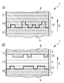
도 1A에는 전기적으로 펌핑되는 반도체 칩(1)의 실시 예가 도시되어 있다. 바람직하게 에피택셜 방식으로 성장된 상기 반도체 칩(1)은 p-측 연결부(p) 및 n-측 연결부(n)를 갖는다. 반도체 칩(1)의 용도에 따른 작동시, 상기 p-측 연결부(p)에는 포지티브 전압이 인가되고, n-측 연결부(n)에는 상기 p-측 연결부(p)에 상대적으로 네거티브 전압이 인가된다. 전자들과 같이 네거티브 전하 캐리어들은 반도체 칩(1)의 작동 중에 n-측 연결부(n)로부터 p-측 연결부(p)로 이동되고, 홀들과 같은 포지티브 전하 캐리어들은 p-측 연결부(p)로부터 n-측 연결부(n)로 이동된다. 상기 전하 캐리어들은 각각 상기 연결부들(p, n)을 통해서 반도체 칩(1) 내부로 주입된다.1A shows an embodiment of an electrically pumped semiconductor chip 1. The semiconductor chip 1 preferably grown epitaxially has a p-side connection portion p and an n-side connection portion n. A positive voltage is applied to the p-side connection portion p and a negative voltage is applied to the p-side connection portion p to the n-side connection portion n when the semiconductor chip 1 is operated according to the use of the semiconductor chip 1. [ do. Negative charge carriers, such as electrons, are moved from the n-side junction n to the p-side junction p during operation of the semiconductor chip 1 and positive charge carriers such as holes are injected from the p- side connection portion (n). The charge carriers are injected into the semiconductor chip 1 through the connection portions p and n, respectively.
반도체 칩(1)은 다수의 방사성 양자 웰(2)을 포함한다. 반도체 칩(1)의 작동 중에는, 전하 캐리어들의 재결합에 의해 상기 방사성 양자 웰들(2) 내에서 전자기 방사선이 발생된다. p-측 연결부(p) 방향으로, 예를 들면 성장 방향(G)으로 방사성 양자 웰들(2) 다음에는 각각 하나의 피복 층(4)이 배치되어 있다. 상기 피복 층(4)은 0.2㎚ 이상 0.5㎚ 이하, 바람직하게는 약 0.5㎚의 두께(T)를 갖는다. 피복 층(4)은 실제로 AlGaN으로 이루어지며, 이 경우 상기 피복 층(4)은 이종 원자 형태의 도펀트를 포함할 수 있다. 이 경우 피복 층(4)에서의 이종 원자 비율은 최대 0.01 원자-%이다.The semiconductor chip 1 includes a plurality of radioactive
방사성 양자 웰들(2)의 두께(Q)는 예컨대 1.5㎚ 이상 4.5㎚ 이하, 특히 약 3.5㎚이다. 이 경우 상기 양자 웰들(2)은 InGaN으로 이루어진다. 인듐 함량은 바람직하게 15% 이상 35% 이하이다. 다른 말로 표현하자면, 갈륨 격자 위치들의 15% 이상 35% 이하의 부분은 인듐 원자로 나타났다. The thickness Q of the
성장 방향(G)을 따라서, 피복 층들(4)과 방사성 양자 웰들(2) 사이에는 각각 하나의 배리어 층(5)이 존재한다. 상기 배리어 층(5)은 바람직하게 GaN으로 이루어진다. 상기 배리어 층들(5)도 마찬가지로 이종 원자 도펀트를 포함할 수 있다.There is one
이웃하는 2개의 피복 층(4) 간의 간격은 바람직하게 3㎚ 이상 8㎚ 이하, 특히 약 6㎚이다. 도 1A에 따른 실시 예의 경우에 상기 피복 층들(4)의 알루미늄 함량은 예를 들어 20% 이상 50% 이하이다.The distance between two neighboring covering layers 4 is preferably 3 nm or more and 8 nm or less, particularly about 6 nm. In the case of the embodiment according to FIG. 1A, the aluminum content of the covering layers 4 is, for example, 20% or more and 50% or less.
도 1B에는 성장 방향(G)을 따라서 밴드 갭(EG)의 프로파일이 개략적으로 도시되어 있다. 방사성 양자 웰들(2)의 영역에서 상기 밴드 갭(EG)은 예를 들어 약 2.55 eV이다. 피복 층들(4)의 영역에서 밴드 갭(EG)은 바람직하게 약 3.4 eV를 초과한다. 그러므로 피복 층들(4)에 의해 p-측 연결부(p) 쪽을 향하는 방사성 양자 웰들(2)의 p-측면에서는 밴드 갭(EG)의 국부적 상승 및 가전자대 구조물의 만곡이 수행된다. p-측면들에 있는 방사성 양자 웰들(2) 외부의 밴드 갭(EG)은 n-측 연결부(n) 쪽을 향하는 n-측면들에 있는 방사성 양자 웰들(2) 외부의 밴드 갭(EG)을 초과한다. 밴드 갭 구조물들의 이러한 만곡에 의해 홀들의 이동성이 상승되었다.1B schematically shows the profile of the band gap E G along the growth direction G. As shown in Fig. The band gap E G in the region of the
이로 인해 달성된 사실은, 특히 모든 방사성 양자 웰들(2)이 방사선 방출에 기여한다는 것이다. 이 경우 p-측 연결부(p)에 가장 가까운 양자 웰(2)이 가장 많은 비율의 방사선을 방출하며, 그에 반해 n측 연결부(n)에 가장 가까운 양자 웰(2)은 가장 적은 비율의 방사선을 방출한다. 각각의 방사성 양자 웰(2)은 바람직하게 적어도 2.5%의 반도체 칩(1)에 의해서 발생된 전체 방사선 출력을 방출한다.The fact that this is achieved, in particular, that all the
도 2에는 종래의 광전자 반도체 칩이 도시되어 있다(도 2A의 단면도 및 도 2B의 밴드 갭 구조물 참조). 성장 방향(G)으로 볼 때, 반도체 소자는 배리어 층들(5)과 양자 웰들(2) 사이의 시퀀스를 갖는다. 특히 도 2에 따른 반도체 소자에는 피복 층들(4)이 없기 때문에, 방사선의 방출에는 양자 웰들(2) 중 단 하나의 양자 웰만 도움이 될 수 있다. FIG. 2 shows a conventional optoelectronic semiconductor chip (see the cross-sectional view of FIG. 2A and the bandgap structure of FIG. 2B). In the growth direction G, the semiconductor device has a sequence between the barrier layers 5 and the
밴드 갭(EG)의 구조물은 양자 웰들(2)의 p-측면에서 밴드 갭의 상승을 갖지 않는다. 반대로 양자 웰의 n-측면에 비해 p-측면에서는 밴드 갭(EG)이 심지어 낮아진다.Structure of the band gap (E G) does not have an increase in the band gap in the p- side of the quantum wells (2). Conversely, the band gap (E G ) is even lower at the p-side than at the n-side of the quantum well.
도 3에 따른 반도체 칩(1)의 실시 예의 경우, 방사성 양자 웰들(2a 내지 2c)과 각각 할당된 피복 층들(4) 사이에는 각 하나씩의 중간층(3)이 존재한다. 상기 중간층(3)은 GaN으로 이루어지고, 양자 웰들(2), 피복 층들(4) 및 배리어 층들(5)과 마찬가지로 이종 원자의 도펀트를 포함할 수 있다. 중간층(3)의 두께는 바람직하게 1㎚보다 더 작다. 특히 상기 두께는 약 0.5㎚이다. 도 3에 따른 반도체 칩(1)에서 피복 층들(4)의 알루미늄 함량은 바람직하게 40% 이상 70% 이하이다.In the case of the embodiment of the semiconductor chip 1 according to Fig. 3, there is one
반도체 칩(1)은 바람직하게 3개 이상 20개 이하의 층 시퀀스(8)를 갖는다. 상기 층 시퀀스들(8)은 각각 추가의 중간층 없이 직접 인접한다. 각각의 층 시퀀스(8)는 하나의 방사성 양자 웰(2a 내지 2c), 하나의 중간층(3), 하나의 피복 층(4) 및 하나의 배리어 층(5)으로 이루어진다. 언급한 층들은 추가의 중간층들 없이 언급한 순서대로 직접 인접한다.The semiconductor chip 1 preferably has 3 to 20
다른 모든 실시 예와 마찬가지로 방사성 양자 웰들(2a 내지 2c)은 반도체 칩(1)의 작동 중에 서로 상이한 파장들(λ1, λ2, λ3)을 갖는 방사선을 각각 발생할 수 있다. 예를 들어 파장(λ1)은 약 440㎚이고, 파장(λ2)은 약 450㎚이며, 파장(λ3)은 약 465㎚이다. 이 경우 파장은 반도체 칩(1)의 작동 중에 최대 스펙트럼 출력 밀도가 방출되는 파장을 의미할 수 있다.As with all other embodiments, the
도 4A에는 반도체 칩(1)의 한 추가 실시 예의 개략적인 단면도가 도시되어 있으며, 상기 반도체 칩은 예컨대 도 1과 유사하게 설계될 수 있다. 도 4B에는 특히 도 3과 유사한 반도체 칩(1)의 상세도가 도시되어 있다.4A shows a schematic cross-sectional view of one further embodiment of the semiconductor chip 1, which may be designed, for example, similar to Fig. Fig. 4B shows a detailed view of the semiconductor chip 1, particularly similar to Fig.
반도체 칩(1)은 성장 방향(G)을 따라서 단분자층들(9)의 시퀀스를 갖는다. 상기 단분자층(9)은 성장 방향(G)에 수직 방향으로 연장되고, 각각 개별 단분자층(9) 내에 있는 원자들의 평균 원자 지름의 두께를 갖는다. 도 4A 및 도 4B에서는 단분자층들(9)이 파선에 의해 서로 한정된 반도체 칩(1)의 영역들로 표시되었다.The semiconductor chip 1 has a sequence of the
방사성 양자 웰(2)과 피복 층(4) 사이에는 전이 구역(24)이 있다(도 4A 참조). 상기 전이 구역(24)에는 재료 조성이 방사성 양자 웰(2)의 재료 조성에 상응하는 하부 영역들이 있다. 마찬가지로 재료 조성이 피복 층(4)의 조성에 상응하는 다른 하부 영역들도 존재한다. 도 4A에 따르면, 전이 영역(24)의 두께는 2개의 단분자층에 이른다.There is a
도 4B에 따른 실시 예에서, 방사성 양자 웰(2)과 중간층(3) 사이에 그리고 방사성 양자 웰(2)과 피복 층(4) 사이에 있는 전이 구역들(23, 24)은 각각 1개의 단분자층의 두께를 갖는다. 도 4A 및 도 4B와는 달리, 전이 영역들(23, 24, 34)의 바람직한 두께는 1개 이상 3개 이하의 단분자층일 수 있다. 전이 구역들(23, 24, 34)의 두께는 예컨대 투과 전자 현미경(TEM)을 통해서 측정될 수 있다.4B, the
다른 실시 예들에서도 마찬가지로, 반도체 칩(1)은 하나 또는 다수의 추가 (도면에는 도시되지 않은) 층들을 포함할 수 있다. 상기와 같은 층들은 터널 층들 또는 터널 전이부들, 전하 캐리어 차단 층들, 비방사성 양자 웰들, 전기 접촉 층들, 외부 층들 및/또는 광 파장 전도 층들일 수 있다. 마찬가지로 방사성 양자 웰들(2)은 각각 성장 방향(G)을 따라서 가변적인 인듐 함량을 포함할 수 있다. 따라서, 방사성 양자 웰들(2)은 도면에는 도시되지 않은 다수의 부분 층들을 포함할 수 있으며, 상기 부분 층들의 인듐 함량은 서로 상이하다.In other embodiments as well, the semiconductor chip 1 may include one or more additional layers (not shown in the figures). Such layers may be tunnel layers or tunnel transitions, charge carrier barrier layers, non-radioactive quantum wells, electrical contact layers, outer layers and / or optical waveguide conductive layers. Likewise, the
방사성 양자 웰들(2)의 개수 검출은, 예컨대 반도체 칩(1)에 공급되는 전류 세기에 대해 반도체 칩(1)에 의해 방출된 방사선의 파장 이동을 검출함으로써, 검출될 수 있다. 파장 이동이 크면 클수록, 방사성 양자 웰의 개수는 작다. 마찬가지로 반도체 칩(1)을 작동시키는 전류 세기에 대해, 방사성 양자 웰들의 내부 양자 효율을 규정함으로써, 방사성 양자 웰의 개수가 검출된다. The number detection of the
본 발명은 실시 예들을 참조하는 상세한 설명에 의해 한정되지 않는다. 오히려 본 발명은 각각의 새로운 특징 그리고 각각의 특징 조합을 포함하며, 상기 특징 또는 특징 조합 자체가 특허청구범위 또는 실시 예들에 명시적으로 기재되어 있지 않더라도, 특히 각각의 특징 조합은 특허청구범위에 포함된 것으로 간주한다.The present invention is not limited by the detailed description with reference to the embodiments. Rather, the present invention includes each new feature and each feature combination, and even if the feature or feature combination itself is not explicitly recited in the claims or embodiments, each feature combination is specifically included in the claims .
본 특허 출원서는 독일 특허 출원서 10 2009 037 416.7호를 우선권으로 주장하며, 상기 우선권 서류의 공개 내용은 본 출원서에 인용의 형태로 수용된다.This patent application claims priority from German Patent Application 10 2009 037 416.7, and the disclosure content of the priority document is accepted in the form of a citation in the present application.
Claims (12)
InGaN을 포함하거나 InGaN으로 이루어진 3개 내지 20개의 방사성 양자 웰들(2) 및
AlGaN을 포함하거나 AlGaN으로 이루어진 2개 이상의 피복 층들(4)
을 포함하며,
상기 피복 층들(4) 각각은 상기 방사성 양자 웰들(2) 중 정확히 하나의 방사성 양자 웰에 할당되어 있고,
상기 피복 층들(4)은 상기 방사성 양자 웰들(2)의 각 하나의 p-측면에 존재하며,
상기 방사성 양자 웰들(2)과 할당된 피복 층들(4) 간의 간격은 최대 1.5㎚이고,
상기 피복 층들(4)의 Al-함량은 20% 내지 70%이고,
GaN을 포함하거나 GaN으로 이루어진 2개 이상의 중간층들(3)을 더 포함하며,
상기 중간층들 각각은 상기 피복 층들(4)과 각각 할당된 방사성 양자 웰들(2) 사이에 있는,
광전자 반도체 칩.As an electrically pumped optoelectronic semiconductor chip 1,
3 to 20 radioactive quantum wells (2) containing InGaN or made of InGaN and
Two or more coating layers 4 comprising AlGaN or made of AlGaN,
/ RTI >
Each of said coating layers (4) is assigned to exactly one of said radioactive quantum wells (2)
The coating layers (4) are present at each one p-side of the radioactive quantum wells (2)
The spacing between the radioactive quantum wells 2 and the deposited coatings 4 is at most 1.5 nm,
The Al-content of the coating layers (4) is 20% to 70%
Further comprising two or more intermediate layers (3) comprising GaN or made of GaN,
Each of said intermediate layers being between said coating layers (4) and each assigned radioactive quantum well (2)
Optoelectronic semiconductor chip.
층 시퀀스(8)가 3번 내지 20번 반복되고,
이웃하는 층 시퀀스들(8)이 직접적으로 연속되며, 그리고
상기 층 시퀀스들(8)이
방사성 양자 웰(2),
GaN을 포함하거나 GaN으로 이루어진 중간층(3),
피복 층(4) 및
GaN을 포함하거나 GaN으로 이루어진 배리어 층(5)의 순서로 직접적으로 연속하는 층들로 이루어지고, 그리고
또한, 상기 피복 층들(4)의 두께가 0.5㎚ 내지 1.0㎚이며, 중간층들(3)의 두께가 0.4㎚ 내지 0.8㎚이며, 성장 방향으로 연속하는 2개의 피복 층(4)의 간격이 4㎚ 내지 6㎚인,
광전자 반도체 칩.The method according to claim 1,
The layer sequence 8 is repeated 3 to 20 times,
The neighboring layer sequences 8 are directly contiguous, and
The layer sequences 8
The radioactive quantum wells 2,
An intermediate layer 3 comprising GaN or made of GaN,
The coating layers (4) and
And a barrier layer 5 made of GaN or made of GaN.
The thickness of the coating layers 4 is 0.5 nm to 1.0 nm, the thickness of the intermediate layers 3 is 0.4 nm to 0.8 nm, the interval of the two coating layers 4 continuous in the growth direction is 4 nm To 6 nm,
Optoelectronic semiconductor chip.
상기 피복 층들(4)의 Al-함량은 40% 내지 70%인,
광전자 반도체 칩.The method according to claim 1,
The coating layer (4) has an Al-content of 40% to 70%
Optoelectronic semiconductor chip.
상기 피복 층들(4)의 두께 또는 평균 두께가 0.3㎚ 내지 1.5㎚인,
광전자 반도체 칩.The method according to claim 1,
Wherein the coating layers (4) have a thickness or an average thickness of 0.3 nm to 1.5 nm,
Optoelectronic semiconductor chip.
상기 중간층들(3)의 두께가 0.3㎚ 내지 1.2㎚이고, 상기 피복 층들(4)의 Al-함량은 40% 내지 70%인,
광전자 반도체 칩.The method according to claim 1,
Wherein the thickness of the intermediate layers (3) is 0.3 nm to 1.2 nm and the Al-content of the coating layers (4) is 40% to 70%
Optoelectronic semiconductor chip.
상기 방사성 양자 웰들(2), 피복 층들(4) 및 중간층들(3)의 전이 영역(23, 24, 34)이 1개 내지 3개의 단분자층의 두께를 갖는,
광전자 반도체 칩.The method according to claim 1,
Wherein the transition regions 23, 24 and 34 of the radioactive quantum wells 2, the coating layers 4 and the intermediate layers 3 have a thickness of one to three monolayers,
Optoelectronic semiconductor chip.
상기 방사성 양자 웰들(2)과 각각 할당된 피복 층들(4) 간의 간격이 최대 2개의 단분자층에 이르고, 상기 피복 층들(4)의 Al-함량이 20% 내지 50%인,
광전자 반도체 칩.The method according to any one of claims 1, 2, 4, 5, and 6,
Wherein the gap between the radioactive quantum wells 2 and the respective coated layers 4 reaches up to two monolayers and the Al-content of the coated layers 4 is 20% to 50%
Optoelectronic semiconductor chip.
성장 방향으로 연속하는 2개의 피복 층(4) 간의 간격이 3㎚ 내지 8㎚인,
광전자 반도체 칩.The method according to any one of claims 1, 3, 4, 5, and 6,
And the distance between the two coating layers (4) continuous in the growth direction is 3 nm to 8 nm,
Optoelectronic semiconductor chip.
상기 중간층들(3)의 평균 밴드 갭이 각각 할당된 방사성 양자 웰들(2)의 평균 밴드 갭의 적어도 120%인,
광전자 반도체 칩.7. The method according to any one of claims 1 to 6,
Wherein the average bandgap of the intermediate layers (3) is at least 120% of the average bandgap of the assigned radioactive quantum wells (2)
Optoelectronic semiconductor chip.
적어도 2개의 이웃하는 방사성 양자 웰(2)이 서로 상이한 평균 밴드 갭을 갖고, 상기 평균 밴드 갭의 편차는 0.03 eV 내지 0.20 eV인,
광전자 반도체 칩.7. The method according to any one of claims 1 to 6,
Wherein at least two neighboring radioactive quantum wells (2) have a different average bandgap from each other and the average bandgap deviation is from 0.03 eV to 0.20 eV.
Optoelectronic semiconductor chip.
InGaN을 포함하거나 InGaN으로 이루어진 2개 이상의 방사성 양자 웰들(2) 및
AlGaN을 포함하거나 AlGaN으로 이루어진 2개 이상의 피복 층들(4)
을 포함하며,
상기 피복 층들(4) 각각은 상기 방사성 양자 웰들(2) 중 정확히 하나의 방사성 양자 웰에 할당되어 있고,
상기 피복 층들(4)은 상기 방사성 양자 웰들(2)의 각 하나의 p-측면에 존재하며,
상기 방사성 양자 웰들(2)과 할당된 피복 층들(4) 간의 간격은 최대 1.5㎚이고,
상기 피복 층들(4)의 Al-함량은 20% 내지 70%이며, 그리고
상기 방사성 양자 웰들(2)의 밴드 갭이 각각 2.55 eV 내지 3.0 eV인,
광전자 반도체 칩.As an electrically pumped optoelectronic semiconductor chip 1,
Two or more radioactive quantum wells (2) comprising InGaN or made of InGaN and
Two or more coating layers 4 comprising AlGaN or made of AlGaN,
/ RTI >
Each of said coating layers (4) is assigned to exactly one of said radioactive quantum wells (2)
The coating layers (4) are present at each one p-side of the radioactive quantum wells (2)
The spacing between the radioactive quantum wells 2 and the deposited coatings 4 is at most 1.5 nm,
The Al-content of the coating layers (4) is 20% to 70%, and
Wherein the band gaps of the radioactive quantum wells (2) are 2.55 eV to 3.0 eV,
Optoelectronic semiconductor chip.
InGaN을 포함하거나 InGaN으로 이루어진 2개 이상의 방사성 양자 웰들(2) 및
AlGaN을 포함하거나 AlGaN으로 이루어진 2개 이상의 피복 층들(4)
을 포함하며,
상기 피복 층들(4) 각각은 상기 방사성 양자 웰들(2) 중 정확히 하나의 방사성 양자 웰에 할당되어 있고,
상기 피복 층들(4)은 상기 방사성 양자 웰들(2)의 각 하나의 p-측면에 존재하며,
상기 방사성 양자 웰들(2)과 할당된 피복 층들(4) 간의 간격은 최대 1.5㎚이고,
상기 피복 층들(4)의 Al-함량은 20% 내지 70%이고,
상기 방사성 양자 웰들(2)의 밴드 갭이 각각 2.55 eV 내지 3.0 eV이며,
이웃하는 방사성 양자 웰(2)이 서로 상이한 밴드 갭을 갖는,
광전자 반도체 칩.As an electrically pumped optoelectronic semiconductor chip 1,
Two or more radioactive quantum wells (2) comprising InGaN or made of InGaN and
Two or more coating layers 4 comprising AlGaN or made of AlGaN,
/ RTI >
Each of said coating layers (4) is assigned to exactly one of said radioactive quantum wells (2)
The coating layers (4) are present at each one p-side of the radioactive quantum wells (2)
The spacing between the radioactive quantum wells 2 and the deposited coatings 4 is at most 1.5 nm,
The Al-content of the coating layers (4) is 20% to 70%
The band gaps of the radioactive quantum wells 2 are 2.55 eV to 3.0 eV,
The neighboring radioactive quantum wells 2 have different band gaps from each other,
Optoelectronic semiconductor chip.
Applications Claiming Priority (3)
| Application Number | Priority Date | Filing Date | Title |
|---|---|---|---|
| DE102009037416.7 | 2009-08-13 | ||
| DE102009037416.7A DE102009037416B4 (en) | 2009-08-13 | 2009-08-13 | Electrically pumped optoelectronic semiconductor chip |
| PCT/EP2010/059291 WO2011018273A1 (en) | 2009-08-13 | 2010-06-30 | Electrically pumped optoelectronic semiconductor chip |
Related Parent Applications (1)
| Application Number | Title | Priority Date | Filing Date |
|---|---|---|---|
| KR1020127006584A Division KR101682345B1 (en) | 2009-08-13 | 2010-06-30 | Electrically pumped optoelectronic semiconductor chip |
Publications (2)
| Publication Number | Publication Date |
|---|---|
| KR20160142890A KR20160142890A (en) | 2016-12-13 |
| KR101733149B1 true KR101733149B1 (en) | 2017-05-08 |
Family
ID=42711811
Family Applications (2)
| Application Number | Title | Priority Date | Filing Date |
|---|---|---|---|
| KR1020127006584A KR101682345B1 (en) | 2009-08-13 | 2010-06-30 | Electrically pumped optoelectronic semiconductor chip |
| KR1020167033319A KR101733149B1 (en) | 2009-08-13 | 2010-06-30 | Electrically pumped optoelectronic semiconductor chip |
Family Applications Before (1)
| Application Number | Title | Priority Date | Filing Date |
|---|---|---|---|
| KR1020127006584A KR101682345B1 (en) | 2009-08-13 | 2010-06-30 | Electrically pumped optoelectronic semiconductor chip |
Country Status (7)
| Country | Link |
|---|---|
| US (1) | US8581236B2 (en) |
| EP (1) | EP2465148B1 (en) |
| JP (1) | JP5705222B2 (en) |
| KR (2) | KR101682345B1 (en) |
| CN (1) | CN102576785B (en) |
| DE (1) | DE102009037416B4 (en) |
| WO (1) | WO2011018273A1 (en) |
Families Citing this family (5)
| Publication number | Priority date | Publication date | Assignee | Title |
|---|---|---|---|---|
| TWI649895B (en) | 2010-04-30 | 2019-02-01 | 美國波士頓大學信託會 | High-efficiency ultraviolet light-emitting diode with variable structure position |
| US8723189B1 (en) | 2012-01-06 | 2014-05-13 | Trustees Of Boston University | Ultraviolet light emitting diode structures and methods of manufacturing the same |
| DE102013200507A1 (en) * | 2013-01-15 | 2014-07-17 | Osram Opto Semiconductors Gmbh | Optoelectronic semiconductor component |
| JP6010088B2 (en) * | 2014-11-07 | 2016-10-19 | 株式会社東芝 | Semiconductor light emitting device |
| JP2022172792A (en) * | 2021-05-07 | 2022-11-17 | 日機装株式会社 | Nitride semiconductor light emitting device |
Citations (2)
| Publication number | Priority date | Publication date | Assignee | Title |
|---|---|---|---|---|
| EP1667292A1 (en) | 2003-08-26 | 2006-06-07 | Sony Corporation | GaN III-V COMPOUND SEMICONDUCTOR LIGHT-EMITTING DEVICE AND METHOD FOR MANUFACTURING SAME |
| EP1883141A1 (en) | 2006-07-27 | 2008-01-30 | Osram Opto Semiconductors GmbH | LD or LED with superlattice cladding layer |
Family Cites Families (17)
| Publication number | Priority date | Publication date | Assignee | Title |
|---|---|---|---|---|
| US5023685A (en) * | 1988-06-06 | 1991-06-11 | Bethea Clyde G | Quantum-well radiation-interactive device, and methods of radiation detection and modulation |
| JP3304782B2 (en) * | 1996-09-08 | 2002-07-22 | 豊田合成株式会社 | Semiconductor light emitting device |
| JP3705047B2 (en) * | 1998-12-15 | 2005-10-12 | 日亜化学工業株式会社 | Nitride semiconductor light emitting device |
| DE19955747A1 (en) | 1999-11-19 | 2001-05-23 | Osram Opto Semiconductors Gmbh | Optical semiconductor device with multiple quantum well structure, e.g. LED, has alternate well layers and barrier layers forming super-lattices |
| JP4032636B2 (en) * | 1999-12-13 | 2008-01-16 | 日亜化学工業株式会社 | Light emitting element |
| US6586762B2 (en) * | 2000-07-07 | 2003-07-01 | Nichia Corporation | Nitride semiconductor device with improved lifetime and high output power |
| US6906352B2 (en) | 2001-01-16 | 2005-06-14 | Cree, Inc. | Group III nitride LED with undoped cladding layer and multiple quantum well |
| CN101834245B (en) * | 2001-06-15 | 2013-05-22 | 克里公司 | GaN based LED formed on a SiC substrate |
| US6927412B2 (en) | 2002-11-21 | 2005-08-09 | Ricoh Company, Ltd. | Semiconductor light emitter |
| JP2004289112A (en) * | 2003-03-06 | 2004-10-14 | Ricoh Co Ltd | Semiconductor light emitting element, its manufacturing method, optical transmitting module, optical transmitting/receiving module, and optical communication system |
| JP2006108585A (en) | 2004-10-08 | 2006-04-20 | Toyoda Gosei Co Ltd | Group iii nitride compound semiconductor light emitting element |
| JP2006210692A (en) * | 2005-01-28 | 2006-08-10 | Toyoda Gosei Co Ltd | Group iii nitride compound semiconductor light emitting device |
| JP2006332258A (en) * | 2005-05-25 | 2006-12-07 | Matsushita Electric Ind Co Ltd | Nitride semiconductor device and its manufacturing method |
| EP1764840A1 (en) * | 2005-09-15 | 2007-03-21 | SuperNova Optoelectronics Corporation | Gallium nitride semiconductor light emitting device |
| KR101345517B1 (en) * | 2006-09-01 | 2013-12-27 | 조지아 스테이트 유니버시티 리서치 파운데이션, 인크. | High operating temperature split-off band infrared detectors |
| KR101330898B1 (en) * | 2007-04-05 | 2013-11-18 | 엘지전자 주식회사 | Semiconductor laser diode |
| US20090183774A1 (en) * | 2007-07-13 | 2009-07-23 | Translucent, Inc. | Thin Film Semiconductor-on-Sapphire Solar Cell Devices |
-
2009
- 2009-08-13 DE DE102009037416.7A patent/DE102009037416B4/en active Active
-
2010
- 2010-06-30 EP EP10726134.9A patent/EP2465148B1/en active Active
- 2010-06-30 CN CN201080035921.1A patent/CN102576785B/en active Active
- 2010-06-30 KR KR1020127006584A patent/KR101682345B1/en active Application Filing
- 2010-06-30 WO PCT/EP2010/059291 patent/WO2011018273A1/en active Application Filing
- 2010-06-30 US US13/383,495 patent/US8581236B2/en active Active
- 2010-06-30 JP JP2012524169A patent/JP5705222B2/en active Active
- 2010-06-30 KR KR1020167033319A patent/KR101733149B1/en active IP Right Grant
Patent Citations (2)
| Publication number | Priority date | Publication date | Assignee | Title |
|---|---|---|---|---|
| EP1667292A1 (en) | 2003-08-26 | 2006-06-07 | Sony Corporation | GaN III-V COMPOUND SEMICONDUCTOR LIGHT-EMITTING DEVICE AND METHOD FOR MANUFACTURING SAME |
| EP1883141A1 (en) | 2006-07-27 | 2008-01-30 | Osram Opto Semiconductors GmbH | LD or LED with superlattice cladding layer |
Also Published As
| Publication number | Publication date |
|---|---|
| JP5705222B2 (en) | 2015-04-22 |
| JP2013502058A (en) | 2013-01-17 |
| EP2465148A1 (en) | 2012-06-20 |
| KR101682345B1 (en) | 2016-12-05 |
| US20120161103A1 (en) | 2012-06-28 |
| KR20160142890A (en) | 2016-12-13 |
| US8581236B2 (en) | 2013-11-12 |
| CN102576785B (en) | 2015-05-20 |
| EP2465148B1 (en) | 2017-08-09 |
| DE102009037416A1 (en) | 2011-02-17 |
| CN102576785A (en) | 2012-07-11 |
| KR20120045049A (en) | 2012-05-08 |
| WO2011018273A1 (en) | 2011-02-17 |
| DE102009037416B4 (en) | 2021-10-14 |
Similar Documents
| Publication | Publication Date | Title |
|---|---|---|
| KR100664985B1 (en) | Nitride based semiconductor device | |
| EP2673811B1 (en) | Light emitting device with dislocation bending structure | |
| KR100604406B1 (en) | Nitride semiconductor device | |
| US20080054247A1 (en) | Semiconductor layer structure with superlattice | |
| US20140225059A1 (en) | LED with Improved Injection Efficiency | |
| KR101733149B1 (en) | Electrically pumped optoelectronic semiconductor chip | |
| KR20090018688A (en) | Multiple quantum-well structure, radiation-emitting semiconductor base and radiation-emitting component | |
| US9722140B2 (en) | Optoelectronic semiconductor chip comprising a multi-quantum well comprising at least one high barrier layer | |
| US20120201264A1 (en) | Light emitting device with varying barriers | |
| US10522699B2 (en) | Optoelectronic semiconductor chip | |
| EP2919282B1 (en) | Nitride semiconductor stacked body and semiconductor light emitting device comprising the same | |
| US9634184B2 (en) | Optoelectronic semiconductor device | |
| KR102005236B1 (en) | Semiconductor light emitting device comprising contact layer for reflective layer | |
| US20080054252A1 (en) | Semiconductor layer structure with over lattice | |
| KR100558455B1 (en) | Nitride based semiconductor device | |
| US20150270439A1 (en) | Nitride Light Emitting Diode and Fabrication Method Thereof | |
| KR20140004361A (en) | Nitride semiconductor light emitting device using superlattice structure | |
| US8536603B2 (en) | Optoelectronic semiconductor chip and method of producing an optoelectronic semiconductor chip | |
| CN111108658B (en) | Laser diode | |
| KR101303589B1 (en) | Nitride semiconductor light emitting device and method for manufacturing thereof | |
| KR102199635B1 (en) | Optoelectronic components | |
| KR102597083B1 (en) | Aluminum nitride-aluminum oxide layer to improve the efficiency of group III nitride light emitting devices | |
| WO2016157739A1 (en) | Semiconductor light-emitting element | |
| KR20120055388A (en) | Nano rod light emitting device |
Legal Events
| Date | Code | Title | Description |
|---|---|---|---|
| A107 | Divisional application of patent | ||
| A201 | Request for examination | ||
| E902 | Notification of reason for refusal | ||
| E701 | Decision to grant or registration of patent right | ||
| GRNT | Written decision to grant |