KR101519490B1 - full bridge converter comprising switching cells and electronic device using the full bridge converter - Google Patents
full bridge converter comprising switching cells and electronic device using the full bridge converter Download PDFInfo
- Publication number
- KR101519490B1 KR101519490B1 KR1020130155411A KR20130155411A KR101519490B1 KR 101519490 B1 KR101519490 B1 KR 101519490B1 KR 1020130155411 A KR1020130155411 A KR 1020130155411A KR 20130155411 A KR20130155411 A KR 20130155411A KR 101519490 B1 KR101519490 B1 KR 101519490B1
- Authority
- KR
- South Korea
- Prior art keywords
- switching
- turned
- transistor switch
- coupling inductor
- transformer
- Prior art date
Links
Images


Classifications
-
- H—ELECTRICITY
- H02—GENERATION; CONVERSION OR DISTRIBUTION OF ELECTRIC POWER
- H02M—APPARATUS FOR CONVERSION BETWEEN AC AND AC, BETWEEN AC AND DC, OR BETWEEN DC AND DC, AND FOR USE WITH MAINS OR SIMILAR POWER SUPPLY SYSTEMS; CONVERSION OF DC OR AC INPUT POWER INTO SURGE OUTPUT POWER; CONTROL OR REGULATION THEREOF
- H02M1/00—Details of apparatus for conversion
- H02M1/0003—Details of control, feedback or regulation circuits
Landscapes
- Dc-Dc Converters (AREA)
Abstract
Description
본 발명은 풀 브릿지 컨버터 및 이를 이용하는 전자 장치에 대한 것으로, 보다 상세하게는 스위칭 셀을 포함하는 풀 브릿지 컨버터와 이를 이용하여 전압을 변경하여 사용하는 전자 장치에 대한 것이다. BACKGROUND OF THE
전자 기술의 발달에 힘입어 다양한 유형의 전자 장치들이 개발 및 보급되고 있다. 이러한 전자 장치들은 필수적으로 전원 장치를 이용한다. 오늘 날 전원 장치로는 절연형 DC-DC 컨버터가 많이 사용되고 있다.Various types of electronic devices have been developed and popularized by the development of electronic technology. These electronic devices essentially use a power supply. Today, isolated DC-DC converters are widely used as power supplies.
구체적으로는, 풀 브릿지 컨버터를 사용하여, 입력 전압을 필요한 크기의 전압으로 변압하는 전자 장치가 많이 사용되고 있다. Specifically, an electronic device for transforming an input voltage into a required voltage by using a full bridge converter is widely used.
풀 브릿지 컨버터는 대용량으로 갈수록 무게와 부피가 커진다. 이에 따라, 변압기가 전체 시스템 내에서 상당 부분을 차지하게 된다는 문제점이 있었다. Full-bridge converters become larger and heavier in weight and volume. As a result, there has been a problem that the transformer occupies a large portion in the entire system.
도 1은 종래의 일반적인 풀 브릿지 컨버터의 회로 구성을 나타내고, 도 2는 그 풀 브릿지 컨버터를 구동시키기 위한 스위칭 신호의 파형의 일 예를 나타낸다.FIG. 1 shows a circuit configuration of a conventional full bridge converter, and FIG. 2 shows an example of a waveform of a switching signal for driving the full bridge converter.
도 1에 따르면, 풀 브릿지 컨버터는 복수의 트랜지스터 스위치 및 다이오드들을 포함하는 입력부(10), 입력부(10)에 1차 권선이 연결된 트랜스포머(20), 트랜스포머(20)의 2차 권선에 연결된 출력부(30)를 포함한다.1, the full bridge converter includes an
입력부(10)에 포함된 각 트랜지스터 스위치(S1, S2, S3, S4)는 풀 브릿지 형태로 연결된다. 입력부(10)는 각 트랜지스터 스위치(S1, S2, S3, S4)의 스위칭 상태에 따라 서로 다른 크기의 전압(Vtr)을 트랜스포머(20)의 1차 권선에 인가한다. 트랜스포머(20)는 1차 권선 및 2차 권선 사이의 권선 비에 따라 전압(Vtr)을 변압하여 출력부(30)로 전달한다. 출력부(30)는 트랜스포머(20)의 2차 권선에서 출력된 전압을 정류하여 출력한다. Each of the transistor switches S1, S2, S3, and S4 included in the
도 2는 도 1의 회로에서 각 트랜지스터 스위치(S1, S2, S3, S4)를 제어하기 위한 제어 신호(a, b) 및 그에 따라 트랜스포머(20)의 1차 권선에 인가되는 전압(Vtr)의 크기(c)를 나타내는 도면이다. 도 2의 (a) 및 (b)에 도시된 바와 같이, 풀 브릿지 구조에서 서로 대응되는 스위치들(S1 및 S2, S3 및 S4)은 동시에 턴 온 될 수 없다. 이에 따라, S1 및 S4가 함께 턴 온된 구간에는, S2 및 S3은 턴 오프되고, S2 및 S3이 턴온될 때는 S1 및 S4가 턴오프된다. 2 is a graph showing the relationship between the control signals a and b for controlling each transistor switch S1, S2, S3 and S4 in the circuit of Fig. 1 and the voltage Vtr applied to the primary winding of the transformer 20 (C). Fig. As shown in Figs. 2 (a) and 2 (b), the switches S1 and S2, S3 and S4 corresponding to each other in the full bridge structure can not be turned on at the same time. Thus, in the section where S1 and S4 are turned on together, S2 and S3 are turned off, and when S2 and S3 are turned on, S1 and S4 are turned off.
이와 같이 복수의 스위치가 풀브릿지 형태로 연결된 경우, 노이즈로 인한 스위치의 단락 사고가 발생할 수 있다. 따라서, 턴 온 구간이 일부라도 겹치지 않도록, 전체 스위치가 턴오프되는 사이 구간을 형성할 수 있도록, 각 트랜지스터 스위치들(S1 및 S2, S3 및 S4)을 동시에 턴 오프시킨다. 따라서, 스위칭 주기와, 1차 권선에 인가하는 전압의 주기가 일치하게 된다. When a plurality of switches are connected in the form of a full bridge in this manner, a short circuit of the switch due to noise may occur. Therefore, the transistor switches S1 and S2, S3 and S4 are simultaneously turned off so that the entire turn-off period can be formed so that the turn-on period does not overlap at least partly. Therefore, the switching period and the period of the voltage applied to the primary winding coincide with each other.
한편, 스위칭 소자의 발달과 전원 장치의 소형화라는 현재의 추세에 따라 고주파 스위칭 기법이 풀 브릿지 컨버터에 많이 적용되고 있다. 이에 따라, 효율적인 고주파 스위칭이 가능한 풀 브릿지 컨버터에 대한 필요성이 대두되었다.On the other hand, according to the trend of development of switching devices and miniaturization of power supply devices, high frequency switching techniques are widely applied to full bridge converters. As a result, a need for a full bridge converter capable of efficient high frequency switching has emerged.
본 발명은 상술한 문제점을 해결하기 위한 것으로, 본 발명의 목적은 스위칭 셀을 이용하여 스위칭 주파수를 증대시킬 수 있는 풀 브릿지 컨버터 및 이를 이용하는 전자 장치를 제공함에 있다.SUMMARY OF THE INVENTION It is an object of the present invention to provide a full bridge converter capable of increasing a switching frequency by using a switching cell and an electronic device using the same.
이상과 같은 목적을 달성하기 위한 본 발명의 일 실시 예에 따르면, 풀 브릿지 컨버터는, 트랜스포머, 전압원에 대해 병렬적으로 연결된 제1 및 제2 스위칭부, 상기 트랜스포머의 1차 권선의 제1 단과 상기 제1 스위칭부 사이를 연결하는 제1 결합 인덕터 및 상기 트랜스포머의 상기 1차 권선의 제2 단과 상기 제2 스위칭부 사이를 연결하는 제2 결합 인덕터를 포함한다. 여기서, 상기 제1 및 제2 결합 인덕터는 상기 제1 및 제2 스위칭부의 스위칭 상태에 따라 상기 1차 권선에 상이한 크기의 전압을 인가한다. According to an aspect of the present invention, there is provided a full bridge converter including a transformer, first and second switching units connected in parallel with respect to a voltage source, first and second switching units connected to a first end of the primary winding of the transformer, A first coupling inductor for coupling between the first switching units, and a second coupling inductor for coupling between the second end of the primary winding of the transformer and the second switching unit. The first and second coupling inductors apply different voltages to the primary winding according to the switching states of the first and second switching units.
또한, 상기 제1 스위칭부는, 상기 전압원에 대해 병렬적으로 연결된 제1 및 제2 스위칭 셀을 포함하고, 상기 제2 스위칭 부는, 상기 전압원에 대해 병렬적으로 연결된 제3 및 제4 스위칭 셀을 포함할 수 있다. The first switching unit may include first and second switching cells connected in parallel to the voltage source, and the second switching unit may include third and fourth switching cells connected in parallel to the voltage source. can do.
여기서, 상기 제1 결합 인덕터는, 상기 제1 및 제2 스위칭 셀 사이에 형성되어, 상기 트랜스포머의 1차 권선의 상기 제1 단과 연결되며, 상기 제2 결합 인덕터는, 상기 제3 및 제4 스위칭 셀 사이에 형성되어, 상기 트랜스포머의 1차 권선의 상기 제2 단과 연결될 수 있다. Wherein the first coupling inductor is formed between the first and second switching cells and is connected to the first end of the primary winding of the transformer and the second coupling inductor is connected between the third and fourth switching cells, May be formed between the cells and connected to the second end of the primary winding of the transformer.
여기서, 상기 제1 스위칭 셀은, 상기 전압원에 연결된 제1 트랜지스터 스위치 및 상기 제1 트랜지스터 스위치에 직렬 연결된 제1 다이오드를 포함하고, 상기 제2 스위칭 셀은, 상기 전압원에 연결된 제2 트랜지스터 스위치 및 상기 제2 트랜지스터 스위치에 직렬 연결된 제2 다이오드를 포함하고, 상기 제3 스위칭 셀은, 상기 전압원에 연결된 제3 트랜지스터 스위치 및 상기 제3 트랜지스터 스위치에 직렬 연결된 제3 다이오드를 포함하며, 상기 제4 스위칭 셀은, 상기 전압원에 연결된 제4 트랜지스터 스위치 및 상기 제4 트랜지스터 스위치에 직렬 연결된 제4 다이오드를 포함할 수 있다.The first switching cell includes a first transistor switch connected to the voltage source and a first diode connected in series to the first transistor switch, the second switching cell includes a second transistor switch connected to the voltage source, Wherein the third switching cell comprises a third transistor switch coupled to the voltage source and a third diode connected in series to the third transistor switch, A fourth transistor switch coupled to the voltage source, and a fourth diode coupled in series to the fourth transistor switch.
또한, 상기 제1 결합 인덕터는, 상기 제1 트랜지스터 스위치 및 상기 제1 다이오드 사이에 형성되는 제1 노드와, 상기 제2 트랜지스터 스위치 및 상기 제2 다이오드 사이에 형성되는 제2 노드를 결합하여, 상기 제1 단과 연결하고, 상기 제2 결합 인덕터는, 상기 제3 트랜지스터 스위치 및 상기 제3 다이오드 사이에 형성되는 제3 노드와, 상기 제4 트랜지스터 스위치 및 상기 제4 다이오드 사이에 형성되는 제4 노드를 결합하여, 상기 제2 단과 연결할 수 있다. The first coupling inductor may include a first node formed between the first transistor switch and the first diode and a second node formed between the second transistor switch and the second diode, And the second coupling inductor includes a third node formed between the third transistor switch and the third diode and a fourth node formed between the fourth transistor switch and the fourth diode, And can be connected to the second end.
또한, 상기 제1, 제2 및 제4 트랜지스터 스위치가 턴 오프되고 상기 제3 트랜지스터 스위치가 턴 온되면, 상기 제1 결합 인덕터는 상기 전압원에서 공급되는 입력 전압의 1/2을 상기 제1 단에 인가하고, 상기 제2 결합 인덕터는 상기 입력 전압을 상기 제2 단에 인가하고, 상기 제1 및 제3 트랜지스터 스위치가 턴 온 되고 상기 제2 및 제3 트랜지스터 스위치가 턴 오프되면, 상기 제1 결합 인덕터는 상기 입력 전압을 상기 제1 단에 인가하고, 상기 제2 결합 인덕터는 상기 입력 전압을 상기 제2 단에 인가하며, 상기 제1 트랜지스터 스위치가 턴 온되고, 상기 제2, 제3 및 제4 트랜지스터 스위치가 턴 오프되면, 상기 제1 결합 인덕터는 상기 입력 전압을 상기 제1 단에 인가하고, 상기 제2 결합 인덕터는 상기 입력 전압의 1/2을 상기 제2 단에 인가하며, 상기 제1, 제2 및 제3 트랜지스터 스위치가 턴 온되고, 상기 제4 트랜지스터 스위치가 턴 오프되면, 상기 제1 결합 인덕터는 상기 입력 전압의 1/2을 상기 제1 단에 인가하고, 상기 제2 결합 인덕터는 상기 입력 전압을 상기 제2 단에 인가하며, 상기 제1, 제3 및 제4 트랜지스터 스위치가 턴 온되고, 상기 제2 트랜지스터 스위치가 턴 오프되면, 상기 제1 결합 인덕터는 상기 입력 전압을 상기 제1 단에 인가하고, 상기 제2 결합 인덕터는 상기 입력 전압의 1/2을 상기 제2 단에 인가할 수 있다.When the first, second and fourth transistor switches are turned off and the third transistor switch is turned on, the first coupling inductor converts 1/2 of the input voltage supplied from the voltage source to the first stage And the second coupling inductor applies the input voltage to the second end, and when the first and third transistor switches are turned on and the second and third transistor switches are turned off, The inductor applies the input voltage to the first end, the second coupling inductor applies the input voltage to the second end, the first transistor switch is turned on, and the second, third and When the four transistor switch is turned off, the first coupling inductor applies the input voltage to the first end, the second coupling inductor applies half of the input voltage to the second end, 1, the second and When the three transistor switch is turned on and the fourth transistor switch is turned off, the first coupling inductor applies half of the input voltage to the first end, and the second coupling inductor applies the input voltage And the first coupling inductor applies the input voltage to the first stage when the first, third and fourth transistor switches are turned on and the second transistor switch is turned off, And the second coupling inductor may apply one-half of the input voltage to the second stage.
한편, 본 발명의 일 실시 예에 따르면, 전자 장치는, 제1 및 제2 스위칭부를 포함하는 변압부 및 상기 제1 및 제2 스위칭부의 스위칭 상태를 각각 제어하여, 상기 변압부에서 출력되는 출력 전압의 크기를 조정하는 제어부를 포함한다. 여기서, 상기 변압부는, 트랜스포머, 상기 트랜스포머의 1차 권선의 제1 단과 상기 제1 스위칭부 사이를 연결하는 제1 결합 인덕터 및 상기 트랜스포머의 상기 1차 권선의 제2 단과 상기 제2 스위칭부 사이를 연결하는 제2 결합 인덕터를 포함할 수 있다. According to an embodiment of the present invention, an electronic device controls a switching state of a transformer including first and second switching units and a switching state of the first and second switching units, respectively, As shown in FIG. Here, the transformer may include a transformer, a first coupling inductor connecting the first end of the primary winding of the transformer and the first switching unit, and a second coupling inductor between the second end of the primary winding of the transformer and the second switching unit And a second coupling inductor for coupling the first and second coupling inductors.
이상과 같은 본 발명의 다양한 실시 예에 따르면, 기존의 컨버터에 비해 스위칭 주파수를 증대시킬 수 있다. According to various embodiments of the present invention as described above, the switching frequency can be increased as compared with the conventional converter.
도 1은 종래의 풀 브릿지 컨버터의 구성을 나타내는 도면,
도 2는 도 1의 풀 브릿지 컨버터의 동작을 설명하기 위한 도면,
도 3은 본 발명의 일 실시 예에 따른 풀 브릿지 컨버터의 구성을 나타내는 블럭도,
도 4는 도 3의 풀 브릿지 컨버터의 세부 구성을 설명하기 위한 회로도,
도 5는 도 4의 풀 브릿지 컨버터의 동작을 설명하기 위한 신호 파형도,
도 6 내지 도 10은 다양한 모드에 따른 풀 브릿지 컨버터의 동작을 설명하기 위한 도면,
도 11은 제1 결합 인덕터에 대한 등가 모형을 나타내는 도면,
도 12는 제1 결합 인덕터의 동작 특성을 설명하기 위한 신호 파형도,
도 13은 풀 브릿지 컨버터의 동작을 실험하기 위한 실험 조건의 일 예를 나타내는 도면,
도 14는 도 13의 실험 조건에 따라 실험한 풀 브릿지 컨버터의 동작 특성을 설명하기 위한 신호 파형도, 그리고,
도 15는 본 발명의 일 실시 예에 따른 전자 장치의 구성을 나타내는 블럭도이다. 1 is a diagram showing a configuration of a conventional full bridge converter,
FIG. 2 is a view for explaining the operation of the full bridge converter of FIG. 1,
3 is a block diagram showing the configuration of a full bridge converter according to an embodiment of the present invention.
Fig. 4 is a circuit diagram for explaining the detailed configuration of the full bridge converter of Fig. 3,
FIG. 5 is a signal waveform diagram for explaining the operation of the full bridge converter of FIG. 4,
6 to 10 are diagrams for explaining the operation of the full bridge converter according to various modes,
11 shows an equivalent model for a first coupling inductor,
12 is a signal waveform diagram for explaining the operation characteristics of the first coupling inductor,
13 is a diagram showing an example of an experimental condition for testing the operation of a full bridge converter,
FIG. 14 is a signal waveform diagram for explaining the operation characteristics of the full bridge converter tested according to the experimental conditions of FIG. 13,
15 is a block diagram showing the configuration of an electronic device according to an embodiment of the present invention.
이하에서, 첨부된 도면을 이용하여 본 발명에 대하여 구체적으로 설명한다.Hereinafter, the present invention will be described in detail with reference to the accompanying drawings.
도 3은 본 발명의 일 실시 예에 따른 풀 브릿지 컨버터의 구성을 나타내는 블럭도이다. 도 3에 따르면, 풀 브릿지 컨버터(100)는 스위칭부(110), 제1 결합 인덕터(120), 제2 결합 인덕터(130), 트랜스포머(140), 출력부(150)를 포함한다.3 is a block diagram illustrating the configuration of a full bridge converter according to an embodiment of the present invention. 3,
스위칭부(110)는 풀 브릿지 컨버터(100)에서 출력되는 전압을 조정하기 위한 스위칭 동작을 수행하는 부분이다. 스위칭부(110)는 제1 및 제2 스위칭부(111, 112)를 포함한다. The
제1 결합 인덕터(120)는 트랜스포머(140)의 1차 권선의 제1 단과, 제1 스위칭부(111)를 연결하고, 제2 결합 인덕터(130)는 트랜스포머(140)의 1차 권선의 제2 단과, 제2 스위칭부(112)를 연결한다.The
제1 및 제2 결합 인덕터(120, 130)는 제1 및 제2 스위칭부(111, 112)의 스위칭 상태에 따라 트랜스포머(140)의 1차 권선의 제1 단 및 제2 단에 상이한 크기의 전압을 인가한다. The first and
트랜스포머(140)는 1차 권선의 양단에 인가되는 전위차에 대응되는 출력 전압을 2차 권선을 통해 출력부(150)로 전달한다. 출력부(150)는 트랜스포머(140)의 2차 권선을 통해 전달되는 출력 전압을 정류하여, 출력한다.The
도 4는 도 3의 풀 브릿지 컨버터(100)의 세부 구성을 설명하기 위한 회로도이다. 도 4에 따르면, 제1 스위칭부(111) 및 제2 스위칭부(112)는 전압원(Vi)에 대해 병렬적으로 연결된다. 4 is a circuit diagram for explaining the detailed configuration of the
제1 스위칭부(111)는 두 개의 서로 다른 스위칭 셀(410, 420)을 포함한다. 제1 스위칭 셀(410) 및 제2 스위칭 셀(420)은 전압원(Vi)에 대해 병렬적으로 연결된다. 제1 스위칭 셀(410)에는 제1 트랜지스터 스위치(S1)가 포함되고, 제2 스위칭 셀(420)에는 제2 트랜지스터 스위치(S2)가 포함된다. 제1 스위칭 셀(410) 내에서 제1 트랜지스터 스위치(S1)에는 제1 다이오드(D1)가 직렬적으로 연결된다. 제2 스위칭 셀(420) 내에서 제2 트랜지스터 스위치(S2)에는 제2 다이오드(D2)가 직렬적으로 연결된다.The
제1 스위칭 셀(410)은 전압원(Vi)의 양극 단자가 제1 트랜지스터 스위치(S1)에 연결된 P 셀을 구성하고, 제2 스위칭 셀(420)은 전압원(Vi)의 음극 단자가 제2 트랜지스터 스위치(S2)에 연결된 N 셀을 구성한다. The
제2 스위칭부(112) 역시 두 개의 서로 다른 스위칭 셀(430, 440)을 포함한다. 제3 스위칭 셀(430) 및 제4 스위칭 셀(440)은 전압원(Vi)에 대해 병렬적으로 연결된다. 제3 스위칭 셀(430)에는 제3 트랜지스터 스위치(S3)가 포함되고, 제4 스위칭 셀(440)에는 제4 트랜지스터 스위치(S4)가 포함된다. 제3 스위칭 셀(430) 내에서 제3 트랜지스터 스위치(S3)에는 제3 다이오드(D3)가 직렬적으로 연결된다. 제4 스위칭 셀(440) 내에서 제4 트랜지스터 스위치(S4)에는 제4 다이오드(D4)가 직렬적으로 연결된다.The
제3 스위칭 셀(430) 및 제4 스위칭 셀(440) 역시, 제1 및 제2 스위칭 셀(410, 420)과 마찬가지로 각각 P 셀 및 N 셀을 구성한다.The
도 4에 도시된 바와 같이 제1 내지 제4 스위칭 셀(410 ~ 440)은 전압원에 대해 병렬적으로 연결된다. As shown in FIG. 4, the first to fourth switching
제1 결합 인덕터(120)는 제1 및 제2 스위칭 셀(410, 420) 사이에 형성되어, 트랜스포머(140)의 1차 권선의 제1 단(A노드)과 연결된다. 구체적으로는 제1 결합 인덕터(120)는 제1 트랜지스터 스위치(S1) 및 제1 다이오드(D1) 사이에 형성되는 제1 노드(C 노드)와 제2 트랜지스터 스위치(S2) 및 제2 다이오드(D2) 사이에 형성되는 제2 노드(D 노드)를 결합하여 제1 단(A 노드)과 연결된다.The
제2 결합 인덕터(130)는 제3 및 제4 스위칭 셀(430, 440) 사이에 형성되어, 트랜스포머(140)의 1차 권선의 제2 단(B 노드)과 연결된다. 구체적으로는 제2 결합 인덕터(130)는 제3 트랜지스터 스위치(S3) 및 제3 다이오드(D3) 사이에 형성되는 제3 노드(E 노드)와 제4 트랜지스터 스위치(S4) 및 제4 다이오드(D4) 사이에 형성되는 제4 노드(F 노드)를 결합하여 제2 단(B 노드)과 연결된다.The
따라서, 트랜스포머(140)의 1차 권선의 양단(A, B) 사이의 전위차는 A, B 노드 각각의 전압의 크기에 따라 결정된다. Therefore, the potential difference between the ends A and B of the primary winding of the
도 5는 복수의 트랜지스터 스위치(S1 ~ S4)를 제어하기 위한 제어 신호의 파형과, 그 제어 신호에 의해 회로 내의 각 노드에 인가되는 전압의 크기를 설명하기 위한 도면이다. 5 is a diagram for explaining the waveform of a control signal for controlling the plurality of transistor switches S1 to S4 and the magnitude of the voltage applied to each node in the circuit by the control signal.
먼저, 도 5의 (a), (b), (c), (d)는 각각 제1 내지 제4 트랜지스터 스위치(S1 ~ S4)에 인가되는 제어 신호의 파형을 나타낸다. 각 제어 신호에서 하이 값은 각 트랜지스터 스위치를 턴 온 시킬 수 있는 크기의 전압 값이 되고, 로우 값은 각 트랜지스터 스위치를 턴 온 시킬 수 있는 크기의 전압 값(예를 들어, 0V)이 된다. 5 (a), 5 (b), 5 (c) and 5 (d) show waveforms of control signals applied to the first to fourth transistor switches S1 to S4, respectively. In each control signal, a high value is a voltage value that can turn on each transistor switch, and a low value is a voltage value (for example, 0V) that can turn on each transistor switch.
각 제어 신호를 비교하면, 제1구간(①)에서는 제1, 제2 및 제4 트랜지스터 스위치(S1, S2, S4)는 턴오프되고, 제3 트랜지스터 스위치(S3)가 턴 온된다. 제2 구간(②), 제4 구간(④), 제6 구간(⑥), 제8 구간(⑧)에서는 제1 및 제3 트랜지스터 스위치(S1, S3)는 턴 온되고, 제2, 4 트랜지스터 스위치(S2, S4)가 턴 오프된다. 제3 구간(③)에서는 제1 트랜지스터 스위치(S1)만 턴 온되고, 제2, 3, 4 트랜지스터 스위치(S2, S3, S4)가 턴 오프된다. 제5 구간(⑤)에서는 제1, 2, 3 트랜지스터 스위치(S1, S2, S3)가 턴 온되고, 제4 트랜지스터 스위치(S4)가 턴 오프된다. 제7 구간(⑦)에서는 제1, 3, 4 트랜지스터 스위치(S1, S3, S4)가 턴 온되고, 제2 트랜지스터 스위치(S2)가 턴 오프된다.When the control signals are compared, the first, second and fourth transistor switches S1, S2 and S4 are turned off and the third transistor switch S3 is turned on in the first section (1). The first and third transistor switches S1 and S3 are turned on and the second and fourth transistors S1 and S3 are turned on in the second section (2), the fourth section (4), the sixth section (6) The switches S2 and S4 are turned off. In the third period (3), only the first transistor switch S1 is turned on and the second, third and fourth transistor switches S2, S3, S4 are turned off. In the fifth section (5), the first, second and third transistor switches (S1, S2, S3) are turned on and the fourth transistor switch (S4) is turned off. In the seventh section (⑦), the first, third and fourth transistor switches S1, S3 and S4 are turned on and the second transistor switch S2 is turned off.
도 5의 (e), (f)는 트랜스포머(140)의 1차 권선의 제1 단(A 노드)에 인가되는 전압(VAN), 트랜스포머(140)의 1차 권선의 제2 단(B 노드)에 인가되는 전압(VBN)을 나타내며, 도 5의 (g)는 트랜스포머(140)의 1차 권선에 인가되는 전압(VAB)을 나타낸다.5E and 5F show the voltage VAN applied to the first end (A node) of the primary winding of the
도 5의 (e)에 따르면, 제1 결합 인덕터(120)는 제1, 5 구간에서 입력 전압의 1/2를 출력하고, 나머지 구간에서 입력 전압을 그대로 출력하는 것을 알 수 있다. 도 5의 (f)에 따르면, 제2 결합 인덕터(13)는 제3, 7구간에서 입력 전압의 1/2를 출력하고, 나머지 구간에서 입력 전압을 그대로 출력하는 것을 알 수 있다.5E, it can be seen that the
이에 따라, 트랜스포머(140)의 1차 권선에 인가되는 전압(VAB)은 제1, 5 구간에서 -Vi/2 값을 가지고, 제3, 7 구간에서 Vi/2 값을 가지며, 나머지 구간에서 0 V 값을 가지는 3가지 레벨로 조정될 수 있다. 도 5의 (g)는 트랜스포머(140)의 1차 권선에 인가되는 전압값(VAB)을 나타내고, 도 5의 (h)는 트랜스포머(140)의 1차 권선으로 유입되는 전류(itr)의 변화 파형을 나타낸다. Accordingly, the voltage VAB applied to the primary winding of the
트랜스포머(140)는 1차 권선에 인가된 전압을 권선비(1:n)에 따라 변압한다. 이에 따라, 트랜스포머(140)의 2차 권선에는 n배 변화된 전압이 출력된다. 출력 전압은 출력부(150) 내의 LC 필터에 의해 정류된다. The
도 5의 (i)는 정류된 전압값(Vrec)을 나타낸다. 5 (i) shows the rectified voltage value Vrec.
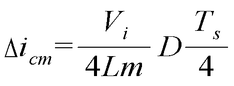
도 5의 (i)에서 D는 Ton/Ts' 값을 나타낸다. 여기서, Ton 은 Vrec이 nVi/2 값을 가지는 구간, Ts'는 Vrec의 한 주기(Ts/4)를 나타낸다. 따라서, Ton 구간의 시간은 DTs/4이다. 도 5의 (i)에 따르면, 정류된 전압값(Vrec)은 스위칭부를 제어하기 위한 제어 신호의 1주기(Ts)에 비해 1/4 주기(Ts/4)를 가짐을 알 수 있다. 즉, 본 풀 브릿지 컨버터(100)에 따르면, Vref에 인가되는 주파수는 스위칭 주파수의 4배의 주파수가 된다. 따라서, 출력 전류 리플은 1:1의 권선비인 경우, 기존의 컨버터에 비해 1/4배로 줄어든다. 또한, 출력단에 인가되는 주파수는 기존의 컨버터에 인가되는 주파수와 비교하면 2배가 된다. 이에 따라, 출력단에서 시스템 대역폭이 넓어져서, 부하의 갑작스러운 변화에 대해서도 빠르게 반응할 수 있다.In Fig. 5 (i), D represents the value of Ton / Ts'. Here, Ton denotes a period in which Vrec has a value of nVi / 2, and Ts' denotes one period (Ts / 4) of Vrec. Therefore, the time of Ton interval is DTs / 4. According to (i) of FIG. 5, it can be seen that the rectified voltage value Vrec has 1/4 period Ts / 4 compared to one period Ts of the control signal for controlling the switching unit. That is, according to the
이하에서는, 풀 브릿지 컨버터의 동작을 각 구간 별로 구체적으로 설명한다.Hereinafter, the operation of the full bridge converter will be described in detail for each section.
도 6은 제1 모드에 따른 풀 브릿지 컨버터의 동작을 나타내는 도면이다. 제1 모드란 상술한 제1 구간(①)에 해당하는 제어 신호들이 제1 내지 제4 트랜지스터 스위치(S1 ~ S4)로 인가되는 상태를 나타낸다. 6 is a diagram showing the operation of the full bridge converter according to the first mode. The first mode indicates a state in which the control signals corresponding to the first section (1) are applied to the first to fourth transistor switches S1 to S4.
이 경우, 제1 스위칭부(111) 내에서 제1 및 제2 트랜지스터 스위치(S1, S2)는 각각 턴 오프되고, 제2 스위칭부(112) 내에서 제3 다이오드(D3) 및 제4 트랜지스터 스위치(S4)가 턴 오프된다. 이에 따라, 트랜스포머(140)의 1차 권선의 제1 단(A노드)에 입력 전압(Vi)의 1/2이 인가되고, 트랜스포머(140)의 1차 권선의 제2 단(B노드)에 입력 전압(Vi)가 인가된다. 결과적으로, 1차 권선에는 -Vi/2의 전압이 인가된다. In this case, the first and second transistor switches S1 and S2 are turned off in the
출력부(150) 내에서는 전압 극성에 따라 제5 및 제8 다이오드(D5 및 D8)가 턴오프되고, 제6 및 제7 다이오드(D6 및 D7)가 턴온되어, LC 필터단에 Vrec가 인가된다. 도 5에서 설명한 바와 같이, Vrec는 nVi/2의 크기를 가진다. The fifth and eighth diodes D5 and D8 are turned off and the sixth and seventh diodes D6 and D7 are turned on according to the voltage polarity in the
도 7은 제2 모드에 따른 풀 브릿지 컨버터의 동작을 나타내는 도면이다. 제2 모드란 상술한 제2, 4, 6, 8 구간(②, ④, ⑥, ⑧)에 해당하는 제어 신호들이 제1 내지 제4 트랜지스터 스위치(S1 ~ S4)로 인가되는 상태를 나타낸다. 7 is a diagram showing the operation of the full bridge converter according to the second mode. The second mode is a state in which control signals corresponding to the second, fourth, sixth, and eighth sections (2, 4, 6, 8) are applied to the first to fourth transistor switches S1 to S4.
이 경우, 제1 및 제3 트랜지스터 스위치(S1, S3)는 각각 턴 온되고, 제2 및 제4 트랜지스터 스위치(S2 및 S4)가 턴 오프된다. 또한, 제1 및 제3 다이오드(D1 및 D3)도 턴 오프된다. 이에 따라, 트랜스포머(140)의 1차 권선 양단에는 입력 전압(Vi)이 그대로 인가된다. 결과적으로, 1차 권선에는 0 V의 전압이 인가되며, Vrec 또한 0 V 이 된다. In this case, the first and third transistor switches S1 and S3 are turned on, and the second and fourth transistor switches S2 and S4 are turned off. In addition, the first and third diodes D1 and D3 are also turned off. Thus, the input voltage Vi is applied to both ends of the primary winding of the
도 8은 제3 모드에 따른 풀 브릿지 컨버터의 동작을 나타내는 도면이다. 제3 모드란 상술한 제3 구간(③)에 해당하는 제어 신호들이 제1 내지 제4 트랜지스터 스위치(S1 ~ S4)로 인가되는 상태를 나타낸다.8 is a diagram showing the operation of the full bridge converter according to the third mode. The third mode is a state in which the control signals corresponding to the third period (3) are applied to the first to fourth transistor switches S1 to S4.
이 경우, 제1 트랜지스터 스위치(S1)만 턴 온되고, 제2, 3, 4 트랜지스터 스위치(S2, S3, S4)가 턴 오프된다. 또한, 제1 및 제3 다이오드(D1, D3)도 턴오프된다. 이에 따라, 트랜스포머(140)의 1차 권선의 제1 단(A노드)에 입력 전압(Vi)가 그대로 인가되고, 트랜스포머(140)의 1차 권선의 제2 단(B노드)에 입력 전압(Vi)의 1/2이 인가된다. 결과적으로, 1차 권선에는 Vi/2의 전압이 인가된다. In this case, only the first transistor switch S1 is turned on, and the second, third and fourth transistor switches S2, S3, and S4 are turned off. In addition, the first and third diodes D1 and D3 are also turned off. Thus, the input voltage Vi is directly applied to the first stage (node A) of the primary winding of the
출력부(150) 내에서는 전압 극성에 따라 제6 및 제7 다이오드(D6 및 D7)가 턴오프되고, 제5 및 제8 다이오드(D5 및 D8)가 턴온 되어, LC 필터단에 Vrec가 인가된다. 도 5에서 설명한 바와 같이, Vrec는 nVi/2의 크기를 가진다.The sixth and seventh diodes D6 and D7 are turned off and the fifth and eighth diodes D5 and D8 are turned on according to the voltage polarity in the
도 9는 제4 모드에 따른 풀 브릿지 컨버터의 동작을 나타내는 도면이다. 제4 모드란 상술한 제5 구간(⑤)에 해당하는 제어 신호들이 제1 내지 제4 트랜지스터 스위치(S1 ~ S4)로 인가되는 상태를 나타낸다.9 is a diagram showing the operation of the full bridge converter according to the fourth mode. The fourth mode is a state in which control signals corresponding to the fifth section (5) are applied to the first to fourth transistor switches S1 to S4.
이 경우, 제1, 2, 3 트랜지스터 스위치(S1, S2, S3)가 턴 온되고, 제4 트랜지스터 스위치(S4)가 턴 오프된다. 또한, 제1 내지 제3 다이오드(D1, D2, D3)도 턴오프된다. 이에 따라, 트랜스포머(140)의 1차 권선의 제1 단(A노드)에 입력 전압(Vi)의 1/2이 인가되고, 트랜스포머(140)의 1차 권선의 제2 단(B노드)에 입력 전압(Vi)이 인가된다. 결과적으로, 1차 권선에는 -Vi/2의 전압이 인가된다. In this case, the first, second and third transistor switches S1, S2 and S3 are turned on and the fourth transistor switch S4 is turned off. In addition, the first to third diodes D1, D2 and D3 are also turned off. Thus, one half of the input voltage Vi is applied to the first stage (A node) of the primary winding of the
출력부(150) 내에서는 전압 극성에 따라 제6 및 제7 다이오드(D6 및 D7)가 턴온되고, 제5 및 제8 다이오드(D5 및 D8)가 턴 오프 되어, LC 필터단에 Vrec가 인가된다. 도 5에서 설명한 바와 같이, Vrec는 nVi/2의 크기를 가진다.The sixth and seventh diodes D6 and D7 are turned on and the fifth and eighth diodes D5 and D8 are turned off according to the voltage polarity in the
도 10은 제5 모드에 따른 풀 브릿지 컨버터의 동작을 나타내는 도면이다. 제5 모드란 상술한 제7 구간(⑦)에 해당하는 제어 신호들이 제1 내지 제4 트랜지스터 스위치(S1 ~ S4)로 인가되는 상태를 나타낸다.10 is a diagram showing the operation of the full bridge converter according to the fifth mode. The fifth mode represents a state in which the control signals corresponding to the seventh section (7) are applied to the first to fourth transistor switches S1 to S4.
이 경우, 제1, 3, 4 트랜지스터 스위치(S1, S3, S4)가 턴 온되고, 제2 트랜지스터 스위치(S2)가 턴 오프된다. 또한, 제1, 3, 4 다이오드(D1, D2, D3)도 턴오프된다. 이에 따라, 트랜스포머(140)의 1차 권선의 제1 단(A노드)에 입력 전압(Vi)이 그대로 인가되고, 트랜스포머(140)의 1차 권선의 제2 단(B노드)에 입력 전압(Vi)의 1/2이 인가된다. 결과적으로, 1차 권선에는 Vi/2의 전압이 인가된다. In this case, the first, third and fourth transistor switches S1, S3 and S4 are turned on and the second transistor switch S2 is turned off. Also, the first, third and fourth diodes D1, D2 and D3 are also turned off. Thus, the input voltage Vi is directly applied to the first end (node A) of the primary winding of the
출력부(150) 내에서는 전압 극성에 따라 제6 및 제7 다이오드(D6 및 D7)가 턴 오프되고, 제5 및 제8 다이오드(D5 및 D8)가 턴 온 되어, LC 필터단에 Vrec가 인가된다. 도 5에서 설명한 바와 같이, Vrec는 nVi/2의 크기를 가진다.The sixth and seventh diodes D6 and D7 are turned off according to the voltage polarity in the
이상과 같이, 도 5에 도시된 바와 같은 제어 신호(a, b, c, d)가 한 주기(Ts)가 입력된다면, 풀 브릿지 컨버터(100)는 제1 모드, 제2 모드, 제3 모드, 제2 모드, 제4 모드, 제2 모드, 제5 모드, 제2 모드와 같이 순차적으로 상이한 모드로 변경되면서 동작한다. 이에 따라, 출력부(150)에서 출력되는 전압의 크기도 다양하게 변경될 수 있다. As described above, if one period (Ts) of the control signals (a, b, c, d) as shown in FIG. 5 is input, the
한편, 상술한 제1 및 제2 결합 인덕터(120, 130)는 서로 다른 크기의 인덕턴스를 가지는 코일들이 결합된 형태가 될 수 있다. 가령, 제1 결합 인덕터(120)가 L1 및 L2 인덕터가 결합된 형태라고 가정하면, 제1 결합 인덕터(120)는 도 11과 같은 등가 모델로 표현될 수 있다.Meanwhile, the first and
도 11에 따르면, 제1 결합 인덕터(120)는 제1 스위칭 셀(410) 및 제1 단(A 단)사이를 연결하는 제1 인덕터(L1)와, 제2 스위칭 셀(420) 및 제1 단(A 단)사이를 연결하는 제2 인덕터(L2) 및 그 사이를 연결하는 인덕터(Lt)로 모델링될 수 있다. 제1 인덕터(L1)로 유입되는 전류를 iL1, 제2 인덕터(L2)로 유입되는 전류를 iL2, 인덕터(L2)를 흐르는 전류를 icm이라고 하면, icm, iL1, iL2는 각각 다음과 같은 수식으로 표현될 수 있다. 11, the


여기서, iL1, iL2는 각각 0이상이며, icm은 itr/2 이상이다. Here, iL1 and iL2 are respectively 0 or more, and icm is at least itr / 2.
도 12는 제1 스위칭부(111)의 스위칭 상태에 따른 컨버터의 전류 파형의 변화를 설명하기 위한 도면이다. 도 12의 (a)는 인덕터(Lt)에 인가되는 전압, 즉, 도 4의 회로에서 C 노드 및 D 노드 사이의 전위차를 나타낸다. 도 12의 (a)에 따르면, 제1 및 제2 트랜지스터 스위치(S1, S2)가 오프되는 제1 구간에서는 C 노드 및 D 노드 사이에는 -Vi의 전압이 인가된다. 제1 및 제2 트랜지스터 스위치(S1, S2)가 모두 턴온되는 제5 구간에서는 C 노드 및 D 노드 사이에는 Vi의 전압이 인가된다.12 is a diagram for explaining the change of the current waveform of the converter in accordance with the switching state of the
도 12의 (b)는 인덕터(Lt)를 흐르는 전류 icm의 크기를 나타낸다. 도 12의 (b)에 따르면, icm은 제2, 3, 4구간에서는 로우값으로 고정되고, 제6, 7, 8 구간에서는 하이 값으로 고정된다. icm은 제1, 5구간에서는 로우값 또는 하이값으로 변화된다. 로우 값은 itr의 피크치 절대값의 1/2이 된다. 하이 값은 로우 값에 대해 Δicm을 더한 값이 된다. 12 (b) shows the magnitude of the current icm flowing through the inductor Lt. According to FIG. 12 (b), icm is fixed to a low value in the second, third and fourth sections, and to a high value in the sixth, seventh and eighth sections. icm is changed to a low value or a high value in the first and fifth sections. The low value is 1/2 of the absolute value of the peak value of itr. The high value is a value obtained by adding? Icm to the low value.
도 12의 (c)는 itr의 변화 파형, 도 12의 (d)는 iL1의 변화 파형, 도 12의 (e)는 출력부(150) 내의 인덕터(Lf)를 흐르는 전류 iLf의 변화 파형을 나타낸다.12C shows a change waveform of itr, Fig. 12D shows a change waveform of iL1, and Fig. 12E shows a change waveform of a current iLf flowing in the inductor Lf in the
icm, iLf의 변화값은 다음과 같은 수식으로 표현될 수 있다.The change values of icm and iLf can be expressed by the following equations.

상기 수식에서 D는 Ton/Ts'를 나타낸다. 이 경우, 전압 이득 Vo/Vi = nD/2가 될 수 있다. n은 1차, 2차 권선의 권선비를 나타낸다. In the above equation, D represents Ton / Ts'. In this case, the voltage gain Vo / Vi = nD / 2 can be obtained. n represents the turns ratio of the primary and secondary windings.
권선비가 1:1인 경우, 기존 컨버터에서의 iLf 변화량과, 본 컨버터에서의 iLf 변화량의 비는 1:4가 된다. When the winding ratio is 1: 1, the ratio of the iLf change amount in the conventional converter to the iLf change amount in this converter is 1: 4.
도 12와 같은 전류 파형을 고려하면, 풀 브릿지 컨버터를 용이하게 설계할 수 있다. Considering the current waveform as shown in FIG. 12, a full bridge converter can be easily designed.
도 13은 본 컨버터의 동작 특성을 판단하기 위하여 실험 조건의 일 예를 나타낸다. 도 13에 따르면, 제1 결합 인덕터(120) 내의 L1, L2는 각각 217μH이고, 출력부(150) 내의 인덕터(Lf)는 214μH, 커패시터(Cf)의 커패시턴스는 470μF, 저항은 5Ω, D는 0.8, Vi는 150V이며, 스위칭 주파수 fsw는 20kHz가 된다.FIG. 13 shows an example of experimental conditions for determining the operational characteristics of the converter. According to FIG. 13, L1 and L2 in the
도 14는 도 13과 같은 조건으로 실험한 제1 결합 인덕터의 동작 특성을 나타내는 도면이다. 도 14의 (a)는 트랜스포머(140)의 제1 단에 인가되는 전압 VAN의 크기를 나타내는 파형, 도 14의 (b)는 트랜스포머(140)의 1차 권선에 인가되는 전압 VAB의 크기를 나타내는 파형이다. 도 14의 (c)는 제1 결합 인덕터(120) 내의 제1 인덕터(L1)으로 유입되는 전류 iL1의 파형, 도 14의 (d)는 itr의 파형을 나타낸다.FIG. 14 is a graph showing the operating characteristics of the first coupling inductor tested under the same conditions as FIG. 13. FIG. 14A is a waveform showing the magnitude of the voltage VAN applied to the first end of the
이상 설명한 바와 같이, 풀 브릿지 컨버터는 복수의 결합 인덕터를 이용하여, 종래의 컨버터에 비해 2배의 크기를 가지는 주파수 신호로 구동될 수 있으며, 전압 크기는 줄어들게 되므로 변압기의 크기를 줄일 수 있다. 이에 따라, 기존 컨버터에 비해 필터의 부피를 줄일 수 있다. 또한, 암 쇼트, 암 오픈 등의 상황이 발생하더라도 문제없이 동작할 수 있어, 시스템 신뢰성이 향상될 수 있다. As described above, the full bridge converter can be driven with a frequency signal having a size twice as large as that of the conventional converter using a plurality of coupling inductors, and the size of the voltage can be reduced, so that the size of the transformer can be reduced. As a result, the volume of the filter can be reduced as compared with the conventional converter. In addition, even when a situation such as a female short or a female open occurs, it can be operated without a problem, and system reliability can be improved.
이상과 같은 풀 브릿지 컨버터는 다양한 전자 제품에 적용될 수 있다. Such a full bridge converter can be applied to various electronic products.
도 15는 본 발명의 일 실시 예에 따른 전자 장치의 구성을 나타내는 블럭도이다. 도 15에 따르면, 전자 장치(1500)는 변압부(100) 및 제어부(200)를 포함한다. 변압부(100)는 도 3 또는 도 4에서 설명한 바와 같은 풀 브릿지 컨버터로 구현될 수 있다. 변압부(100)에서 출력되는 전압은 전자 장치(1500) 내의 각 구성요소들로 제공될 수 있다. 15 is a block diagram showing the configuration of an electronic device according to an embodiment of the present invention. According to Fig. 15, the
구체적으로는, 전자 장치(1500)가 텔레비젼인 경우, 전자 장치(1500) 내에는 튜너, 비디오 프로세서, 오디오 프로세서, 디스플레이 패널, 백라이트 유닛 등과 같은 다양한 구성요소들이 포함될 수 있다. 이러한 구성요소들에서 소요되는 전압의 크기는 다양할 수 있다. 또는, 전자 장치(1500)가 PC인 경우, 냉각 팬, 메인 보드, 하드디스크 등과 같은 다양한 구성요소들이 포함될 수 있다. 이러한 구성요소들은 전자 장치(1500)의 종류에 따라 다양하게 변경될 수 있으며, 본 발명의 사상과는 직접적인 관련성이 없으므로, 이에 대한 도시 및 설명은 생략한다. Specifically, when the
제어부(200)는 변압부(100) 내의 제1 및 제2 스위칭부의 스위칭 상태를 각각 제어하여, 변압부(100)에서 출력되는 출력 전압의 크기를 조정할 수 있다. 이에 따라, 전자 장치(1500)내의 다양한 구성요소들에 대해 다양한 전압을 제공할 수 있다. The
상술한 바와 같이, 변압부(100) 내에는 제1 내지 제4 트랜지스터 스위치가 마련될 수 있으며, 제어부(200)는 제1 내지 제4 트랜지스터 스위치에 대해 다양한 제어 신호를 인가하여, 스위칭 상태를 제어할 수 있다. 구체적으로는, 제어부(200)는 도 5 내지 도 10에서 설명한 바와 같이, 다양한 모드로 동작할 수 있다. 각 모드 별 동작에 대해서는 상술한 부분에서 구체적으로 설명한 바 있으므로, 중복 설명은 생략한다.As described above, the first to fourth transistor switches may be provided in the
상술한 바와 같이 풀 브릿지 컨버터의 크기가 줄어들게 되면, 이를 이용한 전자 장치도 소형으로 구현할 수 있고, 에너비 효율도 올라가므로, 제조 비용 및 사용에 훨씬 더 유리하게 작용할 수 있다. If the size of the full bridge converter is reduced as described above, the electronic device using the full bridge converter can be reduced in size and the efficiency of the energy barrier can be increased.
이상에서는 본 발명의 바람직한 실시 예에 대하여 도시하고 설명하였지만, 본 발명은 상술한 특정의 실시 예에 한정되지 아니하며, 청구범위에서 청구하는 본 발명의 요지를 벗어남이 없이 당해 발명이 속하는 기술분야에서 통상의 지식을 가진자에 의해 다양한 변형실시가 가능한 것은 물론이고, 이러한 변형실시들은 본 발명의 기술적 사상이나 전망으로부터 개별적으로 이해되면 안 될 것이다. While the present invention has been particularly shown and described with reference to exemplary embodiments thereof, it is clearly understood that the same is by way of illustration and example only and is not to be construed as limiting the scope of the invention as defined by the appended claims. It will be understood by those skilled in the art that various changes and modifications may be made without departing from the spirit and scope of the present invention.
111 : 제1 스위칭부 112 : 제2 스위칭부
120 : 제1 결합 인덕터 130 : 제2 결합 인덕터
140 : 트랜스포머 150 : 출력부111: first switching unit 112: second switching unit
120: first coupling inductor 130: second coupling inductor
140: Transformer 150: Output section
Claims (6)
트랜스포머;
전압원에 대해 병렬적으로 연결된 제1 및 제2 스위칭부;
상기 트랜스포머의 1차 권선의 제1 단과 상기 제1 스위칭부 사이를 연결하는 제1 결합 인덕터; 및
상기 트랜스포머의 상기 1차 권선의 제2 단과 상기 제2 스위칭부 사이를 연결하는 제2 결합 인덕터;를 포함하며,
상기 제1 및 제2 결합 인덕터는 상기 제1 및 제2 스위칭부의 스위칭 상태에 따라 상기 1차 권선에 상이한 크기의 전압을 인가하고,
상기 제1 스위칭부는,
상기 전압원에 대해 병렬적으로 연결된 제1 및 제2 스위칭 셀을 포함하고,
상기 제2 스위칭 부는,
상기 전압원에 대해 병렬적으로 연결된 제3 및 제4 스위칭 셀을 포함하며,
상기 제1 결합 인덕터는,
상기 제1 및 제2 스위칭 셀 사이에 형성되어, 상기 트랜스포머의 1차 권선의 상기 제1 단과 연결되며,
상기 제2 결합 인덕터는,
상기 제3 및 제4 스위칭 셀 사이에 형성되어, 상기 트랜스포머의 1차 권선의 상기 제2 단과 연결되며,
상기 제1 스위칭 셀은,
상기 전압원에 연결되는 제1 트랜지스터 스위치; 및
상기 제1 트랜지스터 스위치에 직렬 연결된 제1 다이오드;를 포함하고,
상기 제2 스위칭 셀은,
상기 전압원에 연결되는 제2 트랜지스터 스위치; 및
상기 제2 트랜지스터 스위치에 직렬 연결된 제2 다이오드;를 포함하고,
상기 제3 스위칭 셀은,
상기 전압원에 연결되는 제3 트랜지스터 스위치; 및
상기 제3 트랜지스터 스위치에 직렬 연결된 제3 다이오드;를 포함하고,
상기 제4 스위칭 셀은,
상기 전압원에 연결되는 제4 트랜지스터 스위치; 및
상기 제4 트랜지스터 스위치에 직렬 연결된 제4 다이오드;를 포함하며,
상기 제1, 제2 및 제4 트랜지스터 스위치가 턴 오프되고 상기 제3 트랜지스터 스위치가 턴 온되면, 상기 제1 결합 인덕터는 상기 전압원에서 공급되는 입력 전압의 1/2을 상기 제1 단에 인가하고, 상기 제2 결합 인덕터는 상기 입력 전압을 상기 제2 단에 인가하고,
상기 제1 및 제3 트랜지스터 스위치가 턴 온 되고 상기 제2 및 제3 트랜지스터 스위치가 턴 오프되면, 상기 제1 결합 인덕터는 상기 입력 전압을 상기 제1 단에 인가하고, 상기 제2 결합 인덕터는 상기 입력 전압을 상기 제2 단에 인가하며,
상기 제1 트랜지스터 스위치가 턴 온되고, 상기 제2, 제3 및 제4 트랜지스터 스위치가 턴 오프되면, 상기 제1 결합 인덕터는 상기 입력 전압을 상기 제1 단에 인가하고, 상기 제2 결합 인덕터는 상기 입력 전압의 1/2을 상기 제2 단에 인가하며,
상기 제1, 제2 및 제3 트랜지스터 스위치가 턴 온되고, 상기 제4 트랜지스터 스위치가 턴 오프되면, 상기 제1 결합 인덕터는 상기 입력 전압의 1/2을 상기 제1 단에 인가하고, 상기 제2 결합 인덕터는 상기 입력 전압을 상기 제2 단에 인가하며,
상기 제1, 제3 및 제4 트랜지스터 스위치가 턴 온되고, 상기 제2 트랜지스터 스위치가 턴 오프되면, 상기 제1 결합 인덕터는 상기 입력 전압을 상기 제1 단에 인가하고, 상기 제2 결합 인덕터는 상기 입력 전압의 1/2을 상기 제2 단에 인가하는 것을 특징으로 하는 풀 브릿지 컨버터.In a full bridge converter,
Transformer;
First and second switching units connected in parallel to a voltage source;
A first coupling inductor connecting the first end of the primary winding of the transformer and the first switching unit; And
And a second coupling inductor connecting between the second end of the primary winding of the transformer and the second switching unit,
Wherein the first and second coupling inductors apply a voltage of a different magnitude to the primary winding according to the switching states of the first and second switching units,
Wherein the first switching unit comprises:
And first and second switching cells connected in parallel to the voltage source,
Wherein the second switching unit comprises:
And third and fourth switching cells connected in parallel to the voltage source,
Wherein the first coupling inductor comprises:
A second switching cell formed between the first and second switching cells and connected to the first end of the primary winding of the transformer,
Wherein the second coupling inductor comprises:
A third switching cell formed between the third and fourth switching cells and connected to the second end of the primary winding of the transformer,
Wherein the first switching cell comprises:
A first transistor switch coupled to the voltage source; And
And a first diode connected in series to the first transistor switch,
Wherein the second switching cell comprises:
A second transistor switch coupled to the voltage source; And
And a second diode connected in series to the second transistor switch,
Wherein the third switching cell comprises:
A third transistor switch coupled to the voltage source; And
And a third diode connected in series to the third transistor switch,
Wherein the fourth switching cell comprises:
A fourth transistor switch connected to the voltage source; And
And a fourth diode connected in series to the fourth transistor switch,
When the first, second and fourth transistor switches are turned off and the third transistor switch is turned on, the first coupling inductor applies 1/2 of the input voltage supplied from the voltage source to the first stage , The second coupling inductor applies the input voltage to the second stage,
Wherein when the first and third transistor switches are turned on and the second and third transistor switches are turned off, the first coupling inductor applies the input voltage to the first end, Applying an input voltage to said second stage,
When the first transistor switch is turned on and the second, third and fourth transistor switches are turned off, the first coupling inductor applies the input voltage to the first stage, and the second coupling inductor Applying a half of the input voltage to the second stage,
When the first, second and third transistor switches are turned on and the fourth transistor switch is turned off, the first coupling inductor applies 1/2 of the input voltage to the first stage, 2 coupling inductor applies the input voltage to the second stage,
When the first, third and fourth transistor switches are turned on and the second transistor switch is turned off, the first coupling inductor applies the input voltage to the first stage, and the second coupling inductor And a half of the input voltage is applied to the second stage.
상기 제1 결합 인덕터는,
상기 제1 트랜지스터 스위치 및 상기 제1 다이오드 사이에 형성되는 제1 노드와, 상기 제2 트랜지스터 스위치 및 상기 제2 다이오드 사이에 형성되는 제2 노드를 결합하여, 상기 제1 단과 연결하고,
상기 제2 결합 인덕터는,
상기 제3 트랜지스터 스위치 및 상기 제3 다이오드 사이에 형성되는 제3 노드와, 상기 제4 트랜지스터 스위치 및 상기 제4 다이오드 사이에 형성되는 제4 노드를 결합하여, 상기 제2 단과 연결하는 것을 특징으로 하는 풀 브릿지 컨버터.The method according to claim 1,
Wherein the first coupling inductor comprises:
A first node formed between the first transistor switch and the first diode and a second node formed between the second transistor switch and the second diode to connect with the first node,
Wherein the second coupling inductor comprises:
A third node formed between the third transistor switch and the third diode and a fourth node formed between the fourth transistor switch and the fourth diode are coupled to the second node, Full bridge converter.
제1 및 제2 스위칭부를 포함하는 변압부; 및
상기 제1 및 제2 스위칭부의 스위칭 상태를 각각 제어하여, 상기 변압부에서 출력되는 출력 전압의 크기를 조정하는 제어부;를 포함하며,
상기 변압부는,
트랜스포머;
상기 트랜스포머의 1차 권선의 제1 단과 상기 제1 스위칭부 사이를 연결하는 제1 결합 인덕터; 및
상기 트랜스포머의 상기 1차 권선의 제2 단과 상기 제2 스위칭부 사이를 연결하는 제2 결합 인덕터;를 포함하고,
상기 제1 스위칭부는,
전압원에 대해 병렬적으로 연결된 제1 및 제2 스위칭 셀을 포함하고,
상기 제2 스위칭부는,
전압원에 대해 병렬적으로 연결된 제3 및 제4 스위칭 셀을 포함하며,
상기 제1 결합 인덕터는,
상기 제1 및 제2 스위칭 셀 사이에 형성되어, 상기 트랜스포머의 1차 권선의 상기 제1 단과 연결되며,
상기 제2 결합 인덕터는,
상기 제3 및 제4 스위칭 셀 사이에 형성되어, 상기 트랜스포머의 1차 권선의 상기 제2 단과 연결되며,
상기 제1 스위칭 셀은,
상기 전압원에 연결되는 제1 트랜지스터 스위치; 및
상기 제1 트랜지스터 스위치에 직렬 연결된 제1 다이오드;를 포함하고,
상기 제2 스위칭 셀은,
상기 전압원에 연결되는 제2 트랜지스터 스위치; 및
상기 제2 트랜지스터 스위치에 직렬 연결된 제2 다이오드;를 포함하고,
상기 제3 스위칭 셀은,
상기 전압원에 연결되는 제3 트랜지스터 스위치; 및
상기 제3 트랜지스터 스위치에 직렬 연결된 제3 다이오드;를 포함하고,
상기 제4 스위칭 셀은,
상기 전압원에 연결되는 제4 트랜지스터 스위치; 및
상기 제4 트랜지스터 스위치에 직렬 연결된 제4 다이오드;를 포함하며,
상기 제1, 제2 및 제4 트랜지스터 스위치가 턴 오프되고 상기 제3 트랜지스터 스위치가 턴 온되면, 상기 제1 결합 인덕터는 상기 전압원에서 공급되는 입력 전압의 1/2을 상기 제1 단에 인가하고, 상기 제2 결합 인덕터는 상기 입력 전압을 상기 제2 단에 인가하고,
상기 제1 및 제3 트랜지스터 스위치가 턴 온 되고 상기 제2 및 제3 트랜지스터 스위치가 턴 오프되면, 상기 제1 결합 인덕터는 상기 입력 전압을 상기 제1 단에 인가하고, 상기 제2 결합 인덕터는 상기 입력 전압을 상기 제2 단에 인가하며,
상기 제1 트랜지스터 스위치가 턴 온되고, 상기 제2, 제3 및 제4 트랜지스터 스위치가 턴 오프되면, 상기 제1 결합 인덕터는 상기 입력 전압을 상기 제1 단에 인가하고, 상기 제2 결합 인덕터는 상기 입력 전압의 1/2을 상기 제2 단에 인가하며,
상기 제1, 제2 및 제3 트랜지스터 스위치가 턴 온되고, 상기 제4 트랜지스터 스위치가 턴 오프되면, 상기 제1 결합 인덕터는 상기 입력 전압의 1/2을 상기 제1 단에 인가하고, 상기 제2 결합 인덕터는 상기 입력 전압을 상기 제2 단에 인가하며,
상기 제1, 제3 및 제4 트랜지스터 스위치가 턴 온되고, 상기 제2 트랜지스터 스위치가 턴 오프되면, 상기 제1 결합 인덕터는 상기 입력 전압을 상기 제1 단에 인가하고, 상기 제2 결합 인덕터는 상기 입력 전압의 1/2을 상기 제2 단에 인가하는 것을 특징으로 하는 전자 장치.In an electronic device,
A transformer including first and second switching units; And
And a controller for controlling the switching states of the first and second switching units to adjust the magnitude of the output voltage output from the transforming unit,
The transformer
Transformer;
A first coupling inductor connecting the first end of the primary winding of the transformer and the first switching unit; And
And a second coupling inductor connecting between a second end of the primary winding of the transformer and the second switching unit,
Wherein the first switching unit comprises:
And first and second switching cells connected in parallel to the voltage source,
Wherein the second switching unit comprises:
And third and fourth switching cells connected in parallel to the voltage source,
Wherein the first coupling inductor comprises:
A second switching cell formed between the first and second switching cells and connected to the first end of the primary winding of the transformer,
Wherein the second coupling inductor comprises:
A third switching cell formed between the third and fourth switching cells and connected to the second end of the primary winding of the transformer,
Wherein the first switching cell comprises:
A first transistor switch coupled to the voltage source; And
And a first diode connected in series to the first transistor switch,
Wherein the second switching cell comprises:
A second transistor switch coupled to the voltage source; And
And a second diode connected in series to the second transistor switch,
Wherein the third switching cell comprises:
A third transistor switch coupled to the voltage source; And
And a third diode connected in series to the third transistor switch,
Wherein the fourth switching cell comprises:
A fourth transistor switch connected to the voltage source; And
And a fourth diode connected in series to the fourth transistor switch,
When the first, second and fourth transistor switches are turned off and the third transistor switch is turned on, the first coupling inductor applies 1/2 of the input voltage supplied from the voltage source to the first stage , The second coupling inductor applies the input voltage to the second stage,
Wherein when the first and third transistor switches are turned on and the second and third transistor switches are turned off, the first coupling inductor applies the input voltage to the first end, Applying an input voltage to said second stage,
When the first transistor switch is turned on and the second, third and fourth transistor switches are turned off, the first coupling inductor applies the input voltage to the first stage, and the second coupling inductor Applying a half of the input voltage to the second stage,
When the first, second and third transistor switches are turned on and the fourth transistor switch is turned off, the first coupling inductor applies 1/2 of the input voltage to the first stage, 2 coupling inductor applies the input voltage to the second stage,
When the first, third and fourth transistor switches are turned on and the second transistor switch is turned off, the first coupling inductor applies the input voltage to the first stage, and the second coupling inductor And applies 1/2 of the input voltage to the second stage.
Priority Applications (1)
| Application Number | Priority Date | Filing Date | Title |
|---|---|---|---|
| KR1020130155411A KR101519490B1 (en) | 2013-12-13 | 2013-12-13 | full bridge converter comprising switching cells and electronic device using the full bridge converter |
Applications Claiming Priority (1)
| Application Number | Priority Date | Filing Date | Title |
|---|---|---|---|
| KR1020130155411A KR101519490B1 (en) | 2013-12-13 | 2013-12-13 | full bridge converter comprising switching cells and electronic device using the full bridge converter |
Publications (1)
| Publication Number | Publication Date |
|---|---|
| KR101519490B1 true KR101519490B1 (en) | 2015-05-13 |
Family
ID=53394472
Family Applications (1)
| Application Number | Title | Priority Date | Filing Date |
|---|---|---|---|
| KR1020130155411A KR101519490B1 (en) | 2013-12-13 | 2013-12-13 | full bridge converter comprising switching cells and electronic device using the full bridge converter |
Country Status (1)
| Country | Link |
|---|---|
| KR (1) | KR101519490B1 (en) |
Citations (3)
| Publication number | Priority date | Publication date | Assignee | Title |
|---|---|---|---|---|
| US6504739B2 (en) * | 2001-05-18 | 2003-01-07 | Astec International Limited | Simple control circuit for synchronous rectifiers used in ZVS phase shifted full bridge converter |
| US6914788B2 (en) * | 2003-03-04 | 2005-07-05 | Sansha Electric Manufacturing Company, Limite | Power supply apparatus |
| US7423894B2 (en) * | 2006-03-03 | 2008-09-09 | Advanced Energy Industries, Inc. | Interleaved soft switching bridge power converter |
-
2013
- 2013-12-13 KR KR1020130155411A patent/KR101519490B1/en active IP Right Grant
Patent Citations (3)
| Publication number | Priority date | Publication date | Assignee | Title |
|---|---|---|---|---|
| US6504739B2 (en) * | 2001-05-18 | 2003-01-07 | Astec International Limited | Simple control circuit for synchronous rectifiers used in ZVS phase shifted full bridge converter |
| US6914788B2 (en) * | 2003-03-04 | 2005-07-05 | Sansha Electric Manufacturing Company, Limite | Power supply apparatus |
| US7423894B2 (en) * | 2006-03-03 | 2008-09-09 | Advanced Energy Industries, Inc. | Interleaved soft switching bridge power converter |
Non-Patent Citations (2)
| Title |
|---|
| IEEE 논문(제목: A Dual Bridge High Current DC-to-DC Converter with Soft Switching Capability), 논문발표 1997년 10월 5~9일 * |
| IEEE 논문(제목: A Dual Bridge High Current DC-to-DC Converter with Soft Switching Capability), 논문발표 1997년 10월 5~9일* |
Similar Documents
| Publication | Publication Date | Title |
|---|---|---|
| US20150061613A1 (en) | Dc-dc converter and method of controlling dc-dc converter | |
| US9543822B2 (en) | Over voltage protection control method and circuit for four-switch buck-boost converter | |
| JP6374261B2 (en) | Insulation synchronous rectification type DC / DC converter and synchronous rectification controller thereof, power supply device using the same, power supply adapter, and electronic device | |
| US9030049B2 (en) | Alternating current (AC) to direct current (DC) converter device | |
| KR101923754B1 (en) | Apparatus and method for efficient dc-to-dc conversion through wide voltage swings | |
| KR101520257B1 (en) | Bidirectional dc to dc converter and method for charging battery by using the same | |
| US8659281B2 (en) | Buck converter | |
| US10148176B2 (en) | DC to DC converter with pulse width modulation and a clamping circuit for non-pulse width modulation control | |
| US9608529B2 (en) | Converter and method for controlling the same | |
| US7352600B2 (en) | Electric power unit | |
| WO2019039487A1 (en) | Converter | |
| US7495935B2 (en) | DC/AC power converter and controlling method thereof | |
| US8076918B2 (en) | Multi-phase driving circuit with phase adjusting function | |
| US8817491B2 (en) | Electric power conversion system having an adaptable transformer turns ratio for improved efficiency | |
| JP2016116415A (en) | Insulation type dc-dc converter, power supply unit having the same, power supply adapter and electronic apparatus, and primary controller | |
| WO2019039489A1 (en) | Converter | |
| WO2019039488A1 (en) | Converter | |
| US7495421B2 (en) | Multi-phase buck converter | |
| US20150168983A1 (en) | Power conversion device, isolated driving circuit, and isolated driving method | |
| US10897211B2 (en) | Power conversion apparatus capable of performing step-up/step-down operation | |
| JP3346543B2 (en) | Switching power supply | |
| KR101519490B1 (en) | full bridge converter comprising switching cells and electronic device using the full bridge converter | |
| JP2018501770A (en) | DC-DC converter | |
| TWI543513B (en) | Resonant converter | |
| JP2004260887A (en) | Switching power supply unit |
Legal Events
| Date | Code | Title | Description |
|---|---|---|---|
| AMND | Amendment | ||
| AMND | Amendment | ||
| X701 | Decision to grant (after re-examination) | ||
| GRNT | Written decision to grant | ||
| FPAY | Annual fee payment |
Payment date: 20190429 Year of fee payment: 5 |