KR101233131B1 - Light-emitting device and electronic device - Google Patents
Light-emitting device and electronic device Download PDFInfo
- Publication number
- KR101233131B1 KR101233131B1 KR1020127000011A KR20127000011A KR101233131B1 KR 101233131 B1 KR101233131 B1 KR 101233131B1 KR 1020127000011 A KR1020127000011 A KR 1020127000011A KR 20127000011 A KR20127000011 A KR 20127000011A KR 101233131 B1 KR101233131 B1 KR 101233131B1
- Authority
- KR
- South Korea
- Prior art keywords
- layer
- oxide
- light emitting
- hole
- formed over
- Prior art date
Links
Images


Classifications
-
- H—ELECTRICITY
- H10—SEMICONDUCTOR DEVICES; ELECTRIC SOLID-STATE DEVICES NOT OTHERWISE PROVIDED FOR
- H10K—ORGANIC ELECTRIC SOLID-STATE DEVICES
- H10K50/00—Organic light-emitting devices
- H10K50/80—Constructional details
- H10K50/805—Electrodes
-
- H—ELECTRICITY
- H10—SEMICONDUCTOR DEVICES; ELECTRIC SOLID-STATE DEVICES NOT OTHERWISE PROVIDED FOR
- H10K—ORGANIC ELECTRIC SOLID-STATE DEVICES
- H10K50/00—Organic light-emitting devices
- H10K50/80—Constructional details
- H10K50/805—Electrodes
- H10K50/82—Cathodes
- H10K50/828—Transparent cathodes, e.g. comprising thin metal layers
-
- H—ELECTRICITY
- H10—SEMICONDUCTOR DEVICES; ELECTRIC SOLID-STATE DEVICES NOT OTHERWISE PROVIDED FOR
- H10K—ORGANIC ELECTRIC SOLID-STATE DEVICES
- H10K59/00—Integrated devices, or assemblies of multiple devices, comprising at least one organic light-emitting element covered by group H10K50/00
- H10K59/80—Constructional details
- H10K59/805—Electrodes
-
- H—ELECTRICITY
- H10—SEMICONDUCTOR DEVICES; ELECTRIC SOLID-STATE DEVICES NOT OTHERWISE PROVIDED FOR
- H10K—ORGANIC ELECTRIC SOLID-STATE DEVICES
- H10K30/00—Organic devices sensitive to infrared radiation, light, electromagnetic radiation of shorter wavelength or corpuscular radiation
- H10K30/80—Constructional details
- H10K30/81—Electrodes
-
- H—ELECTRICITY
- H10—SEMICONDUCTOR DEVICES; ELECTRIC SOLID-STATE DEVICES NOT OTHERWISE PROVIDED FOR
- H10K—ORGANIC ELECTRIC SOLID-STATE DEVICES
- H10K50/00—Organic light-emitting devices
- H10K50/10—OLEDs or polymer light-emitting diodes [PLED]
- H10K50/14—Carrier transporting layers
-
- H—ELECTRICITY
- H10—SEMICONDUCTOR DEVICES; ELECTRIC SOLID-STATE DEVICES NOT OTHERWISE PROVIDED FOR
- H10K—ORGANIC ELECTRIC SOLID-STATE DEVICES
- H10K50/00—Organic light-emitting devices
- H10K50/10—OLEDs or polymer light-emitting diodes [PLED]
- H10K50/14—Carrier transporting layers
- H10K50/15—Hole transporting layers
-
- H—ELECTRICITY
- H10—SEMICONDUCTOR DEVICES; ELECTRIC SOLID-STATE DEVICES NOT OTHERWISE PROVIDED FOR
- H10K—ORGANIC ELECTRIC SOLID-STATE DEVICES
- H10K50/00—Organic light-emitting devices
- H10K50/10—OLEDs or polymer light-emitting diodes [PLED]
- H10K50/14—Carrier transporting layers
- H10K50/16—Electron transporting layers
- H10K50/165—Electron transporting layers comprising dopants
-
- H—ELECTRICITY
- H10—SEMICONDUCTOR DEVICES; ELECTRIC SOLID-STATE DEVICES NOT OTHERWISE PROVIDED FOR
- H10K—ORGANIC ELECTRIC SOLID-STATE DEVICES
- H10K50/00—Organic light-emitting devices
- H10K50/80—Constructional details
- H10K50/85—Arrangements for extracting light from the devices
- H10K50/852—Arrangements for extracting light from the devices comprising a resonant cavity structure, e.g. Bragg reflector pair
-
- H—ELECTRICITY
- H10—SEMICONDUCTOR DEVICES; ELECTRIC SOLID-STATE DEVICES NOT OTHERWISE PROVIDED FOR
- H10K—ORGANIC ELECTRIC SOLID-STATE DEVICES
- H10K59/00—Integrated devices, or assemblies of multiple devices, comprising at least one organic light-emitting element covered by group H10K50/00
- H10K59/10—OLED displays
- H10K59/12—Active-matrix OLED [AMOLED] displays
-
- H—ELECTRICITY
- H10—SEMICONDUCTOR DEVICES; ELECTRIC SOLID-STATE DEVICES NOT OTHERWISE PROVIDED FOR
- H10K—ORGANIC ELECTRIC SOLID-STATE DEVICES
- H10K2102/00—Constructional details relating to the organic devices covered by this subclass
- H10K2102/10—Transparent electrodes, e.g. using graphene
- H10K2102/101—Transparent electrodes, e.g. using graphene comprising transparent conductive oxides [TCO]
- H10K2102/102—Transparent electrodes, e.g. using graphene comprising transparent conductive oxides [TCO] comprising tin oxides, e.g. fluorine-doped SnO2
-
- H—ELECTRICITY
- H10—SEMICONDUCTOR DEVICES; ELECTRIC SOLID-STATE DEVICES NOT OTHERWISE PROVIDED FOR
- H10K—ORGANIC ELECTRIC SOLID-STATE DEVICES
- H10K2102/00—Constructional details relating to the organic devices covered by this subclass
- H10K2102/10—Transparent electrodes, e.g. using graphene
- H10K2102/101—Transparent electrodes, e.g. using graphene comprising transparent conductive oxides [TCO]
- H10K2102/103—Transparent electrodes, e.g. using graphene comprising transparent conductive oxides [TCO] comprising indium oxides, e.g. ITO
-
- H—ELECTRICITY
- H10—SEMICONDUCTOR DEVICES; ELECTRIC SOLID-STATE DEVICES NOT OTHERWISE PROVIDED FOR
- H10K—ORGANIC ELECTRIC SOLID-STATE DEVICES
- H10K2102/00—Constructional details relating to the organic devices covered by this subclass
- H10K2102/301—Details of OLEDs
- H10K2102/351—Thickness
-
- Y—GENERAL TAGGING OF NEW TECHNOLOGICAL DEVELOPMENTS; GENERAL TAGGING OF CROSS-SECTIONAL TECHNOLOGIES SPANNING OVER SEVERAL SECTIONS OF THE IPC; TECHNICAL SUBJECTS COVERED BY FORMER USPC CROSS-REFERENCE ART COLLECTIONS [XRACs] AND DIGESTS
- Y02—TECHNOLOGIES OR APPLICATIONS FOR MITIGATION OR ADAPTATION AGAINST CLIMATE CHANGE
- Y02E—REDUCTION OF GREENHOUSE GAS [GHG] EMISSIONS, RELATED TO ENERGY GENERATION, TRANSMISSION OR DISTRIBUTION
- Y02E10/00—Energy generation through renewable energy sources
- Y02E10/50—Photovoltaic [PV] energy
- Y02E10/549—Organic PV cells
Abstract
본 발명의 목적은 투명 도전막 및 금속의 전기 부식이 방지될 수 있고 전극들의 쌍 사이에 발광 재료 및 투명 도전막을 포함하는 층을 가진 발광 소자를 제공하고, 발광 소자를 사용하는 발광 장치를 제공하는데 있다. 본 발명의 일 특징에 따르면, 발광 소자는 제1 전극(101)과 제2 전극(106) 사이에, 발광 재료를 포함하는 제1 층(102); 도너 레벨을 가진 재료를 포함하는 제2 층(103); 투명 도전막을 포함하는 제3 층(104); 및 홀-이송 매체를 포함하는 제4 층(105)을 포함하며; 제1 층(102), 제2 층(103), 제3 층(104), 제4 층(105) 및 제2 전극(106)은 순차적으로 설치되며, 제2 전극(106)은 금속을 포함하는 층을 가진다.SUMMARY OF THE INVENTION An object of the present invention is to provide a light emitting device having a layer comprising a light emitting material and a transparent conductive film between a pair of electrodes which can prevent electrical corrosion of a transparent conductive film and a metal, and to provide a light emitting device using the light emitting device. have. According to one feature of the invention, the light emitting device comprises: a first layer (102) comprising a light emitting material between the first electrode (101) and the second electrode (106); A second layer 103 comprising a material having a donor level; A third layer 104 comprising a transparent conductive film; And a fourth layer 105 comprising a hole-transport medium; The first layer 102, the second layer 103, the third layer 104, the fourth layer 105 and the second electrode 106 are sequentially installed, and the second electrode 106 includes a metal. To have a layer.
Description
본 발명은 전계를 인가시켜 발광할 수 있는 유기 화합물을 포함하는 층과 전극들의 쌍을 가지는 발광 소자에 관한 것이다. 또한, 본 발명은 발광 소자를 가지는 발광 장치에 관한 것이다.The present invention relates to a light emitting device having a layer and a pair of electrodes including an organic compound capable of emitting light by applying an electric field. The present invention also relates to a light emitting device having a light emitting element.
발광 재료를 사용하는 발광 소자는 박막, 경량, 고속 응답, DC 저전압 드라이브 등의 장점을 가지며 차세대 평판 디스플레이에 적용될 것이다. 더욱이, 매트릭스로 배치된 발광 소자들을 가진 발광 장치는 넓은 시야각 및 높은 가시성에 있어서 종래의 액정 표시 장치에 비하여 우수하다고 한다.Light emitting devices using light emitting materials have advantages such as thin film, light weight, high speed response, DC low voltage drive, and will be applied to next generation flat panel displays. Moreover, light emitting devices having light emitting elements arranged in a matrix are said to be superior to conventional liquid crystal displays in a wide viewing angle and high visibility.
발광 소자는 이하의 발광 메커니즘, 즉 전극들의 쌍 사이에 끼워진 발광층에 전압이 공급되고, 제2 전극으로부터 주입된 전자들 및 제1 전극으로부터 주입된 홀들이 분자 여기자들을 형성하기 위하여 발광층의 발광 중심에서 재결합되며, 분자 여기자들이 접지상태로 리턴될 때 에너지를 해제함으로써 발광되는 발광 메커니즘을 가진다. 여기 상태로서 단일항 여기 상태 및 삼중항 여기 상태가 각각 알려져 있으며, 상기 여기 상태들 중 어느 하나를 통해 가능한 발광이 고려된다.The light emitting device has the following light emitting mechanism, that is, voltage is supplied to the light emitting layer sandwiched between the pair of electrodes, and electrons injected from the second electrode and holes injected from the first electrode are formed at the emission center of the light emitting layer to form molecular excitons. It has a light emitting mechanism that recombines and emits light by releasing energy when molecular excitons return to ground. As the excited state, singlet excited state and triplet excited state are respectively known, and possible light emission through any one of the above excited states is considered.
발광 소자의 특징을 강화시키기 위하여, 소자 구조의 개선 및 재료의 개발 등이 수행된다.In order to enhance the characteristics of the light emitting device, improvement of the device structure, development of materials, and the like are performed.
예컨대, 발광부와 반사 금속 사이에 ITO를 끼움으로써 발광부로부터 반사 전극까지의 광학 길이 L이 제어되는 방법은, 발광부로부터 반사 금속까지의 거리를 제어함으로써 휘도를 저하시키지 않고 외부 양자 효율성을 증가시키는 수단으로서 제공된다(예컨대, 참조문헌 1: 일본 특허출원 공개번호 제2003-272855호 참조).For example, the method in which the optical length L from the light emitting portion to the reflective electrode is controlled by sandwiching ITO between the light emitting portion and the reflective metal increases the external quantum efficiency without lowering the luminance by controlling the distance from the light emitting portion to the reflective metal. (See, for example, reference 1: Japanese Patent Application Laid-open No. 2003-272855).
도 2는 참조문헌 1에 개시된 소자 구조를 개략적으로 도시한다. 이러한 구조에서는 투명 전극(201), 발광부(202), 투명 도전막(203) 및 금속 전극(204)이 적층된다. 투명 도전막(203)의 두께를 조절함으로써, 발광부으로부터 금속 전극까지의 광학 길이 L은 외부 양자 효율성을 증가시키도록 최적화된다.2 schematically illustrates the device structure disclosed in
그러나, 참조문헌 1에 개시된 구조에 따르면, 투명 도전막(203)과 반사 금속(금속 전극)(204)이 접하기 때문에, 부식 문제가 존재한다. 여기서, 자체 전위차 등으로 인하여 부식이 발생한다는 것이 알려져 있으며, 또한 부식은 전기 부식으로 언급된다(예컨대, 참조문헌 2: 일본특허출원 공개번호 제2003-89864호 참조). 참조문헌 2는 3.5%의 염화나트륨 용액(27℃의 액체 온도)을 사용하고 그리고 기준 전극으로서 은/은-염화물을 사용하여 측정된 자체 전위를 개시한다. 이러한 측정의 경우에, 고반사율을 가진 금속으로서 알려진 알루미늄의 자체 전위는 대략 -1550 mV인 반면에, 투명 도전막(SnO2를 10중량%로 포함하는 In2O3)으로서 사용되는 ITO의 자체 전위는 대략 -1000mV이다. 따라서, 알루미늄과 ITO의 자체 전위들 간의 차는 크다. 따라서, 알루미늄과 ITO가 서로 접하도록 적층될 때, 알루미늄과 ITO 간의 적층 인터페이스에서 산화물-감소 반응이 진행될 것이며, 이에 따라 전기 부식이 매우 발생한다. 이러한 전기 부식의 문제점은 ITO 및 알루미늄의 결합과 무관하게 발생된다.However, according to the structure disclosed in
자체 전위는 전류가 외부로부터 공급되지 않은 상태에서 임의의 용액에서 반응이 이루어질 때 기준 전극에 대한 반응 전위, 즉 폐루프(closed loop)의 전위이며, 휴면 전위로서 언급된다. The self potential is the reaction potential for the reference electrode, i.e. the closed loop, when the reaction takes place in any solution with no current supplied from the outside and is referred to as the sleep potential.
전술한 문제점들을 감안하여, 본 발명의 목적은 전극들의 쌍 사이에 발광 재료 및 투명 도전막을 포함하는 층을 가진 발광 소자를 제공하는데 있으며, 투명 도전막 및 금속의 전기 부식이 방지될 수 있다. 더욱이, 본 발명의 목적은 발광 소자를 사용하는 발광 장치를 제공하는데 있다. In view of the above problems, it is an object of the present invention to provide a light emitting device having a layer comprising a light emitting material and a transparent conductive film between a pair of electrodes, wherein the electrical corrosion of the transparent conductive film and metal can be prevented. Furthermore, an object of the present invention is to provide a light emitting device using the light emitting element.
전술한 문제점들을 해결한 본 발명에 따른 발광 소자의 한 구조에 따르면, 발광 소자는 제1 전극과 제2 전극 사이에, 발광 재료를 포함하는 제1 층; 유기 화합물 및 전자-공급 재료를 포함하는 제2 층; 투명 도전막을 포함하는 제3 층; 및 홀-이송 매체를 포함하는 제4 층을 포함하며; 발광 재료를 포함하는 제1 층, 유기 화합물 및 전자-공급 재료를 포함하는 제2 층, 투명 도전막을 포함하는 제3 층, 홀-이송 매체를 포함하는 제4 층, 및 제2 전극은 순차적으로 설치되며, 제2 전극은 금속을 포함하는 층을 가진다.According to a structure of a light emitting device according to the present invention which solves the above problems, the light emitting device comprises: a first layer comprising a light emitting material between the first electrode and the second electrode; A second layer comprising an organic compound and an electron-supply material; A third layer comprising a transparent conductive film; And a fourth layer comprising a hole-transport medium; A first layer comprising a luminescent material, a second layer comprising an organic compound and an electron-supply material, a third layer comprising a transparent conductive film, a fourth layer comprising a hole-transporting medium, and a second electrode are sequentially And the second electrode has a layer comprising a metal.
전술한 문제점들을 해결한 본 발명에 따른 발광 소자의 다른 구조에 따르면, 발광 소자는 제1 전극과 금속을 포함하는 제2 전극 사이에, 발광 재료를 포함하는 제1 층; 유기 화합물 및 전자-공급 재료를 포함하는 제2 층; 투명 도전막을 포함하는 제3 층; 및 홀-이송 매체를 포함하는 제4 층을 포함하며; 발광 재료를 포함하는 제1 층, 유기 화합물 및 전자-공급 재료를 포함하는 제2 층, 투명 도전막을 포함하는 제3 층, 홀-이송 매체를 포함하는 제4 층 및 제2 전극은 순차적으로 설치된다.According to another structure of the light emitting device according to the present invention which solves the above-mentioned problems, the light emitting device comprises: a first layer comprising a light emitting material between the first electrode and the second electrode comprising a metal; A second layer comprising an organic compound and an electron-supply material; A third layer comprising a transparent conductive film; And a fourth layer comprising a hole-transport medium; A first layer comprising a luminescent material, a second layer comprising an organic compound and an electron-supply material, a third layer comprising a transparent conductive film, a fourth layer comprising a hole-transporting medium and a second electrode are sequentially installed do.
전술한 문제점들을 해결한 본 발명에 따른 발광 소자의 또 다른 구조에 따르면, 발광 소자를 사용하는 발광 장치는 제1 전극과 제2 전극 사이에, 발광 재료를 포함하는 제1 층; 도너 레벨(donor level)을 가진 재료를 포함하는 제2 층; 투명 도전막을 포함하는 제3 층; 및 홀-이송 매체를 포함하는 제4 층을 포함하며; 발광 재료를 포함하는 제1 층, 도너 레벨을 가진 재료를 포함하는 제2 층, 투명 도전막을 포함하는 제3 층, 홀-이송 매체를 포함하는 제4 층 및 제2 전극은 순차적으로 설치되며, 제2 전극은 금속을 포함하는 층을 갖는다.According to yet another structure of a light emitting device according to the present invention that solves the above problems, a light emitting device using a light emitting device comprises: a first layer comprising a light emitting material between the first electrode and the second electrode; A second layer comprising a material having a donor level; A third layer comprising a transparent conductive film; And a fourth layer comprising a hole-transport medium; A first layer comprising a luminescent material, a second layer comprising a material having a donor level, a third layer comprising a transparent conductive film, a fourth layer comprising a hole-transporting medium and a second electrode are sequentially installed, The second electrode has a layer comprising a metal.
전술한 문제점들을 해결한 본 발명에 따른 발광 소자의 또 다른 구조에 따르면, 발광 소자는 제1 전극과 금속을 포함하는 제2 전극 사이에, 발광 재료를 포함하는 제1 층; 도너 레벨을 가진 재료를 포함하는 제2 층; 투명 도전막을 포함하는 제3 층; 및 홀-이송 매체를 포함하는 제4 층을 포함하며; 발광 재료를 포함하는 제1 층, 도너 레벨을 가진 재료를 포함하는 제2 층, 투명 도전막을 포함하는 제3 층, 홀-이송 매체를 포함하는 제4 층 및 제2 전극은 순차적으로 제공된다.According to another structure of the light emitting device according to the present invention to solve the above problems, the light emitting device comprises: a first layer comprising a light emitting material between the first electrode and the second electrode comprising a metal; A second layer comprising a material having a donor level; A third layer comprising a transparent conductive film; And a fourth layer comprising a hole-transport medium; A first layer comprising a luminescent material, a second layer comprising a material having a donor level, a third layer comprising a transparent conductive film, a fourth layer comprising a hole-transporting medium and a second electrode are provided sequentially.
전술한 구조에 있어서, 유기 화합물 및 전자-공급 재료를 포함하는 제2 층 및 홀-이송 매체를 포함하는 제4 층의 각각은 단층 구조 또는 다수의 층들이 적층되는 다층 구조로 형성될 수 있다. 여기서, 유기 화합물은 바람직하게 전자 이송 능력을 가진 유기 화합물, 특히 π-공액 골격을 포함하는 배위자(ligand)를 가진 금속 착체(metal complex)이다. 전자-공급 재료는 바람직하게 알칼리 금속, 알칼리 토금속 또는 희토류 금속이다.In the above-described structure, each of the second layer including the organic compound and the electron-supply material and the fourth layer including the hole-transport medium may be formed in a single layer structure or a multilayer structure in which a plurality of layers are stacked. Here, the organic compound is preferably a metal complex having a ligand including an organic compound having an electron transport ability, especially a π-conjugated skeleton. The electron-supply material is preferably an alkali metal, alkaline earth metal or rare earth metal.
전술한 구조에 있어서, 제2 전극은 단층 구조로 반사 금속으로 형성될 수 있거나 또는 반사 금속 및 다른 전극 재료를 적층시킴으로써 형성될 수 있다.In the above-described structure, the second electrode may be formed of a reflective metal in a single layer structure or may be formed by stacking the reflective metal and other electrode materials.
본 발명의 구조에 있어서, 금속 및 투명 도전막은 직접 접하지 않으며, 이에 따라 자체 전위차 등으로 인한 전기 부식이 방지될 수 있다.In the structure of the present invention, the metal and the transparent conductive film are not in direct contact with each other, and thus electric corrosion due to the self potential difference or the like can be prevented.
도 1은 본 발명의 임의의 양상에 따른 발광 소자의 소자 구조를 설명한 도면.
도 2는 종래의 발광 소자의 소자 구조를 설명한 도면.
도 3은 본 발명의 임의의 양상에 따른 발광 소자의 소자 구조를 설명한 도면.
도 4는 본 발명의 일부 양상에 따른 발광 소자의 소자 구조를 설명한 도면.
도 5A 및 도 5B는 발광 장치를 각각 설명한 도면.
도 6A 내지 도 6E는 전자 장치를 각각 설명한 도면.
도 7A 및 도 7B는 발광 장치를 장착한 모듈을 각각 설명한 도면.
도 8은 전자 장치를 설명한 도면.
도 9는 본 발명의 임의의 양상에 따른 발광 소자의 전류 밀도-휘도 특징을 도시한 그래프.
도 10은 본 발명의 임의의 양상에 따른 발광 소자의 전압-휘도 특징을 도시한 그래프.
도 11은 본 발명의 임의의 양상에 따른 발광 소자의 휘도-전류 효율성 특징을 도시한 그래프.
도 12는 본 발명의 임의의 양상에 따른 발광 소자의 발광 스펙트럼을 도시한 그래프.1 illustrates an element structure of a light emitting device according to any aspect of the present invention.
2 is a view illustrating a device structure of a conventional light emitting device.
3 illustrates the device structure of a light emitting device according to any aspect of the present invention.
4 illustrates an element structure of a light emitting device according to some aspects of the present invention.
5A and 5B are views for explaining light emitting devices, respectively.
6A to 6E are diagrams illustrating electronic devices, respectively.
7A and 7B are diagrams each illustrating a module equipped with a light emitting device.
8 illustrates an electronic device.
9 is a graph illustrating current density-luminance characteristics of a light emitting device according to any aspect of the present invention.
10 is a graph illustrating voltage-luminance characteristics of a light emitting device according to any aspect of the present invention.
11 is a graph illustrating luminance-current efficiency characteristics of a light emitting device according to any aspect of the present invention.
12 is a graph showing an emission spectrum of a light emitting device according to any aspect of the present invention.
본 발명의 실시예 모드 및 실시예들이 도면들을 참조로 하여 이후에 기술된다. 그러나, 본 발명은 이하의 상세한 설명에 제한되지 않는다. 본 발명의 모드들 및 세부사항들이 본 발명의 범위로부터 벗어나지 않고 변경 및 수정될 수 있다는 것이 당업자에 의하여 이해될 것이다. 따라서, 본 발명은 이하의 실시예 모드 및 실시예들의 설명에 제한되지 않는다.Embodiment modes and embodiments of the present invention are described below with reference to the drawings. However, the present invention is not limited to the following detailed description. It will be understood by those skilled in the art that modes and details of the invention may be changed and modified without departing from the scope of the invention. Therefore, the present invention is not limited to the following embodiment modes and descriptions of the embodiments.
(실시예 모드)(Example mode)
도 1은 본 발명에 따른 발광 소자의 소자 구조를 개략적으로 도시한다. 본 발명의 발광 소자에 있어서, 제1 층(102), 제2 층(103), 제3 층(104) 및 제4 층(105)은 제1 전극(101)으로부터 제2 전극(106) 쪽으로 순차적으로 제1 전극(101)과 제2 전극(106) 사이에 설치된다.1 schematically shows the device structure of a light emitting device according to the present invention. In the light emitting device of the present invention, the
이러한 실시예 모드에 있어서, 제2 전극(106)은 금속으로 형성되며, 제1 층(102)으로부터 방사된 광은 제1 전극 측면으로부터 추출된다. 광은 제2 전극(106)의 전위보다 높은 전위를 제1 전극(101)에 공급함으로써 방사될 수 있다.In this embodiment mode, the
제1 전극(101)은 발광 재료, 특히 인듐 주석 산화물(ITO), 산화규소를 포함하는 인듐 주석 산화물(ITSO), 아연 산화물(ZnO), 2% 내지 20% 정도의 아연 산화물을 포함하는 인듐 산화물(IZO), 갈륨을 포함하는 아연 산화물(GZO), 주석 산화물(SnO2), 인듐 산화물(In2O3) 등으로 형성된다. The
제1 층(102)은 발광 재료를 포함하는 층이며 알려져 있는 재료로 형성된다. 제1 층(102)은 단층 구조 또는 다층 구조로 형성될 수 있다. 예컨대, 발광층 뿐만 아니라 전자-주입층, 전자-이송층, 홀-차단층, 홀 이송층, 홀-주입층 등과 같은 기능층 각각은 자유롭게 결합되어 제1 층(102)으로 제공될 수 있다. 더욱이, 이들 층들의 각각이 혼합되는 혼합층 또는 혼합 접합이 형성될 수 있다. 발광층의 층 구조는 변경가능하다. 특정 전자-주입 영역 대신에 전자 주입을 위한 전극을 설치하고 전자-이송 영역에 이 기능을 결합하여 이루어진 수정들은 본 발명의 범위 내에 있다.The
제2 층(103)은 도너 레벨을 가진 재료를 포함한다. 특히, 제2 층(103)은 아연 산화물, 주석 산화물, 티타늄 산화물, 아연 황화물, 아연 셀렌화물, 또는 아연 텔룰르화물(zinc telluride)과 같은 n-형 반도체로 구성되거나 또는 이 n-형 반도체를 포함한다. 선택적으로, 제2 층(103)은 전자-공급 재료가 유기 화합물로 도핑된 구조를 가질 수 있다. 유기 화합물은 바람직하게 2-(4-바이페닐릴)-5-(4-터트-부틸페닐)-1,3,4-옥사디아졸(약어 PBD), OXD-7, TAZ, p-EtTAZ, BPhen, 또는 BCP와 같은 전자-이송 재료이다. 이외에, Alq3, 트리(4-메틸-8-퀴놀리놀레이토)알루미늄(약어 Almq3), 또는 비스(10-하이드록시벤조[h]-퀴놀리놀레이토)베릴룸(약어 BeBq2) 또는 비스(2-메틸-8-퀴놀리놀레이토)-4-페닐페놀라토-알루미늄(약어 BAlq)과 같이 구동 전압이 통상적으로 증가되는 퀴놀라인 골격 또는 벤조퀴놀라인 골격을 가진 금속 착체가 주어진다. 다른 한편으로, 전자-공급 재료는 예컨대 Li 또는 Cs와 같은 알칼리 금속, Mg, Ca, Sr 또는 Ba와 같은 알칼리 토금속, 또는 Er 또는 Yb와 같은 희토류 금속이다. 더욱이, 예컨대 유기 화합물로서 Alq3를 사용하는 경우에, 테트라디아풀발렌 또는 테트라 메틸 디아풀발렌과 같은 전자-공급 특성들을 가진 유기 화합물은 전자-공급 재료로서 Alq3로 도핑될 수 있다. 더욱이, 몰리브덴 산화물, 바나듐 산화물, 레늄 산화물, 아연 산화물, 주석 산화물, 또는 티타늄 산화물과 같은 금속 산화물은 전자-공급 재료가 유기 화합물로 도핑되는 구조로 혼합될 수 있다.The
유기 화합물에 전자-공급 재료가 도핑된 재료를 포함하는 층과 같이 다수의 재료를 포함하는 층은 각각의 재료를 증착법에 증착함으로써 형성될 수 있다. 다수의 재료를 포함하는 층은 저항 가열 증착법들을 사용하는 공증착법(co-evaporation method), 전자 빔 증착법들을 사용하는 공증착법, 저항 가열 증착법 및 전자 빔 증착법을 사용하는 공증착법, 저항 가열 증착법 및 스퍼터링법을 사용하는 증착법 또는 전자 빔 증착법 및 스퍼터링법을 사용하는 증착법과 같은 동일한 종류의 방법 또는 다른 종류의 방법들을 결합함으로써 형성된다. 더욱이, 2개의 종류의 재료를 포함하는 층이 앞의 예들에서 가정될지라도, 다수의 재료를 포함하는 층은 3개 이상의 종류의 재료를 포함하는 경우에 유사하게 형성될 수 있다.A layer comprising a plurality of materials, such as a layer comprising a material doped with an electron-supply material in an organic compound, can be formed by depositing each material in a deposition method. The layer comprising a plurality of materials is co-evaporation method using resistive heat deposition methods, co-evaporation method using electron beam deposition methods, co-evaporation method using resistive heat deposition method and electron beam deposition method, resistive heat deposition method and sputtering It is formed by combining the same kind of method or other kinds of methods such as the vapor deposition method using the method or the vapor deposition method using the electron beam deposition method and the sputtering method. Moreover, although a layer comprising two kinds of materials is assumed in the above examples, a layer comprising a plurality of materials may be similarly formed when including three or more kinds of materials.
제3 층(104)은 투광성을 가지며, 캐리어-생성 재료를 포함한다. 특히, 인듐 주석 산화물(ITO), 산화규소를 포함하는 인듐 주석 산화물(ITSO), 아연 산화물(ZnO), 2% 내지 20% 정도의 아연 산화물을 포함하는 인듐 산화물(IZO), 갈륨을 포함하는 아연 산화물(GZO), 주석 산화물(SnO2), 인듐 산화물(In2O3), 몰리브덴 산화물(MoOx)과 같은 금속 산화물, 및 이들의 혼합물, 또는 투광성들을 가지도록 충분히 얇은 금속(예컨대, 알루미늄, 은 등) 또는 합금이 사용될 수 있다. 투광성들을 가지기에 충분히 얇은 금속이 투명 도전막으로서 사용될 때, 본 발명은 제1 전극과 다른 재료의 경우에 적용된다. The
제4 층(105)은 홀-이송 매체를 포함한다. 홀-이송 매체는 예컨대 유기 화합물을 포함하는 홀-이송 재료, 유기 화합물에 전자-수용 재료가 도핑된 재료 또는 무기 화합물을 포함하는 홀-이송 재료이다. 제4 층(105)은 이들 홀-이송 매체들로 형성될 수 있으며, 홀들을 생성하기 위하여 억셉터 준위(acceptor level)를 가진 재료, 즉 유기 화합물에 전자-수용 재료가 도핑된 재료 또는 무기 화합물을 포함하는 홀-이송 재료를 사용하는 것이 바람직하다.The
제4 층이 유기 화합물을 포함하는 홀-이송 재료를 포함할 때, 사용될 홀-이송 재료는 방향족 아민 골격(즉, 벤젠 링-질소의 결합을 가진 화합물)을 가진 재료가 바람직하다. 예컨대, 이하의 재료, 즉 N,N'-비스(3-메틸페닐)-N,N'-디페닐-[1,1'-바이페닐]-4,4'-디아민(약어 TPD), 4,4'-비스[N-(1-나프틸)-N-페닐-아미노]-바이페닐(약어 α-NPD)와 같은 유도체, 또는 4,4',4"-트리(N-카르바졸리)-트리페닐아민(약어 TCTA), 4,4',4"-트리(N,N-디페닐-아미노)-트리페닐아민(약어 TDATA) 또는 4,4',4"-트리[(N-(3-메틸페닐)-N-페닐-아미노]트리페닐아민(약어 MTDATA)와 같은 스타버스트(starburst) 방향족 아민 화합물이 폭넓게 사용된다.When the fourth layer comprises a hole-transport material comprising an organic compound, the hole-transport material to be used is preferably a material having an aromatic amine skeleton (ie, a compound having a bond of benzene ring-nitrogen). For example, the following materials, namely N, N'-bis (3-methylphenyl) -N, N'-diphenyl- [1,1'-biphenyl] -4,4'-diamine (abbreviated TPD), 4, Derivatives such as 4'-bis [N- (1-naphthyl) -N-phenyl-amino] -biphenyl (abbreviated α-NPD), or 4,4 ', 4 "-tri (N-carbazoli) -Triphenylamine (abbreviated TCTA), 4,4 ', 4 "-tri (N, N-diphenyl-amino) -triphenylamine (abbreviated TDATA) or 4,4', 4" -tri [(N- Starburst aromatic amine compounds such as (3-methylphenyl) -N-phenyl-amino] triphenylamine (abbreviated MTDATA) are widely used.
더욱이, 제4 층(105)이 유기 화합물에 전자-수용성들을 가진 재료가 도핑된 구조를 가질 때, 사용될 유기 화합물은 바람직하게 홀-이송 재료이며, 방향족-아민 골격을 가진 재료가 바람직하다. 예컨대, TPD 외에, α-NPD(TPD의 유도체) 또는 TDATA 또는 MTDATA와 같은 스타버스트 방향족 아민 화합물이 주어진다. 다른 한편으로, 예컨대 몰리브덴 산화물, 바나듐 산화물 또는 레늄 산화물과 같은 α-NPD에 대한 전자-수용성들을 가진 금속 산화물은 전자-수용 재료로서 제공된다. 더욱이, 테트라시아노퀴놀디메탄(약어 TCNQ) 또는 2,3-디시아노나프도퀴논(약어 DCNNQ)와 같은 α-NPD에 대한 전자-수용성들을 가진 다른 유기 화합물이 사용될 수 있다.Moreover, when the
유기 화합물에 전자-수용 재료가 도핑된 재료를 포함하는 구조와 같은 다수의 재료를 포함하는 층은 각각의 재료를 동시에 증착함으로써 형성될 수 있다. 다수의 재료들을 포함하는 층은 저항 가열 증착법들을 사용하는 공증착법, 전자 빔 증착법들을 사용하는 공증착법, 저항 가열 증착법 및 전자 빔 증착법을 사용하는 공증착법, 저항 가열 증착법 및 스퍼터링법을 사용하는 증착법 또는 전자 빔 증착법 및 스퍼터링법을 사용하는 증착법과 같은 동일한 종류의 방법 또는 다른 종류의 방법들을 결합함으로써 형성된다. 더욱이, 두 가지 종류의 재료를 포함하는 층이 앞의 예들에서 가정될지라도, 다수의 재료를 포함하는 층은 3개 이상의 종류의 재료를 포함하는 경우에 유사하게 형성될 수 있다.A layer comprising a plurality of materials, such as a structure comprising a material doped with an electron-accepting material in an organic compound, can be formed by depositing each material simultaneously. The layer comprising a plurality of materials may be co-deposited using resistive heat deposition, co-deposited using electron beam deposition, co-deposited using resistive heat deposition and electron beam deposition, vapor deposition using resistive heating deposition and sputtering, or It is formed by combining the same kind of methods or other kinds of methods such as the evaporation method using the electron beam deposition method and the sputtering method. Moreover, although a layer comprising two kinds of materials is assumed in the above examples, a layer comprising a plurality of materials may be similarly formed when including three or more kinds of materials.
제4 층(105)이 무기 화합물을 포함하는 홀-이송 재료를 포함할 때, 제4 층(105)은 바나듐 산화물, 크롬 산화물, 몰리브덴 산화물, 코발트 산화물, 또는 니켈 산화물과 같은 p-형 반도체로 구성되거나 또는 이 p-형 반도체를 포함하는 것으로 충분하다. 제4 층(105)은 제3 층(104)에 대해 사용된 것과 다른 재료로 형성된다.When the
제2 전극(106)은 고반사율을 가진 금속으로 바람직하게 형성된다. 예컨대, 알루미늄(Al), 은(Ag) 또는 AlLi 합금 또는 MgAg 합금과 같이 Al 또는 Ag를 포함하는 합금이 사용될 수 있다. 더욱이, 제2 전극(106)은 반사 금속 및 다른 전극 재료의 다층 구조로 형성될 수 있다. 전자 주입 능력(electron injectability)은 반사 금속과 알칼리 금속 또는 알칼리 토금속의 박막(예컨대, 대략 5nm 두께)의 다층을 형성함으로써 증가될 수 있다.The
이러한 실시예 모드에 기술된 구조에 따르면, 제4 층(105)은 제2 전극(106) 과 제3 층(104) 사이에 설치되며, 반사 금속을 포함하는 제2 전극(106) 및 투명 도전막을 포함하는 제3 층(104)은 직접 접하지 않는다. 따라서, 자체-전위의 차이에 의한 전기 부식이 방지될 수 있다. 즉, 금속 및 투명 도전막의 반응이 방지될 수 있다. According to the structure described in this embodiment mode, the
투명 도전막을 포함하는 제3 층(104) 뿐만 아니라 제4 층(105)은 임의의 두께를 가질 수 있다. 따라서, 발광 재료를 포함하는 제1 층(102)으로부터 반사 금속까지의 광학 길이 L을 최적화하기 위한 자유도는 더 증가한다. 이러한 이유 때문에, 광학 길이는 외부 양자 효율성을 증가시키거나 또는 방사 광의 색 순도를 증가시키기 위하여 더 용이하게 최적화될 수 있다. The
제1 층(102), 제2 층(103), 제3 층(104), 제4 층(105) 및 제2 전극(106)이 적층되기 때문에, 홀들 및 전자들은 제 3층으로부터 생성될 수 있다. 제2 층(103)이 전자들을 생성하는 도너 레벨을 가진 재료를 포함하기 때문에, 제3 층(104)으로부터 생성된 전자들이 제3 층(104)으로부터 제2 층(103)으로 이동하도록 작은 전자 장벽을 가진다. 따라서, 전자들은 제2 층(103)으로 용이하게 이동하며 제2 층(102)에서 제1 전극으로부터 주입된 홀들과 재결합되어 발광한다. 다른 한편으로, 투명 도전막을 포함하는 제3 층(104)으로부터 생성된 홀들이 제3 층(104)으로부터 홀-이송 매체를 포함하는 제4 층(105)으로 이동하도록 작은 홀 장벽을 가지며, 따라서 홀들은 제4 층으로 용이하게 이동하며 제2 전극(106)으로 이송된다.Because the
즉, 본 발명에 구조에 있어서, 전자들의 실질적인 이동 거리는 단축될 수 있으며, 이는 구동 전압이 감소하도록 한다. 따라서, 외부 양자 효율성 또는 색 순도를 증가시키도록 광학 길이가 최적화되고 발광 재료를 포함하는 층으로부터 반사 금속까지의 거리가 임의의 거리로 세팅될 때, 전자들의 실질적인 이동 거리는 본 발명을 사용함으로써 단축될 수 있으며, 이는 구동 전압이 감소하도록 한다.That is, in the structure of the present invention, the substantial moving distance of the electrons can be shortened, which causes the driving voltage to decrease. Thus, when the optical length is optimized to increase external quantum efficiency or color purity and the distance from the layer containing the luminescent material to the reflective metal is set to an arbitrary distance, the substantial travel distance of the electrons can be shortened by using the present invention. This allows the driving voltage to decrease.
더욱이, 발광 재료를 포함하는 층으로부터 금속까지의 거리를 연장시키고 광학 길이를 최적화하기 위하여 막 두께를 증가시키는 경우에, 구동 전압의 증가가 억제될 수 있다.Moreover, in the case of increasing the film thickness to extend the distance from the layer containing the luminescent material to the metal and to optimize the optical length, the increase in the driving voltage can be suppressed.
제2 층(103)과 제4 층(105) 사이의 접촉 저항은 제2 층(103) 및 제4 층(105)을 적층시켜 감소될 수 있으며, 제2 층(103)과 제4 층(105) 사이에는 제3 층이 끼워진다. 이는 구동 전압을 더욱 감소시킬 수 있도록 한다. 제3 층(104)이 제2 층(103)과 제4 층(105) 사이에 끼워지기 때문에, 제2층(103) 및 제4 층(105)에 대한 재료들의 각각은 넓은 범위로부터 선택될 수 있다.The contact resistance between the
바람직하게 제2 층(103)과 제3 층(104) 사이의 접촉 저항 및 제3 층(104)과 제4 층(105) 사이의 접촉 저항은 낮다.Preferably the contact resistance between the
[실시예 1]Example 1
본 실시예는 도 3을 참조로 하여 본 발명에 따른 발광 소자의 구조를 설명한다.This embodiment describes the structure of a light emitting device according to the present invention with reference to FIG.
첫째, 발광 소자의 제1 전극(301)은 기판(300) 위에 형성된다. 특히, 제1 전극(301)은 스퍼터링법에 의하여 110nm의 ITO, 즉 투명 도전막으로 형성된다. 제1 전극(301)은 한 측면이 2mm의 길이를 가진다. First, the
다음으로, 발광 재료를 포함하는 제1 층(302)은 제1 전극(301) 위에 형성된다. 본 실시예에서 발광 재료를 포함하는 제1 층(302)은 3개의 층들(311, 312, 313)을 포함하는 다층 구조를 가진다.Next, a
위에 제1 전극(301)이 형성된 기판은 제1 전극(301)이 형성된 기판의 표면이 아래 방향으로 향하게 형성되도록 진공 증착 장치의 기판 홀더 상에 고정되며, 구리 프탈로시아닌(이후 Cu-Pc로서 언급됨)은 진공 증착 장치 내에 제공된 증착원 내로 유입된다. 그 다음에, 홀-주입 재료를 포함하는 홀-주입층(311)은 저항 가열법을 사용하는 증착법에 의하여 20nm 두께로 형성된다. 알려져 있는 홀-주입 재료는 홀 주입층(311)에 대한 재료로서 사용될 수 있다.The substrate on which the
다음으로, 홀-이송 층(312)은 홀 이송 능력이 우수한 재료로 형성된다. 알려져 있는 홀-이송 재료는 홀-이송 층(312)에 대한 재료로서 사용될 수 있다. 이러한 실시예에 있어서, α-NPD는 동일한 방법에 의하여 40nm 두께로 형성된다.Next, the hole-
그 다음에, 발광층(313)이 형성된다. 알려져 있는 발광 재료는 발광 층(313)에 대한 재료로서 사용될 수 있다. 이러한 실시예에 있어서, Alq3는 동일한 방법에 의하여 40nm 두께로 형성된다.Then, the
이러한 방식으로, 3개의 층들(311, 312, 313)이 적층된다. 다음으로, 제2 층(303)이 형성된다. 이러한 실시예에 있어서, 제2 층(303)은 Alq3가 전자-이송 재료(호스트 재료)로서 사용되고 Mg가 Alq3에 대한 전자-공급 재료(게스트 재료)로서 사용되는 방식으로 저항 가열에 의한 공증착법에 의하여 30nm 두께로 형성된다. 게스트 재료의 비율은 1질량%로 세팅된다.In this way, three
다음으로, 제3 층(304)이 형성된다. 이러한 실시예에 있어서, ITO는 140nm 두께로 투명 도전층을 형성하기 위하여 사용된다.Next, a
다음으로, 제4 층(305)이 형성된다. 이러한 실시예에 있어서, 제4 층(305)은 α-NPD가 홀-이송 재료(호스트 재료)로서 사용되고 몰리브덴 산화물이 α-NPD에 대한 전자-수용 재료(게스트 재료)로서 사용되는 방식으로 저항 가열에 의한 공증착법에 의하여 150nm 두께로 형성된다. 게스트 재료의 비율은 25질량%로 세팅된다.Next, a
그 다음에, 제2 전극(306)은 스퍼터링법 또는 증착법에 의하여 형성된다. 이러한 실시예에 있어서, 제2 전극(306)은 증착법에 의하여 제4 층(305) 위에 150nm 두께로 알루미늄을 형성함으로써 획득된다. Next, the
앞의 단계들을 통해, 본 발명의 발광 소자가 형성된다. 이러한 실시예에 기술된 구조에 있어서, 제2 전극(106)의 전위보다 높은 전위를 제1 전극(101)에 공급함으로써 발광될 수 있으며, 발광 재료를 포함하는 제1 층에서 캐리어들의 재결합에 의하여 생성된 광은 제1 전극(301)으로부터 외부로 방사된다.Through the above steps, the light emitting device of the present invention is formed. In the structure described in this embodiment, light can be emitted by supplying the
이러한 실시예에 기술된 구조에 있어서, 제4 층은 제3 층으로서 사용되는 ITO과 제2 전극으로서 사용되는 알루미늄 사이에 설치되며, 이에 따라 ITO 및 알루미늄은 직접 접하지 않는다. 이는 ITO와 알루미늄 사이의 자체 전위차로 인한 전기 부식을 방지할 수 있다. In the structure described in this embodiment, the fourth layer is provided between the ITO used as the third layer and the aluminum used as the second electrode, whereby the ITO and aluminum are not in direct contact. This can prevent electrical corrosion due to self potential difference between ITO and aluminum.
더욱이, 제3 층 및 제4 층의 두께들이 자유롭게 세팅될 수 있기 때문에, 제1 층으로부터 반사 금속으로 형성된 제2 전극까지의 광학 길이는 더 용이하게 최적화될 수 있다.Moreover, since the thicknesses of the third layer and the fourth layer can be freely set, the optical length from the first layer to the second electrode formed of the reflective metal can be more easily optimized.
더욱이, 제3 층으로부터 캐리어들이 생성될 수 있기 때문에, 전자들의 이동 거리는 종래의 구조를 가진 소자의 이동 거리보다 짧다. 따라서, 구동 전압이 감소될 수 있다.Moreover, since carriers can be generated from the third layer, the moving distance of the electrons is shorter than the moving distance of the device having the conventional structure. Thus, the driving voltage can be reduced.
[실시예 2][Example 2]
본 실시예는 도 4를 참조로 하여 본 발명에 따른 발광 소자의 구조를 설명한다.This embodiment describes the structure of a light emitting device according to the present invention with reference to FIG.
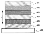
기판(400), 제1 전극(401), 제1 층(402), 제2 층(403), 제3 층(404), 제4 층(405) 및 제2 전극(406)이 동일한 재료로 그리고 실시예 모드 1의 방식과 동일한 방식으로 형성될 수 있기 때문에, 이러한 설명은 생략된다. 이러한 구조에서도, 제2 전극(406)의 전위보다 높은 전위를 제1 전극(401)에 공급함으로써 발광된다.The
더욱이, 도 4는 기판(400) 위에 형성된 제2 전극(406), 제2 전극(406) 위에 형성된 제4 층(405), 제4 층(405) 위에 형성된 제3 층(404), 제3 층(404) 위에 형성된 제2 층(403), 제2 층(403) 위에 형성된 발광 재료를 포함하는 제1 층(402) 및 제1 층(402) 위에 형성된 제1 전극(401)을 포함하는 구조를 가진다.Furthermore, FIG. 4 shows a
이러한 실시예에 기술된 구조에 있어서, 발광 재료를 포함하는 제1 층에서 캐리어들의 재결합에 의하여 생성된 광은 제1 전극(401)으로부터 외부로 방사된다.In the structure described in this embodiment, light generated by recombination of carriers in a first layer comprising a luminescent material is radiated outward from the
이러한 실시예에 기술된 이러한 구조에서조차, 실시예 1에 기술된 구조에 의하여 획득된 것과 동일한 장점이 획득될 수 있다. 특히, 제3 층과 제2 전극 사이에 제4 층이 설치되기 때문에, 자체 전위의 차이로 인한 전기 부식이 방지될 수 있다. 더욱이, 제3 층 및 제4 층의 막 두께가 자유롭게 세팅될 수 있기 때문에, 제1 층으로부터 반사 금속으로 형성된 제2 전극까지의 광학 길이는 더 용이하게 최적화될 수 있다. 더욱이, 제3 층으로부터 캐리어가 생성될 수 있기 때문에 전자들의 이동 거리는 종래의 구조를 가진 소자의 이동 거리보다 짧으며, 따라서 구동 전압이 감소될 수 있다. Even in this structure described in this embodiment, the same advantages as obtained by the structure described in Example 1 can be obtained. In particular, since the fourth layer is provided between the third layer and the second electrode, electrical corrosion due to the difference in its potential can be prevented. Moreover, since the film thicknesses of the third layer and the fourth layer can be freely set, the optical length from the first layer to the second electrode formed of the reflective metal can be more easily optimized. Moreover, since the carrier can be generated from the third layer, the moving distance of the electrons is shorter than the moving distance of the device having the conventional structure, and thus the driving voltage can be reduced.
[실시예 3][Example 3]
이러한 실시예는 도 5A 및 도 5B를 참조로 하여 화소부에서 본 발명에 따른 발광 소자를 가진 발광 장치를 설명한다. 도 5A는 발광 장치를 도시한 평면도이며, 도 5B는 도 5A의 A-A'를 따라 취한 단면도이다. 점선으로 도시된 도면부호 501은 구동 회로부(소스 구동 회로)를 도시하며, 도면부호 502는 화소부를 표시하며, 도면부호 503는 구동 회로부(게이트 구동 회로)를 표시하며, 도면부호 504는 밀봉 기판을 표시하며, 도면부호 505는 실란트를 표시하며, 도면부호 507은 실란트(505)에 의하여 둘러싸인 공간을 표시한다.This embodiment describes a light emitting device having a light emitting element according to the present invention in the pixel portion with reference to FIGS. 5A and 5B. 5A is a plan view of the light emitting device, and FIG. 5B is a cross-sectional view taken along the line AA ′ of FIG. 5A. 501 denotes a driving circuit portion (source driving circuit), 502 denotes a pixel portion, 503 denotes a driving circuit portion (gate driving circuit), and 504 denotes a sealing substrate.
리드 배선(lead wiring; 508)은 소스 구동 회로(501) 및 게이트 구동 회로(503)에 입력될 신호들을 전송하는 배선을 표시하며, 이는 외부 입력 단자로서 사용되는 FPC(가요성 인쇄 회로)로부터 비디오 신호, 클록 신호, 시작 신호 및 리셋 신호와 같은 신호들을 수신한다. FPC만이 본원에 기술될지라도, 인쇄 배선 기판(PWB)은 FPC에 부착될 수 있고 본 명세서의 발광 장치는 발광 장치 그 자체뿐만 아니라 FPC를 가진 발광 장치 또는 이에 부착된 PWB를 포함할 수 있다.Lead wiring 508 represents a wiring for transmitting signals to be input to the
다음으로, 단면 구조는 도 5B를 참조로 하여 설명된다. 구동 회로부 및 화소부는 기판(510) 위에 형성된다. 이러한 실시예에서는 구동 회로부인 소스 구동 회로(501) 및 화소부(502)가 도시된다.Next, the cross-sectional structure is described with reference to FIG. 5B. The driving circuit portion and the pixel portion are formed on the
소스 구동 회로(501)에는 n-채널 TFT 및 p-채널 TFT(524)이 결합된 CMOS 회로가 형성된다. 더욱이, 구동 회로를 형성하는 TFT는 알려져 있는 CMOS 회로, PMOS 회로 또는 NMOS 회로로 형성될 수 있다. 본 실시예가, 구동 회로가 동일한 기판 위에 형성되는 드라이버 일체형(driver integrated type)을 기술할지라도, 구동 회로는 기판 외부에 형성될 수 있다.In the
화소부(502)는 스위칭 TFT(511), 전류 제어 TFT(512) 및 전류 제어 TFT의 드레인과 전기적으로 접속된 제1 전극(513)을 포함하는 다수의 화소들로 형성된다. 절연체(514)는 제1 전극(513)의 단부를 덮도록 형성된다. 여기서, 양의 감광성 아크릴 수지막이 절연체(514)로서 사용된다.The
커버리지(coverage)를 개선하기 위하여, 절연체(514)는 상단부 또는 하단부에서 만곡부를 가지도록 형성된다. 예컨대, 절연체(514)에 대하여 양의 감광성 아크릴을 사용하는 경우에, 절연체(514)의 상단부만이 0.2㎛ 내지 3㎛의 만곡부의 반경을 가진다. 절연체(514)는 광의 조사에 의하여 에천트에 대하여 불용해성이 되는 네거티브 타입 또는 광의 조사에 의하여 에천트에 대하여 용해성이 되는 포지티브 타입 중 하나로 형성될 수 있다. 유기 화합물뿐만 아니라 산화규소 또는 산질화규소와 같은 무기 화합물이 사용될 수 있다. 더욱이, 적어도 수소를 포함하는 유기 그룹(알킬 그룹 또는 아릴 그룹과 같은), 플루오르 그룹 또는 적어도 수소를 포함하는 유기 그룹 및 플루오르 그룹, 소위 실록산을 치환기로서 가진 규소 및 산소의 결합에 의하여 형성된 골격 구조로 구성된 재료가 또한 사용될 수 있다.To improve coverage, the
제1 내지 제4 층들을 포함하는 전계 발광층(516) 및 제2 전극(517)은 제1 전극(513) 위에 각각 형성된다. 제1 전극(양극)(513)은 바람직하게 인듐 주석 산화물(ITO), 실리콘 산화물을 포함하는 인듐 주석 산화물(ITSO), 아연 산화물(ZnO), 2% 내지 20% 정도 아연 산화물을 포함하는 인듐 산화물(IZO), 갈륨을 포함하는 아연 산화물(GZO), 주석 산화물(SnO2) 또는 인듐 산화물(In2O3)과 같은 투광성 재료로 형성된다. The
전계 발광층(516)의 제1 내지 제4 층들은 저항 가열, 즉 증착 마스크 또는 잉크-젯법을 사용하는 전자 빔에 의한 증착법에 의하여 각각 형성된다. 전계 발광층(516)의 제1 내지 제4 층들은 발광 재료를 포함하는 제1 층, 제2 층, 투명 도전막을 포함하는 제3 층, 및 제4 층을 포함하며, 제1 층, 제2 층, 제3 층 및 제4 층은 제1 전극으로부터 제2 전극 쪽으로 순차적으로 적층되며, 제4 층은 제2 전극과 접하도록 형성된다. 발광 재료를 포함하는 층에 대한 재료로서, 유기 화합물은 일반적으로 단층, 다층 또는 혼합층 구조에 사용된다. 그러나, 본 발명에서는 무기 화합물이 유기 화합물을 포함하는 막의 일부로서 사용될 수 있다. 이러한 경우에, 스퍼터링법에 의하여 증착이 사용될 수 있다.The first to fourth layers of the
다수의 재료를 포함하는 층은 각각의 재료를 동시에 증착함으로써 형성될 수 있다. 다수의 재료를 포함하는 층은 저항 가열 증착법들을 사용하는 공증착법, 전자 빔 증착법들을 사용하는 공증착법, 저항 가열 증착법 및 전자 빔 증착법을 사용하는 공증착법, 저항 가열 증착법 및 스터터링법을 사용하는 증착법 또는 전자 빔 증착법 및 스퍼터링법을 사용하는 증착법과 같은 동일한 종류의 방법 또는 다른 종류의 방법들을 결합함으로써 형성된다. 더욱이, 두 가지 종류의 재료를 포함하는 층이 앞의 예들에서 가정될지라도, 다수의 재료를 포함하는 층은 3개 이상의 종류의 재료를 포함하는 경우에 유사하게 형성될 수 있다. Layers comprising multiple materials may be formed by depositing each material simultaneously. The layer comprising a plurality of materials may be co-deposited using resistive heat deposition, co-deposition using electron beam deposition, co-deposition using resistive heating and electron beam deposition, vapor deposition using resistive heating deposition and stuttering. Or by combining the same kind of methods or other kinds of methods such as the evaporation method using the electron beam deposition method and the sputtering method. Moreover, although a layer comprising two kinds of materials is assumed in the above examples, a layer comprising a plurality of materials may be similarly formed when including three or more kinds of materials.
고반사율을 가진 금속은 전계 발광층(516) 위에 형성된 제2 전극(517)(음극)에 대한 재료로서 바람직하다. 예컨대, 알루미늄(Al), 은(Ag), 또는 AlLi 합금 또는 MgAg 합금과 같이 Al 또는 Ag를 포함하는 합금이 사용될 수 있다. A metal having high reflectance is preferable as a material for the second electrode 517 (cathode) formed on the
게다가, 발광 소자(518)는 실란트(505)를 사용하여 소자 형성 기판(510)에 시일링 기판(504)을 부착함으로써 소자 형성 기판(510), 시일링 기판(504) 및 실란트(505)로 둘러싸인 공간(507) 내에 설치된다. 공간(507)은 충진 재료, 예컨대 질소 또는 아르곤과 같은 불활성 가스, 또는 실란트(505)로 충진된다.In addition, the
에폭시 기반 수지 등은 바람직하게 실란트(505)를 위하여 사용된다. 이들 재료들은 가능한 많이 산소 또는 수분을 전달하기 않는 것이 바람직하다. 시일링 기판(504)에 대한 재료로서, FRP(섬유유리-강화 플라스틱), PVF(폴리비닐 플루오르화물), 마일라(Mylar), 폴리에스터, 아크릴뿐만 아니라 유리 기판 또는 석영 기판이 사용될 수 있다.Epoxy-based resins and the like are preferably used for the
기술된 바와 같이, 본 발명에 따른 발광 소자를 가진 발광 장치가 획득될 수 있다.As described, a light emitting device having a light emitting element according to the present invention can be obtained.
이러한 실시예는 다른 실시예 모드 및 실시예들과 임의적으로 결합될 수 있다.Such an embodiment may be arbitrarily combined with other embodiment modes and embodiments.
[실시예 4]Example 4
본 실시예는 발광 재료를 포함하는 전술한 층의 구조를 상세히 설명한다.This embodiment describes in detail the structure of the above-described layer including the light emitting material.
발광 재료를 포함하는 층은 전하-주입-이송 재료 및 유기 화합물 또는 무기 화합물을 포함하는 발광 재료로 형성된다. 발광 재료를 포함하는 층은 저분자 중량 유기 화합물, 중간 분자 중량 유기 화합물 및 고분자 중량 유기 화합물로 이루어진 한 층 또는 다수의 층을 포함한다. 선택적으로, 전자-주입 이송 능력 또는 홀-주입 이송 능력을 가진 무기 화합물이 또한 결합될 수 있다. The layer comprising the luminescent material is formed of a luminescent material comprising a charge-injection-transport material and an organic compound or an inorganic compound. The layer comprising the luminescent material comprises one or more layers consisting of low molecular weight organic compounds, medium molecular weight organic compounds and high molecular weight organic compounds. Optionally, inorganic compounds having electron-injection transporting capability or hole-injection transporting capability may also be combined.
퀴놀라인 골격 또는 벤조퀴놀라인 골격을 가진 이하의 금속 착체 등은 전하-주입-이송 재료, 즉 트리(8-퀴놀리놀레이토)알루미늄(약어 Alq3), 트리(4-메틸-8-퀴놀리놀레이토)알루미늄(약어 Almq3), 비스(10-하이드록시벤조[h]-퀴놀리놀레이토)베릴륨(약어 BeBq2), 비스(2-메틸-8-퀴놀리놀레이토)-4-페닐페놀레이토-알루미늄(약어 BAlq) 등 중 고전자 이송 능력을 가진 재료의 예로서 주어질 수 있다. 더욱이, 방향족-아민 골격을 가진 이하의 재료(벤젠 링-질소 결합을 가진 재료)는 높은 홀 이송 능력을 가진 재료, 4,4'-비스[N-(1-나프틸)-N-페닐-아미노]-바이페닐 (약어 α-NPD), 4,4'-비스[N-(3-메틸페닐)-N-페닐-아미노]바이페닐 (약어 TPD), 4,4',4"-트리(N,N-디페닐-아미노)-트리페닐아민( 약어 TDATA), 4,4',4"-트리[N-(3-메틸페닐)-N-페닐-아미노]-트리페닐아민(약어 MTDATA) 등의 예로서 주어질 수 있다. The following metal complexes having a quinoline backbone or a benzoquinolone backbone are charge-injection-transfer materials such as tri (8-quinolinolato) aluminum (abbreviated Alq 3 ), tri (4-methyl-8- Quinolinolato) aluminum (abbreviated Almq 3 ), bis (10-hydroxybenzo [h] -quinolinolato) beryllium (abbreviated BeBq 2 ), bis (2-methyl-8-quinolinolato) -4 -Phenylphenolraito-aluminum (abbreviated BAlq) and the like can be given as an example of a material having a high electron transfer capacity. Furthermore, the following materials having an aromatic-amine backbone (materials having benzene ring-nitrogen bonds) are materials having high hole transport ability, 4,4'-bis [N- (1-naphthyl) -N-phenyl- Amino] -biphenyl (abbreviated α-NPD), 4,4'-bis [N- (3-methylphenyl) -N-phenyl-amino] biphenyl (abbreviated TPD), 4,4 ', 4 "-tri ( N, N-diphenyl-amino) -triphenylamine (abbreviated TDATA), 4,4 ', 4 "-tri [N- (3-methylphenyl) -N-phenyl-amino] -triphenylamine (abbreviated MTDATA) And the like.
더욱이, 리듐 플루오르화물(LiF), 세슘 플루오르화물(CsF) 또는 칼슘 플루오르화물(CaF2)와 같은 알칼리 금속 또는 알칼리 토금속의 화합물은 특히 전하-주입-이송 재료 중에서 높은 전자 주입 능력을 가진 재료의 예로서 주어질 수 있다. 부가적으로, Alq3와 같은 고전자 이송 능력 및 마그네슘(Mg)과 같은 알칼리 토금속의 혼합물이 공급될 수 있다.Moreover, compounds of alkali metals or alkaline earth metals such as lithium fluoride (LiF), cesium fluoride (CsF) or calcium fluoride (CaF 2 ) may be given as examples of materials with high electron injection capability, especially among charge-injection-transfer materials. have. In addition, a mixture of high electron transfer capacity such as Alq 3 and alkaline earth metal such as magnesium (Mg) may be supplied.
이하의 금속 산화물은 전하-주입-이송 재료, 즉 몰리브덴 산화물(MoOx), 바나듐 산화물(VOx), 루테늄 산화물(RuOx), 텅스텐 산화물(WOx), 망간 산화물(MnOx) 등 중에서 높은 홀 주입 능력을 가진 재료의 예로서 주어질 수 있다. 부가적으로, 프탈로시아닌(약어 H2Pc) 또는 구리 프탈로시아닌(CuPc)과 같은 프탈로사이닌 기반 화합물이 예로서 주어질 수 있다.The following metal oxides are higher among charge-injection-transfer materials, that is, molybdenum oxide (MoO x ), vanadium oxide (VO x ), ruthenium oxide (RuO x ), tungsten oxide (WO x ), manganese oxide (MnO x ), and the like. It can be given as an example of a material having a hole injection capability. In addition, phthalocyanine based compounds such as phthalocyanine (abbreviated H 2 Pc) or copper phthalocyanine (CuPc) may be given by way of example.
발광층은 각각의 화소에서 다른 방사 파장 범위들을 가진 발광층을 형성함으로써 색 표시를 수행하는 구조를 가질 수 있다. 전형적으로, R(적색), G(녹색) 및 B(청색)의 각각의 색에 대응하는 발광층이 형성된다. 이러한 경우에, 색순도가 개선될 수 있으며, 화소부의 미러(mirror) 표면은 화소로부터의 광이 방사되는 측면 상에 방사 파장 범위의 광이 전송되는 필터(칼라 층)를 가진 구조를 포함함으로써 방지될 수 있다. 필터(칼라 층)를 설치함으로써 통상적으로 필수적인 원평광판(circular polarizing plate) 등을 설치하는 것을 생략하는 것이 가능하며, 이는 발광층으로부터 방사된 광의 손실을 방지할 수 있다. 게다가, 화소부(표시 화면)를 비스듬하게 보는 경우에 생성되는 칼라 톤이 덜 변형될 수 있다.The light emitting layer may have a structure for performing color display by forming a light emitting layer having different emission wavelength ranges in each pixel. Typically, light emitting layers corresponding to the respective colors of R (red), G (green), and B (blue) are formed. In this case, color purity can be improved, and the mirror surface of the pixel portion can be prevented by including a structure having a filter (color layer) in which light in the emission wavelength range is transmitted on the side from which light from the pixel is emitted. Can be. By installing a filter (color layer), it is possible to omit the installation of a generally necessary circular polarizing plate or the like, which can prevent the loss of light emitted from the light emitting layer. In addition, the color tone generated when viewing the pixel portion (display screen) at an angle may be less deformed.
발광층을 형성하는 다양한 발광 재료들이 존재한다. 4-디시아노메틸렌-2-메틸-6-[2-(1,1,7,7-테트라메틸줄로리딘-9-일)에틴일]-4H-피란 (약어 DCJT), 4-디시아노메틸렌-2-t-부틸-6-[2-(1,1,7,7-테트라메틸줄로리딘-9-일)에틴일]-4H-피란, 페리플란덴, 2,5-디시아노-1,4-비스[2-(10-메톡시-1,1,7,7-테트라메틸줄로리딘-9-일)에틴일]벤젠,N,N'-디메틸퀴나크리돈 (약어 DMQd), 쿠마린6, 쿠마린545T, 트리(8-퀴놀리놀레이토)알루미늄 (약어 Alq3), 9,9'-바이드릴, 9,10-디페닐안드라센(약어 DPA), 9,10-비스(2-나프틸)안드라센(약어 DAN) 등은 저분자 중량 유기 발광 재료로서 사용될 수 있다. 선택적으로, 다른 재료가 또한 사용될 수 있다. There are various light emitting materials forming the light emitting layer. 4-dicyanomethylene-2-methyl-6- [2- (1,1,7,7-tetramethylzulolidin-9-yl) ethynyl] -4H-pyran (abbreviated DCJT), 4-dicyano Methylene-2-t-butyl-6- [2- (1,1,7,7-tetramethylzulolidin-9-yl) ethynyl] -4H-pyran, periflandene, 2,5-dicyano -1,4-bis [2- (10-methoxy-1,1,7,7-tetramethylzulolidin-9-yl) ethynyl] benzene, N, N'-dimethylquinacridone (abbreviated DMQd ), Coumarin 6, coumarin 545T, tri (8-quinolinolato) aluminum (abbreviated Alq 3 ), 9,9'-bidrill, 9,10-diphenylandracene (abbreviated DPA), 9,10-bis (2-naphthyl) andracene (abbreviated DAN) or the like can be used as the low molecular weight organic light emitting material. Optionally, other materials may also be used.
다른 한편으로, 고분자 중량 유기 발광 재료는 저분자 중량 유기 발광 재료와 비교하여 소자의 더 강한 물리적 강도 및 더 강한 내구성을 가진다. 더욱이, 코팅에 의한 막-형성이 가능하기 때문에, 소자의 제조가 더 용이하다. 고분자 중량 유기 발광 재료를 사용하는 발광 소자의 구조는 저분자 중량 유기 발광 재료의 사용하는 경우와 기본적으로 동일하며, 음극, 유기 발광층 및 양극은 적층된다. 그러나, 고분자 중량 유기 발광 재료를 사용하여 발광층을 사용할 때, 저분자 중량 유기 발광 재료를 사용하는 경우에서처럼 다층 구조를 형성하는 것이 곤란하며, 많은 경우에 두개의 층 구조가 형성된다. 특히, 음극, 발광층, 홀-이송층 및 양극은 다층 구조로 적층된다.On the other hand, high molecular weight organic light emitting materials have a stronger physical strength and stronger durability of the device compared to low molecular weight organic light emitting materials. Moreover, since film-forming by coating is possible, the fabrication of the device is easier. The structure of the light emitting device using the high molecular weight organic light emitting material is basically the same as the case of using the low molecular weight organic light emitting material, and the cathode, the organic light emitting layer, and the anode are laminated. However, when using a light emitting layer using a high molecular weight organic light emitting material, it is difficult to form a multilayer structure as in the case of using a low molecular weight organic light emitting material, and in many cases, two layer structures are formed. In particular, the cathode, the light emitting layer, the hole-transport layer and the anode are stacked in a multilayer structure.
발광 칼라가 발광층을 형성하는 재료들에 의존하기 때문에, 이들 재료들을 선택함으로써 적정 발광을 나타내는 발광 소자가 형성될 수 있다. 폴리파라페닐렌 비닐렌 기반, 폴리파라페닐렌 기반, 폴리디오펜 기반 및 폴리플루오르 기반 발광 재료들은 발광층을 형성하기 위하여 사용될 수 있는 고분자 중량 전계 발광 재료의 예로서 제공된다.Since the light emitting color depends on the materials forming the light emitting layer, by selecting these materials, a light emitting element exhibiting appropriate light emission can be formed. Polyparaphenylene vinylene based, polyparaphenylene based, polydiophene based and polyfluorine based luminescent materials are provided as examples of high molecular weight electroluminescent materials that can be used to form the light emitting layer.
폴리(파라페닐렌비닐렌)[PPV], 폴리(2,5-디올콕시-1,4-페닐렌비닐렌) [RO-PPV], 폴리(2-(2'-에틸-헥소시)-5-메톡시-1,4-페닐렌비닐렌) [MEH-PPV], 폴리(2-(디얼콕시페닐)-1,4-페닐렌비닐렌)[ROPh-PPV] 등의 유도체는 폴리파라페닐렌 비닐렌 기반 발광 재료의 예로서 주어질 수 있다. 폴리파라페닐렌[PPP], 폴리(2,5-디알콕시-1,4-페닐렌)[RO-PPP], 폴리(2,5-디헥소시-1,4-페닐렌) 등의 유도체가 폴리파라페닐렌 기반 발광 재료의 예로서 주어질 수 있다. 폴리디오펜[PT], 폴리(3-아킬디오펜)[PAT], 폴리(3-헥실디오펜)[PHT], 폴리(3-사이클로헥실디오펜)[PCHT], 폴리(3-사이클로헥실-4-메틸디오펜)[PCHMT], 폴리(3,4-디사이클로헥실디오펜)[PDCHT], 폴리[3-(4-옥틸페닐)-디오펜][POPT], 폴리[3-(4-옥틸페닐)-2,2바이디오펜][PTOPT] 등의 유도체가 폴리디오펜 기반 발광 재료의 예로서 주어질 수 있다. 폴리플루오렌[PF], 폴리(9,9-디알킬플루오렌)[PDAF], 폴리(9,9-다이옥틸플루오렌)[PDOF] 등의 유도체가 폴리플루오렌 기반 발광 재료의 예가 주어질 수 있다.
Poly (paraphenylenevinylene) [PPV], poly (2,5-dioloxy-1,4-phenylenevinylene) [RO-PPV], poly (2- (2'-ethyl-hexoxy) Derivatives such as -5-methoxy-1,4-phenylenevinylene) [MEH-PPV], poly (2- (dialkoxyphenyl) -1,4-phenylenevinylene) [ROPh-PPV] It can be given as an example of a polyparaphenylene vinylene based luminescent material. Derivatives such as polyparaphenylene [PPP], poly (2,5-dialkoxy-1,4-phenylene) [RO-PPP], poly (2,5-dihexoxy-1,4-phenylene) It can be given as an example of a polyparaphenylene based luminescent material. Polydiophene [PT], poly (3-acyldiophene) [PAT], poly (3-hexyldiophene) [PHT], poly (3-cyclohexyldiophene) [PCHT], poly (3-cyclohexyl-4-methyl Diophen) [PCHMT], poly (3,4-dicyclohexyldiophene) [PDCHT], poly [3- (4-octylphenyl) -diophene] [POPT], poly [3- (4-octylphenyl) -2 Derivatives such as, 2biophene] [PTOPT] can be given as examples of polydiophene based luminescent materials. Derivatives such as polyfluorene [PF], poly (9,9-dialkylfluorene) [PDAF], poly (9,9-dioctylfluorene) [PDOF] can be given as examples of polyfluorene-based light emitting materials. have.
*양극로부터의 홀 주입 능력은 홀 이송 능력을 가진 고분자 중량 유기 발광 재료가 양극과 발광 특성들을 가진 고분자 유기 발광 재료 사이에 끼워질 때 강화될 수 있다는 것에 유의해야 한다. 일반적으로, 고분자 중량 유기 발광 재료는 억셉터 재료(acceptor material)가 스핀-코팅법 등에 의하여 물에서 용해되는 용액으로 코팅된다. 더욱이, 억셉터 재료가 유기 용매에서 용해 불가능하기 때문에, 앞서 언급된 발광 특성들을 가진 유기 발광 재료는 적층될 수 있다. 억셉터 재료로서 PEDOT 및 캄포 술폰산(CSA)의 혼합물, 억셉터 재료로서 폴리아닐라인(PANI) 및 폴리스틸렌술포닉(PSS)의 혼합물 등은 홀 이송 능력을 가진 고분자 중량 유기 발광 재료의 예로서 주어질 수 있다.It should be noted that the hole injection capability from the anode can be enhanced when the high molecular weight organic light emitting material with hole transporting capacity is sandwiched between the anode and the high molecular weight organic light emitting material with luminescent properties. In general, high molecular weight organic light emitting materials are coated with a solution in which an acceptor material is dissolved in water by spin-coating or the like. Moreover, since the acceptor material is insoluble in the organic solvent, the organic light emitting material having the above-mentioned light emitting properties can be laminated. Mixtures of PEDOT and camphor sulfonic acid (CSA) as acceptor materials, mixtures of polyaniline (PANI) and polystyrenesulphonic (PSS) as acceptor materials, and the like can be given as examples of high molecular weight organic light emitting materials with hole transport capabilities. have.
더욱이, 발광층은 단색광 또는 백색광을 방사하는 구조를 가질 수 있다. 백색 발광 재료를 사용하는 경우는 화소로부터의 광이 방사되는 측면상에서 특정 파장을 가진 광을 방사하는 필터(칼라 층)를 가진 구조를 구성함으로써 칼라 표시를 가능하게 한다. Furthermore, the light emitting layer may have a structure for emitting monochromatic light or white light. When a white light emitting material is used, color display is made possible by constructing a structure having a filter (color layer) that emits light having a specific wavelength on the side from which light from the pixel is emitted.
백색광을 방사하는 발광층을 형성하기 위하여, 예컨대 Alq3, 적색 발광 안료인 나일 레드(Nile Red)로 부분적으로 도핑된 Alq3, Alq3, p-EtTAZ 및 TPD(방향족 디아민)은 백색광 방사를 획득할 수 있는 증착법에 의하여 순차적으로 적층된다. 더욱이, 스핀 코팅을 사용하는 코팅법에 의하여 EL을 형성하는 경우에, EL층은 바람직하게 코팅 후에 진공 가열에 의하여 소성(bake)된다. 예컨대, 전체 표면은 폴리(에틸렌디옥시디오펜)/폴리(스티렌술폰산) 용액(PEDOT/PSS)으로 코팅될 수 있으며 홀-주입층으로서 사용되는 막을 형성하도록 가열된다. 그 다음에, 전체 표면은 발광 중심 안료(1,1,4,4-테트라페닐-1,3-부타디엔(TPB), 4-디시아노메틸렌-2-메틸-6-(p-디메틸아미노-스티릴)-4H-피란(DCM1), 나일 레드 또는 쿠마린6)로 도핑된 폴리비닐 카르바졸(PVK) 용액으로 코팅될 수 있으며, 발광층으로서 사용되는 막을 형성하기 위하여 소성된다.To form a light emitting layer that emits white light, for example Alq 3 , Alq 3 , Alq 3 , p-EtTAZ and TPD (aromatic diamine) partially doped with a red luminescent pigment, Nile Red, can obtain white light emission. It is laminated sequentially by a vapor deposition method that can be. Moreover, in the case of forming the EL by a coating method using spin coating, the EL layer is preferably baked by vacuum heating after coating. For example, the entire surface may be coated with a poly (ethylenedioxydiophene) / poly (styrenesulfonic acid) solution (PEDOT / PSS) and heated to form a film used as a hole-injection layer. The entire surface was then subjected to luminescent center pigments (1,1,4,4-tetraphenyl-1,3-butadiene (TPB), 4-dicyanomethylene-2-methyl-6- (p-dimethylamino-sty) It may be coated with a polyvinyl carbazole (PVK) solution doped with reel) -4H-pyran (DCM1), nile red or coumarin 6) and fired to form a film used as a light emitting layer.
발광층은 단층으로 형성될 수 있으며, 전자 이송 능력을 가진 1,3,4-옥사디아졸 유도체(PBD)는 홀 이송 능력을 가진 폴리비닐 카르바졸(PVK)에 분산될 수 있다. 더욱이, 백색광 방사는 전자-이송제로서 30중량%의 PBD를 분산시키고 4가지 종류의 염료들(TPB, 쿠마린6, DCM1 및 나일 레드)의 적정 도즈들(doses)을 분산시킴으로써 획득될 수 있다. 여기에서 기술된 바와 같이 백색광 방사가 획득되는 발광 소자 외에, 적색광 방사, 녹색광 방사 또는 청색광 방사를 획득할 수 있는 발광 소자는 발광층의 재료들을 적절하게 선택함으로써 제조될 수 있다.The light emitting layer may be formed as a single layer, and 1,3,4-oxadiazole derivative (PBD) having an electron transport ability may be dispersed in polyvinyl carbazole (PVK) having a hole transport ability. Moreover, white light emission can be obtained by dispersing 30% by weight PBD as an electron-transporting agent and dispersing the appropriate doses of four types of dyes (TPB, coumarin 6, DCM1 and nile red). In addition to the light emitting element in which white light emission is obtained as described herein, a light emitting element capable of obtaining red light emission, green light emission or blue light emission can be manufactured by appropriately selecting materials of the light emitting layer.
게다가, 금속 착체 등을 포함하는 삼중항 여기 발광 재료는 단일항 여기 발광 재료 외에 발광층을 위하여 사용될 수 있다. 예컨대, 적색 발광 특성을 가진 화소, 녹색 발광 특성들을 가진 화소 및 청색 발광 특성을 가진 화소 중에서, 비교적 짧은 시간, 즉 절반으로 감소된 발광시간을 가진 적색 발광 특성들을 가진 화소는 삼중항 여기 발광 재료로 형성되며, 다른 화소들은 단일항 여기 발광 재료로 형성된다. 삼중항 여기 발광 재료가 바람직한 발광 효율을 가지기 때문에, 동일한 휘도를 얻는데 있어서 저전력 소비가 요구된다. 다시 말해서, 적색 화소에 삼중항 여기 발광 재료를 공급하는 경우에, 발광 소자로 흐른 소량의 전류량이 요구되며, 따라서 신뢰성이 강화될 수 있다. 적색 발광 특성들을 가진 화소 및 녹색 발광 특성들을 가진 화소는 삼중항 여기 발광 재료로 형성될 수 있으며, 청색 발광 특성들을 가진 화소는 전력 소비를 감소시키기 위하여 단일항 여기 발광 재료로 형성될 수 있다. 게다가, 삼중항 여기 발광 재료로부터 인간의 높은 스펙트럴 발광 효율을 가진 녹색 발광 소자를 형성함으로써 저전력 소비가 실현될 수 있다. In addition, triplet excitation light emitting materials including metal complexes and the like can be used for the light emitting layer in addition to singlet excitation light emitting materials. For example, among pixels having red light emitting characteristics, pixels having green light emitting characteristics, and pixels having blue light emitting characteristics, pixels having red light emitting characteristics having a relatively short time, that is, a light emission time reduced by half, may be a triplet excitation light emitting material. And other pixels are formed of a singlet excitation light emitting material. Since the triplet excited light emitting material has a preferable luminous efficiency, low power consumption is required to obtain the same brightness. In other words, in the case of supplying the triplet excitation light emitting material to the red pixel, a small amount of current flowing to the light emitting element is required, and thus reliability can be enhanced. A pixel having red emission characteristics and a pixel having green emission characteristics may be formed of a triplet excitation light emitting material, and a pixel having blue emission characteristics may be formed of a singlet excitation light emitting material in order to reduce power consumption. In addition, low power consumption can be realized by forming a green light emitting device having a high spectral luminous efficiency of human from triplet excited light emitting material.
도펀트로서 사용된 금속 착체, 제3 전이 계열 원소인 백금이 중심 금속으로서 사용되는 금속 착체, 이리듐이 중심 금속으로서 사용되는 금속 착체 등은 삼중항 여기 발광 재료의 예로서 알려져 있다. 삼중항 여기 발광 재료는 이들 화합물들에 제한되지 않으며, 중심 금속에 대하여 주기율표의 8 내지 10족에 속하는 원소를 갖고 앞의 구조를 가진 화합물을 사용하는 것이 가능하다.Metal complexes used as dopants, metal complexes in which platinum as the third transition series element is used as the center metal, metal complexes in which iridium is used as the center metal, and the like are known as examples of triplet excitation light emitting materials. The triplet excitation light emitting material is not limited to these compounds, and it is possible to use a compound having an element belonging to
발광층을 형성하는 전술한 재료들은 예로서 기술되며, 발광 소자는 홀-주입-이송층, 홀-이송층, 전자-주입-이송층, 전자-이송층, 발광층, 전자-차단층, 또는 홀-차단층과 같은 각각의 기능층을 적절하게 적층시킴으로써 형성될 수 있다. 더욱이, 혼합층 또는 이들 층들의 각각이 혼합되는 혼합 접합이 형성될 수 있다. 발광층의 층 구조는 변경가능할 수 있다. 특정 전자-주입 영역 및 발광 영역 대신에 전자 주입을 위한 전극을 설치하고 발광 재료를 분사시켜 제공하는 수정들이 본 발명의 범위 내에서 허용가능하다.The above-mentioned materials for forming the light emitting layer are described by way of example, and the light emitting element may be a hole-injection-transport layer, a hole-transport layer, an electron-injection-transport layer, an electron-transport layer, an emission layer, an electron-blocking layer, or a hole- It can be formed by appropriately stacking each functional layer, such as a blocking layer. Furthermore, a mixed layer or a mixed junction in which each of these layers are mixed can be formed. The layer structure of the light emitting layer may be changeable. Modifications which provide an electrode for electron injection instead of a specific electron-injection region and a light emitting region and inject by providing a light emitting material are acceptable within the scope of the present invention.
앞서 언급된 재료를 사용하여 형성된 발광 소자는 순방향으로 바이어싱됨으로써 발광한다. 발광 소자를 사용하여 형성된 표시 장치의 화소는 단순한 매트릭스 모드 또는 능동 매트릭스 모드에 의하여 구동될 수 있다. 임의의 경우에, 각각의 화소는 특정 시간에 그에 순방향 바이어스를 공급하여 방사되나, 화소는 임의의 주기 동안 비발광 상태를 유지한다. 발광 소자의 신뢰성은 발광 주기 동안 반대 방향으로 바이어스(역바이어스)를 공급함으로써 강화될 수 있다. 발광 소자에서, 임의의 구동 조건하에서 방사 강도가 감소되는 열화 모드 또는 화소의 비발광 영역의 확장으로 인하여 휘도가 명백하게 감소되는 열화 모드가 존재한다. 그러나, 열화의 진행은 교류 전류 구동에 의하여 지연될 수 있다. 따라서, 발광 장치의 신뢰성이 강화될 수 있다.The light emitting element formed using the aforementioned material emits light by biasing in the forward direction. The pixel of the display device formed using the light emitting element can be driven by a simple matrix mode or an active matrix mode. In any case, each pixel is radiated by supplying a forward bias to it at a particular time, but the pixel remains non-luminescing for any period. The reliability of the light emitting element can be enhanced by supplying a bias (reverse bias) in the opposite direction during the light emitting period. In the light emitting element, there is a degradation mode in which the emission intensity is reduced under certain driving conditions or a degradation mode in which the luminance is obviously reduced due to the expansion of the non-emitting region of the pixel. However, the progress of deterioration can be delayed by the AC current driving. Therefore, the reliability of the light emitting device can be enhanced.
이러한 실시예는 다른 실시예 모드 및 실시예들과 임의적으로 결합될 수 있다.Such an embodiment may be arbitrarily combined with other embodiment modes and embodiments.
[실시예 5][Example 5]
본 실시예는 실시예 3에 기술된 발광 장치가 설치된 모듈을 설명한다.This embodiment describes a module in which the light emitting device described in
도 7A에 도시된 정보 단말의 모듈(999)에서, 제어기(901), 중앙처리장치(CPU)(902), 메모리(911), 전원회로(903), 오디오 처리 회로(929), 및 송신기/수신기 회로(904)뿐만 아니라 저항기, 버퍼 및 용량 소자와 같은 다른 소자들은 인쇄 배선 기판(946) 상에 장착된다. 더욱이, 발광 장치를 포함하는 표시 패널(900)은 가요성 인쇄 회로(FPC)(908)를 통해 인쇄 배선 기판(946)에 접속된다.In
표시 패널(900)은 발광 소자가 각각의 화소에 배치된 화소부(905), 화소부(905)에 포함된 화소를 각각 선택하는 제1 주사선 구동 회로(906a) 및 제2 주사선 구동 회로(906b), 및 선택된 화소에 비디오 신호를 공급하는 신호선 구동 회로(907)를 포함한다. The
다양한 제어 신호들은 인쇄 배선 기판(946)을 위하여 설치된 인터페이스(I/F)부(909)를 통해 입력 및 출력된다. 더욱이, 인쇄 배선 기판(946)에는 안테나로/안테나로부터 신호들을 전송/수신하는 안테나 포트(910)가 설치된다.Various control signals are input and output through an interface (I / F)
비록 인쇄 배선 기판(946)이 본 실시예에서 FPC(908)를 통해 표시 패널(900)에 접속될지라도, 본 발명은 본 구조에 반드시 제한되지 않는다. 제어기(901), 오디오 처리 회로(929), 메모리(911), CPU(902), 또는 전원 회로(903)는 COG(유리 상 칩)법에 의하여 표시 패널(900) 상에 직접 장착될 수 있다. 더욱이, 인쇄 배선 기판(946)에는 전원 전압 또는 신호들에 잡음이 발생하는 것 또는 신호의 상승이 저속으로 되는 것을 방지하는 용량 소자 또는 버퍼와 같은 다양한 소자들이 설치된다. Although the printed
도 7B는 도 7A에 도시된 모듈(999)의 블록도를 도시한다. 이러한 모듈(999)은 메모리(911)로서 VRAM(932), DRAM(925), 플래시 메모리(926) 등을 포함한다. 패널에 표시될 이미지의 데이터는 VRAM(932)에 저장되며, 이미지 데이터 또는 오디오 데이터는 DRAM(925)에 저장되며, 다양한 프로그램들이 플래시 메모리(926)에 저장된다.FIG. 7B shows a block diagram of the
전원 회로(903)에서는 표시 패널(900), 제어기(901), CPU(902), 오디오 처리 회로(929), 메모리(911) 및 송신기/수신기 회로(931)에 대한 전력 공급 전압이 생성된다. 임의의 경우에, 전원 회로(903)는 패널 사양에 따라 전류원이 제공된다.In the
CPU(902)는 제어 신호 생성 회로(920), 디코더(921), 레지스터(922), 동작 회로(923), RAM(924), CPU에 대한 인터페이스(935) 등을 포함한다. 인터페이스(935)를 통해 CPU(902)에 입력되는 다양한 신호들은 일단 레지스터(922)에 저장되며, 그 다음에 동작 회로(923), 디코더(921) 등에 입력된다. 동작 회로(923)에서는 입력된 신호에 기초하여 동작이 수행되며 다양한 명령들이 전송되는 위치가 지정된다. 다른 한편으로, 디코더(921)에 입력된 신호는 디코딩된 후 제어 신호 생성 회로(920)에 입력된다. 다양한 명령들을 포함하는 신호는 입력된 신호에 기초하여 제어 신호 생성 회로(920)에서 생성되며, 동작 회로(923)에 의하여 지정된 위치, 특히 메모리(911), 송신기/수신기 회로(931), 오디오 처리 회로(929), 제어기 등에 전송된다.The
메모리(911), 송신기/수신기 회로(931), 오디오 처리 회로(929) 및 제어기(901)는 수신된 명령들의 각각에 따라 각각 동작한다. 각각의 동작은 이후에 간략하게 설명된다.The
입력 수단(933)으로서 입력된 신호는 인터페이스(909)를 통해 인쇄 배선 기판(946) 상에 장착된 CPU(902)에 전송된다. 제어 신호 생성 회로(920)에서, VRAM(932)에 저장된 이미지 데이터는 포인팅 장치 또는 키보드와 같은 입력 수단(933)으로부터 전송된 신호에 따라 미리 결정된 포맷으로 변환되며 제어기(901)에 전송된다.The signal input as the input means 933 is transmitted to the
CPU(902)로부터 전송된 이미지 데이터를 포함하는 신호는 제어기(901)의 패널 사양에 따라 처리된 데이터이며 표시 패널(900)에 공급된다. 더욱이, 수평 동기(Hsync) 신호, 수직 동기(Vsync) 신호, 클록 신호(CLK), 교류 전압(AC Cont) 및 스위칭-오버 신호(L/R)는 전원 회로(903)로부터 입력된 전원 전압 또는 CPU(902)로부터 입력된 다양한 신호들에 따라 제어기(901)에서 생성되어, 표시 패널(900)에 공급된다. The signal including the image data transmitted from the
송신기/수신기 회로(904)에서는 안테나(934)에서 전파로서 전송 및 수신되는 신호가 처리되며, 특히 절연체, 대역 통과 필터, VCO(전압 제어 발진기), LPF(저역통과 필터), 결합기(coupler) 또는 발룬(balun)과 같은 고주파 회로가 포함된다. 송신기/수신기 회로(904)에서 전송 및 수신된 신호들 중 오디오 정보를 포함하는 신호는 CPU(902)의 명령에 의하여 오디오 처리 회로(929)에 전송된다.Transmitter /
CPU(902)의 명령에 의하여 전송된 오디오 정보를 포함하는 신호는 오디오 처리 회로(929)에서 오디오 신호로 복조되며, 스피커(928)에 전송된다. 마이크로폰(927)으로부터 전송된 오디오 신호는 오디오 처리 회로(929)에서 변조되며, CPU(902)의 명령에 의하여 송신기/수신기 회로(904)에 전송된다.The signal including the audio information transmitted by the command of the
제어기(901), CPU(902), 전원 회로(903), 오디오 처리 회로(929) 및 메모리(911)는 본 실시예의 패키지로서 장착될 수 있다. 이러한 실시예는 절연체, 대역 통과 필터, VCO(전압 제어 발진기), LPF(저역 통과 필터), 결합기 또는 바룬과 같은 고주파 회로에 적용될 수 있다.The
표시 패널(900)에서는 투명 도전막이 발광 소자의 광학 길이를 최적화하면서 반사 전극과 직접 접하지 않는다. 따라서, 투명 도전막 및 반사 전극의 전기 부식이 방지될 수 있다. 따라서, 이러한 표시 패널(900)을 갖춘 모듈(999)에서, 전기 부식에 의한 열화가 감소될 수 있으며, 표시 품질이 개선된다. 따라서, 우수한 표시 품질, 고신뢰성 및 긴 수명을 가진 모듈을 제공하는 것이 가능하다.In the
이러한 실시예는 다른 실시예 모드 및 실시예들과 임의적으로 결합될 수 있다.Such an embodiment may be arbitrarily combined with other embodiment modes and embodiments.
[실시예 6][Example 6]
도 8은 실시예 5에 기술된 바와 같이 모듈(999)을 포함하는 전자 장치의 하나의 모드를 도시한다. 표시 패널(900)은 자유 탈착 방식으로 하우징(1001)에 통합됨으로써 모듈(999)과 용이하게 일체형으로 될 수 있다. 하우징(1001)의 형상 또는 크기는 하우징(1001)이 통합되는 전자 장치에 따라 임의적으로 변경될 수 있다.FIG. 8 illustrates one mode of an electronic device including the
표시 패널(900)을 고정하는 하우징(1001)은 인쇄 배선 기판(946)에 삽입되고 모듈로서 설치된다. 제어기, CPU, 메모리, 및 전원 회로뿐만 아니라 저항기, 버퍼 및 용량 소자와 같은 다른 소자들은 인쇄 배선 기판(946) 상에 장착된다. 게다가, 오디오 처리 회로, 송신기/수신기 회로 등은 목적에 따라 장착될 수 있다. 표시 패널(900)은 FPC(908)을 통해 인쇄 배선 기판(946)에 접속된다.The
이러한 모듈(999), 입력 수단(998), 및 배터리(997)는 케이싱들(casings; 996) 내에서 유지된다. 표시 패널(900)의 화소부는 케이싱(996) 내에 형성된 개구창(opening window)으로부터 보일 수 있도록 배치된다.This
표시 패널(900)에서는 투명 도전막이 발광 소자의 광학 길이를 최적화시키면서 반사 전극과 직접 접하지 않는다. 따라서, 투명 도전막 및 반사 전극의 전기 부식이 방지될 수 있다. 따라서, 이러한 표시 패널(900)을 갖춘 모듈(999)에서, 전기 부식에 의한 열화는 감소될 수 있으며 표시 품질은 개선된다. 따라서, 우수한 표시 품질, 고신뢰성 및 긴 수명을 가진 셀룰라 전화를 제공하는 것이 가능하다.
In the
*[실시예 7]* [Example 7]
본 실시예는 실시예 5에 기술된 모듈이 장착되고 실시예 6에 기술된 장치와 다른 전자 장치의 모드를 설명한다.This embodiment describes a mode of an electronic device that is different from the device described in Embodiment 6, in which the module described in
본 발명에 따른 발광 소자들을 가진 발광 장치들을 사용하여 제조된 전자 장치들은 비디오 카메라 또는 디지털 카메라와 같은 카메라, 고글형 디스플레이(헤드 장착 디스플레이), 네비게이션 시스템, 오디오 재생 장치(카 오디오 또는 오디오 컴포넌트), 퍼스널 컴퓨터, 게임기, 휴대용 정보 단말(모바일 컴퓨터, 셀룰라 전화, 휴대용 게임기, 전자책 등), 기록 매체를 가진 이미지 재생 장치(특히, DVD와 같은 기록 매체를 재생할 수 있고 이미지를 표시할 수 있는 표시 장치를 가진 장치) 등을 포함한다. 이들 전자 장치들은 도 6A 내지 도 6E에 상세히 도시되어 있다.Electronic devices manufactured using light emitting devices with light emitting elements according to the present invention include cameras such as video cameras or digital cameras, goggle displays (head mounted displays), navigation systems, audio playback devices (car audio or audio components), Image playback devices having personal computers, game consoles, portable information terminals (mobile computers, cell phones, portable game consoles, e-books, etc.) and recording media (especially display devices capable of playing back and displaying images such as DVDs) Device having a) and the like. These electronic devices are shown in detail in FIGS. 6A-6E.
도 6A는 케이싱(9101), 지지대(9102), 표시부(9103), 스피커부들(9104), 비디오 입력 단말(9105) 등을 포함하는 텔레비전 수신기이다. 텔레비전 수신기는 표시부(9103)와 관련하여 본 발명의 발광 소자를 가진 발광 장치를 사용함으로써 제조된다. 반사 금속과 투명 도전막은 표시부(9103)의 발광 소자의 광학 길이를 최적화하면서 집적 접하지 않는다. 따라서, 자체 전위들의 차이로 인한 전기 부식은 방지될 수 있으며, 따라서 텔레비전 수신기의 신뢰성이 개선된다. 텔레비전 수신기는 컴퓨터, TV 방송 수신, 광고 표시 등에 대한 모든 정보 표시 장치를 포함한다는 것에 유의해야 한다.6A is a television receiver including a
도 6B는 본체(9201), 케이싱(9202), 표시부(9203), 키보드(9204), 외부 접속 포트(9205), 포인팅 마우스(9206) 등을 포함하는 퍼스널 컴퓨터이다. 퍼스널 컴퓨터는 표시부(9203)와 관련하여 본 발명의 발광 소자를 가진 발광 장치를 사용함으로써 제조된다. 반사 금속과 투명 도전막은 표시부(9203)의 발광 소자의 광학 길이를 최적화하면서 집적 접하지 않는다. 따라서, 자체 전위들의 차이로 인한 전기 부식은 방지될 수 있으며, 따라서 퍼스널 컴퓨터의 신뢰성이 개선된다. FIG. 6B is a personal computer including a
도 6C는 본체(9301), 표시부(9302), 암부들(9303) 등을 포함하는 고글형 디스플레이이다. 고글형 디스플레이는 표시부(9302)와 관련하여 본 발명의 발광 소자를 가진 발광 장치를 사용함으로써 제조된다. 반사 금속과 투명 도전막은 표시부(9302)의 발광 소자의 광학 길이를 최적화하면서 집적 접하지 않는다. 따라서, 자체 전위들의 차이로 인한 전기 부식이 방지될 수 있으며, 따라서 고글형 디스플레이의 신뢰성이 개선된다. 6C is a goggle display including a
도 6D는 본체(9401), 케이싱(9402), 표시부(9403), 오디오 입력부(9404), 오디오 출력부(9405), 조작키들(9406), 외부 접속 포트(9407), 안테나(9408) 등을 포함하는 셀룰라 전화이다. 셀룰라 전화는 표시부(9403)와 관련하여 본 발명의 발광 소자를 가진 발광 장치를 사용함으로써 제조된다. 반사 금속과 투명 도전막은 표시부(9403)의 발광 소자의 광학 길이를 최적화하면서 집적 접하지 않는다. 따라서, 자체 전위들의 차이로 인한 전기 부식이 방지될 수 있으며, 따라서 셀룰라 전화의 신뢰성이 개선된다. 셀룰라 전화의 전력 소비는 표시부(9403)의 검은색 배경 상에 흰색 문자들을 표시함으로써 억제될 수 있다는 것에 유의해야 한다.6D shows a
도 6E는 본체(9501), 표시부(9502), 케이싱(9503), 외부 접속 포트(9504), 원격 제어 수신부(9505), 이미지 수신부(9506), 배터리(9507), 오디오 입력부(9508), 조작키들(9509), 접안부(9510) 등을 포함하는 비디오 카메라이다. 비디오 카메라는 표시부(9502)와 관련하여 본 발명의 발광 소자를 가진 발광 장치를 사용함으로써 제조된다. 반사 금속 및 투명 도전막은 표시부(9502)의 발광 소자의 광학 길이를 최적화하면서 집적 접하지 않는다. 따라서, 자체 전위들의 차이로 인한 전기 부식이 방지될 수 있으며, 따라서 비디오 카메라의 신뢰성이 개선된다.6E shows a
앞서 언급된 바와 같이, 본 발명에 따른 발광 소자를 가진 발광 장치는 넓은 범위에 걸쳐 적용될 수 있으며, 이러한 발광 장치는 모든 분야의 전자 장치들에 적용될 수 있다. 본 발명의 발광 소자를 사용함으로써, 발광 재료를 포함하는 층으로부터 반사 금속까지의 광학 길이는 구동 전압을 증가시키지 않고 최적화될 수 있다.As mentioned above, the light emitting device having the light emitting element according to the present invention can be applied over a wide range, and the light emitting device can be applied to electronic devices in all fields. By using the light emitting element of the present invention, the optical length from the layer containing the luminescent material to the reflective metal can be optimized without increasing the driving voltage.
이러한 실시예는 다른 실시예 모드 및 실시예들과 임의적으로 결합될 수 있다.Such an embodiment may be arbitrarily combined with other embodiment modes and embodiments.
[실시예 8][Example 8]
도 9 내지 도 12는 본 발명의 발광 소자의 특징들을 그래프로 각각 도시한다. 도 9는 전류 밀도-휘도 특징을 도시하며, 도 10은 전압-휘도 특징을 도시하며, 도 11은 휘도-전류 효율 특징을 도시하며, 도 12는 방사 스펙트럼을 도시한다.9 to 12 show graphically the features of the light emitting device of the invention, respectively. 9 shows the current density-luminance feature, FIG. 10 shows the voltage-luminance feature, FIG. 11 shows the luminance-current efficiency feature, and FIG. 12 shows the emission spectrum.
발광 소자는 유리 기판 위에 형성되며, 순차적으로 ITO는 제1 전극(101)으로서 110nm 두께로 유리 기판으로부터 형성된다. ITO는 스퍼터링법에 의하여 형성되고 2nm×2nm 크기의 형상을 가지도록 에칭된다. 다음으로, 기판의 표면은 다공성 수지(전형적으로, PVA(폴리비닐 알코올), 나일론 등으로 형성됨)로 세척되며, 열 처리는 한시간 동안 200℃에서 수행되며, UV 오존 처리는 제1 전극(101) 위에 발광 소자를 형성하기 위한 전처리로서 370초 동안 수행된다.The light emitting element is formed on the glass substrate, and in turn, ITO is formed from the glass substrate with a thickness of 110 nm as the
그 다음에, CuPc는 홀-주입층이 20nm 두께를 가지도록 형성된다. 다음으로, NPB는 홀-이송층으로서 40nm 두께를 가지도록 형성된다. Alq3 및 쿠마린6은 발광층이 1:0.01의 질량비를 가지도록 적층막들 위에 형성된다. 발광층은 40nm 두께를 가지도록 형성된다. 이러한 실시예에 있어서, 홀-주입층, 홀-이송층 및 발광층의 3개의 층은 제1 층(102)에 대응한다. 게다가, Alq3 및 리듐은 제2 층(103)으로서 1:0.01의 질량비를 가지도록 형성된다. 제2 층은 30nm 두께를 가지도록 형성된다. 그 다음에, 몰리브덴 산화물은 제3 층(104)으로서 110nm 두께를 가지도록 형성되며, NPB 및 몰리브덴 산화물은 제4 층(104)으로서 1:0.25의 질량비를 가지도록 형성된다. 제4 층(105)이 140nm 두께를 가지도록 형성된다는 것에 유의해야 한다. 다음에, Al은 200nm 두께의 제2 전극(106)으로서 소자들을 완성하도록 형성되며, 마지막 시일링은 소자들이 대기에 노출되지 않도록 질소 대기하에서 수행된다. 제2 전극에 대한 홀-주입층의 막 형성들 중 어느 하나는 저항 가열에 의한 진공 증기 증착법에 의하여 수행된다는 것에 유의해야 한다.Next, CuPc is formed such that the hole-injection layer has a thickness of 20 nm. Next, the NPB is formed to have a thickness of 40 nm as a hole-transport layer. Alq 3 and coumarin 6 are formed on the laminated films so that the light emitting layer has a mass ratio of 1: 0.01. The light emitting layer is formed to have a thickness of 40nm. In this embodiment, three layers of the hole-injection layer, the hole-transport layer and the light emitting layer correspond to the
도 9 내지 도 11은 본 발명의 발광 소자가 발광 소자로서 양호하게 기능을 한다는 것을 도시한다. 더욱이, 도 12는 본 실시예의 발광 소자가 양호한 녹색광을 방사한다는 것을 도시한다.9 to 11 show that the light emitting element of the present invention functions well as a light emitting element. Moreover, Fig. 12 shows that the light emitting element of this embodiment emits good green light.
101: 제1 전극
102: 제1 층
103: 제2 층
104: 제3 층
105: 제4 층
106: 제2 전극101: first electrode
102: first layer
103: second layer
104: the third layer
105: fourth layer
106: second electrode
Claims (29)
상기 양극 위에 형성되고 발광 재료를 포함하는 제1 층;
상기 제1 층 위에 형성되고 상기 제1 층과 직접 접하는 제2 층;
상기 제2 층 위에 형성되고 상기 제2 층과 직접 접하고 투명 도전막을 포함하는 제3 층;
상기 제3 층 위에 형성되고 제1 홀-이송 재료를 포함하는 제4 층; 및
상기 제4 층 위에 형성되고 상기 제4 층과 직접 접하고 금속을 포함하는 음극을 포함하고,
상기 제2 층은 아연 산화물, 주석 산화물, 티타늄 산화물, 아연 황화물, 아연 셀렌화물, 및 아연 텔루르화물로부터 선택된 재료를 포함하고,
상기 투명 도전막은 주석 산화물, 인듐 산화물, 아연 산화물, 갈륨을 포함하는 아연 산화물, 및 몰리브덴 산화물로 구성된 그룹으로부터 선택된 재료를 포함하는, 발광 장치.anode;
A first layer formed over said anode and comprising a luminescent material;
A second layer formed over the first layer and in direct contact with the first layer;
A third layer formed on the second layer and in direct contact with the second layer and including a transparent conductive film;
A fourth layer formed over the third layer and comprising a first hole-transport material; And
A cathode formed over the fourth layer and in direct contact with the fourth layer and comprising a metal,
The second layer comprises a material selected from zinc oxide, tin oxide, titanium oxide, zinc sulfide, zinc selenide, and zinc telluride,
And the transparent conductive film comprises a material selected from the group consisting of tin oxide, indium oxide, zinc oxide, zinc oxide, and molybdenum oxide.
상기 제1 홀-이송 재료는 유기 화합물인, 발광 장치.The method of claim 1,
Wherein the first hole-transport material is an organic compound.
상기 유기 화합물은 방향족-아민 골격(aromatic-amine skeleton)을 가진 재료인, 발광 장치.The method of claim 2,
Wherein said organic compound is a material having an aromatic-amine skeleton.
상기 양극과 상기 제1 층 사이에 제5 층을 더 포함하는, 발광 장치.The method of claim 1,
And a fifth layer between the anode and the first layer.
상기 제5 층은 제2 홀-이송 재료를 포함하는, 발광 장치.The method of claim 4, wherein
And the fifth layer comprises a second hole-transport material.
상기 양극 위에 형성되고 발광 재료를 포함하는 제1 층;
상기 제1 층 위에 형성되고 상기 제1 층과 직접 접하는 제2 층;
상기 제2 층 위에 형성되고 상기 제2 층과 직접 접하고 투명 도전막을 포함하는 제3 층;
상기 제3 층 위에 형성되고 유기 화합물에 전자-수용 재료가 도핑된 재료를 포함하는 제4 층; 및
상기 제4 층 위에 형성되고 상기 제4 층과 직접 접하고 금속을 포함하는 음극을 포함하고,
상기 제2 층은 아연 산화물, 주석 산화물, 티타늄 산화물, 아연 황화물, 아연 셀렌화물, 및 아연 텔루르화물로부터 선택된 재료를 포함하고,
상기 투명 도전막은 주석 산화물, 인듐 산화물, 아연 산화물, 갈륨을 포함하는 아연 산화물, 및 몰리브덴 산화물로 구성된 그룹으로부터 선택된 재료를 포함하는, 발광 장치.anode;
A first layer formed over said anode and comprising a luminescent material;
A second layer formed over the first layer and in direct contact with the first layer;
A third layer formed on the second layer and in direct contact with the second layer and including a transparent conductive film;
A fourth layer formed over said third layer and comprising a material doped with an electron-accepting material in an organic compound; And
A cathode formed over the fourth layer and in direct contact with the fourth layer and comprising a metal,
The second layer comprises a material selected from zinc oxide, tin oxide, titanium oxide, zinc sulfide, zinc selenide, and zinc telluride,
And the transparent conductive film comprises a material selected from the group consisting of tin oxide, indium oxide, zinc oxide, zinc oxide, and molybdenum oxide.
상기 유기 화합물은 홀-이송 재료인, 발광 장치.The method according to claim 6,
Wherein said organic compound is a hole-transport material.
상기 양극과 상기 제1 층 사이에 제5 층을 더 포함하는, 발광 장치.The method according to claim 6,
And a fifth layer between the anode and the first layer.
상기 제5 층은 홀-이송 재료를 포함하는, 발광 장치.The method of claim 8,
And the fifth layer comprises a hole-transport material.
상기 양극 위에 형성되고 발광 재료를 포함하는 제1 층;
상기 제1 층 위에 형성되고 상기 제1 층과 직접 접하고 제1 유기 화합물에 전자-공급 재료가 도핑된 재료를 포함하는 제2 층;
상기 제2 층 위에 형성되고 상기 제2 층과 직접 접하고 투명 도전막을 포함하는 제3 층;
상기 제3 층 위에 형성되고 제1 홀-이송 재료를 포함하는 제4 층; 및
상기 제4 층 위에 형성되고 상기 제4 층과 직접 접하고 금속을 포함하는 음극을 포함하고,
상기 투명 도전막은 주석 산화물, 인듐 산화물, 아연 산화물, 갈륨을 포함하는 아연 산화물, 및 몰리브덴 산화물로 구성된 그룹으로부터 선택된 재료를 포함하는, 발광 장치.anode;
A first layer formed over said anode and comprising a luminescent material;
A second layer formed over said first layer and comprising a material in direct contact with said first layer and doped with an electron-supply material in said first organic compound;
A third layer formed on the second layer and in direct contact with the second layer and including a transparent conductive film;
A fourth layer formed over the third layer and comprising a first hole-transport material; And
A cathode formed over the fourth layer and in direct contact with the fourth layer and comprising a metal,
And the transparent conductive film comprises a material selected from the group consisting of tin oxide, indium oxide, zinc oxide, zinc oxide, and molybdenum oxide.
상기 제1 홀-이송 재료는 제2 유기 화합물인, 발광 장치.11. The method of claim 10,
Wherein the first hole-transport material is a second organic compound.
상기 제2 유기 화합물은 방향족-아민 골격을 가진 재료인, 발광 장치.The method of claim 11,
And said second organic compound is a material having an aromatic-amine skeleton.
상기 제1 홀-이송 재료는 무기 화합물인, 발광 장치.11. The method according to claim 1 or 10,
Wherein the first hole-transport material is an inorganic compound.
상기 무기 화합물은 바나듐 산화물, 크롬 산화물, 몰리브덴 산화물, 코발트 산화물, 및 니켈 산화물로부터 선택되는, 발광 장치.The method of claim 13,
Wherein said inorganic compound is selected from vanadium oxide, chromium oxide, molybdenum oxide, cobalt oxide, and nickel oxide.
상기 양극과 상기 제1 층 사이에 제5 층을 더 포함하는, 발광 장치.11. The method of claim 10,
And a fifth layer between the anode and the first layer.
상기 제5 층은 제2 홀-이송 재료를 포함하는, 발광 장치.The method of claim 15,
And the fifth layer comprises a second hole-transport material.
상기 양극 위에 형성되고 발광 재료를 포함하는 제1 층;
상기 제1 층 위에 형성되고 상기 제1 층과 직접 접하고 제1 유기 화합물에 전자-공급 재료가 도핑된 재료를 포함하는 제2 층;
상기 제2 층 위에 형성되고 상기 제2 층과 직접 접하고 투명 도전막을 포함하는 제3 층;
상기 제3 층 위에 형성되고 제2 유기 화합물에 전자-수용 재료가 도핑된 재료를 포함하는 제4 층; 및
상기 제4 층 위에 형성되고 상기 제4 층과 직접 접하고 금속을 포함하는 음극을 포함하고,
상기 투명 도전막은 주석 산화물, 인듐 산화물, 아연 산화물, 갈륨을 포함하는 아연 산화물, 및 몰리브덴 산화물로 구성된 그룹으로부터 선택된 재료를 포함하는, 발광 장치.anode;
A first layer formed over said anode and comprising a luminescent material;
A second layer formed over said first layer and comprising a material in direct contact with said first layer and doped with an electron-supply material in said first organic compound;
A third layer formed on the second layer and in direct contact with the second layer and including a transparent conductive film;
A fourth layer formed over said third layer and comprising a material doped with an electron-accepting material in a second organic compound; And
A cathode formed over the fourth layer and in direct contact with the fourth layer and comprising a metal,
And the transparent conductive film comprises a material selected from the group consisting of tin oxide, indium oxide, zinc oxide, zinc oxide, and molybdenum oxide.
상기 제1 유기 화합물은 전자-이송 재료인, 발광 장치.The method according to claim 10 or 17,
Wherein said first organic compound is an electron-transport material.
상기 전자-이송 재료는 π-공액 골격을 포함하는 배위자를 가진 금속 착체인, 발광 장치.The method of claim 18,
Wherein the electron-transport material is a metal complex having a ligand comprising a π-conjugated backbone.
상기 전자-공급 재료는 알칼리 금속, 알칼리 토금속, 및 희토류 금속으로부터 선택되는, 발광 장치.The method according to claim 10 or 17,
Wherein said electron-supply material is selected from alkali metals, alkaline earth metals, and rare earth metals.
상기 제2 유기 화합물은 홀-이송 재료인, 발광 장치.The method of claim 17,
Wherein the second organic compound is a hole-transport material.
상기 홀-이송 재료는 방향족-아민 골격을 가진 재료인, 발광 장치.The method of claim 7 or 21,
Wherein said hole-transport material is a material having an aromatic-amine backbone.
상기 전자-수용 재료는 금속 산화물인, 발광 장치.The method according to claim 6 or 17,
Wherein said electron-receptive material is a metal oxide.
상기 금속 산화물은 몰리브덴 산화물, 바나듐 산화물, 및 레늄 산화물로부터 선택되는, 발광 장치.24. The method of claim 23,
Wherein said metal oxide is selected from molybdenum oxide, vanadium oxide, and rhenium oxide.
상기 제1 층은 다층 구조로 형성된, 발광 장치.The method according to any one of claims 1, 6, 10, and 17,
And the first layer is formed in a multilayer structure.
상기 양극과 상기 제1 층 사이에 제5 층을 더 포함하는, 발광 장치.The method of claim 17,
And a fifth layer between the anode and the first layer.
상기 제5 층은 홀-이송 재료를 포함하는, 발광 장치.The method of claim 26,
And the fifth layer comprises a hole-transport material.
발광하는 측면 상에 필터를 더 포함하는, 발광 장치.The method according to any one of claims 1, 6, 10, and 17,
A light emitting device, further comprising a filter on the light emitting side.
Applications Claiming Priority (3)
| Application Number | Priority Date | Filing Date | Title |
|---|---|---|---|
| JPJP-P-2004-285777 | 2004-09-30 | ||
| JP2004285777 | 2004-09-30 | ||
| PCT/JP2005/018243 WO2006035973A1 (en) | 2004-09-30 | 2005-09-27 | Light-emitting element and light-emitting device |
Related Parent Applications (1)
| Application Number | Title | Priority Date | Filing Date |
|---|---|---|---|
| KR1020077009887A Division KR101187202B1 (en) | 2004-09-30 | 2005-09-27 | Light-emitting element, light-emitting device, and electronic device |
Publications (2)
| Publication Number | Publication Date |
|---|---|
| KR20120014078A KR20120014078A (en) | 2012-02-15 |
| KR101233131B1 true KR101233131B1 (en) | 2013-02-15 |
Family
ID=36119103
Family Applications (2)
| Application Number | Title | Priority Date | Filing Date |
|---|---|---|---|
| KR1020077009887A KR101187202B1 (en) | 2004-09-30 | 2005-09-27 | Light-emitting element, light-emitting device, and electronic device |
| KR1020127000011A KR101233131B1 (en) | 2004-09-30 | 2005-09-27 | Light-emitting device and electronic device |
Family Applications Before (1)
| Application Number | Title | Priority Date | Filing Date |
|---|---|---|---|
| KR1020077009887A KR101187202B1 (en) | 2004-09-30 | 2005-09-27 | Light-emitting element, light-emitting device, and electronic device |
Country Status (5)
| Country | Link |
|---|---|
| US (4) | US7964864B2 (en) |
| JP (1) | JP4777032B2 (en) |
| KR (2) | KR101187202B1 (en) |
| CN (1) | CN101032040B (en) |
| WO (1) | WO2006035973A1 (en) |
Families Citing this family (28)
| Publication number | Priority date | Publication date | Assignee | Title |
|---|---|---|---|---|
| KR101197690B1 (en) | 2004-09-30 | 2012-11-05 | 가부시키가이샤 한도오따이 에네루기 켄큐쇼 | Light emitting element and display device using the same |
| KR101187202B1 (en) | 2004-09-30 | 2012-10-02 | 가부시키가이샤 한도오따이 에네루기 켄큐쇼 | Light-emitting element, light-emitting device, and electronic device |
| EP1846963A4 (en) * | 2005-02-08 | 2010-08-04 | Semiconductor Energy Lab | Light-emitting element, light-emitting device, and electronic appliance |
| US8659008B2 (en) | 2005-07-08 | 2014-02-25 | Semiconductor Energy Laboratory Co., Ltd. | Composite material and light emitting element, light emitting device, and electronic device using the composite material |
| DE102007023876A1 (en) * | 2007-03-02 | 2008-09-04 | Osram Opto Semiconductors Gmbh | Electric organic component comprises substrate, former electrode, which has anode, former electrically semiconducting layer on former electrode, organic functional layer on former electrically semiconducting layer |
| US8384283B2 (en) | 2007-09-20 | 2013-02-26 | Semiconductor Energy Laboratory Co., Ltd. | Light-emitting element, light-emitting device, and electronic device |
| KR100922759B1 (en) * | 2008-02-26 | 2009-10-21 | 삼성모바일디스플레이주식회사 | Organic light emitting device |
| KR20090131550A (en) * | 2008-06-18 | 2009-12-29 | 삼성모바일디스플레이주식회사 | Organic luminescence display device |
| JP2010103500A (en) * | 2008-09-26 | 2010-05-06 | Toppan Printing Co Ltd | Organic electroluminescent element, method for manufacturing the same, image display unit and illuminating device |
| JP5690482B2 (en) | 2008-12-01 | 2015-03-25 | 株式会社半導体エネルギー研究所 | LIGHT EMITTING ELEMENT, LIGHT EMITTING DEVICE AND LIGHTING DEVICE |
| JP5759669B2 (en) | 2008-12-01 | 2015-08-05 | 株式会社半導体エネルギー研究所 | LIGHT EMITTING ELEMENT, LIGHT EMITTING DEVICE, ELECTRONIC DEVICE, AND LIGHTING DEVICE |
| US8389979B2 (en) * | 2009-05-29 | 2013-03-05 | Semiconductor Energy Laboratory Co., Ltd. | Light-emitting element, light-emitting device, electronic device, and lighting device |
| CN102450101B (en) * | 2009-05-29 | 2015-12-16 | 株式会社半导体能源研究所 | Light-emitting component, light-emitting device, electronic equipment and lighting device |
| ES2587082T3 (en) * | 2009-12-16 | 2016-10-20 | Heliatek Gmbh | Photoactive building element with organic layers |
| EP2365556B1 (en) | 2010-03-08 | 2014-07-23 | Semiconductor Energy Laboratory Co., Ltd. | Light-emitting element, light-emitting device, electronic device, and lighting device |
| CN102201541B (en) * | 2010-03-23 | 2015-11-25 | 株式会社半导体能源研究所 | Light-emitting component, light-emitting device, electronic equipment and lighting device |
| TWI506121B (en) | 2010-03-31 | 2015-11-01 | Semiconductor Energy Lab | Light-emitting element, light-emitting device, electronic device, and lighting device |
| JP5801579B2 (en) | 2010-03-31 | 2015-10-28 | 株式会社半導体エネルギー研究所 | LIGHT EMITTING ELEMENT, LIGHT EMITTING DEVICE, ELECTRONIC DEVICE, AND LIGHTING DEVICE |
| WO2011162105A1 (en) | 2010-06-25 | 2011-12-29 | Semiconductor Energy Laboratory Co., Ltd. | Light-emitting element, light-emitting device, display, and electronic device |
| WO2012086662A1 (en) * | 2010-12-24 | 2012-06-28 | Semiconductor Energy Laboratory Co., Ltd. | Lighting device |
| US8552440B2 (en) * | 2010-12-24 | 2013-10-08 | Semiconductor Energy Laboratory Co., Ltd. | Lighting device |
| KR20130108026A (en) * | 2012-03-23 | 2013-10-02 | 주식회사 엘지화학 | Organic light emitting device |
| TWI577238B (en) * | 2012-04-25 | 2017-04-01 | 群康科技(深圳)有限公司 | Organic light-emitting diode and display device employing the same |
| KR101978304B1 (en) * | 2012-11-15 | 2019-05-14 | 삼성전자주식회사 | Self-luminous display panel and display apparatus having the same |
| WO2014148872A1 (en) * | 2013-03-21 | 2014-09-25 | 한양대학교 산학협력단 | Two-terminal switching element having bidirectional switching characteristic, resistive memory cross-point array including same, and method for manufacturing two-terminal switching element and cross-point resistive memory array |
| CN103840047B (en) * | 2014-02-20 | 2016-07-06 | 浙江大学 | A kind of be hole transmission layer with colloid NiO nano-crystal film photoelectric device and preparation method thereof |
| CN105161626B (en) * | 2015-06-23 | 2017-05-24 | 广东茵坦斯能源科技有限公司 | Doped nano tin compound organic light emitting device |
| CN106098956A (en) * | 2016-07-14 | 2016-11-09 | Tcl集团股份有限公司 | A kind of QLED and preparation method thereof |
Citations (4)
| Publication number | Priority date | Publication date | Assignee | Title |
|---|---|---|---|---|
| JPH03210791A (en) * | 1990-01-12 | 1991-09-13 | Hitachi Ltd | Organic thin film el element |
| JP2000340365A (en) | 1999-05-25 | 2000-12-08 | Matsushita Electric Ind Co Ltd | Organic electroluminescence element |
| JP2003272855A (en) | 2002-03-18 | 2003-09-26 | Fuji Electric Co Ltd | Organic el element and organic el panel |
| KR20040032765A (en) * | 2002-10-09 | 2004-04-17 | 이스트맨 코닥 캄파니 | Cascaded organic electroluminescent devices with improved voltage stability |
Family Cites Families (31)
| Publication number | Priority date | Publication date | Assignee | Title |
|---|---|---|---|---|
| JP3210791B2 (en) | 1993-11-30 | 2001-09-17 | 京セラ株式会社 | Method for manufacturing color liquid crystal display device |
| US5703436A (en) | 1994-12-13 | 1997-12-30 | The Trustees Of Princeton University | Transparent contacts for organic devices |
| JP3884564B2 (en) | 1998-05-20 | 2007-02-21 | 出光興産株式会社 | Organic EL light emitting device and light emitting device using the same |
| JP2000215984A (en) | 1999-01-26 | 2000-08-04 | Matsushita Electric Works Ltd | Organic electroluminescent element |
| KR100329571B1 (en) | 2000-03-27 | 2002-03-23 | 김순택 | Organic electroluminescent device |
| JP3812730B2 (en) | 2001-02-01 | 2006-08-23 | 富士写真フイルム株式会社 | Transition metal complex and light emitting device |
| JP4152665B2 (en) | 2001-07-11 | 2008-09-17 | 株式会社半導体エネルギー研究所 | Light emitting device and manufacturing method thereof |
| JP4611578B2 (en) | 2001-07-26 | 2011-01-12 | 淳二 城戸 | Organic electroluminescent device |
| JP2003068472A (en) | 2001-08-29 | 2003-03-07 | Hitachi Ltd | Organic light-emitting element and organic light-emitting display using it |
| JP2003089864A (en) | 2001-09-18 | 2003-03-28 | Mitsui Mining & Smelting Co Ltd | Aluminum alloy thin film, wiring circuit having the same thin film, and target material depositing the thin film |
| US6734457B2 (en) * | 2001-11-27 | 2004-05-11 | Semiconductor Energy Laboratory Co., Ltd. | Light emitting device |
| SG113443A1 (en) | 2001-12-05 | 2005-08-29 | Semiconductor Energy Laboratao | Organic semiconductor element |
| JP2003264085A (en) * | 2001-12-05 | 2003-09-19 | Semiconductor Energy Lab Co Ltd | Organic semiconductor element, organic electroluminescence element and organic solar cell |
| JP3933591B2 (en) | 2002-03-26 | 2007-06-20 | 淳二 城戸 | Organic electroluminescent device |
| US7002176B2 (en) | 2002-05-31 | 2006-02-21 | Ricoh Company, Ltd. | Vertical organic transistor |
| US6720092B2 (en) | 2002-07-08 | 2004-04-13 | Eastman Kodak Company | White organic light-emitting devices using rubrene layer |
| TWI272874B (en) * | 2002-08-09 | 2007-02-01 | Semiconductor Energy Lab | Organic electroluminescent device |
| US6876144B2 (en) | 2002-09-09 | 2005-04-05 | Kuan-Chang Peng | Organic electroluminescent device having host material layer intermixed with luminescent material |
| US6765349B2 (en) | 2002-09-30 | 2004-07-20 | Eastman Kodak Company | High work function metal alloy cathode used in organic electroluminescent devices |
| CN1498049A (en) * | 2002-10-09 | 2004-05-19 | 伊斯曼柯达公司 | Cascade organic electroluminescence device with improved voltage stability |
| DE10393385T5 (en) | 2003-06-13 | 2005-08-25 | Fuji Electric Holdings Co., Ltd., Kawasaki | Organic EL device and organic EL panel |
| JP4243237B2 (en) | 2003-11-10 | 2009-03-25 | 淳二 城戸 | Organic element, organic EL element, organic solar cell, organic FET structure, and organic element manufacturing method |
| US8796670B2 (en) | 2003-12-26 | 2014-08-05 | Semiconductor Energy Laboratory Co., Ltd. | Light-emitting element |
| JP2005251587A (en) | 2004-03-04 | 2005-09-15 | Tdk Corp | Organic el device |
| US7365486B2 (en) | 2004-07-09 | 2008-04-29 | Au Optronics Corporation | High contrast organic light emitting device with electron transport layer including fullerenes |
| JP2006295104A (en) | 2004-07-23 | 2006-10-26 | Semiconductor Energy Lab Co Ltd | Light emitting element and light emitting device using the same |
| WO2006013990A1 (en) | 2004-08-03 | 2006-02-09 | Semiconductor Energy Laboratory Co., Ltd. | Light-emitting element and light-emitting device |
| EP1624502B1 (en) | 2004-08-04 | 2015-11-18 | Semiconductor Energy Laboratory Co., Ltd. | Light-emitting element, display device, and electronic appliance |
| US7273663B2 (en) | 2004-08-20 | 2007-09-25 | Eastman Kodak Company | White OLED having multiple white electroluminescence units |
| CN101841002B (en) | 2004-09-24 | 2011-11-16 | 株式会社半导体能源研究所 | Light emitting device |
| KR101187202B1 (en) * | 2004-09-30 | 2012-10-02 | 가부시키가이샤 한도오따이 에네루기 켄큐쇼 | Light-emitting element, light-emitting device, and electronic device |
-
2005
- 2005-09-27 KR KR1020077009887A patent/KR101187202B1/en active IP Right Grant
- 2005-09-27 KR KR1020127000011A patent/KR101233131B1/en active IP Right Grant
- 2005-09-27 US US10/573,929 patent/US7964864B2/en not_active Expired - Fee Related
- 2005-09-27 CN CN2005800333935A patent/CN101032040B/en not_active Expired - Fee Related
- 2005-09-27 WO PCT/JP2005/018243 patent/WO2006035973A1/en active Application Filing
- 2005-09-30 JP JP2005287181A patent/JP4777032B2/en not_active Expired - Fee Related
-
2011
- 2011-06-08 US US13/155,693 patent/US8878159B2/en not_active Expired - Fee Related
-
2014
- 2014-10-30 US US14/528,209 patent/US20150053962A1/en not_active Abandoned
-
2018
- 2018-05-29 US US15/991,579 patent/US10497894B2/en not_active Expired - Fee Related
Patent Citations (4)
| Publication number | Priority date | Publication date | Assignee | Title |
|---|---|---|---|---|
| JPH03210791A (en) * | 1990-01-12 | 1991-09-13 | Hitachi Ltd | Organic thin film el element |
| JP2000340365A (en) | 1999-05-25 | 2000-12-08 | Matsushita Electric Ind Co Ltd | Organic electroluminescence element |
| JP2003272855A (en) | 2002-03-18 | 2003-09-26 | Fuji Electric Co Ltd | Organic el element and organic el panel |
| KR20040032765A (en) * | 2002-10-09 | 2004-04-17 | 이스트맨 코닥 캄파니 | Cascaded organic electroluminescent devices with improved voltage stability |
Also Published As
| Publication number | Publication date |
|---|---|
| US20180277789A1 (en) | 2018-09-27 |
| US20110233597A1 (en) | 2011-09-29 |
| US20070040161A1 (en) | 2007-02-22 |
| US7964864B2 (en) | 2011-06-21 |
| JP4777032B2 (en) | 2011-09-21 |
| KR20120014078A (en) | 2012-02-15 |
| US20150053962A1 (en) | 2015-02-26 |
| KR101187202B1 (en) | 2012-10-02 |
| CN101032040A (en) | 2007-09-05 |
| WO2006035973A1 (en) | 2006-04-06 |
| CN101032040B (en) | 2012-05-30 |
| US10497894B2 (en) | 2019-12-03 |
| US8878159B2 (en) | 2014-11-04 |
| KR20070072564A (en) | 2007-07-04 |
| JP2006128100A (en) | 2006-05-18 |
Similar Documents
| Publication | Publication Date | Title |
|---|---|---|
| US10497894B2 (en) | Light-emitting element and light-emitting device | |
| US8207665B2 (en) | Electroluminescence device | |
| EP1782487B1 (en) | Light-emitting element and light-emitting device | |
| CN1965613B (en) | Light emitting element and light emitting device using the same | |
| US7220988B2 (en) | Luminescent device and process of manufacturing the same | |
| TW200304236A (en) | Light emitting device | |
| JP2002075645A (en) | Light-emitting device | |
| JP2002289352A (en) | Luminescence equipment and its manufacturing method | |
| JP5132041B2 (en) | LIGHT EMITTING DEVICE AND ELECTRIC DEVICE | |
| JP2003092185A (en) | Luminescent device and its manufacturing method | |
| JP2003017276A (en) | Light-emitting device and its forming method | |
| JP2003100461A (en) | Light emitting equipment |
Legal Events
| Date | Code | Title | Description |
|---|---|---|---|
| A107 | Divisional application of patent | ||
| A201 | Request for examination | ||
| E902 | Notification of reason for refusal | ||
| E701 | Decision to grant or registration of patent right | ||
| GRNT | Written decision to grant | ||
| FPAY | Annual fee payment |
Payment date: 20160119 Year of fee payment: 4 |
|
| FPAY | Annual fee payment |
Payment date: 20170119 Year of fee payment: 5 |
|
| FPAY | Annual fee payment |
Payment date: 20180118 Year of fee payment: 6 |
|
| FPAY | Annual fee payment |
Payment date: 20190116 Year of fee payment: 7 |