KR101231131B1 - Method and apparatus for pulse width modulation signal processing - Google Patents
Method and apparatus for pulse width modulation signal processing Download PDFInfo
- Publication number
- KR101231131B1 KR101231131B1 KR1020117004799A KR20117004799A KR101231131B1 KR 101231131 B1 KR101231131 B1 KR 101231131B1 KR 1020117004799 A KR1020117004799 A KR 1020117004799A KR 20117004799 A KR20117004799 A KR 20117004799A KR 101231131 B1 KR101231131 B1 KR 101231131B1
- Authority
- KR
- South Korea
- Prior art keywords
- signal
- analog signal
- analog
- pulse width
- encoding
- Prior art date
Links
- 238000000034 method Methods 0.000 title claims description 28
- 238000012545 processing Methods 0.000 title description 11
- 230000004888 barrier function Effects 0.000 claims abstract description 13
- 230000011664 signaling Effects 0.000 description 9
- 238000004891 communication Methods 0.000 description 3
- 238000002955 isolation Methods 0.000 description 3
- 230000005540 biological transmission Effects 0.000 description 2
- 238000006243 chemical reaction Methods 0.000 description 2
- 230000003287 optical effect Effects 0.000 description 2
- 230000008878 coupling Effects 0.000 description 1
- 238000010168 coupling process Methods 0.000 description 1
- 238000005859 coupling reaction Methods 0.000 description 1
- 238000004880 explosion Methods 0.000 description 1
- 239000002360 explosive Substances 0.000 description 1
- 238000009413 insulation Methods 0.000 description 1
- 239000000463 material Substances 0.000 description 1
- 238000005259 measurement Methods 0.000 description 1
- 238000012986 modification Methods 0.000 description 1
- 230000004048 modification Effects 0.000 description 1
- 239000013307 optical fiber Substances 0.000 description 1
- 230000000737 periodic effect Effects 0.000 description 1
- 230000008569 process Effects 0.000 description 1
Images


Classifications
-
- H—ELECTRICITY
- H04—ELECTRIC COMMUNICATION TECHNIQUE
- H04B—TRANSMISSION
- H04B10/00—Transmission systems employing electromagnetic waves other than radio-waves, e.g. infrared, visible or ultraviolet light, or employing corpuscular radiation, e.g. quantum communication
- H04B10/50—Transmitters
- H04B10/516—Details of coding or modulation
- H04B10/524—Pulse modulation
-
- H—ELECTRICITY
- H04—ELECTRIC COMMUNICATION TECHNIQUE
- H04B—TRANSMISSION
- H04B10/00—Transmission systems employing electromagnetic waves other than radio-waves, e.g. infrared, visible or ultraviolet light, or employing corpuscular radiation, e.g. quantum communication
- H04B10/80—Optical aspects relating to the use of optical transmission for specific applications, not provided for in groups H04B10/03 - H04B10/70, e.g. optical power feeding or optical transmission through water
- H04B10/801—Optical aspects relating to the use of optical transmission for specific applications, not provided for in groups H04B10/03 - H04B10/70, e.g. optical power feeding or optical transmission through water using optical interconnects, e.g. light coupled isolators, circuit board interconnections
- H04B10/802—Optical aspects relating to the use of optical transmission for specific applications, not provided for in groups H04B10/03 - H04B10/70, e.g. optical power feeding or optical transmission through water using optical interconnects, e.g. light coupled isolators, circuit board interconnections for isolation, e.g. using optocouplers
-
- H—ELECTRICITY
- H03—ELECTRONIC CIRCUITRY
- H03K—PULSE TECHNIQUE
- H03K7/00—Modulating pulses with a continuously-variable modulating signal
- H03K7/08—Duration or width modulation ; Duty cycle modulation
-
- H—ELECTRICITY
- H03—ELECTRONIC CIRCUITRY
- H03M—CODING; DECODING; CODE CONVERSION IN GENERAL
- H03M1/00—Analogue/digital conversion; Digital/analogue conversion
Abstract
신호 처리기(30)가 제공된다. 신호 처리기(30)는 제1 아날로그 신호를 수신하고 상기 제1 아날로그 신호를 디지털 신호로 변환하도록 구성된다. 상기 디지털 신호는 전기 배리어를 가로질러 송신되고 스케일링된 펄스 폭 변조 신호로 변환된다. 상기 스케일링된 펄스 폭 변조 신호는 그 후 제2 아날로그 신호로 변환되고, 이는 신호 처리기(30)에 의해 출력된다.Signal processor 30 is provided. The signal processor 30 is configured to receive a first analog signal and convert the first analog signal into a digital signal. The digital signal is transmitted across an electrical barrier and converted into a scaled pulse width modulated signal. The scaled pulse width modulated signal is then converted into a second analog signal, which is output by the signal processor 30.

Description
본 발명은 신호 처리기에 관한 것이고, 보다 구체적으로, 스케일링된 아날로그 신호를 가진 신호 처리기에 관한 것이다.The present invention relates to a signal processor, and more particularly, to a signal processor having a scaled analog signal.
특정 전기 회로들은 서로로부터 전기적으로 절연된 전기 기기들 사이의 데이터 송신을 필요로 한다. 일 예는 전기 기기들이 버스 루프에 결합되는 경우이다. 버스 루프들은 전력에 부가하여 전기 기기들 사이에 통신을 제공하므로, 만약 전기 기기와 버스 루프 사이의 신호 인코딩 방식들이 실질적으로 동일하지 않다면 문제가 존재할 수 있다. 버스 루프들을 이용하는 전기 기기들, 예를 들어, 2선식(two-wire) 버스 루프는 전력을 수신하고, 전압 또는 전류 드로우(draw)를 제어함으로써 아날로그 신호들을 이용하여 버스 루프를 통해 통신한다. 이 제1 아날로그 신호는 그 후 디지털 신호로 변환되고, 처리되고, 다시 제2 아날로그 신호로 변환되고, 또 다른 기기 또는 호스트 시스템으로 송신된다. 이 통신 방법은 제1 신호 및 제2 신호가 동일 스케일에 기초하는 한 적절하다. 일반적으로, 2선식 버스 루프에서, 기기는 전류를 약 4-20 mA 사이에서 변경하며, 여기서 4 mA는 최소값에 해당하고 20 mA는 최대값에 해당한다. 그러나, 예를 들어, 아날로그 신호가 약 12-20 mA 사이로 제한되는 경우, 전기 기기들 중 하나가 상이한 전류 범위에서 동작하고 있다면 문제가 발생할 수 있다. 이 전류 범위를 이용하면, 12 mA는 최소값에 해당할 것이고 20 mA는 최대값에 해당할 것이다. 12-20 mA 스케일에서 동작하는 전기 기기로부터 수신된 아날로그 신호가 4-20 mA 스케일에서 동작하는 전기 기기에 보내진다면, 에러가 발생할 수 있다.Certain electrical circuits require data transmission between electrical devices that are electrically isolated from each other. One example is when electrical devices are coupled to a bus loop. Since bus loops provide communication between electrical devices in addition to power, problems may exist if the signal encoding schemes between the electrical device and the bus loop are not substantially the same. Electrical devices that use bus loops, such as two-wire bus loops, receive power and communicate over the bus loop using analog signals by controlling voltage or current draw. This first analog signal is then converted to a digital signal, processed, converted back to a second analog signal, and transmitted to another device or host system. This communication method is appropriate as long as the first signal and the second signal are based on the same scale. In general, in a two-wire bus loop, the instrument changes the current between about 4-20 mA, where 4 mA corresponds to the minimum and 20 mA corresponds to the maximum. However, if, for example, the analog signal is limited to between about 12-20 mA, problems may arise if one of the electrical devices is operating in a different current range. Using this current range, 12 mA would correspond to the minimum and 20 mA would correspond to the maximum. If an analog signal received from an electrical device operating on a 12-20 mA scale is sent to an electrical device operating on a 4-20 mA scale, an error may occur.
이 에러는 기기들이 서로 전기적으로 절연되는 상황들에서 악화될 수 있다. 이러한 데이터 송신이 가능한 다양한 구성들이 존재하지만, 하나의 일반적인 구성은 광 커플링된 회로들을 이용하는 것이다. 일반적으로, 광 커플링된 회로들 중 하나의 기기는 제1 아날로그 데이터 신호를 생성하고, 상기 제1 아날로그 데이터 신호는 아날로그-디지털 컨버터를 이용하여 디지털 신호로 변환된다. 디지털 신호는 광커플러를 이용하여 송신되는 직렬 비트 스트림 값을 포함할 수 있다.This error can be exacerbated in situations where the devices are electrically isolated from each other. While there are various configurations where such data transmission is possible, one general configuration is to use optically coupled circuits. In general, one device of the optically coupled circuits generates a first analog data signal, which is converted into a digital signal using an analog-to-digital converter. The digital signal may include a serial bit stream value transmitted using an optocoupler.
선행 기술 광 커플링된 회로들이 갖는 한 가지 문제점은 이들이 상이한 시그널링을 이용하는 기기들을 수용하기 위해 제1 신호를 스케일링하는 이들의 능력에 있어서 제한이 있다는 것이다. 다시 말해서, 송신되는 신호는 일반적으로 제1 아날로그 신호 인코딩에 대응하며 제2 아날로그 신호 인코딩에 대응하지 않는다. 이는 제한된 상황들에서 허용가능할 수 있다; 그러나, 상이한 신호 처리를 수용하기 위하여 제1 신호를 스케일링하는 것이 바람직할 수 있다. 예를 들어, 기기들 중 하나가 기기 자체와 상이한 스케일에서 동작하는 버스 루프에 광 커플링되는 경우, 제1 신호를 제2 신호와 대응하도록 스케일링하는 것이 필요할 수 있다. 스케일링은, 신호가 다른 전기 기기에 대응하는 출력 아날로그 신호 인코딩을 수용하도록 변하는 신호에 대한 선형 또는 비선형 스케일링의 임의의 방식을 포함할 수 있다. 따라서, 선행기술은 기기에 이용가능한 제1 신호들을 제한하고, 따라서, 전기 기기의 능력들을 제한한다.One problem with prior art optically coupled circuits is that they are limited in their ability to scale the first signal to accommodate devices using different signaling. In other words, the transmitted signal generally corresponds to the first analog signal encoding and does not correspond to the second analog signal encoding. This may be acceptable in limited circumstances; However, it may be desirable to scale the first signal to accommodate different signal processing. For example, when one of the devices is optically coupled to a bus loop operating at a different scale than the device itself, it may be necessary to scale the first signal to correspond to the second signal. Scaling may include any manner of linear or non-linear scaling for a signal whose signal changes to accommodate output analog signal encoding corresponding to other electrical equipment. Thus, the prior art limits the first signals available to the device and thus limits the capabilities of the electric device.
본 발명은 이러한 그리고 다른 문제점들을 극복하며, 제1 시그널링이 제2 시그널링과 실질적으로 매칭되지 않는 상황들에서 정확한 제2 신호를 제공하기 위하여 비트스트림의 런타임 스케일링을 수행함으로써 기술분야에서의 개선이 성취된다.The present invention overcomes these and other problems, and improvements in the art are achieved by performing runtime scaling of the bitstream to provide an accurate second signal in situations where the first signaling does not substantially match the second signaling. do.
본 발명의 일 양상에 따르면, 신호 처리기는:According to one aspect of the invention, the signal processor is:
제1 아날로그 신호를 수신하고;Receive a first analog signal;
상기 제1 아날로그 신호를 디지털 신호로 변환하고;Converting the first analog signal into a digital signal;
상기 디지털 신호를 전기 배리어를 가로질러 송신하고;Transmit the digital signal across an electrical barrier;
상기 디지털 신호에 기초하여 스케일링된 펄스 폭 변조 신호를 생성하고; 그리고Generate a scaled pulse width modulated signal based on the digital signal; And
상기 스케일링된 펄스 폭 변조 신호를 제2 아날로그 신호로 변환하도록To convert the scaled pulse width modulated signal to a second analog signal
구성된다..
바람직하게는, 상기 전기 배리어는 광커플러(optocoupler)를 포함한다.Preferably, the electrical barrier comprises an optocoupler.
바람직하게는, 상기 신호 처리기는, 상기 신호 처리기(30)의 입력에 결합된 버스 기기에 의해 이용되는 제1 아날로그 신호 인코딩 및 상기 신호 처리기의 출력에 결합된 버스 루프에 의해 이용되는 제2 아날로그 신호 인코딩 사이의 차에 기초하여 상기 펄스 폭 변조 신호를 스케일링하도록 더 구성된다.Advantageously, said signal processor comprises a first analog signal encoding used by a bus device coupled to an input of said
바람직하게는, 상기 디지털 신호는 직렬 비트 스트림을 포함한다.Advantageously, said digital signal comprises a serial bit stream.
본 발명의 또 다른 양상에 따르면, 신호 처리기를 이용하여 버스 루프로부터 전기적으로 절연된 버스 기기를 포함하는 버스 루프 시스템은:According to another aspect of the present invention, a bus loop system comprising a bus device electrically isolated from the bus loop using a signal processor is:
상기 버스 기기에 의해 수신된 제1 아날로그 신호를 디지털 신호로 변환하도록 적응된 아날로그-디지털 컨버터; 및An analog-to-digital converter adapted to convert a first analog signal received by the bus device into a digital signal; And
상기 디지털 신호를 신호 스케일러로 송신하도록 적응된 신호 송신기A signal transmitter adapted to transmit the digital signal to a signal scaler
를 포함하고,Including,
상기 신호 스케일러는, 상기 디지털 신호를 스케일링된 펄스 폭 변조 신호로 변환하고 상기 스케일링된 펄스 폭 변조 신호를 스케일링된 제2 아날로그 신호로 변환하도록 적응된다.The signal scaler is adapted to convert the digital signal into a scaled pulse width modulated signal and to convert the scaled pulse width modulated signal into a scaled second analog signal.
바람직하게는, 상기 신호 송신기는 상기 버스 기기를 상기 버스 루프로부터 전기적으로 절연시키도록 적응된 광커플러를 포함한다.Advantageously, said signal transmitter comprises an optocoupler adapted to electrically isolate said bus device from said bus loop.
바람직하게는, 제1 아날로그 신호 인코딩은 제2 아날로그 신호 인코딩과 상이하다.Preferably, the first analog signal encoding is different from the second analog signal encoding.
본 발명의 또 다른 양상에 따르면, 신호 처리기는:According to another aspect of the invention, the signal processor is:
제1 아날로그 신호를 수신하고;Receive a first analog signal;
상기 제1 아날로그 신호를 디지털 신호로 변환하고;Converting the first analog signal into a digital signal;
상기 디지털 신호에 기초하여 펄스 폭 변조 신호를 생성하고; Generate a pulse width modulated signal based on the digital signal;
상기 펄스 폭 변조 신호를 전기 배리어를 가로질러 송신하고; 그리고Transmit the pulse width modulated signal across an electrical barrier; And
상기 펄스 폭 변조 신호를 스케일링된 제2 아날로그 신호로 변환하도록To convert the pulse width modulated signal to a scaled second analog signal
구성된다..
바람직하게는, 신호 처리기는, 상기 신호 처리기의 입력에 결합된 버스 기기에 의해 이용되는 제1 아날로그 신호 인코딩 및 상기 신호 처리기의 출력에 결합된 버스 루프에 의해 이용되는 제2 아날로그 신호 인코딩 사이의 차에 기초하여 상기 디지털 신호를 스케일링하도록 더 구성된다.Preferably, the signal processor further comprises a difference between a first analog signal encoding used by a bus device coupled to the input of the signal processor and a second analog signal encoding used by a bus loop coupled to the output of the signal processor. And to scale the digital signal based on the control.
본 발명의 또 다른 양상에 따르면, 신호들을 아날로그 신호 생성기로부터 아날로그 신호 수신기로 송신하기 위한 방법은:According to another aspect of the invention, a method for transmitting signals from an analog signal generator to an analog signal receiver is:
제1 아날로그 신호를 수신하는 단계;Receiving a first analog signal;
상기 제1 아날로그 신호를 디지털 신호로 변환하는 단계;Converting the first analog signal into a digital signal;
상기 디지털 신호를 전기 배리어를 가로질러 송신하는 단계;Transmitting the digital signal across an electrical barrier;
상기 디지털 신호에 기초하여 스케일링된 펄스 폭 변조 신호를 생성하는 단계; 및Generating a scaled pulse width modulated signal based on the digital signal; And
상기 스케일링된 펄스 폭 변조 신호를 스케일링된 제2 아날로그 신호로 변환하는 단계를 포함한다.Converting the scaled pulse width modulated signal to a scaled second analog signal.
바람직하게는, 상기 방법은 상기 디지털 신호를 송신하기 위하여 광커플러를 이용하는 단계를 더 포함한다.Advantageously, the method further comprises using an optocoupler to transmit said digital signal.
바람직하게는, 상기 스케일링된 제2 아날로그 신호는, 상기 아날로그 신호 생성기에 의해 이용되는 제1 아날로그 신호 인코딩 및 상기 아날로그 신호 수신기에 의해 이용되는 제2 아날로그 신호 인코딩 사이의 차에 기초한다.Advantageously, said scaled second analog signal is based on a difference between a first analog signal encoding used by said analog signal generator and a second analog signal encoding used by said analog signal receiver.
본 발명의 또 다른 양상에 따르면, 신호들을 아날로그 신호 생성기로부터 아날로그 신호 수신기로 송신하기 위한 방법은:According to another aspect of the invention, a method for transmitting signals from an analog signal generator to an analog signal receiver is:
제1 아날로그 신호를 수신하는 단계;Receiving a first analog signal;
상기 제1 아날로그 신호를 디지털 신호로 변환하는 단계;Converting the first analog signal into a digital signal;
상기 디지털 신호에 기초하여 펄스 폭 변조 신호를 생성하는 단계; Generating a pulse width modulated signal based on the digital signal;
상기 펄스 폭 변조 신호를 전기 배리어를 가로질러 송신하는 단계; 및Transmitting the pulse width modulated signal across an electrical barrier; And
상기 펄스 폭 변조 신호를 스케일링된 제2 아날로그 신호로 변환하는 단계를 포함한다.Converting the pulse width modulated signal to a scaled second analog signal.
바람직하게는, 상기 방법은 상기 디지털 신호를 송신하기 위하여 광커플러를 이용하는 단계를 더 포함한다.Advantageously, the method further comprises using an optocoupler to transmit said digital signal.
바람직하게는, 상기 스케일링된 제2 아날로그 신호는, 상기 아날로그 신호 생성기에 의해 이용되는 제1 아날로그 신호 인코딩 및 상기 아날로그 신호 수신기에 의해 이용되는 제2 아날로그 신호 인코딩 사이의 차에 기초한다.Advantageously, said scaled second analog signal is based on a difference between a first analog signal encoding used by said analog signal generator and a second analog signal encoding used by said analog signal receiver.
도 1은 본 발명의 실시예에 따른 버스 루프 시스템을 도시한다.
도 2는 본 발명의 실시예에 따른 신호 처리기를 도시한다.
도 3은 본 발명의 실시예에 따른 신호 스케일러에 의해 수행되는 알고리즘을 도시한다.
도 4는 본 발명의 다른 실시예에 따른 신호 처리기를 도시한다.1 illustrates a bus loop system according to an embodiment of the invention.
2 shows a signal processor according to an embodiment of the invention.
3 illustrates an algorithm performed by a signal scaler according to an embodiment of the present invention.
4 illustrates a signal processor according to another embodiment of the present invention.
도 1 내지 도 4 및 다음의 기재는 본 발명의 최선의 실시예를 제조 및 사용하는 방법을 당업자에게 교시하기 위하여 특정 예들을 설명한다. 발명의 원리들을 교시하는 목적을 위해, 일부 종래의 양상들은 간략화되거나 생략되었다. 당업자는 본 발명의 범위 내에 드는 이들 실시예들로부터의 변형들을 이해할 것이다. 당업자는 이하에 기재되는 특징들이 본 발명의 다수의 변형들을 형성하기 위해 다양한 방법들로 결합될 수 있음을 이해할 것이다. 결과적으로, 본 발명은 이하에 기재된 특정 예들로 제한되는 것이 아니라, 청구범위 및 이들의 등가물들에 의해서만 제한된다.1-4 and the following description set forth specific examples to teach those skilled in the art how to make and use the best embodiment of the invention. For the purpose of teaching the principles of the invention, some conventional aspects have been simplified or omitted. Those skilled in the art will understand variations from these embodiments that fall within the scope of the invention. Those skilled in the art will appreciate that the features described below can be combined in various ways to form multiple variations of the invention. As a result, the invention is not limited to the specific examples described below, but only by the claims and their equivalents.
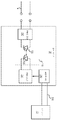
도 1은 본 발명의 실시예에 따른 버스 루프 시스템(100)을 도시한다. 버스 루프(100)는 호스트 시스템(1), 버스 루프(4), 버스 기기(10), 및 버스 기기(10)를 버스 루프(4)에 커플링하는 신호 처리기(30)를 포함한다. 호스트 시스템(1)은 버스 루프(4)를 통해 루프 전압(VL) 및 루프 전류(IL)를 생성한다. 호스트 시스템(1)은 중앙처리유닛(CPU), 또는 버스 루프(4)를 통해 수신되는 신호들을 처리하기 위해 사용되는 일부 다른 처리 시스템을 포함할 수 있다. 본 발명의 일 실시예에 따르면, 버스 루프(4)는 2선식 버스 루프(4)를 포함한다. 그러나, 버스 루프(4)는 2선식 버스 루프를 포함해야 하는 것은 아님이 이해되어야 한다.1 illustrates a
버스 기기(10)는 유량계(flow meter)와 같은 임의의 방식의 센서 또는 계측기를 포함한다. 버스 기기(10)가 유량계를 포함하는 실시예들에서, 유량계는 코리올리(Coriolis) 유량계 또는 농도계(densitometer)와 같은 진동 유량계를 포함할 수 있다. 도 1에 도시된 것처럼, 버스 기기(10)는 센서(13) 및 버스 기기 전자장치(20)를 포함할 수 있다. 버스 기기 전자장치(20)는 임의의 방식의 CPU, 프로세싱 시스템, 또는 마이크로-프로세싱 시스템을 포함할 수 있다. 본 발명의 일 실시예에 따르면, 센서(13)는 제1 아날로그 신호들을 생성하고 제1 아날로그 신호들을 버스 기기 전자장치(20)로 입력하도록 구성된다. 버스 기기 전자장치(20)는 버스 루프(4)에서 흐르는 가변 루프 전류(IL)의 형태인 제2 아날로그 신호들을 생성할 수 있다. 버스 기기(10)는 2선식 버스(4)와 함께 사용될 때 미리결정되거나 제한된 양의 전력을 인출(draw)하도록 구성될 수 있다. 버스 루프 시스템(100) 내에 형성되는 측정 통신 프로토콜 및 전력 제한들로 인하여, 버스 기기(10)는 신호 처리기(30)를 이용하여 2선식 버스 루프(4)로부터 절연될 수 있다. 일부 실시예들에서, 신호 처리기(30)는 본질안정(instrinsically safe; I.S.) 배리어(대시선)를 포함할 수 있다.The
절연은 버스 기기(10)가 2선식 버스 루프(4) 및 호스트 시스템(1)으로부터 인출할 수 있는 전기 전력을 제한한다. 절연은 버스 기기(10)의 파국적 고장의 경우에 2선식 버스 루프(4) 및 호스트 시스템(1)에 대한 손상을 방지한다. 또한, 절연은 버스 기기(10)의 환경에서 폭발 위험을 제거하고 임의의 폭발성 또는 가연성 물질들의 점화를 방지하기 위하여, I.S. 배리어를 통해 전기 전력 전달을 제한한다.Isolation limits the electrical power that the
도 2는 신호 처리기(30)의 절연 특징의 보다 구체적인 내용을 도시한다. 신호 처리기는 버스 기기(10)로부터 제1 아날로그 신호를 수신하는 것으로 도시된다. 그러나, 제1 아날로그 신호는 버스 기기(10)로부터 발신될 필요는 없고, 오히려 신호 처리기(30)는 아날로그 신호 처리가 요구되는 다른 환경들에서 이용될 수 있다. 리드들(220)을 통해 버스 기기(10)로부터 수신된 아날로그 신호는 신호들이 디지털화되는 아나로그-디지털 컨버터(240)에 의해 수신된다. 본 발명의 일 실시예에 따르면, 아날로그-디지털 컨버터(240)는 아날로그 신호를 직렬 비트 스트림으로 변환하는 델타 시그마 컨버터를 포함한다. 그러나, 다른 아날로그-디지털 컨버터들이 사용될 수 있고 특히 사용되는 아날로그-디지털 컨버터는 본 발명의 범위를 제한하지 않아야 함이 이해되어야 한다.2 shows more details of the isolation features of the
본 발명의 일 실시예에 따르면, 신호 처리기(30)는 2선식 버스 루프(4) 및 아날로그-디지털 컨버터(240) 사이에 연결되는 광커플러(115)를 포함한다. 광커플러(115)는 또한 광절연기, 광학 커플러, 또는 포토커플러로 지칭될 수도 있다. 광커플러(115)는 호스트 시스템(1)으로부터 버스 기기(10)를 전기적으로 절연시킨다. 결과적으로, 버스 기기(10)는 2선식 버스 루프(4)를 단락(short out)시킬 수 없다. 또한, 버스 기기(10)의 파국적 고장은 호스트 시스템(1)으로부터 과도한 전류를 인출할 수 없다. 송신기 및 수신기 광 소스들(122, 123)은 레이저 송신기 및 수신기 레이저 광 소스들, LED 송신기 및 수신기 광소스들, LED 레이저 송신기 및 수신기 광 소스들 등을 포함하는, 임의 방식의 광-반응 전자 컴포넌트들을 포함할 수 있다.According to one embodiment of the invention, the
송신기 광 소스(122) 및 수신기 광 소스(123)는 서로 인접하여 공동으로 형성되며, 송신기 광 소스(122)에 의해 생성되는 광은 수신기 광 소스(123)에 의해 직접 수신된다. 다른 실시예들에서, 송신기 광 소스(122) 및 수신기 광 소스(123)는 예를 들어 광섬유 케이블과 같은 일부 광학 디바이스에 의해 분리된다. 일부 실시예들에서, 상기 두 컴포넌트들은 도 2에서 도시된 단일 패키지로 형성된다. 그러나, 다른 실시예들에서, 송신기 광 소스(122) 및 수신기 광 소스(123)는 별도의 컴포넌트들을 포함할 수 있음이 이해되어야 한다.The
송신기 광 소스(122)는 전기 전류를 방사된 광으로 변환하는 것을 포함하는 광-인코딩된 신호를 생성한다. 수신기 광 소스(123)는 광-인코딩된 신호를 수신하고 수신된 광을 다시 송신기 광 소스(122)에서의 원래 전기 신호와 실질적으로 동일한 전기 신호로 변환한다. 광커플러(115)는 따라서 디지털 신호를 전달하는 데 잘 적응된다.
도 2에 도시된 실시예에서, 버스 기기(10)는 제1 아날로그 신호를 생성하고, 이는 아날로그-디지털 컨버터(240)로 송신된다. 아날로그-디지털 컨버터(240)는 디지털 신호를 출력한다. 디지털 신호는 송신기 광 소스(122)에 의해 수신되고 수신기 광 소스(123)로 송신된다. 수신기 광 소스(123)는 그 후 수신된 신호를 신호 스케일러(250)로 송신할 수 있다.In the embodiment shown in FIG. 2,
신호 스케일러(250)는 예를 들어 직렬 비트 스트림의 형태일 수 있는 디지털 신호들을 처리할 수 있고 디지털 신호를 스케일링된 펄스 폭 변조(PMW) 신호로 변환할 수 있다. PMW 신호는 그 후 제2 아날로그 신호로 변환될 수 있고 버스 루프(4)로 출력될 수 있다. 본 발명의 일 실시예에 따르면, 신호 스케일러(250)는 수신기 광 소스(123)로부터의 들어오는 비트 스트림을 스케일링하도록 구성된다. 스케일링은 임의의 방식의 선형 또는 비선형 스케일링을 포함할 수 있다. 스케일링은 디지털 신호의 펄스 폭 변조 신호로의 변환 이전에 또는 변환 동안 발생할 수 있다. 다른 실시예들에서, 스케일링은 디지털 신호의 펄스 폭 변조 신호로의 변환 이후에 발생할 수 있다. 이는 신호 처리기가 버스 루프(4)에 의해 사용되는 인코딩과 상이하게 인코딩되는 제1 아날로그 신호들을 수신하고 있는 상황들에서 유용할 수 있다. 예를 들어, 신호 처리기(30)가 유량계와 같은 12-20mA에 기초한 신호들(여기서 12mA는 0의 유량을 나타내고 20mA는 최대 유량을 나타냄)을 송신하는 버스 기기(10)에 결합되지만, 버스 루프(4)가 4-20mA 스케일(여기서 4mA는 0의 유량을 나타내고 20mA는 최대 유량을 나타냄)로 동작하고 있는 2선식 버스를 포함하는 상황이 그러하다. 비트 스트림을 스케일링 하지 않으면, 제2 아날로그 신호는 12-20mA 범위의 아날로그 신호들을 나타낼 것이다. 제2 아날로그 신호는 사실상 0의 유량이 존재할 때 시스템에서의 유량을 나타낼 것이다. 따라서, 비트 스트림을 스케일링하지 않으면, 에러는 시스템을 통하여 전파될 수 있다. 위에서 사용된 특정 값들은 단지 일 예로서 제공되고 특정 값들이 구체적 실시에 따라 변화함에 따라 본 발명의 범위를 제한하지 않아야 함이 이해되어야 한다.
본 발명의 일 실시예에 따른 신호 스케일러(250)는 들어오는 비트 스트림을 동시에 스케일링하면서 펄스 폭 변조 신호를 생성한다. 본 발명에 따른 신호 스케일러는 버스 기기(10) 및 버스 루프(4)에 의해 사용되는 신호의 인코딩에 있어서의 차에 기초하여 펄스 폭 변조 신호를 스케일링할 수 있다. 따라서, 신호 스케일러(250)에 의해 수행되는 스케일링은 호스트 시스템(1)에 의해 사용되는 신호 스케일을 수용하기 위한 펄스 폭 변조 신호의 스케일링을 포함할 수 있다. 본 발명의 일 실시예에 따르면, 신호 스케일러(250)는 다양한 버스 기기들(10)을 수용하기 위하여 펄스 폭 변조 신호를 스케일링할 수 있다.The
본 발명의 일 실시예에 따르면, 신호 스케일러(250)는 비트 스트림에서 논리 '0'과 논리 '1'을 나타내는 식들에 기초하여 스케일링된 PWM 신호를 생성한다. 예시적인 식들이 이하에서 식 1 및 식 2로서 도시된다. 식들 1 및 2는 단지 예들이고 다른 식들이 본 발명의 범위를 일탈함이 없이 펄스 폭 변조 신호를 생성하기 위해 이용될 수 있음이 이해되어야 한다.According to one embodiment of the invention,

여기서:here:


그리고 여기서 상수들은:And here the constants are:
R1 = 제1 임피던스R 1 = first impedance
R2 = 제2 임피던스R 2 = second impedance
Vref -1 = 제1 기준 전압V ref -1 = first reference voltage
Vref -2 = 제2 기준 전압V ref -2 = second reference voltage
Digoff -1 = 제1 디지털 오프셋Dig off -1 = first digital offset
Digper = 주기적 오프셋Dig per = periodic offset
DigFB -1 = 피드백 값Dig FB -1 = feedback value
I1 = 제1 전류I 1 = first current
I2 = 제2 전류I 2 = second current
식들 1 및 2는 식들에서 사용되는 상수들을 변화시킴으로써 조정될 수 있음이 이해되어야 한다. 상수들은 제1 및 제2 아날로그 신호 사이의 차들을 수용하도록 펄스 폭 변조 신호를 스케일링하기 위하여 변경될 수 있다. 구체적으로, 상수들은 제1 전류 및 제2 전류의 신호 인코딩 사이의 변화들을 수용하도록 변경될 수 있다. 식들은 시스템의 물리적 거동에 기초한다. 호스트 시스템(1)이 약 4-20mA 사이에서 동작하는 2선식 버스(4)에 결합되는 실시예들에서, 약 4mA의 제2 전류 I2는 0%에 대응하는 한편, 약 20mA의 제2 전류 값은 100%에 대응한다. 제1 전류 값들 I1은 제2 전류와 동일할 수 있거나, 즉 4mA-20mA이거나, 상이한 스케일, 예를 들어, 12mA-20mA일 수 있다. 따라서, 제1 스케일 및 제2 스케일이 상이한 실시예들에서, 상수 값들은 차에 대해 보상하도록 조정될 수 있고 따라서 버스 루프(4)에 의해 사용되는 아날로그 시그널링에 대응하는 스케일링된 펄스 폭 변조 신호를 생성할 수 있다.It should be understood that
제1 및 제2 시그널링 사이의 차들을 수용하기 위해 상수들을 조정하는 것에 부가하여, 상수들은 상이한 버스 기기들을 수용하기 위하여 조정될 수도 있다. 따라서, 비록 버스 기기(10) 및 호스트 시스템(1)이 동일한 시그널링을 이용한다 하더라도, 신호 스케일러(250)는 센서들(13) 사이의 차들에 대해 신호를 조정하도록 신호를 스케일링할 수 있다. 따라서, 동일한 신호 처리기(30)가 식들 1 및 2로의 상수 입력을 간단히 변경함으로써 다수의 환경들에서 다수의 센서들과 함께 사용될 수 있다. 상수들은 신호 처리기(30)의 내부 또는 외부 시스템에 저장되거나, 사용자/운용자에 의해 수동으로 입력되는 검색 테이블의 형태로 존재할 수 있다.In addition to adjusting the constants to accommodate the differences between the first and second signaling, the constants may be adjusted to accommodate different bus devices. Thus, although
일단 신호 스케일러(250)가 비트 스트림에 기초하여 스케일링된 펄스 폭 변조 신호를 생성하면, 스케일링된 펄스 폭 변조 신호는 호스트 시스템(1)에 의해 사용되는 아날로그 시그널링에 대응하는 제2 아날로그 시그널로 변환된다. 호스트 시스템(1)은 신호의 어떠한 추가적인 스케일링도 수행하도록 요구되지 않음이 이해되어야 한다. 오히려 신호의 모든 요구되는 스케일링은 신호 스케일러(250)에 의해 이미 수행된다.Once the
도 3은 본 발명의 일 실시예에 따른 신호 스케일러(250)에 의해 수행되는 알고리즘(300)을 도시한다. 알고리즘은 비트 스트림이 광커플러(115)로부터 수신되는 단계 301에서 시작한다. 비트 스트림 값이 1과 같다면, 알고리즘은 식 1로부터의 'A' 값을 신호 스케일러(250)의 누산기(비도시)에 부가함으로써 펄스 폭 값이 계산되는 단계 302로 이동한다. 한편, 비트스트림 값이 0과 같다면, 알고리즘은 식 2로부터의 'B' 값을 누산기에 부가함으로써 펄스 폭 값이 계산되는 단계 303으로 이동한다. 따라서, 누산기는 비트 스트림에서 'A' 및 'B' 값들의 수에 기초하여 펄스 폭 변조 신호를 생성한다. 스케일링된 PWM 신호는 그 후 단계 404에서 출력될 수 있다. 일단 신호가 송신되면, 알고리즘은 단계 301로 복귀한다. 'A' 및 'B' 값들에 기초하여, 신호 스케일러(250)는 제1 아날로그 신호 인코딩이 아닌 제2 아날로그 신호 인코딩에 대응하는 스케일링된 펄스 폭 변조 신호를 생성할 수 있다. 따라서, 신호 스케일러(250)가 펄스 폭 변조 신호를 제2 아날로그 신호로 변환할 때, 정확한 값은 제2 아날로그 신호로 표현된다. 따라서, 비록 버스 기기(10)가 12-20 mA 스케일에서 동작하고 있다 하더라도, 생성된 펄스 폭 변조 신호는 호스트 시스템(1) 및 버스 루프(4)에 의해 사용되는 4-20 mA에 대응한다. 스케일링은 버스 기기(10) 및 호스트 시스템(1) 사이의 시그널링에 있어서의 차로 인해 에러가 발생하는 것을 실질적으로 방지한다.3 illustrates an
도 4는 본 발명의 또 다른 실시예에 따른 신호 처리기(30)를 도시한다. 도 4에 도시된 신호 처리기(30)는 제1 아날로그 신호를 수신하고, 아날로그 신호를 디지털 표현으로 변환하고, 디지털 신호에 기초하여 PWM 신호를 생성하고, PWM 신호를 광커플러를 통해 송신하고, PWM 신호를 PWM 디코더(442)를 이용하여 스케일링하고, 스케일링된 신호를 다시 제2 아날로그 신호로 변환하도록 구성되며, 제1 및 제2 아날로그 신호는 동일한 값을 포함할 수도 있고 포함하지 않을 수도 있다. 도 2에 도시된 컴포넌트들에 부가하여, 도 5의 신호 처리기(30)는 펄스 폭 생성기(241) 및 펄스 폭 디코더(242)를 또한 포함한다. 본 발명의 일 실시예에 따르면, 펄스 폭 생성기(241)는 아날로그-디지털 컨버터(240)로부터 수신된 직렬 비트 스트림에 기초하여 PWM 신호를 생성한다. PWM 신호는 그 후 광커플러(115)를 통해 송신될 수 있다. 본 발명의 일 실시예에 따르면, 펄스 폭 디코더(242)는 수신기 광 소스(123)로부터 수신된 PWM 신호를 버스 루프(4)에 의해 이용가능한 신호로 스케일링한다. 스케일링된 PWM 신호는 그 후 제2 아날로그 신호로 변환되고 버스 루프(4)로 출력될 수 있다. 이는 PWM 신호를 생성하면서 신호를 스케일링하는 도 2에 도시된 신호 처리기와 대조된다. 따라서, 도 4의 신호 처리기(30)는 PWM 신호를 스케일링하기 위하여 펄스 폭 디코더(242)를 요함으로써 추가적인 단계를 요한다. 그러나, 도 4의 전체적인 신호 처리기(30)는 여전히 신호를 버스 루프(4)에 출력하기 전에 신호를 스케일링할 수 있음이 이해되어야 한다. 따라서, 버스 기기(10) 및 호스트 시스템(1)는 여전히 상이한 시그널링 또는 상이한 스케일들을 이용하여 동작할 수 있다.4 shows a
본 발명의 다른 실시예에 따르면, 펄스 폭 생성기(241)는 신호를 광커플러(115)로 송신하기 전에 전술한 것처럼 PWM 신호를 스케일링한다. 따라서, 펄스 폭 디코더(242)는 신호를 버스 루프(4)로 출력하기 전에 스케일링된 PWM 신호를 제2 아날로그 신호로 변환할 필요만이 있다.According to another embodiment of the invention, the
비록 전술한 기재는 신호 처리기(30)를 버스 기기(10)로부터 이격된 컴포넌트를 포함하는 것으로서 기재되었지만, 일부 실시예들에서는, 신호 처리기(30)는 버스 기기(10)의 일체화된 컴포넌트를 포함함이 이해되어야 한다. 따라서, 본 발명의 일 실시예에 따르면, 버스 기기 전자장치(20)는 스케일링된 PWM 신호를 생성할 수 있고 스케일링된 PWM 신호를 신호 출력 이전에 제2 아날로그 신호로 변환할 수 있다. 또한, 전술한 기재가 버스 기기(10)와 조합된 신호 처리기(30)를 논의하였지만, 신호 처리기(30) 내에서 발생하는 스케일링은 임의의 입력 아날로그 신호에 동등하게 적용가능함이 이해되어야 한다. 또한, 신호 처리기(30)는 버스 루프(4)에 연결될 필요가 없다. 이러한 컴포넌트들과 관련한 본 발명의 논의는 단지 본 발명의 이해를 돕기 위한 목적을 위한 것이고, 어떠한 방식으로도 본 발명의 범위를 제한하지 않아야 한다.Although the foregoing description has been described as including a component that separates the
전술한 청구된 발명은 상이한 인코딩 방식들 하에서 동작할 수 있는 둘 이상의 루프 시스템들 사이에 신호를 송신할 수 있는 신호 처리 시스템(100)을 제공한다. 신호 처리 시스템(100)은 제1 아날로그 신호가 아닌 제2 아날로그 신호의 인코딩 방식에 대응하는 신호로 입력 디지털 신호를 스케일링하도록 구성된다. 따라서, 전달된 디지털 신호는 추가의 처리 없이 아날로그 신호로 다시 변환될 수 있다.The claimed invention described above provides a
상기 실시예들의 세부적 기재들은 본 발명의 범위 내에 있도록 발명자들에 의해 고려된 모든 실시예들의 완벽한 기재들은 아니다. 사실, 당업자는 전술한 실시예들의 특정 요소들이 추가의 실시예들을 생성하기 위하여 다양하게 결합되거나 제거될 수 있고, 이러한 추가의 실시예들은 본 발명의 범위 및 교시 내에 든다는 것을 인식할 것이다. 전술한 실시예들은 본 발명의 범위 또는 교시 내에 드는 추가의 실시예들을 생성하기 위하여 전체적으로 또는 부분적으로 결합될 수 있음이 당업자에게 명백할 것이다. The detailed descriptions of the above embodiments are not exhaustive of all the embodiments considered by the inventors to be within the scope of the present invention. In fact, those skilled in the art will recognize that certain elements of the above-described embodiments may be variously combined or eliminated to create further embodiments, and such additional embodiments are within the scope and teaching of the present invention. It will be apparent to those skilled in the art that the above-described embodiments may be combined in whole or in part to create further embodiments that fall within the scope or teaching of the present invention.
따라서, 비록 본 발명의 구체적 실시예들 및 예시들이 여기에 설명 목적을 위하여 기재되었지만, 관련 기술분야의 당업자가 인식할 것처럼 다양한 등가의 수정들이 본 발명의 범위 내에서 가능하다. 여기에 제공된 교시들은 다른 버스 루프 전자장치에 적용될 수 있고, 위에서 기재되고 첨부 도면들에서 도시된 실시예들에만 적용되지는 않는다. 따라서, 본 발명의 범위는 다음 청구범위로부터 결정되어야 한다.
Thus, although specific embodiments and examples of the invention have been described herein for purposes of illustration, various equivalent modifications are possible within the scope of the invention as will be appreciated by those skilled in the art. The teachings provided herein can be applied to other bus loop electronics and are not limited to the embodiments described above and shown in the accompanying figures. Accordingly, the scope of the invention should be determined from the following claims.
Claims (15)
상기 제1 아날로그 신호를 디지털 신호로 변환하고;
상기 디지털 신호를 전기 배리어를 가로질러 송신하고,
상기 디지털 신호에 기초하고 제1 아날로그 신호 인코딩 및 제2 아날로그 신호 인코딩 사이의 차에 기초하여, 스케일링된 펄스 폭 변조 신호를 생성하고; 그리고
상기 스케일링된 펄스 폭 변조 신호를 제2 아날로그 신호로 변환하도록
구성된 신호 처리기(30).Receive a first analog signal;
Converting the first analog signal into a digital signal;
Transmit the digital signal across an electrical barrier,
Generate a scaled pulse width modulated signal based on the digital signal and based on a difference between a first analog signal encoding and a second analog signal encoding; And
To convert the scaled pulse width modulated signal to a second analog signal
Configured signal processor 30.
상기 전기 배리어는 광커플러(optocoupler, 115)를 포함하는,
신호 처리기(30).The method of claim 1,
The electrical barrier comprises an optocoupler 115,
Signal processor 30.
상기 제1 아날로그 신호 인코딩은 상기 신호 처리기(30)의 입력에 결합된 버스 기기(10)에 의해 이용되고, 상기 제2 아날로그 신호 인코딩은 상기 신호 처리기(30)의 출력에 결합된 버스 루프(4)에 의해 이용되는,
신호 처리기(30).The method of claim 1,
The first analog signal encoding is used by a bus device 10 coupled to the input of the signal processor 30, and the second analog signal encoding is bus loop 4 coupled to the output of the signal processor 30. Used by),
Signal processor 30.
상기 디지털 신호는 직렬 비트 스트림을 포함하는,
신호 처리기(30).The method of claim 1,
The digital signal comprises a serial bit stream,
Signal processor 30.
신호 처리기(30)에 의해 버스 루프(40)로부터 전기적으로 절연된 버스 기기(10)에 의해 수신된 상기 제1 아날로그 신호를 상기 디지털 신호로 변환하도록 적응된 아날로그-디지털 컨버터(240); 및
상기 디지털 신호를 신호 스케일러(250)로 송신하도록 적응된 신호 송신기(115)를 포함하고,
상기 신호 스케일러(250)는, 상기 디지털 신호를 스케일링된 펄스 폭 변조 신호로 변환하고 상기 스케일링된 펄스 폭 변조 신호를 스케일링된 제2 아날로그 신호로 변환하도록 적응되는,
신호 처리기(30).The method of claim 1,
An analog-to-digital converter (240) adapted to convert the first analog signal received by the bus device (10) electrically isolated from the bus loop (40) by a signal processor (30) into the digital signal; And
A signal transmitter 115 adapted to transmit the digital signal to a signal scaler 250,
The signal scaler 250 is adapted to convert the digital signal into a scaled pulse width modulated signal and to convert the scaled pulse width modulated signal into a scaled second analog signal,
Signal processor 30.
상기 신호 송신기(115)는 상기 버스 기기(10)를 상기 버스 루프(4)로부터 전기적으로 절연시키도록 적응된 광커플러를 포함하는,
신호 처리기(30).The method of claim 5, wherein
The signal transmitter 115 comprises an optocoupler adapted to electrically insulate the bus device 10 from the bus loop 4,
Signal processor 30.
상기 제1 아날로그 신호 인코딩은 상기 제2 아날로그 신호 인코딩과 상이한,
신호 처리기(30).The method of claim 1,
The first analog signal encoding is different from the second analog signal encoding,
Signal processor 30.
상기 제1 아날로그 신호를 디지털 신호로 변환하고;
상기 디지털 신호에 기초하여 펄스 폭 변조 신호를 생성하고;
상기 펄스 폭 변조 신호를 전기 배리어를 가로질러 송신하고; 그리고
제1 아날로그 신호 인코딩 및 제2 아날로그 신호 인코딩 사이의 차에 기초하여, 상기 펄스 폭 변조 신호를 스케일링된 제2 아날로그 신호로 변환하도록
구성된 신호 처리기(30).Receive a first analog signal;
Converting the first analog signal into a digital signal;
Generate a pulse width modulated signal based on the digital signal;
Transmit the pulse width modulated signal across an electrical barrier; And
Based on the difference between the first analog signal encoding and the second analog signal encoding, to convert the pulse width modulated signal to a scaled second analog signal.
Configured signal processor 30.
상기 제1 아날로그 신호 인코딩은 상기 신호 처리기(30)의 입력에 결합된 버스 기기(10)에 의해 이용되고, 상기 제2 아날로그 신호 인코딩은 상기 신호 처리기(30)의 출력에 결합된 버스 루프(4)에 의해 이용되는,
신호 처리기(30).The method of claim 8,
The first analog signal encoding is used by a bus device 10 coupled to the input of the signal processor 30, and the second analog signal encoding is bus loop 4 coupled to the output of the signal processor 30. Used by),
Signal processor 30.
제1 아날로그 신호를 생성하는 단계;
상기 제1 아날로그 신호를 디지털 신호로 변환하는 단계;
상기 디지털 신호를 전기 배리어를 가로질러 송신하는 단계;
상기 디지털 신호에 기초하고 제1 아날로그 신호 인코딩 및 제2 아날로그 신호 인코딩 사이의 차에 기초하여, 스케일링된 펄스 폭 변조 신호를 생성하는 단계; 및
상기 스케일링된 펄스 폭 변조 신호를 스케일링된 제2 아날로그 신호로 변환하는 단계를 포함하는,
신호들을 아날로그 신호 생성기로부터 아날로그 신호 수신기로 송신하기 위한 방법.A method for transmitting signals from an analog signal generator to an analog signal receiver, the method comprising:
Generating a first analog signal;
Converting the first analog signal into a digital signal;
Transmitting the digital signal across an electrical barrier;
Generating a scaled pulse width modulated signal based on the digital signal and based on a difference between a first analog signal encoding and a second analog signal encoding; And
Converting the scaled pulse width modulated signal to a scaled second analog signal,
A method for transmitting signals from an analog signal generator to an analog signal receiver.
상기 디지털 신호를 송신하기 위하여 광커플러를 이용하는 단계를 더 포함하는,
신호들을 아날로그 신호 생성기로부터 아날로그 신호 수신기로 송신하기 위한 방법.11. The method of claim 10,
Further comprising using an optocoupler to transmit the digital signal;
A method for transmitting signals from an analog signal generator to an analog signal receiver.
상기 스케일링된 제2 아날로그 신호는 상기 아날로그 신호 생성기에 의해 이용되는 상기 제1 아날로그 신호 인코딩 및 상기 아날로그 신호 수신기에 의해 이용되는 상기 제2 아날로그 신호 인코딩 사이의 차에 기초하는,
신호들을 아날로그 신호 생성기로부터 아날로그 신호 수신기로 송신하기 위한 방법.11. The method of claim 10,
The scaled second analog signal is based on a difference between the first analog signal encoding used by the analog signal generator and the second analog signal encoding used by the analog signal receiver,
A method for transmitting signals from an analog signal generator to an analog signal receiver.
제1 아날로그 신호를 수신하는 단계;
상기 제1 아날로그 신호를 디지털 신호로 변환하는 단계;
상기 디지털 신호에 기초하여 펄스 폭 변조 신호를 생성하는 단계;
상기 펄스 폭 변조 신호를 전기 배리어를 가로질러 송신하는 단계; 및
제1 아날로그 신호 인코딩 및 제2 아날로그 신호 인코딩 사이의 차에 기초하여 상기 펄스 폭 변조 신호를 스케일링된 제2 아날로그 신호로 변환하는 단계를 포함하는,
신호들을 아날로그 신호 생성기로부터 아날로그 신호 수신기로 송신하기 위한 방법.A method for transmitting signals from an analog signal generator to an analog signal receiver, the method comprising:
Receiving a first analog signal;
Converting the first analog signal into a digital signal;
Generating a pulse width modulated signal based on the digital signal;
Transmitting the pulse width modulated signal across an electrical barrier; And
Converting the pulse width modulated signal to a scaled second analog signal based on a difference between a first analog signal encoding and a second analog signal encoding,
A method for transmitting signals from an analog signal generator to an analog signal receiver.
상기 디지털 신호를 송신하기 위하여 광커플러를 이용하는 단계를 더 포함하는,
신호들을 아날로그 신호 생성기로부터 아날로그 신호 수신기로 송신하기 위한 방법.The method of claim 13,
Further comprising using an optocoupler to transmit the digital signal;
A method for transmitting signals from an analog signal generator to an analog signal receiver.
상기 스케일링된 제2 아날로그 신호는 상기 아날로그 신호 생성기에 의해 이용되는 상기 제1 아날로그 신호 인코딩 및 상기 아날로그 신호 수신기에 의해 이용되는 상기 제2 아날로그 신호 인코딩 사이의 차에 기초하는,
신호들을 아날로그 신호 생성기로부터 아날로그 신호 수신기로 송신하기 위한 방법.The method of claim 13,
The scaled second analog signal is based on a difference between the first analog signal encoding used by the analog signal generator and the second analog signal encoding used by the analog signal receiver,
A method for transmitting signals from an analog signal generator to an analog signal receiver.
Applications Claiming Priority (1)
| Application Number | Priority Date | Filing Date | Title |
|---|---|---|---|
| PCT/US2008/071564 WO2010014085A1 (en) | 2008-07-30 | 2008-07-30 | Method and apparatus for pulse width modulation signal processing |
Publications (2)
| Publication Number | Publication Date |
|---|---|
| KR20110049839A KR20110049839A (en) | 2011-05-12 |
| KR101231131B1 true KR101231131B1 (en) | 2013-02-07 |
Family
ID=40456257
Family Applications (1)
| Application Number | Title | Priority Date | Filing Date |
|---|---|---|---|
| KR1020117004799A KR101231131B1 (en) | 2008-07-30 | 2008-07-30 | Method and apparatus for pulse width modulation signal processing |
Country Status (12)
| Country | Link |
|---|---|
| US (1) | US8531326B2 (en) |
| EP (1) | EP2313996B9 (en) |
| JP (1) | JP5315413B2 (en) |
| KR (1) | KR101231131B1 (en) |
| CN (1) | CN102113244B (en) |
| AR (1) | AR072529A1 (en) |
| AU (1) | AU2008360008B2 (en) |
| BR (1) | BRPI0822970B1 (en) |
| CA (1) | CA2731431C (en) |
| HK (1) | HK1159344A1 (en) |
| MX (1) | MX2011000752A (en) |
| WO (1) | WO2010014085A1 (en) |
Families Citing this family (3)
| Publication number | Priority date | Publication date | Assignee | Title |
|---|---|---|---|---|
| RU2549203C2 (en) | 2010-09-13 | 2015-04-20 | Майкро Моушн, Инк. | Opto-isolator circuit |
| JP5611906B2 (en) * | 2011-08-12 | 2014-10-22 | 株式会社東芝 | Semiconductor device, inspection method thereof and transmission circuit |
| US20130214601A1 (en) * | 2012-02-20 | 2013-08-22 | System General Corp. | Interface circuits for cascade and series battery management and methods thereof |
Citations (2)
| Publication number | Priority date | Publication date | Assignee | Title |
|---|---|---|---|---|
| US5434694A (en) * | 1992-03-31 | 1995-07-18 | Yokogawa Electric Corporation | Signal isolating device |
| US5949085A (en) * | 1997-01-29 | 1999-09-07 | Xircom, Inc. | Ratiometric compensated optical isolation coupler |
Family Cites Families (19)
| Publication number | Priority date | Publication date | Assignee | Title |
|---|---|---|---|---|
| US3794841A (en) * | 1972-07-25 | 1974-02-26 | L Cosentino | Light coupling data transfer system |
| JPS63121309A (en) * | 1986-11-10 | 1988-05-25 | Oki Electric Ind Co Ltd | Photocoupler for analog signal |
| RU2000658C1 (en) | 1990-10-09 | 1993-09-07 | Инженерно-научный центр "ТЭМП" | Width-modulated signal converter |
| JPH05282586A (en) * | 1992-04-03 | 1993-10-29 | Yokogawa Electric Corp | Signal transmitter |
| US5287107A (en) * | 1992-06-05 | 1994-02-15 | Hewlett-Packard Company | Optical isolation amplifier with sigma-delta modulation |
| US5435694A (en) * | 1993-11-19 | 1995-07-25 | General Electric Company | Stress relieving mount for an axial blade |
| US5995252A (en) | 1997-03-03 | 1999-11-30 | Elsag International N.V. | Low power digital signal isolator |
| US5875235A (en) * | 1997-03-07 | 1999-02-23 | S3, Incorporated | Transformerless data access arrangement |
| US6430229B1 (en) * | 1997-04-22 | 2002-08-06 | Silicon Laboratories Inc. | Capacitive isolation system with digital communication and power transfer |
| US5949225A (en) * | 1998-03-19 | 1999-09-07 | Astec International Limited | Adjustable feedback circuit for adaptive opto drives |
| US6321075B1 (en) | 1998-07-30 | 2001-11-20 | Qualcomm Incorporated | Hardware-efficient transceiver with delta-sigma digital-to-analog converter |
| US6535564B1 (en) * | 1999-04-09 | 2003-03-18 | Nokia Mobile Phones Ltd. | Adaptive quantization in a pulse-amplitude modulated system |
| FI107545B (en) | 1999-06-15 | 2001-08-31 | Kemira Chemicals Oy | Process for processing mechanical masses |
| JP4871458B2 (en) * | 2001-06-13 | 2012-02-08 | 株式会社高見沢サイバネティックス | Data conversion device and telemeter device |
| JP2004157840A (en) * | 2002-11-07 | 2004-06-03 | Inc Engineering Co Ltd | Signal converter |
| JP2006303663A (en) * | 2005-04-18 | 2006-11-02 | Nec Electronics Corp | Optically-coupled isolation circuit |
| US8237496B2 (en) * | 2010-07-29 | 2012-08-07 | Broadcom Corporation | Switching amplifier with enhanced supply rejection and related method |
| US8462003B2 (en) * | 2010-09-21 | 2013-06-11 | Avago Technologies General Ip (Singapore) Pte. Ltd. | Transmitting and receiving digital and analog signals across an isolator |
| US8217820B2 (en) * | 2010-11-04 | 2012-07-10 | Maxim Integrated Products, Inc. | Using multi-level pulse width modulated signal for real time noise cancellation |
-
2008
- 2008-07-30 BR BRPI0822970-8A patent/BRPI0822970B1/en active IP Right Grant
- 2008-07-30 MX MX2011000752A patent/MX2011000752A/en active IP Right Grant
- 2008-07-30 AU AU2008360008A patent/AU2008360008B2/en active Active
- 2008-07-30 JP JP2011521075A patent/JP5315413B2/en active Active
- 2008-07-30 EP EP08782510.5A patent/EP2313996B9/en active Active
- 2008-07-30 CN CN200880130576.2A patent/CN102113244B/en active Active
- 2008-07-30 US US13/003,822 patent/US8531326B2/en active Active
- 2008-07-30 CA CA2731431A patent/CA2731431C/en active Active
- 2008-07-30 KR KR1020117004799A patent/KR101231131B1/en active IP Right Grant
- 2008-07-30 WO PCT/US2008/071564 patent/WO2010014085A1/en active Application Filing
-
2009
- 2009-07-22 AR ARP090102792A patent/AR072529A1/en active IP Right Grant
-
2011
- 2011-12-21 HK HK11113789.5A patent/HK1159344A1/en unknown
Patent Citations (2)
| Publication number | Priority date | Publication date | Assignee | Title |
|---|---|---|---|---|
| US5434694A (en) * | 1992-03-31 | 1995-07-18 | Yokogawa Electric Corporation | Signal isolating device |
| US5949085A (en) * | 1997-01-29 | 1999-09-07 | Xircom, Inc. | Ratiometric compensated optical isolation coupler |
Also Published As
| Publication number | Publication date |
|---|---|
| WO2010014085A1 (en) | 2010-02-04 |
| JP5315413B2 (en) | 2013-10-16 |
| JP2011529667A (en) | 2011-12-08 |
| AR072529A1 (en) | 2010-09-01 |
| BRPI0822970A2 (en) | 2015-06-23 |
| CA2731431C (en) | 2017-06-13 |
| AU2008360008B2 (en) | 2013-08-01 |
| EP2313996A1 (en) | 2011-04-27 |
| AU2008360008A1 (en) | 2010-02-04 |
| MX2011000752A (en) | 2011-03-21 |
| CN102113244B (en) | 2015-12-02 |
| EP2313996B9 (en) | 2019-10-09 |
| HK1159344A1 (en) | 2012-07-27 |
| US8531326B2 (en) | 2013-09-10 |
| CN102113244A (en) | 2011-06-29 |
| BRPI0822970B1 (en) | 2020-10-06 |
| US20110115657A1 (en) | 2011-05-19 |
| CA2731431A1 (en) | 2010-02-04 |
| KR20110049839A (en) | 2011-05-12 |
| EP2313996B1 (en) | 2018-10-24 |
Similar Documents
| Publication | Publication Date | Title |
|---|---|---|
| US8731846B2 (en) | Measuring arrangement for registering chemical and/or physical, measured variables, as well as measuring device therefor | |
| KR101231131B1 (en) | Method and apparatus for pulse width modulation signal processing | |
| US10855310B2 (en) | Data translation system and method comprising an optocoupler transmission system with a controller to determine transmission communication between devices | |
| RU2467476C2 (en) | Method and device for processing pulse width modulated signals | |
| CA2897023C (en) | Data translation system and method | |
| RU2323417C2 (en) | Measuring instrument with two-lead bus | |
| SG192522A1 (en) | Data translation system and method | |
| JP2012168955A (en) | Data translation system and method | |
| JP2014197896A (en) | Data translation system and method |
Legal Events
| Date | Code | Title | Description |
|---|---|---|---|
| A201 | Request for examination | ||
| E701 | Decision to grant or registration of patent right | ||
| GRNT | Written decision to grant | ||
| FPAY | Annual fee payment |
Payment date: 20160122 Year of fee payment: 4 |
|
| FPAY | Annual fee payment |
Payment date: 20170125 Year of fee payment: 5 |
|
| FPAY | Annual fee payment |
Payment date: 20180125 Year of fee payment: 6 |
|
| FPAY | Annual fee payment |
Payment date: 20190123 Year of fee payment: 7 |
|
| FPAY | Annual fee payment |
Payment date: 20200123 Year of fee payment: 8 |