KR100958464B1 - Infrared thermopile detector system semiconductor process monitoring and control - Google Patents
Infrared thermopile detector system semiconductor process monitoring and control Download PDFInfo
- Publication number
- KR100958464B1 KR100958464B1 KR1020047017524A KR20047017524A KR100958464B1 KR 100958464 B1 KR100958464 B1 KR 100958464B1 KR 1020047017524 A KR1020047017524 A KR 1020047017524A KR 20047017524 A KR20047017524 A KR 20047017524A KR 100958464 B1 KR100958464 B1 KR 100958464B1
- Authority
- KR
- South Korea
- Prior art keywords
- thermopile detector
- infrared
- semiconductor
- unit
- thermopile
- Prior art date
Links
- 238000000034 method Methods 0.000 title claims abstract description 143
- 230000008569 process Effects 0.000 title claims abstract description 116
- 239000004065 semiconductor Substances 0.000 title claims abstract description 73
- 238000012544 monitoring process Methods 0.000 title claims abstract description 24
- 230000007717 exclusion Effects 0.000 claims description 46
- 239000000463 material Substances 0.000 claims description 36
- 238000004140 cleaning Methods 0.000 claims description 27
- 238000012545 processing Methods 0.000 claims description 27
- 239000000126 substance Substances 0.000 claims description 22
- 239000011538 cleaning material Substances 0.000 claims description 16
- 239000012530 fluid Substances 0.000 claims description 16
- 238000005070 sampling Methods 0.000 claims description 15
- 230000005855 radiation Effects 0.000 claims description 13
- 239000000376 reactant Substances 0.000 claims description 13
- 238000011144 upstream manufacturing Methods 0.000 claims description 11
- 238000001514 detection method Methods 0.000 claims description 8
- 238000000151 deposition Methods 0.000 claims description 6
- 230000008021 deposition Effects 0.000 claims description 6
- 238000010521 absorption reaction Methods 0.000 claims description 5
- 239000007788 liquid Substances 0.000 claims description 4
- 230000003647 oxidation Effects 0.000 claims description 4
- 238000007254 oxidation reaction Methods 0.000 claims description 4
- 238000004886 process control Methods 0.000 claims description 4
- 238000011112 process operation Methods 0.000 claims description 3
- 239000007787 solid Substances 0.000 claims 2
- 238000005229 chemical vapour deposition Methods 0.000 claims 1
- 238000005468 ion implantation Methods 0.000 claims 1
- 230000026676 system process Effects 0.000 claims 1
- 230000003750 conditioning effect Effects 0.000 abstract description 3
- 230000000694 effects Effects 0.000 abstract description 2
- 239000007789 gas Substances 0.000 description 55
- 239000002699 waste material Substances 0.000 description 29
- 230000008054 signal transmission Effects 0.000 description 13
- 230000004044 response Effects 0.000 description 10
- 238000004519 manufacturing process Methods 0.000 description 9
- RBFQJDQYXXHULB-UHFFFAOYSA-N arsane Chemical compound [AsH3] RBFQJDQYXXHULB-UHFFFAOYSA-N 0.000 description 7
- 238000006243 chemical reaction Methods 0.000 description 6
- PQDJYEQOELDLCP-UHFFFAOYSA-N trimethylsilane Chemical compound C[SiH](C)C PQDJYEQOELDLCP-UHFFFAOYSA-N 0.000 description 6
- 229940094989 trimethylsilane Drugs 0.000 description 6
- 238000005259 measurement Methods 0.000 description 5
- 230000003595 spectral effect Effects 0.000 description 5
- 230000009977 dual effect Effects 0.000 description 4
- 239000002994 raw material Substances 0.000 description 4
- 230000001105 regulatory effect Effects 0.000 description 4
- 238000005033 Fourier transform infrared spectroscopy Methods 0.000 description 3
- 238000002835 absorbance Methods 0.000 description 3
- 230000005540 biological transmission Effects 0.000 description 3
- 238000011088 calibration curve Methods 0.000 description 3
- 238000010586 diagram Methods 0.000 description 3
- 239000000203 mixture Substances 0.000 description 3
- 239000002243 precursor Substances 0.000 description 3
- 229910000077 silane Inorganic materials 0.000 description 3
- 238000004611 spectroscopical analysis Methods 0.000 description 3
- 231100000331 toxic Toxicity 0.000 description 3
- 230000002588 toxic effect Effects 0.000 description 3
- XYFCBTPGUUZFHI-UHFFFAOYSA-N Phosphine Chemical compound P XYFCBTPGUUZFHI-UHFFFAOYSA-N 0.000 description 2
- BLRPTPMANUNPDV-UHFFFAOYSA-N Silane Chemical compound [SiH4] BLRPTPMANUNPDV-UHFFFAOYSA-N 0.000 description 2
- 238000004458 analytical method Methods 0.000 description 2
- 239000007864 aqueous solution Substances 0.000 description 2
- 230000001276 controlling effect Effects 0.000 description 2
- 238000012806 monitoring device Methods 0.000 description 2
- 125000002524 organometallic group Chemical class 0.000 description 2
- 239000000047 product Substances 0.000 description 2
- 150000004756 silanes Chemical class 0.000 description 2
- 238000001179 sorption measurement Methods 0.000 description 2
- 238000001228 spectrum Methods 0.000 description 2
- 238000012360 testing method Methods 0.000 description 2
- 239000002912 waste gas Substances 0.000 description 2
- JBRZTFJDHDCESZ-UHFFFAOYSA-N AsGa Chemical compound [As]#[Ga] JBRZTFJDHDCESZ-UHFFFAOYSA-N 0.000 description 1
- WKBOTKDWSSQWDR-UHFFFAOYSA-N Bromine atom Chemical class [Br] WKBOTKDWSSQWDR-UHFFFAOYSA-N 0.000 description 1
- ZAMOUSCENKQFHK-UHFFFAOYSA-N Chlorine atom Chemical class [Cl] ZAMOUSCENKQFHK-UHFFFAOYSA-N 0.000 description 1
- 229910001218 Gallium arsenide Inorganic materials 0.000 description 1
- 238000012369 In process control Methods 0.000 description 1
- 230000002378 acidificating effect Effects 0.000 description 1
- 229910052785 arsenic Inorganic materials 0.000 description 1
- RQNWIZPPADIBDY-UHFFFAOYSA-N arsenic atom Chemical compound [As] RQNWIZPPADIBDY-UHFFFAOYSA-N 0.000 description 1
- GDTBXPJZTBHREO-UHFFFAOYSA-N bromine Chemical class BrBr GDTBXPJZTBHREO-UHFFFAOYSA-N 0.000 description 1
- 229910052794 bromium Inorganic materials 0.000 description 1
- 239000006227 byproduct Substances 0.000 description 1
- 230000003197 catalytic effect Effects 0.000 description 1
- 230000008859 change Effects 0.000 description 1
- 239000007810 chemical reaction solvent Substances 0.000 description 1
- 229910052801 chlorine Inorganic materials 0.000 description 1
- 239000000460 chlorine Chemical class 0.000 description 1
- 238000004891 communication Methods 0.000 description 1
- 238000012937 correction Methods 0.000 description 1
- 238000000354 decomposition reaction Methods 0.000 description 1
- 230000003247 decreasing effect Effects 0.000 description 1
- 238000005137 deposition process Methods 0.000 description 1
- 238000011161 development Methods 0.000 description 1
- 230000018109 developmental process Effects 0.000 description 1
- 238000007599 discharging Methods 0.000 description 1
- 239000006185 dispersion Substances 0.000 description 1
- 238000006073 displacement reaction Methods 0.000 description 1
- 238000005516 engineering process Methods 0.000 description 1
- 229910000078 germane Inorganic materials 0.000 description 1
- 231100001261 hazardous Toxicity 0.000 description 1
- 239000002920 hazardous waste Substances 0.000 description 1
- 238000010965 in-process control Methods 0.000 description 1
- 238000010978 in-process monitoring Methods 0.000 description 1
- 230000031700 light absorption Effects 0.000 description 1
- 125000002496 methyl group Chemical group [H]C([H])([H])* 0.000 description 1
- 238000012986 modification Methods 0.000 description 1
- 230000004048 modification Effects 0.000 description 1
- 230000005693 optoelectronics Effects 0.000 description 1
- 229910000073 phosphorus hydride Inorganic materials 0.000 description 1
- 238000002360 preparation method Methods 0.000 description 1
- 230000009467 reduction Effects 0.000 description 1
- 238000004088 simulation Methods 0.000 description 1
- 239000008247 solid mixture Substances 0.000 description 1
- 239000010891 toxic waste Substances 0.000 description 1
- 238000010977 unit operation Methods 0.000 description 1
- 238000007740 vapor deposition Methods 0.000 description 1
- XLYOFNOQVPJJNP-UHFFFAOYSA-N water Substances O XLYOFNOQVPJJNP-UHFFFAOYSA-N 0.000 description 1
- 238000005200 wet scrubbing Methods 0.000 description 1
Images


Classifications
-
- H—ELECTRICITY
- H01—ELECTRIC ELEMENTS
- H01L—SEMICONDUCTOR DEVICES NOT COVERED BY CLASS H10
- H01L22/00—Testing or measuring during manufacture or treatment; Reliability measurements, i.e. testing of parts without further processing to modify the parts as such; Structural arrangements therefor
-
- G—PHYSICS
- G01—MEASURING; TESTING
- G01N—INVESTIGATING OR ANALYSING MATERIALS BY DETERMINING THEIR CHEMICAL OR PHYSICAL PROPERTIES
- G01N21/00—Investigating or analysing materials by the use of optical means, i.e. using sub-millimetre waves, infrared, visible or ultraviolet light
- G01N21/17—Systems in which incident light is modified in accordance with the properties of the material investigated
- G01N21/25—Colour; Spectral properties, i.e. comparison of effect of material on the light at two or more different wavelengths or wavelength bands
- G01N21/31—Investigating relative effect of material at wavelengths characteristic of specific elements or molecules, e.g. atomic absorption spectrometry
- G01N21/35—Investigating relative effect of material at wavelengths characteristic of specific elements or molecules, e.g. atomic absorption spectrometry using infrared light
- G01N21/3504—Investigating relative effect of material at wavelengths characteristic of specific elements or molecules, e.g. atomic absorption spectrometry using infrared light for analysing gases, e.g. multi-gas analysis
-
- G—PHYSICS
- G01—MEASURING; TESTING
- G01J—MEASUREMENT OF INTENSITY, VELOCITY, SPECTRAL CONTENT, POLARISATION, PHASE OR PULSE CHARACTERISTICS OF INFRARED, VISIBLE OR ULTRAVIOLET LIGHT; COLORIMETRY; RADIATION PYROMETRY
- G01J5/00—Radiation pyrometry, e.g. infrared or optical thermometry
- G01J5/0014—Radiation pyrometry, e.g. infrared or optical thermometry for sensing the radiation from gases, flames
-
- G—PHYSICS
- G01—MEASURING; TESTING
- G01J—MEASUREMENT OF INTENSITY, VELOCITY, SPECTRAL CONTENT, POLARISATION, PHASE OR PULSE CHARACTERISTICS OF INFRARED, VISIBLE OR ULTRAVIOLET LIGHT; COLORIMETRY; RADIATION PYROMETRY
- G01J5/00—Radiation pyrometry, e.g. infrared or optical thermometry
- G01J5/10—Radiation pyrometry, e.g. infrared or optical thermometry using electric radiation detectors
- G01J5/12—Radiation pyrometry, e.g. infrared or optical thermometry using electric radiation detectors using thermoelectric elements, e.g. thermocouples
-
- H—ELECTRICITY
- H01—ELECTRIC ELEMENTS
- H01L—SEMICONDUCTOR DEVICES NOT COVERED BY CLASS H10
- H01L21/00—Processes or apparatus adapted for the manufacture or treatment of semiconductor or solid state devices or of parts thereof
- H01L21/67—Apparatus specially adapted for handling semiconductor or electric solid state devices during manufacture or treatment thereof; Apparatus specially adapted for handling wafers during manufacture or treatment of semiconductor or electric solid state devices or components ; Apparatus not specifically provided for elsewhere
- H01L21/67005—Apparatus not specifically provided for elsewhere
- H01L21/67242—Apparatus for monitoring, sorting or marking
- H01L21/67253—Process monitoring, e.g. flow or thickness monitoring
-
- G—PHYSICS
- G01—MEASURING; TESTING
- G01J—MEASUREMENT OF INTENSITY, VELOCITY, SPECTRAL CONTENT, POLARISATION, PHASE OR PULSE CHARACTERISTICS OF INFRARED, VISIBLE OR ULTRAVIOLET LIGHT; COLORIMETRY; RADIATION PYROMETRY
- G01J5/00—Radiation pyrometry, e.g. infrared or optical thermometry
- G01J5/0003—Radiation pyrometry, e.g. infrared or optical thermometry for sensing the radiant heat transfer of samples, e.g. emittance meter
- G01J5/0007—Radiation pyrometry, e.g. infrared or optical thermometry for sensing the radiant heat transfer of samples, e.g. emittance meter of wafers or semiconductor substrates, e.g. using Rapid Thermal Processing
-
- G—PHYSICS
- G01—MEASURING; TESTING
- G01J—MEASUREMENT OF INTENSITY, VELOCITY, SPECTRAL CONTENT, POLARISATION, PHASE OR PULSE CHARACTERISTICS OF INFRARED, VISIBLE OR ULTRAVIOLET LIGHT; COLORIMETRY; RADIATION PYROMETRY
- G01J5/00—Radiation pyrometry, e.g. infrared or optical thermometry
- G01J5/02—Constructional details
- G01J5/025—Interfacing a pyrometer to an external device or network; User interface
-
- Y—GENERAL TAGGING OF NEW TECHNOLOGICAL DEVELOPMENTS; GENERAL TAGGING OF CROSS-SECTIONAL TECHNOLOGIES SPANNING OVER SEVERAL SECTIONS OF THE IPC; TECHNICAL SUBJECTS COVERED BY FORMER USPC CROSS-REFERENCE ART COLLECTIONS [XRACs] AND DIGESTS
- Y10—TECHNICAL SUBJECTS COVERED BY FORMER USPC
- Y10T—TECHNICAL SUBJECTS COVERED BY FORMER US CLASSIFICATION
- Y10T483/00—Tool changing
- Y10T483/16—Tool changing with means to transfer work
Landscapes
- Physics & Mathematics (AREA)
- General Physics & Mathematics (AREA)
- Spectroscopy & Molecular Physics (AREA)
- Engineering & Computer Science (AREA)
- Power Engineering (AREA)
- Manufacturing & Machinery (AREA)
- Computer Hardware Design (AREA)
- Microelectronics & Electronic Packaging (AREA)
- Life Sciences & Earth Sciences (AREA)
- Immunology (AREA)
- Condensed Matter Physics & Semiconductors (AREA)
- Chemical & Material Sciences (AREA)
- Analytical Chemistry (AREA)
- Biochemistry (AREA)
- General Health & Medical Sciences (AREA)
- Health & Medical Sciences (AREA)
- Pathology (AREA)
- Investigating Or Analysing Materials By Optical Means (AREA)
- Measuring Temperature Or Quantity Of Heat (AREA)
- Photometry And Measurement Of Optical Pulse Characteristics (AREA)
- Radiation Pyrometers (AREA)
- Chemical Vapour Deposition (AREA)
Abstract
반도체 공정 모니터링 및/또는 조절을 위한 써모파일-기본 검출기 및 상기 공정에 미치는 영향을 감지하는 써모파일-기본 센서를 사용하는 반도체 공정 모니터링 및/또는 조절 방법에 관한 것이다.
반도체, 써모파일 검출기, 적외선
A semiconductor process monitoring and / or conditioning method using a thermopile-based detector for semiconductor process monitoring and / or regulation and a thermopile-based sensor for sensing the effect on the process.
Semiconductor, Thermopile Detector, Infrared
Description
본 발명은 반도체 공정 모니터링 및 조절용 적외선 써모파일 시스템, 및 상기 공정에 영향을 미치거나 미치지 않는 조건을 감지하는 적외선 써모파일을 사용하는 반도체 공정의 모니터링 및 조절 방법에 관한 것이다.
The present invention relates to an infrared thermopile system for semiconductor process monitoring and regulation, and to a method for monitoring and regulating semiconductor processes using infrared thermopile for detecting conditions that do not affect or affect the process.
일반적으로 반도체 산업에 사용되는 센서 및 모니터링 기기는 두 가지 용도를 가진다. 상기 기기의 첫번째 용도는 공정 시스템을 둘러싼 주위 환경에서의 공정과 관련있는 유독성 또는 위험 물질의 존재를 사람들(반도체 공정 장비를 작동하는 사람들 또는 상기 장비와 관련있는 사람들)에게 경고하기 위한 안전 센서로 사용되어지는 것이다. 때때로 "생명 안전 센서"로 불려지는, 상기 안전센서들은 검출되는 가스 및 증기의 TLVs(threshold limit valuses)와 관련하여 낮은 검출한계를 가진다. 일 예로써, 아르신(arsine) 가스를 감지하는 안전 센서는 부피당 10억분의 50(ppbv)에 해당하는 낮은 검출한계를 가지며, 그리하여 50ppbv 또는 그 이상의 아르신 농도가 안전 센서 기기에 감지될 수 있다. In general, sensors and monitoring devices used in the semiconductor industry have two purposes. The first use of the device is as a safety sensor to warn people (people operating semiconductor process equipment or related to the equipment) the presence of toxic or dangerous substances related to the process in the surrounding environment surrounding the process system. It is done. These safety sensors, sometimes referred to as "life safety sensors", have a low detection limit in relation to threshold limit valuses (TLVs) of the gases and vapors that are detected. As an example, a safety sensor that detects arsine gas has a low detection limit of 50 parts per billion (ppbv) per volume, so that an arsine concentration of 50 ppbv or higher can be detected in the safety sensor device. .
반도체 산업에서 사용되는 상기 센서 및 모니터링 기기들의 다른 용도는 반도체 공정을 조절하는 것이다. Another use of such sensors and monitoring devices in the semiconductor industry is to regulate semiconductor processes.
상기의 예로써, 챔버 클리닝(chamber cleaning) 작업의 종료를 나타내는 시그널(signal)을 제공하는 데 사용되는 SiF4 자외선(UV) 방사 검출기를 들 수 있다. As an example of the above, a SiF 4 ultraviolet (UV) radiation detector used to provide a signal indicative of the end of a chamber cleaning operation.
반도체 제조 분야는 공정의 모니터링 및 조절에 있어서 지속적인 기술개발을 모색하고 있다.
The semiconductor manufacturing sector is looking for ongoing technological developments in process monitoring and control.
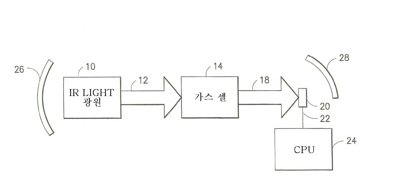
도 1은 써모파일 검출기 시스템의 개요도를 나타낸 것이다. 1 shows a schematic diagram of a thermopile detector system.
도 2는 IR 셀 시그널(curve A) 및 아르신(arsine) 농도를 나타낸 그래프로써, FT-IR 분광기가 장착된 써모파일 검출기에서 시간(초)에 따른 스크러버 테스트 컬럼의 배기관에서의 아르신 방출(breakthrough)을 모니터링 한 것이다.FIG. 2 is a graph showing IR cell signal (curve A) and arsine concentrations, showing the release of arsine in the exhaust pipe of a scrubber test column over time in a thermopile detector equipped with an FT-IR spectrometer. breakthrough).
도 3은 가스 상 모니터링을 위한 써모파일 검출기 및 반도체 공정 툴과, 제외 유닛과 관련된 공정 스트림의 조절을 이용하는 반도체 공정 설비를 개략적으로 도시한 것이다. FIG. 3 schematically illustrates a semiconductor process facility utilizing a thermopile detector and semiconductor process tool for gas phase monitoring and control of the process stream associated with the exclusion unit.
도 4는 서로 다른 트리메틸 실란의 농도에 따른 써모파일 검출기 시스템의 응답을 나타낸 그래프이다. Figure 4 is a graph showing the response of the thermopile detector system according to the concentration of different trimethyl silane.
도 5는 도 4의 내용에 따른 트리메틸 실란의 보정 곡선을 나타내는 그래프이다.
5 is a graph showing a calibration curve of trimethyl silane according to the content of FIG. 4.
발명의 요약Summary of the Invention
본 발명은 반도체 공정 모니터링 및 조절용 적외선 써모파일 시스템, 및 상기 공정에 영향을 미치거나 미치지 않는 조건을 감지하는 적외선 써모파일을 사용하는 반도체 공정의 모니터링 및 조절 방법에 관한 것이다.The present invention relates to an infrared thermopile system for semiconductor process monitoring and regulation, and to a method for monitoring and regulating semiconductor processes using infrared thermopile for detecting conditions that do not affect or affect the process.
또한, 본 발명은 공정 가스의 흐름을 위한 회로를 포함하는 반도체 공정 시스템에 관한 것이다. 상기 시스템은 다음을 포함한다: The invention also relates to a semiconductor processing system comprising a circuit for the flow of process gas. The system includes:
공정 가스을 위한 가스 샘플링 영역;A gas sampling region for the process gas;
상기 가스 샘플링 영역을 통해서 적외선을 투과하기 위하여 구성되고 배열되는 적외선 광원;An infrared light source constructed and arranged to transmit infrared light through the gas sampling region;
상기 가스 샘플링 영역을 통해서 투과된 적외선을 감지하고, 공정 가스 성분의 농도에 상응하는 적외선 출력 시그널을 발생시키기 위하여 구성되고 배열되는 써모파일 검출기; 및 A thermopile detector configured and arranged to sense infrared light transmitted through the gas sampling region and to generate an infrared output signal corresponding to the concentration of the process gas component; And
상기 써모파일 검출기의 출력을 수신하고, 상기 반도체 공정 시스템에 영향을 미치거나 미치지 않는 하나 또는 그 이상의 공정 조건들을 응답적으로 조절하기 위하여 배열되는 공정 조절 수단.Process control means arranged to receive an output of the thermopile detector and to responsively adjust one or more process conditions that do not affect or affect the semiconductor process system.
또한, 본 발명은 가스공정 또는 가스를 사용하는 공정을 포함하는 반도체 공정을 조절하는 방법에 관한 것으로서, 상기 방법은 써모파일 검출기를 이용하여 바람직한 가스 성분의 농도를 감지하는 것, 써모파일 검출기로부터 상기의 선택된 가스 성분의 농도를 나타내는 출력을 발생시키는 것, 및 상기 출력에 상응하여 반도체 공정에 영향을 미치거나 미치지 않는 하나 또는 그 이상의 조건을 조절하는 것을 포함한다. In addition, the present invention relates to a method for controlling a semiconductor process including a gas process or a process using a gas, the method is to detect the concentration of the desired gas component using a thermopile detector, from the thermopile detector Generating an output indicative of the concentration of the selected gas component of and adjusting one or more conditions in accordance with said output that do not affect or otherwise affect the semiconductor process.
본 발명의 다른 특징 및 구현에는 다음의 상세한 설명 및 첨부된 특허청구범위로부터 더욱 명백해질 것이다.
Other features and implementations of the present invention will become more apparent from the following detailed description and the appended claims.
발명의 상세한 설명 및 본 발명의 바람직한 구현예DETAILED DESCRIPTION OF THE INVENTION AND PREFERRED EMBODIMENTS OF THE INVENTION
본 발명은 반도체 공정 모니터링 및 조절에 유용한 적외선 써모파일 검출 시스템을 제공하며, 상기 공정에 영향을 미치거나 미치지 않는 조건을 감지하는 적외선 써모파일을 사용하는 것을 특징으로 하는 반도체 공정 모니터링 및/또는 조절 방법을 제공한다. SUMMARY OF THE INVENTION The present invention provides an infrared thermopile detection system useful for semiconductor process monitoring and control, and the method for monitoring and / or regulating semiconductor process using an infrared thermopile detecting a condition that does not affect or affect the process. To provide.
본 발명에서 사용되는 "반도체 공정"이란 용어는 반도체 제조 설비에 사용되거나 생산되는 물질의 처리 또는 공정을 포함하는 모든 작업, 실질적인 제조에 포함되지 않는 반도체 제조 설비와 관련되어 수행되는 작업뿐만 아니라, 반도체 제품의 제조에 관련된 어떠한 그리고 모든 공정과 유닛 작업을 포함하여 포괄적으로 구성되는 것을 의미한다 (예를들어, 공정 장비의 상태, 작업을 위한 준비 단계에서의 화학적 운반 라인의 세척, 공정 툴 챔버(chamber)의 에칭 클리닝, 반도체 제조 설비에 의해 생산되는 폐기물의 유독하고 위험한 가스의 제거 등을 포함한다.). The term " semiconductor process " as used herein refers to all operations involving the processing or processing of materials used or produced in semiconductor manufacturing equipment, as well as operations performed in connection with semiconductor manufacturing equipment not included in substantial manufacturing. Means a comprehensive configuration, including any and all process and unit operations involved in the manufacture of the product (eg, the condition of the process equipment, cleaning of the chemical delivery line in preparation for the operation, process tool chamber) Etch cleaning), removal of toxic and hazardous gases from waste produced by semiconductor manufacturing facilities, etc.).
본 발명의 적외선 검출 시스템의 작동은 대부분의 적외선 에너지를 흡수하는 분자들이 불연속적인 에너지 레벨에서 적외선을 흡수한다는 사실에 기초한 것이며, 기체, 액체 및 고체 조성이 광범위한 파장의 적외선에 노출되었을 경우, 상기 조성들 중 적외선 에너지를 흡수하는 성분은 매우 특정한 파장에서 IR 빛을 흡수할 것이다. 이러한 현상은 IR-흡수 성분을 가지는 그리고 가지지 않는 에너지 스펙트럼의 비교를 가능하게 하며, 어떠한 조성에서 특정 물질을 확인하는 데 사용될 수 있는 패턴을 가지는 흡수 프로파일(profile)을 획득할 수 있도록 한다. 이에 더하여, 어떠한 조성에서의 물질의 농도를 상기 물질에 의해 흡수되는 빛의 양에 의해 직접적으로 측정할 수 있다. The operation of the infrared detection system of the present invention is based on the fact that most of the molecules that absorb infrared energy absorb infrared rays at discrete energy levels, and when gas, liquid and solid compositions are exposed to a wide range of infrared radiation, the composition Of these components absorb infrared energy at very specific wavelengths. Will absorb light. This phenomenon allows for comparison of energy spectra with and without IR-absorbing components, and to obtain an absorption profile with a pattern that can be used to identify a particular material in any composition. In addition, the concentration of a substance in any composition can be measured directly by the amount of light absorbed by the substance.
초기 IR 분석기들은 회절격자 기술 또는 IR 방사선을 각각의 파장으로 분산시키는 프리즘을 사용하는 분광기들이었다. 이때, 각각의 에너지들은 이동 슬릿 어퍼쳐에 의해 가스 셀속으로 도입되며, 가스 셀을 통과하여 선택된 파장을 갖는 방사선이 검출된다. 상기 분산성의 IR 분석기는 IR 에너지 레벨을 가지는 슬릿 어퍼쳐(slit aperture) 포지션과 검출기로부터의 시그널과의 상관관계를 가지는 전기적 공정 수단에 사용될 수 있으며, 에너지와 흡광도의 관계를 산출하는데 이용될 수 있다. 상기 분광 분광기의 주된 단점은 고장나기 쉬운 이동 부품의 사용, 다수의 부품의 사용으로 인한 높은 비용, 및 분산 분광기의 특징적인 작동 중의 하나인 느린 안정화 속도(collection rate) 등이다. 상기 분산 분광기와 비슷한 FT-IR(fourier transform IR) 분광기는 광범위한 에너지 IR 광원을 사용한다. 초기에 재생되는 IR 빔(beam)은 두개의 빔(beam)으로 쪼개어지고 이동 반사경(moveable mirror)을 이용하여 안쪽 및 바깥상의 두개의 빔 중 하나의 빔을 방출함에 따라 간섭 패턴이 생성된다. 레이져 빔은 실시간으로 이동 반사경의 위치를 모니터링하기 위하여 사용된다. 듀얼 빔(dual beam)이 샘플에 방출된 후, 분광기기의 센서 성분은 레이져-포지션닝 빔(laser-positioning beam)과 더불어 컨볼루션된(convoluted) 적외선 파장 패턴을 전송받는다. 이때 상기 정보는 컴퓨터로 보내지고, FT 알고리즘에 의해 에너지에 대한 반사경의 변위 데이터를 에너지에 대한 흡광도의 데이터로 변환시키게 된다. 상기 FT-IR 분광기의 단점은 그들의 복잡성 및 상당한 비용에 있다. Early IR analyzers were spectroscopy using diffraction grating technology or prisms that disperse IR radiation at each wavelength. At this time, the respective energies are introduced into the gas cell by the moving slit aperture, and radiation having a selected wavelength is detected through the gas cell. The dispersible IR analyzer can be used in electrical processing means having a correlation between a slit aperture position having an IR energy level and a signal from a detector and can be used to calculate the relationship between energy and absorbance. . The main disadvantages of such spectroscopy are the use of prone to faulty moving parts, the high cost of using multiple parts, and the slow collection rate, which is one of the characteristic operations of distributed spectroscopy. Fourier transform IR (FT-IR) spectroscopy, similar to the scatter spectrometer, uses a wide range of energy IR light sources. The initially regenerated IR beam is split into two beams and an interference pattern is created by emitting one of the two beams on the inside and the outside using a moveable mirror. The laser beam is used to monitor the position of the moving reflector in real time. After the dual beam is emitted to the sample, the sensor component of the spectrometer is sent a convoluted infrared wavelength pattern along with the laser-positioning beam. At this time, the information is sent to the computer, and the FT algorithm converts the displacement data of the reflector with respect to energy into data of absorbance with respect to energy. The disadvantages of these FT-IR spectroscopy are their complexity and considerable cost.
본 발명에 실질적으로 적용되는 적외선 써모파일 검출기는 상기 분산 분광기 및 FT-IR 분광기에 비하여, (ⅰ) 낮은 비용, (ⅱ) 장치의 간단성(이동 부품이 없음), (ⅲ) 빠른 응답성 등의 많은 장점을 가지고 있다. Infrared thermopile detectors substantially applied to the present invention have (i) lower cost, (ii) device simplicity (no moving parts), (i) faster response than the dispersion spectrometer and FT-IR spectrometer. Has many advantages.
본 발명의 써모파일에 기초한 적외선 모니터링 시스템은 적외선 광원, 가스 셀(gas cell) 및 써모파일 검출기를 포함한다. 상기 가스 셀(gas cell)은 가스 샘플 모니터링 영역이며, 상기 가스 샘플 모니터링 영역은 본 발명의 광범위한 적용에 있어서 어떠한 적당한 구획을 포함할 수도 있으며, 공정의 모니터링 및 조절을 위한 조절 시그널을 생성시키는 IR-흡광도에 의해 결정되는 출력을 사용할 목적으로 가스를 통과한 IR 빛에 의해 모니터링되는 가스가 지나가는 통로 및 챔버를 포함할 수도 있다. 바람직한 적용을 위하여, 본 발명의 모니터링 시스템은 반사경 및/또는 IR 광선을 조준하고 직접적으로 전송하기 위한 렌즈를 이용할 수 있다. 써모파일 검출기는 IR 광선에 노출되었을 경우(또는 IR 스펙트럼 레짐(spectral regime)에서의 열) 낮은 전압을 발생시킨다. 상기 써모파일 검출기의 출력 시그널은 검출기에서 발생하는 방사선에 비례한다. An infrared monitoring system based on the thermopile of the present invention includes an infrared light source, a gas cell and a thermopile detector. The gas cell is a gas sample monitoring region, which may comprise any suitable compartment for a wide range of applications of the present invention, and IR- which generates a control signal for the monitoring and regulation of the process. It may also include passages and chambers through which the gas is monitored by IR light passing through the gas for the purpose of using the output determined by absorbance. For preferred applications, the monitoring system of the present invention may utilize a lens for aiming and directly transmitting a reflector and / or IR light. Thermopile detectors generate low voltages when exposed to IR light (or heat in an IR spectral regime). The output signal of the thermopile detector is proportional to the radiation generated by the detector.
바람직하게 본 발명의 써모파일 검출기는 각각의 검출기 유닛에서 구성요소들의 복합적인 배열을 가질 수 있다. 예를 들어, 듀얼 엘레먼트 검출기(dual element detector)에서, 써모파일 검출기의 구성요소들 중 하나는 실질적으로 흡광 작용이 일어나지 않는 범위(e.g., 4.00±0.02 ㎛의 파장)에서의 IR 빛을 감지하기위한 참고로써 사용될 수 있다. 두번째 써모파일 검출기의 구성요소는 관심있는 스펙트럼 범위(모니터링되는 특정 물질에 의존하는 스펙트럼 범위)에서 IR 에너지를 감지하는 필터로 코팅될 수 있다. 상기의 참고 써모파일 검출기 구성요소에 의해 생성된 전압과 써모파일 검출기 활성 구성성분에 의해 생성된 전압과의 차이는 농도 측정에 사용될 수 있다. 4개의 써모파일 구성요소가 배열된 검출기가 상업적으로 이용가능하다. 예를들어, 4-구성요소 검출기 유닛(unit)에서, 하나의 검출기 구성요소는 참고로서 적용될 수 있고, 남아있는 3개의 검출기 구성요소는 다른 스펙트럼 영역의 측정에 사용될 수 있다. Preferably the thermopile detector of the invention may have a complex arrangement of components in each detector unit. For example, in a dual element detector, one of the components of the thermopile detector is for detecting IR light in a range where substantially no light absorption occurs (eg, a wavelength of 4.00 ± 0.02 μm). Can be used as a reference. The components of the second thermopile detector may be coated with a filter that senses IR energy in the spectral range of interest (the spectral range depending on the particular material being monitored). The difference between the voltage generated by the reference thermopile detector component and the voltage generated by the thermopile detector active component can be used for concentration measurements. Detectors with four thermopile components arranged are commercially available. For example, in a four-component detector unit, one detector component can be applied as a reference and the remaining three detector components can be used for the measurement of other spectral regions.
도 1은 써모파일에 기초한 검출기 시스템의 작동을 설명하기 위한 개략도를 나타낸 것으로서, IR 램프와 같은 IR 광원(10)은 광범위한 적외선 빔(12)을 생성한다(IR 파장의 확장된 스펙트럼 범위). 상기 IR 빔(12)은 분석을 위해 모니터링되는 가스가 나타내는 내부부피(16)를 가지는 가스 셀(14)에 작용하게 된다. 상기 가스 셀은 반도체 공정 시스템에서 구획, 횡단면 영역 또는 가스 플로우 도관의 부분일 수 있다. 일반적으로, 가스 플로우의 슬립-스트림(side stream)은 가스 모니터링 작업을 위한 플로우 도관 또는 공정 툴(tool) 파이핑(piping)으로부터 인용될 수 있다.
1 shows a schematic diagram illustrating the operation of a detector system based on a thermopile, in which an
가스 셀(14)의 내부 부피(16)를 통과하고 가스들의 상호작용 후에, 횡단과 동시에 가스 셀(14)로부터 방사되는 IR 방사선은 써모파일 검출기(20)에 작용하게 된다. 써모파일 검출기 유닛은 특정 IR 파장의 방사선이 필터를 통과할 수 있도록 깊숙이 끼워진 IR 필터를 이용할 수 있으며, 그 결과로써 써모파일 검출기가 방사선 강도를 결정하고 검출기의 각 구성요소의 출력 전압을 생성할 수 있다. 도 1에 나타낸 써모파일 검출기 유닛의 전압 출력은 시그널 송신 라인(22)으로부터 중앙 공정 유닛(24)으로 통과하게 되고, 예를 들어 개인 컴퓨터, 마이크로프로세서 기기, 또는 다른 계측 수단을 들수 있는데, 여기서 검출기 구성요소에 의해 생성된 전압 시그널은 관심있는 가스 성분 각각의 출력 농도값을 산출하기 위해 연산방식으로 처리된다.After passing through the internal volume 16 of the
도 1에 나타낸 바와 같이 써모파일에 기초한 분석 시스템은 IR 방사선의 촛점을 맞추기 위한 반사경[(26) 및 (28)]을 포함한다. 상기 반사경들은 검출한계를 향상시키기 위하여 내부 부피(16)를 가로질러 적외선 빔(beam)에 1회 이상 통과시키는데 사용될 수 있다. 도 1의 적외선 광원(10)은 예를 들어, 약 2~4.6㎛파장 스펙트럼(spectrum)에서 IR 방사선을 제공하는 퍼킨엘머 IRL 715 적외선 램프와 같은 어떠한 적당한 형태일 수 있다. 이와 마찬가지로 써모파일 검출기(20) 또한 적당한 형태일 수 있으며, 바람직하게는 퍼킨 엘머 TPS 3xx 싱글 검출기, 퍼킨엘머TPS 5xx 싱글 검출기, 퍼킨엘머 2534 듀얼 검출기 또는 퍼킨엘머 4339 쿼드(quad) 검출기일 수 있다. 상기의 적외선 광원(10) 및 써모파일 검출기(20) 구성요소들은 퍼킨엘머 옵토일렉트로닉스사(Wiesbaden, Germany)로부터 상업적으로 이용될 수 있다.
As shown in FIG. 1, a thermopile based analysis system includes
본 발명의 바람직한 구현예로써 써모파일 검출기 구성요소들은 10-40 밀리초(millisecond) 범위의 반응시간을 가진다. 본 발명에 적용된 써모파일 검출기 유닛은 측정된 적외선 빛을 수집하기 위한 검출기 흡수영역, 흡수영역 아래에 위치한 열적 구성요소를 효과적으로 배열시킬 수 있으며, 그리하여 흡수영역에서의 적외선 빛의 갑작스런 발생은 상기 흡수영역을 가열하고 출력 리드에서 갑작스럽게 발생한 방사선 전력의 직접적인 측정에 의한 DC 전압을 발생시키게 된다. 상기 써모파일 검출기 유닛은 써모파일 검출기 구성요소 정면에 위치한 가스-특이적 적외선 밴드 패스 필터(gas-specific infrared radiation band pass filter)에 유익하게 적용될 수 있으며, 그리하여 상기 써모파일에 의하여 생성된 출력 전압의 감소는 이에 상응하는 가스에 의한 적외선 흡수량과 직접적으로 관련된다. 상기 써모파일 검출기 유닛은 참고 흡수 영역(여과되지 않음) 및 가스-여과된 흡수 영역을 포함하며, 반도체 가스 또는 관심있는 가스 성분(예를 들어, 아르신, 포스핀, 게르만, 스티빈, 디스티빈, 실란, 치환된 실란, 염소, 브롬, 유기금속 선구 증기 등)을 감지하기 위한 가스-특이적 래더 필터(latter filter)를 가지는 다수의 흡수영역을 포함할 수 있다.In a preferred embodiment of the present invention, the thermopile detector components have a response time in the range of 10-40 milliseconds. The thermopile detector unit applied to the present invention can effectively arrange a detector absorbing area for collecting measured infrared light and a thermal component located below the absorbing area, so that sudden generation of infrared light in the absorbing area is prevented. And generate DC voltage by direct measurement of the radiation power suddenly generated at the output lead. The thermopile detector unit can be advantageously applied to a gas-specific infrared radiation band pass filter located in front of the thermopile detector component, thereby reducing the output voltage generated by the thermopile. The reduction is directly related to the amount of infrared absorption by the corresponding gas. The thermopile detector unit comprises a reference absorbing region (not filtered) and a gas-filtered absorbing region and comprises a semiconductor gas or a gas component of interest (e.g. arsine, phosphine, germane, stibin, distibin). , Silane, substituted silane, chlorine, bromine, organometallic precursor vapor, etc.) may comprise a plurality of absorption zones having a gas-specific ladder filter.
본 발명에 따른 써모파일 IR 검출기 유닛은 하기에서 더욱 상세히 설명되는 반도체 공정 적용에서의 공정 조절에 유용하게 적용될 수 있다. The thermopile IR detector unit according to the invention can be usefully applied for process control in semiconductor process applications, which will be described in more detail below.
본 발명의 일 구현예로써, 써모파일 IR 검출기 유닛은 툴 챔버 및/또는 플로우 회로의 내부로 적당한 농도의 물질이 운반되었는지 확인하기 위한 가스 운반 모니터링 유닛, 예를 들어, 반도체 툴의 가스 운반 라인에 설치되는 인-라인 모니터, 로 유용하게 적용될 수 있다. In one embodiment of the invention, the thermopile IR detector unit is provided in a gas delivery monitoring unit, for example in a gas delivery line of a semiconductor tool, to verify that a suitable concentration of material has been delivered into the tool chamber and / or the flow circuit. It may be usefully applied to the line monitor-in to be installed.
상기 적용에 있어서, 써모파일 검출기 유닛의 고유한 안정성은 정확한 농도 의 측정을 쉽게할 수 있다. 상기 가스 운반의 감지 및 조절에 써모파일 검출기의 사용은 툴로의 공급 가스의 미터제 운반에 사용되는 매스 플로우 조절기를 조정하는 필요를 최소화할 수 있다. 더욱이 써모파일 검출기 유닛에 의해 생성된 시그널은 피드백 제어 배열(feedback control arragements), 예를 들어, 농도, 부피당 유속, 반응용매를 일정하게 유지하기 위하여 써모파일 검출기 유닛으로부터 매스 플로우 조절기로의 운반 속도를 증가시키거나 또는 감소시키는 피드백이 반도체 공정에서 실행될 수 있도록 한다.In this application, the inherent stability of the thermopile detector unit can facilitate the measurement of accurate concentrations. The use of a thermopile detector to detect and regulate the gas delivery can minimize the need to adjust the mass flow regulator used for the metric delivery of feed gas to the tool. Furthermore, the signal generated by the thermopile detector unit can be used to control the rate of transport from the thermopile detector unit to the mass flow regulator to maintain a constant feedback control arrangement, e.g. concentration, flow rate per volume, reaction solvent. Increasing or decreasing feedback may be implemented in the semiconductor process.
본 발명의 다른 구현예로써, 써모파일 검출기 유닛은 반도체 제조 공정 또는 다른 산업 공정에서 생산되는 폐기물을 처리하기 위한 제외 시스템(abatement system)의 제외 툴 조절기로 이용될 수 있다. 상기 목적을 위하여, 써모파일 검출기 유닛은 처리하기 위한 폐기물이 유입되는 제외 기기의 유입구에 설치될 수 있다. 상기 공정에서, 써모파일 검출기 유닛은 온-스트림 작업 상태에서 페기물을 생산하는 업스트림 툴이 활발히 작동하는지의 여부 또는 업스트림 툴이 비-폐기물-생산 상태인지의 여부, 예를 들어, 세정 또는 클리닝 작업을 수행하고 있는지를 감지하는데 사용될 수 있다.In another embodiment of the present invention, the thermopile detector unit may be used as an exclusion tool regulator in an exclusion system for treating waste produced in semiconductor manufacturing processes or other industrial processes. For this purpose, the thermopile detector unit can be installed at the inlet of the exclusion apparatus into which waste for processing is introduced. In the process, the thermopile detector unit performs an active operation of the upstream tool producing waste in the on-stream working state or whether the upstream tool is in a non-waste-producing state, for example a cleaning or cleaning operation. Can be used to detect if it is performing.
써모파일 검출기 유닛은 습식 스크러버 또는 건식 스크러버와 같은 폐기물 스크러버의 제외 툴 조절기로 유용하게 사용될 수 있으며, 상기 써모파일 검출기 유닛의 적용으로 인하여 스크러버를 "스마트" 스크러버로 변모시킬 수 있고, 공급 원의 유지(낮은 소비성)로 인하여 스크러버의 효율을 향상시킬 수 있다.The thermopile detector unit can be usefully used as an exclusion tool regulator for waste scrubbers such as wet scrubbers or dry scrubbers, and the application of the thermopile detector unit can transform the scrubber into a “smart” scrubber and maintain the source of supply. Due to (low consumption), the efficiency of the scrubber can be improved.
또 다른 구현예로써, 본 발명의 써모파일 검출기 유닛은 업스트림 반도체 공정 툴로부터 폐기물 제외 스크러버로 배출되는 폐기물의 형태에 따른 제외 장치 및/또는 제외 처리 방법의 변화를 용이하게 적용하기 위한 폐기물 처리 공정에 유용하게 이용될 수 있다. 이를테면, 써모파일 검출기 유닛이 증착물(예를들면, 실란, low-k 물질)을 검출할 경우, 폐기물 가스 스트림은 모니터링 및 제어 시스템에 의해 증착공정(열적 산화 유닛)에서의 폐기물을 배제하기 위한 적당한 다른 제외 툴로 보내질 수 있다. 상기 써모파일 검출기 유닛이 증착물질을 감지하지 못할 경우, 툴(예를 들어, 업스트림 증기 증착 챔버)은 클리닝 단계를 거치게 되며, 이때 가스 스트림은 클리닝 단계에서의 폐기물을 배제하기 위한 "가장 적당한 툴(예를 들어, 습식 스크러버)"로 보내진다.In another embodiment, the thermopile detector unit of the present invention is adapted to a waste treatment process for easily applying changes in the exclusion apparatus and / or exclusion treatment method according to the type of waste discharged from the upstream semiconductor process tool to the waste exclusion scrubber. It can be usefully used. For example, if the thermopile detector unit detects deposits (eg, silanes, low-k materials), the waste gas stream is suitable for excluding waste in the deposition process (thermal oxidation unit) by a monitoring and control system. Can be sent to other exclusion tools. If the thermopile detector unit does not detect deposits, the tool (e.g., upstream vapor deposition chamber) is subjected to a cleaning step, where the gas stream is a "most suitable tool" to exclude waste during the cleaning step. For example, "wet scrubber".
또한 다른 구현예로써, 써모파일 검출기 유닛은 반도체 공정 챔버의 다운스트림(downstream)에 설치되는 종말점 검출기로 유용하게 이용될 수 있다. 상기 공정에서, 분석기는 공정 챔버로부터 배출되는 특정성분의 농도를 시간에 따라 감지하는 인-라인 모니터로 사용될 수 있다. 공정 챔버로부터 배출되는 폐기물의 농도 변화는 툴 오퍼레이터(operator) 및/또는 기기의 작동을 중단하거나 또는 세정, 클리닝과 같은 전처리 공정을 개시하는 자동화 공정 조절 장치로 보내지는 종점 시그널을 발생시키기 위하여 사용될 수 있다. In another embodiment, the thermopile detector unit may be usefully used as an endpoint detector installed downstream of the semiconductor process chamber. In this process, the analyzer can be used as an in-line monitor that detects the concentration of a particular component exiting the process chamber over time. Changes in the concentration of waste discharged from the process chamber can be used to generate an endpoint signal sent to an automated process control device that shuts down tool operators and / or equipment or initiates pretreatment processes such as cleaning and cleaning. have.
도 2는 건식 스크러버 테스트 컬럼의 배기관에서 아르신의 방출을 모니터링하기 위하여 FT-IR 분광기 및 써모파일 검출기 유닛을 교대로 사용하여 수집한 측 정치들을 나타낸 것이다. 아르신 스트림은 비소 도핑 공정에서 반도체 기기 구조에 의해 생성되거나 또는 에피택셜 성장 공정에서 갈륨 비화물에 의해 생성되는 As-코팅된 폐기물의 시뮬레이션을 의미한다.Figure 2 shows measurements collected using alternating FT-IR spectroscopy and thermopile detector units to monitor the release of arsine in the exhaust pipe of a dry scrubber test column. Arsine stream refers to the simulation of As-coated wastes produced by semiconductor device structures in an arsenic doping process or by gallium arsenide in an epitaxial growth process.
도 2에 나타낸 바와 같이, 써모파일 검출기 유닛의 응답(curve A)은 FT-IR 분광기 시그널(curve B)보다 빠르므로, 써모파일 검출기 유닛은 농도 변화의 경향을 포착하는 것이 가능하다. As shown in Fig. 2, since the response curve A of the thermopile detector unit is faster than the FT-IR spectrometer signal curve B, the thermopile detector unit can capture the tendency of the concentration change.
도 3은 유독하거나 위험한 폐기물의 성분을 배제시키기 위한 제외 유닛(104)과 반도체 공정 툴(102)을 포함하는 반도체 공정 시스템(100)의 개요도를 나타낸 것이다. 상기 시스템은 하기에 좀더 상세히 서술되는 바와 같이, 다양한 써모파일 검출기 유닛을 이용한 공정 모니터링 및 조절을 위한 중앙 공정 유닛(CPU)(110)을 포함할 수 있다.3 shows a schematic diagram of a
반도체 공정 툴(102)은 반응원료 공급원(108)으로부터 반응원료를 공급받기 위하여 배열되어 진다. 예로써, 반도체 공정 툴(102)은 반응원료인 실란 가스가 있는 에피택셜 성장 챔버를 포함하거나, 반도체 공정 툴(102)은 반응원료 공급원(108)으로부터 유기금속 전조체를 공급받는 CVD(chemical vapor deposition) 챔버를 포함하거나, 또는 반도체 제조 설비에서의 어떠한 다른 공정 유닛을 포함할 수 있다. The
반응원료 공급원(108)으로부터의 반응원료는 공급 라인(114)에서 반도체 공정 툴(102)로 흐른다. 공급 라인(114)은 매스 플로우 조절기와 작동관계에 있는 매스 플로우 조절기 셋 포인트 조정 유닛(138)이 장착된 매스 플로우 조절기(112)를 포함한다. 써모파일 검출기 유닛(116)은 공급 라인(114)에 인-라인 방식으로 설치되며, 상기 공급 라인(114)에서 반도체 공정 툴로 흘러들어가는 가스 상의 반응물을 검출하기 위하여 배열된다. 써모파일 기기(116)에 의해 생성되는 가스 농도 시그널은 시그널 전송 라인(142)에서 CPU(110)로 전송된다. 상기 CPU(110)는 차례로 조절 관계에 배열될 수 있고, 매스 플로우 조절기 셋 포인트 조정 유닛(138)으로의 조절 시그널 라인(140)의 수단들에 의해 배열될 수 있으며, 상기 매스 플로우 조절기 셋 포인트 조정 유닛(138)은 매스 플로우 조절기(112)의 셋 포인트를 조절한다.Reactant from the
이러한 방식에 있어서, 매스 플로우 조절기의 셋 포인트는 조정 유닛(138)에 의해 매스 플로우 조절기의 셋 포인트를 조정하기 위하여 써모파일 검출기(116)에 의해 감지되는 농도에 따라 모듈될 수 있으며, 그리하여 매스 플로우 조절기(112)는 반도체 공정 툴에서 반응원료의 정밀한 셋 포인트 플로우를 제공할 수 있다.In this manner, the set point of the mass flow regulator can be modularized according to the concentration sensed by the
도 3의 시스템에서, 반도체 공정 툴(102)은 폐기물 배출 라인(118)에서 고유한 특성을 가지는 처리된 폐기물을 생성시키기 위한 처리에 사용되는 제외 유닛(104)으로부터 흘려보내지는 폐기물을 생성하게 되며, 상기 폐기물은 제외 유닛124)으로부터 제외 유닛 배출 라인(124)으로 방출된다. In the system of FIG. 3, the
써모파일 검출기 유닛(120)에 의해 감지되는 폐기물 배출 라인(118)의 폐기물 스트림에서의 선택된 성분(들)에 응답하여, CPU(110)는 셋 포인트 조절 유닛(138)을 모듈함에 의해 매스 플로우 조절기(112)의 셋 포인트를 조정하게 된다. 일반적으로, 써모파일 검출기 유닛(120)에 의해 감지되는 폐기물 배출 스트림에서의 감지된 농도에 응답하는 CPU(110)는 공급 라인(114)의 플로우 조절 밸브(도면에 나 타내지 않음)의 폐쇄 및/또는 반도체 공정 툴(102)이 포함되는 조정 또는 종결 단계에서의 다른 작동들에 영향을 미침에 의해 반응원료의 흐름을 종결시킬 수 있다.In response to the selected component (s) in the waste stream of the
예를 들어, 써모파일 검출기 유닛(120)에 의해 감지되는 폐기물 가스는 활성 공정 모드에서 클리닝 모드, 또는 첫번째 활성 공정 단계에서 연속적인 공정단계로의 반도체 공정 툴(102)의 효과 전환에 적용될 수 있다. 구체적인 예로써, 써모파일 검출기 유닛(120)에 의해 감지되는 배출 라인(118)에서의 폐기물 스트림의 관심성분의 농도는 시그널 송신 라인(154)에서 CPU(110)로 전송되는 농도 시그널을 생성시키는데 이용될 수 있다. 상기 농도 시그널은 활성 공정 단계가 만족스럽게 완료되었는지를 표시할 수 있다. 이때 상술한 바와 같이, 상기 CPU(110)는 반응원료 공급원(108)으로부터 툴로의 반응원료의 흐름을 종결시키게 된다. 동시에 상기 CPU는 제어 시그널을 제어 시그널 송신 라인(152)에서 밸브 조절기(150)로 전송한다. 상기 밸브 조절기(150)는 세정 가스 공급원(144)에 연결된 세정 가스 공급 라인(146)의 플로우 조절 밸브(148)와 상호조절 관계를 가지고 연결되어 있다. CPU(110)로부터의 조절 시그널은 밸브 조절기(150)에 작용하게 되며, 상기 밸브 조절기(150)는 차례로 밸브(148)를 개봉하고, 세정 가스가 반도체 공정 툴(102)로 흘러들어 가도록 한다.For example, the waste gas sensed by the
이러한 방식에서, 공정 툴은 효과적으로 반응원료 가스들을 세정하며, 그리고 이에 수반하는 활성 공정을 준비시키거나, 또는 일반적으로 활성(on-stream)공정이 수반되기 이전 단계인 클리닝 단계를 준비시키게 된다. 반응원료 잔류물의 제거, 부산물의 분해 등을 위하여 세정 가스가 충분히 공정 툴을 통과하여 흐를 경 우, 써모파일 검출기 유닛(120)에 의해 감지되는 농도 및 시그널 송신 라인(154)에서 CPU(110)로의 농도 시그널의 송신이 일치되어 나타남에 따라, CPU는 밸브(148)를 폐쇄하고 공정 툴로의 세정 가스의 흐름을 종식시키기 위하여 밸브 조절기(150)를 작동시키게 된다.In this way, the process tool effectively cleans the reactant gases and prepares the accompanying active process, or generally prepares the cleaning step, which is before the on-stream process. If the cleaning gas flows sufficiently through the process tool for removal of reactant residues, decomposition of by-products, etc., the concentration detected by the
반도체 공정 툴(102)의 가스 공급 라인(114)에 써모파일 검출기 유닛(116)을 설치하는 대신에, 또는 이에 더하여, 시스템은 반도체 공정 툴(102)를 모니터링하고 제어하기 위하여 써모파일 검출기 유닛(120)을 유출수 방전 라인(118)에 적용할 수 있다. Instead of, or in addition to installing, the
추가로 또는 선택적으로, 제외 유닛(104)의 써모파일 검출기 유닛(120) 업스트림은 제외 유닛(104)을 모니터링하고 제어하기 위하여 구성되고 배열될 수 있다.Additionally or alternatively, the
도 3에 나타낸 바와 같이 제외 유닛(104)은 다양한 형태일 수 있으며, 다중 제외 처리 단계 및 예를 들어 습식 스크러버, 건식 스크러버, 열적 산화 유닛, 촉매에 의한 산화 유닛, 화학적 흡착 유닛, 물리적 흡착 시스템 등으로 구성되는 공정 유닛을 포함할 수 있다. As shown in FIG. 3, the
일 실시예로써, 도 3은 습식 세정에 요구되는 방전 라인(118) 내의 반도체 공정 툴(102)로부터 유출수를 방출하기 위한 수단인, 습식 세정 유닛을 포함하는 제외 유닛(104)을 나타낸 것이다. 습식 세정은 적당한 액체 세정 물질, 예를 들어, 세정 물질 소스(106)에서 공급되어지고 세정 물질 공급 라인(162)에서 제외 유닛(104)으로 흘러들어가는 물, 산성 수용액, 염기성 수용액 등을 이용하여 스크러버 제외 유닛(104)에서 수행된다.
As an example, FIG. 3 shows an
상기 라인(162)에서 세정 물질의 유속은 밸브 조절기(158)에 연결되어 작동하는 플로우 조절 밸브(160)에 의해 조절되며, CPU(110)로부터 시그널 송신 라인(156)을 통하여 전송된 조절 시그널에 의해 조정된다.The flow rate of the cleaning material in
그러므로, 써모파일 검출기 유닛(120)은 제외 유닛(104)에서 배제되는 성분의 농도 감지 및 시그널 송신 라인(154)에서 상기 농도에 상응하는 시그널을 CPU(110)에 전송하기 위해 유용하게 배열될 수 있다. 폐기물 스트림에서 배제되는 성분의 농도를 표시하는 상기 시그널에 응답하여, CPU(110)는 조절 시그널 송신 라인(156)에서 밸브 조절기(158)로 조절 시그널을 송신하며, 상기 CPU는 폐기물과 접촉할 수 있도록 바람직한 양의 세정 물질이 제외 유닛(104)으로 흐르도록 플로우 조절 밸브(160)의 조절점을 모듈함으로써, 폐기물 스트림에서의 관심있는 세정 성분을 제어하게 된다.Therefore, the
따라서, 폐기물 스트림에서 써모파일 검출기 유닛(120)에 의해 감지되는 상대적으로 낮은 세정 성분의 농도는 CPU(110)가 제외 유닛(104)으로의 세정물질의 흐름을 감소시키기 위하여 밸브 조절기(158)를 작동시키는 원인이 되며, 이로써, 세정 물질은 세정 성분이 제거될 수 있을 정도로 충분히 적당한 양 및 속도로 공급된다. 이때, 세정 성분을 포함하고 있는 세정 물질은 제외 유닛(104)으로부터 세정 물질 방출 라인(130)으로 배출된다.Thus, the relatively low concentration of cleaning component detected by the
유사한 방식으로, 제외 유닛(104)으로 부터 폐기물 방출 라인(124)으로 배출되는 처리된 폐기물은 써모파일 검출기 유닛(124)에 의해 모니터링될 수 있으며, 이에 해당하는 농도 시그널이 시그널 송신 라인(164)에서 CPU(110)로 전송된다. 그 결과 CPU(110)는, 상술한 바와 같이, 세정 물질의 유속을 증가시키거나 유지하거나 또는 감소시키기 위하여, 필요에 따라서 스크러버 제외 유닛(104)으로부터 방출 라인(124)으로 최종 방출되는 미리 결정된 낮은 세정 성분의 수준에 도달하기 위하여, 밸브 조절기(158)을 통하여 플로우 조절 밸브(160)를 조정함으로써 감지된 농도에 반응하게 된다. 예를 들어 이러한 미리 결정된 낮은 세정 성분의 수준은 써모파일 검출기 유닛(126)의 검출 한계보다 낮은 농도일 수 있다.In a similar manner, the treated waste discharged from the
바람직한 세정 성분의 제거 범위를 유지하기 위하여 세정 물질의 유속을 모듈하는 것에 더하여, 써모파일 검출기에 의해 감지된 세정 성분의 농도는 시그널 송신 라인(164)에서 CPU(110)로 전송될 수 있고, 이에 상응하여 방출 라인(124)으로부터 라인(128) 내의 제외 유닛(104)의 유입구로 폐기물이 재순환하도록 조정할 수 있다.In addition to modularizing the flow rate of the cleaning material to maintain the desired removal range of the cleaning component, the concentration of cleaning component sensed by the thermopile detector can be transmitted from the
상기 라인(128)은 방출 라인(124)에 배치된 3-웨이 밸브(132)와 연결되어 있다. 밸브 조절기(134)는 3-웨이 밸브(132)와 역학적으로 연결되어 있다. 밸브 조절기(134)는 컨트롤 시그널 송신 라인(136)에 의해 CPU(110)에 단단히 고정되어 있다. 상기와 같은 배열로 인해, 제외 유닛(104)으로부터 폐기물에서의 세정 성분의 농도가 써모파일 검출기 유닛(126)에 의해 감지되며, 감지된 농도 시그널은 시그널 송신 라인(164)에 의해 CPU(110)로 전송된다. CPU(110)는 이에 응답하여 시그널 송신 라인(136)에서 3-웨이 밸브(132)와 연결된 밸브 조절기(134)로 조절 시그널을 전송하게 되며, 이에 의하여 밸브(132)는 방출 라인(124)으로부터 처리된 유출수가 제외 유닛(104)으로 재도입될 수 있도록 라인(128)에서 라인(118)으로 재순환하도 록 조정된다.The
상기와 같은 방식으로, 제외 유닛(104)에서의 세정 성분의 제거 효율을 최대화할 수 있도록 세정 물질의 유속 뿐만 아니라, 순환 속도도 조절될 수 있다.In this manner, the circulation rate as well as the flow rate of the cleaning material may be adjusted to maximize the removal efficiency of the cleaning component in the
써모파일 검출기 유닛이 가스 농도를 모니터링하며, 이에 반응하여 유체의 유속을 제어하는 반도체 공정 시설 및/또는 다른 공정 조건 및/또는 반도체 공정 조작상의 여러 양상에 다양하게 적용될 수 있다는 것은 전술한 도 3의 구현예에서의 결론에서 명백히 알 수 있으며, 이에 의하여 공정효율을 최대화할 수 있고, 공정 반응의 요구조건을 최소화할 수 있으며, 그리고 써모파일 검출기를 이용한 모니터링 및 제어 수단의 결핍으로 인한 반도체 제조 설비와 관련된 제품의 일관성을 좀더 효과적으로 달성할 수 있다.The thermopile detector unit monitors gas concentration and can be variously applied to various aspects of semiconductor process facilities and / or other process conditions and / or semiconductor process operations in response to controlling the flow rate of fluid. It can be clearly seen from the conclusions in the embodiment, thereby maximizing the process efficiency, minimizing the requirements of the process reaction, and the lack of monitoring and control means using thermopile detectors and The consistency of the products involved can be achieved more effectively.
또한, 도 3의 구현예는 일반적으로 관심있는 단일 기체 성분(모니터링된 기체 종과 같은)에 관하여 기술하고 있을지라도, 다중성분 공정 스트림에서 다양한 기체 성분들의 농도를 감지하는 기능을 가지는 본 발명의 다중-성분 써모파일 검출기가 유용하게 적용될 수 있다는 것은 상기 본 명세서에서 서술한 바로부터 주지될 수 있을 것이다.In addition, although the embodiment of FIG. 3 generally describes a single gas component (such as a monitored gas species) of interest, the multiple of the present invention has the ability to sense the concentration of various gas components in a multicomponent process stream. It can be noted from the description herein that the component thermopile detector can be usefully applied.
또한, 본 발명은 참고로써 단일 반도체 공정 툴에 관하여 서술하고 있을 지라도, 통상적인 반도체 공정 시설이 다중 툴 및 공정 시스템 성분을 포함한다는 것은 인정될 것이므로, 써모파일 검출기 유닛은 반도체 공정의 다양한 작업, 예를 들어 공정 시스템 플로우 회로의 특정 챔버 또는 영역에 다중적으로 동시에 이용될 수 있을 것이며, IR 써모파일 검출기 유닛은 하나 또는 그 이상의 컴퓨터, 공정, 싸이클-타임 프로그램 컨트롤러 등을 포함하는 조절 회로와 함께 구성될 수 있을 것이다. 또한, 전력 출력 시그널을 가지는 써모파일 검출기는 특정 작업에서 필요로 하는 공정 모니터링 및 제어 기능을 유효하게 실시하기 위하여 다른 시그널 발생기 그리고 송신/제어 기기 및 인터페이스에 유용하게 이용될 수 있을 것이다.In addition, although the present invention describes with reference to a single semiconductor process tool, it will be appreciated that a conventional semiconductor process facility includes multiple tools and process system components, so that the thermopile detector unit may be used for various operations, e. For example, it may be used simultaneously in multiple chambers or regions of a process system flow circuit, and the IR thermopile detector unit may be configured with control circuits including one or more computers, processes, cycle-time program controllers, and the like. Could be. In addition, thermopile detectors with power output signals may be useful in other signal generators and transmission / control devices and interfaces in order to effectively implement the process monitoring and control functions required for a particular task.
예를 들어, 써모파일 검출기 출력 시그널은 통합된 무선 네트워크 상에서 모니텅링 및 제어의 목적으로 라디오 주파수 수신기로 전송될 수 있도록 라디오 주파수 트랜스폰더에 의해 송신되는 라디오 주파수 시그널로 전환될 수 있을 것이다.For example, the thermopile detector output signal may be converted to a radio frequency signal transmitted by a radio frequency transponder for transmission to a radio frequency receiver for monitoring and control purposes on an integrated wireless network.
써모파일 검출기의 전력에 기초한 출력은 다른 시그널 형태로 전환될 수 있거나, 또는 중앙 공정 유닛 또는 다른 컴퓨터의 조작 또는 제어 수단과의 무선 통신을 위해 심지어는 적외선 조절 시그널로 재전환될 수도 있다.The output based on the power of the thermopile detector may be converted into other signal forms or may be converted back to an infrared conditioning signal for wireless communication with the control or control means of a central processing unit or other computer.
본 발명은 하기의 실시예에 의해 좀더 상세히 기술되나, 이에 의해 제한되지는 않으며, 다만 하기의 실시예는 참고로써 인용된다.
The invention is described in more detail by the following examples, which are not intended to be limiting, but the following examples are incorporated by reference.
실시예Example
트리메틸 실란을 사용하는 써모파일 검출기 시스템Thermopile Detector System Using Trimethyl Silane
도 4는 서로 다른 트리메틸 실란의 농도에 따른 써모파일 검출기의 응답을 나타낸 것이다. 트리메틸 실란은 반도체 공정에서 낮은-k 전조체(precursor)로 사용됨으로써 써모파일에 기초한 공정 모니터링의 적용을 위해 선택된 물질이다. 이러한 특정 시스템은 듀얼 센서 써모파일 검출기를 포함한다. 이러한 활성 원소는 메틸기(약 3000㎝-1)를 제외한 모든 IR 빛을 여과한다. 두 번째 필터는 약 2500㎝-1 근처의 좁은 밴드를 측정한다. 도 4에서 "TP 비율"로 표지된 곡선은 활성 원소의 감응(response)을 표준 원소에 의해 생성된 시그널로 나눈 값을 나타낸다. "활성"으로 표지된 곡선은 오직 활성 검출기 원소에 의해 생성된 전력에 상응하는 값을 나타낸 것이다. 도 4는 또한 모니터링 시스템의 안정성 및 재현성을 나타내고 있다.Figure 4 shows the response of the thermopile detector according to the concentration of different trimethyl silane. Trimethyl silane is the material of choice for the application of thermopile based process monitoring by being used as a low-k precursor in semiconductor processing. This particular system includes a dual sensor thermopile detector. This active element filters out all IR light except for the methyl group (about 3000 cm −1 ). The second filter measures a narrow band near about 2500 cm -1 . The curve labeled “TP ratio” in FIG. 4 represents the response of the active element divided by the signal produced by the standard element. The curve labeled “Active” only shows values corresponding to the power generated by the active detector element. 4 also shows the stability and reproducibility of the monitoring system.
도 5는 트리메틸 실란의 보정 곡선을 나타낸 것으로서, 도 4의 내용에 기초한 것이다. 도 4와 비슷하게, 하나의 보정 곡성은 활성 및 표준 시그널과의 비율을 나타낸 것이고, 반면 다른 곡선은 활성 검출기 원소에 의해 생성된 시그널을 나타낸 것이다. 상기 두 곡선들은 0.999 보다 큰 상관 계수를 갖는 2차 다항식에 따라 그려진 것들이다. 상기 보정 곡선에 근거하여, 100만 분의 500(ppm)이라는 검출 한계가 추정된다.FIG. 5 shows a calibration curve of trimethyl silane, based on the contents of FIG. 4. Similar to FIG. 4, one calibration curve represents the ratio with the active and standard signals, while the other curve shows the signal generated by the active detector element. The two curves are drawn according to a second order polynomial with a correlation coefficient greater than 0.999. Based on the correction curve, a detection limit of 500 parts per million (ppm) is estimated.
본 발명이 참고로써 서술된 구현예 및 특징들에 의해 다양하게 개시되어 있을지라도, 본 발명에 기재된 구현예 및 특징들은 본 발명을 제한하고자 함이 아니며, 다른 변형, 변경 및 그 외의 구현예들이 본 발명의 기술분야에서의 당업자에 의해 제시될 수 있다. 그러므로 본 발명은 다음의 특허청구범위에 따라 광범위하게 구성된다.Although the invention has been disclosed in various ways by the embodiments and features described by reference, the embodiments and features described herein are not intended to limit the invention, and other variations, modifications, and other embodiments are shown herein. It can be presented by those skilled in the art. Therefore, the present invention is broadly constructed according to the following claims.
Claims (45)
Applications Claiming Priority (3)
| Application Number | Priority Date | Filing Date | Title |
|---|---|---|---|
| US10/140,848 | 2002-05-08 | ||
| US10/140,848 US6617175B1 (en) | 2002-05-08 | 2002-05-08 | Infrared thermopile detector system for semiconductor process monitoring and control |
| PCT/US2003/013937 WO2004010462A2 (en) | 2002-05-08 | 2003-05-05 | Infrared thermopile detector system for semiconductor process monitoring and control |
Publications (2)
| Publication Number | Publication Date |
|---|---|
| KR20040108767A KR20040108767A (en) | 2004-12-24 |
| KR100958464B1 true KR100958464B1 (en) | 2010-05-17 |
Family
ID=27788466
Family Applications (1)
| Application Number | Title | Priority Date | Filing Date |
|---|---|---|---|
| KR1020047017524A KR100958464B1 (en) | 2002-05-08 | 2003-05-05 | Infrared thermopile detector system semiconductor process monitoring and control |
Country Status (8)
| Country | Link |
|---|---|
| US (6) | US6617175B1 (en) |
| EP (1) | EP1502289A4 (en) |
| JP (1) | JP2005526406A (en) |
| KR (1) | KR100958464B1 (en) |
| CN (1) | CN1653588A (en) |
| AU (1) | AU2003276827A1 (en) |
| TW (1) | TWI296141B (en) |
| WO (1) | WO2004010462A2 (en) |
Families Citing this family (51)
| Publication number | Priority date | Publication date | Assignee | Title |
|---|---|---|---|---|
| US7129519B2 (en) | 2002-05-08 | 2006-10-31 | Advanced Technology Materials, Inc. | Monitoring system comprising infrared thermopile detector |
| US6617175B1 (en) * | 2002-05-08 | 2003-09-09 | Advanced Technology Materials, Inc. | Infrared thermopile detector system for semiconductor process monitoring and control |
| US7080545B2 (en) * | 2002-10-17 | 2006-07-25 | Advanced Technology Materials, Inc. | Apparatus and process for sensing fluoro species in semiconductor processing systems |
| US6927393B2 (en) * | 2002-12-16 | 2005-08-09 | International Business Machines Corporation | Method of in situ monitoring of supercritical fluid process conditions |
| JP3705270B2 (en) * | 2003-01-20 | 2005-10-12 | セイコーエプソン株式会社 | Infrared absorption measurement method, infrared absorption measurement device, and semiconductor device manufacturing method |
| WO2004088415A2 (en) * | 2003-03-28 | 2004-10-14 | Advanced Technology Materials Inc. | Photometrically modulated delivery of reagents |
| US7063097B2 (en) * | 2003-03-28 | 2006-06-20 | Advanced Technology Materials, Inc. | In-situ gas blending and dilution system for delivery of dilute gas at a predetermined concentration |
| GB0412623D0 (en) | 2004-06-07 | 2004-07-07 | Boc Group Plc | Method controlling operation of a semiconductor processing system |
| US20060211253A1 (en) * | 2005-03-16 | 2006-09-21 | Ing-Shin Chen | Method and apparatus for monitoring plasma conditions in an etching plasma processing facility |
| DE102005015627A1 (en) * | 2005-04-06 | 2006-10-12 | Carl Zeiss Smt Ag | Optical imaging device |
| TWI552797B (en) * | 2005-06-22 | 2016-10-11 | 恩特葛瑞斯股份有限公司 | Apparatus and process for integrated gas blending |
| US7735452B2 (en) * | 2005-07-08 | 2010-06-15 | Mks Instruments, Inc. | Sensor for pulsed deposition monitoring and control |
| KR101297917B1 (en) | 2005-08-30 | 2013-08-27 | 어드밴스드 테크놀러지 머티리얼즈, 인코포레이티드 | Boron ion implantation using alternative fluorinated boron precursors, and formation of large boron hydrides for implantation |
| US7846131B2 (en) | 2005-09-30 | 2010-12-07 | Covidien Ag | Administration feeding set and flow control apparatus with secure loading features |
| US7927304B2 (en) * | 2006-03-02 | 2011-04-19 | Tyco Healthcare Group Lp | Enteral feeding pump and feeding set therefor |
| US7758551B2 (en) * | 2006-03-02 | 2010-07-20 | Covidien Ag | Pump set with secure loading features |
| US7763005B2 (en) * | 2006-03-02 | 2010-07-27 | Covidien Ag | Method for using a pump set having secure loading features |
| US8021336B2 (en) | 2007-01-05 | 2011-09-20 | Tyco Healthcare Group Lp | Pump set for administering fluid with secure loading features and manufacture of component therefor |
| US7722573B2 (en) * | 2006-03-02 | 2010-05-25 | Covidien Ag | Pumping apparatus with secure loading features |
| US7722562B2 (en) | 2006-03-02 | 2010-05-25 | Tyco Healthcare Group Lp | Pump set with safety interlock |
| US20090175771A1 (en) * | 2006-03-16 | 2009-07-09 | Applied Materials, Inc. | Abatement of effluent gas |
| CN101401049A (en) * | 2006-03-16 | 2009-04-01 | 应用材料股份有限公司 | Methods and apparatus for pressure control in electronic device manufacturing systems |
| JP6030278B2 (en) * | 2006-03-16 | 2016-11-24 | アプライド マテリアルズ インコーポレイテッドApplied Materials,Incorporated | Method and apparatus for improving the operation of an electronic device manufacturing system |
| US20080006775A1 (en) * | 2006-06-22 | 2008-01-10 | Arno Jose I | Infrared gas detection systems and methods |
| US20080241805A1 (en) | 2006-08-31 | 2008-10-02 | Q-Track Corporation | System and method for simulated dosimetry using a real time locating system |
| US7560686B2 (en) * | 2006-12-11 | 2009-07-14 | Tyco Healthcare Group Lp | Pump set and pump with electromagnetic radiation operated interlock |
| WO2008113015A1 (en) | 2007-03-14 | 2008-09-18 | Entegris, Inc. | System and method for non-intrusive thermal monitor |
| CN101678407A (en) * | 2007-05-25 | 2010-03-24 | 应用材料股份有限公司 | The method and apparatus that is used for the valid function of abatement system |
| US20090018688A1 (en) * | 2007-06-15 | 2009-01-15 | Applied Materials, Inc. | Methods and systems for designing and validating operation of abatement systems |
| CN101835521A (en) | 2007-10-26 | 2010-09-15 | 应用材料公司 | Utilize the method and apparatus that is used for smart abatement that improves fuel circuit |
| EP2248153B1 (en) | 2008-02-11 | 2016-09-21 | Entegris, Inc. | Ion source cleaning in semiconductor processing systems |
| US8401604B2 (en) * | 2008-04-11 | 2013-03-19 | Glucovista, Llc | Apparatus and methods for non-invasive measurement of a substance within a body |
| US8795225B2 (en) * | 2008-09-29 | 2014-08-05 | Covidien Lp | Fluid detection in an enteral feeding set |
| CN102177576B (en) * | 2008-10-08 | 2013-12-18 | 应用材料公司 | Method and apparatus for detecting idle mode of processing equipment |
| WO2010138930A2 (en) * | 2009-05-29 | 2010-12-02 | Advanced Technology Materials, Inc. | Tpir apparatus for monitoring tungsten hexafluoride processing to detect gas phase nucleation, and method and system utilizing same |
| US20110021011A1 (en) | 2009-07-23 | 2011-01-27 | Advanced Technology Materials, Inc. | Carbon materials for carbon implantation |
| US8598022B2 (en) | 2009-10-27 | 2013-12-03 | Advanced Technology Materials, Inc. | Isotopically-enriched boron-containing compounds, and methods of making and using same |
| CN102651996B (en) * | 2009-12-09 | 2016-02-17 | 皇家飞利浦电子股份有限公司 | For the gasmetry module comprising reflective scan micro spectrometer used in treatment facility |
| US20110220342A1 (en) * | 2010-03-12 | 2011-09-15 | Applied Materials, Inc. | Methods and apparatus for selectively reducing flow of coolant in a processing system |
| US8154274B2 (en) | 2010-05-11 | 2012-04-10 | Tyco Healthcare Group Lp | Safety interlock |
| WO2014113287A1 (en) | 2013-01-17 | 2014-07-24 | Detector Electronics Corporation | Open path gas detector |
| DE102013202895A1 (en) * | 2013-02-22 | 2014-08-28 | Zf Friedrichshafen Ag | Multi-speed transmission in planetary construction |
| DE102013111790A1 (en) * | 2013-10-25 | 2015-04-30 | Aixtron Se | Energy and material consumption optimized CVD reactor |
| US20150187562A1 (en) * | 2013-12-27 | 2015-07-02 | Taiwan Semiconductor Manufacturing Company Ltd. | Abatement water flow control system and operation method thereof |
| EP3289499B1 (en) * | 2015-04-29 | 2021-07-14 | Covidien LP | Detection of malfunction of a flow control apparatus |
| US9735069B2 (en) * | 2015-09-23 | 2017-08-15 | Lam Research Corporation | Method and apparatus for determining process rate |
| JP2017090351A (en) * | 2015-11-13 | 2017-05-25 | 株式会社堀場製作所 | Radiation thermometer |
| US10586744B2 (en) * | 2017-03-24 | 2020-03-10 | Applied Materials, Inc. | Method for optimizing dry absorber efficiency and lifetime in epitaxial applications |
| DE112018004522T5 (en) * | 2017-10-12 | 2020-06-04 | Agency For Science, Technology And Research | Chemical sensor and method for forming the same |
| US10784174B2 (en) | 2017-10-13 | 2020-09-22 | Lam Research Corporation | Method and apparatus for determining etch process parameters |
| JP7175782B2 (en) * | 2019-01-25 | 2022-11-21 | 株式会社東芝 | Silicon-containing material forming device |
Citations (4)
| Publication number | Priority date | Publication date | Assignee | Title |
|---|---|---|---|---|
| JPH0412525A (en) * | 1990-05-02 | 1992-01-17 | Babcock Hitachi Kk | Chemical vapor growth device for organic metal |
| JPH08153685A (en) * | 1994-11-25 | 1996-06-11 | Mitsubishi Corp | Special material gas supply device for semiconductor |
| JP2000023592A (en) | 1998-07-07 | 2000-01-25 | Hiroaki Sugiyama | Washing apparatus |
| JP2000189782A (en) | 1998-12-25 | 2000-07-11 | Ckd Corp | Exhaust switching device |
Family Cites Families (55)
| Publication number | Priority date | Publication date | Assignee | Title |
|---|---|---|---|---|
| US5047352A (en) * | 1985-05-20 | 1991-09-10 | Arch Development Corporation | Selective chemical detection by energy modulation of sensors |
| US4647777A (en) * | 1985-05-31 | 1987-03-03 | Ametrek, Inc. | Selective gas detector |
| US4859859A (en) * | 1986-12-04 | 1989-08-22 | Cascadia Technology Corporation | Gas analyzers |
| US4935345A (en) * | 1987-04-07 | 1990-06-19 | Arizona Board Of Regents | Implantable microelectronic biochemical sensor incorporating thin film thermopile |
| US4816294A (en) | 1987-05-04 | 1989-03-28 | Midwest Research Institute | Method and apparatus for removing and preventing window deposition during photochemical vapor deposition (photo-CVD) processes |
| US5341214A (en) * | 1989-09-06 | 1994-08-23 | Gaztech International Corporation | NDIR gas analysis using spectral ratioing technique |
| US5100479A (en) * | 1990-09-21 | 1992-03-31 | The Board Of Regents Acting For And On Behalf Of The University Of Michigan | Thermopile infrared detector with semiconductor supporting rim |
| JPH06317475A (en) * | 1991-07-19 | 1994-11-15 | Terumo Corp | Infrared sensor and fabrication thereof |
| US5262645A (en) * | 1991-09-03 | 1993-11-16 | General Motors Corporation | Sensor for measuring alcohol content of alcohol gasoline fuel mixtures |
| US5288649A (en) * | 1991-09-30 | 1994-02-22 | Texas Instruments Incorporated | Method for forming uncooled infrared detector |
| US5282473A (en) * | 1992-11-10 | 1994-02-01 | Critikon, Inc. | Sidestream infrared gas analyzer requiring small sample volumes |
| JPH0767151B2 (en) * | 1993-02-25 | 1995-07-19 | 日本電気株式会社 | Infrared imaging device |
| US5646983A (en) * | 1993-03-25 | 1997-07-08 | U.S. Robotics Access Corp. | Host computer digital signal processing system for communicating over voice-grade telephone channels |
| US5436457A (en) * | 1993-06-10 | 1995-07-25 | Horiba, Ltd. | Infrared gas analyzer |
| US5549756A (en) * | 1994-02-02 | 1996-08-27 | Applied Materials, Inc. | Optical pyrometer for a thin film deposition system |
| US5747808A (en) * | 1994-02-14 | 1998-05-05 | Engelhard Sensor Technologies | NDIR gas sensor |
| US5464983A (en) * | 1994-04-05 | 1995-11-07 | Industrial Scientific Corporation | Method and apparatus for determining the concentration of a gas |
| DE69425817D1 (en) * | 1994-06-04 | 2000-10-12 | Orbisphere Lab | Device and method for luminance analysis |
| FI98325C (en) * | 1994-07-07 | 1997-05-26 | Vaisala Oy | Selective infrared detector |
| US5721430A (en) * | 1995-04-13 | 1998-02-24 | Engelhard Sensor Technologies Inc. | Passive and active infrared analysis gas sensors and applicable multichannel detector assembles |
| US5650624A (en) * | 1995-04-13 | 1997-07-22 | Engelhard Sensor Technologies, Inc. | Passive infrared analysis gas sensor |
| US5649985A (en) * | 1995-11-29 | 1997-07-22 | Kanken Techno Co., Ltd. | Apparatus for removing harmful substances of exhaust gas discharged from semiconductor manufacturing process |
| US5962854A (en) | 1996-06-12 | 1999-10-05 | Ishizuka Electronics Corporation | Infrared sensor and infrared detector |
| US6544193B2 (en) * | 1996-09-04 | 2003-04-08 | Marcio Marc Abreu | Noninvasive measurement of chemical substances |
| US5874736A (en) * | 1996-10-25 | 1999-02-23 | Exergen Corporation | Axillary infrared thermometer and method of use |
| US6122042A (en) * | 1997-02-07 | 2000-09-19 | Wunderman; Irwin | Devices and methods for optically identifying characteristics of material objects |
| JP3233059B2 (en) * | 1997-03-07 | 2001-11-26 | 株式会社村田製作所 | Ultrasonic sensor |
| US5932877A (en) * | 1997-04-17 | 1999-08-03 | Square One Technology, Inc. | High performance side stream infrared gas analyzer |
| US6067840A (en) * | 1997-08-04 | 2000-05-30 | Texas Instruments Incorporated | Method and apparatus for infrared sensing of gas |
| NL1008665C1 (en) * | 1998-03-20 | 1999-09-21 | Berkin Bv | Medium flow meter. |
| US6444474B1 (en) * | 1998-04-22 | 2002-09-03 | Eltron Research, Inc. | Microfluidic system for measurement of total organic carbon |
| US5967992A (en) * | 1998-06-03 | 1999-10-19 | Trutex, Inc. | Radiometric temperature measurement based on empirical measurements and linear functions |
| US6348650B1 (en) * | 1999-03-24 | 2002-02-19 | Ishizuka Electronics Corporation | Thermopile infrared sensor and process for producing the same |
| US6396056B1 (en) * | 1999-07-08 | 2002-05-28 | Air Instruments And Measurements, Inc. | Gas detectors and gas analyzers utilizing spectral absorption |
| CA2316059A1 (en) * | 1999-08-24 | 2001-02-24 | Virgilio C. Go Boncan | Methods and compositions for use in cementing in cold environments |
| US7179653B2 (en) * | 2000-03-31 | 2007-02-20 | Showa Denko K.K. | Measuring method for concentration of halogen and fluorine compound, measuring equipment thereof and manufacturing method of halogen compound |
| US6469303B1 (en) * | 2000-05-17 | 2002-10-22 | Rae Systems, Inc. | Non-dispersive infrared gas sensor |
| US6576972B1 (en) | 2000-08-24 | 2003-06-10 | Heetronix | High temperature circuit structures with expansion matched SiC, AlN and/or AlxGa1-xN(x>0.69) circuit device |
| US6442736B1 (en) * | 2000-10-03 | 2002-08-27 | L'air Liquide Societe Anonyme A Directoire Et Conseil De Surveillance Pour L'etude Et L'expolitation Des Procedes Georges Claude | Semiconductor processing system and method for controlling moisture level therein |
| US6909093B2 (en) * | 2001-03-16 | 2005-06-21 | Seiko Epson Corporation | Infrared detecting element, method of manufacturing the same and temperature measuring device |
| ATE285256T1 (en) * | 2001-05-11 | 2005-01-15 | Steris Inc | NON-DISPERSIVE INFRARED VAPORIZED HYDROGEN PEROXIDE SENSOR |
| US6616753B2 (en) * | 2001-12-11 | 2003-09-09 | Halliburton Energy Services, Inc. | Methods and compositions for sealing subterranean zones |
| US6828172B2 (en) * | 2002-02-04 | 2004-12-07 | Delphi Technologies, Inc. | Process for a monolithically-integrated micromachined sensor and circuit |
| US20050211555A1 (en) | 2002-02-14 | 2005-09-29 | Solus Biosystems, Inc. | Method for multiple sample screening using IR spectroscopy |
| US7033542B2 (en) | 2002-02-14 | 2006-04-25 | Archibald William B | High throughput screening with parallel vibrational spectroscopy |
| DE60221346T2 (en) * | 2002-03-22 | 2008-04-17 | Instrumentarium Corp. | Gas analyzer using thermal sensors |
| US7129519B2 (en) * | 2002-05-08 | 2006-10-31 | Advanced Technology Materials, Inc. | Monitoring system comprising infrared thermopile detector |
| US6617175B1 (en) * | 2002-05-08 | 2003-09-09 | Advanced Technology Materials, Inc. | Infrared thermopile detector system for semiconductor process monitoring and control |
| US20040038442A1 (en) | 2002-08-26 | 2004-02-26 | Kinsman Larry D. | Optically interactive device packages and methods of assembly |
| TW200407995A (en) * | 2002-11-08 | 2004-05-16 | Nanya Technology Corp | Mark and method for multiple alignment |
| US6964302B2 (en) * | 2002-12-10 | 2005-11-15 | Halliburton Energy Services, Inc. | Zeolite-containing cement composition |
| US7544640B2 (en) * | 2002-12-10 | 2009-06-09 | Halliburton Energy Services, Inc. | Zeolite-containing treating fluid |
| US6989057B2 (en) * | 2002-12-10 | 2006-01-24 | Halliburton Energy Services, Inc. | Zeolite-containing cement composition |
| JP3991018B2 (en) | 2003-09-01 | 2007-10-17 | シャープ株式会社 | Semiconductor device |
| JP2006275980A (en) * | 2005-03-30 | 2006-10-12 | Denso Corp | Infrared-type gas detector |
-
2002
- 2002-05-08 US US10/140,848 patent/US6617175B1/en not_active Expired - Lifetime
-
2003
- 2003-04-28 TW TW092109889A patent/TWI296141B/en not_active IP Right Cessation
- 2003-05-05 JP JP2004522955A patent/JP2005526406A/en active Pending
- 2003-05-05 CN CNA038104504A patent/CN1653588A/en active Pending
- 2003-05-05 KR KR1020047017524A patent/KR100958464B1/en not_active IP Right Cessation
- 2003-05-05 EP EP03765426A patent/EP1502289A4/en not_active Withdrawn
- 2003-05-05 AU AU2003276827A patent/AU2003276827A1/en not_active Abandoned
- 2003-05-05 WO PCT/US2003/013937 patent/WO2004010462A2/en active Search and Examination
- 2003-07-18 US US10/623,244 patent/US7011614B2/en not_active Expired - Lifetime
- 2003-12-09 US US10/731,355 patent/US7172918B2/en not_active Expired - Lifetime
- 2003-12-09 US US10/731,763 patent/US6821795B2/en not_active Expired - Lifetime
-
2006
- 2006-07-27 US US11/494,193 patent/US20060263916A1/en not_active Abandoned
-
2008
- 2008-04-01 US US12/060,686 patent/US7723685B2/en not_active Expired - Fee Related
Patent Citations (4)
| Publication number | Priority date | Publication date | Assignee | Title |
|---|---|---|---|---|
| JPH0412525A (en) * | 1990-05-02 | 1992-01-17 | Babcock Hitachi Kk | Chemical vapor growth device for organic metal |
| JPH08153685A (en) * | 1994-11-25 | 1996-06-11 | Mitsubishi Corp | Special material gas supply device for semiconductor |
| JP2000023592A (en) | 1998-07-07 | 2000-01-25 | Hiroaki Sugiyama | Washing apparatus |
| JP2000189782A (en) | 1998-12-25 | 2000-07-11 | Ckd Corp | Exhaust switching device |
Also Published As
| Publication number | Publication date |
|---|---|
| US7011614B2 (en) | 2006-03-14 |
| US7172918B2 (en) | 2007-02-06 |
| WO2004010462A3 (en) | 2004-11-25 |
| US20040121494A1 (en) | 2004-06-24 |
| KR20040108767A (en) | 2004-12-24 |
| TWI296141B (en) | 2008-04-21 |
| US6821795B2 (en) | 2004-11-23 |
| US20090039266A1 (en) | 2009-02-12 |
| US7723685B2 (en) | 2010-05-25 |
| TW200401384A (en) | 2004-01-16 |
| US20040018746A1 (en) | 2004-01-29 |
| CN1653588A (en) | 2005-08-10 |
| AU2003276827A1 (en) | 2004-02-09 |
| US20040113080A1 (en) | 2004-06-17 |
| EP1502289A4 (en) | 2010-01-20 |
| US6617175B1 (en) | 2003-09-09 |
| AU2003276827A8 (en) | 2004-02-09 |
| WO2004010462A2 (en) | 2004-01-29 |
| US20060263916A1 (en) | 2006-11-23 |
| EP1502289A2 (en) | 2005-02-02 |
| JP2005526406A (en) | 2005-09-02 |
Similar Documents
| Publication | Publication Date | Title |
|---|---|---|
| KR100958464B1 (en) | Infrared thermopile detector system semiconductor process monitoring and control | |
| US7129519B2 (en) | Monitoring system comprising infrared thermopile detector | |
| US7925450B2 (en) | Photometrically modulated delivery of reagents | |
| US6442736B1 (en) | Semiconductor processing system and method for controlling moisture level therein | |
| US9227215B2 (en) | Determination of composition and structure of a CO2 composite spray | |
| US8668868B2 (en) | Methods and apparatus for smart abatement using an improved fuel circuit | |
| WO1999046580A1 (en) | Gas spectrochemical analyzer, and spectrochemical analyzing method | |
| US8895318B2 (en) | Ammonia compound concentration measuring device and ammonia compound concentration measuring method | |
| WO2002095373A1 (en) | Use of infrared spectroscopy for on-line process control and endpoint detection | |
| US7373257B2 (en) | Photometrically modulated delivery of reagents | |
| US20010012500A1 (en) | Method for purifying process waste gases | |
| US20160092618A1 (en) | Method for rejecting tuning disturbances to improve lamp failure prediction quality in thermal processes | |
| WO1999064814A1 (en) | Method and apparatus for determining processing chamber cleaning or wafer etching endpoint | |
| JP2001159605A (en) | Laser spectroscopic analyzer and analyzing method | |
| JP2712471B2 (en) | Method for measuring calcium carbonate concentration in slurry | |
| US6917430B2 (en) | Method to improve the control of source chemicals delivery by a carrier gas | |
| WO2024094923A1 (en) | Arrangement and method for treatment of bleaching chemical residues | |
| CN117232077A (en) | Regulating and controlling system of nano photon purifier | |
| Alfano et al. | Photocatalytic Reactions with a Suspension of Fine Solid Particles. A Precise Evaluation of the Absorbed Radiation Energy |
Legal Events
| Date | Code | Title | Description |
|---|---|---|---|
| A201 | Request for examination | ||
| E701 | Decision to grant or registration of patent right | ||
| GRNT | Written decision to grant | ||
| FPAY | Annual fee payment |
Payment date: 20130425 Year of fee payment: 4 |
|
| FPAY | Annual fee payment |
Payment date: 20140425 Year of fee payment: 5 |
|
| FPAY | Annual fee payment |
Payment date: 20150424 Year of fee payment: 6 |
|
| FPAY | Annual fee payment |
Payment date: 20160425 Year of fee payment: 7 |
|
| FPAY | Annual fee payment |
Payment date: 20170427 Year of fee payment: 8 |
|
| FPAY | Annual fee payment |
Payment date: 20180425 Year of fee payment: 9 |
|
| LAPS | Lapse due to unpaid annual fee |