KR100790981B1 - Color filter, color filter array and fabrication method thereof and image sensor - Google Patents
Color filter, color filter array and fabrication method thereof and image sensor Download PDFInfo
- Publication number
- KR100790981B1 KR100790981B1 KR1020060013710A KR20060013710A KR100790981B1 KR 100790981 B1 KR100790981 B1 KR 100790981B1 KR 1020060013710 A KR1020060013710 A KR 1020060013710A KR 20060013710 A KR20060013710 A KR 20060013710A KR 100790981 B1 KR100790981 B1 KR 100790981B1
- Authority
- KR
- South Korea
- Prior art keywords
- film
- inorganic film
- inorganic
- color filter
- silicon
- Prior art date
Links
- 238000004519 manufacturing process Methods 0.000 title claims abstract description 11
- 238000000034 method Methods 0.000 title claims description 24
- 239000000758 substrate Substances 0.000 claims abstract description 51
- 229910052814 silicon oxide Inorganic materials 0.000 claims abstract description 39
- 238000001914 filtration Methods 0.000 claims abstract description 12
- 229910004541 SiN Inorganic materials 0.000 claims abstract 2
- 239000010410 layer Substances 0.000 claims description 56
- XUIMIQQOPSSXEZ-UHFFFAOYSA-N Silicon Chemical compound [Si] XUIMIQQOPSSXEZ-UHFFFAOYSA-N 0.000 claims description 54
- 229910052710 silicon Inorganic materials 0.000 claims description 54
- 239000010703 silicon Substances 0.000 claims description 54
- 239000011229 interlayer Substances 0.000 claims description 50
- VYPSYNLAJGMNEJ-UHFFFAOYSA-N Silicium dioxide Chemical compound O=[Si]=O VYPSYNLAJGMNEJ-UHFFFAOYSA-N 0.000 claims description 39
- 239000004065 semiconductor Substances 0.000 claims description 38
- 239000012535 impurity Substances 0.000 claims description 31
- 239000002184 metal Substances 0.000 claims description 23
- 239000000463 material Substances 0.000 claims description 12
- 229910052581 Si3N4 Inorganic materials 0.000 claims description 11
- HQVNEWCFYHHQES-UHFFFAOYSA-N silicon nitride Chemical compound N12[Si]34N5[Si]62N3[Si]51N64 HQVNEWCFYHHQES-UHFFFAOYSA-N 0.000 claims description 11
- 238000000059 patterning Methods 0.000 claims 3
- 229910052681 coesite Inorganic materials 0.000 claims 1
- 229910052906 cristobalite Inorganic materials 0.000 claims 1
- 238000010030 laminating Methods 0.000 claims 1
- 239000000377 silicon dioxide Substances 0.000 claims 1
- 235000012239 silicon dioxide Nutrition 0.000 claims 1
- 229910052682 stishovite Inorganic materials 0.000 claims 1
- 229910052905 tridymite Inorganic materials 0.000 claims 1
- 229910010272 inorganic material Inorganic materials 0.000 abstract description 5
- 239000011147 inorganic material Substances 0.000 abstract description 5
- 229910004298 SiO 2 Inorganic materials 0.000 abstract description 2
- 238000002834 transmittance Methods 0.000 description 8
- 230000000903 blocking effect Effects 0.000 description 2
- 230000007547 defect Effects 0.000 description 2
- 230000008021 deposition Effects 0.000 description 2
- 238000005530 etching Methods 0.000 description 2
- 230000010354 integration Effects 0.000 description 2
- 239000012528 membrane Substances 0.000 description 2
- 241001397173 Kali <angiosperm> Species 0.000 description 1
- -1 SiON Inorganic materials 0.000 description 1
- 230000015572 biosynthetic process Effects 0.000 description 1
- 239000003086 colorant Substances 0.000 description 1
- 239000000470 constituent Substances 0.000 description 1
- 239000000945 filler Substances 0.000 description 1
- 150000002500 ions Chemical class 0.000 description 1
- 238000012986 modification Methods 0.000 description 1
- 230000004048 modification Effects 0.000 description 1
- 230000003287 optical effect Effects 0.000 description 1
- 239000002245 particle Substances 0.000 description 1
- 229920002120 photoresistant polymer Polymers 0.000 description 1
- 239000000049 pigment Substances 0.000 description 1
- 230000001681 protective effect Effects 0.000 description 1
- 238000000926 separation method Methods 0.000 description 1
Images


Classifications
-
- H—ELECTRICITY
- H01—ELECTRIC ELEMENTS
- H01L—SEMICONDUCTOR DEVICES NOT COVERED BY CLASS H10
- H01L27/00—Devices consisting of a plurality of semiconductor or other solid-state components formed in or on a common substrate
- H01L27/14—Devices consisting of a plurality of semiconductor or other solid-state components formed in or on a common substrate including semiconductor components sensitive to infrared radiation, light, electromagnetic radiation of shorter wavelength or corpuscular radiation and specially adapted either for the conversion of the energy of such radiation into electrical energy or for the control of electrical energy by such radiation
- H01L27/144—Devices controlled by radiation
- H01L27/146—Imager structures
-
- G—PHYSICS
- G02—OPTICS
- G02B—OPTICAL ELEMENTS, SYSTEMS OR APPARATUS
- G02B5/00—Optical elements other than lenses
- G02B5/20—Filters
- G02B5/201—Filters in the form of arrays
-
- G—PHYSICS
- G02—OPTICS
- G02B—OPTICAL ELEMENTS, SYSTEMS OR APPARATUS
- G02B5/00—Optical elements other than lenses
- G02B5/20—Filters
- G02B5/28—Interference filters
- G02B5/285—Interference filters comprising deposited thin solid films
-
- H—ELECTRICITY
- H01—ELECTRIC ELEMENTS
- H01L—SEMICONDUCTOR DEVICES NOT COVERED BY CLASS H10
- H01L27/00—Devices consisting of a plurality of semiconductor or other solid-state components formed in or on a common substrate
- H01L27/14—Devices consisting of a plurality of semiconductor or other solid-state components formed in or on a common substrate including semiconductor components sensitive to infrared radiation, light, electromagnetic radiation of shorter wavelength or corpuscular radiation and specially adapted either for the conversion of the energy of such radiation into electrical energy or for the control of electrical energy by such radiation
- H01L27/144—Devices controlled by radiation
- H01L27/146—Imager structures
- H01L27/14601—Structural or functional details thereof
- H01L27/1462—Coatings
- H01L27/14621—Colour filter arrangements
-
- H—ELECTRICITY
- H01—ELECTRIC ELEMENTS
- H01L—SEMICONDUCTOR DEVICES NOT COVERED BY CLASS H10
- H01L27/00—Devices consisting of a plurality of semiconductor or other solid-state components formed in or on a common substrate
- H01L27/14—Devices consisting of a plurality of semiconductor or other solid-state components formed in or on a common substrate including semiconductor components sensitive to infrared radiation, light, electromagnetic radiation of shorter wavelength or corpuscular radiation and specially adapted either for the conversion of the energy of such radiation into electrical energy or for the control of electrical energy by such radiation
- H01L27/144—Devices controlled by radiation
- H01L27/146—Imager structures
- H01L27/14683—Processes or apparatus peculiar to the manufacture or treatment of these devices or parts thereof
- H01L27/14685—Process for coatings or optical elements
-
- H—ELECTRICITY
- H01—ELECTRIC ELEMENTS
- H01L—SEMICONDUCTOR DEVICES NOT COVERED BY CLASS H10
- H01L27/00—Devices consisting of a plurality of semiconductor or other solid-state components formed in or on a common substrate
- H01L27/14—Devices consisting of a plurality of semiconductor or other solid-state components formed in or on a common substrate including semiconductor components sensitive to infrared radiation, light, electromagnetic radiation of shorter wavelength or corpuscular radiation and specially adapted either for the conversion of the energy of such radiation into electrical energy or for the control of electrical energy by such radiation
- H01L27/144—Devices controlled by radiation
- H01L27/146—Imager structures
- H01L27/14601—Structural or functional details thereof
- H01L27/14609—Pixel-elements with integrated switching, control, storage or amplification elements
-
- H—ELECTRICITY
- H01—ELECTRIC ELEMENTS
- H01L—SEMICONDUCTOR DEVICES NOT COVERED BY CLASS H10
- H01L27/00—Devices consisting of a plurality of semiconductor or other solid-state components formed in or on a common substrate
- H01L27/14—Devices consisting of a plurality of semiconductor or other solid-state components formed in or on a common substrate including semiconductor components sensitive to infrared radiation, light, electromagnetic radiation of shorter wavelength or corpuscular radiation and specially adapted either for the conversion of the energy of such radiation into electrical energy or for the control of electrical energy by such radiation
- H01L27/144—Devices controlled by radiation
- H01L27/146—Imager structures
- H01L27/14601—Structural or functional details thereof
- H01L27/14625—Optical elements or arrangements associated with the device
- H01L27/14627—Microlenses
Abstract
굴절율이 서로 다른 무기물질이 교대로 반복 적층된 칼라필터, 칼라필터 어레이 및 그의 제조방법 및 이미지 센서를 개시한다. Disclosed are a color filter, a color filter array, a method of manufacturing the same, and an image sensor, in which inorganic materials having different refractive indices are alternately repeatedly stacked.
칼라필터는 기판; 및 소정 색을 위한 특정 파장의 광을 필터링하기 위한, 상기 기판상에 교대로 반복 적층되는, 서로 다른 굴절율을 갖는 제1무기막과 제2무기막을 포함한다. 상기 제1무기막과 제2무기막의 굴절율 차가 적어도 0.8이상이며, 2 내지 5회 반복 적층되며, 바람직하게는 3회 반복 적층된다. 상기 제1무기막과 제2무기막은 400 내지 700 nm 의 가시광선 영역에서 1.3 내지 6.0의 굴절율을 갖는으며, SiO2, SiON, SiN 및 Si 로부터 선택된다.The color filter is a substrate; And a first inorganic film and a second inorganic film having different refractive indices, which are alternately repeatedly stacked on the substrate, for filtering light of a specific wavelength for a predetermined color. The difference in refractive index between the first inorganic film and the second inorganic film is at least 0.8 or more, and is repeatedly stacked two to five times, preferably three times. The first inorganic film and the second inorganic film have a refractive index of 1.3 to 6.0 in the visible light region of 400 to 700 nm, and is selected from SiO 2, SiON, SiN, and Si.
Description
도 1은 종래의 이미지 센서의 단면도이다.1 is a cross-sectional view of a conventional image sensor.
도 2는 종래의 이미지 센서의 광투과도를 도시한 것이다.2 shows a light transmittance of a conventional image sensor.
도 3은 본 발명의 실시예에 따른 칼라필터의 단면도를 도시한 것이다.3 is a cross-sectional view of a color filter according to an embodiment of the present invention.
도 4a는 본 발명의 서로 다른 굴절율을 갖는 무기막을 2회 교대로 반복 증착한 경우의 칼라필터의 광투과도를 도시한 것이다.FIG. 4A illustrates the light transmittance of the color filter when the inorganic films having different refractive indices of the present invention are repeatedly deposited in alternating two times.
도 4b는 본 발명의 서로 다른 굴절율을 갖는 무기막을 3회 교대로 반복 증착한 경우의 칼라필터의 광투과도를 도시한 것이다.FIG. 4B shows the light transmittance of the color filter when the inorganic films having different refractive indices of the present invention are repeatedly deposited three times in alternation.
도 5는 본 발명의 실시예에 따른 이미지 센서용 칼라필터 어레이의 단면도를 도시한 것이다..5 illustrates a cross-sectional view of a color filter array for an image sensor according to an embodiment of the present invention.
도 6은 본 발명의 실시예에 따른 이미지 센서의 단면도를 도시한 것이다.6 illustrates a cross-sectional view of an image sensor according to an embodiment of the present invention.
도 7a 내지 도 7h는 본 발명의 이미지 센서의 제조방법을 설명하기 위한 단면도이다.7A to 7H are cross-sectional views illustrating a method of manufacturing the image sensor of the present invention.
도 8은 본 발명의 CMOS 이미지 센서의 단면도를 도시한 것이다.8 illustrates a cross-sectional view of a CMOS image sensor of the present invention.
* 도면의 주요 부분에 대한 부호의 설명 *Explanation of symbols on the main parts of the drawings
300 : 반도체 기판 311, 313, 315 : 포토다이오드 영역 300:
321, 325 : 절연막 330, 340, 350 : 적, 녹, 청색 필터321, 325:
331, 341, 351 : 제1무기막 335, 345, 355 : 제2무기막331, 341, 351: first
361, 363, 365 : 마이크로 렌즈361, 363, 365: Micro Lens
본 발명은 이미지 센서에 관한 것으로서, 보다 구체적으로는 서로 다른 굴절율을 갖는 무기막이 교대로 반복 적층된 칼라필터, 다수의 칼라필터를 구비한 칼라필터 어레이 및 그의 제조방법에 관한 것이다. 또한, 본 발명은 무기 칼라필터를 구비한 이미지 센서 및 그의 제조방법에 관한 것이다.The present invention relates to an image sensor, and more particularly, to a color filter in which inorganic films having different refractive indices are alternately repeatedly stacked, a color filter array having a plurality of color filters, and a method of manufacturing the same. The present invention also relates to an image sensor having an inorganic color filter and a manufacturing method thereof.
이미지 센서는 광학 정보를 전기적인 신호로 변환하는 소자로서, CCD(charge coupled device) 이미지 센서와 CMOS 이미지 센서가 있다. CMOS 이미지 센서는 CCD 이미지 센서에 비하여, 구동방식이 간편하고, 신호처리회로 등의 집적화가 가능하여 소형화가 가능하고 제조단가를 낮출 수 있으며, 전력소모가 작다. CMOS 이미지 센서는 화소 어레이의 각 화소마다 MOS 트랜지스터를 배열하고, 상기 MOS 트랜지스터의 스위칭동작에 의해 순차적으로 출력한다.An image sensor is an element that converts optical information into an electrical signal, and includes a charge coupled device (CCD) image sensor and a CMOS image sensor. Compared with CCD image sensors, CMOS image sensors have a simpler driving method, can be integrated with signal processing circuits, and can be miniaturized, lower manufacturing costs, and lower power consumption. The CMOS image sensor arranges MOS transistors for each pixel of the pixel array and sequentially outputs them by the switching operation of the MOS transistors.
CMOS 이미지 센서는 외부로부터 광을 감지하여 광전하를 생성하는 광감지부와, 상기 광감지부상에 배열되는 칼라필터 어레이를 구비한다. 도 1은 종래의 CMOS 이미지 센서의 단면도를 도시한 것이다. 도 1을 참조하면, 반도체 기판(100)에 다수의 포토 다이오드영역(110R, 110G, 110B)가 형성되고, 상기 포토 다이오드 영역 (110R, 110G, 110B)이 노출되도록 상기 포토 다이오드 영역(110R, 110G, 110B)사이의 상기 반도체 기판(10)상에 광차단층(120)이 형성된다. 상기 포토 다이오드 영역(110R, 110G, 110B)에 대응하는 기판 상부에 다수의 칼라필터(140R, 140G, 140B)가 배열되고, 상기 다수의 칼라필터(140R, 140G, 140B)에 대응하는 기판상부에 마이크로 렌즈(150R, 150G, 150B)가 배열된다. 상기 광차단층(120), 칼라필터(140R, 140G, 140B) 및 마이크로 렌즈(150R, 150G, 150B)사이에는 층간 절연막(130)이 개재된다.The CMOS image sensor includes a light sensing unit configured to sense light from the outside to generate photocharges, and a color filter array arranged on the light sensing unit. 1 is a cross-sectional view of a conventional CMOS image sensor. Referring to FIG. 1, a plurality of
종래의 이미지 센서에서는, 상기 칼라필터로 유기 칼라필터를 사용하며, 염료 또는 안료를 네가티브 포토레지스트에 혼합하여 형성하였다. 상기 유기 칼라필터는 입자의 크기가 불균일하고, 이에 따라 화소간의 투과율이 불균일하여 흑점 등과 같은 결함을 초래하게 된다. 또한, 작은 피치를 갖는 패턴의 형성이 어려울 뿐만 아니라 도 2에서 보는 바와 같이 혼색(crosstalk)이 발생할 가능성이 크다.In a conventional image sensor, an organic color filter is used as the color filter, and a dye or a pigment is mixed and formed in a negative photoresist. The organic color filter has a non-uniform particle size, and thus a nonuniform transmittance between pixels, resulting in defects such as black spots. In addition, it is difficult to form a pattern having a small pitch, and crosstalk is likely to occur as shown in FIG. 2.
따라서, 본 발명이 이루고자 하는 기술적 과제는 서로 다른 굴절율을 갖는 무기막을 반복 적층 형성하여 결함 및 혼색을 방지할 수 있는 칼라필터를 제공하는 것이다.Therefore, the technical problem to be achieved by the present invention is to provide a color filter that can prevent defects and mixed color by repeatedly stacking inorganic films having different refractive indices.
또한, 본 발명의 다른 기술적 과제는 서로 다른 굴절율을 갖는 무기막이 반복 적층된 다수의 칼라필터를 구비하는 칼리필터 어레이 및 그의 제조방법을 제공하는 것이다.In addition, another technical problem of the present invention is to provide a kali filter array having a plurality of color filters in which inorganic films having different refractive indices are repeatedly stacked, and a method of manufacturing the same.
또한, 본 발명의 또 다른 기술적 과제는 서로 다른 굴절율을 갖는 무기막이 반복 적층된 칼라필러를 구비하는 이미지 센서를 제공하는 것이다.In addition, another technical problem of the present invention is to provide an image sensor having a color filler in which inorganic films having different refractive indices are repeatedly stacked.
상기한 본 발명의 기술적 과제를 달성하기 위하여, 본 발명의 실시예에 따른 칼라필터는 기판과 소정 색을 위한 특정 파장의 광을 필터링하기 위한, 상기 기판상에 교대로 반복 적층되는, 서로 다른 굴절율을 갖는 제1무기막과 제2무기막을 포함한다. 상기 제1무기막과 제2무기막의 굴절율 차가 적어도 0.8이상이며, 2 내지 5회 반복 적층되며, 바람직하게는 3회 반복 적층된다. 상기 제1무기막과 제2무기막은 400 내지 700 nm 의 가시광선 영역에서 1.3 내지 6.0의 굴절율을 갖는으며, SiO2, SiON, SiN 및 Si 로부터 선택된다.In order to achieve the above technical problem, the color filter according to an embodiment of the present invention is a different refractive index, alternately repeatedly stacked on the substrate, for filtering light of a specific wavelength for a predetermined color It includes a first inorganic film and a second inorganic film having a. The difference in refractive index between the first inorganic film and the second inorganic film is at least 0.8 or more, and is repeatedly stacked two to five times, preferably three times. The first inorganic film and the second inorganic film have a refractive index of 1.3 to 6.0 in the visible light region of 400 to 700 nm, and is selected from SiO 2, SiON, SiN, and Si.
적색 필터인 경우, 상기 제1무기막과 제2무기막으로 각각 실리콘 산화막과 실리콘막을 600 내지 800Å, 100 내지 200Å 의 두께로 2회 내지 5회 반복 적층하다. 녹색필터인 경우, 상기 제1무기막과 제2무기막으로 각각 실리콘 산화막과 실리콘막을 700 내지 1100Å, 500 내지 800Å의 두께로 2회 내지 5회 반복하여 적층하거나 또는 실리콘 옥시나이트라이드와 실리콘 산화막을 800 내지 1200Å, 600 내지 1000Å의 두께로 2회 내지 5회 반복하여 적층한다. 청색 필터인 경우, 상기 제1무기막과 제2무기막으로 각각 실리콘막과 실리콘 질화막을 300 내지 600Å, 400 내지 800Å의 두께로 2회 내지 5회 반복하여 적층한다.In the case of the red filter, the silicon oxide film and the silicon film are repeatedly stacked two to five times with thicknesses of 600 to 800 Å and 100 to 200 Å as the first inorganic film and the second inorganic film, respectively. In the case of the green filter, the silicon oxide film and the silicon film are repeatedly stacked two to five times with thicknesses of 700 to 1100 Å and 500 to 800 Å, respectively, or the silicon oxynitride and the silicon oxide film are respectively formed of the first inorganic film and the second inorganic film. Two to five repetitions are laminated at a thickness of 800 to 1200 kPa and 600 to 1000 kPa. In the case of the blue filter, a silicon film and a silicon nitride film are repeatedly stacked two to five times with a thickness of 300 to 600 kPa and 400 to 800 kPa as the first inorganic film and the second inorganic film, respectively.
또한, 본 발명은 이미지 센서용 칼라필터 어레이를 제공한다. 상기 칼라필터 어레이는 반도체 기판, 제1칼라필터, 제2칼라필터 및 제3칼라필터를 구비한다. 제1색을 위한 제1파장의 광을 필터링하기 위한 제1칼라필터는 상기 기판상에 교대로 반복 적층되는, 서로 다른 굴절율을 갖는 제1무기막과 제2무기막을 포함하고, 제2색을 위한 제2파장의 광을 필터링하기 위한 제2칼라필터는 상기 기판상에 교대로 반복 적층되는, 서로 다른 굴절율을 갖는 제3무기막과 제4무기막을 포함하며, 제3색을 위한 제3파장의 광을 필터링하기 위한 제3칼라필터는 상기 기판상에 교대로 반복 적층되는, 서로 다른 굴절율을 갖는 제5무기막과 제6무기막을 포함하는 제3칼라필터를 포함한다. 상기 제1칼라필터의 상기 제1무기막과 제2무기막은 굴절율 차가 적어도 0.8이상이고, 상기 제2칼라필터의 상기 제3무기막과 제4무기막은 굴절율 차가 적어도 0.8이상이고, 상기 제3칼라필터의 상기 제5무기막과 제6무기막은 굴절율 차가 적어도 0.8이상이다.The present invention also provides a color filter array for an image sensor. The color filter array includes a semiconductor substrate, a first color filter, a second color filter, and a third color filter. A first color filter for filtering light of a first wavelength for a first color includes a first inorganic film and a second inorganic film having different refractive indices, which are alternately repeatedly stacked on the substrate, and includes a second color. The second color filter for filtering the light of the second wavelength for includes a third inorganic film and a fourth inorganic film having different refractive indices, which are alternately repeatedly stacked on the substrate, and the third wavelength filter for the third color. The third color filter for filtering light includes a third color filter including a fifth inorganic film and a sixth inorganic film having different refractive indices, which are alternately repeatedly stacked on the substrate. The first inorganic film and the second inorganic film of the first color filter have a refractive index difference of at least 0.8 or more, and the third inorganic film and the fourth inorganic film of the second color filter have a refractive index difference of at least 0.8 or more, and the third color. The fifth inorganic membrane and the sixth inorganic membrane of the filter have a refractive index difference of at least 0.8 or more.
또한, 본 발명은 이미지 센서용 칼라필터 어레이를 제조하는 방법을 제공한다. 먼저, 반도체 기판상에 적어도 0.8이상의 굴절율 차를 갖는 제1무기막과 제2무기막을 교대로 2 내지 5회 반복하여 형성한다. 상기 제1무기막과 제2무기막을 패터닝하여 제1색의 제1칼라 필터를 형성한다. 다음, 상기 제1칼라필터와 상기 반도체 기판상에 적어도 0.8이상의 굴절율 차를 갖는 제3무기막과 제4무기막을 교대로 2 내지 5회 반복하여 형성한다. 상기 제3무기막과 제4무기막을 패터닝하여 제1칼라 필터와 이격되는 제2색의 제2칼라필터를 형성한다. 이어서, 상기 제1 및 제2칼라필터와 상기 반도체 기판상에 적어도 0.8이상의 굴절율 차를 갖는 제5무기막과 제6무기막을 교대로 2 내지 5회 반복하여 형성한다. 상기 제5무기막과 제6무기막을 패터닝하여 제1 및 제2칼라 필터와 이격되는 제3색의 제3칼라필터를 형성한다.The present invention also provides a method of manufacturing a color filter array for an image sensor. First, a first inorganic film and a second inorganic film having a refractive index difference of at least 0.8 or more are alternately formed two to five times on a semiconductor substrate. The first inorganic film and the second inorganic film are patterned to form a first color filter of a first color. Next, the third inorganic film and the fourth inorganic film having a refractive index difference of at least 0.8 or more are alternately formed two to five times on the first color filter and the semiconductor substrate. The third inorganic film and the fourth inorganic film are patterned to form a second color filter of a second color spaced apart from the first color filter. Subsequently, a fifth inorganic film and a sixth inorganic film having a refractive index difference of at least 0.8 or more are repeatedly formed two to five times on the first and second color filters and the semiconductor substrate. The fifth inorganic layer and the sixth inorganic layer are patterned to form a third color filter having a third color spaced apart from the first and second color filters.
또한, 본 발명은 반도체 기판, 상기 반도체 기판내에 형성된 광감지용 다수의 불순물 영역, 상기 광감지용 불순물 영역에 각각 대응하여 배열되되, 각각 굴절율 차이가 적어도 0.8 이상되는 제1무기막과 제2무기막이 교대로 반복 적층된 다수의 칼라필터, 상기 칼라필터에 각각 대응하여 상기 반도체 기판상에 배열된 다수의 마이크로 렌즈, 및 상기 반도체 기판과 상기 마이크로 렌즈사이에 개재된 절연막을 포함하는 이미지 센서를 제공한다.In addition, the present invention is a semiconductor substrate, a plurality of impurity regions for photosensitive formed in the semiconductor substrate, the first inorganic film and the second inorganic are arranged to correspond to the photosensitive impurity regions, respectively, the refractive index difference is at least 0.8 or more Provided is an image sensor including a plurality of color filters in which films are repeatedly stacked alternately, a plurality of micro lenses arranged on the semiconductor substrate in correspondence with the color filters, and an insulating film interposed between the semiconductor substrate and the micro lenses. do.
또한, 본 발명은 무기 칼라필터를 구비하는 씨모스 칼라필터를 구비한다. 반도체 기판내에 서로 이격되어 광감지용 다수의 제1불순물 영역 및 소오스/드레인용 다수의 제2불순물 영역이 형성된다. 상기 반도체 기판상에 게이트 절연막이 형성되고, 상기 다수의 제1불순물 영역과 상기 다수의 제2불순물 영역사이의 게이트 절연막상에 각각 다수의 게이트 전극이 형성된다. 상기 광감지용 제1불순물 영역에 각각 대응하여 다수의 칼라필타가 배열되되, 각 칼라필터는 굴절율 차이가 적어도 0.8 이상되는 제1무기막과 제2무기막이 교대로 5회 이하로 반복 적층된다. 상기 게이트 전극 및 상기 게이트 절연막상에 제1층간 절연막이 형성되고, 상기 제1불순물 영역에 대응하지 않은 상기 제1층간 절연막상에 제1금속배선이 배열된다. 상기 제1금속배선 및 상기 제1층간 절연막상에 제2층간 절연막이 형성되고, 제2금속배선이 상기 제1불순물 영역에 대응하지 않은 상기 제2층간 절연막상에 배열된다. 제3층간 절연막이 상기 제2금속배선 및 상기 제2층간 절연막상에 형성되고, 제3금속배선이 상기 제1불순물 영역에 대응하지 않은 상기 제3층간 절연막상에 배열된다. 제4층간 절연막이 상기 제3금속배선 및 상기 제3층간 절연막상에 형성되고, 다수의 마이크로 렌즈가 상기 칼라필터에 각각 대응하여 상기 제4층간 절연막상에 배열된다.The present invention also includes a CMOS color filter having an inorganic color filter. A plurality of first impurity regions for light sensing and a plurality of second impurity regions for source / drain are formed in the semiconductor substrate to be spaced apart from each other. A gate insulating film is formed on the semiconductor substrate, and a plurality of gate electrodes are formed on the gate insulating film between the plurality of first impurity regions and the plurality of second impurity regions, respectively. A plurality of color filters are arranged to correspond to the first impurity regions for detecting the light, respectively, wherein each color filter is repeatedly stacked five times or less alternately with the first inorganic film and the second inorganic film having a refractive index difference of at least 0.8 or more. A first interlayer insulating film is formed on the gate electrode and the gate insulating film, and a first metal wiring is arranged on the first interlayer insulating film not corresponding to the first impurity region. A second interlayer insulating film is formed on the first metal wiring and the first interlayer insulating film, and a second metal wiring is arranged on the second interlayer insulating film not corresponding to the first impurity region. A third interlayer insulating film is formed on the second metal wiring and the second interlayer insulating film, and a third metal wiring is arranged on the third interlayer insulating film not corresponding to the first impurity region. A fourth interlayer insulating film is formed on the third metal wiring and the third interlayer insulating film, and a plurality of micro lenses are respectively arranged on the fourth interlayer insulating film corresponding to the color filter.
이하 첨부한 도면에 의거하여 본 발명의 바람직한 실시예를 설명하도록 한다. 그러나, 본 발명의 실시예들은 여러 가지 다른 형태로 변형될 수 있으며, 본 발명의 범위가 아래에서 상술하는 실시예들로 인해 한정되어지는 것으로 해석되어져서는 안 된다. 본 발명의 실시예들은 당업계에서 평균적인 지식을 가진 자에게 본 발명을 보다 완전하게 설명하기 위해서 제공되어지는 것이다. 따라서, 도면에서의 요소의 형상 등은 보다 명확한 설명을 강조하기 위해서 과장되어진 것이며, 도면상에서 동일한 부호로 표시된 요소는 동일한 요소를 의미한다. Hereinafter, exemplary embodiments of the present invention will be described with reference to the accompanying drawings. However, embodiments of the present invention may be modified in many different forms, and the scope of the present invention should not be construed as being limited by the embodiments described below. Embodiments of the present invention are provided to more completely explain the present invention to those skilled in the art. Accordingly, the shape and the like of the elements in the drawings are exaggerated to emphasize a more clear description, and the elements denoted by the same reference numerals in the drawings means the same elements.
도 3은 본 발명의 실시예에 따른 칼라 필터의 단면구조를 도시한 것이다. 도 3을 참조하면, 칼라필터(20)는 기판(10)과, 교대로 반복 적층되고, 서로 다른 굴절율을 갖는 제1무기막(21)과 제2무기막(25)을 구비한다. 상기 기판(10)은 바람직하게 반도체 기판을 포함한다. 제1무기막(21)과 제2무기막(25)은 400 내지 700 nm 의 가시광선 영역에서 1.3 내지 6.0의 굴절율을 갖는 무기물질을 포함한다. 상기 제1무기막(21)은 굴절율이 큰 물질로 이루어지고, 상기 제2무기막(25)은 굴절율이 작은 물질로 이루어진다. 3 illustrates a cross-sectional structure of a color filter according to an embodiment of the present invention. Referring to FIG. 3, the
이때, 상기 제1무기막(21)과 상기 제2무기막(25)간의 굴절율 차이는 적어도 0.8 이상인 것이 바람직하다. 상기 제1무기막(21)과 상기 제2무기막(25)간의 굴절율 차이는 0.8 내지 4.7 이다. 이는 제1무기막(21)과 제2무기막(25)간의 굴절율 차이가 적으면 제1무기막(21)과 제2무기막(25)의 적층 횟수가 많아지게 되어 칼라필터의 적층 높이가 높아지며, 칼라필터의 형성이 용이하지 않게 된다. 또한, 칼라필터의 수직 두께가 증가하여 이미지 소자의 고집적화에 불리하게 된다. 따라서, 본 발명의 칼라필터의 경우, 상기 제1무기막(21)과 제2무기막(25)으로 굴절율 차가 적어도 0.8이상인 무기막을 사용하며, 상기 제1무기막(21)과 제2무기막(25)을 5회이하, 예를 들어 2 내지 5회 반복 적층한다. In this case, the difference in refractive index between the first
도 4a는 제1무기막(21)과 제2무기막(25)을 2회 반복 적층할 때의 적색(R), 녹색(G) 및 청색(B)에 대한 투과율을 도시한 것이고, 도 4b는 제1무기막(21)과 제2무기막(25)을 3회 반복 적층할 때의 적색(R), 녹색(G) 및 청색(B)에 대한 투과율을 도시한 것이다. 이때, 제1무기막(21)은 굴절율이 큰 실리콘막을 사용하고, 상기 제2무기막(25)은 굴절율이 작은 실리콘 산화막을 사용한다. 도 4a 및 도 4b를 참조하면, 굴절율 차이가 0.8이상인 제1무기질(21)과 제2무기막(25)이 반복 적층된 본 발명의 칼라필터가 도 2의 종래의 칼라필터에 비하여 높은 투과율을 얻을 수 있을 뿐만 아니라 적, 녹 및 청색의 색분리가 우수함을 알 수 있다. 특히, 3회 반복 증착의 경우가 2회 반복 증착의 경우보다 투과율이 더 우수함을 알 수 있다.FIG. 4A illustrates the transmittances for red (R), green (G), and blue (B) when the first
상기 칼라필터가 적색(R) 필터인 경우, 상기 제1무기막(21)과 제2무기막(25)으로 각각 실리콘 산화막과 실리콘막을 사용하며, 제1무기막(21)과 제2무기막(25)을 각각 600 내지 800Å, 100 내지 200Å의 두께로 2 내지 5회 반복 적층한다. 상기 칼라필터가 청색(B) 필터인 경우, 상기 제1무기막(21)과 제2무기막(25)으로 실리콘막과 실리콘 질화막을 사용하며, 상기 제1무기막(21)과 제2무기막(25)을 각각 300 내지 600Å, 400 내지 800Å의 두께로 2 내지 5회이상 반복 적층한다.When the color filter is a red (R) filter, a silicon oxide film and a silicon film are used as the first
상기 칼라필터가 녹색(G) 필터인 경우, 상기 제1무기막(21)과 제2무기막(25)으로 각각 실리콘 산화막과 실리콘막을 사용하며, 상기 제1무기막(21)과 제2무기막 (25)을 각각 700 내지 1100Å, 500 내지 800Å의 두께로 2내지 5회 반복 적층한다. 또한, 상기 제1무기막(21)과 제2무기막(25)으로 실리콘 옥시나이트라이드(SiON)과 실리콘 산화막을 사용하는 경우에는, 상기 제1무기막(21)과 제2무기막(25)을 각각 800 내지 1200Å, 600~1000Å의 두께로 2 내지 5회 반복 적층한다.When the color filter is a green (G) filter, a silicon oxide film and a silicon film are used as the first
본 발명의 실시예에서, 상기 제1무기막(21)으로 굴절율이 작은 무기막을 사용하고, 상기 제2무기막(25)으로 굴절율이 큰 무기막을 사용하는 것도 가능하다. 다면, 굴절율이 작은 상기 제1무기막(21)과 굴절율이 큰 제2무기막(25)간의 굴절율 차이가 적어도 0.8이상 되도록, 상기 제1무기막(21)과 제2무기막(25)을 선택하여야 한다.In the embodiment of the present invention, it is also possible to use an inorganic film having a small refractive index as the first
도 5는 본 발명의 실시예에 따른 풀칼라 구현을 위한 이미지 센서용 칼라필터 어레이의 단면도를 도시한 것이다. 도 5를 참조하면, 칼라필터 어레이(200)는 반도체 기판(100)과, 적색(R) 필터(210), 녹색(G) 필터(220) 및 청색(G) 필터(230)를 구비한다. 상기 적색 필터(210)는 서로 다른 굴절율을 갖는 제1무기막(211)과 제2무기막(215)을 구비한다. 상기 녹색 필터(220)는 서로 다른 굴절율을 갖는 제1무기막(221)과 제2무기막(225)을 구비한다. 상기 적색 필터(230)는 서로 다른 굴절율을 갖는 제1무기막(231)과 제2무기막(235)을 구비한다. 5 is a cross-sectional view of a color filter array for an image sensor for implementing a full color according to an embodiment of the present invention. Referring to FIG. 5, the
상기 적, 녹 및 청색 필터(210, 220, 230)의 제1무기막(211, 221, 231)은 서로 다른 무기물질을 포함하거나 또는 제1무기막(211, 221, 231)중 적어도 하나의 무기막은 나머지 무기막과는 다른 물질로 형성할 수도 있다. 또한, 상기 적, 녹 및 청색 필터(210, 220, 230)의 제2무기막(215, 225, 235)은 서로 다른 물질을 포함하 거나 또는 상기 제2무기막(215, 225, 235)중 적어도 하나의 무기막은 나머지 무기막과는 다른 물질로 형성할 수도 있다. The first
상기 적색 필터(210)는 굴절율이 큰 제1무기막(211)과 굴절율이 작은 제2무기막(215)이 교대로 반복 적층된다. 상기 적색 필터(210)를 구성하는 제1무기막(211)과 제2무기막(215)은 적어도 0.8이상의 굴절율 차이가 나며, 2 내지 5회 교대로 반복 적층된다. 바람직하게, 상기 제1무기막(211)과 제2무기막(215)은 3회 교대로 반복 적층된다. 상기 제1무기막(211)은 600 내지 800Å의 두께를 갖는 실리콘 산화막을 포함하며, 상기 제2무기막(215)은 100 내지 200Å의 두께를 갖는 실리콘막을 포함한다.In the
상기 녹색 필터(220)는 굴절율이 큰 제1무기막(211)과 굴절율이 작은 제2무기막(225)이 교대로 반복 적층된다. 상기 녹색 필터(220)를 구성하는 제1무기막(221)과 제2무기막(225)은 적어도 0.8이상의 굴절율 차이가 나며, 2 내지 5회 교대로 반복 적층된다. 바람직하게, 상기 제1무기막(221)과 제2무기막(225)은 3회 교대로 반복 적층된다. 상기 제1무기막(221)은 700 내지 1100Å의 두께를 갖는 실리콘 산화막을 포함하며, 상기 제2무기막(215)은 500 내지 800Å의 두께를 갖는 실리콘막을 포함한다. 또한, 상기 제1무기막(221)은 800 내지 1200Å의 두께를 갖는 실리콘 옥시나이트라이드를 포함하고, 상기 제2무기막(225)은 600~1000Å의 두께를 갖는 실리콘 산화막을 포함할 수도 있다.In the
상기 청색필터(230)는 굴절율이 큰 제1무기막(231)과 굴절율이 작은 제2무기막(235)이 교대로 반복 적층된다. 상기 청색필터(230)를 구성하는 제1무기막(231)과 제2무기막(235)은 적어도 0.8이상의 굴절율 차이가 나며, 2 내지 5회 교대로 반복 적층된다. 바람직하게, 상기 제1무기막(231)과 제2무기막(235)은 3회 교대로 반복 적층된다. 상기 제1무기막(231)은 300 내지 600Å의 두께를 갖는 실리콘막을 포함하며, 상기 제2무기막(235)은 400 내지 800Å의 두께를 갖는 실리콘 질화막을 포함한다.In the
상기 칼라필터 어레이(200)에서, 상기 적, 녹 및 청색의 칼라필터(210, 220, 230)의 제1무기막(211, 221, 231)을 굴절율이 작은 무기막으로 형성하고, 상기 제2무기막(215, 225, 235)을 굴절율이 큰 무기막으로 형성할 수도 있다.In the
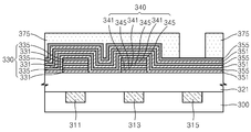
도 6은 본 발명의 실시예에 따른 무기 칼라필터를 구비한 이미지 센서의 개략적인 단면도를 도시한 것이다. 도 6을 참조하면, 이미지 센서는 반도체 기판(300)내에 형성된 다수의 포토다이오드 영역(311, 313, 315)과, 상기 다수의 포토 다이오드 영역(311, 313, 315)에 대응하여 배열되는 다수의 칼라필터(330, 340, 350) 및 상기 다수의 칼라필터(330, 340, 350)에 대응하여 배열되는 다수의 마이크로 렌즈(361, 363, 365)를 구비한다. 또한, 상기 이미지 센서는 상기 반도체 기판(300)과 칼라필터(330, 340, 350)사이에 개재된 층간 절연막(321)과, 상기 다수의 칼라필터(330, 340, 350)를 덮도록 상기 층간 절연막(321)상에 형성된 평탄화막(325)을 더 구비한다.6 shows a schematic cross-sectional view of an image sensor with an inorganic color filter according to an embodiment of the invention. Referring to FIG. 6, the image sensor includes a plurality of
상기 칼라필터(330, 340, 350)는 각각 적, 녹 및 청색 칼라필터를 포함하며, 적어도 0.8이상의 굴절율 차를 갖는 제1 및 제2무기막(331, 335), (341, 345), (351, 355)이 2 내지 5회 교대로 반복 적층된다. 상기 적색 필터(330)의 상기 제1무기막(331)은 600 내지 800Å의 두께를 갖는 실리콘 산화막을 포함하며, 상기 제2무기막(335)은 100 내지 200Å의 두께를 갖는 실리콘막을 포함한다. 상기 녹색 필터(340)의 제1무기막(341)은 700 내지 1100Å의 두께를 갖는 실리콘 산화막 또는 800 내지 1200Å의 두께를 갖는 실리콘 옥시나이트라이드를 포함하며, 상기 제2무기막(345)은 500 내지 800Å의 두께를 갖는 실리콘막 또는 600~1000Å의 두께를 갖는 실리콘 산화막을 포함한다. 상기 청색필터(350)의 제1무기막(351)은 300 내지 600Å의 두께를 갖는 실리콘막을 포함하며, 상기 제2무기막(355)은 400 내지 800Å의 두께를 갖는 실리콘 질화막을 포함한다.The color filters 330, 340, 350 include red, green, and blue color filters, respectively, and have first and second
본 발명은 적, 녹 및 청색에 대하여 제1무기막과 제2무기막의 구성물질, 두께 및 적층횟수를 최적화시켜 칼라필터를 형성하여 줌으로써, 각각의 색에 대한 최적의 발광효율을 얻는 것이 가능하다. 본 발명의 실시예에서는 이미지 센서가 적, 녹 및 청색의 칼라필터(330, 340, 350)를 구비하는 것을 예시하였으나, 이에 반드시 한정되는 것이 아니라 굴절율 차이가 0.8이상 되는 서로 다른 무기막으로 구성된 청록색 필터, 노랑색 필터 및 자홍색 필터를 구비할 수도 있다. 또한, 상기 이미지 센서는 상기 적, 녹 및 청색 필터중 적어도 하나만을 구비할 수도 있다.According to the present invention, a color filter is formed by optimizing the constituent materials, thicknesses, and stacking times of the first inorganic film and the second inorganic film against red, green, and blue colors, thereby obtaining an optimal luminous efficiency for each color. . In the exemplary embodiment of the present invention, the image sensor includes red, green, and
도 7a 내지 도 7g는 본 발명의 실시예에 따른 무기 칼라필터를 구비하는 이미지 센서의 제조방법을 설명하기 위한 단면도이다. 도 7a를 참조하면, 반도체 기판(300)으로 상기 반도체 기판(300)과는 반대 도전형을 갖는 불순물을 이온주입하여 다수의 불순물 영역(311, 313, 315)를 형성한다. 상기 불순물 영역(311, 313, 315)은 이미지 센서의 포토다이오드 영역(311, 313, 315)이 된다. 상기 포토다이오 드 영역(311, 313, 315)을 구비한 상기 반도체 기판(300)상에 층간 절연막(321)을 형성한다. 7A to 7G are cross-sectional views illustrating a method of manufacturing an image sensor including an inorganic color filter according to an exemplary embodiment of the present invention. Referring to FIG. 7A, a plurality of
도 7b 및 도 7c를 참조하면, 상기 층간 절연막(321)상에 실리콘 산화막(331)과 실리콘막(335)을 교대로 3회 반복 증착한다. 상기 실리콘 산화막(331)은 600 내지 800Å의 두께로 형성되고, 상기 실리콘막(335)은 100 내지 200Å의 두께로 형성한다. 상기 제1포토 다이오드영역(311)에 대응하는 실리콘막(335)이 노출되도록 감광막(371)을 상기 실리콘막(335)상에 형성한다. 상기 감광막(371)을 이용하여 상기 실리콘막(335) 및 실리콘 산화막(331)을 식각하여 적색 필터(330)를 형성한다.7B and 7C, the
도 7d, 도 7e 및 도 7f를 참조하면, 상기 적색 필터(330)가 형성된 상기 층간 절연막(321)상에 실리콘 옥시나이트라이드막(341)과 실리콘막(345)을 교대로 3회 반복 증착한다. 상기 실리콘 산화막(341)은 700 내지 1100Å의 두께로 형성되고, 상기 실리콘막(345)은 500 내지 800Å의 두께로 형성한다. 상기 제2포토 다이오드영역(313)에 대응하는 실리콘막(345)이 노출되도록 감광막(373)을 상기 실리콘막(345)상에 형성한다. 상기 감광막(373)을 이용하여 상기 실리콘막(345) 및 실리콘 산화막(341)을 식각하여 녹색 필터(340)를 형성한다. 상기 녹색필터(340)는 800 내지 1200Å의 두께를 갖는 실리콘 옥시나이트라이드와 600 내지 1000Å의 두께를 갖는 실리콘 산화막의 적층구조를 가질 수도 있다.7D, 7E, and 7F, the
도 7g 및 도 7h를 참조하면, 상기 적색 필터(330) 및 녹색 필터(340)가 형성된 상기 층간 절연막(321)상에 실리콘막(351)과 실리콘 질화막(355)을 교대로 3회 반복 증착한다. 상기 실리콘막(351)은 300 내지 600Å의 두께로 형성되고, 상기 실 리콘 질화막(355)은 400 내지 800Å의 두께로 형성한다. 상기 제3포토 다이오드영역(315)에 대응하는 실리콘 질화막(355)이 노출되도록 감광막(375)을 상기 실리콘막(355)상에 형성한다. 상기 감광막(375)을 이용하여 상기 실리콘막(355) 및 실리콘 산화막(351)을 식각하여 청색 필터(350)를 형성한다.Referring to FIGS. 7G and 7H, the
이어서, 상기 층간 절연막(321)상에 상기 적, 녹 및 청색 필터(330, 340, 350)를 덮도록 평탄화막(325)을 형성한다. 상기 평탄화막(325)상에 상기 적, 녹 및 청색 필터(330, 340, 350)에 대응하여 다수의 마이크로 렌즈(361, 363, 365)를 형성한다. 이로써, 도 6의 이미지 센서가 제조된다. 다른 예로서, 상기 칼라필터 형성공정을 통해 상기 적, 녹 및 청색 필터(330, 340, 350)를 상기 포토 다이오드영역(311, 313, 315)에 대응하는 상기 반도체 기판(300)상에 바로 형성하고, 평탄화막없이 층간 절연막(325)상에 마이크로 렌즈(361, 363, 365)를 형성할 수도 있다.Next, the
도 8은 본 발명의 실시예에 따른 무기 칼라필터를 구비한 CMOS 이미지 센서의 개략적인 단면도를 도시한 것이다. 도 8을 참조하면, 반도체 기판(400)내에 다수의 포토 다이오드영역을 위한 제1불순물 영역(411, 413, 415)과 소오스영역(또는 드레인영역)을 위한 제2불순물 영역(412, 414, 416)이 이격되어 형성된다. 상기 반도체 기판(400)상에 게이트 절연막(420)이 형성되고, 상기 게이트 절연막(420)상에 게이트 전극(421, 423, 425)과 적, 녹 및 청색 필터(430, 440, 450)가 형성된다. 8 is a schematic cross-sectional view of a CMOS image sensor having an inorganic color filter according to an embodiment of the present invention. Referring to FIG. 8, a
상기 적, 녹 및 청색 칼라필터(430, 440, 450)는 교대로 3회 반복 적층되고, 굴절율 차이가 0.8이상인 제1무기막(431, 441, 451)과 제2무기막(435, 445, 455)을 구비한다. 상기 적색 필터(430)의 제1무기막(431)으로 실리콘 산화막을 600 내지 800Å의 두께로 형성되고, 상기 제2무기막(435)으로 실리콘막을 100 내지 200Å의 두께로 형성한다. 상기 녹색 필터(440)의 제1무기막(441)과 제2무기막(445)으로 실리콘 산화막과 실리콘막을 700 내지 1100Å, 500 내지 800Å의 두께로 각각 형성하거나 또는 실리콘 옥시나이트라이드막과 실리콘 산화막을 800 내지 1200Å, 600 내지 1000Å의 두께로 각각 형성한다. 상기 청색필터(450)의 제1무기막(451)과 제2무기막(455)으로 실리콘막과 실리콘 질화막을 각각 300 내지 600Å, 400 내지 800Å의 두께로 형성한다. The red, green, and
상기 적, 녹 및 청색 필터(430, 440, 450)와 게이트전극(421, 423, 425)을 덮도록 상기 게이트 절연막(420)상에 층간 절연막(461)이 형성된다. 상기 제1불순물 영역(411, 413, 415)에 대응하지 않는 상기 제1층간 절연막(461)상에 제1금속배선(471)이 형성된다. 상기 제1금속배선(471) 및 제1층간 절연막(463)상에 제2층간 절연막(473)이 형성되고, 상기 제1불순물 영역(411, 413, 415)에 대응하지 않는 상기 제2층간 절연막(463)상에 제2금속배선(473)이 형성된다. 상기 제2금속배선(473)과 상기 제2층간 절연막(463)상에 제3층간 절연막(465)이 형성된다. 상기 제1불순물 영역(411, 413, 415)에 대응하지 않는 제3층간 절연막(465)상에 제3금속배선(475)이 형성되고, 상기 제3금속배선(475)과 상기 제3층간 절연막(465)상에 제4층간 절연막(467)이 형성된다. 상기 제4층간 절연막(467)상에 상기 제1불순물 영역(411, 413, 415)에 대응하여 마이크로 렌즈(481, 483, 485)가 배열된다.An interlayer insulating
CMOS 이미지 센서의 단면구조는 도 8에 한정되지 않고 다양한 구조를 가질 수 있다. 상기 적, 녹 및 청색 필터(430, 440, 450)는 상기 제1층간 절연막(461)상 에 상기 제1금속배선(471)과 함께 형성하거나, 상기 제2층간 절연막(463)상에 상기 제2금속배선(473)과 함께 형성하거나, 또는 상기 제3층간 절연막(463)상에 상기 제3금속배선(475)과 함께 형성할 수도 있다. 또한, 상기 제4층간 절연막(467)상에 형성되고, 상기 제4층간 절연막(467)과 마이크로 렌즈(471, 473, 475)사이에 평탄화막이 개재될 수도 있다.The cross-sectional structure of the CMOS image sensor is not limited to FIG. 8 and may have various structures. The red, green, and
이상에서 자세히 설명한 바와 같이, 본 발명의 칼라필터 및 이를 구비한 CMOS 이미지 센서는 무기 칼라필터를 상기 반도체 기판상에 게이트 전극과 동일면상에 형성하여 줌으로써 통상적인 CMOS 이미지 센서에서 칼라필터와 마이크로 렌즈사이에 개재되는 보호막 및 평탄화막의 형성공정을 배제시킬 수 있으므로, 공정을 단순화시킬 수 있을 뿐만 아니라 이미지 센서의 수직 두께 감소에 따른 고집적화가 가능하다. 또한, 칼라필터를 구성하는 제1 및 제2무기막을 일정이상의 굴절율 차를 갖는 무기물질로 형성하여 제1 및 제2무기막의 적층횟수를 감소시켜 줄 수 있으므로, 소자의 고집적화가 유리하다. As described in detail above, the color filter of the present invention and the CMOS image sensor having the same are formed between the color filter and the microlens in the conventional CMOS image sensor by forming an inorganic color filter on the same surface as the gate electrode on the semiconductor substrate. Since the process of forming the protective film and the planarization film interposed therebetween can be eliminated, not only the process can be simplified, but also high integration can be achieved by reducing the vertical thickness of the image sensor. In addition, since the first and second inorganic films constituting the color filter may be formed of an inorganic material having a difference in refractive index of a predetermined value or more, the number of stacking of the first and second inorganic films may be reduced, so that the device is highly integrated.
이상 본 발명을 바람직한 실시예를 들어 상세하게 설명하였으나, 본 발명은 상기 실시예에 한정되지 않고, 본 발명의 기술적 사상의 범위 내에서 당 분야에서 통상의 지식을 가진 자에 의하여 여러가지 변형이 가능하다.Although the present invention has been described in detail with reference to preferred embodiments, the present invention is not limited to the above embodiments, and various modifications may be made by those skilled in the art within the scope of the technical idea of the present invention. .
Claims (31)
Priority Applications (5)
| Application Number | Priority Date | Filing Date | Title |
|---|---|---|---|
| KR1020060013710A KR100790981B1 (en) | 2006-02-13 | 2006-02-13 | Color filter, color filter array and fabrication method thereof and image sensor |
| US11/668,120 US7875947B2 (en) | 2006-02-13 | 2007-01-29 | Filter, color filter array, method of manufacturing the color filter array, and image sensor |
| DE102007006921A DE102007006921B4 (en) | 2006-02-13 | 2007-02-06 | Color filter, color filter field, manufacturing method and image sensor |
| JP2007030810A JP5247042B2 (en) | 2006-02-13 | 2007-02-09 | Color filter array and image sensor |
| TW096104756A TWI361487B (en) | 2006-02-13 | 2007-02-09 | Filter, color filter array, method of manufacturing the color filter array, and image sensor |
Applications Claiming Priority (1)
| Application Number | Priority Date | Filing Date | Title |
|---|---|---|---|
| KR1020060013710A KR100790981B1 (en) | 2006-02-13 | 2006-02-13 | Color filter, color filter array and fabrication method thereof and image sensor |
Publications (2)
| Publication Number | Publication Date |
|---|---|
| KR20070081627A KR20070081627A (en) | 2007-08-17 |
| KR100790981B1 true KR100790981B1 (en) | 2008-01-02 |
Family
ID=38367519
Family Applications (1)
| Application Number | Title | Priority Date | Filing Date |
|---|---|---|---|
| KR1020060013710A KR100790981B1 (en) | 2006-02-13 | 2006-02-13 | Color filter, color filter array and fabrication method thereof and image sensor |
Country Status (5)
| Country | Link |
|---|---|
| US (1) | US7875947B2 (en) |
| JP (1) | JP5247042B2 (en) |
| KR (1) | KR100790981B1 (en) |
| DE (1) | DE102007006921B4 (en) |
| TW (1) | TWI361487B (en) |
Cited By (1)
| Publication number | Priority date | Publication date | Assignee | Title |
|---|---|---|---|---|
| KR101220143B1 (en) | 2011-06-27 | 2013-01-11 | 어보브반도체 주식회사 | One-chip semiconductor apparatus for photo detectors with different receiving band and integrated circuit and manufacturing method thereof |
Families Citing this family (28)
| Publication number | Priority date | Publication date | Assignee | Title |
|---|---|---|---|---|
| KR101176545B1 (en) * | 2006-07-26 | 2012-08-28 | 삼성전자주식회사 | Method for forming micro-lens and image sensor comprising micro-lens and method for manufacturing the same |
| CN101459184B (en) * | 2007-12-13 | 2011-03-23 | 中芯国际集成电路制造(上海)有限公司 | System and method for sensing image on CMOS |
| US7924504B2 (en) * | 2008-01-01 | 2011-04-12 | United Microelectronics Corp. | Color filter structure having inorganic layers |
| US8063465B2 (en) * | 2008-02-08 | 2011-11-22 | Omnivision Technologies, Inc. | Backside illuminated imaging sensor with vertical pixel sensor |
| US7701636B2 (en) | 2008-03-06 | 2010-04-20 | Aptina Imaging Corporation | Gradient index microlenses and method of formation |
| KR101500344B1 (en) * | 2008-08-26 | 2015-03-09 | 삼성전자 주식회사 | Image Sensor |
| US7833818B2 (en) | 2008-12-14 | 2010-11-16 | United Microelectronics Corp. | Integrated structure of MEMS device and CMOS image sensor device and fabricating method thereof |
| US8264377B2 (en) | 2009-03-02 | 2012-09-11 | Griffith Gregory M | Aircraft collision avoidance system |
| JP4741015B2 (en) * | 2009-03-27 | 2011-08-03 | 富士フイルム株式会社 | Image sensor |
| JP5534927B2 (en) | 2010-05-06 | 2014-07-02 | 株式会社東芝 | Solid-state imaging device |
| US8643140B2 (en) | 2011-07-11 | 2014-02-04 | United Microelectronics Corp. | Suspended beam for use in MEMS device |
| US8525354B2 (en) | 2011-10-13 | 2013-09-03 | United Microelectronics Corporation | Bond pad structure and fabricating method thereof |
| US9568362B2 (en) | 2012-12-19 | 2017-02-14 | Viavi Solutions Inc. | Spectroscopic assembly and method |
| US9448346B2 (en) | 2012-12-19 | 2016-09-20 | Viavi Solutions Inc. | Sensor device including one or more metal-dielectric optical filters |
| US10197716B2 (en) | 2012-12-19 | 2019-02-05 | Viavi Solutions Inc. | Metal-dielectric optical filter, sensor device, and fabrication method |
| KR102149937B1 (en) * | 2013-02-22 | 2020-09-01 | 삼성전자주식회사 | Photoelectronic device and image sensor |
| US8981501B2 (en) | 2013-04-25 | 2015-03-17 | United Microelectronics Corp. | Semiconductor device and method of forming the same |
| US9746678B2 (en) * | 2014-04-11 | 2017-08-29 | Applied Materials | Light wave separation lattices and methods of forming light wave separation lattices |
| US9293488B2 (en) * | 2014-05-07 | 2016-03-22 | Visera Technologies Company Limited | Image sensing device |
| KR102413524B1 (en) * | 2014-06-18 | 2022-06-24 | 비아비 솔루션즈 아이엔씨. | Metal-dielectric optical filter, sensor device, and fabrication method |
| CN104157790B (en) * | 2014-06-30 | 2017-03-15 | 上海天马有机发光显示技术有限公司 | A kind of organic light emitting film encapsulating structure, its device, device and manufacture method |
| KR102240020B1 (en) | 2014-08-29 | 2021-04-14 | 삼성전자주식회사 | Electronic device having a color filter |
| KR102648400B1 (en) * | 2016-02-22 | 2024-03-18 | 삼성디스플레이 주식회사 | Quantum dot color filter and display device including the same |
| EP3258493B1 (en) | 2016-06-16 | 2021-01-27 | ams AG | System-on-chip camera with integrated light sensor(s) and method of producing a system-on-chip camera |
| JP7062692B2 (en) | 2018-02-20 | 2022-05-06 | インテリジェント クリーニング イクイップメント ホールディングス カンパニー リミテッド | Tracking system, object tracking system, and related usage |
| CN109148500A (en) * | 2018-08-28 | 2019-01-04 | 德淮半导体有限公司 | Double-layer color optical filter and forming method thereof |
| CN109891278B (en) * | 2019-01-23 | 2021-10-15 | 京东方科技集团股份有限公司 | Light filtering structure, light filtering layer and display panel |
| US11682313B2 (en) | 2021-03-17 | 2023-06-20 | Gregory M. Griffith | Sensor assembly for use in association with aircraft collision avoidance system and method of using the same |
Citations (4)
| Publication number | Priority date | Publication date | Assignee | Title |
|---|---|---|---|---|
| KR20020027016A (en) * | 2000-10-04 | 2002-04-13 | 박종섭 | Image sensor capable of preventing generation of scum and overlap between color filters and method for forming the same |
| KR20030057611A (en) * | 2001-12-29 | 2003-07-07 | 주식회사 하이닉스반도체 | Image sensor with improved blue signal sensitivity |
| KR20060005575A (en) * | 2004-07-13 | 2006-01-18 | 동부아남반도체 주식회사 | Cmos image sensor and method for fabricating of the same |
| KR20060010884A (en) * | 2004-07-29 | 2006-02-03 | 매그나칩 반도체 유한회사 | Image sensor having notch filter and method for fabrication of the same |
Family Cites Families (16)
| Publication number | Priority date | Publication date | Assignee | Title |
|---|---|---|---|---|
| JPS5527778A (en) * | 1978-08-18 | 1980-02-28 | Semiconductor Res Found | Semiconductor color pickup device |
| JPS62119502A (en) | 1985-11-18 | 1987-05-30 | インタ−ナショナル ビジネス マシ−ンズ コ−ポレ−ション | Spectrum-filter |
| JPS6348234A (en) * | 1986-08-14 | 1988-02-29 | Fuji Sekiyu Kk | Production of 2,5-di(chloromethyl)-p-xylene |
| JPS63172461A (en) | 1987-01-12 | 1988-07-16 | Seiko Epson Corp | Color image sensor |
| US5246803A (en) * | 1990-07-23 | 1993-09-21 | Eastman Kodak Company | Patterned dichroic filters for solid state electronic image sensors |
| KR920015461A (en) * | 1991-01-10 | 1992-08-26 | 김광호 | Color filter and its manufacturing method |
| US5711889A (en) * | 1995-09-15 | 1998-01-27 | Buchsbaum; Philip E. | Method for making dichroic filter array |
| JPH1090677A (en) * | 1996-09-04 | 1998-04-10 | Internatl Business Mach Corp <Ibm> | Reflection type display device and its color development method |
| JPH10163462A (en) * | 1996-11-29 | 1998-06-19 | Sony Corp | Solid-state image sensing device of mass type filter structure and its manufacture |
| KR100297984B1 (en) | 1999-03-24 | 2001-09-26 | 구본준, 론 위라하디락사 | A color filter plate and a fabricating method thereof |
| KR100776145B1 (en) | 2001-06-30 | 2007-11-15 | 매그나칩 반도체 유한회사 | Image sensor with multilayer color filter |
| JP4269730B2 (en) * | 2003-03-18 | 2009-05-27 | ソニー株式会社 | Solid-state imaging device and manufacturing method thereof |
| WO2005013369A1 (en) * | 2003-08-01 | 2005-02-10 | Matsushita Electric Industrial Co., Ltd. | Solid-state imaging device, production method for solid-state imaging device and camera using this |
| US7759679B2 (en) | 2004-01-15 | 2010-07-20 | Panasonic Corporation | Solid-state imaging device, manufacturing method of solid-state imaging device, and camera employing same |
| KR100753391B1 (en) * | 2004-05-14 | 2007-08-30 | 매그나칩 반도체 유한회사 | cmos image sensor |
| JP2006032967A (en) * | 2004-07-16 | 2006-02-02 | Samsung Electronics Co Ltd | Image sensor and manufacturing method of same |
-
2006
- 2006-02-13 KR KR1020060013710A patent/KR100790981B1/en not_active IP Right Cessation
-
2007
- 2007-01-29 US US11/668,120 patent/US7875947B2/en not_active Expired - Fee Related
- 2007-02-06 DE DE102007006921A patent/DE102007006921B4/en not_active Expired - Fee Related
- 2007-02-09 TW TW096104756A patent/TWI361487B/en not_active IP Right Cessation
- 2007-02-09 JP JP2007030810A patent/JP5247042B2/en not_active Expired - Fee Related
Patent Citations (4)
| Publication number | Priority date | Publication date | Assignee | Title |
|---|---|---|---|---|
| KR20020027016A (en) * | 2000-10-04 | 2002-04-13 | 박종섭 | Image sensor capable of preventing generation of scum and overlap between color filters and method for forming the same |
| KR20030057611A (en) * | 2001-12-29 | 2003-07-07 | 주식회사 하이닉스반도체 | Image sensor with improved blue signal sensitivity |
| KR20060005575A (en) * | 2004-07-13 | 2006-01-18 | 동부아남반도체 주식회사 | Cmos image sensor and method for fabricating of the same |
| KR20060010884A (en) * | 2004-07-29 | 2006-02-03 | 매그나칩 반도체 유한회사 | Image sensor having notch filter and method for fabrication of the same |
Cited By (1)
| Publication number | Priority date | Publication date | Assignee | Title |
|---|---|---|---|---|
| KR101220143B1 (en) | 2011-06-27 | 2013-01-11 | 어보브반도체 주식회사 | One-chip semiconductor apparatus for photo detectors with different receiving band and integrated circuit and manufacturing method thereof |
Also Published As
| Publication number | Publication date |
|---|---|
| US20070187793A1 (en) | 2007-08-16 |
| DE102007006921A1 (en) | 2007-09-20 |
| DE102007006921B4 (en) | 2009-06-10 |
| TW200737508A (en) | 2007-10-01 |
| TWI361487B (en) | 2012-04-01 |
| JP2007219515A (en) | 2007-08-30 |
| JP5247042B2 (en) | 2013-07-24 |
| KR20070081627A (en) | 2007-08-17 |
| US7875947B2 (en) | 2011-01-25 |
Similar Documents
| Publication | Publication Date | Title |
|---|---|---|
| KR100790981B1 (en) | Color filter, color filter array and fabrication method thereof and image sensor | |
| US20080159658A1 (en) | Image Sensor and Method for Manufacturing The Same | |
| JP4623641B2 (en) | Method for manufacturing solid-state imaging device | |
| CN101414614B (en) | Image sensor device and fabrication method thereof | |
| TWI600147B (en) | Method of fabricating an image sensor | |
| JP2006210701A (en) | Solid-state image sensing device and its manufacturing method | |
| KR100832710B1 (en) | Image sensor and method of manufacturing the same | |
| US7611922B2 (en) | Image sensor and method for manufacturing the same | |
| CN101677082A (en) | CMOS image sensor and method for fabricating the same | |
| KR20050106939A (en) | Cmos image sensor having prism and fabricating method thereof | |
| JP2009080313A (en) | Color filter and its manufacturing method, solid-state imaging element using this filter and its manufacturing method | |
| JP2006351775A (en) | Method of manufacturing color filter, method of manufacturing solid-state imaging device and the solid-state imaging device employing the filter | |
| US20070102716A1 (en) | Image sensor and fabricating method thereof | |
| JP2007147738A (en) | Color filter and its manufacturing method, and solid-state imaging element using the same and its manufacturing method | |
| KR20080053569A (en) | Pattern mask used for forming micro lense, image sensor and method of manufacturing the same | |
| JP4435606B2 (en) | Solid-state imaging device and camera | |
| US20080157246A1 (en) | Image sensor and fabricating method thereof | |
| KR100449951B1 (en) | Image sensor and method of fabricating the same | |
| KR20010061343A (en) | Method for fabricating image sensor | |
| KR20040058664A (en) | CMOS image sensor and fabricating method of the same | |
| KR20010061078A (en) | Method for fabricating image sensor with correct color image | |
| CN101419975A (en) | Image sensor and method for manufacturing thereof | |
| KR100967744B1 (en) | Cmos image sensor with bi-convex microlense and fabricating method of the same | |
| KR20010061341A (en) | Method for fabricating image sensor | |
| KR100776145B1 (en) | Image sensor with multilayer color filter |
Legal Events
| Date | Code | Title | Description |
|---|---|---|---|
| A201 | Request for examination | ||
| E902 | Notification of reason for refusal | ||
| E701 | Decision to grant or registration of patent right | ||
| GRNT | Written decision to grant | ||
| FPAY | Annual fee payment |
Payment date: 20121130 Year of fee payment: 6 |
|
| FPAY | Annual fee payment |
Payment date: 20131129 Year of fee payment: 7 |
|
| LAPS | Lapse due to unpaid annual fee |