KR100788426B1 - Back light unit and liquid crystal display comprising the same - Google Patents
Back light unit and liquid crystal display comprising the same Download PDFInfo
- Publication number
- KR100788426B1 KR100788426B1 KR1020050111041A KR20050111041A KR100788426B1 KR 100788426 B1 KR100788426 B1 KR 100788426B1 KR 1020050111041 A KR1020050111041 A KR 1020050111041A KR 20050111041 A KR20050111041 A KR 20050111041A KR 100788426 B1 KR100788426 B1 KR 100788426B1
- Authority
- KR
- South Korea
- Prior art keywords
- diffusion lens
- point
- curved portion
- liquid crystal
- curve
- Prior art date
Links
Images


Classifications
-
- G—PHYSICS
- G02—OPTICS
- G02F—OPTICAL DEVICES OR ARRANGEMENTS FOR THE CONTROL OF LIGHT BY MODIFICATION OF THE OPTICAL PROPERTIES OF THE MEDIA OF THE ELEMENTS INVOLVED THEREIN; NON-LINEAR OPTICS; FREQUENCY-CHANGING OF LIGHT; OPTICAL LOGIC ELEMENTS; OPTICAL ANALOGUE/DIGITAL CONVERTERS
- G02F1/00—Devices or arrangements for the control of the intensity, colour, phase, polarisation or direction of light arriving from an independent light source, e.g. switching, gating or modulating; Non-linear optics
- G02F1/01—Devices or arrangements for the control of the intensity, colour, phase, polarisation or direction of light arriving from an independent light source, e.g. switching, gating or modulating; Non-linear optics for the control of the intensity, phase, polarisation or colour
- G02F1/13—Devices or arrangements for the control of the intensity, colour, phase, polarisation or direction of light arriving from an independent light source, e.g. switching, gating or modulating; Non-linear optics for the control of the intensity, phase, polarisation or colour based on liquid crystals, e.g. single liquid crystal display cells
- G02F1/133—Constructional arrangements; Operation of liquid crystal cells; Circuit arrangements
- G02F1/1333—Constructional arrangements; Manufacturing methods
- G02F1/1335—Structural association of cells with optical devices, e.g. polarisers or reflectors
- G02F1/1336—Illuminating devices
- G02F1/133602—Direct backlight
- G02F1/133603—Direct backlight with LEDs
-
- H—ELECTRICITY
- H01—ELECTRIC ELEMENTS
- H01L—SEMICONDUCTOR DEVICES NOT COVERED BY CLASS H10
- H01L33/00—Semiconductor devices with at least one potential-jump barrier or surface barrier specially adapted for light emission; Processes or apparatus specially adapted for the manufacture or treatment thereof or of parts thereof; Details thereof
- H01L33/48—Semiconductor devices with at least one potential-jump barrier or surface barrier specially adapted for light emission; Processes or apparatus specially adapted for the manufacture or treatment thereof or of parts thereof; Details thereof characterised by the semiconductor body packages
- H01L33/58—Optical field-shaping elements
Abstract
본 발명은 백라이트 유닛 및 이를 포함하는 액정표시장치에 관한 것이다. 본 발명에 따른 백라이트 유닛은, 점광원 회로기판과; 상기 점광원 회로기판 상에 장착되어 있는 복수의 점광원과; 상기 각 점광원 상에 마련되며, 함몰점과 상기 함몰점으로부터 방사상으로 돌출되어 있는 곡면부를 갖는 확산렌즈를 포함한다. 이에 의해 색 균일성이 향상되고, 광효율이 증가하는 백라이트 유닛 및 이를 포함하는 액정표시장치가 제공된다. The present invention relates to a backlight unit and a liquid crystal display including the same. A backlight unit according to the present invention includes a point light source circuit board; A plurality of point light sources mounted on said point light source circuit board; And a diffusion lens provided on each point light source and having a curved portion and a curved portion projecting radially from the recessed point. As a result, a backlight unit having improved color uniformity and increased light efficiency and a liquid crystal display including the same are provided.
Description
도 1은 본 발명의 제1실시예에 따른 액정표시장치의 분해사시도이고,1 is an exploded perspective view of a liquid crystal display according to a first embodiment of the present invention;
도 2는 본 발명의 제1실시예에 따른 확산렌즈의 단면도 및 사시도이고,2 is a cross-sectional view and a perspective view of a diffusion lens according to a first embodiment of the present invention;
도 3은 본 발명의 제2실시예에 따른 확산렌즈의 단면도이고,3 is a cross-sectional view of a diffusion lens according to a second embodiment of the present invention;
도 4는 본 발명의 제3실시예에 따른 확산렌즈의 단면도이고,4 is a cross-sectional view of a diffusion lens according to a third embodiment of the present invention;
도 5는 본 발명의 제1실시예에 따른 확산렌즈 및 종래의 확산렌즈의 휘도를 도시한 그래프이다. 5 is a graph showing the luminance of the diffusion lens and the conventional diffusion lens according to the first embodiment of the present invention.
* 도면의 주요 부분에 대한 부호의 설명 *Explanation of symbols on the main parts of the drawings
10 : 탑 샤시 20 : 액정표시패널10: top chassis 20: liquid crystal display panel
30 : 광조절부재 40 : 반사판30: light adjusting member 40: reflecting plate
51 : 회로기판 60 : 발광 다이오드51: circuit board 60: light emitting diode
70, 80, 90 : 확산렌즈 100 : 하부 샤시70, 80, 90: Diffusion lens 100: Lower chassis
본 발명은 백라이트 유닛 및 이를 포함하는 액정표시장치관한 것으로서, 보 다 상세하게는, 점광원을 포함하는 백라이트 유닛 및 이를 포함하는 액정표시장치에 관한 것이다. The present invention relates to a backlight unit and a liquid crystal display including the same, and more particularly, to a backlight unit including a point light source and a liquid crystal display including the same.
최근 종래의 CRT를 대신하여 액정표시장치(LCD), PDP(plasma display panel), OLED(organic light emitting diode) 등의 평판표시장치가 많이 개발되고 있다. Recently, a flat panel display such as a liquid crystal display (LCD), a plasma display panel (PDP), or an organic light emitting diode (OLED) has been developed in place of the conventional CRT.
이 중 액정표시장치는 박막트랜지스터 기판, 컬러필터 기판 그리고 양 기판 사이에 액정이 주입되어 있는 액정표시패널을 포함한다. 액정표시패널은 비발광소자이기 때문에 박막트랜지스터 기판의 후면에는 빛을 공급하기 위한 백라이트 유닛이 위치한다. 백라이트 유닛에서 조사된 빛은 액정의 배열 상태에 따라 투과량이 조정된다. 액정표시패널과 백라이트 유닛은 샤시 내에 수용되어 있다.The liquid crystal display device includes a thin film transistor substrate, a color filter substrate, and a liquid crystal display panel in which liquid crystal is injected between both substrates. Since the liquid crystal display panel is a non-light emitting device, a backlight unit for supplying light is disposed on the rear surface of the thin film transistor substrate. Light transmitted from the backlight unit is adjusted according to the arrangement of the liquid crystals. The liquid crystal display panel and the backlight unit are housed in the chassis.
백라이트 유닛은 광원의 위치에 따라 에지형과 직하형으로 구분된다. 에지형은 도광판의 측면에 광원이 설치되는 구조로 주로, 랩탑형 및 데스크탑 컴퓨터와 같이 비교적 크기가 작은 액정표시장치에 적용된다. 이러한 에지형 백라이트 유닛은 빛의 균일성이 좋고, 내구 수명이 길며, 액정표시장치의 박형화에 유리하다. 하지만, 발광된 빛이 도광판을 통과하는 과정에서 유실되기 때문에 광효율이 감소되는 문제점이 있고, 대형 액정표시패널의 경우 도광판을 하나의 금형으로 제조할 수 없는 제약이 존재한다.The backlight unit is divided into an edge type and a direct type according to the position of the light source. The edge type is a structure in which a light source is installed on the side of the light guide plate, and is mainly applied to a relatively small liquid crystal display device such as a laptop type and a desktop computer. Such an edge type backlight unit has a good light uniformity, a long service life, and is advantageous for thinning a liquid crystal display device. However, there is a problem that the light efficiency is reduced because the emitted light is lost in the process of passing through the light guide plate, and in the case of a large liquid crystal display panel, there is a limitation in that the light guide plate cannot be manufactured in one mold.
직하형은 액정표시장치의 크기가 대형화 되면서 중점적으로 개발된 구조로, 액정표시패널의 하부면에 하나 이상의 광원을 배치시켜 액정표시패널에 전면적으로 빛을 공급하는 구조이다. 이러한 직하형 백라이트 유닛은 에지형 백라이트 유닛에 비해 많은 수의 광원을 이용할 수 있어 높은 휘도를 확보할 수 있는 장점이 있는 반면, 색얼룩이 발생하여 휘도가 균일하지 않은 단점이 있다. The direct type is a structure that is mainly developed as the size of the liquid crystal display device increases in size, and it is a structure in which one or more light sources are disposed on the lower surface of the liquid crystal display panel to supply light to the liquid crystal display panel in full. Such a direct type backlight unit has a merit that a large number of light sources can be used as compared to an edge type backlight unit, thereby ensuring a high luminance, while color spots are generated, resulting in a non-uniform luminance.
따라서, 본 발명의 목적은 색 균일성이 향상되고, 광효율이 증가하는 백라이트 유닛 및 이를 포함하는 액정표시장치가 제공하는 것이다.Accordingly, an object of the present invention is to provide a backlight unit and a liquid crystal display including the same, which improve color uniformity and increase light efficiency.
상기 목적은, 본 발명에 따라 백라이트 유닛에 있어서, 점광원 회로기판과; 상기 점광원 회로기판 상에 장착되어 있는 복수의 점광원과; 상기 각 점광원 상에 마련되며, 함몰점과 상기 함몰점으로부터 방사상으로 돌출되어 있는 곡면부를 갖는 확산렌즈를 포함하는 백라이트 유닛에 의해 달성된다.The object of the present invention is to provide a backlight unit comprising: a point light source circuit board; A plurality of point light sources mounted on said point light source circuit board; It is achieved by a backlight unit provided on each of the point light sources and including a diffusion lens having a depression point and a curved portion projecting radially from the depression point.
상기 곡면부의 단면은 정상부를 갖는 비원형 곡선을 포함하며, 상기 비원형 곡선은 상기 함몰점를 포함하는 축에 대하여 대칭일 수 있다. 비원형 곡선은 둘 이상의 원형 곡선 또는 상이한 직선을 포함할 수도 있다.The cross section of the curved portion includes a non-circular curve having a top portion, and the non-circular curve may be symmetric about an axis including the depression point. Non-circular curves may include two or more circular curves or different straight lines.
상기 함몰점은 상기 점광원과 소정의 간격으로 이격되어 있는 것이 바람직하다. The depression point is preferably spaced apart from the point light source at a predetermined interval.
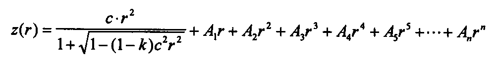
상기 곡면부는 다음 식에 의하여 형성되며, 여기서 A1≠0일 수 있다. A1≠0인 것을 함몰점의 형성을 의미하는 것으로 함몰 부위에 의해 빛을 칩의 상부가 아닌 주변부로 효율적으로 확산시키는 효과가 있다. The curved portion is formed by the following equation, where A1 ≠ 0. A1 ≠ 0 means the formation of a depression point, which has the effect of efficiently diffusing light to the periphery rather than the top of the chip by the depression.

( C : 확산렌즈의 곡률, k : 코닉상수, r=(x2+y2)1/2 : xyz 죄표 상에서 원점으로부터 xy 평면 상의 임의의 점(x y)까지의 거리, A : 비구면 계수)(C: curvature of the diffuse lens, k: conic constant, r = (x 2 + y 2 ) 1/2 : distance from the origin on the xyz plot to an arbitrary point (xy) on the xy plane, A: aspherical coefficient)
상기 확산렌즈는 상기 점광원에 인접한 제1렌즈면 및 상기 함몰점을 포함하는 곡면의 제2렌즈면을 포함하며, 상기 C 가 음수이고, 상기 A1은 양수인 것이 바람직하다.The diffusion lens includes a first lens surface adjacent to the point light source and a curved second lens surface including the depression, wherein C is negative and A 1 is positive.
상기 곡면부의 단면은 원형 곡선을 포함하며, 상기 원형 곡선은 상기 함몰점를 포함하는 축에 대하여 대칭일 수 있다.The cross section of the curved portion may include a circular curve, and the circular curve may be symmetric about an axis including the depression point.
상기 곡면부 단면은 적어도 상이한 둘 이상의 원형 곡선이 중첩되어 형성된 곡선을 포함하며, 상기 곡선은 상기 함몰점를 포함하는 축에 대하여 대칭일 수 있다.The curved section cross-section includes a curve formed by overlapping at least two different circular curves, and the curve may be symmetric about an axis including the depression point.
상기 확산렌즈의 표면에 형성되어 있는 요철부를 더 포함하여 빛의 산란을 유도하고, 이로 인하여 휘도 분포 균일도 및 색균일도를 증가시키는 것이 바람직하다. It is preferable to further include scattering portions formed on the surface of the diffusion lens to induce scattering of light, thereby increasing luminance distribution uniformity and color uniformity.
한편, 상기 목적은, 본 발명에 따라 액정패널과; 상기 액정패널 배면 전체에 마련되어 있는 점광원과; 상기 액정패널 및 상기 각 점광원의 사이에 마련되며, 함몰점과 상기 함몰점으로부터 방사상으로 돌출되어 있는 곡면부를 갖는 확산렌즈를 포함하는 액정표시장치에 의해서도 달성될 수 있다.On the other hand, the above object, the liquid crystal panel according to the present invention; A point light source provided on the entire rear surface of the liquid crystal panel; It can also be achieved by a liquid crystal display device provided between the liquid crystal panel and the point light source, and including a diffusion lens having a depression point and a curved portion projecting radially from the depression point.
이하에서는 첨부도면을 참조하여 본 발명에 대하여 설명한다.Hereinafter, the present invention will be described with reference to the accompanying drawings.
여러 실시예에 있어서 동일한 구성요소에 대하여서는 동일한 참조번호를 부여 하였으며, 동일한 구성요소에 대하여는 제1실시예에서 대표적으로 설명하고 다른 실시예에서는 생략될 수 있다.In various embodiments, like reference numerals refer to like elements, and like reference numerals refer to like elements in the first embodiment and may be omitted in other embodiments.
본 발명의 제1실시예에 따른 액정표시장치는 도1, 도2 및 도5를 참조하여 설명된다. 도1은 본 발명의 제1실시예에 따른 액정표시장치의 분해 사시도, 도2는 본 발명의 제1실시예에 따른 액정표시장치의 단면도, 도5는 본 실시예에 따른 확산렌즈와 종래의 확산렌즈의 휘도를 도시한 그래프이다.The liquid crystal display device according to the first embodiment of the present invention will be described with reference to FIGS. 1, 2 and 5. 1 is an exploded perspective view of a liquid crystal display device according to a first embodiment of the present invention, FIG. 2 is a cross-sectional view of a liquid crystal display device according to a first embodiment of the present invention, and FIG. 5 is a diffusion lens according to the present embodiment. It is a graph showing the luminance of the diffusion lens.
액정표시장치(1)는 액정표시패널(20), 액정표시패널(20)의 배면에 순차적으로 위치한 광조절부재(30), 반사판(40), 발광 다이오드 회로기판(51) 그리고, 발광 다이오드 회로기판(51)에 실장되어 있으며 반사판(40)의 수용구(41)에 위치하고 있는 발광 다이오드(60)를 포함한다.The liquid crystal display device 1 includes a liquid
액정표시패널(20), 광조절부재(30), 발광 다이오드 회로기판(51)은 상부 샤시(10)와 하부 샤시(100)에 수용되어 있다.The liquid
액정표시패널(20)은 박막트랜지스터가 형성되어 있는 박막트랜지스 기판(21)과 박막트랜지스 기판(21)과 대면하고 있는 컬러필터 기판(22), 양 기판(21, 22)을 접합시키며 셀갭(cell gap)을 형성하는 실런트(23), 양 기판(21, 22)과 실런트(23) 사이에 위치하는 액정층(24)을 포함한다. 제1실시예에서 액정표시패널(20)은 장변과 단변을 가지는 직사각형 형태로 마련되어 있다. The liquid
액정표시패널(20)은 액정층(24)의 배열을 조정하여 화면을 형성하지만 비발광소자이기 때문에 배면에 위치한 발광 다이오드(60)로부터 빛을 공급받아야 한다. 박막트랜지스터 기판(21)의 일 측에는 구동신호 인가를 위한 구동부(25)가 마련되어 있다. 구동부(24)는 연성인쇄회로기판(FPC; 26), 연성인쇄회로기판(26)에 장착되어 있는 구동칩(27), 연성인쇄회로기판(26)의 타 측에 연결되어 있는 회로기판(PCB; 28)을 포함한다. 도시된 구동부(25)는 COP(chip on film) 방식을 나타낸 것이며, TCP(tape carrier package), COG(chip on glass) 등 공지의 다른 방식도 가 능하다. 또한, 구동부(25)가 배선형성과정에서 박막트랜지스터 기판(21)에 형성되는 것도 가능하다.The liquid
액정표시패널(20)의 배면에 위치하는 광조절부재(30)는 확산판(31), 프리즘 필름(32) 및 보호필름(33)을 포함할 수 있다.The
확산판(31)은 베이스판과 베이스판에 형성된 구슬 모양의 비드를 포함하는 코팅층으로 이루어져 있다. 확산판(31)은 발광 다이오드(60)에서 공급된 빛을 확산시켜 휘도를 균일하게 한다.The
프리즘 필름(32)은 상부면에 삼각기둥 모양의 프리즘이 일정한 배열을 갖고 형성되어 있다. 프리즘 필름(32)은 확산한(31)에서 확산된 빛을 상부의 액정표시패널(20)의 배치 평면에 수직한 방향으로 집광하는 역할을 수행한다. 프리즘 필름(32)은 통산 2장이 사용되며 각 프리즘 필름(32)에 형성된 마이크로 프리즘은 소정의 각도를 이루고 있다. 프리즘 필름(32)을 통과한 빛은 거의 대부분 수직하게 진행되어 균일한 휘도 분포를 제공하게 된다. 필요에 따라 프리즘 필름(32)과 함께 반사 편광필름을 사용할 수 있으며, 프리즘 필름(32) 없이 반사편광필름만을 사용하는 것도 가능하다. The
가장 상부에 위치하는 보호필름(33)은 스크래치에 약한 프리즘 필름(32)을 보호한다. The
발광 다이오드(60)가 실장되어 있지 않은 발광 다이오드 회로기판(51) 상에는 반사판(40)이 마련되어 있다. 반사판(40)에는 발광 다이오드(60)의 배치에 대응하는 발광 다이오드 수용구(41)가 마련되어 있다. 발광 다이오드 수용구(41)는 서 로 평행한 적어도 하나 이상의 열로 이루어져 있으며, 각 열에는 하나 이상의 발광 다이오드 수용구(41)가 서로 일정한 간격으로 형성되어 있다. 발광 다이오드 수용구(41)는 인접한 열 간에는 서로 엇갈리게 배치되어 있다. 각 발광 다이오드 수용구(41)에는 발광 다이오드(60)의 백색광 공급 유닛(61)이 위치하며, 발광 다이오드 수용구(41)는 백색광 공급유닛(61)에 비해 다소 크게 형성될 수 있다.The reflecting
발광 다이오드(60)는 빛을 발생시키는 칩(62)을 비롯한 대부분이 반사판(40)보다 높게 위치한다. 반사판(40)은 하부로 입사되는 빛을 반사시켜 확산판(31)으로 공급하는 역할을 한다. 반사판(40)은 폴리에틸렌테레프탈레이트(PET)나 폴리카보네이트(PC)로 만들어 질 수 있으며 은이나 알루미늄이 코팅되어 있을 수도 있다. 또한 반사판(40)은 발광 다이오드(60)에서 발생하는 강한 열에 의해 움이 발생하지 않도록 다소 두껍게 마련될 수 있다. Most of the
발광 다이오드(60)에서 열이 많이 발생하므로 발광 다이오드 회로기판(51)은 열전달율이 우수한 알루미늄을 주재료로 사용하여 만들어질 수 있다. 도시하지는 않았지만 열 방출을 용이하게 하기 위해 액정표시장치(1)는 히트 파이프, 방열핀, 냉각팬 등을 더 포함할 수도 있다. Since a large amount of heat is generated in the
발광 다이오드(60)는 발광 다이오드 회로기판(51)에 실장되어 있으며 액정표시패널(20)의 배면 전체에 걸쳐 배치되어 있다. 발광 다이오드(60)는 백색광을 공급하는 복수의 백색광 공급유닛(61)을 포함하는데, 제1실시예에서 백색광 공급유닛(61)은 각각 하나씩의 적색 발광 다이오드, 청색 발광 다이오드와 한 쌍의 녹색 발광 다이오드로 구성되어 있다. 백색광 공급 유닛(61)은 발광 다이오드 회로기판 (51)에 일정한 간격으로 배치되어 있다.The
발광 다이오드(60)는 빛을 발광하는 칩(62), 칩(62)과 발광 다이오드 회로기판(51)을 연결하는 리드(63), 리드(63)를 수용하고 있으며 칩(62)을 둘러싸고 있는 플라스틱 몰드(64) 그리고, 칩(62) 상부에 위치하는 실리콘 재질의 충전물질(65) 및 확산렌즈(70)를 포함한다. 발광 다이오드(60)에서 발생한 빛의 공급 패턴은 확산렌즈(70)의 형태에 크게 영향 받는데 이하 도2를 참조하여 본 실시예에 따른 확산렌즈(70)를 상세히 설명한다.The
도2a는 발광 다이오드(60)의 단면도이며, 도2b는 확산렌즈(70)를 입체적으로 도시한 사시도이다. 도시된 바와 같이 본 실시예에 따른 확산렌즈(70)는 마치 사과의 윗부분 형상과 같이 하나의 함몰점(71)을 중심으로 방사상으로 돌출되어 있는 곡면부(73)를 포함한다. 함몰점(71)은 칩(62)과 소정의 간격으로 이격되어 있다.FIG. 2A is a cross-sectional view of the
확산렌즈(70)는 폴리메타메틸아크릴레이트(PMMA) 또는 폴리카보네이트(PC)로 만들어 질 수 있으며, 칩(62)의 상부에서 확산렌즈(70)와 접촉하는 충전물질(65)은 확산렌즈(70)의 굴절률과 유사한 물질이 사용되는 것이 바람직하다. 충전물질(65)에 대한 확산렌즈(70)의 굴절률의 비율은 0.8 내지 1.2 사이의 값을 가지는 것이 바람직하다. 또한, 확산렌즈(70)를 칩(62)과 결합시키는 에폭시와 같은 본딩물질 역시 확산렌즈(70)와 유사한 굴절률을 갖는 것이 바람직하다. The
확산렌즈(70)를 이루는 곡면부(73)는 비구면으로 단면도에 도시된 바와 같이 비원형 곡선이 z축을 기준으로 360°회전한 형상을 이루고 있다. 즉, 곡면부(73)의 단면은 돌출된 정상부를 갖는 비원형 곡선을 포함하고, 비원형 곡선은 함몰점(71)을 포함하는 축 즉, z축에 대하여 대칭적으로 형성된다. 곡면부(73)를 형성하는 비구면 방정식은[수학식 1]과 같으며, 여기서 A1≠0이다.The
[수학식 1][Equation 1]

( r= x2+y2, C : 확산렌즈의 곡률, k : 코닉상수, r=(x2+y2)1/2 : xyz 죄표 상에서 원점으로부터 xy 평면 상의 임의의 점(x y)까지의 거리, A : 비구면 계수)(r = x 2 + y 2 , C: curvature of the diffusing lens, k: conic constant, r = (x 2 + y 2 ) 1/2 : xyz from the origin to any point (xy) on the xy plane Distance, A: aspherical coefficient)
r은 3차원으로 도시된 도2b에서 중심으로부터 xy 평면상의 거리에 해당한다. 즉, 3차원 공간을 표시하는 xyz좌표에서 원점으로부터 xy 평면 상의 임의의 점까지의 거리를 의미한다. 따라서, 상기 방정식은 r에 대한 z값을 나타내며, 이러한 z값의 집합은 3차원에서는 렌즈곡면을 형성하게 되고, 도2a에서는 비원형 곡선의 방정식이 된다. 또한, A는 비구면 방정식에서의 비구면 계수를 의미한다. r corresponds to the distance on the xy plane from the center in FIG. 2b shown in three dimensions. That is, it means the distance from the origin to any point on the xy plane in the xyz coordinates representing the three-dimensional space. Therefore, the equation represents a z value for r, and this set of z values forms a lens curved surface in three dimensions and becomes an equation of a non-circular curve in FIG. 2A. In addition, A means aspherical coefficients in the aspherical equation.
일반적인 렌즈의 경우, 비구면 방정식은 1차항 계수(A1)와 같은 홀수차 항은 포함하지 않는다. 홀수차 항을 포함하는 경우 렌즈의 비구면은 z축을 기준으로 비대칭이 되기 때문이다. 하지만, 본 실시예의 확산렌즈(70)는 홀수차 항을 포함하는 상기 비구면 방정식에서 r〉0 인 값만을 취해 z축으로 회전시켜 형성한다. 비구면을 형성하기 때문에, 회전대칭 형상으로 구성할 수 있다. 또한, 비구면을 형성하기 위하여 짝수항 뿐만아니라 홀수차 항의 계수를 사용함으로써 보다 다양한 형상으로 확산렌즈(70)를 형성하는 것이 가능해 졌으며, 계수들의 다양한 조합으로 인하여 확산렌즈(70)의 형성 시 설계 자유도가 높아지는 효과가 있다. 상수로 입력되는 코닉상수 및 확산렌즈의 곡률 역시 다양한 값으로 조절된다. In the case of a typical lens, the aspherical equation does not include odd-order terms such as the first-order coefficient A 1 . This is because the aspherical surface of the lens is asymmetric with respect to the z-axis when the odd-order term is included. However, the
본 실시예와 같이 x-y 평면으로부터 z 방향으로 돌출된 형상의 구면을 형성하기 위하여 C 값은 음수이며, 일차항 계수(A1)는 C값과 반대인 양수인 것이 바람직하다.In order to form a spherical surface protruding from the xy plane in the z direction as in the present embodiment, the C value is negative, and the first term coefficient A 1 is preferably a positive value opposite to the C value.
비구면 방정식이 홀수항 중 일차항 계수(A1)를 포함하면 본 발명의 함몰점(71)과 같은 불연속적인 부분이 형성된다. 함몰점(71)과 같이 칩(62) 방향으로 오목한 형상은 칩(62) 바로 윗부분으로 집중되어 조사되는 빛을 큰 출사각으로 분사시키기 때문에 열점(hot spot)을 감소시키며, 이로 인하여 광의 휘도 분포 균일성 및 색 균일도(uniformity)가 향상되는 효과가 있다. If the aspherical equation includes the first term coefficient A 1 of odd terms, a discrete portion, such as the depression point 71 of the present invention, is formed. The concave shape in the direction of the
본 실시예에 따른 비구면은 곡면이 아닌 평면을 포함할 수도 있다. 즉, 둘 이상의 상이한 곡면이 복합적으로 형성되는 것 이외에 2차원의 평면을 포함할 수 있다. 이 경우, 확산렌즈(70)의 단면에 포함되어 있는 곡선은 부분적으로 직선을 포함한다.The aspherical surface according to the present embodiment may include a flat surface rather than a curved surface. That is, two or more different curved surfaces may be formed to include two-dimensional planes in addition to the composite. In this case, the curve included in the cross section of the
도5는 본 실시예에 따른 확산렌즈(70)를 사용할 경우 종래에 비교하여 향상된 휘도를 도시한 그래프이다. 본 실시예에 사용된 백색광 공급유닛(61)은 하나의 적색 및 청색 발광 다이오드와 두 개의 녹색 발광 다이오드를 포함한다. 함몰점(71)가 형성된 확산렌즈(70)를 사용한 결과, 빛이 출사되는 범위가 넓어져 다시 말해 빛이 보다 넓은 영역으로 퍼지기 때문에 발광 다이오드(60)가 배치되어 있는 중심부뿐만 아니라 중심부로부터 일정한 거리가 떨어진 지점에서도 종래에 비하여 높은 휘도를 나타내고 있다. 곡면을 표현하는 비구면 방정식에서 다항식항을 LD용한 미세한 렌즈면 형상 조정은 렌즈 출사각을 효과적으로 제어하며, 렌즈면 출사 후 바닥으로 향하는 광선을 감소시키고, 액정표시패널(20)로 향하는 광량을 증가시켜 휘도 향상에 기여한다. 중심부의 휘도는 종래에 비하여 약 40%정도 증가하였으며, 휘도의 증가에 따라 전력절감 효과도 얻을 수 있다.FIG. 5 is a graph showing improved luminance compared to the conventional case when using the
또한, 다른 실시예에 따르면 확산렌즈(70)의 표면에는 요철부가 형성될 수 있다. 요철부는 확산렌즈(70) 표면의 거친 정도를 향상시켜 빛의 산란을 유도하고액정표시패널(20)로 제공되는 빛의 휘도 균일도 및 색 균일도를 향상시킨다. 요철부의 크기 및 형상은 특정되지 않으며 단순히 확산렌즈(70) 표면의 스크래치를 통하여 형성할 수도 있다.In addition, according to another embodiment, an uneven portion may be formed on the surface of the
도3은 본 발명의 제2 실시예에 따른 확산렌즈(80)를 도시한 도면으로, 도시된 바와 같이 확산렌즈(80)의 단면은 한 쌍의 원형 곡선이 대칭적으로 결합되어 있다. 즉, 원형 곡선은 함몰점(71)을 포함하는 축에 대하여 대칭적으로 형성되어 있다. 제2실시예에 따른 확산렌즈(80)는 제1실시예와는 달리 구면으로 이루어지며, 반원의 일부가 z축으로 회전하여 형성된다. 3 is a view showing a
원의 반지름은 R1이고, z 축으로부터 원의 중심까지의 거리는 R2이다. 여기서 R2는 R1보다 작은 것이 바람직하다. 만약, R2가 R1과 동일한 경우 반구형의 렌즈가 되므로 확산 기능이 현격히 감소한다. 또한, R2가 R1보다 큰 경우에는 렌즈의 중앙에 빈 공간이 형성되어 칩(62)으로부터 출사한 빛이 확산렌즈(80)를 통과할 수 없는 문제점이 발생할 수 있기 때문이다. The radius of the circle is R1 and the distance from the z axis to the center of the circle is R2. R2 is preferably smaller than R1. If R2 is the same as R1, the lens becomes a hemispherical lens and the diffusion function is significantly reduced. In addition, when R2 is larger than R1, an empty space may be formed in the center of the lens, such that light emitted from the
함몰점이 확산렌즈(80)의 아랫면으로부터 이격된 거리를 d1이라고 할 때 본 실시예에서는 원의 중심이 r축 상에 있기 때문에 d1=(R12-R22)1/2가 된다. 만약, 원의 중심의 z축 좌표가 0이 아닌 양수값을 갖는 경우, 즉 d1〉(R12-R22)1/2인 경우에는 확산렌즈(80)를 양산하는 공정에 번거로움이 수반될 수 있다. 보다 구체적으로 말하면, 확산렌즈(80)의 형태가 아래로 함몰된 구조가 되기 때문에 몰딩하는 공정 에서 확산렌즈(80)의 사출에 어려움이 있다. 따라서, d1〉(R12-R22)1/2로 설계되는 경우, 확산렌즈(80)의 가장자리 부분은 직선으로 처리하는 것이 바람직하다. When the recessed point is a distance d1 from the bottom surface of the
도4는 본 발명의 제3실시예에 따른 확산렌즈(90)를 도시한 도면으로, 도시된 바와 같이 확산렌즈(90)의 단면은 두 개의 상이한 원형 곡선이 중첩되어 형성된 곡선을 포함하고, 이러한 곡선은 대칭적으로 형성되어 있다. 즉, 두 개의 상이한 원형 곡선이 중첩되어 있는 곡선은 함몰점(71)을 포함하는 축에 대하여 대칭적으로 형성되어 있다. 제3실시예에 따른 확산렌즈(90)는 제2실시예와는 달리 두 개의 원이 결합되어 있다.4 is a view showing a
z축에 인접한 내측원의 반지름은 R3이고, 외측원의 반지름은 R4이며, R4는 R3보다 크다. 물론 두 원의 반지름 및 그 대소 관계는 다양하게 설정될 수 있다. 다만, 두 원이 접합되는 교점에서는 접선의 기울기가 하나의 값으로 일치하도록 하여 변곡 없이 부드럽게 연결되도록 한다. The radius of the inner circle adjacent to the z axis is R3, the radius of the outer circle is R4, and R4 is greater than R3. Of course, the radius of the two circles and their magnitude can be set in various ways. However, at the intersection where the two circles are joined, the slope of the tangent line should be equal to one value so that the connection is smooth without inflection.
또한, 제2실시예에서와 같이 d2의 z축 좌표가 0이 아닌 양수값을 갖는 경우, 확산렌즈(90)의 가장자리 부분은 직선으로 처리하는 것이 바람직하다. Also, as in the second embodiment, when the z-axis coordinate of d2 has a non-zero positive value, it is preferable to treat the edge portion of the
상술한 확산렌즈(70, 80, 90)의 형태에 의하여 발광 다이오드(60)로부터 발생한 빛이 보다 균일하게 액정표시패널(20)에 제공될 수 있다. 확산렌즈(70, 80, 90)의 형태는 상술한 것에 한정되지 않으며 다양하게 변형될 수 있다. The light emitted from the
비록 본 발명의 몇몇 실시예들이 도시되고 설명되었지만, 본 발명의 속하는 기술분야의 통상의 지식을 가진 당업자라면 본 발명의 원칙이나 정신에서 벗어나지 않으면서 본 실시예를 변형할 수 있음을 알 수 있을 것이다. 발명의 범위는 첨부된 청구항과 그 균등물에 의해 정해질 것이다.Although some embodiments of the invention have been shown and described, it will be apparent to those skilled in the art that the embodiments may be modified without departing from the spirit or spirit of the invention. . It is intended that the scope of the invention be defined by the claims appended hereto and their equivalents.
이상 설명한 바와 같이, 본 발명에 따르면 색 균일성이 향상되고, 광효율이 증가하는 백라이트 유닛 및 이를 포함하는 액정표시장치가 제공된다. As described above, according to the present invention, a backlight unit having improved color uniformity and increased light efficiency and a liquid crystal display including the same are provided.
Claims (16)

Priority Applications (3)
| Application Number | Priority Date | Filing Date | Title |
|---|---|---|---|
| KR1020050111041A KR100788426B1 (en) | 2005-11-19 | 2005-11-19 | Back light unit and liquid crystal display comprising the same |
| US11/593,604 US20070115660A1 (en) | 2005-11-19 | 2006-11-07 | Backlight unit and liquid crystal display comprising the same |
| CNB2006101485096A CN100476542C (en) | 2005-11-19 | 2006-11-17 | Backlight unit and liquid crystal display comprising the same |
Applications Claiming Priority (1)
| Application Number | Priority Date | Filing Date | Title |
|---|---|---|---|
| KR1020050111041A KR100788426B1 (en) | 2005-11-19 | 2005-11-19 | Back light unit and liquid crystal display comprising the same |
Publications (2)
| Publication Number | Publication Date |
|---|---|
| KR20070053067A KR20070053067A (en) | 2007-05-23 |
| KR100788426B1 true KR100788426B1 (en) | 2007-12-24 |
Family
ID=38053247
Family Applications (1)
| Application Number | Title | Priority Date | Filing Date |
|---|---|---|---|
| KR1020050111041A KR100788426B1 (en) | 2005-11-19 | 2005-11-19 | Back light unit and liquid crystal display comprising the same |
Country Status (3)
| Country | Link |
|---|---|
| US (1) | US20070115660A1 (en) |
| KR (1) | KR100788426B1 (en) |
| CN (1) | CN100476542C (en) |
Families Citing this family (12)
| Publication number | Priority date | Publication date | Assignee | Title |
|---|---|---|---|---|
| TWI371871B (en) * | 2006-12-29 | 2012-09-01 | Ind Tech Res Inst | A led chip with micro lens |
| KR100902908B1 (en) * | 2008-07-17 | 2009-06-15 | 엘지전자 주식회사 | Light emitting device package and back-light unit using the same |
| JP4489843B2 (en) * | 2008-08-07 | 2010-06-23 | パナソニック株式会社 | LIGHTING LENS AND LIGHT EMITTING DEVICE, SURFACE LIGHT SOURCE, AND LIQUID CRYSTAL DISPLAY DEVICE USING THE SAME |
| BR112012008049A2 (en) * | 2009-07-31 | 2016-03-01 | Sharp Kk | backlight device, display device and television receiver |
| WO2011055565A1 (en) * | 2009-11-06 | 2011-05-12 | シャープ株式会社 | Lighting device, display device, and television receiver |
| TWI474049B (en) * | 2010-12-29 | 2015-02-21 | Ind Tech Res Inst | Optical lens, optcal lens module and method for forming curved surface |
| CN102162868B (en) * | 2011-05-04 | 2013-05-22 | 凯鑫森(上海)功能性薄膜产业有限公司 | Optical sheet and backlight module with same |
| TW201403182A (en) * | 2012-07-06 | 2014-01-16 | Hon Hai Prec Ind Co Ltd | Backlight module and light guide member |
| CN103542323A (en) * | 2012-07-11 | 2014-01-29 | 鸿富锦精密工业(深圳)有限公司 | Backlight module and light guide element |
| DE102015108499A1 (en) * | 2015-05-29 | 2016-12-01 | Osram Opto Semiconductors Gmbh | Optoelectronic component with a radiation source |
| TWI582333B (en) * | 2016-03-09 | 2017-05-11 | 友達光電股份有限公司 | Direct type illumination device and display device |
| TWI610470B (en) * | 2016-06-13 | 2018-01-01 | 隆達電子股份有限公司 | Light emitting diode chip scale packaging structure, direct type backlight module, and method for manufacturing light emitting device |
Citations (1)
| Publication number | Priority date | Publication date | Assignee | Title |
|---|---|---|---|---|
| JPH1031213A (en) | 1996-07-16 | 1998-02-03 | Canon Inc | Light source device |
Family Cites Families (22)
| Publication number | Priority date | Publication date | Assignee | Title |
|---|---|---|---|---|
| US2254962A (en) * | 1937-09-22 | 1941-09-02 | George M Cressaty | Unitary lens system |
| JPH07104492B2 (en) * | 1985-12-28 | 1995-11-13 | オリンパス光学工業株式会社 | Illumination optical system for endoscope |
| DE8713875U1 (en) * | 1987-10-15 | 1988-02-18 | Siemens Ag, 1000 Berlin Und 8000 Muenchen, De | |
| US5013144A (en) * | 1988-10-15 | 1991-05-07 | Hewlett-Packard Company | Light source having a multiply conic lens |
| US5748828A (en) * | 1993-11-10 | 1998-05-05 | Alliedsignal Inc. | Color separating backlight |
| US6473554B1 (en) * | 1996-12-12 | 2002-10-29 | Teledyne Lighting And Display Products, Inc. | Lighting apparatus having low profile |
| US6582103B1 (en) * | 1996-12-12 | 2003-06-24 | Teledyne Lighting And Display Products, Inc. | Lighting apparatus |
| DE10021114B4 (en) * | 2000-05-02 | 2009-04-30 | Robert Bosch Gmbh | lighting device |
| DE10102585A1 (en) * | 2001-01-20 | 2002-07-25 | Philips Corp Intellectual Pty | Mixed colour luminair with differently coloured light sources and light emission surface |
| US6607286B2 (en) * | 2001-05-04 | 2003-08-19 | Lumileds Lighting, U.S., Llc | Lens and lens cap with sawtooth portion for light emitting diode |
| JP3948650B2 (en) * | 2001-10-09 | 2007-07-25 | アバゴ・テクノロジーズ・イーシービーユー・アイピー(シンガポール)プライベート・リミテッド | Light emitting diode and manufacturing method thereof |
| JP4133420B2 (en) * | 2002-03-26 | 2008-08-13 | シャープ株式会社 | Backlight and liquid crystal display device |
| US6896381B2 (en) * | 2002-10-11 | 2005-05-24 | Light Prescriptions Innovators, Llc | Compact folded-optics illumination lens |
| JP4182783B2 (en) * | 2003-03-14 | 2008-11-19 | 豊田合成株式会社 | LED package |
| US7320531B2 (en) * | 2003-03-28 | 2008-01-22 | Philips Lumileds Lighting Company, Llc | Multi-colored LED array with improved brightness profile and color uniformity |
| JP4335719B2 (en) * | 2004-03-19 | 2009-09-30 | スタンレー電気株式会社 | Vehicle lighting |
| KR100586966B1 (en) * | 2004-05-27 | 2006-06-08 | 삼성전기주식회사 | Back light module |
| TWI249257B (en) * | 2004-09-24 | 2006-02-11 | Epistar Corp | Illumination apparatus |
| KR101093324B1 (en) * | 2005-05-30 | 2011-12-14 | 엘지이노텍 주식회사 | Back light unit having light emitting diode |
| JP2007048775A (en) * | 2005-08-05 | 2007-02-22 | Koito Mfg Co Ltd | Light emitting diode and vehicle lighting tool |
| JP2007048470A (en) * | 2005-08-05 | 2007-02-22 | Koito Mfg Co Ltd | Vehicular lighting fixture |
| KR101222152B1 (en) * | 2006-02-06 | 2013-01-14 | 삼성디스플레이 주식회사 | Backlight assembly and display device having the same |
-
2005
- 2005-11-19 KR KR1020050111041A patent/KR100788426B1/en not_active IP Right Cessation
-
2006
- 2006-11-07 US US11/593,604 patent/US20070115660A1/en not_active Abandoned
- 2006-11-17 CN CNB2006101485096A patent/CN100476542C/en not_active Expired - Fee Related
Patent Citations (1)
| Publication number | Priority date | Publication date | Assignee | Title |
|---|---|---|---|---|
| JPH1031213A (en) | 1996-07-16 | 1998-02-03 | Canon Inc | Light source device |
Also Published As
| Publication number | Publication date |
|---|---|
| KR20070053067A (en) | 2007-05-23 |
| CN1967345A (en) | 2007-05-23 |
| CN100476542C (en) | 2009-04-08 |
| US20070115660A1 (en) | 2007-05-24 |
Similar Documents
| Publication | Publication Date | Title |
|---|---|---|
| KR100788426B1 (en) | Back light unit and liquid crystal display comprising the same | |
| KR100699263B1 (en) | Back light unit and liquid crystal display comprising the same | |
| KR100751455B1 (en) | Liquid crystal display device | |
| JP5936824B2 (en) | Backlight unit and display device using the same | |
| US7649590B2 (en) | Backlight assembly and liquid crystal display having the same | |
| JP4332539B2 (en) | Backlight unit and liquid crystal display device including the same | |
| KR100695016B1 (en) | Backlight unit and liquid crystal display having the same | |
| US20060221612A1 (en) | Backlight unit and liquid crystal display having the same | |
| JP2007086784A (en) | Optical plate, method of manufacturing the same and display device having the same | |
| US9010951B2 (en) | Optical lens, light emitting device, and display | |
| JP2006302863A (en) | Optical package, optical lens, back light assembly having these, and display device | |
| US10352530B2 (en) | Lens, light emitting apparatus including the lens, and backlight unit including the apparatus | |
| JP5386551B2 (en) | Light emitting device, display device, and reflecting member design method | |
| US20210003882A1 (en) | Display appartus and diffuser plate thereof | |
| WO2013015000A1 (en) | Light-emitting device and display device | |
| JP2007304597A (en) | Optical plate, method of manufacturing the optical plate, backlight assembly and liquid crystal display | |
| US20150109762A1 (en) | Member for cotrolling luminous flux, display device, and light emitting device | |
| KR20110026901A (en) | Backlight unit and display apparatus including the same | |
| KR101318252B1 (en) | Optical plate and liquid crystal display device having the same | |
| KR102391395B1 (en) | Optical lens and backlight unit including the same and Liquid crystal display device | |
| JP2013020896A (en) | Lighting apparatus, and display device | |
| KR20110026904A (en) | Backlight unit and display apparatus including the same | |
| KR101774572B1 (en) | Display device | |
| KR20110026903A (en) | Backlight unit and display apparatus including the same | |
| KR20130134945A (en) | Member for controlling luminous flux and display device having the same |
Legal Events
| Date | Code | Title | Description |
|---|---|---|---|
| A201 | Request for examination | ||
| E902 | Notification of reason for refusal | ||
| E902 | Notification of reason for refusal | ||
| E701 | Decision to grant or registration of patent right | ||
| GRNT | Written decision to grant | ||
| G170 | Re-publication after modification of scope of protection [patent] | ||
| FPAY | Annual fee payment |
Payment date: 20121130 Year of fee payment: 6 |
|
| FPAY | Annual fee payment |
Payment date: 20131129 Year of fee payment: 7 |
|
| LAPS | Lapse due to unpaid annual fee |