KR100749552B1 - Semiconductor memory device can reduce burn-in test time - Google Patents
Semiconductor memory device can reduce burn-in test time Download PDFInfo
- Publication number
- KR100749552B1 KR100749552B1 KR1020050075192A KR20050075192A KR100749552B1 KR 100749552 B1 KR100749552 B1 KR 100749552B1 KR 1020050075192 A KR1020050075192 A KR 1020050075192A KR 20050075192 A KR20050075192 A KR 20050075192A KR 100749552 B1 KR100749552 B1 KR 100749552B1
- Authority
- KR
- South Korea
- Prior art keywords
- burn
- input
- control signal
- output
- circuit
- Prior art date
- Legal status (The legal status is an assumption and is not a legal conclusion. Google has not performed a legal analysis and makes no representation as to the accuracy of the status listed.)
- Expired - Lifetime
Links
Images


Classifications
-
- G—PHYSICS
- G11—INFORMATION STORAGE
- G11C—STATIC STORES
- G11C29/00—Checking stores for correct operation ; Subsequent repair; Testing stores during standby or offline operation
- G11C29/04—Detection or location of defective memory elements, e.g. cell constructio details, timing of test signals
- G11C29/08—Functional testing, e.g. testing during refresh, power-on self testing [POST] or distributed testing
- G11C29/12—Built-in arrangements for testing, e.g. built-in self testing [BIST] or interconnection details
- G11C29/14—Implementation of control logic, e.g. test mode decoders
-
- G—PHYSICS
- G11—INFORMATION STORAGE
- G11C—STATIC STORES
- G11C29/00—Checking stores for correct operation ; Subsequent repair; Testing stores during standby or offline operation
- G11C29/04—Detection or location of defective memory elements, e.g. cell constructio details, timing of test signals
- G11C29/08—Functional testing, e.g. testing during refresh, power-on self testing [POST] or distributed testing
- G11C29/12—Built-in arrangements for testing, e.g. built-in self testing [BIST] or interconnection details
- G11C29/1201—Built-in arrangements for testing, e.g. built-in self testing [BIST] or interconnection details comprising I/O circuitry
-
- G—PHYSICS
- G11—INFORMATION STORAGE
- G11C—STATIC STORES
- G11C7/00—Arrangements for writing information into, or reading information out from, a digital store
- G11C7/06—Sense amplifiers; Associated circuits, e.g. timing or triggering circuits
-
- G—PHYSICS
- G11—INFORMATION STORAGE
- G11C—STATIC STORES
- G11C7/00—Arrangements for writing information into, or reading information out from, a digital store
- G11C7/10—Input/output [I/O] data interface arrangements, e.g. I/O data control circuits, I/O data buffers
-
- G—PHYSICS
- G11—INFORMATION STORAGE
- G11C—STATIC STORES
- G11C8/00—Arrangements for selecting an address in a digital store
- G11C8/08—Word line control circuits, e.g. drivers, boosters, pull-up circuits, pull-down circuits, precharging circuits, for word lines
Landscapes
- Engineering & Computer Science (AREA)
- Microelectronics & Electronic Packaging (AREA)
- For Increasing The Reliability Of Semiconductor Memories (AREA)
- Dram (AREA)
Abstract
본 발명에 따른 반도체 메모리 장치는 복수의 비트 라인 쌍들이 배열된 메모리 블록과; 입출력 라인 쌍들을 구동하는 입출력 구동 회로와; 열 선택 신호들을 발생하는 열 선택 회로와; 감지 증폭 인에이블 신호들을 발생하는 감지 증폭기 구동 회로와; 상기 열 선택 신호들에 응답하여 상기 입출력 라인 쌍들을 상기 비트 라인 쌍들과 전기적으로 연결하고, 상기 감지 증폭 인에이블 신호들에 응답하여 상기 각 쌍의 비트 라인들 사이의 전압차를 감지 증폭하는 감지 증폭 회로와; 하나의 패드에 연결되며, 상기 패드를 통해 입력된 번-인 테스트 신호에 응답하여 상기 입출력 구동 회로, 상기 감지 증폭기 구동 회로, 그리고 상기 열 선택 회로를 제어하는 번-인 제어 회로를 포함한다. 웨이퍼 레벨 번-인 테스트 동작시, 상기 번-인 제어 회로는 상기 각 쌍의 입출력 라인들이 상보 레벨들로 구동된 후 상기 입출력 라인 쌍들이 상기 비트 라인 쌍들과 전기적으로 연결되도록 그리고 상기 각 쌍의 비트 라인들 사이의 전압차가 마지막으로 증폭되도록 상기 입출력 구동 회로, 상기 감지 증폭기 구동 회로, 그리고 상기 열 선택 회로를 제어한다.A semiconductor memory device according to the present invention includes a memory block in which a plurality of bit line pairs are arranged; An input / output drive circuit for driving input / output line pairs; A column select circuit for generating column select signals; Sense amplifier drive circuitry for generating sense amplification enable signals; A sense amplification that electrically couples the input / output line pairs with the bit line pairs in response to the column select signals, and senses and amplifies the voltage difference between the pair of bit lines in response to the sense amplification enable signals. Circuits; And a burn-in control circuit connected to one pad and controlling the input / output driving circuit, the sense amplifier driving circuit, and the column selection circuit in response to the burn-in test signal input through the pad. In a wafer level burn-in test operation, the burn-in control circuit is further configured to cause the input / output line pairs to be electrically connected to the bit line pairs after each pair of input / output lines are driven to complementary levels and to the bits of each pair. The input / output driving circuit, the sense amplifier driving circuit, and the column selection circuit are controlled so that the voltage difference between the lines is finally amplified.
Description
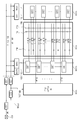
도 1은 본 발명에 따른 반도체 메모리 장치를 보여주는 블록도이다.1 is a block diagram illustrating a semiconductor memory device according to the present invention.
도 2는 본 발명의 제 1 실시예에 따른 도 1에 도시된 메모리 셀 어레이의 일부 및 관련된 주변 회로들을 개략적으로 보여주는 블록도이다.FIG. 2 is a block diagram schematically illustrating a portion of a memory cell array and associated peripheral circuits shown in FIG. 1 according to a first embodiment of the present invention.
도 3은 도 2에 도시된 감지 증폭기를 보여주는 회로도이다.3 is a circuit diagram illustrating the sense amplifier of FIG. 2.
도 4는 본 발명의 제 1 실시예에 따른 반도체 메모리 장치의 웨이퍼 레벨 번-인 테스트 동작을 설명하기 위한 타이밍도이다.4 is a timing diagram illustrating a wafer level burn-in test operation of the semiconductor memory device according to the first embodiment of the present invention.
도 5는 본 발명의 제 2 실시예에 따른 도 1에 도시된 메모리 셀 어레이의 일부 및 관련된 주변 회로들을 개략적으로 보여주는 블록도이다.FIG. 5 is a block diagram schematically illustrating a portion of a memory cell array and associated peripheral circuits shown in FIG. 1 according to a second embodiment of the present invention.
도 6은 본 발명의 제 2 실시예에 따른 반도체 메모리 장치의 웨이퍼 레벨 번-인 테스트 동작을 설명하기 위한 타이밍도이다.6 is a timing diagram illustrating a wafer level burn-in test operation of the semiconductor memory device according to the second embodiment of the present invention.
도 7은 본 발명의 제 3 실시예에 따른 도 1에 도시된 메모리 셀 어레이의 일부 및 관련된 주변 회로들을 개략적으로 보여주는 블록도이다.FIG. 7 is a block diagram schematically illustrating a portion of a memory cell array and associated peripheral circuits shown in FIG. 1 according to a third embodiment of the present invention.
도 8은 본 발명의 제 3 실시예에 따른 반도체 메모리 장치의 웨이퍼 레벨 번-인 테스트 동작을 설명하기 위한 타이밍도이다.8 is a timing diagram illustrating a wafer level burn-in test operation of the semiconductor memory device according to the third embodiment of the present invention.
* 도면의 주요 부분에 대한 부호 설명 *Explanation of symbols on the main parts of the drawings
1100 : 메모리 셀 어레이 1200 : 행 디코더 회로1100: memory cell array 1200: row decoder circuit
1300 : 감지 증폭 회로 1400 : 열 디코더 회로1300: sense amplifier circuit 1400: column decoder circuit
1500 : 감지 증폭기 구동 회로 1600 : 입출력 구동 회로1500: sense amplifier driving circuit 1600: input and output driving circuit
1700 : 번-인 제어 회로1700: burn-in control circuit
본 발명은 반도체 메모리 장치에 관한 것으로, 좀 더 구체적으로는 번-인 테스트 기능을 갖는 반도체 메모리 장치에 관한 것이다.The present invention relates to a semiconductor memory device, and more particularly to a semiconductor memory device having a burn-in test function.
최근, 많은 트랜지스터들이 집적된 반도체 장치들은 웨크스테이션, 개인용 컴퓨터, 휴대용 전자 장치, 등과 같은 다양한 전자 장치들을 위해 사용되어 오고 있다. 반도체 장치를 제조함에 있어서, 신뢰성 테스트 및 결함 스크린을 위해서, 정상 동작 전압보다 높은 전압이 공급 전압으로서 반도체 장치에 인가된 상태에서 반도체 장치를 동작시키고 테스트하기 위한 번-인을 수행할 필요가 있다. 번-인에 의해서 생기는 스트레스때문에, 반도체 장치 내에 포함된 절연막 또는 그와 같은 것에 잠재된 결함 부위가 빠르게 열화되어 드러나게 된다. 따라서, 결함 반도체 장치가 스크린될 수 있다. 알려진 번-인 테스트는 반도체 칩들이 패키지 내에 조립된 후 수행되는 번-인 테스트와, 조립되지 않은 복수의 반도체 칩들을 갖는 웨이퍼 상에서 수행되는 웨이퍼 레벨 번-인(Wafer Level Burn-In: WBI) 테스트를 포함한다.Recently, semiconductor devices incorporating many transistors have been used for various electronic devices such as a wake station, a personal computer, a portable electronic device, and the like. In manufacturing a semiconductor device, it is necessary to perform burn-in for operating and testing the semiconductor device with a voltage higher than the normal operating voltage applied to the semiconductor device as a supply voltage, for the reliability test and the defect screen. Due to the stress caused by burn-in, the defect sites latent in the insulating film or the like contained in the semiconductor device are quickly deteriorated and exposed. Thus, the defective semiconductor device can be screened. Known burn-in tests are a burn-in test performed after semiconductor chips are assembled into a package, and a wafer level burn-in (WBI) test performed on a wafer having a plurality of unassembled semiconductor chips. It includes.
웨이퍼 레벨 번-인 테스트는, 예를 들면, IEDM Tech. Digest (1993, pp.639- 642)에 "WAFER BURN-IN (WBI) TECHNOLOGY FOR RAM'S"라는 제목으로 설명되어 있다. 웨이퍼 레벨 번-인 테스트는 다음과 같은 이점들을 갖는다.Wafer level burn-in tests are described, for example, in IEDM Tech. Digest (1993, pp. 639-642), entitled "WAFER BURN-IN (WBI) TECHNOLOGY FOR RAM'S". Wafer level burn-in test has the following advantages.
첫째로, 반도체 칩이 패키지/몰드 내에 봉인되지 않는다. 그러므로, 패키지/몰드의 견딜 수 있는 온도보다 높은 온도에서 번인을 수행하는 것이 가능하다. 게다가, 번-인 전압이 패드를 통해 외부에서 인가될 수 있다. 번-인 시간을 줄이기 위해 보다 높은 스트레스 전계를 설정하는 것이 가능하다. 둘째로, 웨이퍼 레벨 번-인 테스트는 레이저 트리밍(laser trimming) 또는 그와 같은 것에 의해서 리던던트 비트로 결함 비트를 대체하기 위한 리페어 테스트 이전에 수행된다. 그러므로, 번-인후에 생기는 결함을 리페어하는 것이 가능하며, 수율을 향상시킬 수 있다. 세번째로, 웨이퍼 상에서 검출된 결함을 갖는 반도체 칩의 위치가 체크될 수 있다. 제조 라인으로 결함 정보를 피드백함으로써 웨이퍼 레벨에서 결함 원인을 제거하고 제조 공정을 쉽게 향상시키는 것이 가능하다.First, the semiconductor chip is not sealed in the package / mould. Therefore, it is possible to carry out burn-in at temperatures higher than the tolerable temperature of the package / mould. In addition, the burn-in voltage can be applied externally via the pad. It is possible to set a higher stress field to reduce burn-in time. Secondly, wafer level burn-in tests are performed prior to a repair test to replace defective bits with redundant bits by laser trimming or the like. Therefore, it is possible to repair defects occurring after burn-in, and improve the yield. Third, the position of the semiconductor chip with the detected defect on the wafer can be checked. By feeding back defect information to the manufacturing line, it is possible to eliminate the cause of defects at the wafer level and easily improve the manufacturing process.
DRAM은 하나의 트랜지스터와 하나의 커패시터로 구성된 메모리 셀들을 가지며, 고밀도에 적합한 구조를 갖는다. 그러므로, DRAM은 큰 메모리 용량을 요구하는 개인용 컴퓨터를 위한 메인 메모리로서 사용된다. DRAM에 있어서, 메모리 셀들은 행들 및 열들로 배열되며, 각 셀은 "0" 또는 "1"의 1-비트 정보를 저장한다. 메모리 셀 커패시터의 일 전극은 셀 플레이트로 구성되고 소정 전압(예를 들면, 전원 전압의 1/2)을 공급받는다. 복수의 워드 라인들이 메모리 셀들의 행들을 위해 제공되고, 복수의 비트 라인 쌍들이 메모리 셀들의 열들을 위해 제공된다. 메모리 셀 트랜지스터의 게이트는 대응하는 워드 라인에 연결된다. 메모리 셀 트랜지스터는 대응하는 비트 라인과 메모리 셀 커패시터의 다른 전극(또는 스토리지 전극) 사이에 연결된다.A DRAM has memory cells composed of one transistor and one capacitor, and has a structure suitable for high density. Therefore, DRAM is used as main memory for personal computers that require large memory capacities. In a DRAM, memory cells are arranged in rows and columns, each cell storing one-bit information of "0" or "1". One electrode of the memory cell capacitor is composed of a cell plate and is supplied with a predetermined voltage (eg, 1/2 of a power supply voltage). A plurality of word lines are provided for rows of memory cells, and a plurality of bit line pairs are provided for columns of memory cells. The gate of the memory cell transistor is connected to the corresponding word line. The memory cell transistor is connected between the corresponding bit line and the other electrode (or storage electrode) of the memory cell capacitor.
웨이퍼 레벨 번-인 테스트는, 앞서 언급된 바와 같이, 게이트 산화막의 결함 특성, 워드 라인들의 마이크로 브리지, 비트 라인 브리지, 등과 같은 메모리 장치의 보다 낮은 품질을 잡아내기 위해서 행해진다. 특히, 각 쌍의 비트 라인들 사이에 그리고 비트 라인 쌍들의 인접한 비트 라인들 사이에 생기는 제조 공정 상의 문제점(예를 들면, 비트 라인 브리지)을 스크린하기 위해서 각 쌍의 비트 라인들에 그리고 비트 라인 쌍들의 인접한 비트 라인들에 서로 다른 전압들이 인가되어야 한다. 이를 위해서, 각 쌍의 비트 라인들에 서로 다른 전압들이 인가된 상태에서 웨이퍼 레벨 번-인 테스트가 수행된다. 또한, 비트 라인 쌍들의 인접한 비트 라인들에 서로 다른 전압들이 인가된 상태에서 웨이페 레벨 번-인 테스트가 수행된다. 이러한 웨이퍼 레벨 번-인 테스트 방식은 긴 테스트 시간을 필요로 한다. 결과적으로, 비용 증가의 원인이 된다.Wafer level burn-in tests are conducted to capture the lower quality of the memory device, such as defect characteristics of the gate oxide film, micro bridges of word lines, bit line bridges, and the like, as mentioned above. In particular, in order to screen manufacturing process problems (e.g., bit line bridges) between each pair of bit lines and between adjacent bit lines of the bit line pairs, in each pair of bit lines and in the bit line pairs. Different voltages must be applied to adjacent bit lines. To this end, a wafer level burn-in test is performed with different voltages applied to each pair of bit lines. In addition, a wafer level burn-in test is performed with different voltages applied to adjacent bit lines of the bit line pairs. This wafer level burn-in test approach requires long test times. As a result, the cost increases.
본 발명의 목적은 테스트 시간을 줄일 수 있는 반도체 메모리 장치를 제공하는 것이다.An object of the present invention is to provide a semiconductor memory device that can reduce the test time.
본 발명의 다른 목적은 멀티 테스트 효율을 향상시킬 수 있는 반도체 메모리 장치를 제공하는 것이다.Another object of the present invention is to provide a semiconductor memory device capable of improving multi test efficiency.
본 발명의 또 다른 목적은 단일의 웨이퍼 레벨 번-인 테스트시 각 쌍의 비트 라인들 사이에 그리고 비트 라인 쌍들의 인접한 비트 라인들 사이에 전압차를 동시 에 유발할 수 있는 반도체 메모리 장치를 제공하는 것이다.It is still another object of the present invention to provide a semiconductor memory device capable of simultaneously inducing a voltage difference between each pair of bit lines and between adjacent bit lines of bit line pairs in a single wafer level burn-in test. .
상술한 제반 목적들을 달성하기 위한 본 발명의 특징에 따르면, 반도체 메모리 장치는 복수의 비트 라인 쌍들이 배열된 메모리 블록과; 입출력 라인 쌍들을 구동하는 입출력 구동 회로와; 열 선택 신호들을 발생하는 열 선택 회로와; 감지 증폭 인에이블 신호들을 발생하는 감지 증폭기 구동 회로와; 상기 열 선택 신호들에 응답하여 상기 입출력 라인 쌍들을 상기 비트 라인 쌍들과 전기적으로 연결하고, 상기 감지 증폭 인에이블 신호들에 응답하여 상기 각 쌍의 비트 라인들 사이의 전압차를 감지 증폭하는 감지 증폭 회로와; 하나의 패드에 연결되며, 상기 패드를 통해 입력된 번-인 테스트 신호에 응답하여 상기 입출력 구동 회로, 상기 감지 증폭기 구동 회로, 그리고 상기 열 선택 회로를 제어하는 번-인 제어 회로를 포함하며, 웨이퍼 레벨 번-인 테스트 동작시, 상기 번-인 제어 회로는 상기 각 쌍의 입출력 라인들이 상보 레벨들로 구동된 후 상기 입출력 라인 쌍들이 상기 비트 라인 쌍들과 전기적으로 연결되도록 그리고 상기 각 쌍의 비트 라인들 사이의 전압차가 마지막으로 증폭되도록 상기 입출력 구동 회로, 상기 감지 증폭기 구동 회로, 그리고 상기 열 선택 회로를 제어한다.According to a feature of the present invention for achieving the above objects, a semiconductor memory device comprises a memory block arranged with a plurality of bit line pairs; An input / output drive circuit for driving input / output line pairs; A column select circuit for generating column select signals; Sense amplifier drive circuitry for generating sense amplification enable signals; A sense amplification that electrically couples the input / output line pairs with the bit line pairs in response to the column select signals, and senses and amplifies the voltage difference between the pair of bit lines in response to the sense amplification enable signals. Circuits; A burn-in control circuit connected to one pad, the burn-in control circuit controlling the input / output driving circuit, the sense amplifier driving circuit, and the column selection circuit in response to a burn-in test signal input through the pad; In a level burn-in test operation, the burn-in control circuit is adapted to electrically connect the input / output line pairs to the bit line pairs after the pair of input / output lines are driven to complementary levels and to each of the pair of bit lines. The input / output driving circuit, the sense amplifier driving circuit, and the column selection circuit are controlled so that the voltage difference between them is finally amplified.
이 실시예에 있어서, 상기 번-인 테스트 회로는 상기 번-인 테스트 신호의 활성화에 응답하여 제 1 내지 제 3 번-인 제어 신호들을 발생한다.In this embodiment, the burn-in test circuit generates first to third burn-in control signals in response to activation of the burn-in test signal.
이 실시예에 있어서, 상기 제 1 및 제 2 번-인 제어 신호들은 상기 번-인 테스트 신호의 활성화시 활성화되고, 상기 제 3 번-인 제어 신호는 상기 번-인 테스 트 신호가 활성화되고 소정 지연 시간이 경과한 후 활성화된다.In this embodiment, the first and second burn-in control signals are activated upon activation of the burn-in test signal, and the third burn-in control signal is activated by the burn-in test signal. Activated after the delay has elapsed.
이 실시예에 있어서, 상기 제 1 번-인 제어 신호는 상기 번-인 테스트 신호의 활성화시 활성화되고, 상기 제 2 번-인 제어 신호는 상기 제 1 번-인 제어 신호가 활성화되고 제 1 지연 시간이 경과한 후 활성화되며, 상기 제 3 번-인 제어 신호는 상기 제 2 번-인 테스트 신호가 활성화되고 제 2 지연 시간이 경과한 후 활성화된다.In this embodiment, the first burn-in control signal is activated upon activation of the burn-in test signal, and the second burn-in control signal is activated with the first burn-in control signal and a first delay. After a time elapses, the third burn-in control signal is activated after the second burn-in test signal is activated and a second delay time elapses.
이 실시예에 있어서, 상기 입출력 구동 회로는 상기 제 1 번-인 제어 신호의 활성화에 응답하여 상기 각 쌍의 입출력 라인들을 상보 레벨들로 구동하고, 상기 열 선택 회로는 상기 제 2 번-인 제어 신호의 활성화에 응답하여 상기 열 선택 신호들을 동시에 활성화시키며, 상기 감지 증폭기 구동 회로는 상기 제 3 번-인 제어 신호의 활성화에 응답하여 상기 감지 증폭 인에이블 신호들을 활성화시킨다.In this embodiment, the input / output driving circuit drives the pair of input / output lines at complementary levels in response to the activation of the first burn-in control signal, and the column selection circuit controls the second burn-in control. And simultaneously activate the column select signals in response to activation of the signal, and the sense amplifier drive circuitry activates the sense amplification enable signals in response to activation of the third burn-in control signal.
이 실시예에 있어서, 상기 번-인 테스트 신호가 비활성화될 때, 상기 제 1 번-인 제어 신호는 상기 번-인 테스트 신호가 비활성화되고 제 3 지연 시간이 경과한 후 비활성화된다.In this embodiment, when the burn-in test signal is deactivated, the first burn-in control signal is deactivated after the burn-in test signal is deactivated and a third delay time has elapsed.
이 실시예에 있어서, 상기 감지 증폭기 구동 회로는 상기 제 1 번-인 제어 신호의 활성화에 응답하여 등화 신호들을 비활성화시킨다.In this embodiment, the sense amplifier drive circuitry deactivates equalization signals in response to activation of the first burn-in control signal.
본 발명의 다른 특징에 따르면, 반도체 메모리 장치는 복수의 비트 라인 쌍들이 배열된 메모리 블록과; 하나의 패드에 연결되며, 웨이퍼 레벨 번-인 테스트 동작시 상기 패드를 통해 입력된 번-인 테스트 신호에 응답하여 제 1 내지 제 3 번-인 제어 신호들을 발생하는 번-인 제어 회로와; 상기 제 1 번-인 제어 신호에 응 답하여 각 쌍의 입출력 라인들을 상보 레벨들로 구동하는 입출력 구동 회로와; 상기 제 2 번-인 제어 신호에 응답하여 열 선택 신호들을 동시에 활성화시키는 열 선택 회로와; 상기 제 3 번-인 제어 신호에 응답하여 감지 증폭 인에이블 신호들을 활성화시키는 감지 증폭기 구동 회로와; 그리고 상기 열 선택 신호들에 응답하여 상기 입출력 라인 쌍들을 상기 비트 라인 쌍들과 전기적으로 연결하고, 상기 감지 증폭 인에이블 신호들에 응답하여 상기 각 쌍의 비트 라인들 사이의 전압차를 감지 증폭하는 감지 증폭 회로를 포함하며, 상기 제 1 번-인 제어 신호는 상기 번-인 테스트 신호의 활성화시 활성화되고, 상기 제 2 번-인 제어 신호는 상기 제 1 번-인 제어 신호가 활성화되고 제 1 지연 시간이 경과한 후 활성화되며, 상기 제 3 번-인 제어 신호는 상기 제 2 번-인 테스트 신호가 활성화되고 제 2 지연 시간이 경과한 후 활성화된다.According to another aspect of the present invention, a semiconductor memory device includes a memory block in which a plurality of bit line pairs are arranged; A burn-in control circuit connected to one pad and generating first to third burn-in control signals in response to a burn-in test signal input through the pad during a wafer level burn-in test operation; An input / output driving circuit for driving each pair of input / output lines to complementary levels in response to the first burn-in control signal; A column select circuit for simultaneously activating column select signals in response to the second burn-in control signal; A sense amplifier drive circuit for activating sense amplification enable signals in response to the third burn-in control signal; And sensing to electrically connect the input / output line pairs with the bit line pairs in response to the column select signals, and sense and amplify a voltage difference between the pair of bit lines in response to the sense amplification enable signals. An amplification circuit, wherein the first burn-in control signal is activated upon activation of the burn-in test signal, and the second burn-in control signal is activated with a first delay-in control signal and a first delay. After a time elapses, the third burn-in control signal is activated after the second burn-in test signal is activated and a second delay time elapses.
이 실시예에 있어서, 상기 번-인 제어 회로는 상기 패드를 통해 제공되는 상기 번-인 테스트 신호를 입력받아 상기 제 1 번인 제어 신호를 출력하는 버퍼와; 상기 버퍼의 출력을 상기 제 1 지연 시간만큼 지연시켜 상기 제 2 번-인 제어 신호를 출력하는 제 1 지연 회로와; 그리고 상기 제 1 지연 회로의 출력을 상기 제 2 지연 시간만큼 지연시켜 상기 제 3 번-인 제어 신호를 출력하는 제 2 지연 회로를 포함한다.The burn-in control circuit may include: a buffer configured to receive the burn-in test signal provided through the pad and output the first burn-in control signal; A first delay circuit for delaying the output of the buffer by the first delay time to output the second burn-in control signal; And a second delay circuit outputting the third burn-in control signal by delaying the output of the first delay circuit by the second delay time.
이 실시예에 있어서, 상기 제 1 및 제 2 지연 회로들 각각은 입력 신호의 로우-하이 천이를 지연시키고 상기 입력 신호의 하이-로우 천이를 지연없이 출력한다.In this embodiment, each of the first and second delay circuits delays the low-high transition of the input signal and outputs the high-low transition of the input signal without delay.
이 실시예에 있어서, 상기 번-인 테스트 신호가 비활성화될 때, 상기 제 1 번-인 제어 신호는 상기 번-인 테스트 신호가 비활성화되고 제 3 지연 시간이 경과한 후 비활성화된다.In this embodiment, when the burn-in test signal is deactivated, the first burn-in control signal is deactivated after the burn-in test signal is deactivated and a third delay time has elapsed.
이 실시예에 있어서, 상기 감지 증폭기 구동 회로는 상기 제 1 번-인 제어 신호의 활성화에 응답하여 등화 신호들을 비활성화시킨다.In this embodiment, the sense amplifier drive circuitry deactivates equalization signals in response to activation of the first burn-in control signal.
이 실시예에 있어서, 상기 번-인 제어 회로는 상기 패드를 통해 제공되는 상기 번-인 테스트 신호를 입력받는 버퍼와; 상기 버퍼의 출력을 상기 제 1 지연 시간만큼 지연시켜 상기 제 2 번-인 제어 신호를 출력하는 제 1 지연 회로와; 상기 제 1 지연 회로의 출력을 상기 제 2 지연 시간만큼 지연시켜 상기 제 3 번-인 제어 신호를 출력하는 제 2 지연 회로와; 그리고 상기 버퍼의 출력을 입력받고, 상기 입력된 신호를 상기 제 1 번-인 제어 신호로서 출력하는 제 3 지연 회로를 포함한다.In this embodiment, the burn-in control circuit includes a buffer for receiving the burn-in test signal provided through the pad; A first delay circuit for delaying the output of the buffer by the first delay time to output the second burn-in control signal; A second delay circuit for outputting the third burn-in control signal by delaying the output of the first delay circuit by the second delay time; And a third delay circuit which receives an output of the buffer and outputs the input signal as the first burn-in control signal.
이 실시예에 있어서, 상기 제 1 및 제 2 지연 회로들 각각은 입력 신호의 로우-하이 천이를 지연시키고 상기 입력 신호의 하이-로우 천이를 지연없이 출력하고, 상기 제 3 지연 회로는 입력 신호의 로우-하이 천이를 지연없이 출력하고 상기 입력 신호의 하이-로우 천이를 지연시킨다.In this embodiment, each of the first and second delay circuits delays the low-high transition of the input signal and outputs the high-low transition of the input signal without delay, and the third delay circuit outputs the delay of the input signal. Output a low-high transition without delay and delay the high-low transition of the input signal.
앞의 일반적인 설명 및 다음의 상세한 설명 모두 예시적이라는 것이 이해되어야 하며, 청구된 발명의 부가적인 설명이 제공되는 것으로 여겨져야 한다.It is to be understood that both the foregoing general description and the following detailed description are exemplary, and that additional explanations of the claimed invention are provided.
참조 부호들이 본 발명의 바람직한 실시 예들에 상세히 표시되어 있으며, 그것의 예들이 참조 도면들에 표시되어 있다. 가능한 어떤 경우에도, 동일한 참조 번호들이 동일한 또는 유사한 부분을 참조하기 위해서 설명 및 도면들에 사용된다.Reference numerals are shown in detail in preferred embodiments of the invention, examples of which are shown in the reference figures. In any case, like reference numerals are used in the description and the drawings to refer to the same or like parts.
아래에서, 다이나믹 랜덤 액세스 메모리 장치가 본 발명의 특징 및 기능을 설명하기 위한 한 예로서 사용된다. 하지만, 이 기술 분야에 정통한 사람은 여기에 기재된 내용에 따라 본 발명의 다른 이점들 및 성능을 쉽게 이해할 수 있을 것이다. 본 발명은 다른 실시 예들을 통해 또한, 구현되거나 적용될 수 있을 것이다. 게다가, 상세한 설명은 본 발명의 범위, 기술적 사상 그리고 다른 목적으로부터 상당히 벗어나지 않고 관점 및 응용에 따라 수정되거나 변경될 수 있다.In the following, a dynamic random access memory device is used as an example for explaining the features and functions of the present invention. However, one of ordinary skill in the art will readily appreciate the other advantages and performances of the present invention in accordance with the teachings herein. The present invention may be implemented or applied through other embodiments as well. In addition, the detailed description may be modified or changed according to aspects and applications without departing from the scope, technical spirit and other objects of the present invention.
도 1은 본 발명에 따른 반도체 메모리 장치를 보여주는 블록도이다.1 is a block diagram illustrating a semiconductor memory device according to the present invention.
도 1을 참조하면, 본 발명의 반도체 메모리 장치(1000)는 메모리 셀 어레이(1100)를 포함하며, 메모리 셀 어레이(1100)는 행들 및 열들로 배열된 메모리 셀들을 포함한다. 각 메모리 셀은 1-비트 정보를 저장하며, 잘 알려진 바와 같이, 하나의 트랜지스터와 하나의 커패시터로 구성된다. 메모리 셀 어레이(1100)가 복수의 메모리 블록들로 구성됨은 이 분야의 통상적인 지식을 습득한 자에게 자명하다. 행 디코더 회로(1200)는 행 어드레스에 응답하여 메모리 셀 어레이(1100)의 행들 중 적어도 하나를 선택한다. 감지 증폭 회로(1300)는 읽기 동작시 비트 라인들을 통해 메모리 셀 어레이(1100)로부터 데이터를 감지 증폭하고, 쓰기 동작시 비트 라인들을 통해 메모리 셀 어레이(1100)에 데이터를 기입한다. 열 디코더 회로(1400)는 정상 읽기/쓰기 동작시 열 어드레스에 응답하여 열 선택 신호들(CSLi)을 선택적으로 활성화시키고, 웨이퍼 레벨 번-인 테스트 동작시 번-인 제어 신호(WBI_CSL)에 응답하여 열 어드레스에 관계없이 열 선택 신호들(CLSi)을 동시에 활성화시킨다. 이는 감지 증폭 회로(1300)를 통해 모든 비트 라인 쌍들이 입출력 라인 쌍들(IOj, IOjB) 과 전기적으로 연결되게 한다.Referring to FIG. 1, the
감지 증폭기 구동 회로(1500)는 번-인 제어 신호들(WBI_EQ_IO, WBI_SE)을 공급받고, 정상 읽기/쓰기 동작시 그리고 웨이퍼 레벨 번-인 테스트 동작시 감지 증폭 회로(1300)의 감지 증폭 동작을 제어하기 위한 제어 신호들(예를 들면, PSE, PSEB, PEQIB, PEQJB, PISOI, PISOJ, 등)을 구동한다. 이는 이후 상세히 설명될 것이다. 입출력 구동 회로(1600)는 입출력 라인 쌍들(IOj, IOjB)에 연결되며, 웨이퍼 레벨 번-인 테스트 동작시 번-인 제어 신호(WBI_EQ_IO)에 응답하여 입출력 라인 쌍들(IOj, IOjB)을 구동한다. 특히, 입출력 구동 회로(1600)는 상보적인 전압 레벨을 갖도록 각 쌍의 입출력 라인들을 구동한다. 예를 들면, 한 쌍의 입출력 라인들(IO0, IO0B)은 각각 전원 전압과 접지 전압으로 구동되고, 한 쌍의 입출력 라인들(IO1, IO1B)은 각각 전원 전압과 접지 전압으로 구동되며, 한 쌍의 입출력 라인들(IO2, IO2B)은 각각 전원 전압과 접지 전압으로 구동된다. 이에 반해서, 한 쌍의 입출력 라인들(IO0, IO0B)은 각각 접지 전압과 전원 전압으로 구동되고, 한 쌍의 입출력 라인들(IO1, IO1B)은 각각 접지 전압과 전원 전압으로 구동되며, 한 쌍의 입출력 라인들(IO2, IO2B)은 각각 접지 전압과 전원 전압으로 구동될 수 있다.The sense
계속해서 도 1을 참조하면, 본 발명에 따른 반도체 메모리 장치(1000)는 번-인 제어 회로(1700)를 더 포함하며, 번-인 제어 회로(1700)는 패드(1001)에 연결되며, 웨이퍼 레벨 번-인 테스트 동작시 패드(1001)를 통해 제공되는 번-인 테스트 정보에 응답하여 번-인 제어 신호들(WBI_CSL, WBI_SE, WBI_EQ_IO)을 발생한다. 여기서, 패드(1001)는 리드 프레임과 연결되지 않는 패드이다. 웨이퍼 레벨 번-인 테 스트 동작시 패드(1001)를 통해 번-인 테스트 정보가 입력되면, 번-인 제어 회로(1700)는 번-인 제어 신호들(WBI_CSL, WBI_SE, WBI_EQ_IO)을 발생한다. 특히, 번-인 제어 신호들(WBI_CSL, WBI_SE, WBI_EQ_IO)은 다음과 같은 일련의 동작들이 수행되도록 활성화된다. 각 쌍의 입출력 라인들이 먼저 하이 레벨 및 로우 레벨로 각각 설정되고, 비트 라인들과 입출력 라인들이 그 다음에 연결되며, 각 쌍의 비트 라인들의 전압차가 마지막으로 증폭된다. 이는 이후 상세히 설명될 것이다.1, the
이러한 번-인 테스트 방법에 따르면, 각 쌍의 입출력 라인들을 원하는 상보 레벨들로 각각 설정하고, 비트 라인 쌍들과 입출력 라인 쌍들을 연결함으로써 각 쌍의 비트 라인들 사이에 그리고 비트 라인 쌍들의 인접한 비트 라인들 사이에 전압차를 동시에 유발하는 것이 가능하다.According to this burn-in test method, each pair of input / output lines are set to desired complementary levels, respectively, and the pair of bit line pairs and input / output line pairs are connected between each pair of bit lines and adjacent bit lines of bit line pairs. It is possible to induce a voltage difference between them simultaneously.
도 2는 본 발명의 제 1 실시예에 따른 도 1에 도시된 메모리 셀 어레이의 일부 및 관련된 주변 회로들을 개략적으로 보여주는 블록도이다. 도 2에는 단지 하나의 메모리 블록이 도시되어 있다. 잘 알려진 바와 같이, 감지 증폭 회로(1300)는 메모리 블록들에 의해서 공유되도록 구성된다. 예를 들면, 도 2에 도시된 바와 같이, 하나의 메모리 블록(1100)의 양측에 감지 증폭 블록들(1300L, 1300R)이 각각 배치된다. 감지 증폭 블록(1300L)은 메모리 블록(1100)의 비트 라인 쌍들 중 짝수번 비트 라인 쌍들과 전기적으로 연결되고, 감지 증폭 블록(1300R)은 메모리 블록(1100)의 비트 라인 쌍들 중 홀수번 비트 라인 쌍들과 전기적으로 연결된다. 감지 증폭 블록들(1300L, 1300R) 각각은 대응하는 비트 라인 쌍들과 전기적으로 연결된 감지 증폭기들(1301)로 구성된다.FIG. 2 is a block diagram schematically illustrating a portion of a memory cell array and associated peripheral circuits shown in FIG. 1 according to a first embodiment of the present invention. Only one memory block is shown in FIG. As is well known, the
예시적인 감지 증폭기(1301)를 보여주는 도 3을 참조하면, 감지 증폭기(1301)는 프리챠지 및 등화부들(1301a, 1301b), P-래치 증폭부(1301c), N-래치 증폭부(1301d), 열 게이트부(1301e), 그리고 절연부들(1301f, 1301g)을 포함한다. 제어 신호(PEQIB)가 하이로 활성화될 때, 프리챠지 및 등화부(1301a)는 대응하는 메모리 블록의 비트 라인들(BL0, BLB0)을 프리챠지 전압(VBL)으로 프리챠지 및 등화한다. 제어 신호(PEQJB)가 하이로 활성화될 때, 프리챠지 및 등화부(1301b)는 대응하는 메모리 블록의 비트 라인들(BL0, BLB0)을 프리챠지 전압(VBL)으로 프리챠지 및 등화한다. P-래치 및 N-래치 증폭부들(1301c, 1301d)는 선택된 메모리 블록의 비트 라인들(BL0, BLB0) 사이의 전압차를 감지 증폭한다. 예를 들면, 비트 라인(BL0)의 전압이 비트 라인(BLB0)의 전압보다 높은 경우, P-래치 증폭부(1301c)는 비트 라인(BL0)의 전압을 제어 신호(SE)의 전압(예를 들면, 하이-레벨 전압)으로 증폭하고 N-래치 증폭부(1301d)는 비트 라인(BLB0)의 전압을 제어 신호(SEB)의 전압(예를 들면, 로우-레벨 전압)으로 증폭한다. 열 게이트부(1301e)는 열 선택 신호(CSL0)에 응답하여 선택된 메모리 블록의 비트 라인들(BL0, BLB0)을 대응하는 입출력 라인들(IO0, IOB0)과 전기적으로 연결하거나 절연시킨다. 절연부(1301f)는 제어 신호(PISOI)에 응답하여 대응하는 메모리 블록의 비트 라인들(BL0, BLB0)을 증폭부들(1301c, 1301d)과 전기적으로 연결하거나 절연시킨다. 절연부(1301g)는 제어 신호(PISOJ)에 응답하여 대응하는 메모리 블록의 비트 라인들(BL0, BLB0)을 증폭부들(1301c, 1301d)과 전기적으로 연결하거나 절연시킨다.Referring to FIG. 3, which shows an
다시 도 2를 참조하면, 감지 증폭기 구동부(1500L)는 감지 증폭 블록(1300L) 의 감지 증폭기들(1301)에 공급되는 제어 신호들(예를 들면, PISOI, PISOJ, SE, SEB, PEQIB, PEQJB)을 구동하고, 감지 증폭기 구동부(1500R)는 감지 증폭 블록(1300R)의 감지 증폭기들(1301)에 공급되는 제어 신호들(예를 들면, PISOI, PISOJ, SE, SEB, PEQIB, PEQJB)을 구동한다. 감지 증폭 블록(1300L)을 통해 입출력 라인들이 배치되고, 입출력 라인 쌍들(IOx, IOBx)은 입출력 구동부(1600L)에 의해서 구동된다. 마찬가지로, 감지 증폭 블록(1300R)을 통해 입출력 라인 쌍들(IOy, IOBy)이 배치되고, 입출력 라인들(IOj,IOBj)은 입출력 구동부(1600R)에 의해서 구동된다. 열 선택 회로(1400)는 정상 동작시 열 어드레스에 따라 열 선택 신호들(CSL0-CSLm)을 선택적으로 구동한다.Referring back to FIG. 2, the
번-인 제어 회로(1700)는 패드(1001)에 연결되며, 웨이퍼 레벨 번-인 테스트 동작시 패드(1001)에 공급되는 번-인 테스트 정보(WBI)에 응답하여 번-인 제어 신호들(WBI_SE, WBI_EQ_IO, WBI_CSL)을 발생한다. 번-인 제어 회로(1700)는 버퍼부(1702) 및 소정의 지연 시간(△t0)을 갖는 지연부(1704)로 구성된다. 여기서, 지연부(1704)는 입력 신호의 로우-하이 천이를 정해진 시간만큼 지연시키고 입력 신호의 하이-로우 천이를 지연없이 출력한다. 열 디코더 회로(1400)는 번-인 제어 신호(WBI_CSL)가 활성화될 때 열 선택 신호들(CSLi)을 동시에 활성화시킨다. 입출력 구동부들(1600L, 1600R)은 번-인 제어 신호(WBI_EQ_IO)가 활성화될 때 입출력 라인들을 하이-레벨 전압과 로우-레벨 전압으로 각각 구동한다. 감지 증폭기 구동부들(1500L, 1500R)은 번-인 제어 신호(WBI_EQ_IO)가 활성화될 때 감지 증폭기의 제어 신호들을 활성화/비활성화시킨다. 특히, 웨이퍼 레벨 번-인 테스트 동작시, 번-인 제어 신호들(WBI_EQ_IO, WBI_CSL, WBI_SE)의 활성화 순서는 입출력 라인들의 구동 이후에 비트 라인들과 입출력 라인들이 연결되고 비트 라인들이 증폭되도록 결정될 것이다.The burn-in
도 4는 본 발명의 제 1 실시예에 따른 반도체 메모리 장치의 웨이퍼 레벨 번-인 테스트 동작을 설명하기 위한 타이밍도이다. 이하, 반도체 메모리 장치의 웨이퍼 레벨 번-인 테스트 동작이 참조 도면들에 의거하여 상세히 설명될 것이다. 본 발명에 따른 반도체 메모리 장치는 각 쌍의 비트 라인들 사이에 그리고 비트 라인 쌍들의 인접한 비트 라인들 사이에 동시에 스트레스를 가할 수 있는 웨이퍼 레벨 번-인 테스트 동작을 수행하기에 적합하다. 좀 더 구체적으로 설명하면 다음과 같다.4 is a timing diagram illustrating a wafer level burn-in test operation of the semiconductor memory device according to the first embodiment of the present invention. Hereinafter, the wafer level burn-in test operation of the semiconductor memory device will be described in detail based on the reference drawings. The semiconductor memory device according to the present invention is suitable for performing a wafer level burn-in test operation that can simultaneously stress between each pair of bit lines and between adjacent bit lines of the bit line pairs. More specifically, it is as follows.
패드(1001)에 인가되는 번-인 테스트 신호(WBI)가 하이 레벨로 활성화되면, 먼저, 번-인 제어 신호들(WBI_EQ_IO, WBI_CSL)이 하이로 활성화된다. 열 디코더 회로(1400)는 번-인 제어 신호(WBI_CSL)의 활성화에 응답하여 모든 열 선택 신호들(CSLi)을 동시에 활성화시킨다. 입출력 구동부들(1600L, 1600R)은 번-인 제어 신호(WBI_EQ_IO)의 활성화에 응답하여 각 쌍의 입출력 라인들(IOj, IOBj)을 하이-레벨 전압 및 로우-레벨 전압으로 (또는 로우-레벨 전압 및 하이-레벨 전압으로) 각각 구동한다. 감지 증폭기 구동부들(1500L, 1500R) 각각은 번-인 제어 신호(WBI_EQ_IO)의 활성화에 응답하여 제어 신호들(PEQIB, PEQJB)을 로우로 비활성화시킨다. 웨이퍼 레벨 번-인 테스트 동작시, 감지 증폭기들(1301)에 인가되는 제어 신호들(PISOI, PISOJ)은 하이 레벨로 유지된다. 설명의 편의상, 하나의 감지 증폭기 를 기준으로 번-인 테스트 동작이 설명될 것이다.When the burn-in test signal WBI applied to the
도 3에 있어서, 열 선택 신호(CSL0)가 활성화됨에 따라, 입출력 라인 쌍(IO0, IOB0)은 열 게이트부(1301e)를 통해 각 메모리 블록의 비트 라인 쌍(BL0, BLB0)과 전기적으로 연결된다. 도 4에 도시된 바와 같이, 한 쌍의 입출력 라인들(IO0, IOB0)은 번-인 제어 신호(WBI_EQ_IO)의 활성화시 입출력 구동 회로(1600)를 통해 로우-레벨 전압 및 하이-레벨 전압으로 각각 구동된다. 이와 동시에, 입출력 라인 쌍(IO0, IOB0)이 열 게이트부(1301e)를 통해 각 메모리 블록의 비트 라인 쌍(BL0, BLB0)과 전기적으로 연결되어 있기 때문에, 도 4에 도시된 바와 같이, 비트 라인들(BL0, BLB0) 사이에 전압차가 생기기 시작한다. 지연부(1704)의 정해진 지연 시간 후에 번-인 제어 신호(WBI_SE)가 하이로 활성화된다.In FIG. 3, as the column select signal CSL0 is activated, the input / output line pairs IO0 and IOB0 are electrically connected to the bit line pairs BL0 and BLB0 of each memory block through the
감지 증폭기 구동 회로(1500)는 번-인 제어 신호(WBI_SE)의 활성화에 응답하여 제어 신호들(SE, SEB)을 하이-레벨 전압 및 로우-레벨 전압으로 각각 구동한다. 이는 P-래치 및 N-래치 증폭부들(1301c, 1301d)을 통해 비트 라인들(BL0, BLB0)이 로우-레벨 전압 및 하이-레벨 전압으로 각각 증폭되게 한다. 따라서, 각 쌍의 비트 라인들 사이에 스트레스가 가해진다. 게다가, 각 쌍의 비트 라인들이 로우-레벨 전압 및 하이-레벨 전압로 설정됨에 따라, 비트 라인 쌍들의 인접한 비트라인들 사이에도 스트레스가 가해진다. 예를 들면, 앞서의 설명에 따르면, 비트 라인들(BL0, BLB0)이 로우-레벨 전압 및 하이-레벨 전압로 각각 설정되고, 비트 라인들(BL1, BLB1)이 로우-레벨 전압 및 하이-레벨 전압로 각각 설정된다. 비트 라인(BLB0)이 하이-레벨 전압으로 설정되고 비트 라인(BL1)이 로우-레벨 전압으로 설정되기 때문 에, 비트 라인 쌍들의 인접한 비트 라인들 사이에 전압차가 생긴다.The sense
패드(1001)에 인가되는 웨이퍼 레벨 번-인 신호(WBI)가 로우로 비활성화됨에 따라, 번-인 제어 신호들(WBI_EQ_IO, WBI_SE, WBI_CSL)은 로우로 비활성화된다. 즉, 웨이퍼 레벨 번-인 테스트 동작이 종료된다.As the wafer level burn-in signal WBI applied to the
이상의 설명에서 알 수 있듯이, 단지 하나의 패드만을 이용하여 웨이퍼 레벨 번-인 테스트 동작이 수행된다. 이는 하나의 테스터를 통해 보다 많은 반도체 메모리 장치들을 동시에 테스트할 수 있음을 의미한다. 즉, 멀티 테스팅 효율이 향상된다. 게다가, 각 쌍의 비트 라인들 사이에 그리고 비트 라인 쌍들의 인접한 비트 라인들 사이에 스트레스를 동시에 가할 수 있기 때문에, 전반적인 테스트 시간을 줄이는 것이 가능하다.As can be seen from the above description, a wafer level burn-in test operation is performed using only one pad. This means that one semiconductor tester can test more semiconductor memory devices at the same time. That is, the multi testing efficiency is improved. In addition, since stress can be applied simultaneously between each pair of bit lines and between adjacent bit lines of the bit line pairs, it is possible to reduce the overall test time.
도 5는 본 발명의 제 2 실시예에 따른 도 1에 도시된 메모리 셀 어레이의 일부 및 관련된 주변 회로들을 개략적으로 보여주는 블록도이다. 도 5에 있어서, 도 2에 도시된 구성 요소들과 동일한 기능을 갖는 구성 요소들은 동일한 참조 번호로 표기되며, 그것에 대한 설명은 생략된다.FIG. 5 is a block diagram schematically illustrating a portion of a memory cell array and associated peripheral circuits shown in FIG. 1 according to a second embodiment of the present invention. In FIG. 5, components having the same functions as the components shown in FIG. 2 are denoted by the same reference numerals, and description thereof is omitted.
도 5를 참조하면, 번-인 제어 회로(1700a)는 패드(1001)에 연결되며, 웨이퍼 레벨 번-인 테스트 동작시 패드(1001)에 공급되는 테스트 정보(WBI)에 응답하여 번-인 제어 신호들(WBI_SE, WBI_EQ_IO, WBI_CSL)을 발생한다. 번-인 제어 회로(1700a)는 버퍼부(1712), 제 1 지연 시간(△t1)을 갖는 지연부(1714), 그리고 제 2 지연 시간(△t0)을 갖는 지연부(1716)로 구성된다. 여기서, 지연부들(1714, 1716) 각각은 입력 신호의 로우-하이 천이를 정해진 시간만큼 지연시키고 입력 신호의 하 이-로우 천이를 지연없이 출력한다. 버퍼부(1712)는 패드(1001)를 통해 입력되는 번-인 테스트 신호(WBI)에 응답하여 번-인 제어 신호(WBI_EQ_IO)를 출력하고, 지연부(1714)는 버퍼(1712)의 출력을 제 1 지연 시간(△t1)만큼 지연시키고, 지연된 신호를 번-인 제어 신호(WBI_CSL)로서 출력하며, 지연부(1716)는 지연부(1714)의 출력을 제 2 지연 시간(△t0)만큼 지연시키고, 지연된 신호를 번-인 제어 신호(WBI_SE)로서 출력한다.Referring to FIG. 5, the burn-in
도 6은 본 발명의 제 2 실시예에 따른 반도체 메모리 장치의 웨이퍼 레벨 번-인 테스트 동작을 설명하기 위한 타이밍도이다. 이하, 반도체 메모리 장치의 웨이퍼 레벨 번-인 테스트 동작이 참조 도면들에 의거하여 상세히 설명될 것이다. 본 발명에 따른 반도체 메모리 장치는 각 쌍의 비트 라인들 사이에 그리고 비트 라인 쌍들의 인접한 비트 라인들 사이에 동시에 스트레스를 가할 수 있는 웨이퍼 레벨 번-인 테스트 동작을 수행하기에 적합하다. 좀 더 구체적으로 설명하면 다음과 같다.6 is a timing diagram illustrating a wafer level burn-in test operation of the semiconductor memory device according to the second embodiment of the present invention. Hereinafter, the wafer level burn-in test operation of the semiconductor memory device will be described in detail based on the reference drawings. The semiconductor memory device according to the present invention is suitable for performing a wafer level burn-in test operation that can simultaneously stress between each pair of bit lines and between adjacent bit lines of the bit line pairs. More specifically, it is as follows.
패드(1001)에 인가되는 번-인 테스트 신호(WBI)가 하이 레벨로 활성화되면, 먼저, 번-인 제어 신호(WBI_EQ_IO)가 하이로 활성화된다. 입출력 구동부들(1600L, 1600R)은 번-인 제어 신호(WBI_EQ_IO)의 활성화에 응답하여 각 쌍의 입출력 라인들(IOj, IOBj)을 하이-레벨 전압 및 로우-레벨 전압으로 (또는 로우-레벨 전압 및 하이-레벨 전압으로) 각각 구동한다. 감지 증폭기 구동부들(1500L, 1500R) 각각은 번-인 제어 신호(WBI_EQ_IO)의 활성화에 응답하여 제어 신호들(PEQIB, PEQJB)을 로우로 비활성화시킨다. 웨이퍼 레벨 번-인 테스트 동작시, 감지 증폭기들(1301)에 인 가되는 제어 신호들(PISOI, PISOJ)은 하이 레벨로 유지된다. 번-인 제어 신호(WBI_EQ_IO)가 활성화되고 소정의 시간 즉, 제 1 지연 시간(△t1)이 경과한 후, 도 6에 도시된 바와 같이, 번-인 제어 신호(WBI_CSL)가 하이로 활성화된다. 열 디코더 회로(1400)는 번-인 제어 신호(WBI_CSL)의 활성화에 응답하여 모든 열 선택 신호들(CSLi)을 동시에 활성화시킨다. 설명의 편의상, 하나의 감지 증폭기를 기준으로 동작이 설명될 것이다.When the burn-in test signal WBI applied to the
도 3에 있어서, 열 선택 신호(CSL0)가 활성화됨에 따라, 입출력 라인 쌍(IO0, IOB0)은 열 게이트부(1301e)를 통해 각 메모리 블록의 비트 라인 쌍(BL0, BLB0)과 전기적으로 연결된다. 도 6에 도시된 바와 같이, 한 쌍의 입출력 라인들(IO0, IOB0)은 번-인 제어 신호(WBI_EQ_IO)의 활성화시 입출력 구동 회로(1600)를 통해 로우-레벨 전압 및 하이-레벨 전압으로 각각 구동된다. 제 1 지연 시간(△t1)이 경과한 후, 입출력 라인 쌍(IO0, IOB0)이 열 게이트부(1301e)를 통해 각 메모리 블록의 비트 라인 쌍(BL0, BLB0)과 전기적으로 연결되어 있기 때문에, 도 6에 도시된 바와 같이, 비트 라인들(BL0, BLB0) 사이에 전압차가 생기기 시작한다. 번-인 제어 신호(WBI_CSL)가 활성화되고 지연부(1716)의 정해진 지연 시간(△t0)이 경과 후에 번-인 제어 신호(WBI_SE)가 하이로 활성화된다.In FIG. 3, as the column select signal CSL0 is activated, the input / output line pairs IO0 and IOB0 are electrically connected to the bit line pairs BL0 and BLB0 of each memory block through the
감지 증폭기 구동 회로(1500)는 번-인 제어 신호(WBI_SE)의 활성화에 응답하여 제어 신호들(SE, SEB)을 하이-레벨 전압 및 로우-레벨 전압으로 각각 구동한다. 이는 P-래치 및 N-래치 증폭부들(1301c, 1301d)을 통해 비트 라인들(BL0, BLB0)이 로우-레벨 전압 및 하이-레벨 전압으로 각각 증폭되게 한다. 따라서, 각 쌍의 비트 라인들 사이에 스트레스가 가해진다. 게다가, 각 쌍의 비트 라인들이 로우-레벨 전압 및 하이-레벨 전압로 설정됨에 따라, 비트 라인 쌍들의 인접한 비트라인들 사이에도 스트레스가 가해진다. 예를 들면, 앞서의 설명에 따르면, 비트 라인들(BL0, BLB0)이 로우-레벨 전압 및 하이-레벨 전압로 각각 설정되고, 비트 라인들(BL1, BLB1)이 로우-레벨 전압 및 하이-레벨 전압로 각각 설정된다. 비트 라인(BLB0)이 하이-레벨 전압으로 설정되고 비트 라인(BL1)이 로우-레벨 전압으로 설정되기 때문에, 비트 라인 쌍들의 인접한 비트 라인들 사이에 전압차가 생긴다.The sense
패드(1001)에 인가되는 웨이퍼 레벨 번-인 신호(WBI)가 로우로 비활성화됨에 따라, 번-인 제어 신호들(WBI_EQ_IO, WBI_SE, WBI_CSL)은 로우로 비활성화된다. 즉, 웨이퍼 레벨 번-인 테스트 동작이 종료된다.As the wafer level burn-in signal WBI applied to the
제 1 실시예와 마찬가지로, 제 2 실시예에 따른 반도체 메모리 장치는 단지 하나의 패드만을 이용하여 웨이퍼 레벨 번-인 테스트 동작을 수행한다. 이는 하나의 테스터를 통해 보다 많은 반도체 메모리 장치들을 동시에 테스트할 수 있음을 의미한다. 각 쌍의 비트 라인들 사이에 그리고 비트 라인 쌍들의 인접한 비트 라인들 사이에 스트레스를 동시에 가할 수 있기 때문에, 전반적인 테스트 시간을 줄이는 것이 가능하다.Like the first embodiment, the semiconductor memory device according to the second embodiment performs wafer level burn-in test operation using only one pad. This means that one semiconductor tester can test more semiconductor memory devices at the same time. Since stress can be simultaneously applied between each pair of bit lines and between adjacent bit lines of the bit line pairs, it is possible to reduce the overall test time.
도 7은 본 발명의 제 3 실시예에 따른 도 1에 도시된 메모리 셀 어레이의 일부 및 관련된 주변 회로들을 개략적으로 보여주는 블록도이다. 도 7에 있어서, 도 2에 도시된 구성 요소들과 동일한 기능을 갖는 구성 요소들은 동일한 참조 번호로 표기되며, 그것에 대한 설명은 생략된다.FIG. 7 is a block diagram schematically illustrating a portion of a memory cell array and associated peripheral circuits shown in FIG. 1 according to a third embodiment of the present invention. In FIG. 7, components having the same functions as those shown in FIG. 2 are denoted by the same reference numerals, and description thereof is omitted.
도 7을 참조하면, 번-인 제어 회로(1700b)는 패드(1001)에 연결되며, 웨이퍼 레벨 번-인 테스트 동작시 패드(1001)에 공급되는 번-인 테스트 신호(WBI)에 응답하여 번-인 제어 신호들(WBI_SE, WBI_EQ_IO, WBI_CSL)을 발생한다. 번-인 제어 회로(1700b)는 버퍼부(1722), 제 1 지연 시간(△t1)을 갖는 지연부(1724), 제 2 지연 시간(△t0)을 갖는 지연부(1726), 그리고 제 3 지연 시간(△t2)을 갖는 지연부(1726)로 구성된다. 버퍼부(1722)는 패드(1001)를 통해 입력되는 번-인 테스트 신호(WBI)를 입력받고, 지연부(1724)는 버퍼(1722)의 출력을 제 1 지연 시간(△t1)만큼 지연시키고, 지연된 신호를 번-인 제어 신호(WBI_CSL)로서 출력하며, 지연부(1726)는 지연부(1724)의 출력을 제 2 지연 시간(△t0)만큼 지연시키고, 지연된 신호를 번-인 제어 신호(WBI_SE)로서 출력한다. 지연부들(1724, 1726) 각각은 입력 신호의 로우-하이 천이를 정해진 시간만큼 지연시키고 입력 신호의 하이-로우 천이를 지연없이 출력한다.Referring to FIG. 7, the burn-in
지연부들(1724, 1726)과 달리, 지연부(1728)는 버퍼(1722)의 출력이 로우-하이 천이를 가질 때 지연 없이 버퍼(1722)의 출력을 번-인 제어 신호(WBI_EQ_IO)로서 출력한다. 버퍼(1722)의 출력이 하이-로우 천이를 가질 때, 지연부(1728)는 버퍼 출력의 하이-로우 천이를 제 3 지연 시간(△t2)만큼 지연시킨다. 즉, 번-인 제어 신호(WBI_EQ_IO)의 하이-로우 천이는 버퍼 출력이 하이-로우 천이를 갖고 소정 시간 즉, 제 3 지연 시간(△t2)이 경과한 후 생긴다.Unlike the
도 8은 본 발명의 제 3 실시예에 따른 반도체 메모리 장치의 웨이퍼 레벨 번-인 테스트 동작을 설명하기 위한 타이밍도이다. 이하, 반도체 메모리 장치의 웨이 퍼 레벨 번-인 테스트 동작이 참조 도면들에 의거하여 상세히 설명될 것이다. 본 발명에 따른 반도체 메모리 장치는 각 쌍의 비트 라인들 사이에 그리고 비트 라인 쌍들의 인접한 비트 라인들 사이에 동시에 스트레스를 가할 수 있는 웨이퍼 레벨 번-인 테스트 동작을 수행하기에 적합하다. 좀 더 구체적으로 설명하면 다음과 같다.8 is a timing diagram illustrating a wafer level burn-in test operation of the semiconductor memory device according to the third embodiment of the present invention. Hereinafter, the wafer level burn-in test operation of the semiconductor memory device will be described in detail with reference to the accompanying drawings. The semiconductor memory device according to the present invention is suitable for performing a wafer level burn-in test operation that can simultaneously stress between each pair of bit lines and between adjacent bit lines of the bit line pairs. More specifically, it is as follows.
패드(1001)에 인가되는 번-인 테스트 신호(WBI)가 하이 레벨로 활성화되면, 먼저, 지연부(1728)를 통해 번-인 제어 신호(WBI_EQ_IO)가 하이로 활성화된다. 앞서 언급된 바와 같이, 버퍼 출력의 로우-하이 천이는 지연부(1728)에 의해서 지연되지 않는다. 입출력 구동부들(1600L, 1600R)은 번-인 제어 신호(WBI_EQ_IO)의 활성화에 응답하여 각 쌍의 입출력 라인들(IOj, IOBj)을 하이-레벨 전압 및 로우-레벨 전압으로 (또는 로우-레벨 전압 및 하이-레벨 전압으로) 각각 구동한다. 감지 증폭기 구동부들(1500L, 1500R) 각각은 번-인 제어 신호(WBI_EQ_IO)의 활성화에 응답하여 제어 신호들(PEQIB, PEQJB)을 로우로 비활성화시킨다. 웨이퍼 레벨 번-인 테스트 동작시, 감지 증폭기들(1301)에 인가되는 제어 신호들(PISOI, PISOJ)은 하이 레벨로 유지된다. 번-인 제어 신호(WBI_EQ_IO)가 활성화되고 소정의 시간 즉, 제 1 지연 시간(△t1)이 경과한 후, 도 8에 도시된 바와 같이, 번-인 제어 신호(WBI_CSL)가 활성화된다. 열 디코더 회로(1400)는 번-인 제어 신호(WBI_CSL)의 활성화에 응답하여 모든 열 선택 신호들(CSLi)을 동시에 활성화시킨다. 설명의 편의상, 하나의 감지 증폭기를 기준으로 번-인 테스트 동작이 설명될 것이다.When the burn-in test signal WBI applied to the
도 3에 있어서, 열 선택 신호(CSL0)이 활성화됨에 따라, 입출력 라인 쌍 (IO0, IOB0)은 열 게이트부(1301e)를 통해 각 메모리 블록의 비트 라인 쌍(BL0, BLB0)과 전기적으로 연결된다. 도 8에 도시된 바와 같이, 한 쌍의 입출력 라인들(IO0, IOB0)은 번-인 제어 신호(WBI_EQ_IO)의 활성화시 입출력 구동 회로(1600)를 통해 로우-레벨 전압 및 하이-레벨 전압으로 각각 구동된다. 제 1 지연 시간(△t1)이 경과한 후, 입출력 라인 쌍(IO0, IOB0)이 열 게이트부(1301e)를 통해 각 메모리 블록의 비트 라인 쌍(BL0, BLB0)과 전기적으로 연결되어 있기 때문에, 도 8에 도시된 바와 같이, 비트 라인들(BL0, BLB0) 사이에 전압차가 생기기 시작한다. 번-인 제어 신호(WBI_CSL)가 활성화되고 지연부(1726)의 정해진 지연 시간(△t0)이 경과 후에 번-인 제어 신호(WBI_SE)가 하이로 활성화된다.3, as the column select signal CSL0 is activated, the input / output line pairs IO0 and IOB0 are electrically connected to the bit line pairs BL0 and BLB0 of each memory block through the
감지 증폭기 구동 회로(1500)는 번-인 제어 신호(WBI_SE)의 활성화에 응답하여 제어 신호들(SE, SEB)을 하이-레벨 전압 및 로우-레벨 전압으로 각각 구동한다. 이는 P-래치 및 N-래치 증폭부들(1301c, 1301d)을 통해 비트 라인들(BL0, BLB0)이 로우-레벨 전압 및 하이-레벨 전압으로 각각 증폭되게 한다. 따라서, 각 쌍의 비트 라인들 사이에 스트레스가 가해진다. 게다가, 각 쌍의 비트 라인들이 로우-레벨 전압 및 하이-레벨 전압로 설정됨에 따라, 비트 라인 쌍들의 인접한 비트라인들 사이에도 스트레스가 가해진다. 예를 들면, 앞서의 설명에 따르면, 비트 라인들(BL0, BLB0)이 로우-레벨 전압 및 하이-레벨 전압로 각각 설정되고, 비트 라인들(BL1, BLB1)이 로우-레벨 전압 및 하이-레벨 전압로 각각 설정된다. 비트 라인(BLB0)이 하이-레벨 전압으로 설정되고 비트 라인(BL1)이 로우-레벨 전압으로 설정되기 때문에, 비트 라인 쌍들의 인접한 비트 라인들 사이에 전압차가 생긴다.The sense
패드(1001)에 인가되는 번-인 테스트 신호(WBI)가 로우로 비활성화될 때, 제 1 실시예와 달리, 번-인 제어 신호(WBI_EQ_IO)는 번-인 테스트 신호(WBI)가 로우로 비활성화되고 일정 지연 시간(△t2)이 경과한 후에 로우로 비활성화된다. 즉, 열 선택 신호(CSLi)가 비활성화되고 지연 시간(△t2)이 경과한 후에 감지 증폭기 구동 회로(1500) 및 입출력 구동 회로(1600)가 비활성화된다. 즉, 웨이퍼 레벨 번-인 테스트 동작이 종료된다.When the burn-in test signal WBI applied to the
제 1 및 제 2 실시예들과 마찬가지로, 제 3 실시예에 따른 반도체 메모리 장치는 단지 하나의 패드만을 이용하여 웨이퍼 레벨 번-인 테스트 동작을 수행한다. 이는 하나의 테스터를 통해 보다 많은 반도체 메모리 장치들을 동시에 테스트할 수 있음을 의미한다. 각 쌍의 비트 라인들 사이에 그리고 비트 라인 쌍들의 인접한 비트 라인들 사이에 스트레스를 동시에 가할 수 있기 때문에, 전반적인 테스트 시간을 줄이는 것이 가능하다.Similar to the first and second embodiments, the semiconductor memory device according to the third embodiment performs a wafer level burn-in test operation using only one pad. This means that one semiconductor tester can test more semiconductor memory devices at the same time. Since stress can be simultaneously applied between each pair of bit lines and between adjacent bit lines of the bit line pairs, it is possible to reduce the overall test time.
본 발명의 범위 또는 기술적 사상을 벗어나지 않고 본 발명의 구조가 다양하게 수정되거나 변경될 수 있음은 이 분야에 숙련된 자들에게 자명하다. 예를 들면, 각 쌍의 입출력 라인들은 로우-레벨 전압 및 하이-레벨 전압으로 구동되거나 하이-레벨 전압 및 로우-레벨 전압으로 구동될 수 있다. 이는 입출력 구동 회로(1600)에 선택 정보를 제공함으로써 쉽게 달성될 수 있다. 선택 정보는 웨이퍼 레벨 번-인 테스트 동작시 별도의 패드를 통해 테스터에 의해서 제공되거나, 잘 알려진 비밀키 입력 방식에 따라 패드(1001)를 통해 입력될 수 있다. 후자의 경우, 패드(1001)에는 비밀키 입력 검출 기능을 갖는 잘 알려진 회로가 연결되어야 한다. 또한, 감지 증폭기(1301)에 공급되는 프리챠지 전압(VBL)은 잘 알려진 프리챠지 전압 발생기를 통해 내부적을 생성되거나, 별도의 패드를 통해 테스터에 의해서 직접 공급될 수 있다. 이에 반해서, 비트 라인들 사이에 스트레스가 가해지는 웨이퍼 레벨 번-인 테스트 동작시, 프리챠지 전압(VBL)이 사용되지 않을 수도 있다. 상술한 내용을 고려하여 볼 때, 만약 본 발명의 수정 및 변경이 아래의 청구항들 및 동등물의 범주 내에 속한다면, 본 발명이 이 발명의 변경 및 수정을 포함하는 것으로 여겨진다.It will be apparent to those skilled in the art that the structure of the present invention may be variously modified or changed without departing from the scope or spirit of the present invention. For example, each pair of input / output lines may be driven with a low-level voltage and a high-level voltage or may be driven with a high-level voltage and a low-level voltage. This can be easily accomplished by providing selection information to the input /
상술한 바와 같이, 본 발명에 따른 반도체 메모리 장치는 단지 하나의 패드만을 이용하여 웨이퍼 레벨 번-인 테스트 동작을 수행한다. 이는 하나의 테스터를 통해 보다 많은 반도체 메모리 장치들을 동시에 테스트할 수 있음을 의미한다. 각 쌍의 비트 라인들 사이에 그리고 비트 라인 쌍들의 인접한 비트 라인들 사이에 스트레스를 동시에 가할 수 있기 때문에, 전반적인 테스트 시간을 줄이는 것이 가능하다.As described above, the semiconductor memory device according to the present invention performs a wafer level burn-in test operation using only one pad. This means that one semiconductor tester can test more semiconductor memory devices at the same time. Since stress can be simultaneously applied between each pair of bit lines and between adjacent bit lines of the bit line pairs, it is possible to reduce the overall test time.
Claims (14)
Priority Applications (1)
| Application Number | Priority Date | Filing Date | Title |
|---|---|---|---|
| KR1020050075192A KR100749552B1 (en) | 2005-08-17 | 2005-08-17 | Semiconductor memory device can reduce burn-in test time |
Applications Claiming Priority (1)
| Application Number | Priority Date | Filing Date | Title |
|---|---|---|---|
| KR1020050075192A KR100749552B1 (en) | 2005-08-17 | 2005-08-17 | Semiconductor memory device can reduce burn-in test time |
Publications (2)
| Publication Number | Publication Date |
|---|---|
| KR20070020857A KR20070020857A (en) | 2007-02-22 |
| KR100749552B1 true KR100749552B1 (en) | 2007-08-14 |
Family
ID=41631565
Family Applications (1)
| Application Number | Title | Priority Date | Filing Date |
|---|---|---|---|
| KR1020050075192A Expired - Lifetime KR100749552B1 (en) | 2005-08-17 | 2005-08-17 | Semiconductor memory device can reduce burn-in test time |
Country Status (1)
| Country | Link |
|---|---|
| KR (1) | KR100749552B1 (en) |
Citations (5)
| Publication number | Priority date | Publication date | Assignee | Title |
|---|---|---|---|---|
| JPH06223595A (en) * | 1992-09-30 | 1994-08-12 | Sgs Thomson Microelectron Inc | Stress test of memory array in integrated circuit |
| KR970076882A (en) * | 1996-05-17 | 1997-12-12 | 김광호 | Burn-in stress circuit of semiconductor memory device |
| JP2001176296A (en) | 1999-12-10 | 2001-06-29 | Fujitsu Ltd | Dynamic memory device for stress testing |
| JP2001236798A (en) | 2000-02-18 | 2001-08-31 | Fujitsu Ltd | Semiconductor memory device and stress voltage setting method |
| KR20030052396A (en) * | 2001-12-21 | 2003-06-27 | 주식회사 하이닉스반도체 | Semiconductor memory test device |
-
2005
- 2005-08-17 KR KR1020050075192A patent/KR100749552B1/en not_active Expired - Lifetime
Patent Citations (5)
| Publication number | Priority date | Publication date | Assignee | Title |
|---|---|---|---|---|
| JPH06223595A (en) * | 1992-09-30 | 1994-08-12 | Sgs Thomson Microelectron Inc | Stress test of memory array in integrated circuit |
| KR970076882A (en) * | 1996-05-17 | 1997-12-12 | 김광호 | Burn-in stress circuit of semiconductor memory device |
| JP2001176296A (en) | 1999-12-10 | 2001-06-29 | Fujitsu Ltd | Dynamic memory device for stress testing |
| JP2001236798A (en) | 2000-02-18 | 2001-08-31 | Fujitsu Ltd | Semiconductor memory device and stress voltage setting method |
| KR20030052396A (en) * | 2001-12-21 | 2003-06-27 | 주식회사 하이닉스반도체 | Semiconductor memory test device |
Also Published As
| Publication number | Publication date |
|---|---|
| KR20070020857A (en) | 2007-02-22 |
Similar Documents
| Publication | Publication Date | Title |
|---|---|---|
| US5377152A (en) | Semiconductor memory and screening test method thereof | |
| US7697355B2 (en) | Semiconductor memory and system with matching characteristics of signal supplied to a dummy signal line and a real signal line | |
| US5657282A (en) | Semiconductor memory device with stress circuit and method for supplying a stress voltage thereof | |
| JP5032004B2 (en) | Semiconductor device, semiconductor memory and reading method thereof | |
| KR100399496B1 (en) | Semiconductor memory device with controllable operation timing of sense amplifier | |
| JP4656747B2 (en) | Semiconductor device | |
| US6845049B2 (en) | Semiconductor memory device including a delaying circuit capable of generating a delayed signal with a substantially constant delay time | |
| JP2010244615A (en) | Semiconductor device and write control method for semiconductor device | |
| KR100567994B1 (en) | Dynamic memory device performing stress testing | |
| US6704238B2 (en) | Semiconductor memory device including data bus pairs respectively dedicated to data writing and data reading | |
| US6894940B2 (en) | Semiconductor memory device having a sub-amplifier configuration | |
| US6341089B1 (en) | Semiconductor memory device allowing effective detection of leak failure | |
| JP4819258B2 (en) | Semiconductor memory device | |
| US6735136B2 (en) | Semiconductor memory device capable of preventing coupling noise between adjacent bit lines in different columns | |
| US7245542B2 (en) | Memory device having open bit line cell structure using burn-in testing scheme and method therefor | |
| KR100749552B1 (en) | Semiconductor memory device can reduce burn-in test time | |
| US7376026B2 (en) | Integrated semiconductor memory having sense amplifiers selectively activated at different timing | |
| JP2004071119A (en) | Semiconductor memory device | |
| US20040047225A1 (en) | Semiconductor device having shared sense amplifier configuration | |
| JP2016040749A (en) | Semiconductor device and method of testing the same | |
| US7286427B2 (en) | Integrated semiconductor memory device with test circuit for sense amplifier | |
| JP2007157282A (en) | Wafer burn-in test method, wafer burn-in test apparatus, and semiconductor storage device | |
| KR100250738B1 (en) | Semiconductor memory device | |
| JP2002008396A (en) | Semiconductor integrated circuit | |
| JP2001189098A (en) | Semiconductor storage device |
Legal Events
| Date | Code | Title | Description |
|---|---|---|---|
| A201 | Request for examination | ||
| PA0109 | Patent application |
Patent event code: PA01091R01D Comment text: Patent Application Patent event date: 20050817 |
|
| PA0201 | Request for examination | ||
| E902 | Notification of reason for refusal | ||
| PE0902 | Notice of grounds for rejection |
Comment text: Notification of reason for refusal Patent event date: 20061004 Patent event code: PE09021S01D |
|
| PG1501 | Laying open of application | ||
| E701 | Decision to grant or registration of patent right | ||
| PE0701 | Decision of registration |
Patent event code: PE07011S01D Comment text: Decision to Grant Registration Patent event date: 20070508 |
|
| GRNT | Written decision to grant | ||
| PR0701 | Registration of establishment |
Comment text: Registration of Establishment Patent event date: 20070808 Patent event code: PR07011E01D |
|
| PR1002 | Payment of registration fee |
Payment date: 20070809 End annual number: 3 Start annual number: 1 |
|
| PG1601 | Publication of registration | ||
| PR1001 | Payment of annual fee |
Payment date: 20100809 Start annual number: 4 End annual number: 4 |
|
| PR1001 | Payment of annual fee |
Payment date: 20110808 Start annual number: 5 End annual number: 5 |
|
| FPAY | Annual fee payment |
Payment date: 20120809 Year of fee payment: 6 |
|
| PR1001 | Payment of annual fee |
Payment date: 20120809 Start annual number: 6 End annual number: 6 |
|
| FPAY | Annual fee payment |
Payment date: 20130809 Year of fee payment: 7 |
|
| PR1001 | Payment of annual fee |
Payment date: 20130809 Start annual number: 7 End annual number: 7 |
|
| FPAY | Annual fee payment |
Payment date: 20140807 Year of fee payment: 8 |
|
| PR1001 | Payment of annual fee |
Payment date: 20140807 Start annual number: 8 End annual number: 8 |
|
| FPAY | Annual fee payment |
Payment date: 20150807 Year of fee payment: 9 |
|
| PR1001 | Payment of annual fee |
Payment date: 20150807 Start annual number: 9 End annual number: 9 |
|
| FPAY | Annual fee payment |
Payment date: 20180801 Year of fee payment: 12 |
|
| PR1001 | Payment of annual fee |
Payment date: 20180801 Start annual number: 12 End annual number: 12 |
|
| PR1001 | Payment of annual fee |
Payment date: 20200729 Start annual number: 14 End annual number: 14 |
|
| PR1001 | Payment of annual fee |
Payment date: 20210722 Start annual number: 15 End annual number: 15 |
|
| PR1001 | Payment of annual fee |
Payment date: 20220727 Start annual number: 16 End annual number: 16 |
|
| PR1001 | Payment of annual fee |
Payment date: 20230721 Start annual number: 17 End annual number: 17 |
|
| PR1001 | Payment of annual fee |
Payment date: 20240723 Start annual number: 18 End annual number: 18 |