KR100721810B1 - Jr analysis method for ultra-thin film thickness measurement - Google Patents
Jr analysis method for ultra-thin film thickness measurement Download PDFInfo
- Publication number
- KR100721810B1 KR100721810B1 KR1020050065105A KR20050065105A KR100721810B1 KR 100721810 B1 KR100721810 B1 KR 100721810B1 KR 1020050065105 A KR1020050065105 A KR 1020050065105A KR 20050065105 A KR20050065105 A KR 20050065105A KR 100721810 B1 KR100721810 B1 KR 100721810B1
- Authority
- KR
- South Korea
- Prior art keywords
- xrr
- thin film
- thickness
- ultra
- measuring
- Prior art date
Links
- 239000010409 thin film Substances 0.000 title claims abstract description 78
- 238000004458 analytical method Methods 0.000 title claims abstract description 32
- 238000005259 measurement Methods 0.000 title description 9
- 238000000034 method Methods 0.000 claims abstract description 33
- 238000012937 correction Methods 0.000 claims abstract description 4
- 239000000463 material Substances 0.000 claims description 2
- 238000000560 X-ray reflectometry Methods 0.000 abstract description 75
- 239000000758 substrate Substances 0.000 abstract description 15
- XUIMIQQOPSSXEZ-UHFFFAOYSA-N Silicon Chemical compound [Si] XUIMIQQOPSSXEZ-UHFFFAOYSA-N 0.000 abstract description 14
- 229910052710 silicon Inorganic materials 0.000 abstract description 14
- 239000010703 silicon Substances 0.000 abstract description 14
- 239000010408 film Substances 0.000 abstract description 10
- 239000004065 semiconductor Substances 0.000 abstract description 6
- 230000007423 decrease Effects 0.000 abstract description 5
- 238000011161 development Methods 0.000 abstract description 3
- 238000004519 manufacturing process Methods 0.000 abstract description 3
- 230000015556 catabolic process Effects 0.000 abstract description 2
- 238000006731 degradation reaction Methods 0.000 abstract description 2
- 230000010354 integration Effects 0.000 abstract description 2
- 229910004298 SiO 2 Inorganic materials 0.000 description 10
- 230000000694 effects Effects 0.000 description 7
- 238000010586 diagram Methods 0.000 description 5
- 238000004364 calculation method Methods 0.000 description 2
- 238000000572 ellipsometry Methods 0.000 description 2
- 230000001131 transforming effect Effects 0.000 description 2
- RYGMFSIKBFXOCR-UHFFFAOYSA-N Copper Chemical compound [Cu] RYGMFSIKBFXOCR-UHFFFAOYSA-N 0.000 description 1
- 230000006978 adaptation Effects 0.000 description 1
- 238000006243 chemical reaction Methods 0.000 description 1
- 229910052802 copper Inorganic materials 0.000 description 1
- 239000010949 copper Substances 0.000 description 1
- 238000013016 damping Methods 0.000 description 1
- 238000005516 engineering process Methods 0.000 description 1
- 230000002452 interceptive effect Effects 0.000 description 1
- 238000000691 measurement method Methods 0.000 description 1
- 238000012986 modification Methods 0.000 description 1
- 230000004048 modification Effects 0.000 description 1
- 238000003696 structure analysis method Methods 0.000 description 1
- 230000003746 surface roughness Effects 0.000 description 1
- 238000010896 thin film analysis Methods 0.000 description 1
Images


Classifications
-
- G—PHYSICS
- G01—MEASURING; TESTING
- G01B—MEASURING LENGTH, THICKNESS OR SIMILAR LINEAR DIMENSIONS; MEASURING ANGLES; MEASURING AREAS; MEASURING IRREGULARITIES OF SURFACES OR CONTOURS
- G01B15/00—Measuring arrangements characterised by the use of electromagnetic waves or particle radiation, e.g. by the use of microwaves, X-rays, gamma rays or electrons
- G01B15/02—Measuring arrangements characterised by the use of electromagnetic waves or particle radiation, e.g. by the use of microwaves, X-rays, gamma rays or electrons for measuring thickness
-
- G—PHYSICS
- G01—MEASURING; TESTING
- G01N—INVESTIGATING OR ANALYSING MATERIALS BY DETERMINING THEIR CHEMICAL OR PHYSICAL PROPERTIES
- G01N23/00—Investigating or analysing materials by the use of wave or particle radiation, e.g. X-rays or neutrons, not covered by groups G01N3/00 – G01N17/00, G01N21/00 or G01N22/00
- G01N23/20—Investigating or analysing materials by the use of wave or particle radiation, e.g. X-rays or neutrons, not covered by groups G01N3/00 – G01N17/00, G01N21/00 or G01N22/00 by using diffraction of the radiation by the materials, e.g. for investigating crystal structure; by using scattering of the radiation by the materials, e.g. for investigating non-crystalline materials; by using reflection of the radiation by the materials
- G01N23/207—Diffractometry using detectors, e.g. using a probe in a central position and one or more displaceable detectors in circumferential positions
Landscapes
- Chemical & Material Sciences (AREA)
- Physics & Mathematics (AREA)
- General Physics & Mathematics (AREA)
- Life Sciences & Earth Sciences (AREA)
- Crystallography & Structural Chemistry (AREA)
- Health & Medical Sciences (AREA)
- Analytical Chemistry (AREA)
- Biochemistry (AREA)
- General Health & Medical Sciences (AREA)
- Immunology (AREA)
- Pathology (AREA)
- Electromagnetism (AREA)
- Length-Measuring Devices Using Wave Or Particle Radiation (AREA)
Abstract
본 발명은 극초박막의 두께 측정을 위한 X선 반사율 분석방법에 관한 것으로, 시료에서 입사된 X선의 세기에 대하여 반사된 X선의 세기의 비인 X선 반사율(X-ray reflectivity, XRR)를 이용하여 파동벡터 q의 함수로 나타내며, 

Description
도 1은 NMOSFET를 도시한 도면,1 shows an NMOSFET;
도 2는 종래 12㎚ 두께의 HfO2 박막과 실리콘 기판 사이에 두께 대략 1㎚의 SiO2 계면층 박막이 있는 경우를 도시한 TEM 도면,FIG. 2 is a TEM diagram showing a case where a SiO 2 interfacial layer thin film having a thickness of about 1 nm is disposed between a conventional 12 nm thick HfO 2 thin film and a silicon substrate;
도 3은 SiO2 계면층 박막이 있을 때와 없을 때의 그 결과 그래프가 다르게 나타남을 도시한 도면,3 is a graph showing that the results of the graphs with and without the SiO 2 interfacial layer thin film are different;
도 4는 도 3에 도시된 XRR들을 퓨리에 변환한 결과 도면,4 is a result of Fourier transforming the XRRs shown in FIG. 3;
도 5는 시료 표면의 거칠기에 따른 XRR의 계산 결과를 나타낸 도면, 5 is a graph showing a calculation result of XRR according to roughness of a sample surface;
도 6은 시료 표면의 거칠기에 따른 XRR의 감쇄를 보정한 도면,6 is a diagram correcting the attenuation of XRR according to the roughness of the sample surface;
도 7은 극초박막 두께 값의 오차를 도시한 도면,7 is a diagram showing an error of an ultra-thin film thickness value,
도 8 및 도 9는 여러 두께의 HfO2 박막과 실리콘 기판 사이에 계면층이 있는 경우에 대하여 상기와 같은 본 발명에 의한 방법을 적용시켜 분석한 도면,8 and 9 are applied to the method according to the present invention as described above for the case where the interface layer between the HfO 2 thin film and the silicon substrate of various thicknesses,
도 10은 본 발명에 따른 극초박막의 두께 측정을 위한 X선 반사율의 분석방법을 위한 흐름도.10 is a flow chart for the analysis method of X-ray reflectance for measuring the thickness of the ultra-thin film according to the present invention.
본 발명은 극초박막의 두께 측정을 위한 X선 반사율(X-Ray Reflectivity, XRR) 분석방법에 관한 것으로, 보다 상세하게는 XRR에 대한 퓨리에 변환 전에 XRR의 측정치에 웨이팅 펙터(Weighting Factor)를 곱하여 XRR의 감쇄 효과를 보정하고, 파동벡터 q의 값이 X선의 굴절율에 의해 변하는 것을 감안하여 
주지된 바와 같이, NMOSFET는 도 1에 도시된 바와 같은 구조로 이루어져 있다. 이중 게이트 절연막(Gate Dielectric)은 NMOSFET의 한 부분으로서, 예컨대 SiO2의 극초박막의 경우 그 두께가 수 ㎚에 이른다. As is well known, the NMOSFET has a structure as shown in FIG. The double gate insulating film (Gate Dielectric) is a part of the NMOSFET, for example, an ultra thin film of SiO 2 reaches a thickness of several nm.
한편, SiO2 게이트 절연막에 대응하는 극초박막의 두께를 측정하기 위해서는 XRR 측정법을 이용하여 해당 극초박막의 층을 분석할 수 있다. 이러한 XRR 기법은 널리 알려져 온 측정기법이며, 이 XRR 기법은 X선이 시료에서 입사된 X선의 세기에 대하여 반사된 X선 세기의 비를 측정하여 분석하는 기법을 의미한다. On the other hand, in order to measure the thickness of the ultra-thin film corresponding to the SiO 2 gate insulating film, it is possible to analyze the layer of the ultra-thin film using the XRR measurement method. This XRR technique is a well-known measuring technique. The XRR technique refers to a technique for measuring and analyzing the ratio of reflected X-ray intensity to the intensity of X-rays incident on the sample.
다시 말하여, X선이 박막에 입사될 때 박막의 윗 계면에서 반사된 X선과 박막의 아래 계면에서 반사된 X선이 서로 간섭하는 현상이 일어나는데, 이로 인하여 X선의 입사각(θ)을 변화시키면 X선의 반사율이 변화하게 되는데, 이때 X선 반사율 은 파동벡터 
상기와 같이, XRR 기법을 통해 박막의 두께를 측정하는 방법은 기존의 ellipsometry를 이용하여 측정하는 방법에 비해 유리한 점이 있다. 즉, 서로 다른 두 계면에서 반사된 빛의 간섭들에 의해 나타나는 반사율의 변화를 분석하여 두께를 측정하는 점에서는 같은 원리이다. 그러나 ellipsometry를 이용한 분석방법에서는 박막의 굴절율을 알아야 두께를 분석할 수 있는데 반하여, XRR 기법을 통한 영역에서는 가시광선 영역과는 달리 굴절율의 변화가 수 ppm에 불과하여 박막 내부의 굴절율의 오차가 두께의 측정치에 미치게 되는 것을 무시할 수 있어 박막 두께의 절대치를 측정을 가능케 함으로써, ITRS(International Technology Roadmap for Semiconductor)에서는 XRR 기법을 이용한 박막 구조 분석 방법을 개발해야 할 필요성이 강조되고 있다. As described above, the method of measuring the thickness of the thin film through the XRR technique is advantageous compared to the method of measuring the conventional ellipsometry. In other words, the same principle is used in measuring thickness by analyzing a change in reflectance caused by interferences of light reflected at two different interfaces. However, in the analysis method using ellipsometry, the thickness can be analyzed only by knowing the refractive index of the thin film. On the other hand, in the XRR method, the refractive index change is only a few ppm, unlike the visible light region. By allowing the measurement of the absolute value of the thickness of the thin film to be negligible, the International Technology Roadmap for Semiconductor (ITRS) emphasizes the need to develop a thin film structure analysis method using the XRR technique.
또한, XRR 기법을 이용한 측정치들은 Parratt의 회귀법(recursion formula)을 이용하여 두께를 측정하였으며, 이 측정방법은 박막의 구조에 대한 모형을 세운 후 모형의 각 파라미터 크기를 가정하여 계산된 XRR과 측정치를 비교하는 피팅(fitting)을 통해 박막의 두께를 분석하는 방법이다. 이 방법은 XRR을 가장 원리에 가까운 방법으로 분석하는 것이나 분석 결과가 박막의 구조 모형에 따라 달라질 수 있는 단점이 있다. In addition, the measured values using the XRR technique were measured by using Parratt's recursion formula, which is a model for the structure of the thin film, and then the XRR and measured values are calculated assuming the size of each parameter of the model. It is a method of analyzing the thickness of a thin film by comparing fitting. This method is to analyze XRR in the most principled way, but there is a disadvantage that the analysis result may vary depending on the structural model of the thin film.
더불어, 분석 대상인 박막이 다른 층 사이에 끼어있는 계면층이고 다른 층과의 X선의 굴절율의 차이가 작다면 동박막의 두께로 인한 XRR의 진동이 구별하기 어려울 정도로 미약하여 분석하는데 있어서 오류가 발생하게 되는 결점이 있으며, 이와 같은 경우에는 반도체 제조공정에서 고유전율 박막과 실리콘 기판 사이에 계면층이 존재하는데, 고유전율 박막층과 실리콘 기판 사이의 X선 굴절율의 차이에 비해 계면층과 실리콘 기판 사이의 굴절율의 차이가 미미하여 박막의 두께에 해당하는 XRR의 진동을 구별하기가 매우 어렵다는 문제점이 있다. In addition, if the thin film to be analyzed is an interfacial layer sandwiched between different layers and the difference in the refractive index of the X-rays with the other layers is small, the vibration of the XRR due to the thickness of the copper film is so weak that it is difficult to distinguish the error. In this case, there is an interface layer between the high dielectric constant thin film and the silicon substrate in the semiconductor manufacturing process, the refractive index between the interface layer and the silicon substrate compared to the difference in the X-ray refractive index between the high dielectric constant thin film layer and the silicon substrate There is a problem that it is very difficult to distinguish the vibration of the XRR corresponding to the thickness of the thin film because the difference is small.
도 2는 종래 12㎚ 두께의 HfO2 박막(S20)과 실리콘 기판(Si substrate) 사이에 대략 1㎚의 두께 SiO2 계면층(Interface layer) 박막(S10)이 있는 경우를 도시한 도면으로서, 이때의 XRR 기법을 통해 계산하면, 도 3에 도시된 바와 같이 SiO2 계면층 박막(S10)이 있을 때와 없을 때의 그 결과 그래프가 거의 차이가 없음을 알 수 있다. 즉 S1은 10nm 두께의 HfO2 박막과 실리콘 기판 사이에 두께 1nm의 SiO2 계면층 박막이 있을 때의 그래프이며, S2는 12nm 두께의 HfO2 박막과 실리콘 기판 사이에 두께 1nm의 SiO2 계면층 박막이 없을 때의 그래프이다. FIG. 2 is a view illustrating a case where a SiO 2 interface layer thin film S10 having a thickness of about 1 nm is disposed between a conventional 12 nm thick HfO 2 thin film S20 and a silicon substrate. When calculated through the XRR method, it can be seen that the result of the graph with and without the SiO 2 interfacial layer (S10) as shown in Figure 3 there is almost no difference. That is, S1 is a graph when a 1 nm thick SiO 2 interfacial layer thin film is formed between a 10 nm thick HfO 2 thin film and a silicon substrate, and S2 is a 1 nm thick SiO 2 interfacial layer thin film between a 12 nm thick HfO 2 thin film and a silicon substrate. There is a graph when there is no.
다시 말하여, 도 3을 참조하면, SiO2 계면층 박막(S10)이 있을 때와 없을 때 모두 거의 일치하게 되는 것을 볼 수 있는데, 이와 같이 계면층의 두께에 해당하는 진동폭이 매우 작을 경우에는 종래 XRR 기법으로는 신뢰성이 높은 분석이 불가능하다는 문제점이 있다. In other words, referring to FIG. 3, it can be seen that almost all of the SiO 2 interfacial layer thin film S10 is present with and without the same, and when the vibration width corresponding to the thickness of the interfacial layer is very small, The XRR technique has a problem in that reliable analysis is not possible.
한편, XRR 기법을 통한 다른 박막 분석 방법으로는 각 계면에서 X선이 한번만 반사된다고 가정하고 분석하는 것, 즉 kinematic scattering 분석방법을 사용할 수도 있다. 이때 파동벡터(q)의 함수로 표시된 XRR의 세기 I(q)를 퓨리에 변환한 함수

도 4는 도 3에 도시된 XRR들을 퓨리에 변환한 결과 도면으로서, SiO2 계면층이 있는 경우(S11)에는 HfO2 박막 두께에 해당하는 위치 이외에도 HfO2층과 계면층 두께의 합에 해당하는 위치에서 추가적인 피크가 나타나며, 이 분석 방법은 박막들의 구조 모형을 미리 만들 필요가 없는 독립적인 모델(model-independent)의 분석방법인 것이다. 그러나 XRR이라는 현상 자체에서 전반사가 나타나기도 하는 등 계면에서의 동적 스캐터링(dynamic scattering)에 의한 현상인데 반하여, 이 분석 방법은 운동학적 스캐터링(kinematic scattering)으로 가정하고 분석하는 방법으로서 이로 인한 오차의 발생이 발생하며, 이를 피하기 위해 퓨리에 변환시 파동벡터 q의 적분구간을 적절히 취해야 하며, 이로 인해 분석 결과가 적분구간의 선택에 따라 달라지게 되는 문제점이 있다.FIG. 4 is a result of Fourier transforming the XRRs shown in FIG. 3. In the case where the SiO 2 interfacial layer is present (S11), the position corresponding to the sum of the HfO 2 layer and the interfacial layer thickness as well as the position corresponding to the HfO 2 thin film thickness is illustrated. An additional peak appears at, and this analysis method is a model-independent analysis method that does not require a preliminary structural model of the films. However, due to dynamic scattering at the interface, such as total reflection in XRR itself, this analysis method assumes kinematic scattering and analyzes it. In order to avoid this problem, the integral section of the wave vector q should be properly taken during the Fourier transform, which causes a problem in that the analysis result depends on the selection of the integral section.
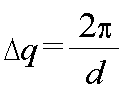
그리고, XRR의 세기는 도 3에 도시된 바와 같이 q의 값이 커짐에 따라 급격히 감쇄하는 것을 볼 수 있으며, 도 5와 같이 시료 표면의 거칠기가 있는 경우에는 XRR의 세기가 더욱 급격하게 감쇄한다. 다시 말하여, 보통 거칠기가 없을 때의 XRR의 세기 I(q)가 거칠기의 rms 값이 σ인 경우 
![]()
![]()


![]()
![]()
이에, 본 발명은 상기와 같은 문제점을 해결하기 위하여 안출한 것으로서, 그 목적은 XRR에 대한 퓨리에 변환을 수행하기 전에 XRR의 측정치에 웨이팅 펙터를 곱하여 XRR의 감쇄 효과를 보정하며, 또한 동적 스캐터링에 의한 XRR의 결과를 운동학적 스캐터링으로 가정하고 분석하는 경우에 파동벡터 q의 값을 X선의 굴절율에 의해 변하는 것을 감안하여 
이러한 목적을 달성하기 위한 본 발명에서 극초박막의 두께 측정을 위한 XRR 분석방법은 시료에서 입사된 X선의 세기에 대하여 반사된 X선의 세기의 비인 XRR은 파동벡터 q의 함수로 나타내며, 

이하, 본 발명의 실시 예는 다수개가 존재할 수 있으며, 이하에서 첨부한 도면을 참조하여 바람직한 실시 예에 대하여 상세히 설명하기로 한다. 이 기술 분야의 숙련자라면 이 실시 예를 통해 본 발명의 목적, 특징 및 이점들을 잘 이해하게 될 것이다.Hereinafter, a plurality of embodiments of the present invention may exist, and a preferred embodiment will be described in detail with reference to the accompanying drawings. Those skilled in the art will appreciate the objects, features and advantages of the present invention through this embodiment.
도 10은 본 발명에 따른 다이나믹 스캐터링에 의한 XRR의 결과를 키너메틱 스캐터링으로 가정한 퓨리에 변환을 통하여 분석하는 방법을 도시한 흐름도로서, 이에 대하여 보다 상세하게 설명하면 하기와 같다.10 is a flowchart illustrating a method of analyzing a result of XRR by dynamic scattering through Fourier transform assuming kinematic scattering, which will be described in detail below.
즉, 다이나믹 스캐터링에 의한 XRR의 결과를 키너메틱 스캐터링으로 가정한 퓨리에 변환을 통하여 분석하는 경우에는, 시료에 대하여 극초박막의 두께를 측정하기 위해서는 X선이 시료에서 입사된 X선의 세기에 대하여 반사된 X선의 세기의 비를 의미하는 XRR 기법을 통해 XRR을 측정한다(단계 101). 이때, XRR은 파동벡터 

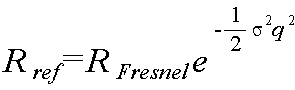
이어서, 상술한 바와 같이 측정된 XRR의 측정치(Rmea)에 웨이팅 펙터(Rref)를 수학식 1과 같이 곱하여 시료 표면의 거칠기에 따른 XRR의 감쇄를 보정한다(단계 102). Subsequently, the attenuation of XRR according to the roughness of the surface of the sample is corrected by multiplying the measured value R mea of XRR measured as described above by the weighting factor R ref as in Equation 1 (step 102).

여기서, Rmea는 XRR의 측정치이고, Rref는 XRR의 측정치(Rmea)와 동일한 형태를 갖도록 하기 위하여 임계각(critical angle), 거칠기(roughness), 최대치 파동벡터(QZ max)를 도 5 및 도 6 그리고 도 7에 도시된 계산 값들을 고려하여 얻을 수 있다. Here, R mea is a measurement of XRR, and R ref is a critical angle, roughness, and maximum wave vector Q Z max in order to have the same shape as that of XRR (R mea ). This may be obtained by considering the calculated values shown in FIGS. 6 and 7.
즉, 임계각은 검출기의 노이즈 이전 부분까지 분석이 가능한 최대 Qz 영역을 정한 다음 아래의 수학식 2를 이용하여 결정한다.That is, the critical angle is determined using the following
![]()
![]()
여기서, ρe 는 표면에 위치한 굴절율이 큰 물질의 전자 밀도이고, qc는 박막의 임계 파동벡터의 값이다. Where ρ e is the electron density of the large refractive index material and q c is the value of the critical wave vector of the thin film.
그리고, 거칠기는 수학식 3을 사용하여 실제 데이터와 비교하면서 앞서 정한 Qz,max 까지 데이터에 가장 근접하는 커브의 σ값을 선택한다.Then, the roughness is selected using the equation (3) to select the σ value of the curve that is closest to the data up to Q z, max as previously determined.

다음으로, 도 5는 XRR 커브들의 표면 거칠기에 대한 의존도를 도시한 도면으로서, 레퍼런스 커브의 임계각을 일치시키기 위하여 HfO2 기판 커브를 선택한 것을 나타낸다. 그리고, 도 6은 수학식 1의 계산과정을 통해 시료 표면의 거칠기에 따른 XRR의 감쇄를 보정한 도면으로서, 기울기의 편차가 발생하며, 이 편차는 얇은 두께 정보가 있는 high-Q 영역에서 점점 커짐을 알 수 있다. 더불어 도 7은 극초박막 두께 값의 오차를 도시한 도면으로서, 극초박막 두께 값의 오차가 도 6에 의한 기울기 편차가 커짐에 따라 점점 커짐을 알 수 있다. Next, FIG. 5 shows the dependence of the surface roughness of the XRR curves, showing that the HfO 2 substrate curve was selected to match the critical angle of the reference curve. FIG. 6 is a diagram of correcting attenuation of XRR according to roughness of a sample surface through the calculation process of
다음으로, 수학식 1과 같이 XRR의 측정치(Rmea)에 웨이팅 펙터(Rref)를 곱하여 시료 표면의 거칠기에 따른 XRR의 감쇄를 보정한 후, 파동벡터 q의 값을 X선의 굴절율에 의해 변하는 것을 감안하여 

이와 같은 패터슨(Patterson) 함수를 이용하여 전자밀도 차이가 작은 층의 두께 정보를 얻기 위한 퓨리에 변환을 수행하여 극초박막의 두께를 측정한다(단계 104). Using the Patterson function, Fourier transform is performed to obtain thickness information of a layer having a small electron density difference, and the thickness of the ultra-thin film is measured (step 104).
한편, 상기와는 달리 본 발명은, 파동벡터 q의 값을 X선의 굴절율에 의해 변하는 것을 감안하여 
한편, 도 8 및 도 9는 여러 두께(6㎚, 9㎚, 12㎚)의 HfO2 박막과 실리콘 기판 사이에 계면층이 있는 경우에 대하여 상기와 같은 본 발명에 의한 방법을 적용 시켜 분석한 도면으로서, 도 8은 XRR 데이터가 측정된 것을 도시한 것을 나타내며, 도 9는 XRR의 분석방법에 의해 그 결과를 도시한 도면이다. 8 and 9 are applied to the method according to the present invention as described above with respect to the case where the interface layer between the HfO 2 thin film of various thicknesses (6nm, 9nm, 12nm) and the silicon substrate. 8 shows that the XRR data is measured, and FIG. 9 shows the results by the XRR analysis method.
즉, 도 9를 참조하면, 여러 두께(6㎚, 9㎚, 12㎚)의 HfO2 박막과 실리콘 기판 사이에 있는 계면층의 두께를 XRR 기반을 통해 측정한 분석 결과를 살펴보면, 종래 도 4에서와는 달리 각 피크들이 잘 분리되어 나타나고 있을 뿐만 아니라 고조파(higher harmonics)에 해당하는 피크들도 뚜렷하게 나타나고 있음을 알 수 있으며, 또한 분석 결과를 TEM의 측정치와 비교해 볼 때 두 가지의 분석 결과들이 잘 일치하고 있어, 본 발명에 의한 분석 결과의 신뢰도가 매우 높은 것임을 알 수 있다.That is, referring to FIG. 9, when the thickness of the interface layer between the HfO 2 thin film having various thicknesses (6 nm, 9 nm, and 12 nm) and the silicon substrate is measured based on XRR, the analysis result of FIG. In addition, each peak is not only separated well but also the peaks corresponding to higher harmonics are clearly displayed. Also, when comparing the analysis results with the TEM measurements, the two analysis results agree well. Therefore, it can be seen that the reliability of the analysis results according to the present invention is very high.
따라서, XRR의 변화를 분석하여 고유전율 박막과 실리콘 기판 사이에 존재하는 계면층인 박막의 두께를 측정함에 있어서, XRR에 대한 퓨리에 변환을 수행하기 전에 XRR의 측정치에 웨이팅 펙터를 곱하여 XRR의 감쇄 효과를 보정하며, 또한 동적 스캐터링에 의한 XRR의 결과를 운동학적 스캐터링으로 가정하고 분석하는 경우에 파동벡터 q의 값을 X선의 굴절율에 의해 변하는 것을 감안하여 
또한, 본 발명의 사상 및 특허청구범위 내에서 권리로서 개시하고 있으므로, 본 발명은 일반적인 원리들을 이용한 임의의 변형, 이용 및/또는 개작을 포함할 수 도 있으며, 본 명세서의 설명으로부터 벗어나는 사항으로서 본 발명이 속하는 업계에서 공지 또는 관습적 실시의 범위에 해당하고 또한 첨부된 특허청구범위의 제한 범위 내에 포함되는 모든 사항은 포함한다.Furthermore, since the invention is disclosed as a right within the spirit and claims of the invention, the invention may include any modification, use, and / or adaptation using general principles, and as a matter departs from the description herein. All matters falling within the scope of known or customary practice in the art to which the invention pertains and fall within the scope of the appended claims are included.
이상, 상기에서 설명한 바와 같이, 본 발명은 XRR의 변화를 분석하여 고유전율 박막과 실리콘 기판 사이에 존재하는 계면층인 박막의 두께를 측정함에 있어서, XRR에 대한 퓨리에 변환을 수행하기 전에 XRR의 측정치에 웨이팅 펙터를 곱하여 XRR의 감쇄 효과를 보정하며, 또한 동적 스캐터링에 의한 XRR의 결과를 운동학적 스캐터링으로 가정하고 분석하는 경우에 파동벡터 q의 값을 X선의 굴절율에 의해 변하는 것을 감안하여 
상기와 같이 X선 굴절율의 차이가 큰 층 사이에 있는 1㎚의 계면층(X선 굴절율의 차이가 작은)의 두께를 정확하게 측정할 수 있고, 특히 고유전율 산화막과 실리콘 기판 사이의 계면층의 두께를 비파괴적으로 측정할 수 있게 됨으로써 반도체 공정에서 인 라인(in-line) 분석 장비로 개발을 기대할 수 있다. As described above, the thickness of the 1 nm interface layer (small difference in X-ray refractive index) between the layers having a large difference in X-ray refractive index can be accurately measured, and in particular, the thickness of the interface layer between the high dielectric constant oxide film and the silicon substrate. By being able to measure nondestructively, it can be expected to be developed as an in-line analysis equipment in the semiconductor process.
또한, 본 발명은 반도체의 고집적화에 따라 산화막의 두께가 감소함에 의한 성능저하를 막기 위한 대안으로 개발중인 고유전율 박막의 제조과정에서 불가피하게 생성되는 계면층의 두께를 분석하기 위한 분석방법으로 활용할 수 있는 효과가 있다. In addition, the present invention can be utilized as an analytical method for analyzing the thickness of the interface layer inevitably generated in the manufacturing process of the high-k dielectric thin film under development as an alternative to prevent performance degradation due to the decrease in the thickness of the oxide film in accordance with the high integration of the semiconductor. It has an effect.
Claims (6)


Priority Applications (1)
| Application Number | Priority Date | Filing Date | Title |
|---|---|---|---|
| KR1020050065105A KR100721810B1 (en) | 2005-07-19 | 2005-07-19 | Jr analysis method for ultra-thin film thickness measurement |
Applications Claiming Priority (1)
| Application Number | Priority Date | Filing Date | Title |
|---|---|---|---|
| KR1020050065105A KR100721810B1 (en) | 2005-07-19 | 2005-07-19 | Jr analysis method for ultra-thin film thickness measurement |
Publications (2)
| Publication Number | Publication Date |
|---|---|
| KR20070010487A KR20070010487A (en) | 2007-01-24 |
| KR100721810B1 true KR100721810B1 (en) | 2007-05-25 |
Family
ID=38011703
Family Applications (1)
| Application Number | Title | Priority Date | Filing Date |
|---|---|---|---|
| KR1020050065105A KR100721810B1 (en) | 2005-07-19 | 2005-07-19 | Jr analysis method for ultra-thin film thickness measurement |
Country Status (1)
| Country | Link |
|---|---|
| KR (1) | KR100721810B1 (en) |
Cited By (2)
| Publication number | Priority date | Publication date | Assignee | Title |
|---|---|---|---|---|
| WO2014065473A1 (en) * | 2012-10-26 | 2014-05-01 | 나노씨엠에스(주) | Method and device for measuring thickness of thin film layer using x-rays |
| US9417055B2 (en) | 2014-08-28 | 2016-08-16 | Samsung Electronics Co., Ltd. | Apparatus for measuring thickness of thin film, system including the apparatus, and method for measuring thickness of thin film |
Citations (3)
| Publication number | Priority date | Publication date | Assignee | Title |
|---|---|---|---|---|
| JPH021A (en) * | 1989-05-09 | 1990-01-05 | Seiko Epson Corp | Color filter |
| JPH03228344A (en) * | 1990-02-01 | 1991-10-09 | Fujitsu Ltd | Evaluation of composite film |
| KR20040072780A (en) * | 2003-02-11 | 2004-08-19 | 삼성전자주식회사 | Method for measuring a thickness of a thin layer |
-
2005
- 2005-07-19 KR KR1020050065105A patent/KR100721810B1/en not_active IP Right Cessation
Patent Citations (3)
| Publication number | Priority date | Publication date | Assignee | Title |
|---|---|---|---|---|
| JPH021A (en) * | 1989-05-09 | 1990-01-05 | Seiko Epson Corp | Color filter |
| JPH03228344A (en) * | 1990-02-01 | 1991-10-09 | Fujitsu Ltd | Evaluation of composite film |
| KR20040072780A (en) * | 2003-02-11 | 2004-08-19 | 삼성전자주식회사 | Method for measuring a thickness of a thin layer |
Non-Patent Citations (1)
| Title |
|---|
| 논문 2001년 |
Cited By (2)
| Publication number | Priority date | Publication date | Assignee | Title |
|---|---|---|---|---|
| WO2014065473A1 (en) * | 2012-10-26 | 2014-05-01 | 나노씨엠에스(주) | Method and device for measuring thickness of thin film layer using x-rays |
| US9417055B2 (en) | 2014-08-28 | 2016-08-16 | Samsung Electronics Co., Ltd. | Apparatus for measuring thickness of thin film, system including the apparatus, and method for measuring thickness of thin film |
Also Published As
| Publication number | Publication date |
|---|---|
| KR20070010487A (en) | 2007-01-24 |
Similar Documents
| Publication | Publication Date | Title |
|---|---|---|
| US6507634B1 (en) | System and method for X-ray reflectometry measurement of low density films | |
| US7321426B1 (en) | Optical metrology on patterned samples | |
| US11906451B2 (en) | Method and system for non-destructive metrology of thin layers | |
| US8119991B2 (en) | Method and apparatus for accurate calibration of VUV reflectometer | |
| US7466428B2 (en) | Method of measuring thickness of thin layer in semiconductor device and apparatus for performing method | |
| US6222199B1 (en) | Ultrathin layer measurement having a controlled ambient of light path | |
| US6825938B2 (en) | Film thickness measuring method and step measuring method | |
| TWI761788B (en) | Device and substrate assisted x-ray leakage method for ultrathin film thickness measurement | |
| KR100721810B1 (en) | Jr analysis method for ultra-thin film thickness measurement | |
| US20180180561A1 (en) | Model Independent Grazing Incidence X-Ray Reflectivity | |
| Hilfiker et al. | Data analysis | |
| KR20040072780A (en) | Method for measuring a thickness of a thin layer | |
| JP3781245B2 (en) | Manufacturing method of semiconductor device | |
| US5717490A (en) | Method for identifying order skipping in spectroreflective film measurement equipment | |
| WO2007009078A1 (en) | Methods and systems for characterizing semiconductor materials | |
| US7570353B2 (en) | Fabrication and test methods and systems | |
| Paulson et al. | Accurate determination of optical constants of textured SnO2 using low incidence angle spectroscopic ellipsometry | |
| US7580138B2 (en) | Methods and systems for characterizing semiconductor materials | |
| TWI741526B (en) | Method and system for monitoring deposition process | |
| JP3883267B2 (en) | Structure analysis method of metal multilayer film by X-ray reflectivity measurement and fluorescent X-ray measurement, and standard sample and apparatus used therefor | |
| KR100969213B1 (en) | Membrane Structure Analysis Method and Apparatus | |
| JP3339243B2 (en) | X-ray reflectance analysis method and apparatus | |
| Deslattes et al. | Analysis of thin-layer structures by X-ray reflectometry | |
| US20240201077A1 (en) | Phase-Resolved Optical Metrology for Substrates | |
| WO2020003675A1 (en) | Total reflection x-ray fluorescence analysis device and measuring method |
Legal Events
| Date | Code | Title | Description |
|---|---|---|---|
| A201 | Request for examination | ||
| PA0109 | Patent application |
Patent event code: PA01091R01D Comment text: Patent Application Patent event date: 20050719 |
|
| PA0201 | Request for examination | ||
| E902 | Notification of reason for refusal | ||
| PE0902 | Notice of grounds for rejection |
Comment text: Notification of reason for refusal Patent event date: 20060825 Patent event code: PE09021S01D |
|
| PG1501 | Laying open of application | ||
| E701 | Decision to grant or registration of patent right | ||
| PE0701 | Decision of registration |
Patent event code: PE07011S01D Comment text: Decision to Grant Registration Patent event date: 20070226 |
|
| GRNT | Written decision to grant | ||
| PR0701 | Registration of establishment |
Comment text: Registration of Establishment Patent event date: 20070518 Patent event code: PR07011E01D |
|
| PR1002 | Payment of registration fee |
Payment date: 20070521 End annual number: 3 Start annual number: 1 |
|
| PG1601 | Publication of registration | ||
| PR1001 | Payment of annual fee |
Payment date: 20100430 Start annual number: 4 End annual number: 4 |
|
| PR1001 | Payment of annual fee |
Payment date: 20110411 Start annual number: 5 End annual number: 5 |
|
| FPAY | Annual fee payment |
Payment date: 20120404 Year of fee payment: 6 |
|
| PR1001 | Payment of annual fee |
Payment date: 20120404 Start annual number: 6 End annual number: 6 |
|
| LAPS | Lapse due to unpaid annual fee | ||
| PC1903 | Unpaid annual fee |