KR100685164B1 - High efficiency slot fed microstrip antenna having an improved stub - Google Patents
High efficiency slot fed microstrip antenna having an improved stub Download PDFInfo
- Publication number
- KR100685164B1 KR100685164B1 KR1020057018424A KR20057018424A KR100685164B1 KR 100685164 B1 KR100685164 B1 KR 100685164B1 KR 1020057018424 A KR1020057018424 A KR 1020057018424A KR 20057018424 A KR20057018424 A KR 20057018424A KR 100685164 B1 KR100685164 B1 KR 100685164B1
- Authority
- KR
- South Korea
- Prior art keywords
- dielectric
- region
- slot
- antenna
- relative
- Prior art date
Links
Images


Classifications
-
- H—ELECTRICITY
- H01—ELECTRIC ELEMENTS
- H01Q—ANTENNAS, i.e. RADIO AERIALS
- H01Q13/00—Waveguide horns or mouths; Slot antennas; Leaky-waveguide antennas; Equivalent structures causing radiation along the transmission path of a guided wave
- H01Q13/08—Radiating ends of two-conductor microwave transmission lines, e.g. of coaxial lines, of microstrip lines
- H01Q13/085—Slot-line radiating ends
-
- H—ELECTRICITY
- H01—ELECTRIC ELEMENTS
- H01Q—ANTENNAS, i.e. RADIO AERIALS
- H01Q1/00—Details of, or arrangements associated with, antennas
- H01Q1/36—Structural form of radiating elements, e.g. cone, spiral, umbrella; Particular materials used therewith
- H01Q1/38—Structural form of radiating elements, e.g. cone, spiral, umbrella; Particular materials used therewith formed by a conductive layer on an insulating support
-
- H—ELECTRICITY
- H01—ELECTRIC ELEMENTS
- H01Q—ANTENNAS, i.e. RADIO AERIALS
- H01Q1/00—Details of, or arrangements associated with, antennas
- H01Q1/48—Earthing means; Earth screens; Counterpoises
-
- H—ELECTRICITY
- H01—ELECTRIC ELEMENTS
- H01Q—ANTENNAS, i.e. RADIO AERIALS
- H01Q13/00—Waveguide horns or mouths; Slot antennas; Leaky-waveguide antennas; Equivalent structures causing radiation along the transmission path of a guided wave
- H01Q13/10—Resonant slot antennas
- H01Q13/106—Microstrip slot antennas
-
- H—ELECTRICITY
- H01—ELECTRIC ELEMENTS
- H01Q—ANTENNAS, i.e. RADIO AERIALS
- H01Q9/00—Electrically-short antennas having dimensions not more than twice the operating wavelength and consisting of conductive active radiating elements
- H01Q9/04—Resonant antennas
- H01Q9/0407—Substantially flat resonant element parallel to ground plane, e.g. patch antenna
-
- H—ELECTRICITY
- H01—ELECTRIC ELEMENTS
- H01Q—ANTENNAS, i.e. RADIO AERIALS
- H01Q9/00—Electrically-short antennas having dimensions not more than twice the operating wavelength and consisting of conductive active radiating elements
- H01Q9/04—Resonant antennas
- H01Q9/0485—Dielectric resonator antennas
Abstract
개선된 스터브(118)를 구비한 슬롯 급전 마이크로스트립 안테나(100)는 급전선(117) 및 슬롯(106) 사이에 전자기 에너지의 보다 효율적인 커플링을 통해 개선된 효율을 제공한다. 상기 급전선(117) 및 접지면(108) 사이에 배치된 유전층(105)은 제1 상대 유전율을 갖는 제1 영역(112) 및 제2 상대 유전율을 갖는 적어도 하나의 제2 영역(113)을 포함한다. 제2 상대 유전율은 제1 상대 유전율에 비해 높다. 스터브(118)가 높은 유전율을 갖는 제2 영역(113) 상에 배치된다. 유전층(105)은 자성 입자를 포함할 수 있고, 스터브(118) 밑에 배치되는 것이 바람직하다.Slot fed microstrip antenna 100 with improved stub 118 provides improved efficiency through more efficient coupling of electromagnetic energy between feedline 117 and slot 106. The dielectric layer 105 disposed between the feed line 117 and the ground plane 108 includes a first region 112 having a first relative permittivity and at least one second region 113 having a second relative permittivity. do. The second relative permittivity is higher than the first relative permittivity. The stub 118 is disposed on the second region 113 having a high dielectric constant. The dielectric layer 105 may include magnetic particles and is preferably disposed under the stub 118.
안테나, 마이크로스트립, 스터브, 유전율, 투자율, 메타-물질 Antennas, microstrips, stubs, permittivity, permeability, meta-materials
Description
본 발명은 개선된 스터브를 구비하는 고효율 슬롯 급전 마이크로스트립 안테나에 관한 것이다.The present invention is directed to a high efficiency slot fed microstrip antenna with improved stubs.
통상적으로, 무선주파수 회로, 전송선 및 안테나 구성요소는 특별히 설계된 기판 상에 제조된다. 일반적으로, 종래의 회로 기판은 유전율을 포함한 기판의 물리적 특성들을 균일하게 하는 캐스팅 및 스프레이 코팅과 같은 방법으로 형성된다.Typically, radiofrequency circuits, transmission lines and antenna components are fabricated on specially designed substrates. In general, conventional circuit boards are formed by methods such as casting and spray coating that uniform the physical properties of the substrate, including the dielectric constant.
무선주파수 회로를 목적으로 하는 경우, 임피던스 특성을 신중하게 제어하여 유지하는 것이 중요하다. 무선주파수 회로의 서로 다른 부분들의 임피던스가 정합되지 않으면, 신호가 반사될 수 있고, 전력이 비효율적으로 전달될 수 있다. 또한, 이러한 무선주파수 회로에서 전송선 및 방사체의 전기적 길이는 중요한 설계 인자가 될 수 있다.For the purpose of radiofrequency circuits, it is important to carefully control and maintain the impedance characteristics. If the impedances of the different parts of the radiofrequency circuit are not matched, the signal may be reflected and power may be delivered inefficiently. In addition, the electrical length of the transmission line and the radiator may be an important design factor in such radio frequency circuit.
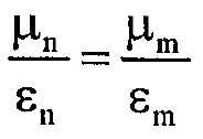
회로 성능에 영향을 미치는 2개의 중요한 인자는 유전체 기판 물질의 유전율(종종 상대 유전율 ![]()
![]()
![]()
![]()
무선주파수 회로에서 사용되는 인쇄된 전송선, 수동 회로 및 방사 부품은 전형적으로 3가지 방식 중에서 어느 한 방식으로 구성된다. 마이크로스트립으로 알려진 첫 번째 구성 방식은 기판 상에 신호선을 배치하고, 통상적으로 접지면으로 불리는 제2 도전층을 제공한다. 매립형 마이크로스트립으로 알려진 두 번째 구성 방식은 신호선이 유전체 기판 물질로 덮이는 것을 제외하면 첫 번째 방식과 유사하다. 스트립선으로 알려진 세 번째 구성 방식은 신호선이 2개의 전기적으로 도전된(접지) 면들 사이에 샌드위치 형식으로 삽입된다.Printed transmission lines, passive circuits and radiating components used in radiofrequency circuits are typically constructed in one of three ways. The first configuration, known as microstrip, arranges signal lines on a substrate and provides a second conductive layer, commonly referred to as ground plane. The second configuration, known as buried microstrip, is similar to the first, except that the signal lines are covered with a dielectric substrate material. A third configuration, known as strip line, is where the signal line is sandwiched between two electrically conductive (grounded) faces.
일반적으로, 스트립선 또는 마이크로스트립선과 같은 평판 전송선의 특성 임피던스는 대략적으로 ![]()
![]()
![]()
![]()
![]()
![]()
![]()
![]()
![]()
![]()
종래의 무선주파수(RF) 설계에서, 기판 물질은 단일 유전율 및 단일 상대 투자율을 갖는 것으로 선택되며, 이때, 상대 투자율 값은 약 1이다. 일단 기판 물질이 선택되면, 선 특성 임피던스 값은 선 및 슬롯의 형상을 제어함으로써 그리고 선 및 슬롯의 특성을 커플링함으로써 배타적으로 설정된다.In conventional radiofrequency (RF) designs, the substrate material is selected to have a single permittivity and a single relative permeability, with a relative permeability value of about 1. Once the substrate material is selected, the line characteristic impedance values are set exclusively by controlling the shape of the lines and slots and by coupling the properties of the lines and slots.
전형적으로 무선주파수(RF) 회로는 세라믹 기판과 같은 전기적으로 절연인 기판의 표면상에 복수의 능동 및 수동 소자들을 실장하고 서로 연결한 하이브리드 회로로 구현된다. 일반적으로 여러 소자들은 구리, 금 또는 탄탈륨과 같은 인쇄된 금속 도전체에 의해 상호 연결되는데, 금속 도전체는 일반적으로 해당 주파수 범위에서 전송선(예를 들면, 스트립선, 마이크로스트립선 또는 이중선)으로서 작용한다.Typically, radio frequency (RF) circuits are implemented as hybrid circuits in which a plurality of active and passive elements are mounted and interconnected on the surface of an electrically insulated substrate, such as a ceramic substrate. In general, several devices are interconnected by printed metal conductors, such as copper, gold or tantalum, which typically act as transmission lines (eg, strip lines, microstrip lines or double lines) in the frequency range of interest. do.
전송선, 수동 RF 소자 또는 방사 부품을 위해 선택된 기판 물질의 유전율은 해당 구조에 대해 주어진 주파수에서 RF 에너지의 물리적 파장을 결정한다. 마이크로전자 RF 회로를 설계할 때 당면하는 한 가지 문제점은 기판 상에 형성되는 여러 수동 소자, 방사 부품 및 전송선 회로 모두에 대해 적합한 유전체 기판을 타당하게 선택해야 한다는 점이다.The dielectric constant of the substrate material selected for the transmission line, passive RF device, or radiating component determines the physical wavelength of the RF energy at a given frequency for that structure. One problem faced in designing microelectronic RF circuits is the need to make reasonable choices of suitable dielectric substrates for all of the passive components, radiating components, and transmission line circuits formed on the substrate.
특히, 임의의 회로 구성요소들의 기하학적 형상은 이러한 구성요소들에 대해 요구되는 고유의 전기적 특성 및 임피던스 특성에 기인하여 물리적으로 커지거나 또는 작아질 수 있다. 예를 들면, 많은 회로 구성요소 또는 동조된 회로는 파장의 1/4인 전기적 길이를 가질 필요가 있다. 마찬가지로, 예외적으로 높거나 낮은 특성 임피던스 값을 요구하는 선 폭은 많은 경우에 있어서 주어진 기판에 대해 실질적으로 구현하기에는 지나치게 좁거나 또는 지나치게 넓을 수 있다. 마이크로스트립선 또는 스트립선의 물리적인 크기가 유전체 물질의 유전율에 반비례하기 때문에, 전송선 또는 방사 부품의 크기는 기판 물질의 선택에 의해 크게 영향을 받을 수 있다.In particular, the geometry of any circuit components may be physically larger or smaller due to the inherent electrical and impedance characteristics required for these components. For example, many circuit components or tuned circuits need to have an electrical length that is one quarter of the wavelength. Likewise, line widths that require exceptionally high or low characteristic impedance values can in many cases be too narrow or too wide to be practical for a given substrate. Since the physical size of the microstrip line or strip line is inversely proportional to the dielectric constant of the dielectric material, the size of the transmission line or radiating component can be greatly influenced by the choice of substrate material.
더욱이, 일부 부품에 대한 최적의 기판 물질 설계 선택은 안테나 부품과 같은 다른 부품에 대한 최적의 기판 물질과 일치하지 않을 수 있다. 또한, 하나의 회로 부품에 대한 일부 설계 목적이 서로 일치하지 않을 수 있다. 예를 들면, 안테나 부품의 크기를 축소하는 것이 바람직할 수 있다. 이것은 50 내지 100과 같은 높은 유전율 값을 갖는 기판 물질을 선택함으로써 달성될 수 있다. 하지만, 일반적으로 높은 유전율을 갖는 유전체의 사용은 안테나의 방사 효율을 상당히 떨어뜨리는 결과를 가져온다. Moreover, the optimal substrate material design choice for some components may not match the optimal substrate material for other components, such as antenna components. In addition, some design goals for one circuit component may be inconsistent with each other. For example, it may be desirable to reduce the size of the antenna component. This can be accomplished by selecting a substrate material having a high dielectric constant value, such as 50-100. In general, however, the use of a dielectric having a high permittivity results in a significant decrease in the radiation efficiency of the antenna.
안테나 부품은 종종 마이크로스트립 슬롯 안테나와 같은 구조를 갖는다. 마이크로스트립 슬롯 안테나는 일반적으로 좁은 공간을 요구하고, 다른 안테나 종류에 비해 제조가 간단하고 제조비용이 적게 들기 때문에 유용한 안테나이다. 또한, 중요한 사항으로서, 마이크로스트립 슬롯 안테나는 인쇄-회로 기술과 호환성이 높다는 점이다.Antenna components often have the same structure as microstrip slot antennas. Microstrip slot antennas are generally useful antennas because they require less space and are simpler to manufacture and less expensive to manufacture than other antenna types. Also important is the microstrip slot antenna being highly compatible with the printed-circuit technology.
고효율의 마이크로스트립 슬롯 안테나 구성시 한 가지 인자는 전력 손실을 최소화하는 것이고, 이것은 유전 손실을 포함한 여러 인자들에 의해 야기될 수 있다. 일반적으로 유전 손실은 경계 전하의 불완전한 활동에 기인하며, 유전체 물질이 시변 전자기장에 놓일 때마다 존재하게 된다. 종종 손실 정접(loss tangent)으로 불리는 유전 손실은 유전체 매개물의 도전성에 정비례한다. 일반적으로 유전 손실은 동작 주파수가 증가함에 따라 함께 증가한다.One factor in the construction of high efficiency microstrip slot antennas is to minimize power loss, which can be caused by several factors including dielectric loss. In general, dielectric loss is due to the incomplete activity of the boundary charge, which is present whenever the dielectric material is placed in a time-varying electromagnetic field. Dielectric loss, often referred to as loss tangent, is directly proportional to the conductivity of the dielectric medium. In general, dielectric losses increase with increasing operating frequency.
특정한 마이크로스트립 슬롯 안테나에 대한 유전 손실 정도는 방사체 안테나 부품(예를 들면, 슬롯) 및 급전선 사이의 유전 공간의 유전율에 의해 주로 결정된다. 자유 공간에서는, 즉 대부분의 경우 공기 중에서는 상대 유전율 및 상태 투자율이 거의 1에 가깝다.The degree of dielectric loss for a particular microstrip slot antenna is mainly determined by the permittivity of the dielectric space between the radiator antenna component (eg, slot) and the feed line. In free space, ie in most cases relative permittivity and state permeability in air are close to one.
양호한 유전체 물질은 낮은 유전 손실을 보이기 때문에, 상대 유전율이 1에 가까운 유전체 물질은 해당 동작 주파수에서 "양호"한 유전체 물질로 간주된다. 상대 유전율이 실질적으로 주변 물질과 같은 유전체 물질이 사용될 때, 임피던스 부정합에 기인하는 유전 손실은 효율적으로 제거될 수 있다. 따라서 마이크로스트립 슬롯 안테나 시스템에서 고효율을 유지하는 한 가지 방법은 방사체 안테나 슬롯 및 슬롯을 활성화시키는 마이크로스트립 급전선 사이의 유전 공간 내의 낮은 상대 유전율을 갖는 물질을 사용하는 것과 관련이 있다.Since good dielectric materials exhibit low dielectric losses, dielectric materials with relative permittivity close to 1 are considered to be "good" dielectric materials at their operating frequencies. When a dielectric material whose relative permittivity is substantially the same as the surrounding material is used, the dielectric loss due to impedance mismatch can be efficiently eliminated. Thus, one method of maintaining high efficiency in a microstrip slot antenna system involves the use of materials with low relative permittivity in the dielectric space between the radiator antenna slot and the microstrip feedline activating the slots.
또한, 낮은 유전율을 갖는 물질의 사용은 넓은 전송선을 사용할 수 있게 하는데, 이때 넓은 전송선을 사용할 경우 도전 손실을 줄이고, 또한 마이크로스트립 슬롯 안테나의 방사 효율을 향상시킬 수 있다. 하지만, 낮은 유전율을 갖는 유전체 물질을 사용할 경우, 높은 유전율을 갖는 기판 상에 제조되는 슬롯 안테나에 비해 낮은 유전율을 갖는 기판 상에 제조되는 슬롯 안테나의 크기가 커지는 단점이 있다.In addition, the use of a material having a low permittivity allows the use of a wide transmission line, which can reduce the conduction loss and improve the radiation efficiency of the microstrip slot antenna. However, when using a dielectric material having a low dielectric constant, there is a disadvantage in that the size of a slot antenna manufactured on a substrate having a low dielectric constant is larger than that of a slot antenna manufactured on a substrate having a high dielectric constant.
마이크로스트립 슬롯 안테나의 효율은 단일의 균일한 유전율을 갖는 급전선용의 특정한 유전체 물질의 선택을 통해 절충된다. 낮은 유전율은 넓은 급전선을 허용하는데, 이때, 넓은 급전선은 보다 낮은 저항 손실을 제공할 수 있고, 유전체로부터 유도된 선 손실을 최소화하고, 슬롯 방사 효율을 최소화시킨다. 하지만, 유전체 물질이 슬롯 및 급전선 사이의 접합 영역에 놓일 경우, 이용 가능한 유전체 물질은 슬롯에 대한 열악한 커플링 특성에 기인하여 안테나 방사 효율을 떨어뜨리게 된다.The efficiency of the microstrip slot antenna is compromised through the selection of specific dielectric materials for feeders with a single uniform dielectric constant. Low permittivity allows for wide feed lines, which can provide lower resistive losses, minimize line losses induced from the dielectric, and minimize slot radiation efficiency. However, if the dielectric material is placed in the junction region between the slot and the feed line, the available dielectric material will degrade the antenna radiation efficiency due to poor coupling characteristics for the slot.
통상적으로, 동조 스터브가 마이크로스트립 슬롯 안테나에서 과도한 유도저항을 조정하는데 사용된다. 하지만, 일반적으로 스터브의 임피던스 대역폭은 방사체의 대역폭과 슬롯의 대역폭보다는 적다. 따라서 종래의 스터브가 안테나 회로의 과도한 유도저항을 조정하는데 사용될지라도, 일반적으로 스터브의 적은 임피던스 대역폭은 전체 안테나 회로의 성능을 제한하게 된다.Typically, tuning stubs are used to adjust excessive inductive resistance in microstrip slot antennas. In general, however, the impedance bandwidth of the stub is less than the bandwidth of the radiator and the slot. Thus, although conventional stubs are used to adjust the excessive inductive resistance of the antenna circuit, generally the low impedance bandwidth of the stub will limit the performance of the entire antenna circuit.
마이크로스트립 안테나의 성능은 급전 스터브의 성능을 개선함으로써 최적화될 수 있다. 통상적으로, 급전 스터브는 슬롯 급전 안테나의 과도한 리액턴스를 조정하는데 사용되지만, 통상적인 균일한 유전체 기판에 의해 부과되는 한계 때문에 설게 호환성에 제한을 받는다. 일반적으로, 통상적인 유전체 기판은 양호한 전송선 특성을 획득하기 위해 선택된다. 본 발명을 사용하여, 스터브 밑에 있을 뿐만 아니라 슬롯에 걸쳐있는 유전체 기판 영역은 양호한 전송선 특성을 위해 요구되는 유전체 기판 특성과 별도로 최적화될 수 있다.The performance of the microstrip antenna can be optimized by improving the performance of the feed stub. Typically, feed stubs are used to adjust for excessive reactance of slot feed antennas, but are limited in compatibility due to the limitations imposed by conventional uniform dielectric substrates. In general, conventional dielectric substrates are selected to obtain good transmission line characteristics. Using the present invention, the area of the dielectric substrate that is under the stub as well as across the slots can be optimized separately from the dielectric substrate properties required for good transmission line characteristics.
또한, 스터브 임피던스 대역폭은 높은 유전율 물질 상에 급전 스터브를 배치함으로써 개선될 수 있다. 높은 유전율을 갖는 영역추가적인 효율 향상을 위해 그 내부에 선택사항인 자성 입자를 포함하는 것이 바람직하다. 스터브 밑에 있는 유전체 영역 내에 자성 입자를 포함함으로써, 급전선과 슬롯 사이에 배치된 유전체 접합 영역의 진성 임피던스는 스터브 밑에 있는 유전체 물질로 정합될 수 있다. 이들 영역을 임피던스 정합시키면 신호 왜곡량과 불연속으로 인해 야기되는 링잉을 줄일 수 있다.In addition, the stub impedance bandwidth can be improved by placing feed stubs on high dielectric constant materials. High dielectric constant region It is desirable to include optional magnetic particles therein for further efficiency improvement. By including magnetic particles in the dielectric region under the stub, the intrinsic impedance of the dielectric junction region disposed between the feed line and the slot can be matched with the dielectric material under the stub. Impedance matching these areas can reduce ringing caused by signal distortion and discontinuities.
슬롯 급전 마이크로스트립 안테나는 적어도 하나의 슬롯을 구비한 전기적으로 도전성인 접지면을 포함한다. 급전선은 슬롯으로 또는 슬롯으로부터 신호 에너지를 전달하고, 급전선은 슬롯을 지나 연장된 스터브 영역을 포함한다. 제1 유전층이 급전선과 접지면 사이에 배치되고, 제1 유전층은 제1 영역에 대한 제1 상대 유전율을 포함하는 제1 유전체 특성 집합, 및 적어도 하나의 제2 영역에 대한 제2 상대 유전율을 포함하는 제2 유전체 특성 집합을 포함한다. 제2 유전체 특성 집합은 제1 상대 유전율에 비해 높은 상대 유전율을 제공한다. 스터브는 제2 영역 상에 배치된다.Slot fed microstrip antennas include an electrically conductive ground plane having at least one slot. The feeder line carries signal energy to or from the slots and the feeder line includes a stub region extending beyond the slot. A first dielectric layer is disposed between the feed line and the ground plane, the first dielectric layer including a first set of dielectric properties including a first relative permittivity for the first region, and a second relative permittivity for the at least one second region A second set of dielectric characteristics. The second set of dielectric properties provides a higher relative permittivity relative to the first relative permittivity. The stub is disposed on the second area.
제1 유전층은 자성 입자를 포함하는 것이 바람직하다. 자성 입자의 적어도 일부는 스터브 밑에 있는 제2 영역 내에 배치된다. 제2 영역은 적어도 1.1의 상대 투자율을 제공할 수 있다.The first dielectric layer preferably comprises magnetic particles. At least a portion of the magnetic particles are disposed in the second region below the stub. The second region may provide a relative permeability of at least 1.1.
급전선과 슬롯 사이에 배치된 유전체 접합 영역의 진성 임피던스는 스터브 밑에 있는 제1 영역에 임피던스 정합된다. 이것은 링잉 및 신호 왜곡을 감소시킨다. 또한, 유전체 접합 영역의 진성 임피던스는 안테나 주변 환경의 진성 임피던스에 임피던스 정합될 수 있다. 본 명세서 내에 사용되는 바와 같이, "진성 임피던스 정합"이라는 용어는 인터페이스를 포함하는 영역들의 각각의 실제 투자율 값이 주어지는 진성 임피던스 정합에 비해 개선된 임피던스 정합을 나타내지만, 개별 영역 각각에 대해 상대 투자율은 1이라고 가정한다. 전술한 바와 같이, 본 발명 이전에는, 기판은 단일 상대 유전율에 따른 선택을 제공하였을지라도, 이용할 수 있는 기판의 상대 투자율은 필연적으로 거의 1에 가깝다.The intrinsic impedance of the dielectric junction region disposed between the feed line and the slot is impedance matched to the first region under the stub. This reduces ringing and signal distortion. In addition, the intrinsic impedance of the dielectric junction region can be impedance matched to the intrinsic impedance of the environment around the antenna. As used herein, the term "intrinsic impedance match" refers to an improved impedance match over an intrinsic impedance match given the actual permeability value of each of the regions comprising the interface, but the relative permeability for each individual region is Assume 1 As mentioned above, prior to the present invention, although the substrate provided a choice according to a single relative permittivity, the relative permeability of the available substrates is inevitably close to one.
제1 유전층은 세라믹 물질을 포함할 수 있고, 세라믹 물질은 복수의 보이드를 구비하며, 보이드의 적어도 일부는 자성 입자로 채워진다. 자성 입자는 메타-물질을 포함할 수 있다. 안테나는 적어도 하나의 패치 방사체 및 제2 유전층을 포함하는 패치 안테나일 수 있고, 제2 유전층은 접지면과 패치 방사체 사이에 배치된다. 제2 유전층은 제3 상대 유전율을 포함하는 제3 유전체 특성 집합을 제공하는 제3 영역, 및 제4 유전체 특성 집합을 포함하는 적어도 하나의 제4 영역을 포함할 수 있다. 제4 상대 유전율은 제3 상대 유전율에 비해 높고, 패치 방사체는 제4 영역 상에 배치된다. 제4 영역은 자성 입자를 포함할 수 있고, 적어도 1.1 이상의 상대 투자율을 제공할 수 있다.The first dielectric layer may comprise a ceramic material, the ceramic material having a plurality of voids, at least a portion of the voids being filled with magnetic particles. Magnetic particles may include meta-materials. The antenna may be a patch antenna comprising at least one patch emitter and a second dielectric layer, wherein the second dielectric layer is disposed between the ground plane and the patch emitter. The second dielectric layer may include a third region that provides a third set of dielectric characteristics including a third relative dielectric constant, and at least one fourth region that includes a fourth set of dielectric characteristics. The fourth relative permittivity is higher than the third relative permittivity, and the patch emitter is disposed on the fourth region. The fourth region may comprise magnetic particles and may provide a relative permeability of at least 1.1 or greater.
본 발명은 안테나에 의해 제공되는 여러 가지 매질 인터페이스를 임피던스 정합하는데 사용될 수 있다. 예를 들면, 패치 방사체 밑에 있는 제4 영역의 진성 임피던스는 안테나 주변 환경의 진성 임피던스를 정합할 수 있다. 급전선과 슬롯 사이에 배치된 유전체 접합 영역의 진성 임피던스는 제4 영역 및/또는 스터브 아래에 있는 제2 영역의 진성 임피던스를 정합할 수 있다.The present invention can be used to impedance match various media interfaces provided by an antenna. For example, the intrinsic impedance of the fourth region underneath the patch radiator may match the intrinsic impedance of the environment around the antenna. The intrinsic impedance of the dielectric junction region disposed between the feedline and the slot may match the intrinsic impedance of the fourth region and / or the second region under the stub.
안테나는 제1 및 제2 패치 방사체와 같은 다중 패치를 포함할 수 있고, 제1 및 제2 패치 방사체는 제3 유전층에 의해 분리된다. 제3 유전층은 전술한 바와 같이 제1 및 제2 유전층에 적용되는 원리에 따라 구성될 수 있다.The antenna may comprise multiple patches, such as first and second patch emitters, wherein the first and second patch emitters are separated by a third dielectric layer. The third dielectric layer may be constructed according to the principles applied to the first and second dielectric layers as described above.
도 1은 본 발명의 실시예에 따른 고유전체 영역―여기서 스터브가 고유전체 영역 상에 배치됨― 및 저유전체 영역을 포함하는 유전체 상에 형성되는 슬롯 급전 마이크로스트립 안테나의 측면도이다.1 is a side view of a slot fed microstrip antenna formed on a dielectric comprising a high dielectric region, wherein a stub is disposed on the high dielectric region and a low dielectric region in accordance with an embodiment of the present invention.
도 2는 도 1에 도시된 마이크로스트립 안테나의 측면도로서, 스터브 밑에 있는 유전체 영역 내에 자성 입자를 추가하는 것을 나타내는 도면이다. FIG. 2 is a side view of the microstrip antenna shown in FIG. 1 illustrating the addition of magnetic particles into the dielectric region underneath the stub.
도 3은 본 발명의 다른 실시예에 따른 제1 유전체 영역―여기서, 제1 유전체 영역은 접지면과 패치 사이에 배치된 자성 입자를 포함함― 및 제2 유전체 영역―여기서, 제2 유전체 영역은 자성 입자를 포함하고 스터브 밑에 있는 고유전체 영역을 포함하고, 접지면과 급전선 사이에 배치됨―을 포함하는 슬롯 급전 마이크로스트립 패치 안테나의 측면도이다.3 shows a first dielectric region in accordance with another embodiment of the present invention, where the first dielectric region includes magnetic particles disposed between the ground plane and the patch, and the second dielectric region, wherein the second dielectric region is A side view of a slot fed microstrip patch antenna comprising magnetic particles and comprising a high dielectric region underneath the stub and disposed between the ground plane and the feed line.
도 4는 단축된 물리적 크기 및 높은 방사 효율의 슬롯 급전 마이크로스트립 안테나를 제조하기 위한 과정을 예시하는 순서도이다.4 is a flow chart illustrating a process for fabricating a slotted microstrip antenna of shortened physical size and high radiation efficiency.
도 5는 본 발명의 실시예에 따른 자성 입자를 포함하는 안테나 유전체 상에 형성되는 슬롯 급전 마이크로스트립 안테나―여기서, 안테나는 급전선으로부터 슬롯으로의 임피던스 정합, 슬롯으로부터 주변 환경으로의 임피던스 정합, 및 슬롯으로부터 스터브로의 임피던스 정합을 제공함―의 측면도이다.5 is a slot fed microstrip antenna formed on an antenna dielectric comprising magnetic particles in accordance with an embodiment of the present invention, wherein the antenna is impedance matched from the feeder to the slot, impedance matched from the slot to the surrounding environment, and slot To provide an impedance match from to the stub.
도 6은 본 발명의 실시예에 따른 자성 입자를 포함하는 안테나 유전체 상에 형성되는 슬롯 급전 마이크로스트립 안테나―여기서, 안테나는 급전선으로부터 슬롯으로의 임피던스 정합을 제공하고, 패치 하부의 안테나 유전체와 인터페이스 연 결되는 슬롯으로부터 스터브로의 임피던스 정합을 제공함―의 측면도이다.6 is a slot fed microstrip antenna formed on an antenna dielectric comprising magnetic particles in accordance with an embodiment of the present invention, wherein the antenna provides impedance matching from the feed line to the slot, and interface interface with the antenna dielectric under the patch To provide impedance matching from the resulting slot to the stub.
저유전율 기판 물질은 무선주파수 설계를 위해 통상적으로 선택된다. 예를 들면, RT/duroid ®6002(유전율 2.94; 손실 정접 0.0012) 및 RT/duroid ®5880(유전율 2.2; 손실 정접 0.007)과 같은 폴리테트라프루오로에틸렌(polytetra -fluoroethylene: PTFE) 기반의 복합물질은 Rogers Microwave Products(애리조나주 85226, 챈들러, 루즈벨트 애비뉴, 100 S, Advanced Circuit Materials Division)로부터 구입할 수 있다. 이러한 물질은 모두 통상적으로 기판 물질로 선택된다. 전술한 기판 물질은 두께 및 물리적 특성을 조건으로 균일한 기판영역을 제공하며, 부수적인 낮은 손실 정접(loss tangent)과 함께 상대적으로 낮은 유전율을 갖는 유전층을 제공한다. 이들 물질 모두 상대 투자율은 1에 가깝다.Low dielectric constant substrate materials are commonly selected for radiofrequency designs. For example, polytetra-fluoroethylene (PTFE) based composites such as RT / duroid®6002 (dielectric constant 2.94; loss tangent 0.0012) and RT / duroid®5880 (dielectric constant 2.2; loss tangent 0.007) Is available from Rogers Microwave Products (85226, Arizona, Chandler, Roosevelt Avenue, 100 S, Advanced Circuit Materials Division). All these materials are typically chosen as substrate materials. The substrate materials described above provide a uniform substrate area, subject to thickness and physical properties, and provide a dielectric layer having a relatively low dielectric constant with incidental low loss tangents. The relative permeability of all these materials is close to one.
종래 기술에 따른 안테나 설계는 대부분 균일한 유전체 물질을 사용한다. 균일한 유전 특성은 필연적으로 안테나 성능을 위해 절충된다. 전송선 및 안테나 방사 효율에 대한 손실을 고려하면 낮은 유전율을 갖는 기판이 바람직하지만, 안테나 크기를 최소화하고 에너지 커플링을 최적화하기 위해서는 높은 유전율을 갖는 기판이 바람직하다. 따라서 종래의 기술에 따른 슬롯 급전 마이크로스트립 안테나는 필연적으로 비효율성 및 타협안을 수반한다.Antenna designs according to the prior art mostly use uniform dielectric materials. Uniform dielectric properties are necessarily compromised for antenna performance. A substrate having a low dielectric constant is desirable in view of the loss in transmission line and antenna radiation efficiency, but a substrate having a high dielectric constant is preferred for minimizing antenna size and optimizing energy coupling. Thus, slot fed microstrip antennas according to the prior art inevitably entail inefficiencies and compromises.
또한, 안테나 및 급전선을 위해 별도의 기판이 사용되는 경우에도, 일반적으로 각 기판의 균일한 유전 특성이 안테나 성능을 위해 절충된다. 예를 들면, 슬롯 급전 안테나에서 낮은 유전율을 갖는 기판은 급전선 손실을 감소시키지만, 슬롯 영 역에서 보다 높은 유전율에 기인하는 슬롯을 통해 급전선으로부터 제공되는 에너지 전달 효율을 떨어뜨린다.In addition, even when separate substrates are used for the antenna and feed line, the uniform dielectric properties of each substrate are generally compromised for antenna performance. For example, a substrate with a low dielectric constant in a slot feed antenna reduces feeder loss, but reduces the energy transfer efficiency provided from the feeder through the slot due to higher permittivity in the slot region.
이를 비교함으로써, 본 발명은 선택적으로 제어된 유전율 특성 및 투자율 특성을 갖는 유전층 또는 그 일부를 사용하여 회로 설계자에게 향상된 호환성을 제공하고, 최적화된 회로를 제공하여 안테나의 효율성, 기능성 및 물리적 프로파일을 개선할 수 있다.By comparing these, the present invention provides improved compatibility for circuit designers using dielectric layers or portions thereof with selectively controlled dielectric constant and permeability characteristics, and provides optimized circuitry to improve the efficiency, functionality and physical profile of the antenna. can do.
유전체 영역은 별도 기판 영역에 1이 아닌 상대 투자율을 부여하기 위해 자성 입자를 포함할 수 있다. 공학의 애플리케이션에서, 투자율은 종종 절대라는 용어보다는 상대적이라는 용어로 표현된다. 물질의 상대 투자율은 자유공간의 투자율에 대한 물질 투자율의 비율로 주어진다. 즉, ![]()
![]()
![]()
![]()
![]()
![]()
자성 물질은 1보다 크거나 또는 1보다 작은 상대 투자율(![]()
![]()
반자성 물질은 1보다 작은 상대 투자율을 갖는 물질이지만, 전형적으로 0.99900부터 0.99999까지의 값을 갖는다. 예를 들면, 비스무트, 납, 안티몬, 구리, 아연, 수은, 금 및 은은 반자성 물질로 알려져 있다. 따라서 자기장에 노출된 경우, 이들 물질은 진공에 비해 자속 밀도가 약간 감소된다. Diamagnetic materials are materials with a relative permeability of less than 1, but typically have a value from 0.99900 to 0.99999. For example, bismuth, lead, antimony, copper, zinc, mercury, gold and silver are known as diamagnetic materials. Thus, when exposed to magnetic fields, these materials have a slightly reduced magnetic flux density compared to vacuum.
상자성 물질은 1보다 크고 약 10까지의 상대 투자율을 갖는 물질이다. 상자성 물질의 예는 알루미늄, 백금, 망간 및 크롬이 있다. 상자성 물질은 일반적으로 외부 자기장이 제거된 후 즉시 자성 특성을 상실하게 된다.Paramagnetic materials are materials with a relative permeability of greater than 1 and up to about 10. Examples of paramagnetic materials are aluminum, platinum, manganese and chromium. Paramagnetic materials generally lose their magnetic properties immediately after the external magnetic field is removed.
강자성 물질은 10보다 큰 상대 투자율을 갖는 물질이다. 강자성 물질은 페라이트, 철, 강철, 니켈, 코발트, 및 알니코와 퍼알로이 같은 통상적인 합금을 다양하게 포함한다. 예를 들면, 페라이트는 세라믹 물질로 만들어지며, 약 50 내지 200의 상대 투자율을 갖는다.Ferromagnetic materials are materials with relative permeability greater than 10. Ferromagnetic materials include a variety of conventional alloys such as ferrite, iron, steel, nickel, cobalt, and alnico and peralloy. For example, ferrite is made of ceramic material and has a relative permeability of about 50 to 200.
본 명세서 내에 사용되는 바와 같이, "자성 입자"라는 용어는 유전체 물질과 혼합되는 입자로 불리며, 유전체 물질에 대해 상대 투자율(![]()
![]()
![]()
![]()
유전체 기판의 동조 가능하고 국부적인 전기 및 자기 특성은 유전체 기판 내에 메타-물질을 포함함으로써 구현될 수 있다. "메타-물질"이라는 용어는 분자 또는 나노미터 레벨과 같이 매우 미세한 레벨에서 2개 이상의 상이한 물질을 혼합하여 형성되는 복합 물질로 불린다.Tunable and local electrical and magnetic properties of the dielectric substrate can be realized by including meta-materials in the dielectric substrate. The term "meta-material" is called a composite material formed by mixing two or more different materials at very fine levels, such as molecular or nanometer levels.
본 발명에 따른 슬롯 급전 마이크로스트립 안테나 설계는 종래 기술에 따른 슬롯 급전 마이크로스트립 안테나보다 그 효율성 및 성능이 개선된 것을 개시한다. 개선 사항으로는 급전선과 슬롯 사이의 전자기 에너지의 커플링을 개선한 스터브를 포함한다. 급전선과 접지면 사이에 배치된 유전층은 제1 유전율을 갖는 제1 부분 및 적어도 제2 유전율을 갖는 제2 부분을 제공한다. 제2 유전율은 제1 유전율에 비해 높다. 스터브의 적어도 일부는 고유전율을 갖는 제2 부분 상에 배치된다. 유전층의 일부는 자성 물질을 포함할 수 있고, 바람직하게는 슬롯 안테나의 효율성 및 전체 성능을 더욱 증가시키도록 스터브에 근접한 유전체 영역을 포함할 수 있다.The slot fed microstrip antenna design according to the present invention discloses that its efficiency and performance are improved over the slot fed microstrip antenna according to the prior art. Improvements include stubs that improve the coupling of electromagnetic energy between feeders and slots. A dielectric layer disposed between the feed line and the ground plane provides a first portion having a first dielectric constant and a second portion having at least a second dielectric constant. The second permittivity is higher than the first permittivity. At least a portion of the stub is disposed on the second portion having a high dielectric constant. Part of the dielectric layer may comprise a magnetic material and may preferably include a dielectric region proximate the stub to further increase the efficiency and overall performance of the slot antenna.
도 1을 참조하면, 본 발명의 실시예에 따른 슬롯 급전 마이크로스트립 안테나(100)가 개시된다. 안테나(100)는 기판 유전층(105)을 포함한다. 기판 유전층(105)은 제1 유전체 영역(112), 제2 유전체 영역(113)(스터브 영역) 및 제3 유전체 영역(114)(급전선과 슬롯 사이에 배치된 유전체 접합 영역)을 포함한다. 제1 유전체 영역(112)은 상대 투자율(![]()
![]()
![]()
![]()
![]()
![]()
![]()
![]()
![]()
![]()
![]()
![]()
슬롯(106)을 포함한 접지면(108)은 유전체 기판(105) 상에 배치된다. 안테나(100)는 접지면(108) 상에 배치된 선택사항인 유전체 커버(도시되지 않음)를 포함할 수 있다.
슬롯으로 또는 슬롯으로부터 신호 에너지를 전송하기 위해 급전선(117)이 제공된다. 급전선(117)은 스터브 영역(118)을 포함한다. 급전선(117)은 마이크로스트립선 또는 기타 적합한 급전 구조일 수 있고, 적당한 커넥터 및 인터페이스를 통해 다양한 소스에 의해 구동될 수 있다.
제2 유전체 영역(113)은 제1 유전체 영역(112)의 상대 유전율에 비해 높은 상대 유전율을 갖는다. 예를 들면, 제1 유전체 영역(112)의 상대 유전율은 2 내지 3일 수 있지만, 제2 유전체 영역(113)의 상대 유전율은 적어도 4일 수 있다. 예를 들면, 제2 유전체 영역(113)의 상대 유전율은 4, 6, 8, 10, 20, 30, 40, 50, 60 또는 그 이상, 또는 이들 값들 사이의 값일 수 있다.The second
접지면(118)이 단일 슬롯(106)을 갖는 것으로 도시되었지만, 본 발명은 또한 다중 슬롯 배열과 호환할 수 있다. 다중 슬롯 배열은 이중 분극을 생성하는데 이용될 수 있다. 또한, 일반적으로 슬롯들은 직사각형 또는 환형과 같이 급전선(117) 및 슬롯(106) 사이의 적합한 커플링을 제공하는 어떠한 구조여도 무방하다.Although
또한, 제3 유전체 영역(114)은 이 영역에서 전자기장을 집중시키는 것을 돕기 위해 제1 유전체 영역(112)의 상대 유전율에 비해 높은 상대 유전율을 갖는 것이 바람직하다. 제3 유전체 영역(114)의 상대 유전율은 제2 유전체 영역(113)의 상대 유전율에 비해 높거나, 낮거나 또는 같을 수 있다. 본 발명의 바람직한 실시예에서, 제3 유전체 영역(114)의 진성 임피던스는 그 주변 환경과 정합하도록 선택된다. 공기가 주변 환경이라고 가정하면, 주변 환경은 진공처럼 작용한다. 이러한 경우, ![]()
![]()
![]()
![]()
제2 유전체 영역(113)은 또한 급전선(117) 및 슬롯(106) 사이에서 방사되는 전자기장에 상당한 영향을 미칠 수 있다. 제2 유전체 영역(113) 물질, 크기, 형상 및 위치를 고려하여 선택하면 실질적인 급전선(117) 및 슬롯(106) 사이의 거리 차 이에도 불구하고 커플링을 개선할 수 있다.The second
제2 유전체 영역(113)의 형상을 고려하면, 제2 유전체 영역(113)은 삼각형 또는 타원형 단면을 갖는 기둥 형상이 되도록 구성할 수 있다. 다른 실시예에서, 제2 유전체 영역(113)은 원기둥 형상일 수 있다.In consideration of the shape of the second
본 발명의 바람직한 실시예에서, 제2 유전체 영역인 스터브 영역(113)의 진성 임피던스는 제3 유전체 영역인 접합 영역(114)의 진성 임피던스와 정합하도록 선택된다. 유전 접합 영역(114)의 진성 임피던스를 스터브 영역(113)의 진성 임피던스와 정합시킴으로써, 안테나(100)의 방사 효율이 향상된다. 접합 영역(114)의 진성 임피던스가 공기와 정합하도록 선택된 것으로 가정하면, 제3 유전체 영역(114)의 상대 투자율(![]()
![]()
![]()
![]()
바람직한 실시예에서, 제2 유전체 영역(113)은 1보다 큰 상대 유전율을 갖도록 그 내부에 배치되는 복수의 자성 입자를 포함한다. 도 2는 복수의 자성 입자(214)가 제2 유전체 영역(113) 내에 제공되는 점을 제외하면 도 1에 도시된 안테나(100)와 동일한 안테나(200)를 나타낸다. 자성 입자(214)는 메타-물질일 수 있고, 후술하는 바와 같이 세라믹 기판과 같은 기판(105) 내에 생성되는 보이드(void) 내로 삽입될 수 있다. 자성 입자는 상당한 자성 투자율을 갖는 유전체 기판 영역을 제공할 수 있다. 본 명세서 내에 사용되는 바와 같이, 상당한 자성 투자율은 적어 도 약 1.1 이상의 상대 자성 투자율을 의미한다. 종래의 기판 물질은 약 1의 상대 자성 투자율을 갖는다. 본 명세서 내에 기술되는 방법을 사용하여, 상대 투자율(![]()
![]()
또한, 본 발명은 개선된 효율 및 성능을 갖는 슬롯 급전 마이크로스트립 패치 안테나에 이용될 수 있다. 도 3은 패치 안테나(300)를 보여주는 도면으로서, 패치 안테나(300)는 적어도 하나의 패치 방사체(309) 및 제2 유전층(305)을 포함한다. 제2 유전층(305) 하부의 구조는 도변부호를 300번대로 다시 붙인 점을 제외하면 도 1 및 도 2와 같다.In addition, the present invention can be used in slot fed microstrip patch antennas with improved efficiency and performance. 3 shows a
제2 유전층(305)은 접지면(308) 및 패치 방사체(309) 사이에 배치된다. 제2 유전층(305)은 제1 유전체 영역(310) 및 제2 유전체 영역(311)을 포함하며, 제1 유전체 영역(310)은 제2 유전체 영역(311)에 비해 높은 상대 유전율을 갖는 것이 바람직하다. 또한, 제1 유전체 영역(310)은 자성 입자(314)를 포함하는 것이 바람직하다. 자성 입자(314)를 포함한다는 것은 제1 유전체 영역(310)에서의 상대 유전율과 동일한 상대 유전율을 사용하여 제1 유전체 영역(310)이 안테나 환경과 임피던스 정합되어 공기와 정합될 수 있게 한다. 따라서 안테나(300)는 (슬롯(306) 및 패치(309) 사이의) 제1 유전체 영역(310)에서의 진성 임피던스 및 (급전선(317) 및 슬롯(306) 사이의) 자성 입자 영역(314)의 진성 임피던스를 정합함으로써 개선된 방사 효율을 제공한다.The
예를 들면, 제2 유전체 영역(311)의 상대 유전율은 2 내지 3일 수 있지만, 제1 유전체 영역(310)의 상대 유전율은 적어도 4일 수 있다. 예를 들면, 제1 유전체 영역(310)의 상대 유전율은 4, 6, 8, 10, 20, 30, 40, 50, 60 또는 그 이상, 또는 이 값들 사이의 값일 수 있다.For example, the relative dielectric constant of the second
안테나(300)는 개선된 스터브(318)를 사용하여 슬롯(306)을 통해 급전선(317)으로부터 패치(309)까지의 전자기 에너지의 커플링 향상에 의해 효율이 개선된다. 전술한 바와 같이, 개선된 스터브(308)는 그 내부에 근접한 높은 유전율 시판 영역(313)의 사용을 통해 제공되며, 또한, 선택사항인 자성 입자(314)를 포함한다. 앞에서 주목한 바와 같이, 커플링 효율은 스터브(318)에 근접한 유전체 영역(313)의 유전율을 유전체 영역(312)보다 높게 사용하여 또한 개선된다.
국부화된 그리고 선택 가능한 자성 및 유전 특성을 제공하는 물질 부분을 갖는 유전체 기판은 개별화된 안테나 기판으로 사용하기 위해 도 4에 도시된 바와 같이 마련될 수 있다. 단계 410에서, 유전체 기판 물질이 준비된다. 단계 420에서, 유전체 기판 물질의 적어도 일부는 이하 기술하는 바와 같이, 물리적 크기를 줄이고 안테나 및 연관된 회로에 대한 최선의 효율을 달성하기 위해서, 메타-물질을 사용하여 차별적으로 변경될 수 있다. 변경 단계는 유전체 물질 내에 보이드를 생성하는 단계, 및 일부 또는 실질적으로 모든 보이드를 자성 입자로 채우는 단계를 포함할 수 있다. 최종적으로, 단계 430에서, 금속층이 패치 방사체와 같은 안테나 구성요소 및 연관된 급전 회로와 결합되는 도전성 트레이스 및 표면 영역을 정의하 는데 적용될 수 있다.Dielectric substrates having portions of material that provide localized and selectable magnetic and dielectric properties can be prepared as shown in FIG. 4 for use as an individualized antenna substrate. In
본 명세서 내에 정의되는 바와 같이, "메타-물질"이라는 용어는 옹스트롬 또는 나노미터 레벨과 같이 매우 미세한 레벨에서 두개 이상의 상이한 물질의 혼합 또는 배열에 의해 형성되는 복합 물질을 나타낸다. 메타-물질은 복합물질의 전자기 특성을 맞추게 할 수 있고, 이때 메타-물질은 효율적인 유전율(또는 상대 유전율) 및 효율적인 상대 투자율에 의해 정해질 수 있다.As defined herein, the term "meta-material" refers to a composite material formed by mixing or arranging two or more different materials at very fine levels, such as the angstrom or nanometer level. Meta-materials can be tailored to the electromagnetic properties of the composite material, where the meta-materials can be determined by efficient permittivity (or relative permittivity) and efficient relative permeability.
이하, 단계 410 및 420에서 기술된 바와 같이 유전체 기판 물질의 준비 및 변경에 대한 과정은 그 일부가 상세히 설명된다. 하지만, 본 명세서 내에 기술된 방법은 단지 예시를 위한 것이고 본 발명은 이에 국한되지 않는다는 점은 이해되어야 한다.The process for preparing and modifying the dielectric substrate material as described below in
적당한 벌크형 유전체 기판 물질은 Dupont 및 Ferro사와 같은 통상적인 물질 제조사로부터 구입될 수 있다. 통상적으로 그린 테이프(Green TapeTM)로 불리는 미처리 물질은 벌크형 유전 테이프로부터 그 일부 크기를 6인치 크기별로 잘라낼 수 있다. 예를 들면, Dupont Microcircuit Materials는 951 저온 코파이어 유전 테이프 및 Ferro 전자 재료 ULF28-30 울트라 저 파이어 COG 유전체 조직과 같은, 그린 테이프 물질 시스템을 제공한다. 이러한 기판 물질은 마이크로웨이브 주파수에서 회로 동작을 위한 상대적으로 낮은 손실 정접(loss tangent)을 수반하는 상대적으로 적당한 유전율을 갖는 유전층을 제공하는데 사용될 수 있다.Suitable bulk dielectric substrate materials can be purchased from conventional material manufacturers such as Dupont and Ferro. Untreated material, commonly referred to as Green Tape ™ , can cut some of its size by six inches from a bulk dielectric tape. For example, Dupont Microcircuit Materials provides green tape material systems, such as 951 low temperature cofire dielectric tape and Ferro electronic material ULF28-30 ultra low fire COG dielectric tissue. Such substrate materials can be used to provide a dielectric layer having a relatively moderate dielectric constant that involves a relatively low loss tangent for circuit operation at microwave frequencies.
다중 시트의 유전체 기판 물질을 사용하여 마이크로웨이브회로를 생성하는 과정에서, 비아(via), 보이드(void), 홀(hole) 또는 캐비티와 같은 형상은 하나 이상의 테이프층으로 통해 구멍이 뚫릴 수 있다. 보이드는 기계적 수단(예를 들면, 펀치) 또는 직접 에너지 수단(예를 들면, 레이저 드릴링, 노광)을 사용하여 형성질 수 있지만, 또한 보이드는 기타 적합한 수단을 통해 형성할 수 있다. 일부 비아는 소정 크기의 기판의 전체 두께를 통해 도달할 수 있지만, 일부 보이드는 기판 두께의 일부를 변경함으로써만 도달할 수 있다.In the process of creating microwave circuits using multiple sheets of dielectric substrate material, shapes such as vias, voids, holes, or cavities may be punched through one or more tape layers. The voids may be formed using mechanical means (eg punches) or direct energy means (eg laser drilling, exposure), but the voids may also be formed by other suitable means. Some vias may be reached through the entire thickness of a substrate of a predetermined size, but some voids may only be reached by changing a portion of the substrate thickness.
이후, 비아는 금속, 기타 유전체 물질 또는 자성 물질, 또는 그 복합물질로 채워질 수 있는데, 통상적으로 도로 메우는 물질의 정확한 위치를 위한 스텐실을 이용한다. 테이프의 개별 층들은 완전한 다중-층 기판을 생산할 수 있도록 종래의 과정에서 함께 적층될 수 있다. 대안적으로, 테이프의 개별 층들은 일반적으로 서브-스택으로 불리는 불완전한 다중-층 기판을 생산하기 위해서 함께 적층될 수 있다.The vias can then be filled with metal, other dielectric materials or magnetic materials, or composites thereof, typically using a stencil for the correct location of the backfill material. Individual layers of the tape can be stacked together in a conventional procedure to produce a complete multi-layer substrate. Alternatively, the individual layers of the tape can be stacked together to produce an incomplete multi-layer substrate, commonly referred to as a sub-stack.
또한, 보이드 영역은 보이드를 유지할 수 있다. 만일 선택된 물질로 도로 메우는 경우, 선택 물질은 메타-물질을 포함하는 것이 바람직하다. 메타-물질 복합물질을 선택하면, 1부터 약 2650까지의 상대적으로 연속적인 범위에 걸쳐 조정 가능한 효율적인 유전율을 제공할 수 있다. 또한 조정 가능한 자성 특성은 임의 물질을 이용할 수 있다. 예를 들면, 적당한 물질을 선택하면, 상대 유효 자성 투자율은 대부분의 무선주파수(RF) 애플리케이션에 대해 일반적으로 약 4부터 116까지의 범위로 제공될 수 있다. 하지만, 상대 유효 자성 투자율은 약 2 정도로 낮거나 또는 수천에 이를 수도 있다.In addition, the void area may hold a void. If backfilled with the selected material, the selection material preferably comprises a meta-material. Selecting meta-material composites can provide an efficient dielectric constant that can be adjusted over a relatively continuous range from 1 to about 2650. In addition, the adjustable magnetic properties may use any material. For example, if a suitable material is selected, the relative effective magnetic permeability can be provided in the range of generally about 4 to 116 for most radio frequency (RF) applications. However, the relative effective magnetic permeability may be as low as 2 or even thousands.
주어진 유전체 기판은 차별적으로 변경될 수 있다. 본 명세서 내에서 사용되는 "차별적으로 변경된"이라는 용어는 유전 및 자성 특성 중 적어도 어느 하나가기판의 일부가 다른 부분에 비해 상이한 유전체 기판층으로 변경하는 것을 나타내며, 불순물을 포함한다. 차별적으로 변경된 기판은 하나 이상의 물질을 함유하는 영역들을 포함한다. 예를 들면, 변경은 임의의 유전층 부분이 유전 특성 또는 자성 특성의 제1 특성 설정을 제공하도록 변경되는 선택적인 변경일 수 있지만, 다른 유전층 부분이 제1 특성 설정과 상이한 유전 및/또는 자성 특성을 제공하도록 차별적으로 변경되거나 또는 변경되지 않은 상태를 유지할 수 있다. 차별적인 변경은 다양한 변경 방식으로 이루어질 수 있다.A given dielectric substrate can be changed differentially. As used herein, the term "differentially altered" indicates that at least one of the dielectric and magnetic properties changes a portion of the substrate to a different dielectric substrate layer compared to the other portion and includes impurities. The differentially modified substrate includes regions containing one or more materials. For example, the change may be an optional change in which any portion of the dielectric layer is changed to provide a first characteristic setting of the dielectric or magnetic properties, while other dielectric layer portions may have different dielectric and / or magnetic properties than the first property setting. It may or may not remain discriminated to provide a difference. Differential changes can be made in a variety of ways.
본 발명의 일 실시예에 따르면, 보충적인 유전층이 유전층에 추가될 수 있다. 다양한 스프레이 기술, 스핀-온 기술, 다양한 배치 기술 또는 스퍼터링과 같은 종래 기술로 알려진 기술들이 보충적인 유전층을 적용하는데 이용될 수 있다. 보충적인 유전층은 보이드 또는 홀의 내부를 포함하는 국부적 영역에, 또는 기존의 전체 유전층에 걸쳐 선택적으로 추가될 수 있다. 예를 들면, 보충적인 유전층은 증가된 유효 유전율을 갖는 기판을 제공하는데 사용될 수 있다. 보충적인 유전층으로 추가되는 유전체 물질은 다양한 중합체 물질을 포함할 수 있다.According to one embodiment of the invention, a supplemental dielectric layer may be added to the dielectric layer. Techniques known in the art, such as various spray techniques, spin-on techniques, various batch techniques or sputtering, can be used to apply supplementary dielectric layers. The supplementary dielectric layer may optionally be added to a local region including the interior of the void or hole, or over the entire existing dielectric layer. For example, supplemental dielectric layers can be used to provide substrates with increased effective permittivity. Dielectric materials added as supplementary dielectric layers may include various polymeric materials.
또한, 차별적인 변경 방법은 유전층 또는 보충적인 유전층에 부가 불질을 국부적으로 추가하는 단계를 추가로 포함할 수 있다. 물질의 추가는 주어진 설계 목적을 달성하도록 유전층의 유효 유전율 또는 자성 특성을 추가로 제어하는데 사용될 수 있다.In addition, the differential alteration method may further comprise locally adding additional incompatibilities to the dielectric layer or to the supplemental dielectric layer. Addition of materials can be used to further control the effective dielectric constant or magnetic properties of the dielectric layer to achieve a given design purpose.
추가 물질은 복수의 금속 입자 및/또는 세라믹 입자를 포함할 수 있다. 금속 입자는 철, 텅스텐, 코발트, 바나듐, 망간, 임의의 희토류 금속, 니켈 또는 니오브 입자를 포함하는 것이 바람직하다. 입자들은 서브마이크론 단위의 물리적 크기를 갖는 나노미터 크기 입자인 것이 바람직하며, 이하 나노입자로 불린다.The additional material may comprise a plurality of metal particles and / or ceramic particles. Metal particles preferably comprise iron, tungsten, cobalt, vanadium, manganese, any rare earth metal, nickel or niobium particles. The particles are preferably nanometer sized particles having a physical size in submicron units, hereinafter referred to as nanoparticles.
나노입자와 같은 입자는 유기작용기화된 복합물질 입자인 것이 바람직하다. 예를 들면, 유기작용기화된 복합물질 입자는 전기적으로 절연된 코팅을 갖는 금속 코어, 또는 금속 코팅을 갖는 전기적으로 절연된 코어를 갖는 입자를 포함할 수 있다.Particles such as nanoparticles are preferably organofunctionalized composite particles. For example, the organofunctionalized composite particles may comprise a metal core having an electrically insulated coating, or particles having an electrically insulated core having a metal coating.
일반적으로 본 명세서 내에 기재된 다양한 애플리케이션에 대해 유전층의 자성 특성을 제어하는데 적합한 자성 물질 입자는 페라이트 유기세라믹[(FexCyHz)-(Ca/Sr/Ba-Ceramic)]을 포함한다. 이러한 입자는 8 내지 40㎓의 주파수 범위의 애플리케이션에 대해 양호하게 작용한다. 대안적으로, 또는 추가적으로, 니오브 유기세라믹[(NbCyHz)-(Ca/Sr/Ba-Ceramic)]은 12 내지 40㎓ 주파수 범위에서 유용하다. 또한, 무선주파수용으로 설계된 물질들은 저주파수 애플리케이션에 적용할 수 있다. 이들 및 기타의 복합물질 입자는 상업적으로 구입될 수 있다.In general, magnetic material particles suitable for controlling the magnetic properties of the dielectric layer for the various applications described herein include ferrite organic ceramics ((FexCyHz)-(Ca / Sr / Ba-Ceramic)]. Such particles work well for applications in the frequency range of 8-40 kHz. Alternatively, or in addition, niobium organic ceramics ((NbCyHz)-(Ca / Sr / Ba-Ceramic)] are useful in the 12-40 kHz frequency range. In addition, materials designed for radiofrequency applications are applicable to low frequency applications. These and other composite particles can be purchased commercially.
일반적으로, 코팅된 입자는 중합체 매트릭스 또는 측면 고리 일부로 결합할 수 있으므로 본 발명과 함께 바람직하게 사용된다. 유전층의 자성 특성을 제어하는 것과 함께, 추가된 입자는 해당 물질의 유효 유전율을 제어하는데 또한 사용될 수 있다. 약 1부터 70%까지의 복합물질 입자의 충진비를 이용하여, 기판 유전층 및/또는 보충적인 유전층 부분의 유전율을 상당하게 증가시킬 수 있고 낮추는 것도 가능하다. 예를 들면, 유기작용기화된 나노입자를 유전층에 추가하는 방법이 변경된 유전층 부분의 유전율을 증가시키는데 사용될 수 있다.In general, the coated particles are preferably used with the present invention because they can bind as part of the polymer matrix or side rings. In addition to controlling the magnetic properties of the dielectric layer, the added particles can also be used to control the effective dielectric constant of the material. Using a fill ratio of composite material particles from about 1 to 70%, it is possible to significantly increase and lower the dielectric constant of the substrate dielectric layer and / or complementary dielectric layer portions. For example, a method of adding organofunctionalized nanoparticles to the dielectric layer can be used to increase the dielectric constant of the altered dielectric layer portion.
입자들은 폴리블렌딩 방식, 혼합 방식 및 교반 충진하는 방식을 포함하는 여러 기술들에 의해 적용될 수 있다. 예를 들면, 유전율은 약 70%까지의 충진비를 갖는 여러 입자를 사용함으로써 2로부터 10만큼의 큰 값으로 증가될 수 있다. 이러한 목적에 유용한 금속 산화물은 알루미늄 산화물, 칼슘 산화물, 마그네슘 산화물, 니켈 산화물, 지르코늄 산화물 및 니오브 산화물(Ⅱ, Ⅳ, Ⅴ족 산화물)을 포함할 수 있다. 또한, 리튬 니오베이트(LiNbO3), 및 칼슘 지르콘산염 및 마그네슘 지르콘산염과 같은 지르콘산염이 사용될 수도 있다.The particles can be applied by a variety of techniques, including polyblending, mixing and stirring. For example, the dielectric constant can be increased from 2 to as large as 10 by using several particles having a fill ratio of up to about 70%. Metal oxides useful for this purpose may include aluminum oxide, calcium oxide, magnesium oxide, nickel oxide, zirconium oxide and niobium oxides (Group II, IV, Group V oxides). In addition, lithium niobate (LiNbO 3 ), and zirconates such as calcium zirconate and magnesium zirconate may also be used.
선택 가능한 유전 특성은 약 10 나노미터만큼 작은 영역, 또는 전체 기판 표면을 포함하는 적용 영역으로 국부화될 수 있다. 배치 방법에 더하여 노광 및 식각과 같은 종래 기술은 국부화된 유전 특성 및 자성 특성의 조작을 위해 사용될 수 있다.Selectable dielectric properties can be localized to areas as small as about 10 nanometers, or areas of application that encompass the entire substrate surface. In addition to placement methods, prior art such as exposure and etching can be used for the manipulation of localized dielectric and magnetic properties.
상기 물질들은 기타 물질들과 혼합되어 준비될 수 있고, 또는 기타 잠재적으로 요구되는 기판 특성들뿐만 아니라 2부터 약 2650까지의 실질적으로 연속되는 범위에서 유효 유전율을 제공하도록 보이드 영역의 밀도를 변화시키는 것을 포함하여 준비될 수 있다. 예를 들면, 낮은 유전율(2보다 크고 약 4까지)을 나타내는 물질은 보이드 영역을 변화시키는 실리카를 포함한다. 보이드 영역을 변화시키는 알루미늄은 약 4 내지 9까지의 유전율을 제공할 수 있다. 실리카 또는 알루미늄은 어 느 것도 상당한 자성 투자율을 갖지는 않는다. 하지만, 자성 입자가 이들 또는 기타 물질의 자성을 나타내도록 20중량%까지 추가될 수 있다. 예를 들면, 자성 특성은 유기작용기화로 조절될 수 있다. 일반적으로 자성 물질의 추가가 유전율에 미치는 영향은 유전율을 증가시키는 것이다.The materials may be prepared by mixing with other materials, or by varying the density of the void region to provide effective permittivity in a substantially continuous range from 2 to about 2650 as well as other potentially required substrate properties. Can be prepared to include. For example, materials exhibiting low permittivity (greater than 2 and up to about 4) include silica that changes the void area. Aluminum changing the void area can provide a dielectric constant of up to about 4-9. Neither silica nor aluminum has a significant magnetic permeability. However, magnetic particles can be added up to 20% by weight to show the magnetism of these or other materials. For example, the magnetic properties can be controlled by organofunctionalization. In general, the effect of the addition of magnetic material on the permittivity is to increase the permittivity.
일반적으로 중간 정도의 유전율 물질은 ±10% 오차로 70 내지 500의 범위를 갖는다. 전술한 바와 같이, 이들 물질은 요구되는 유효 유전율 값을 제공하도록 다른 물질 또는 보이드와 혼합될 수 있다. 이들 물질은 페라이트 도핑된 칼슘 티탄산염을 포함할 수 있다. 도핑 물질은 마그네슘, 스트론튬 및 니오브를 포함할 수 있다. 이들 물질은 45 내지 600 범위의 상대 자성 투자율을 갖는다.In general, moderate permittivity materials range from 70 to 500 with a ± 10% error. As mentioned above, these materials may be mixed with other materials or voids to provide the required effective permittivity values. These materials may include ferrite doped calcium titanate. Doping materials may include magnesium, strontium and niobium. These materials have a relative magnetic permeability in the range of 45 to 600.
고유전율 애플리케이션을 위해, 페라이트 또는 니오브 도핑된 칼슘 또는 바륨 티탄산염, 또는 지르콘산염이 사용될 수 있다. 이들 물질은 약 2200 내지 2650의 유전율을 갖는다. 일반적으로 이들 물질에 대한 도핑 비율은 약 1 내지 10%이다. 기타 물질들에 대해 주목한 바와 같이, 이들 물질은 요구되는 유효 유전율 값을 제공하기 위해 기타 물질 또는 보이드와 혼합될 수 있다.For high dielectric constant applications, ferrite or niobium doped calcium or barium titanate, or zirconate can be used. These materials have a dielectric constant between about 2200 and 2650. Generally the doping rate for these materials is about 1 to 10%. As noted for other materials, these materials may be mixed with other materials or voids to provide the desired effective dielectric value.
이들 물질은 다양한 분자 변경 처리를 통해 변경될 수 있다. 변경 과정은 보이드 생성에 이어서 폴리테트라프루오로에틸렌(polytetrafluoroethylene: PTFE)과 같은 유기작용기 물질에 따라 카본 및 플루오르 같은 물질들을 충진하는 것을 포함한다.These materials can be altered through various molecular alteration processes. The modification process involves filling the materials, such as carbon and fluorine, with void generation followed by organic functional materials such as polytetrafluoroethylene (PTFE).
대안적으로 또는 유기작용기 통합에 추가하여, 그 처리 방법은 임의 형상 제작(solid freeform fabrication: SFF), 사진, 자외선, X-레이, 전자-빔 또는 이온- 빔 투사를 포함할 수 있다. 또한 노광이 사진, 자외선, X-레이, 전자-빔 또는 이온-빔 투사를 이용하여 수행될 수 있다.Alternatively or in addition to organofunctional integration, the processing method may include solid freeform fabrication (SFF), photographic, ultraviolet, X-ray, electron-beam or ion-beam projection. Exposure can also be performed using photo, ultraviolet, X-ray, electron-beam or ion-beam projection.
메타-물질을 포함하는 상이한 물질들이 기판층(서브-스택) 상의 상이한 영역에 적용되어, 복수의 기판층(서브-스택) 영역이 상이한 유전 및/또는 자성 특성을 갖는다. 전술한 바와 같이, 도로 메우는 물질은 국부적으로 또는 벌크형 기판 부분에 걸쳐 원하는 유전 및/또는 자성 특성을 유지하도록 하나 이상의 추가 처리 단계와 결합하여 사용될 수 있다.Different materials, including meta-materials, are applied to different regions on the substrate layer (sub-stack) such that the plurality of substrate layer (sub-stack) regions have different dielectric and / or magnetic properties. As noted above, the backfill material may be used in combination with one or more additional processing steps to maintain the desired dielectric and / or magnetic properties over local or bulk substrate portions.
이후, 상부층의 도전체 인쇄는 변경된 기판층, 서브-스택, 또는 완전한 스택에 적용될 수 있다. 도전체 트레이스는 박막 기술, 후막 기술, 전기도금 또는 기타 적당한 기술을 사용하여 제공될 수 있다. 도전체 패턴을 정하는 사용되는 방법은 정규 노광 및 형판 방법을 포함하지만 이에 국한되는 것은 아니다.The conductor printing of the top layer can then be applied to the modified substrate layer, sub-stack, or complete stack. Conductor traces may be provided using thin film technology, thick film technology, electroplating or other suitable technique. The methods used to determine the conductor pattern include, but are not limited to, normal exposure and template methods.
이후, 복수의 변경된 기판을 합치고 할당하기 위해 베이스 플레이트를 구하게 된다. 복수의 기판 각각을 통과하는 할당 홀은 이러한 목적을 위해 사용될 수 있다.The base plate is then obtained to combine and assign the plurality of modified substrates. Assignment holes through each of the plurality of substrates can be used for this purpose.
이후, 복수의 기판층, 하나 이상의 서브-스택, 또는 기판층 및 서브-스택의 조합이 모든 방향으로 상기 물질 상에 압력을 가하는 정압 또는 단지 한 방향으로 상기 물질 상에 압력을 가하는 일축 압력을 이용하여 함께 (예를 들면, 기계적으로 가압하여) 적층될 수 있다. 이후, 적층 기판은 전술한 바와 같이 추가로 처리되거나, 또는 처리하고자 하는 기판을 위해 적당한 온도(전술한 물질들에 대해 약 850℃ 내지 900℃)로 가열되도록 오븐이 배치된다.Thereafter, a plurality of substrate layers, one or more sub-stacks, or a combination of substrate layers and sub-stacks use a positive pressure that exerts pressure on the material in all directions or a uniaxial pressure that exerts pressure on the material in only one direction. Can be laminated together (eg, mechanically pressurized). The laminated substrate is then further processed as described above, or the oven is placed to heat to an appropriate temperature (about 850 ° C. to 900 ° C. for the aforementioned materials) for the substrate to be processed.
이후, 복수의 세라믹 테이프층 및 적층된 기판의 서브-스택은 사용 기판 물질에 대해 적합한 증가 속도로 온도를 올릴 수 있도록 제어될 수 있는 로를 사용하여 가열될 수 있다. 온도의 증가 속도, 최종 온도, 냉각 프로파일, 및 기타 필요한 조처와 같은 사용 조건들은 기판 물질 및 기타 그 내부에 채워지거나 그 상부에 배치되는 물질에 유의하여 선택될 수 있다. 가열 이후, 적층된 기판은 음향, 광학, 주사 전자, 또는 X-레이 현미경을 이용하여 그 결함이 통상적으로 검사된다. Subsequently, the plurality of ceramic tape layers and the sub-stacks of the laminated substrate can be heated using a furnace that can be controlled to raise the temperature at an appropriate rate of increase for the substrate material in use. The conditions of use, such as the rate of increase of temperature, the final temperature, the cooling profile, and other necessary measures, may be chosen with particular attention to the substrate material and other materials filled or disposed thereon. After heating, the laminated substrate is typically inspected for defects using an acoustic, optical, scanning electron, or X-ray microscope.
이후, 적층된 세라믹 기판은 회로 기능에 대한 요구사항을 충족하도록 필요한 만큼 작게 띠 형상(cingulated)의 부분들로 선택적으로 잘릴 수 있다. 최종 검사 이후, 띠 형상의 기판은 유전 특성, 자성 특성 및/또는 전기적 특성이 규정된 범위 내에 있는지를 보장하는 것과 같은 다양한 특성들의 평가를 위해 실험 설비에 탑재될 수 있다.The laminated ceramic substrate can then be selectively cut into portions of cingulated as small as necessary to meet the requirements for circuit function. After the final inspection, the strip-shaped substrate can be placed in the experimental facility for evaluation of various properties such as to ensure that the dielectric, magnetic and / or electrical properties are within defined ranges.
따라서 슬롯 급전 마이크로스트립 패치 안테나와 같은 마이크로스트립 안테나로 이루어진 회로의 집적도 및 성능을 향상시키기 위해 국부화된 조정 가능한 유전 특성 및 자성 특성들이 유전체 기판 물질에게 제공될 수 있다.Thus, localized adjustable dielectric and magnetic properties can be provided to the dielectric substrate material to improve the integration and performance of circuits composed of microstrip antennas, such as slot fed microstrip patch antennas.
예(examples)Examples
본 발명에 따른 자성 입자를 포함하는 유전체를 이용하여 임피던스 정합을 처리하는 몇 가지 특정한 예들이 이하 개시된다. 급전선과 슬롯 간의 임피던스 정합, 슬롯과 스터브 간의 임피던스 정합 및 슬롯과 주위 환경(예를 들면, 공기(air))이 예시된다.Some specific examples of handling impedance matching using a dielectric comprising magnetic particles according to the present invention are described below. Impedance matching between the feeder line and the slot, impedance matching between the slot and the stub, and the slot and the surrounding environment (eg, air) are illustrated.
2가지 상이한 매질간의 인터페이스에서 동일한 진성 임피던스를 갖는데 필요한 조건은, 정상적인 입사(![]()
![]()
고려되는 물질들은 모두 등방성인 것으로 가정한다. 컴퓨터 프로그램이 이들 파라미터를 계산하는데 사용될 수 있다. 하지만, 마이크로웨이브 회로에 대한 자성 물질이 본 발명 이전에는 2 매질 사이의 진성 임피던스를 정합시키는데 사용되지 않았기 때문에, 임피던스 정합을 위해 필요한 물질 파라미터들을 계산하기 위한 신뢰할만한 소프트웨어가 현재 존재하지 않는다.It is assumed that all of the materials considered are isotropic. A computer program can be used to calculate these parameters. However, since the magnetic material for the microwave circuit was not used to match the intrinsic impedance between the two media prior to the present invention, there is currently no reliable software for calculating the material parameters required for impedance matching.
개시된 계산식은 연관된 물리적 원리들을 예시하도록 간략화된다. 유한 요소 분석과 같은 보다 정밀한 방법이 추가적인 정확도를 가지고 본 명세서 내에 개시된 문제들을 모델화하는데 이용될 수 있다.The disclosed equation is simplified to illustrate the associated physical principles. More precise methods, such as finite element analysis, can be used to model the problems disclosed herein with additional accuracy.
제1 예 : 상부에 공기를 구비한 슬롯 Example 1 : a slot with air at the top
도 5를 참조하면, 슬롯 안테나(500)는 상부에 공기(제1 매질)를 갖는 것을 보여준다. 슬롯 안테나(500)는 전송선(505) 및 접지면(510)을 포함하고, 접지면(510)은 슬롯(515)을 포함한다. 유전율 ![]()
![]()
제2 및 제3 매질에 대한 상대 자성 투자율 값(![]()
![]()
![]()
![]()
구체적으로, 제2 매질의 상대 유전율(![]()
![]()
![]()
![]()
먼저, 제1 및 제2 매질은 다음의 수학식 1을 이용하여 그 인터페이스에서 반사계수를 이론적으로 제거하기 위해 임피던스 정합된다:First, the first and second media are impedance matched to theoretically remove the reflection coefficient at their interface using Equation 1 below:

여기서, 제2 매질에 대한 상대 투자율은 다음의 수학식 2와 같이 주어진다:Here, the relative permeability for the second medium is given by the following equation (2):

따라서 슬롯을 주위환경(예로서, 공기)과 정합시키기 위해, 제2 매질의 상대 투자율(![]()
![]()
다음으로, 제4 매질은 제2 매질과 임피던스 정합될 수 있다. 제3 매질은 3㎓로 가정한 선택된 동작 주파수에서 파장의 1/4인 전기적 길이를 갖는 제3 영역의 정합부(532)의 길이(L)를 이용하여 제2 매질을 제4 매질에 정합시키는데 사용된다. 따라서 정합부(532)는 1/4 파장 변환부로서 작용한다. 제4 매질을 제2 매질에 정합시키기 위해, 1/4 파장 정합부(532)가 다음의 수학식 3과 같은 진성 임피던스를 구하기 위해 필요하다:Next, the fourth medium can be impedance matched with the second medium. The third medium is adapted to match the second medium to the fourth medium using the length L of the matching
![]()
![]()
제2 영역의 진성 임피던스는 다음의 수학식 4와 같이 주어진다:The intrinsic impedance of the second region is given by:

여기서, ![]()
![]()
![]()
![]()
그러므로 제2 매질의 진성 임피던스(![]()
![]()

제4 영역에 대한 진성 임피던스는 다음의 수학식 7과 같다:The intrinsic impedance for the fourth region is given by Equation 7:

수학식 3에 수학식 6과 7을 대입하면, 제3 매질에 대한 진성 임피던스는 다음의 수학식 8이 된다.Substituting Equations 6 and 7 into Equation 3, the intrinsic impedance for the third medium becomes Equation 8 below.
![]()
![]()
이후, 제3 매질에서 상대 투자율이 다음의 수학식 9와 같이 구해진다:Then, the relative permeability in the third medium is obtained as in Equation 9:


3㎓의 동작 주파수에서, 제3 매질 내의 안내 파장은 다음의 수학식 10으로 주어진다.At an operating frequency of 3 kHz, the guide wavelength in the third medium is given by the following equation (10).

여기서, c는 광속도, f는 동작 주파수이다.Where c is the speed of light and f is the operating frequency.
결국, 1/4 파장 정합부(532)의 길이(L)는 다음의 수학식 11로 주어진다:As a result, the length L of the quarter
![]()
![]()
제2 매질 및 제3 매질 사이의 리액턴스는 0이거나 매우 작아야만 하고, 제2 매질의 임피던스가 제3 매질 내에 위치하는 1/4 파장을 이용하여 재4 매질의 임피던스에 정합하게 되는 점에 유의하여야 한다. 이러한 사실은 1/4 파장 변환부 이론으로 잘 알려져 있다.It should be noted that the reactance between the second medium and the third medium must be zero or very small and match the impedance of the fourth medium using a quarter wavelength in which the impedance of the second medium is located in the third medium. do. This is well known by the theory of quarter wavelength conversion.
마찬가지로, 제5 매질은 제2 매질에 임피던스 정합될 수 있다. 앞에서 주목 한 바와 같이, 높은 Q 값을 제공하는 개선된 스터브(540)는 제5 매질을 제2 매질에 임피던스 정합시키는 동안에 높은 유전율을 갖는 제5 매질 영역에 걸쳐 스터브(540)를 배치함으로써 개선된 효율을 갖는 슬롯 안테나를 형성할 수 있게 한다. 제2 영역이 공기에 임피던스 정합되기 때문에, 제5 영역은 제5 매질 영역의 유전율 값과 동일한 상대 투자율 값을 가져야만 한다. 예를 들면, ![]()
![]()
![]()
![]()
제2 예 : 상부에 유전체를 갖는 슬롯, 여기서, 유전체는 상대 투자율이 1이고 유전율이 10이다. Example 2 : A slot with a dielectric on top, where the dielectric has a relative permeability of 1 and a dielectric constant of 10.
도 6을 참조하면, 슬롯 급전 마이크로스트립 패치 안테나(600)가 유전율 ![]()
![]()
![]()
![]()
급전선 유전체(630)는 제5 매질 영역, 제4 매질 영역, 제3 매질 영역 및 제2 매질 영역으로 이루어진다. 제3 매질 영역은 도면부호 632로 지시되는 결합 거리(L)를 갖는다. 전송선(605)의 스터브 영역(640)이 제5 매질 영역에 걸쳐 배치된다. 스터브 영역(640)을 지나 연장된 영역(635)은 이 분석과 관련이 거의 없다는 가정 하에 무시된다.The
안테나 유전체의 상대 투자율이 1이고, 유전율이 10이기 때문에, 요구되는 안테나 유전체에 대해 ![]()
![]()
![]()
![]()
![]()
![]()
![]()
![]()

제2 매질의 상대 투자율은 다음의 수학식 13과 같이 된다:The relative permeability of the second medium is given by Eq.

제2 매질을 제4 매질에 정합시키기 위해서, 1/4 파장 선택부(632)는 다음의 수학식 14와 같은 진성 임피던스가 요구된다:In order to match the second medium to the fourth medium,
![]()
![]()
제2 매질의 진성 임피던스는 다음의 수학식 15와 같고,Intrinsic impedance of the second medium is equal to the following equation (15),

여기서, ![]()
![]()
![]()
![]()
그러므로 제2 매질의 진성 임피던스(![]()
![]()

제4 매질에 대한 진성 임피던스는 다음의 수학식 18과 같다:The intrinsic impedance for the fourth medium is given by

수학식 14에 수학식 17 및 18을 대입하면 제3 매질의 진성 임피던스는 다음의 수학식 19와 같이 주어진다:Substituting Equations 17 and 18 into Equation 14, the intrinsic impedance of the third medium is given by Equation 19:
![]()
![]()
따라서 제3 매질에 대한 진성 임피던스는 다음의 수학식 20과 같이 구해진다:Therefore, the intrinsic impedance for the third medium is obtained as


3㎓의 동작 주파수에서, 제3 매질 내의 안내 파장은 다음의 수학식 21과 같이 주어진다:At an operating frequency of 3 kHz, the guide wavelength in the third medium is given by the following equation (21):

여기서,c는 광속이고, f는 동작 주파수이다. 결국, 길이(L)는 다음의 수학식 22와 같이 주어진다:Where c is the luminous flux and f is the operating frequency. In the end, the length L is given by:
![]()
![]()
제1 예에서와 같이, 안테나의 방사 효율은 제2 매질의 진성 임피던스를 제5 매질에 정합시킴으로써 추가로 개선될 수 있다. 이것은 제2 매질의 진성 임피던스(![]()
![]()
이 예에서 임피던스 정합을 위해 요구되는 상대 투자율 값들이 실질적으로 1보다 작은 값들을 포함하기 때문에, 이러한 정합은 기존의 물질로 구현하기 어렵다. 따라서 이 예의 실질적인 구현은 1보다 작은 상대 투자율을 갖는 매질을 요구하는 이러한 애플리케이션 또는 유사한 애플리케이션에 대해 특정하게 조정되는 신규 물질의 개발이 요구된다.Since the relative permeability values required for impedance matching in this example include values that are substantially less than 1, such matching is difficult to implement with conventional materials. Thus, a practical implementation of this example requires the development of new materials that are specifically tuned for such or similar applications that require a medium with a relative permeability of less than one.
제3 예 : 상부에 유전체를 구비한 슬롯, 여기서 유전체의 상대 투자율이 10이고 유전율이 20이다. Third example : a slot with a dielectric on top, where the relative permeability of the dielectric is 10 and the dielectric constant is 20.
이 예는 안테나 유전체(610)의 유전율(![]()
![]()
![]()
![]()
![]()
![]()
먼저, 다음의 수학식 23을 이용하면,First, using the following equation (23),

제2 매질의 상대 투자율은 다음의 수학식 24와 같이 구해진다:The relative permeability of the second medium is given by the following equation (24):

제2 매질의 임피던스를 제4 매질에 정합시키기 위해, 1/4 파장 선택이 다음의 수학식 25와 같은 진성 임피던스가 요구된다:In order to match the impedance of the second medium to the fourth medium, a quarter-wave selection requires an intrinsic impedance such as
![]()
![]()
제2 매질에 대한 진성 임피던스(![]()
![]()

여기서, ![]()
![]()
![]()
![]()
그러므로 2 매질의 진성 임피던스(![]()
![]()

제4 매질에 대한 진성 임피던스는 다음의 수학식 29와 같다:The intrinsic impedance for the fourth medium is given by Eq.

수학식 25에 수학식 28 및 29를 대입하면 제3 매질의 진성 임피던스는 다음의 수학식 30과 같이 주어진다:Substituting Eqs. 28 and 29 into Eq. 25, the intrinsic impedance of the third medium is given by Eq.
![]()
![]()
따라서 제3 매질에 대한 진성 임피던스는 다음의 수학식 31과 같이 구해진다:Thus the intrinsic impedance for the third medium is given by:


3㎓의 동작 주파수에서, 제3 매질 내의 안내 파장은 다음의 수학식 32와 같 이 주어진다:At an operating frequency of 3 kHz, the guide wavelength in the third medium is given by the following equation (32):

여기서,c는 광속이고, f는 동작 주파수이다. 결국, 길이(L)는 다음의 수학식 32와 같이 주어진다:Where c is the luminous flux and f is the operating frequency. In the end, the length L is given by:
![]()
![]()
제1 및 제2 예에서와 같이, 안테나의 방사 효율은 제2 매질의 진성 임피던스를 제5 매질에 정합시킴으로써 추가로 개선될 수 있다. 이것은 제2 매질의 진성 임피던스(![]()
![]()
제2 예와 제3 예를 비교하면, 실질적으로 1보다 큰 상대 투자율을 갖는 안테나 유전체(610)를 사용하여, 이들 매질의 정합을 위해 제2, 제3 및 제5 매질에 대해 요구되는 투자율이 본 명세서 내에 기재된 바와 같이 모두 용이하게 구현될 수 있기 때문에, 제2 및 제4 매질 사이 및 제2 및 제5 매질 사이뿐만 아니라 제1 및 제2 매질 사이의 임피던스 정합을 용이하게 할 수 있다.Comparing the second and third examples, using an
본 발명의 다양한 변형 및 개량이 전술한 내용과 관련하여 명백하게 가능하다. 따라서 첨부한 청구범위 내에서 본 발명이 본 명세서 내에 특정하여 기재된 것 이상으로 실시될 수 있다는 점이 이해되어야 한다.Various modifications and improvements of the present invention are apparently possible in connection with the foregoing. It is, therefore, to be understood that within the scope of the appended claims, the invention may be practiced otherwise than as specifically described herein.
Claims (9)
Applications Claiming Priority (2)
| Application Number | Priority Date | Filing Date | Title |
|---|---|---|---|
| US10/404,285 US6791496B1 (en) | 2003-03-31 | 2003-03-31 | High efficiency slot fed microstrip antenna having an improved stub |
| US10/404,285 | 2003-03-31 |
Publications (2)
| Publication Number | Publication Date |
|---|---|
| KR20060016078A KR20060016078A (en) | 2006-02-21 |
| KR100685164B1 true KR100685164B1 (en) | 2007-02-22 |
Family
ID=32927345
Family Applications (1)
| Application Number | Title | Priority Date | Filing Date |
|---|---|---|---|
| KR1020057018424A KR100685164B1 (en) | 2003-03-31 | 2004-03-23 | High efficiency slot fed microstrip antenna having an improved stub |
Country Status (8)
| Country | Link |
|---|---|
| US (1) | US6791496B1 (en) |
| EP (1) | EP1614190B1 (en) |
| JP (1) | JP4051079B2 (en) |
| KR (1) | KR100685164B1 (en) |
| CN (1) | CN1784811B (en) |
| CA (1) | CA2520963C (en) |
| DE (1) | DE602004021369D1 (en) |
| WO (1) | WO2004112186A2 (en) |
Families Citing this family (55)
| Publication number | Priority date | Publication date | Assignee | Title |
|---|---|---|---|---|
| FI113218B (en) * | 2001-03-15 | 2004-03-15 | Filtronic Lk Oy | Adjustable antenna |
| US8749054B2 (en) | 2010-06-24 | 2014-06-10 | L. Pierre de Rochemont | Semiconductor carrier with vertical power FET module |
| JP2005278067A (en) * | 2004-03-26 | 2005-10-06 | Sony Corp | Antenna device |
| US7196607B2 (en) * | 2004-03-26 | 2007-03-27 | Harris Corporation | Embedded toroidal transformers in ceramic substrates |
| CN101390253B (en) * | 2004-10-01 | 2013-02-27 | L.皮尔·德罗什蒙 | Ceramic antenna module and methods of manufacture thereof |
| JP4358195B2 (en) * | 2005-03-22 | 2009-11-04 | 株式会社東芝 | ANTENNA DEVICE AND ANTENNA DEVICE MANUFACTURING METHOD |
| JP4945561B2 (en) | 2005-06-30 | 2012-06-06 | デ,ロシェモント,エル.,ピエール | Electrical component and method of manufacturing the same |
| US8350657B2 (en) | 2005-06-30 | 2013-01-08 | Derochemont L Pierre | Power management module and method of manufacture |
| US7446714B2 (en) * | 2005-11-15 | 2008-11-04 | Clearone Communications, Inc. | Anti-reflective interference antennas with radially-oriented elements |
| US7480502B2 (en) * | 2005-11-15 | 2009-01-20 | Clearone Communications, Inc. | Wireless communications device with reflective interference immunity |
| US7333068B2 (en) * | 2005-11-15 | 2008-02-19 | Clearone Communications, Inc. | Planar anti-reflective interference antennas with extra-planar element extensions |
| JP2007166139A (en) * | 2005-12-13 | 2007-06-28 | Matsushita Electric Ind Co Ltd | Antenna unit for non-contact communication, and mobile communication apparatus compatible with non-contact communication |
| US8354294B2 (en) | 2006-01-24 | 2013-01-15 | De Rochemont L Pierre | Liquid chemical deposition apparatus and process and products therefrom |
| JP4733582B2 (en) * | 2006-07-24 | 2011-07-27 | 古野電気株式会社 | Antenna device |
| US8451072B2 (en) * | 2007-02-07 | 2013-05-28 | Taiwan Semiconductor Manufacturing Co., Ltd. | Method for transmission lines using meta-materials |
| US20090034156A1 (en) * | 2007-07-30 | 2009-02-05 | Takuya Yamamoto | Composite sheet |
| KR100992407B1 (en) * | 2008-04-08 | 2010-11-05 | 주식회사 이엠따블유 | Antenna using complex structure having perpendicular period of dielectric and magnetic substance |
| KR100992405B1 (en) * | 2008-04-08 | 2010-11-05 | 주식회사 이엠따블유 | Antenna using complex structure having period lattice of dielectric and magnetic substance |
| US20120249375A1 (en) * | 2008-05-23 | 2012-10-04 | Nokia Corporation | Magnetically controlled polymer nanocomposite material and methods for applying and curing same, and nanomagnetic composite for RF applications |
| WO2010008256A2 (en) * | 2008-07-18 | 2010-01-21 | 주식회사 이엠따블유안테나 | Antenna using complex structure having periodic, vertical spacing between dielectric and magnetic substances |
| EP2325943A4 (en) * | 2008-07-18 | 2013-07-03 | Emw Co Ltd | Antenna with complex structure of periodic, grating arrangement of dielectric and magnetic substances |
| KR100961188B1 (en) | 2008-07-18 | 2010-06-09 | 주식회사 이엠따블유 | Antenna using complex structure having multiple perpendicular period of dielectric and magnetic substance |
| KR100961191B1 (en) | 2008-07-18 | 2010-06-09 | 주식회사 이엠따블유 | Antenna using complex structure having crossing perpendicular period of dielectric and magnetic substance |
| KR100961190B1 (en) | 2008-07-18 | 2010-06-09 | 주식회사 이엠따블유 | Antenna using complex structure having perpendicular cubical period of dielectric and magnetic substance |
| KR100961213B1 (en) | 2008-07-18 | 2010-06-03 | 주식회사 이엠따블유 | Antenna using complex structure having multiple cubical period of dielectric and magnetic substance |
| US7959598B2 (en) | 2008-08-20 | 2011-06-14 | Asante Solutions, Inc. | Infusion pump systems and methods |
| US8952858B2 (en) | 2009-06-17 | 2015-02-10 | L. Pierre de Rochemont | Frequency-selective dipole antennas |
| US8922347B1 (en) | 2009-06-17 | 2014-12-30 | L. Pierre de Rochemont | R.F. energy collection circuit for wireless devices |
| CN201752032U (en) * | 2009-12-16 | 2011-02-23 | 中兴通讯股份有限公司 | Terminal antenna for feeding based on coupling feed way |
| US8552708B2 (en) | 2010-06-02 | 2013-10-08 | L. Pierre de Rochemont | Monolithic DC/DC power management module with surface FET |
| US9023493B2 (en) | 2010-07-13 | 2015-05-05 | L. Pierre de Rochemont | Chemically complex ablative max-phase material and method of manufacture |
| US8779489B2 (en) | 2010-08-23 | 2014-07-15 | L. Pierre de Rochemont | Power FET with a resonant transistor gate |
| WO2012061656A2 (en) | 2010-11-03 | 2012-05-10 | De Rochemont L Pierre | Semiconductor chip carriers with monolithically integrated quantum dot devices and method of manufacture thereof |
| JP2013157973A (en) * | 2012-02-01 | 2013-08-15 | Mitsumi Electric Co Ltd | Antenna device |
| US9252491B2 (en) | 2012-11-30 | 2016-02-02 | Taiwan Semiconductor Manufacturing Company, Ltd. | Embedding low-k materials in antennas |
| US11386317B2 (en) * | 2013-01-18 | 2022-07-12 | Amatech Group Limited | Transponder chip module with module antenna(s) and coupling frame(s) |
| US8863311B1 (en) * | 2013-07-18 | 2014-10-14 | National Taiwan University | Radio-frequency reflectometry scanning tunneling microscope |
| EP3010086B1 (en) | 2014-10-13 | 2017-11-29 | Fraunhofer-Gesellschaft zur Förderung der angewandten Forschung e.V. | Phased array antenna |
| BR112017012464A2 (en) | 2014-12-16 | 2018-04-10 | Saint-Gobain Glass France | electrically heated antenna pane, and method of production thereof |
| EP3281247B1 (en) | 2015-04-08 | 2020-12-23 | Saint-Gobain Glass France | Vehicle antenna window |
| KR101973311B1 (en) | 2015-04-08 | 2019-04-26 | 쌩-고벵 글래스 프랑스 | Antenna glass plate |
| US10069208B2 (en) | 2015-12-10 | 2018-09-04 | Taoglas Group Holdings Limited | Dual-frequency patch antenna |
| WO2017123525A1 (en) | 2016-01-13 | 2017-07-20 | Bigfoot Biomedical, Inc. | User interface for diabetes management system |
| EP3453414A1 (en) | 2016-01-14 | 2019-03-13 | Bigfoot Biomedical, Inc. | Adjusting insulin delivery rates |
| KR102364013B1 (en) * | 2016-12-07 | 2022-02-16 | 웨이퍼 엘엘씨 | Low-loss electric transmission mechanism and antenna using the same |
| JP7005357B2 (en) * | 2017-02-21 | 2022-01-21 | 京セラ株式会社 | Antenna board |
| USD874471S1 (en) | 2017-06-08 | 2020-02-04 | Insulet Corporation | Display screen with a graphical user interface |
| US11394103B2 (en) * | 2017-07-18 | 2022-07-19 | Samsung Electro-Mechanics Co., Ltd. | Antenna module and manufacturing method thereof |
| CN110048235B (en) * | 2018-01-15 | 2021-04-23 | 上海莫仕连接器有限公司 | Electronic device |
| USD928199S1 (en) | 2018-04-02 | 2021-08-17 | Bigfoot Biomedical, Inc. | Medication delivery device with icons |
| CN111725607B (en) * | 2019-03-20 | 2021-09-14 | Oppo广东移动通信有限公司 | Millimeter wave antenna module and electronic equipment |
| KR102268383B1 (en) * | 2019-08-02 | 2021-06-23 | 삼성전기주식회사 | Chip antenna |
| CN111029742B (en) * | 2019-12-09 | 2022-03-01 | 中山大学 | Broadband high-gain microstrip magnetic dipole antenna |
| USD977502S1 (en) | 2020-06-09 | 2023-02-07 | Insulet Corporation | Display screen with graphical user interface |
| US11715882B2 (en) * | 2021-01-02 | 2023-08-01 | The Boeing Company | Low-profile magnetic antenna assemblies |
Citations (1)
| Publication number | Priority date | Publication date | Assignee | Title |
|---|---|---|---|---|
| JPH04286204A (en) * | 1991-03-14 | 1992-10-12 | Toshiba Corp | Microstrip antenna |
Family Cites Families (32)
| Publication number | Priority date | Publication date | Assignee | Title |
|---|---|---|---|---|
| US3571722A (en) | 1967-09-08 | 1971-03-23 | Texas Instruments Inc | Strip line compensated balun and circuits formed therewith |
| US3678418A (en) | 1971-07-28 | 1972-07-18 | Rca Corp | Printed circuit balun |
| US4525720A (en) | 1982-10-15 | 1985-06-25 | The United States Of America As Represented By The Secretary Of The Navy | Integrated spiral antenna and printed circuit balun |
| US4495505A (en) | 1983-05-10 | 1985-01-22 | The United States Of America As Represented By The Secretary Of The Air Force | Printed circuit balun with a dipole antenna |
| US4800344A (en) | 1985-03-21 | 1989-01-24 | And Yet, Inc. | Balun |
| US4825220A (en) | 1986-11-26 | 1989-04-25 | General Electric Company | Microstrip fed printed dipole with an integral balun |
| GB2210510A (en) | 1987-09-25 | 1989-06-07 | Philips Electronic Associated | Microwave balun |
| US4924236A (en) | 1987-11-03 | 1990-05-08 | Raytheon Company | Patch radiator element with microstrip balian circuit providing double-tuned impedance matching |
| US4916410A (en) | 1989-05-01 | 1990-04-10 | E-Systems, Inc. | Hybrid-balun for splitting/combining RF power |
| US5260712A (en) * | 1989-06-06 | 1993-11-09 | The Trustees Of The University Of Pennsylvania | Printed-circuit antennas using chiral materials |
| US5039891A (en) | 1989-12-20 | 1991-08-13 | Hughes Aircraft Company | Planar broadband FET balun |
| US5148130A (en) | 1990-06-07 | 1992-09-15 | Dietrich James L | Wideband microstrip UHF balun |
| US5678219A (en) | 1991-03-29 | 1997-10-14 | E-Systems, Inc. | Integrated electronic warfare antenna receiver |
| US5379006A (en) | 1993-06-11 | 1995-01-03 | The United States Of America As Represented By The Secretary Of The Army | Wideband (DC to GHz) balun |
| US5455545A (en) | 1993-12-07 | 1995-10-03 | Philips Electronics North America Corporation | Compact low-loss microwave balun |
| US5523728A (en) | 1994-08-17 | 1996-06-04 | The United States Of America As Represented By The Secretary Of The Army | Microstrip DC-to-GHZ field stacking balun |
| US5661493A (en) * | 1994-12-02 | 1997-08-26 | Spar Aerospace Limited | Layered dual frequency antenna array |
| JP3194468B2 (en) * | 1995-05-29 | 2001-07-30 | 日本電信電話株式会社 | Microstrip antenna |
| KR100355263B1 (en) * | 1995-09-05 | 2002-12-31 | 가부시끼가이샤 히다치 세이사꾸쇼 | Coaxial Resonant Slot Antenna, Manufacturing Method and Portable Wireless Terminal |
| CA2173679A1 (en) * | 1996-04-09 | 1997-10-10 | Apisak Ittipiboon | Broadband nonhomogeneous multi-segmented dielectric resonator antenna |
| US6184845B1 (en) | 1996-11-27 | 2001-02-06 | Symmetricom, Inc. | Dielectric-loaded antenna |
| JPH118111A (en) | 1997-06-17 | 1999-01-12 | Tdk Corp | Balun transformer, core and core material for the same |
| US6052039A (en) | 1997-07-18 | 2000-04-18 | National Science Council | Lumped constant compensated high/low pass balanced-to-unbalanced transition |
| JPH11122032A (en) * | 1997-10-11 | 1999-04-30 | Yokowo Co Ltd | Microstrip antenna |
| US6054953A (en) * | 1998-12-10 | 2000-04-25 | Allgon Ab | Dual band antenna |
| CA2257526A1 (en) | 1999-01-12 | 2000-07-12 | Aldo Petosa | Dielectric loaded microstrip patch antenna |
| US6133806A (en) | 1999-03-25 | 2000-10-17 | Industrial Technology Research Institute | Miniaturized balun transformer |
| US6307509B1 (en) | 1999-05-17 | 2001-10-23 | Trimble Navigation Limited | Patch antenna with custom dielectric |
| AU5769300A (en) * | 1999-06-29 | 2001-01-31 | Sun Microsystems, Inc. | Method and apparatus for adjusting electrical characteristics of signal traces in layered circuit boards |
| US6137376A (en) | 1999-07-14 | 2000-10-24 | International Business Machines Corporation | Printed BALUN circuits |
| US6437747B1 (en) * | 2001-04-09 | 2002-08-20 | Centurion Wireless Technologies, Inc. | Tunable PIFA antenna |
| US6963259B2 (en) * | 2002-06-27 | 2005-11-08 | Harris Corporation | High efficiency resonant line |
-
2003
- 2003-03-31 US US10/404,285 patent/US6791496B1/en not_active Expired - Lifetime
-
2004
- 2004-03-23 JP JP2006509251A patent/JP4051079B2/en not_active Expired - Fee Related
- 2004-03-23 EP EP04775845A patent/EP1614190B1/en not_active Expired - Fee Related
- 2004-03-23 DE DE602004021369T patent/DE602004021369D1/en not_active Expired - Lifetime
- 2004-03-23 CN CN2004800125656A patent/CN1784811B/en not_active Expired - Fee Related
- 2004-03-23 KR KR1020057018424A patent/KR100685164B1/en active IP Right Grant
- 2004-03-23 CA CA002520963A patent/CA2520963C/en not_active Expired - Fee Related
- 2004-03-23 WO PCT/US2004/008947 patent/WO2004112186A2/en active Application Filing
Patent Citations (1)
| Publication number | Priority date | Publication date | Assignee | Title |
|---|---|---|---|---|
| JPH04286204A (en) * | 1991-03-14 | 1992-10-12 | Toshiba Corp | Microstrip antenna |
Non-Patent Citations (2)
| Title |
|---|
| 2000-14426 |
| 일본4-286204 |
Also Published As
| Publication number | Publication date |
|---|---|
| CN1784811A (en) | 2006-06-07 |
| WO2004112186A2 (en) | 2004-12-23 |
| EP1614190A2 (en) | 2006-01-11 |
| CA2520963C (en) | 2009-08-04 |
| DE602004021369D1 (en) | 2009-07-16 |
| WO2004112186A3 (en) | 2005-05-12 |
| KR20060016078A (en) | 2006-02-21 |
| JP2006522565A (en) | 2006-09-28 |
| CN1784811B (en) | 2010-09-29 |
| EP1614190A4 (en) | 2006-05-03 |
| EP1614190B1 (en) | 2009-06-03 |
| US6791496B1 (en) | 2004-09-14 |
| JP4051079B2 (en) | 2008-02-20 |
| CA2520963A1 (en) | 2004-12-23 |
Similar Documents
| Publication | Publication Date | Title |
|---|---|---|
| KR100685164B1 (en) | High efficiency slot fed microstrip antenna having an improved stub | |
| KR100745300B1 (en) | Arrangements of microstrip antennas having dielectric substrates including meta-materials | |
| US6842140B2 (en) | High efficiency slot fed microstrip patch antenna | |
| KR100703935B1 (en) | High efficiency crossed slot microstrip antenna | |
| US6982671B2 (en) | Slot fed microstrip antenna having enhanced slot electromagnetic coupling | |
| US6731248B2 (en) | High efficiency printed circuit array of log-periodic dipole arrays | |
| US6731246B2 (en) | Efficient loop antenna of reduced diameter | |
| US6727785B2 (en) | High efficiency single port resonant line | |
| US6734827B2 (en) | High efficiency printed circuit LPDA | |
| US6737932B2 (en) | Broadband impedance transformers |
Legal Events
| Date | Code | Title | Description |
|---|---|---|---|
| A201 | Request for examination | ||
| E902 | Notification of reason for refusal | ||
| E701 | Decision to grant or registration of patent right | ||
| GRNT | Written decision to grant | ||
| FPAY | Annual fee payment |
Payment date: 20130128 Year of fee payment: 7 |
|
| FPAY | Annual fee payment |
Payment date: 20140128 Year of fee payment: 8 |
|
| FPAY | Annual fee payment |
Payment date: 20150128 Year of fee payment: 9 |
|
| FPAY | Annual fee payment |
Payment date: 20160126 Year of fee payment: 10 |
|
| FPAY | Annual fee payment |
Payment date: 20170203 Year of fee payment: 11 |
|
| FPAY | Annual fee payment |
Payment date: 20180131 Year of fee payment: 12 |
|
| FPAY | Annual fee payment |
Payment date: 20200131 Year of fee payment: 14 |