KR100682956B1 - Method for reproducing information using semiconductor probe and device adopting the same - Google Patents
Method for reproducing information using semiconductor probe and device adopting the same Download PDFInfo
- Publication number
- KR100682956B1 KR100682956B1 KR1020060002370A KR20060002370A KR100682956B1 KR 100682956 B1 KR100682956 B1 KR 100682956B1 KR 1020060002370 A KR1020060002370 A KR 1020060002370A KR 20060002370 A KR20060002370 A KR 20060002370A KR 100682956 B1 KR100682956 B1 KR 100682956B1
- Authority
- KR
- South Korea
- Prior art keywords
- signal
- semiconductor
- probe
- electric field
- semiconductor probe
- Prior art date
Links
Images


Classifications
-
- G—PHYSICS
- G11—INFORMATION STORAGE
- G11B—INFORMATION STORAGE BASED ON RELATIVE MOVEMENT BETWEEN RECORD CARRIER AND TRANSDUCER
- G11B9/00—Recording or reproducing using a method not covered by one of the main groups G11B3/00 - G11B7/00; Record carriers therefor
- G11B9/12—Recording or reproducing using a method not covered by one of the main groups G11B3/00 - G11B7/00; Record carriers therefor using near-field interactions; Record carriers therefor
- G11B9/14—Recording or reproducing using a method not covered by one of the main groups G11B3/00 - G11B7/00; Record carriers therefor using near-field interactions; Record carriers therefor using microscopic probe means, i.e. recording or reproducing by means directly associated with the tip of a microscopic electrical probe as used in Scanning Tunneling Microscopy [STM] or Atomic Force Microscopy [AFM] for inducing physical or electrical perturbations in a recording medium; Record carriers or media specially adapted for such transducing of information
-
- G—PHYSICS
- G11—INFORMATION STORAGE
- G11B—INFORMATION STORAGE BASED ON RELATIVE MOVEMENT BETWEEN RECORD CARRIER AND TRANSDUCER
- G11B9/00—Recording or reproducing using a method not covered by one of the main groups G11B3/00 - G11B7/00; Record carriers therefor
- G11B9/02—Recording or reproducing using a method not covered by one of the main groups G11B3/00 - G11B7/00; Record carriers therefor using ferroelectric record carriers; Record carriers therefor
-
- G—PHYSICS
- G11—INFORMATION STORAGE
- G11B—INFORMATION STORAGE BASED ON RELATIVE MOVEMENT BETWEEN RECORD CARRIER AND TRANSDUCER
- G11B9/00—Recording or reproducing using a method not covered by one of the main groups G11B3/00 - G11B7/00; Record carriers therefor
- G11B9/12—Recording or reproducing using a method not covered by one of the main groups G11B3/00 - G11B7/00; Record carriers therefor using near-field interactions; Record carriers therefor
- G11B9/14—Recording or reproducing using a method not covered by one of the main groups G11B3/00 - G11B7/00; Record carriers therefor using near-field interactions; Record carriers therefor using microscopic probe means, i.e. recording or reproducing by means directly associated with the tip of a microscopic electrical probe as used in Scanning Tunneling Microscopy [STM] or Atomic Force Microscopy [AFM] for inducing physical or electrical perturbations in a recording medium; Record carriers or media specially adapted for such transducing of information
- G11B9/1409—Heads
-
- B—PERFORMING OPERATIONS; TRANSPORTING
- B82—NANOTECHNOLOGY
- B82Y—SPECIFIC USES OR APPLICATIONS OF NANOSTRUCTURES; MEASUREMENT OR ANALYSIS OF NANOSTRUCTURES; MANUFACTURE OR TREATMENT OF NANOSTRUCTURES
- B82Y10/00—Nanotechnology for information processing, storage or transmission, e.g. quantum computing or single electron logic
-
- G—PHYSICS
- G01—MEASURING; TESTING
- G01Q—SCANNING-PROBE TECHNIQUES OR APPARATUS; APPLICATIONS OF SCANNING-PROBE TECHNIQUES, e.g. SCANNING PROBE MICROSCOPY [SPM]
- G01Q80/00—Applications, other than SPM, of scanning-probe techniques
Landscapes
- Recording Or Reproducing By Magnetic Means (AREA)
- Amplifiers (AREA)
Abstract
Description
도 1a는 일반적인 전계효과형 반도체 탐침과 미디어의 관계를 설명하는 도면이다.1A is a diagram illustrating a relationship between a general field effect semiconductor probe and a media.
도 1b는 일반적인 전계효과형 반도체 탐침의 등가회로도이다.1B is an equivalent circuit diagram of a general field effect type semiconductor probe.
도 2a는 본 발명에 따른 정보 재생 장치의 개략적 구성을 보이는 도면이다.2A is a diagram showing a schematic configuration of an information reproducing apparatus according to the present invention.
도 2b는 본 발명에 따른 정보 재생 장치에 사용되는 전계효과형 반도체 탐침의 개략적 사시도이다.2B is a schematic perspective view of a field effect semiconductor probe used in the information reproducing apparatus according to the present invention.
도 2c는 도 2b에 도시된 탐침의 팁 부분을 보이는 측면도이다.FIG. 2C is a side view showing the tip portion of the probe shown in FIG. 2B. FIG.
도 3은 본 발명에 따라 변조신호에 의한 정보신호의 변조를 설명하는 도면이다.3 is a diagram illustrating modulation of an information signal by a modulation signal according to the present invention.
도 4는 본 발명의 한 실시예에 따른 정보 재생 장치의 개략적 등가회로도이다.4 is a schematic equivalent circuit diagram of an information reproducing apparatus according to an embodiment of the present invention.
도 5는 본 발명의 다른 실시예에 따른 정보 재생 장치의 개략적 등가회로도이다.5 is a schematic equivalent circuit diagram of an information reproducing apparatus according to another embodiment of the present invention.
도 6는 본 발명의 또 다른 실시예에 따른 정보 재생 장치의 개략적 등가회로 도이다.6 is a schematic equivalent circuit diagram of an information reproducing apparatus according to another embodiment of the present invention.
도 7는 본 발명의 또 다른 실시예에 따른 정보 재생 장치의 개략적 등가회로도이다.7 is a schematic equivalent circuit diagram of an information reproducing apparatus according to another embodiment of the present invention.
도 8은 본 발명에 따른 정보 재생 방법을 나타낸 절차도이다. 8 is a flowchart illustrating an information reproduction method according to the present invention.
도 9 및 도 10은 본 발명의 정보 재생 장치 및 방법에 따른 SNR의 증대를 확인해 보이는 시뮬레이션 그래프이다.9 and 10 are simulation graphs confirming the increase in SNR according to the information reproducing apparatus and method of the present invention.
본 발명은 전계 효과 반도체 탐침을 이용한 정보 재생 방법 및 이를 적용한 장치에 관한 것으로서, 열적 불안정 등에 기인한 신호와 매체의 전기장 변화에 기인한 정보신호를 분리하는 정보 재생 방법 및 장치에 관한 것이다.BACKGROUND OF THE
오늘날 휴대용 통신 단말기, 전자 수첩등 소형 제품에 대한 수요가 증가함에 따라 초소형 고집적 비휘발성 기록매체의 필요성이 증가하고 있다. 기존의 하드 디스크는 소형화가 용이하지 아니하며, 플래쉬 메모리(flash memory)는 고집적도를 달성하기 어려우므로 이에 대한 대안으로 주사 탐침(Scanning probe)을 이용한 정보 저장 장치 및 방법이 연구되고 있다. Today, as the demand for small products such as portable communication terminals and electronic notebooks increases, the necessity of ultra-compact high density nonvolatile recording media increases. Conventional hard disks are not easy to miniaturize, and since flash memory is difficult to achieve high integration, information storage devices and methods using scanning probes have been studied as an alternative.
탐침은 여러 SPM(Scanning Probe Microscopy)기술에 이용된다. 예를 들어, 탐침과 시료 사이에 인가되는 전압 차이에 따라 흐르는 전류를 검출하여 정보를 재생하는 STM(Scanning Transmission Microscope), 탐침과 시료 사이의 원자적 힘을 이용하는 AFM(Atomic Force Microscope), 시료의 자기장과 자화된 탐침 간의 힘을 이용하는 MFM(Magnetic Force Microscope), 가시광선의 파장에 의한 해상도 한계를 개선한 근접장 주사 광학 현미경(Scanning Near-Field Optical Microscope; SNOM), 시료와 탐침간의 정전력을 이용한 정전기력 현미경(Electrostatic Force Microscope; EFM)등에 이용된다.Probes are used in many scanning probe microscopy (SPM) technologies. For example, STM (Scanning Transmission Microscope) which detects the current flowing according to the voltage difference applied between the probe and the sample and reproduces the information, Atomic Force Microscope (AFM) using the atomic force between the probe and the sample, Magnetic Force Microscope (MFM) using the force between the magnetic field and the magnetized probe, Scanning Near-Field Optical Microscope (SNOM) that improves the resolution limit due to the wavelength of visible light, and electrostatic force using the electrostatic force between the sample and the probe It is used for an electrostatic force microscope (EMF).
임근배 등(Lim, Geunbae et al) 등은 미디어의 표면 전하를 전계효과에 의해 검출하는 전계 효과 탐침을 제안하였다(미국특허 6,521,921, 한국특허 0366701 참고). 임근배 등이 제안한 탐침은 전계에 의해 캐리어 채널이 형성되는 전계 효과 트랜지스터 형태의 반도체 팁을 갖는다. 반도체 팁에 인가되는 전계는 미디어의 표면에 트랩된 전하 혹은 다이폴 모멘트(dipole monent)에 의해 형성된다. 기록된 정보에 대응하여 디스크에 트랩된 전하가 문턱 전계강도 이상 의 강도를 가지는 전계를 형성하면 채널이 형성되어 전계효과 팀침의 저항이 작아진다. 따라서 기록된 정보에 대응한 저항변화에 따라 기록된 정보를 재생할 수 있다. Lim, Geunbae et al. Et al. Proposed a field effect probe that detects the surface charge of a media by the field effect (see US Patent 6,521,921 and Korean Patent 0366701). The probe proposed by Lim et al. Has a semiconductor tip in the form of a field effect transistor in which a carrier channel is formed by an electric field. The electric field applied to the semiconductor tip is formed by a charge or dipole monent trapped on the surface of the media. In response to the recorded information, when the charge trapped on the disk forms an electric field having a strength greater than or equal to the threshold electric field strength, a channel is formed to reduce the resistance of the field effect team needle. Therefore, the recorded information can be reproduced in accordance with the resistance change corresponding to the recorded information.
또한 본 출원의 공동 발명자인 박홍식(Park, Hong-sik et al) 등은 반도체 팁의 채널 영역이 약하게 도핑되어 있는 저항성 반도체 탐침을 제안하였다(미국공개특허 2005/0231225A1 참조). 저항성 반도체 탐침의 반도체 팁은 무전계시에도 약한 전류가 흐를 수 있을 정도로 불순물이 약하게 도핑되어 있기 때문에 약한 전계도 검출할 수 있다. 즉, 박홍식 등이 제시한 방법은 채널에 무전계시에도 캐리어가 이동할 수 있는 낮은 이동도를 반도체 팁에 부여함으로써 약한 전계의 전하에 대해서도 높은 감도를 보장한다.In addition, Park, Hong-sik et al., Co-inventor of the present application, proposed a resistive semiconductor probe with a weakly doped channel region of a semiconductor tip (see US Patent Publication No. 2005 / 0231225A1). Since the semiconductor tip of the resistive semiconductor probe is lightly doped with impurities such that a weak current can flow even in the absence of an electric field, a weak electric field can be detected. In other words, the method proposed by Park Hong-sik et al. Gives the semiconductor tip a low mobility in which a carrier can move even in the absence of an electric field, thereby ensuring high sensitivity even in a weak electric field.
그러나, 이러한 저항성 반도체 팁은 열에 민감하고 따라서 온도 변화에 따라 저항 변화가 큰 특성을 갖는다. 이러한 열적 불안정성에 따른 저항의 변화는 저항성 반도체 탐침의 결점으로 나타난다. 즉, 불안정한 탐침의 온도의 변화는 저항성 반도체 팁에서 잡음 전류인 불안정 전류 변화를 야기한다. 이러한 잡음 전류는 전계와 무관하게 온도의 변화에 의해서 발생한다. 저항성 반도체 탐침의 불안정한 온도 변화는, 미디어와 탐침 간의 불안정한 간격 변동 혹은 접촉 면적등에 의해 탐침이나 이를 지지하는 캔티레버로부터 발생된 열이 일정하고도 지속적으로 배출되지 않기 때문에 발생한다.However, such a resistive semiconductor tip is heat sensitive and therefore has a characteristic of large resistance change with temperature change. This change in resistance due to thermal instability is a drawback of resistive semiconductor probes. That is, a change in the temperature of the unstable probe causes a change in the unstable current which is the noise current at the resistive semiconductor tip. These noise currents are caused by temperature changes regardless of the electric field. The unstable temperature change of the resistive semiconductor probe occurs because the heat generated from the probe or the cantilever supporting the same is not discharged constantly and constantly due to unstable gap variation or contact area between the media and the probe.
이러한 저항성 반도체 탐침의 불안정한 온도 변화를 억제하기 위해서는 탐침과 미디어 간의 간격을 일정하게 유지시킬 필요가 있다. 이렇게 하기 위한 한 방법으로는 탐침에 대면하는 미디어의 표면을 매우 매끄럽게 하는 것인데, 아무리 미디어 표면의 평활도를 극대화한다 하여도 그 한계가 의해 충분하고도 효과적인 열적 안정성을 확보할 수 없다. 이는 미디어와 탐침 간의 간격이 수 nm의 범위 내에서 변화하여도 온도 변화에 따른 잡음 전류가 발생하며, 미디어 표면을 거울과 같이 매끈하게 가공한다 하여도 이의 평활도를 수 nm 범위 내에서 조절할 수 없기 때문이다. 다른 방안으로 탐침과 미디어의 간격을 충분히 크게 하는 것이 있는데 이 방안은 높은 개구율(aspect ratio)를 가지는 저항성 반도체 탐침을 제작하기 어렵기 때문에 그 가능성은 적다. 이러한 열적인 불안정성에 의한 잡음 전류의 발생은 전술한 임근배 등에 의해 제시된 반도체 탐침에서도 발생할 가능성이 전혀 없지 않다. In order to suppress the unstable temperature change of the resistive semiconductor probe, it is necessary to keep the gap between the probe and the media constant. One way to do this is to make the surface of the media facing the probe very smooth, and no matter how maximize the smoothness of the media surface, there is no limit to sufficient and effective thermal stability. This is because noise current due to temperature change occurs even if the distance between the media and the probe changes within a range of several nm, and even if the surface of the media is smoothly processed like a mirror, its smoothness cannot be adjusted within the range of several nm. to be. Another approach is to increase the gap between the probe and the media sufficiently, which is unlikely because it is difficult to fabricate a resistive semiconductor probe with a high aspect ratio. The generation of the noise current due to such thermal instability is unlikely to occur even in the semiconductor probe presented by the aforementioned Lim Geun Bae et al.
따라서 전계 효과에 의해 전류의 흐름이 제어되는 반도체 탐침을 이용하여 전하에 의해 정보가 기록된 미디어로부터 효과적으로 정보를 독취하기 위해서는, S/N 비 등의 향상을 통해 반도체 탐침의 열적 불안정성에 기인한 잡음 전류에 불구하고 효과적으로 신호를 재생할 수 있는 방법의 연구가 필요하다.Therefore, in order to effectively read information from a medium in which information is recorded by charge using a semiconductor probe whose current flow is controlled by the electric field effect, noise due to thermal instability of the semiconductor probe is improved by improving the S / N ratio. There is a need for a method of effectively reproducing a signal despite current.
따라서, 본 발명은 열적 불안정성이 있는 반도체 탐침을 이용하여 반도체 프로브의 특별한 구조 변경이 없이 정보를 효과적으로 재생할 수 있는 반도체 탐침을 이용한 정보 재생 장치 및 방법을 제시한다.Accordingly, the present invention provides an information reproducing apparatus and method using a semiconductor probe that can efficiently reproduce information without changing the structure of the semiconductor probe using a semiconductor probe having thermal instability.
본 발명에 따른 전계 효과 반도체 탐침을 이용한 정보 재생 장치는:An information reproducing apparatus using the field effect semiconductor probe according to the present invention is:
정보기록매체에서 발생하는 전기장에 의해 채널이 변하는 반도체 팁을 가지는 반도체 탐침과;A semiconductor probe having a semiconductor tip whose channel is changed by an electric field generated in the information recording medium;
상기 전기장에 의해 유기된 정보신호를 변조하도록 상기 반도체 탐침에 고주파 변조신호를 가하여 변조 전계를 형성시키는 변조부와;A modulator configured to apply a high frequency modulated signal to the semiconductor probe to modulate an information signal induced by the electric field to form a modulated electric field;
상기 반도체 탐침에서 발생하는 신호를 검출하는 신호검출부; 그리고A signal detector detecting a signal generated by the semiconductor probe; And
상기 신호검출부에서 검출된 신호에서 상기 변조 전계에 의해 변조된 정보신호를 추출하는 복조부;를 포함한다.And a demodulator extracting an information signal modulated by the modulation electric field from the signal detected by the signal detector.
본 발명의 바람직한 실시예에 따르면, 상기 반도체 탐침은 p형 반도체로 형성된 팁과, 상기 전기장에 의하여 상기 팀의 첨두부에 상기 채널이 형성될 영역과, 상기 채널이 형성될 영역의 양측 경사면에 n형 반도체로 도핑된 소스 및 드레인 영 역과, 상기 팁의 말단에 마련되고 p형 반도체로 형성된 캔티레버를 포함하고; 상기 변조부는 고주파 변조신호발생기와, 상기 캔티레버에 마련되고 상기 고주파 변조신호발생기로부터 상기 고주파 변조신호가 인가되는 전극을 포함하며, 더욱 바람직하게는 상기 채널영역은 n형 반도체로 상기 소스 및 드레인 영역보다 저농도로 도핑되어 있다.According to a preferred embodiment of the present invention, the semiconductor probe has a tip formed of a p-type semiconductor, an area where the channel is to be formed at the tip of the team by the electric field, and n on both inclined surfaces of the area where the channel is to be formed. A source and drain region doped with a type semiconductor, and a cantilever provided at an end of the tip and formed of a p-type semiconductor; The modulator includes a high frequency modulated signal generator and an electrode provided in the cantilever and to which the high frequency modulated signal is applied from the high frequency modulated signal generator. More preferably, the channel region is an n-type semiconductor, rather than the source and drain regions. It is lightly doped.
본 발명의 바람직한 다른 실시예에 따르면, 상기 고주파 변조신호는 정현파 신호이며, 더욱 바람직하게는 상기 고주파 변조신호는 상기 정보기록매체에서 발생하는 전기장의 주파수보다 적어도 5배이상 큰 고주파 신호이다.According to another preferred embodiment of the present invention, the high frequency modulated signal is a sine wave signal, and more preferably, the high frequency modulated signal is a high frequency signal that is at least five times larger than the frequency of the electric field generated in the information recording medium.
본 발명의 바람직한 또 다른 실시예에 따르면, 상기 복조부는 상기 신호검출부에서 검출된 신호와 복조신호를 곱하는 멀티플라이어(곱셈연산기)와; 상기 멀티플라이어로부터 출력된 신호로부터 소정의 주파수보다 작은 주파수 영역의 신호를 추출하는 저역통과필터(low-pass filter);를 포함하고, 상기 복조신호는 상기 변조신호와 주파수가 대체로 동일하고 상기 신호검출부에서 검출된 신호와 위상이 대체로 같으며, 더욱 바람직하게는 상기 저역통과필터의 절점주파수(cut-off frequency)는 상기변조신호의 주파수보다 적어도 10배이상 작다.According to another preferred embodiment of the present invention, the demodulator comprises: a multiplier (multiplier) multiplying a signal detected by the signal detector and a demodulated signal; And a low-pass filter for extracting a signal in a frequency domain smaller than a predetermined frequency from the signal output from the multiplier, wherein the demodulation signal has substantially the same frequency as the modulation signal and the signal detection unit. The phase detected is approximately equal to the signal detected, and more preferably, the cut-off frequency of the low pass filter is at least 10 times smaller than the frequency of the modulated signal.
본 발명의 바람직한 또 다른 실시예에 따르면, 상기 신호검출부는 상기 반도체 탐침에 전압을 분배 인가하여 신호를 추출할 수 있도록 전압디바이더(voltage divider)회로로 구성될 수 있으며, 상기 전압디바이더 회로는 적어도 하나이상의 저항과 상기 반도체 탐침으로 구성된 브릿지 회로이거나, 적어도 하나 이상의 저항 을 포함하고 상기 반도체 탐침으로 궤환루우프를 형성한 연산증폭기를 포함한 반전증폭회로일 수 있다. 더욱 바람직하게는 전압디바이더 회로에 의하여 발생하는 오프셋 전압을 제거하기 위하여 차동증폭기를 더 포함할 수 있다.According to another preferred embodiment of the present invention, the signal detection unit may be configured as a voltage divider circuit to extract a signal by applying a voltage to the semiconductor probe, the voltage divider circuit at least one It may be a bridge circuit composed of the above resistor and the semiconductor probe, or an inverted amplifier circuit including an operational amplifier including at least one resistor and a feedback loop formed by the semiconductor probe. More preferably, the differential amplifier may further include an offset voltage generated by the voltage divider circuit.
본 발명에 따른 전계 효과 반도체 탐침을 이용한 정보 재생 방법은:Information reproducing method using a field effect semiconductor probe according to the present invention is:
정보기록매체에서 발생하는 전기장에 의해 채널이 변하는 반도체 팁을 가지는 반도체 탐침을 이용하여 매체에 기록된 정보를 재생하는 방법에 있어서,A method of reproducing information recorded on a medium by using a semiconductor probe having a semiconductor tip whose channel is changed by an electric field generated in an information recording medium,
상기 반도체 탐침에 고주파 변조신호를 가하여 변조 전계를 형성하여 상기 전기장에 의해 유기된 정보신호를 변조하는 변조단계와;Modulating an information signal induced by the electric field by applying a high frequency modulation signal to the semiconductor probe to form a modulation electric field;
상기 반도체 탐침에서 발생하는 신호를 검출하는 신호검출단계; 그리고A signal detecting step of detecting a signal generated by the semiconductor probe; And
상기 신호검출단계에서 검출된 신호에서 상기 변조 전계에 의해 변조된 정보신호를 추출하는 복조단계;를 포함한다.And a demodulation step of extracting the information signal modulated by the modulation electric field from the signal detected in the signal detection step.
본 발명의 바람직한 실시예에 따르면, 상기 복조단계는 상기 신호검출단계에서 검출된 신호와 복조신호를 곱하는 단계와; 상기 곱하는 단계로부터 출력된 신호로부터 소정의 주파수보다 작은 주파수 영역의 신호를 추출하는 단계를 포함하고, 상기 복조신호는 상기 변조신호와 주파수가 대체로 동일하고 상기 신호검출단계에서 검출된 신호와 위상이 대체로 같다.According to a preferred embodiment of the present invention, the demodulation step includes multiplying a signal detected in the signal detection step with a demodulation signal; And extracting a signal in a frequency domain smaller than a predetermined frequency from the signal output from the multiplying step, wherein the demodulated signal is substantially the same in frequency as the modulated signal and substantially in phase with the signal detected in the signal detection step. same.
본 발명의 바람직한 다른 실시예에 따르면, 상기 신호검출단계는 상기 반도체 탐침에 전압을 분배하여 상기 반도체 탐침에서 발생하는 신호를 추출하고, 더욱 바람직하게는 상기 분배된 전압의 오프셋 전압을 제거하고 증폭하는 단계를 더 포 함한다. According to another preferred embodiment of the present invention, the signal detection step is to distribute the voltage to the semiconductor probe to extract the signal generated by the semiconductor probe, more preferably to remove and amplify the offset voltage of the divided voltage Include more steps.
이하 본 발명의 실시예에 따른 반도체 탐침을 이용한 정보 재생방법을 도면을 참조하여 상세히 설명한다.Hereinafter, an information reproducing method using a semiconductor probe according to an exemplary embodiment of the present invention will be described in detail with reference to the accompanying drawings.
도 1은 전계효과형 반도체 탐침과 미디어의 관계를 설명하는 도면이다.1 is a diagram illustrating a relationship between a field effect semiconductor probe and a media.
도 1에 개략적으로 도시된 바와 같이 탐침은 캔티레버(cantilever)와 캔티레버의 선단에 미디어(media) 표면에 대면하게 형성되는 전계효과 트랜지스터형 반도체 팁(tip)을 구비한다. 여기에서 캔티레버로에서 발생된 열은 미디어 쪽으로 방출되는데, 이때에 미디어 표면의 거칠기에 의해 그 거리의 변화가 생기면 열방출량의 변화에 의해 캔티레버와 이에 고정된 반도체 팁에서 열적 저항변화가 생긴다. 이러한 저항변화 등은 탐침 전체의 전류 iRP 에 영향을 미친다.As shown schematically in FIG. 1, the probe has a cantilever and a field effect transistor type semiconductor tip formed at the tip of the cantilever facing the media surface. Here, the heat generated from the cantilever path is released toward the media. At this time, if the distance changes due to the roughness of the media surface, a change in thermal resistance occurs at the cantilever and the semiconductor tip fixed thereto by the change of the heat emission amount. This resistance change affects the current i RP of the probe as a whole.
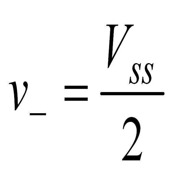
도 1b는 상기와 같은 열적 저항(rt)과 전계에 의해 변화되는 탐침의 저항(rRP)이 고려된 저항성 탐침의 등가회로이다. 이러한 등가회로에 따르면 출력(Vo)은 아래의 공식에 의해 얻어 진다. 아래의 식에서 R 은 바이어스 저항이며 Vss 는 바이어스 전압이다.FIG. 1B is an equivalent circuit of a resistive probe in consideration of the thermal resistance r t and the resistance of the probe r RP changed by an electric field. According to this equivalent circuit, the output Vo is obtained by the following formula. In the equation below, R is the bias resistor and Vss is the bias voltage.

위의 공식을 통해서 열적 저항(rt) 변화는 출력에 영향을 미친다는 점을 알수 있다. 본 발명은 출력(Vo)에서 열적 저항변화에 의한 성분을 분리하여 SNR을 향상시킨다.The above formula shows that the change in thermal resistance (r t ) affects the output. The present invention improves SNR by separating components due to thermal resistance change at the output Vo.
도 2a는 본 발명에 따른 정보 재생 장치의 개략적 구성을 보이는 도면이다.2A is a diagram showing a schematic configuration of an information reproducing apparatus according to the present invention.
분극 도메인에 의해 정보를 저장하는 강유전체 미디어(10)에 대해 전계효과 반도체 팁(31)을 갖는 반도체 탐침(30)이 소정 간격을 두고 배치된다. 탐침(30)으로 부터의 출력은 신호검출부(20)로 연결되고 신호검출부(20)는 복조기(DEMODULATOR, 50)로 연결되어 있다. 여기에서 신호검출부(20)는 일종의 신호 전처리 부분으로서 탐침에서의 전류 변화로부터 정보 신호가 실려 있는 변조신호를 추출한다. 그리고 탐침(30)에는 미디어(10)의 분극에 의해 포획된 전하에 의해 유기된 전류 변화 즉, 상기 정보 신호를 변조하는 변조기(MODULATOR, 40)가 연결된다. 상기 변조기(40)는 소정 주파수의 정현파를 발생하며 반도체 팁(31)[(30)]의 채널 영역에 변조 전계를 형성한다. 변조 전계에 의하[면]여 상기 정보 신호가 변조된다. 상기 신호검출부(20)는 상기 변조된 신호를 포함하여 상기 반도체탐침(30)으로 부터 발생된 신호를 검출하여 복조기(50)를 통과시킨다. 검출된 신호는 상기 복조기(50)를 통과하면서 상기 변조기(40)에 의하여 변조된 신호만을 분리 복조한다. 즉, 본 발명에 따르면, 고주파 변호 신호에 의해 정보 신호가 변조되고 열적 저항 변화에 따른 잡음 신호는 변조되지 않고, 따라서 상기 복조부에서 상기 정보 신호와 잡음 신호가 분리된다.The semiconductor probes 30 having the field
정보신호와 잡음신호의 분리, 즉 정보 신호의 변조 및 복조에 대해서는 후에 상세히 설명된다. 한편, 상기 신호검출부(20)에는 탐침(30)에 구동전압이 인가되도록 바이어스 전압(Vss)를 인가한다. 바이어스 전압은 신호검출부(20)를 경유하지 않고 상기 탐침(30)에 직접 인가될 수 있다. 바이어스 전압은 전계 효과 반도체 탐침이 기록매체의 정보를 읽어들이는 프루브로서 동작하기 위해 필요한 전압이다. The separation of the information signal and the noise signal, that is, the modulation and demodulation of the information signal will be described later in detail. Meanwhile, a bias voltage Vss is applied to the
위에서 설명된 도 2a의 구조를 본 발명에 따른 정보 재생 장치의 구성요소들은 기능적으로 분리한 것으로 설계에 의해 기능이 통합되고 이러한 재생장치에는 추가적인 기능이 더 포함될 수 있다.2A described above, the components of the information reproducing apparatus according to the present invention are functionally separated, and their functions are integrated by design, and such reproducing apparatus may further include additional functions.
상기 탐침(30)은 종래에 알려진 전계 효과 트랜지스터형 탐침이 적용된다. 예를 들어 미국특허 6,521,921에 개시된 전계 효과 트랜지스터 채널 구조가 형성된 주사 탐침(Scanning probe having field effect transistor channel)이나 미국공개특허 2005/0231225A1에 개시된 저항적 팁을 가지는 반도체 프로브(Semiconductor probe with resistive tip)을 이용할 수 있다.The
위의 두 종류의 종래 탐침뿐 아니라 다른 동종의 탐침이 본 발명의 재생장치 및 정보 재생 방법에 적용되기 위해서는 반도체 팁에 변조 전계가 형성할 수 있 는 구조를 가져야 하는데 대부분의 전계 효과 반도체 탐침은 이러한 조건을 갖추고 있다. 변조 전계를 형성하기 위한 구조 채널 영역에 전계를 형성하는 요소로서는 채널 영역에 변조 전계를 형성하는 기판 또는 이에 별도로 형성되는 전극이며 이 전극에 소정 주파수의 변조 신호가 인가된다. 변조 신호가 인가되는 전극(이하 변조 전극)은 반도체 팁이 형성되는 기판의 배면에 마련되거나 도 2b에서 개시된 바와 같이 켄틸레버의 일면에 마련될 수 있다. 변조 전극에 변조 신호가 인가되면 채널 영역에서 공핍층의 발생으로 전하 채널이 형성되게 되는데 변조 신호 강도에 따라 채널의 크기 즉 전류의 량이 변화되게 된다. In addition to the above two types of conventional probes, other types of probes must have a structure in which a modulated electric field can be formed on a semiconductor tip in order to be applied to the reproducing apparatus and information reproducing method of the present invention. I have a condition. Structure for forming a modulated electric field As an element for forming an electric field in a channel region, a substrate for forming a modulated electric field in a channel region or an electrode formed separately therefrom is a modulated signal of a predetermined frequency applied to the electrode. An electrode to which a modulation signal is applied (hereinafter, referred to as a modulation electrode) may be provided on the rear surface of the substrate on which the semiconductor tip is formed or on one surface of the cantilever as disclosed in FIG. 2B. When a modulation signal is applied to the modulation electrode, a charge channel is formed by the generation of a depletion layer in the channel region, and the size of the channel, that is, the amount of current, changes according to the modulation signal strength.
도 2b는 본 발명에 적용되는 탐침의 일종으로 미국공개특허 2005/0231225A1 에 개시된 프로브의 구조를 개략적으로 나타내고 있으며, 도 2c는 도 2b에 도시된 탐침의 팁 부분의 측단면을 나타내고 있다. FIG. 2B schematically illustrates the structure of a probe disclosed in US Patent Application Publication No. 2005 / 0231225A1 as a probe applied to the present invention, and FIG. 2C illustrates a side cross-sectional view of the tip portion of the probe shown in FIG. 2B.
도 2b를 참조하면, 도면을 참조하면, 실리콘 기판(33)의 상부에 절연층(37)이 적층되어 있으며, 절연층(37)의 상면에는 전극(39)이 형성되어 있다. 기판(33)의 표면의 실리콘층으로부터 캔티레버(35)가 연장되어 있으며, 캔티레버(35)의 선단 부분에 소스와 드레인 및 이 사이의 채널영역을 갖는 반도체 팁(31)이 형성되어 있다. 팁(31)의 경사면에는 트랜지스터의 소스와 드레인를 전기적으로 접촉된 소스, 드레인 전극(32, 34)이 형성되어 있다. 팁(30)의 첨두부에는 제2불순물이 저농도 도핑되어 약간의 이동도를 갖는 저항성 채널영역(36)이다. 소스, 드레인 전극(32, 34)은 캔티레버(35)를 통해 패드(39, 39)와 연결된다. 전술한 바와 같이 상기 채널 영역(36)은 전계에 의해서만 채널이 형성되거나 불순물이 약하게 도핑되어 무 전계시에도 약간의 이동도가 주어질 수 있다. 여기에서 상기 기판(33)에 변조기(40)의 한 구성요소인 변조신호발생부(41)가 연결될 수 있다. 보다 효과적인 변조 신호(vsub)의 인가를 위하여, 도 2b 및 도 2c에 도시된 바와 같이 상기 기판(33)에서 연장된 캔티레버(35)의 일면에 변조전극(35a)이 형성될 수 있다. 도 2a에서 변조기(40)에 상기 변조전극(35a)를 포함하여 표현한 것은 신호변조가 탐침의 반도체 팁에서 이루고 따라서 탐침의 일부 기능이 변조기에 포함되기 때문이다. 이러한 저항성 반도체 팁의 구조 및 동작은 미국공개특허 2005/0231225A1를 참조하면 충분히 이해될 수 있다.Referring to FIG. 2B, referring to the drawing, an insulating
도 3은 저항성 반도체 팁에서의 신호변조를 설명하는 도면이다.3 illustrates signal modulation in a resistive semiconductor tip.
기판(substrate)에 p 층이 형성되어 있고 p층의 표면에 n형 소스, 드레인 및 이사이에 약하게 도핑된 n- 채널영역이 마련되어 있다. 기판에는 소정 주파수의 정현파가 인가되어 채널영역에는 정현파에 의한 이동도의 변화가 일어난다. 이때에 미디어로 부터의 전계(field)가 인가되면 미디어로부터의 전계가 채널 영역 인가되어 정현파에 의한 이동도 변화가 나타나는 채널 영역의 이동도의 변화 폭이 확장된다. 즉, 전계에 의한 이동도는 정현파에 의해 증폭되며 이때에 증폭된 신호, 즉 변조된 신호가 출력하게 된다. 이때에 전계 의한 신호만이 증폭되고 전술한 바와 같은 열적 변화에 의해 발생되는 이동도의 변화 즉 열적 저항 변화(전류변화)에는 상기 변조 정현파가 영향을 미치지 못한다. 이러한 변조에 의하면 열적 변화에 의한 저항변화에 비해 전계변화에 의한 저항변화 즉 미디어로부터 얻어진 정보신호를 보 다 크게 증폭할 수 있게 된다.The p layer is formed on the substrate, and the n-channel region lightly doped with n-type source, drain and moving is provided on the surface of the p layer. A sinusoidal wave of a predetermined frequency is applied to the substrate, and the mobility of the sinusoidal wave is changed in the channel region. At this time, when a field from the media is applied, an electric field from the media is applied to the channel region, and the variation in the mobility of the channel region in which the mobility change due to the sine wave appears is expanded. That is, the mobility by the electric field is amplified by the sine wave, and the amplified signal, that is, the modulated signal is output. At this time, only the signal by the electric field is amplified, and the modulation sine wave does not affect the change in mobility generated by the thermal change as described above, that is, the change in thermal resistance (current change). According to such modulation, the change in resistance due to electric field change, that is, the information signal obtained from the media can be amplified more than the change in resistance due to thermal change.
이하의 구체적인 실시예를 통해서 본 발명의 정보 재생 장치 및 정보 재생 방법에 대해 이해할 수 있다.Through the following specific embodiments, it is possible to understand the information reproducing apparatus and the information reproducing method of the present invention.
도 4는 본 발명에 한 실시예에 따른 정보 재생 장치의 개략적 회로도이다.4 is a schematic circuit diagram of an information reproducing apparatus according to an embodiment of the present invention.
도 4에 도시된 실시예의 신호검출부(20)는 제 1 저항(R1)과 저항성 반도체 탐침(30)의 저항성분(rw )가 직렬로 연결된 하프 브릿지(half bridge)회로를 구성하여 상기 반도체 탐침(30)에 바이어스 전압(Vss)를 분배 인가하여 정보 재생 신호를 상기 제 1 저항(R1)과 저항성 반도체 탐침(30)의 저항성분(rw )이 연결된 노드에서 검출한다. 상세하게는 탐침(30) 끝에 형성되어 있는 전계 효과 반도체 팁(31)의 드레인 전극(34)은 상기 제1저항(R1)에 연결되고, 상기 하프 브릿지는 바이어스 전압(Vss)가 인가된다. 여기에서 기판(33) 바람직하게는 변조전극(35a)에는 변조신호발생부(41)로 부터 변조 전압 또는 변조신호(vsub)가 인가된다. The
상기 제 1 저항(R1)과 저항성 반도체 탐침(30)의 저항성분(rw )이 연결된 노드에서 출력된 신호(vo)는 복조기(40)로 연결된다. 복조기(40)는 입력된 신호에 대해 곱셈 연산하는 멀티플라이어(MPL)와 필터 예를 들어 저역통과필터(LPF)를 통해 최종 획득된 정보 신호를 출력한다.The signal v o output from the node connected to the first resistor R1 and the resistive component r w of the
상기한 바와 같이 본 발명의 정보 재생 장치 및 방법은 SNR을 높이기 위하여 정보신호의 변조 및 복조 과정을 거침으로써 열적 저항 변화에 의해 노이즈 신호를 분리 복조한다. 좀더 구체적으로 살펴보면 아래와 같다.As described above, the information reproducing apparatus and method of the present invention performs demodulation and demodulation of the information signal in order to increase the SNR, and separately demodulates the noise signal by the change in the thermal resistance. More specifically, it is as follows.
탐침(30)의 저항성 반도체 팁(31)은 미디어에 의해 유기되는 전계를 검출하여 이에 따라 이동도 즉 전기적 저항이 바뀐다. 팁(31)과 미디어 간의 간격은 미디어의 표면 거칠기에 의해 변화되고 따라서 열의 방출량이 변하고 따라서 이에 따른 이동도의 변화로 저항의 변화가 나타난다. 따라서 저항성 탐침의 총저항(rw)은 반도체 팁(31)의 순저항 성분(Ro), 미디어로 부터의 전계 변화에 의해 변화되는 저항 성분(rf) 그리고 열적인 불안적성 기인한 저항 성분(rt)의 합으로 결정된다. 전술한 제1저항기(R1)은 상기 순저항 성분과 같은 값(Ro)을 가지며, 상기 변조신호(vsub)는 소정 주파수(ω)의 정현파이다. 여기에서 변조신호의 전압(vsub)은 아래와 같이 계산된다.The
![]()
![]()
이때 상기 반도체 탐침에 분배 인가되는 노드 전압 vo는 다음과 같이 계산된다.At this time, the node voltage v o distributed to the semiconductor probe is calculated as follows.

여기서 전계에 의하여 바뀌는 저항 성분 rf 의 위첨자 ω는 변조 전압 vsub의 주파수ω로 변조되었음을 의미한다.Here, the superscript ω of the resistance component r f, which is changed by the electric field, is modulated by the frequency ω of the modulation voltage v sub .
위 출력전압 vo 로부터 전계에 의하여 바뀌는 저항 성분 rf을 뽑아내기 위하여 복조기(50)를 사용한다. 복조기(50)는 멀티플라이어(51)와 저역 통과 필터(low-pass filter)(52)를 포함한다. 상기 변조신호(vsub)와 동일한 주파수를 가지고 상기 출력 전압 vo 와 위상이 같은 복조신호(vsub' )와 상기 출력 vo 을 상기 멀티플라이어(51)를 이용하여 곱하면 아래와 같은 출력 전압 vom 이 얻어진다.The

여기서 각 저항 성분의 위 첨자는 0, ω, 2ω 의 주파수 성분임을 표시한다.Here, the superscript of each resistance component indicates that it is a frequency component of 0, ω, and 2ω.
따라서 상기 출력전압 vom 을 저역 통과 필터(52)를 통과시켜 상기 변조신호의 주파수 ω 성분을 갖지 않는 직류 성분(rf 0)만을 검출하면 전계에 의하여 바뀌는 저항 성분 rf만 을 검출할 수 있게 된다. Therefore, when the output voltage v om is passed through the
도 5는 본 발명의 다른 실시예에 따른 정보 재생 장치의 개략적 회로도이다.5 is a schematic circuit diagram of an information reproducing apparatus according to another embodiment of the present invention.
도 5에 도시된 실시예의 정보 재생장치는 변조 신호의 검출이 두 개의 브랜치를 가지는 휘트스톤 브릿지에 의해 이루어진다. 도면에서 좌측 브랜치는 직렬로 연결되는 저항성 반도체 팁(31)과 제1저항기(R)에 의해 구성되며 우측 브랜치는 제2저항기(R2) 및 제3저항(R3)에 의해 구성된다. 탐침(30) 끝에 형성되어 있는 저항성 반도체 팁(31)의 드레인 전극(34)은 접지되고, 소스 전극(32)은 상기 제1저항(R1)에 연결된다. 직렬의 제2저항기(R2)과 제3저항기(R3)에 의한 브랜치에서 제3저항기(R3)에 의해 접지된다. 휘트스톤 브리지의 좌측 브랜치와 우측 브랜치에는 공히 바이어스 전압(Vss)이 인가된다.In the information reproducing apparatus of the embodiment shown in Fig. 5, the detection of the modulated signal is made by a Wheatstone bridge having two branches. In the drawing, the left branch is formed by the
여기에서 기판(33)에, 바람직하게는 변조전극(35a)에는 변조신호발생부(41)로 부터 변조 전압 또는 변조신호(vsub)가 인가된다. 제1저항기(R1)와 소스 전극(32) 사이의 노드(P1)와 제2저항(R2)과 제3저항(R3)간의 노드(P2)는 차동 증폭기(21)의 비반전(+) 입력단과 반전(-)입력단에 각각 연결된다. 차동 증폭기(21)의 출력단은 복조기(50)로 연결된다. 복조기(50)는 멀티플라이어(MPL)와 필터 예를 들어 저역통과필터(LPF)를 통해 최종 획득된 정보 신호를 출력한다. Here, the modulation voltage or the modulation signal v sub is applied to the
상기한 바와 같이 본 발명의 정보 재생 장치 및 방법은 SNR을 높이기 위하여 정보신호의 변조 및 복조 과정을 거침으로써 열적 저항 변화에 의해 노이즈 신호를 분리 복조한다. 좀더 구체적으로 살펴보면 아래와 같다.As described above, the information reproducing apparatus and method of the present invention performs demodulation and demodulation of the information signal in order to increase the SNR, and separately demodulates the noise signal by the change in the thermal resistance. More specifically, it is as follows.
탐침(30)의 저항성 반도체 팁(31)은 미디어에 의해 유기되는 전계를 검출하여 이에 따라 이동도 즉 전기적 저항이 바뀐다. 팁(31)과 미디어 간의 간격은 미디어의 표면 거칠기에 의해 변화되고 따라서 열의 방출량이 변하고 따라서 이에 따른 이동도의 변화로 저항의 변화가 나타난다. 따라서 저항성 탐침의 총저항(rw)은 반도 체 팁(31)의 순저항 성분(Ro), 미디어로 부터의 전계 변화에 의해 변화되는 저항 성분(rf) 그리고 열적인 불안적성 기인한 저항 성분(rt)의 합으로 결정된다. 전술한 제1저항기(R1)은 상기 순저항 성분과 같은 값(Ro)을 가지고, 상기 제 2 저항기(R2)는 상기 제 3 저항기(R3)와 같은 값을 가지며, 상기 변조신호(vsub)는 소정 주파수(ω)의 정현파이다. 여기에서 변조신호의 전압(vsub)은 아래와 같이 계산된다.The
![]()
![]()
이때 브릿지의 노드 전압 v+는 다음과 같이 계산된다.At this time, the node voltage v + of the bridge is calculated as follows.

여기서 전계에 의하여 바뀌는 저항 성분 rf 의 위첨자 ω는 변조 전압 vsub의 주파수 ω로 변조되었음을 의미한다. 오프셋(offset) 전압을 제거하기 위하여 저항 R2 저항 R3에 의해 휘트스톤 브릿지의 한쪽 브랜치가 형성된다. 이 때 브랜치의 노드 전압 v-는 다음과 같다. Here, the superscript ω of the resistance component r f changed by the electric field means that the modulation is performed at the frequency ω of the modulation voltage v sub . One branch of the Wheatstone bridge is formed by the resistor R2 resistor R3 to eliminate the offset voltage. At this time, the node voltage v − of the branch is as follows.
양 브랜치의 노드 전압 v+와 v-를 이득 A를 가지는 차동 증폭기(10)을 이용하여 증폭하면 출력 전압 vo는 다음의 값을 가진다. Amplifying the node voltages v + and v - of both branches using the

위 전압 vo 로부터 전계에 의하여 바뀌는 저항 성분 rf을 뽑아내기 위하여 복조기(50)를 사용한다. 복조기(50)는 멀티플라이어(51)와 저역 통과 필터(low-pass filter)(52)를 포함한다. 차동 증폭기(21)의 출력 vo과 상기 변조신호(vsub)와 동일한 주파수를 가지고 상기 출력 전압 vo 와 위상이 같은 복조신호(vsub' )를 멀티플라이어(51)를 이용하여 곱하면 아래와 같은 출력 전압 vom 이 얻어진다.The

여기서 각 저항 성분의 위 첨자는 0, ω, 2ω 의 주파수 성분임을 표시한다.Here, the superscript of each resistance component indicates that it is a frequency component of 0, ω, and 2ω.
따라서 저역 통과 필터(52)를 이용하여 직류 성분만을 검출하면 전계에 의하여 바뀌는 저항 성분 rf만 을 검출할 수 있게 된다. Therefore, if only the direct current component is detected using the
이하에서는 본 발명의 다른 실시예에 따른 정보 재생 장치 및 방법에 대해 설명한다.Hereinafter, an information reproducing apparatus and method according to another embodiment of the present invention will be described.
도 6를 참조하면, 상기 반도체 탐침으로 궤환루우프를 형성한 연산증폭기를 포함한 반전증폭회로를 사용하여 반도체 탐침에 전압을 분배 인가하고 연산증폭기의 출력단에서 신호를 검출할 수 있다. 저항성 탐침(30)의 선단에 마련된 저항성 반도체 팁(31)의 소스 전극(32)은 연산증폭기(21)의 출력단에 연결되고 드레인 전극(34)은 연산증폭기(21)의 반전 입력단(-)에 연결되어 있다. 상기 연산 증폭기(21)의 반전입력단에는 제1 저항기(R1)가 각각 접속되고 바이어스(Vss)가 인가된다. 이에 더하여 비반전 입력단(+)은 접지된다. 상기 연산 증폭기(21)의 출력단은 복조기(50)에 연결된다. 복조기(50)는 멀티플라이어(51)와 필터 예를 들어 저역통과필터(52)를 갖는다.Referring to FIG. 6, a voltage may be dividedly applied to a semiconductor probe by using an inverted amplifier circuit including an operational amplifier having a feedback loop formed by the semiconductor probe, and a signal may be detected at an output terminal of the operational amplifier. The source electrode 32 of the
상기한 바와 같이 반도체 팁(31)의 총저항(Rw)은 정상적 저항(nominal resistance) R0와 전계에 의해 변화되는 rf와 열변화에 따른 저항 성분 rt의 합으로 결정된다. 제1저항은 상기 반도체 팁의 정상 저항(R0)과 같은 값을 가진다. 기판(33) 또는 변조전극(35a)에는 소정 주파수(ω)의 정현파인 변조신호 또는 변조 전압(vsub)가 인가된다.As described above, the total resistance Rw of the
![]()
![]()
여기에서, 상기 비반전 입력단에서의 임피던스는 무한대이므로 여기서의 전류 방정식을 통해 연산증폭기(21)의 출력 전압 vo을 구하면 다음과 같다.Here, since the impedance at the non-inverting input terminal is infinite, the output voltage vo of the

여기서 전계에 의하여 바뀌는 저항 성분 rf의 위첨자는 변조전압 vsub의 주파수 ω로 변조되었음을 의미한다. 위 전압으로부터 전계에 의하여 바뀌는 저항 성분 rf은 복조기(50)로 부터 얻어진다. 복조기(50)는 멀티플라이어(51)와 저역 통과 필터(52)를 포함한다. 상기 연산 증폭기(21)의 출력 vo과 상기 변조신호(vsub)와 동일한 주파수를 가지고 상기 출력 전압 vo 와 위상이 같은 복조신호(vsub' )를 멀티플라이어를 이용해 곱하면 다음과 같은 출력 전압 vom을 얻을 수 있다.Here, the superscript of the resistance component r f changed by the electric field means that the modulation is performed at the frequency ω of the modulation voltage v sub . The resistance component r f, which is changed by the electric field from the above voltage, is obtained from the

여기서 각 저항 성분의 위 첨자 0, ω, 2ω는 주파수 성분임을 표시한다. 따라서 저역 통과 필터(52)를 이용하여 필터링하며 전계에 의하여 바뀌는 저항 성분 rf만을 검출할 수 있게 된다.Here, the
상기한 바와 같이 본 발명은 열적 변화에 따른 잡음 신호가 혼재하는 반도체 팁으로 부터의 신호를 소정 주파수의 변조 신호를 가하여 전계에 의해 변하는 저항에 의한 신호만을 변조하고 이를 복조함으로써 열적 잡음 신호가 없는 순수한 정보 신호를 얻을 수 있게 된다.As described above, the present invention applies a modulated signal of a predetermined frequency to a signal from a semiconductor tip in which a noise signal due to a thermal change is mixed, and modulates only a signal by a resistance that is changed by an electric field, thereby demodulating the pure signal without a thermal noise signal. An information signal can be obtained.
도 7를 참조하면, 저항성 탐침(30)의 선단에 마련된 저항성 반도체 팁(31)의 소스 전극(32)은 연산증폭기(21)의 출력단에 연결되고 드레인 전극(34)은 연산증폭기(21)의 반전 입력단(-)에 연결되어 있다. 연산 증폭기(21)의 반전입력단과 비반적 입력단에는 제1,2저항기(R1, R2)가 각각 접속되고 이들에 공히 바이어스 전압(Vss)가 인가된다. 이에 더하여 비반전 입력단(+)에 상기 제2저항기(R)와 전압 분배부를 구성하는 제3저항기(R)가 접속된다. 상기 연산[차동] 증폭기(21)의 출력단은 복조기(50)에 연결된다. 복조기(50)는 멀티플라이어(51)와 필터 예를 들어 저역통과필터(52)를 갖는다.Referring to FIG. 7, the
상기한 바와 같이 반도체 팁(31)의 총저항(Rw)은 정상적 저항(nominal resistance) R0와 전계에 의해 변화되는 rf와 열변화에 따른 저항 성분 rt의 합으로 결정된다. 제1저항은 상기 반도체 팁의 정상 저항 R0과 같은 값을 가진다. 기판(33) 또는 변조 전극(33a)에는 소정 주파수(ω)의 정현파인 변조신호 또는 변조 전압 (vsub)가 인가된다.As described above, the total resistance Rw of the
![]()
![]()
여기에서, 비반전 입력단과 반전입력단에 전위 V+, V-는 아래와 같다.Here, the potentials V + and V- at the non-inverting input terminal and the inverting input terminal are as follows.


상기 비반전 입력단에서의 임피던스는 무한대이므로 여기서의 전류 방정식은 다음과 같다.Since the impedance at the non-inverting input terminal is infinite, the current equation is as follows.

이때에 연산 증폭기(21)의 출력 전압은 다음과 같다.At this time, the output voltage of the

여기서 전계에 의하여 바뀌는 저항 성분 rf의 위첨자는 변조전압 vsub의 주파수 ω로 변조되었음을 의미한다. 위 전압으로부터 전계에 의하여 바뀌는 저항 성분 rf은 복조기(50)로 부터 얻어진다. 복조기(50)는 멀티플라이어(51)와 저역 통과 필터(52)를 포함한다. 연산 증폭기(21)의 출력 vo과 변조전압 vsub를 멀티플라이어를 이용해 곱하면 다음과 같은 출력 전압 vom을 얻을 수 있다.Here, the superscript of the resistance component r f changed by the electric field means that the modulation is performed at the frequency ω of the modulation voltage v sub . The resistance component r f, which is changed by the electric field from the above voltage, is obtained from the

여기서 각 저항 성분의 위 첨자 0, ω, 2ω는 주파수 성분임을 표시한다. 따라서 저역 통과 필터(52)를 이용하여 필터링하며 전계에 의하여 바뀌는 저항 성분 rf만을 검출할 수 있게 된다.Here, the
상기한 바와 같이 본 발명은 열적 변화에 따른 잡음 신호가 혼재하는 반도체 팁으로 부터의 신호를 소정 주파수의 변조 신호를 가하여 전계에 의해 변하는 저항에 의한 신호만을 변조하고 이를 복조함으로써 열적 잡음 신호가 없는 순수한 정보 신호를 얻을 수 있게 된다.As described above, the present invention applies a modulated signal of a predetermined frequency to a signal from a semiconductor tip in which a noise signal due to a thermal change is mixed, and modulates only a signal by a resistance that is changed by an electric field, thereby demodulating the pure signal without a thermal noise signal. An information signal can be obtained.
도 8은 본 발명에 따른 반도체 탐침을 이용한 정보 재생 방법에 대한 절차를 개략적으로 나타낸 것이다. 8 schematically illustrates a procedure for an information reproducing method using a semiconductor probe according to the present invention.
매체에 기록된 정보에 의하여 발생하는 전기장은 상기 정보 매체의 표면에 트랩된 전하 또는 다이폴 모멘트에 의해 발생한다. 상기 전기장에 의하여 반도체 탐침의 채널영역이 변하여 탐침(30)의 저항이 변한다. 탐침(30)에 구동전압을 가하여 발생하는 신호는 탐침의 순저항성분과 상기 전기장에 의하여 변동되는 저항성분과 열저항변동 성분에 의한 것으로 나눌 수 있다.The electric field generated by the information recorded on the medium is generated by the charge or dipole moment trapped on the surface of the information medium. The resistance of the
변조단계(40)에서는 상기 반도체 탐침(30)에 고주파변조신호(Vsub)를 가하여 변조 전계를 형성하여 상기 전기장에 의해 변동되는 저항성분 신호만을 변조한다.In the
신호검출단계(20)에서 반도체 탐침에 구동전압을 가하여 검출하는 신호에는 상기 변조신호에 의하여 변조된 신호, 즉 전기장에 의해 변동되는 변조된 저항성분 신호와 탐침의 순저항성분, 열저항변동 성분의 신호의 합으로 표현될 수 있다. In the
상기 신호검출단계(20)는 상기 반도체 탐침에 바이어스전압(Vss)을 분배하여 상기 반도체 탐침에서 발생하는 신호를 추출하도록 전압분배회로로 구성될 수 있으며, 상기 전압분배회로로 브리지 회로를 사용하거나 궤한 루프를 가진 연산증폭 회로를 사용하기도 한다. 이때 전압 분배시 발생하는 오프셋 전압을 제거하는 단계와 검출 신호를 증폭하는 단계를 더 포함하기도 한다. 이에 대한 상세한 내용은 도 4 내지 도 7의 설명에서 이미 서술한 바 있다. The
복조단계(50)는 상기 신호검출단계에서 검출된 신호에서 상기 변조 전계에 의해 변조된 정보신호를 추출하는 단계로, 상기 신호검출단계에서 검출된 신호와 복조신호를 곱하는 단계와; 상기 곱하는 단계로부터 출력된 신호로부터 소정의 주파수보다 작은 주파수 영역의 신호를 추출하는 단계를 포함한다. 상기 복조신호는 상기 변조신호와 주파수가 대체로 동일하고 상기 신호검출단계에서 검출된 신호와 위상이 대체로 같다. 이에 대한 상세한 내용 역시 도 4 내지 도 7의 설명에서 이미 서술한 바 있다.The demodulation step (50) is a step of extracting the information signal modulated by the modulation electric field from the signal detected in the signal detection step, multiplying the signal detected in the signal detection step and the demodulation signal; And extracting a signal of a frequency domain smaller than a predetermined frequency from the signal output from the multiplying step. The demodulated signal has substantially the same frequency as the modulated signal and has substantially the same phase as the signal detected in the signal detection step. Details thereof have already been described in the description of FIGS. 4 to 7.
도 9 및 도 10은 전술한 휘트스톤 브릿지 및 차동 증폭기를 신호 검출부로하고 이용한 도 5에 개시된 실시예의 시뮬레이션 결과를 각각 보인다.9 and 10 show simulation results of the embodiment disclosed in FIG. 5 using the Wheatstone bridge and the differential amplifier as the signal detectors, respectively.
도 9에서, 첫번째 파형도(1)는 전계에 의해 바뀌는 저항 rf의 파형, 두번째 파형도(2)는 열변화에 따른 저항성분 rt (단일 정현파로 간주함)의 파형, 세번째 파형도(3)는 차동증폭기의 출력 파형, 네 번째 파형도(4)는 차동증폭기의 출력을 복조하여 전계에 의해 변화되는 저항 변화파형을 보인다.In FIG. 9, the first waveform diagram 1 is the waveform of the resistance r f changed by the electric field, the second waveform diagram 2 is the waveform of the resistance component r t (referred to as a single sine wave) according to the thermal change, and the third waveform diagram ( 3) shows the output waveform of the differential amplifier, and the fourth waveform diagram (4) shows the resistance change waveform changed by the electric field by demodulating the output of the differential amplifier.
도 10은 열변화에 따른 저항 변화가 주파수가 서로 다른 3개의 정현파의 합으로 가정한 경우의 시뮬레이션 결과는 보인다. 즉, 도 10에서, 첫번째 파형도(1)는 전계에 의해 바뀌는 저항 rf의 파형, 두번째 파형도(2)는 열변화에 따른 저항성분 rt (3개의 정현파가 합성된 합성파로 간주함)의 파형, 세번째 파형도(3)는 차동증폭기의 출력 파형, 네 번째 파형도(4)는 차동증폭기의 출력을 복조하여 전계에 의해 변화되는 저항 변화파형을 보인다.FIG. 10 shows simulation results when the resistance change due to heat change is assumed to be the sum of three sinusoids having different frequencies. That is, in FIG. 10, the first waveform diagram 1 is the waveform of the resistance r f changed by the electric field, and the second waveform diagram 2 is the resistance component r t according to the thermal change (referred to as a synthesized wave in which three sinusoidal waves are synthesized). The third waveform diagram (3) shows the output waveform of the differential amplifier, and the fourth waveform diagram (4) shows the resistance change waveform which is changed by the electric field by demodulating the output of the differential amplifier.
상기와 같은 본 발명에 의하면, 열적 불안정성에 기인한 잡음 신호로 부터 미디어로 부터 얻어진 정보 신호를 성공적으로 얻어 낼 수 있고, 특히 변조 및 복조의 과정을 통해서 SNR을 높일 수 있으므로 보다 감도높게 정보를 재생할 수 잇다.According to the present invention as described above, the information signal obtained from the media can be successfully obtained from the noise signal due to thermal instability, and in particular, since the SNR can be increased through the process of modulation and demodulation, the information can be reproduced more sensitively. Can be.
상술한 바와 같이, 본 발명에 따르면 변조에 의해 전계변화에 의한 신호와 열적 변화에 신호를 분리하여 유효한 정보신호를 검출함으로써 SNR이 향상되고 이로 인해 열적 잡음에 불구하고 정보신호를 안정적으로 재생할 수 있다.As described above, according to the present invention, the SNR is improved by separating the signal due to the electric field change and the thermal change by the modulation and detecting the effective information signal, thereby stably reproducing the information signal despite the thermal noise. .
이러한 본 발명은 전계 효과 트랜지스터형 탐침이 이용되는 다양한 분야에 적용될 수 있고 특히 정보 재생 분야에 적용되기 바람직하다.The present invention can be applied to various fields in which a field effect transistor type probe is used, and is particularly preferable to the field of information reproduction.
상기와 같은 실시예를 통해서, 본 발명이 속하는 기술 분야에서 통상의 지식을 가진 자라면 본 발명의 기술적 사상에 의해 다양한 형태의 탐침을 이용하여 정보를 기록 및 재생할 수 있는 장치를 제조할 수 있을 것이다. 때문에 본 발명의 범위는 설명된 실시예에 의하여 정하여 질 것이 아니고 특허 청구범위에 기재된 기술적 사상에 의해 정하여져야 한다.Through the above embodiments, those skilled in the art will be able to manufacture a device capable of recording and reproducing information using various types of probes by the technical idea of the present invention. . Therefore, the scope of the present invention should not be defined by the described embodiments, but should be determined by the technical spirit described in the claims.
Claims (20)
Priority Applications (4)
| Application Number | Priority Date | Filing Date | Title |
|---|---|---|---|
| KR1020060002370A KR100682956B1 (en) | 2006-01-09 | 2006-01-09 | Method for reproducing information using semiconductor probe and device adopting the same |
| CN2006101428055A CN101000782B (en) | 2006-01-09 | 2006-10-26 | Method of reproducing information using semiconductor probe and device adopting the semiconductor probe |
| JP2006348074A JP4503587B2 (en) | 2006-01-09 | 2006-12-25 | Information reproducing method using semiconductor probe and apparatus using the same |
| US11/650,940 US7746753B2 (en) | 2006-01-09 | 2007-01-09 | Method of reproducing information using semiconductor probe and device adopting the semiconductor probe |
Applications Claiming Priority (1)
| Application Number | Priority Date | Filing Date | Title |
|---|---|---|---|
| KR1020060002370A KR100682956B1 (en) | 2006-01-09 | 2006-01-09 | Method for reproducing information using semiconductor probe and device adopting the same |
Publications (1)
| Publication Number | Publication Date |
|---|---|
| KR100682956B1 true KR100682956B1 (en) | 2007-02-15 |
Family
ID=38106413
Family Applications (1)
| Application Number | Title | Priority Date | Filing Date |
|---|---|---|---|
| KR1020060002370A KR100682956B1 (en) | 2006-01-09 | 2006-01-09 | Method for reproducing information using semiconductor probe and device adopting the same |
Country Status (4)
| Country | Link |
|---|---|
| US (1) | US7746753B2 (en) |
| JP (1) | JP4503587B2 (en) |
| KR (1) | KR100682956B1 (en) |
| CN (1) | CN101000782B (en) |
Cited By (1)
| Publication number | Priority date | Publication date | Assignee | Title |
|---|---|---|---|---|
| US8339926B2 (en) | 2008-06-24 | 2012-12-25 | Seagate Technology Llc | Electric field read/write apparatus and method |
Families Citing this family (6)
| Publication number | Priority date | Publication date | Assignee | Title |
|---|---|---|---|---|
| US20090168636A1 (en) * | 2007-12-31 | 2009-07-02 | Tsung-Kuan Allen Chou | Cantilever design with electrostatic-force-modulated piezoresponse force microscopy (pfm) sensing |
| US20100116038A1 (en) * | 2008-11-12 | 2010-05-13 | International Business Machines Corporation | Feedback- enhanced thermo-electric topography sensing |
| US8922227B2 (en) * | 2011-03-08 | 2014-12-30 | Freescale Semiconductor Inc. | Systems and methods for detecting surface charge |
| US9678137B2 (en) * | 2014-02-26 | 2017-06-13 | Dell Products L.P. | System and method to monitor contact joint integrity |
| US9784787B2 (en) * | 2015-04-15 | 2017-10-10 | Nxp Usa, Inc. | Electric field sensor, system, and method for programming electronic devices on a wafer |
| CN105571727B (en) * | 2015-12-15 | 2018-10-02 | 清华大学 | The signal reading method and read-out system of graphene thermopile device |
Citations (5)
| Publication number | Priority date | Publication date | Assignee | Title |
|---|---|---|---|---|
| JP2000268421A (en) * | 1999-03-12 | 2000-09-29 | Canon Inc | Prove for recording and reproduction and recording and reproducing device composed of same probe |
| US6477132B1 (en) * | 1998-08-19 | 2002-11-05 | Canon Kabushiki Kaisha | Probe and information recording/reproduction apparatus using the same |
| JP2003178947A (en) * | 2001-12-10 | 2003-06-27 | Hitachi Ltd | Probe drawing device, method, and insulation characteristics evaluation device |
| KR20040036379A (en) * | 2002-10-25 | 2004-04-30 | 엘지전자 주식회사 | Nano data storage system |
| KR20050026754A (en) * | 2003-09-06 | 2005-03-16 | 삼성전자주식회사 | Method of data storage device using probe technology |
Family Cites Families (11)
| Publication number | Priority date | Publication date | Assignee | Title |
|---|---|---|---|---|
| JP3064399B2 (en) * | 1990-11-14 | 2000-07-12 | オリンパス光学工業株式会社 | Scanning probe microscope image processor |
| JPH09282725A (en) * | 1996-04-10 | 1997-10-31 | Canon Inc | Information recording/reproducing device |
| US6913982B2 (en) * | 2001-05-08 | 2005-07-05 | Geunbae Lim | Method of fabricating a probe of a scanning probe microscope (SPM) having a field-effect transistor channel |
| JP2003296979A (en) * | 2002-01-31 | 2003-10-17 | Yasuo Cho | System of extracting recording condition of dielectric recording medium, recording condition extracting method and information recorder |
| KR100468850B1 (en) * | 2002-05-08 | 2005-01-29 | 삼성전자주식회사 | Semiconductor probe with resistive tip and Method of fabricating thereof and Information recording apparatus, Information reproducing apparatus, and Information measuring apparatus comprising the same |
| KR100499127B1 (en) * | 2002-07-05 | 2005-07-04 | 삼성전자주식회사 | High density information storage medium and method of manufacturing the same and information storage apparatus and method of writing, reading and erasing information utilizing the same |
| JP3954457B2 (en) * | 2002-07-09 | 2007-08-08 | パイオニア株式会社 | Dielectric recording medium and dielectric recording / reproducing apparatus |
| JP3954456B2 (en) * | 2002-07-09 | 2007-08-08 | パイオニア株式会社 | Pickup device |
| GB2415827B (en) | 2003-05-01 | 2006-08-30 | Pioneer Corp | Recording/reproducing head and recording/reproducing apparatus |
| US7423954B2 (en) * | 2003-12-17 | 2008-09-09 | Hewlett-Packard Development Company, L.P. | Contact probe storage sensor pod |
| KR100624434B1 (en) * | 2004-09-07 | 2006-09-19 | 삼성전자주식회사 | Semiconductor probe with resistive tip and methoc of fabricating the same |
-
2006
- 2006-01-09 KR KR1020060002370A patent/KR100682956B1/en not_active IP Right Cessation
- 2006-10-26 CN CN2006101428055A patent/CN101000782B/en not_active Expired - Fee Related
- 2006-12-25 JP JP2006348074A patent/JP4503587B2/en not_active Expired - Fee Related
-
2007
- 2007-01-09 US US11/650,940 patent/US7746753B2/en not_active Expired - Fee Related
Patent Citations (5)
| Publication number | Priority date | Publication date | Assignee | Title |
|---|---|---|---|---|
| US6477132B1 (en) * | 1998-08-19 | 2002-11-05 | Canon Kabushiki Kaisha | Probe and information recording/reproduction apparatus using the same |
| JP2000268421A (en) * | 1999-03-12 | 2000-09-29 | Canon Inc | Prove for recording and reproduction and recording and reproducing device composed of same probe |
| JP2003178947A (en) * | 2001-12-10 | 2003-06-27 | Hitachi Ltd | Probe drawing device, method, and insulation characteristics evaluation device |
| KR20040036379A (en) * | 2002-10-25 | 2004-04-30 | 엘지전자 주식회사 | Nano data storage system |
| KR20050026754A (en) * | 2003-09-06 | 2005-03-16 | 삼성전자주식회사 | Method of data storage device using probe technology |
Cited By (1)
| Publication number | Priority date | Publication date | Assignee | Title |
|---|---|---|---|---|
| US8339926B2 (en) | 2008-06-24 | 2012-12-25 | Seagate Technology Llc | Electric field read/write apparatus and method |
Also Published As
| Publication number | Publication date |
|---|---|
| CN101000782A (en) | 2007-07-18 |
| US20070159193A1 (en) | 2007-07-12 |
| JP4503587B2 (en) | 2010-07-14 |
| US7746753B2 (en) | 2010-06-29 |
| CN101000782B (en) | 2012-04-18 |
| JP2007184081A (en) | 2007-07-19 |
Similar Documents
| Publication | Publication Date | Title |
|---|---|---|
| KR100718154B1 (en) | Information media a method for writing and reproducing information, and device adopting the same | |
| KR100682956B1 (en) | Method for reproducing information using semiconductor probe and device adopting the same | |
| JP3073616B2 (en) | Information processing device with multiple probes | |
| US10001529B2 (en) | Low-offset Graphene Hall sensor | |
| JPWO2004097822A1 (en) | Recording/reproducing head and recording/reproducing apparatus | |
| US7385901B2 (en) | Data recording/reproducing apparatus and method using needle-shaped member | |
| US7852738B2 (en) | Method of improving sensitivity of electric field sensor, storage apparatus including electric field sensor, and method of reproducing information of the storage apparatus | |
| US20050128928A1 (en) | Recording / reproducing head, recording / reproducing head array, method of producing the same, and recording apparatus and reproducing apparatus | |
| US20100208573A1 (en) | Method and device for detecting ferroelectric polarization | |
| JP3135753B2 (en) | Recording / reproducing method and apparatus using probe | |
| US8339926B2 (en) | Electric field read/write apparatus and method | |
| KR100532336B1 (en) | Reading data in probe-based storage devices | |
| US5581538A (en) | Recording/reproducing apparatus with a probe to detect data recorded in pits and projections of a recording medium | |
| US20080170488A1 (en) | Method and device for non-destructive reading for a ferroelectric-material storage media | |
| Kim et al. | Scanning probe charge reading of ferroelectric domains | |
| KR100468823B1 (en) | High Density Data Storage with Diamond Tips and How It Works | |
| KR100634552B1 (en) | Electrical field sensing probe having separated sensor and information storing device having the same | |
| KR20040036379A (en) | Nano data storage system | |
| JPS6040504A (en) | Detecting circuit for resistance change | |
| JP3118654B2 (en) | Information processing device and scanning tunneling electron microscope | |
| Nishiguchi et al. | Room-temperature several-hundred-of-megahertz charge sensing with single-electron resolution using a silicon transistor | |
| JP2968610B2 (en) | Information recording / reproducing device | |
| KR20040036380A (en) | Data writing and reading system | |
| JPS58211345A (en) | Recording and reproducing system |
Legal Events
| Date | Code | Title | Description |
|---|---|---|---|
| A201 | Request for examination | ||
| E701 | Decision to grant or registration of patent right | ||
| GRNT | Written decision to grant | ||
| FPAY | Annual fee payment |
Payment date: 20120203 Year of fee payment: 6 |
|
| FPAY | Annual fee payment |
Payment date: 20130125 Year of fee payment: 7 |
|
| LAPS | Lapse due to unpaid annual fee |