KR100627139B1 - Micromechanical structures and Method thereof - Google Patents
Micromechanical structures and Method thereof Download PDFInfo
- Publication number
- KR100627139B1 KR100627139B1 KR1020040045258A KR20040045258A KR100627139B1 KR 100627139 B1 KR100627139 B1 KR 100627139B1 KR 1020040045258 A KR1020040045258 A KR 1020040045258A KR 20040045258 A KR20040045258 A KR 20040045258A KR 100627139 B1 KR100627139 B1 KR 100627139B1
- Authority
- KR
- South Korea
- Prior art keywords
- sacrificial layer
- oxide
- micromechanical
- hydrophilic
- layer
- Prior art date
Links
- 238000000034 method Methods 0.000 title claims description 45
- KRHYYFGTRYWZRS-UHFFFAOYSA-N Fluorane Chemical compound F KRHYYFGTRYWZRS-UHFFFAOYSA-N 0.000 claims abstract description 62
- VYPSYNLAJGMNEJ-UHFFFAOYSA-N Silicium dioxide Chemical compound O=[Si]=O VYPSYNLAJGMNEJ-UHFFFAOYSA-N 0.000 claims abstract description 37
- 229910052814 silicon oxide Inorganic materials 0.000 claims abstract description 37
- 238000005530 etching Methods 0.000 claims abstract description 30
- 238000004519 manufacturing process Methods 0.000 claims abstract description 16
- XLYOFNOQVPJJNP-UHFFFAOYSA-N water Substances O XLYOFNOQVPJJNP-UHFFFAOYSA-N 0.000 claims description 49
- 239000000463 material Substances 0.000 claims description 30
- 239000007789 gas Substances 0.000 claims description 24
- 229910052782 aluminium Inorganic materials 0.000 claims description 16
- XAGFODPZIPBFFR-UHFFFAOYSA-N aluminium Chemical compound [Al] XAGFODPZIPBFFR-UHFFFAOYSA-N 0.000 claims description 15
- XEEYBQQBJWHFJM-UHFFFAOYSA-N Iron Chemical compound [Fe] XEEYBQQBJWHFJM-UHFFFAOYSA-N 0.000 claims description 14
- UQSXHKLRYXJYBZ-UHFFFAOYSA-N Iron oxide Chemical compound [Fe]=O UQSXHKLRYXJYBZ-UHFFFAOYSA-N 0.000 claims description 14
- 239000010936 titanium Substances 0.000 claims description 14
- RTAQQCXQSZGOHL-UHFFFAOYSA-N Titanium Chemical compound [Ti] RTAQQCXQSZGOHL-UHFFFAOYSA-N 0.000 claims description 11
- 229910052719 titanium Inorganic materials 0.000 claims description 11
- TWNQGVIAIRXVLR-UHFFFAOYSA-N oxo(oxoalumanyloxy)alumane Chemical compound O=[Al]O[Al]=O TWNQGVIAIRXVLR-UHFFFAOYSA-N 0.000 claims description 10
- 239000003054 catalyst Substances 0.000 claims description 8
- 229910052804 chromium Inorganic materials 0.000 claims description 8
- 239000011651 chromium Substances 0.000 claims description 8
- 229910017052 cobalt Inorganic materials 0.000 claims description 8
- 239000010941 cobalt Substances 0.000 claims description 8
- GUTLYIVDDKVIGB-UHFFFAOYSA-N cobalt atom Chemical compound [Co] GUTLYIVDDKVIGB-UHFFFAOYSA-N 0.000 claims description 8
- QPJSUIGXIBEQAC-UHFFFAOYSA-N n-(2,4-dichloro-5-propan-2-yloxyphenyl)acetamide Chemical compound CC(C)OC1=CC(NC(C)=O)=C(Cl)C=C1Cl QPJSUIGXIBEQAC-UHFFFAOYSA-N 0.000 claims description 8
- VYZAMTAEIAYCRO-UHFFFAOYSA-N Chromium Chemical compound [Cr] VYZAMTAEIAYCRO-UHFFFAOYSA-N 0.000 claims description 7
- WGLPBDUCMAPZCE-UHFFFAOYSA-N Trioxochromium Chemical compound O=[Cr](=O)=O WGLPBDUCMAPZCE-UHFFFAOYSA-N 0.000 claims description 7
- 229910000423 chromium oxide Inorganic materials 0.000 claims description 7
- 229910052742 iron Inorganic materials 0.000 claims description 7
- 229910000428 cobalt oxide Inorganic materials 0.000 claims description 6
- IVMYJDGYRUAWML-UHFFFAOYSA-N cobalt(ii) oxide Chemical compound [Co]=O IVMYJDGYRUAWML-UHFFFAOYSA-N 0.000 claims description 6
- 239000012495 reaction gas Substances 0.000 claims description 5
- OAICVXFJPJFONN-UHFFFAOYSA-N Phosphorus Chemical compound [P] OAICVXFJPJFONN-UHFFFAOYSA-N 0.000 claims description 4
- 229910052698 phosphorus Inorganic materials 0.000 claims description 4
- 239000011574 phosphorus Substances 0.000 claims description 4
- 238000000623 plasma-assisted chemical vapour deposition Methods 0.000 claims description 4
- 230000015572 biosynthetic process Effects 0.000 claims description 3
- ZOXJGFHDIHLPTG-UHFFFAOYSA-N Boron Chemical compound [B] ZOXJGFHDIHLPTG-UHFFFAOYSA-N 0.000 claims description 2
- 229910052796 boron Inorganic materials 0.000 claims description 2
- 239000005380 borophosphosilicate glass Substances 0.000 claims description 2
- 238000002230 thermal chemical vapour deposition Methods 0.000 claims description 2
- 230000001476 alcoholic effect Effects 0.000 claims 1
- 230000005660 hydrophilic surface Effects 0.000 abstract description 10
- 238000005188 flotation Methods 0.000 abstract 1
- 239000010410 layer Substances 0.000 description 98
- 239000010931 gold Substances 0.000 description 24
- 239000000758 substrate Substances 0.000 description 21
- PCHJSUWPFVWCPO-UHFFFAOYSA-N gold Chemical compound [Au] PCHJSUWPFVWCPO-UHFFFAOYSA-N 0.000 description 14
- 229910052737 gold Inorganic materials 0.000 description 14
- 239000010703 silicon Substances 0.000 description 13
- 229910052710 silicon Inorganic materials 0.000 description 13
- XUIMIQQOPSSXEZ-UHFFFAOYSA-N Silicon Chemical compound [Si] XUIMIQQOPSSXEZ-UHFFFAOYSA-N 0.000 description 12
- 239000007788 liquid Substances 0.000 description 10
- JBRZTFJDHDCESZ-UHFFFAOYSA-N AsGa Chemical compound [As]#[Ga] JBRZTFJDHDCESZ-UHFFFAOYSA-N 0.000 description 7
- 229910001218 Gallium arsenide Inorganic materials 0.000 description 7
- 229920002120 photoresistant polymer Polymers 0.000 description 7
- 238000000059 patterning Methods 0.000 description 6
- 239000011248 coating agent Substances 0.000 description 5
- 238000000576 coating method Methods 0.000 description 5
- 239000012071 phase Substances 0.000 description 5
- 239000010409 thin film Substances 0.000 description 5
- 238000001704 evaporation Methods 0.000 description 4
- 230000008020 evaporation Effects 0.000 description 4
- 238000009834 vaporization Methods 0.000 description 4
- 230000008016 vaporization Effects 0.000 description 4
- LFQSCWFLJHTTHZ-UHFFFAOYSA-N Ethanol Chemical compound CCO LFQSCWFLJHTTHZ-UHFFFAOYSA-N 0.000 description 3
- OKKJLVBELUTLKV-UHFFFAOYSA-N Methanol Chemical compound OC OKKJLVBELUTLKV-UHFFFAOYSA-N 0.000 description 3
- 229910004298 SiO 2 Inorganic materials 0.000 description 3
- 238000000151 deposition Methods 0.000 description 3
- 230000002209 hydrophobic effect Effects 0.000 description 3
- 239000012808 vapor phase Substances 0.000 description 3
- 229910018072 Al 2 O 3 Inorganic materials 0.000 description 2
- 238000006243 chemical reaction Methods 0.000 description 2
- 230000008021 deposition Effects 0.000 description 2
- NBVXSUQYWXRMNV-UHFFFAOYSA-N fluoromethane Chemical compound FC NBVXSUQYWXRMNV-UHFFFAOYSA-N 0.000 description 2
- 239000007791 liquid phase Substances 0.000 description 2
- 239000007769 metal material Substances 0.000 description 2
- 238000005459 micromachining Methods 0.000 description 2
- 238000001020 plasma etching Methods 0.000 description 2
- 239000002094 self assembled monolayer Substances 0.000 description 2
- 239000013545 self-assembled monolayer Substances 0.000 description 2
- ABTOQLMXBSRXSM-UHFFFAOYSA-N silicon tetrafluoride Chemical compound F[Si](F)(F)F ABTOQLMXBSRXSM-UHFFFAOYSA-N 0.000 description 2
- 239000007787 solid Substances 0.000 description 2
- 229910052581 Si3N4 Inorganic materials 0.000 description 1
- 238000005411 Van der Waals force Methods 0.000 description 1
- RHBRWKIPYGZNMP-UHFFFAOYSA-N [O--].[O--].[O--].[Al+3].[Cr+3] Chemical compound [O--].[O--].[O--].[Al+3].[Cr+3] RHBRWKIPYGZNMP-UHFFFAOYSA-N 0.000 description 1
- 150000001298 alcohols Chemical class 0.000 description 1
- 238000003486 chemical etching Methods 0.000 description 1
- 230000000052 comparative effect Effects 0.000 description 1
- 238000009833 condensation Methods 0.000 description 1
- 230000005494 condensation Effects 0.000 description 1
- 239000008367 deionised water Substances 0.000 description 1
- 230000006866 deterioration Effects 0.000 description 1
- 238000001035 drying Methods 0.000 description 1
- 230000000694 effects Effects 0.000 description 1
- 238000010292 electrical insulation Methods 0.000 description 1
- 238000005566 electron beam evaporation Methods 0.000 description 1
- 238000003912 environmental pollution Methods 0.000 description 1
- 239000010408 film Substances 0.000 description 1
- 230000005283 ground state Effects 0.000 description 1
- 239000011810 insulating material Substances 0.000 description 1
- 230000007246 mechanism Effects 0.000 description 1
- 239000000203 mixture Substances 0.000 description 1
- 230000003647 oxidation Effects 0.000 description 1
- 238000007254 oxidation reaction Methods 0.000 description 1
- 230000001590 oxidative effect Effects 0.000 description 1
- 238000000206 photolithography Methods 0.000 description 1
- 239000002861 polymer material Substances 0.000 description 1
- HQVNEWCFYHHQES-UHFFFAOYSA-N silicon nitride Chemical compound N12[Si]34N5[Si]62N3[Si]51N64 HQVNEWCFYHHQES-UHFFFAOYSA-N 0.000 description 1
- XJKVPKYVPCWHFO-UHFFFAOYSA-N silicon;hydrate Chemical compound O.[Si] XJKVPKYVPCWHFO-UHFFFAOYSA-N 0.000 description 1
- 238000004544 sputter deposition Methods 0.000 description 1
- 239000002344 surface layer Substances 0.000 description 1
- 238000005019 vapor deposition process Methods 0.000 description 1
Images


Classifications
-
- H—ELECTRICITY
- H01—ELECTRIC ELEMENTS
- H01L—SEMICONDUCTOR DEVICES NOT COVERED BY CLASS H10
- H01L29/00—Semiconductor devices adapted for rectifying, amplifying, oscillating or switching, or capacitors or resistors with at least one potential-jump barrier or surface barrier, e.g. PN junction depletion layer or carrier concentration layer; Details of semiconductor bodies or of electrodes thereof ; Multistep manufacturing processes therefor
-
- B—PERFORMING OPERATIONS; TRANSPORTING
- B81—MICROSTRUCTURAL TECHNOLOGY
- B81C—PROCESSES OR APPARATUS SPECIALLY ADAPTED FOR THE MANUFACTURE OR TREATMENT OF MICROSTRUCTURAL DEVICES OR SYSTEMS
- B81C1/00—Manufacture or treatment of devices or systems in or on a substrate
- B81C1/00912—Treatments or methods for avoiding stiction of flexible or moving parts of MEMS
- B81C1/0092—For avoiding stiction during the manufacturing process of the device, e.g. during wet etching
- B81C1/00952—Treatments or methods for avoiding stiction during the manufacturing process not provided for in groups B81C1/00928 - B81C1/00944
-
- H—ELECTRICITY
- H01—ELECTRIC ELEMENTS
- H01H—ELECTRIC SWITCHES; RELAYS; SELECTORS; EMERGENCY PROTECTIVE DEVICES
- H01H59/00—Electrostatic relays; Electro-adhesion relays
-
- B—PERFORMING OPERATIONS; TRANSPORTING
- B81—MICROSTRUCTURAL TECHNOLOGY
- B81C—PROCESSES OR APPARATUS SPECIALLY ADAPTED FOR THE MANUFACTURE OR TREATMENT OF MICROSTRUCTURAL DEVICES OR SYSTEMS
- B81C2201/00—Manufacture or treatment of microstructural devices or systems
- B81C2201/11—Treatments for avoiding stiction of elastic or moving parts of MEMS
- B81C2201/112—Depositing an anti-stiction or passivation coating, e.g. on the elastic or moving parts
Abstract
본 발명은 미세기전 구조물 및 그 제조방법에 관한 것으로, 희생 층을 제거하여 미세기전 구조물을 부양시키는 단계에서 미세기전 구조물이 점착되는 문제를 방지하기 위하여 제거되는 희생층과 접촉된 미세기전 구조물의 표면의 적어도 일부를 친수성 표면으로 구성한다. The present invention relates to a micromechanical structure and a method of manufacturing the same, the surface of the micromechanical structure in contact with the sacrificial layer is removed in order to prevent the problem that the micromechanical structure adheres in the step of supporting the micromechanical structure by removing the sacrificial layer. At least a portion of is composed of a hydrophilic surface.
미세기전 구조물, 부양, 점착, 산화규소 희생층, 불산 기상식각 Micromechanical structure, flotation, adhesion, silicon oxide sacrificial layer, hydrofluoric acid vapor etching
Description
도 1a 내지 도 1c는 종래 기술에 의하여 불산 기상식각 공정으로 산화규소 희생층을 제거시 점착 문제가 발생하는 미세 기전 구조물을 설명하기 위한 단면도.1A to 1C are cross-sectional views illustrating micromechanical structures in which adhesion problems occur when a silicon oxide sacrificial layer is removed by a hydrofluoric acid vapor etching process according to the prior art;
도 2a 내지 도 2c는 본 발명의 실시예에 따른 미세 기전 구조물을 설명하기 위한 단면도.2a to 2c is a cross-sectional view for explaining a micromechanical structure according to an embodiment of the present invention.
도 3은 본 발명의 다른 실시예에 따른 미세 기전 구조물의 단면도.3 is a cross-sectional view of a micromechanical structure according to another embodiment of the present invention.
도 4a 및 도 4b는 본 발명의 바람직한 실시예에 따른 미세기전 스위치의 단면도와 평면도. 4A and 4B are a cross-sectional view and a plan view of a micromechanical switch according to a preferred embodiment of the present invention.
도 5a 내지 도 5i는 본 발명의 바람직한 실시예에 따른 미세기전 스위치의 제작과정의 일예를 설명하기 위한 단면도. 5A to 5I are cross-sectional views illustrating an example of a manufacturing process of a micromechanical switch according to a preferred embodiment of the present invention.
도 6 및 도 7은 친수성층을 형성한 미세기전 스위치와 친수성층이 형성되지 않은 미세기전 스위치의 평면 SEM(주사 전자 현미경, Scanning Electron Microscope)사진과 3차원 형상 분석 장비로 관찰한 결과를 나타내는 도면. 6 and 7 illustrate the results of observation with a planar SEM (Scanning Electron Microscope) photograph of a micromechanical switch having a hydrophilic layer and a micromechanical switch without a hydrophilic layer and a three-dimensional shape analysis device. .
본 발명은 본 발명은 미세기전 구조물 및 그 제조방법에 관한 것으로, 희생층을 제거하여 미세기전 구조물을 부양시키는 단계에서 미세기전 구조물이 점착되는 문제를 방지하기 위하여, 제거될 희생층과 접촉된 미세기전 구조물의 적어도 일부를 친수성 표면으로 구성하는 미세기전 구조물을 개시한다.The present invention relates to a micromechanical structure and a method of manufacturing the same, in order to prevent the problem that the micromechanical structure is adhered in the step of supporting the micromechanical structure by removing the sacrificial layer, the microstructure in contact with the sacrificial layer to be removed A micromechanical structure is disclosed which comprises at least a portion of the entire structure as a hydrophilic surface.
미세기전 소자들은 통상적으로 표면 미세가공법(surface micromachining), 즉 구조층(structural layer)과 희생층의 반복적인 증착 및 선택적 식각 공정을 통하여 미세기전 구조물(micromechanical structures)을 형성한 후, 희생층만을 제거하여 공간(air-gap)을 형성함으로써 미세기전 구조물을 부양(release)시키는 방법을 이용한다.Micromechanical devices typically form micromechanical structures through surface micromachining, ie, repeated deposition and selective etching of structural and sacrificial layers, followed by removal of only the sacrificial layer. To release the micromechanical structure by forming an air-gap.
미세기전 구조물은 부피에 비해서 넓은 표면적과 인접한 표면과 비교적 좁은 간격을 갖기 때문에 표면간 힘(interfacial forces)과 그에 따른 점착 현상에 취약하다. 희생층을 제거하여 미세기전 구조물을 부양시키는 단계에서 점착 현상이 발생하는 문제점이 있어 이를 방지하는 것은 소자의 특성 및 수율 향상에 매우 중요한 문제이다.[참조문헌; Tas et al.,“Stiction in surface micromaching”, J. Micromech. Microeng., vol. 6, pp. 385-397, 1996, Maboudian et al., “Critical Review: Adhesion in surface micromechanical structures”, J. Vac. Sci. Technol. B, vol. 15, no. 1, pp. 1-20, Jan/Feb. 1997.]. 특히, 미세기전 구조물 을 부양시키기 위해 희생층을 식각할 때, 물이 발생하는 경우 미세기전 구조물의 점착 문제를 야기시키는 것이 알려져 있다. 희생층으로 산화규소 희생층을 사용하고 불산으로 희생층을 식각하는 가장 일반적인 경우를 예로 들어 이와 같은 문제점을 상세히 설명한다. Micromechanical structures are vulnerable to interfacial forces and consequent adhesion phenomena because they have a large surface area relative to their volume and a relatively narrow distance from adjacent surfaces. Since there is a problem in that adhesion phenomenon occurs in the step of supporting the micromechanical structure by removing the sacrificial layer, it is very important to improve the characteristics and yield of the device. Tas et al., “Stiction in surface micromaching”, J. Micromech. Microeng., Vol. 6, pp. 385-397, 1996, Maboudian et al., “Critical Review: Adhesion in surface micromechanical structures”, J. Vac. Sci. Technol. B, vol. 15, no. 1, pp. 1-20, Jan / Feb. 1997.]. In particular, when etching the sacrificial layer to support the micromechanical structure, it is known to cause the problem of adhesion of the micromechanical structure when water is generated. This problem will be described in detail by taking the most common case of using a silicon oxide sacrificial layer as a sacrificial layer and etching the sacrificial layer with hydrofluoric acid as an example.
산화규소 희생층을 불산에 의하여 화학적 식각공정으로 제거하는 경우, 사용하는 불산의 상태에 따라 액상 식각(liquid-phase etching) 공정과 기상식각(vapor-phase etching) 공정으로 구분할 수 있다. 액상식각 공정 보다 나중에 개발된 기상식각 공정은 1) 점착 문제의 발생이 적고, 2) 액상식각 공정시 후속으로 수반되는 증류수 세정(de-ionized water rinse) 및 건조(drying) 공정이 필요 없으므로 생산성이 높고, 3) 가격이 비싸고 환경오염 문제가 있는 고순도 불산을 소량만 사용하므로 생산 원가가 낮은 장점들을 갖고 있어서 산업적 유용성이 훨씬 크다. When the silicon oxide sacrificial layer is removed by chemical etching by hydrofluoric acid, the silicon oxide sacrificial layer may be classified into a liquid-phase etching process and a vapor-phase etching process according to the hydrofluoric acid used. The gas phase etching process developed later than the liquid phase etching process has 1) low adhesion problems, and 2) no need for subsequent de-ionized water rinse and drying processes. 3) It uses high-purity hydrofluoric acid, which has high price and environmental pollution problem, and has a low production cost.
불산 기상식각 공정은 일반적으로 반응 기체인 불산 기체와 화학반응의 촉매 역할을 하는 수증기 또는 알코올 기체를 혼합하여 사용하는데[참조문헌; U.S. Patent 6,238,580 B1, filed on 12/1999, Cole et al., U.S. Patent 2002/0058422 A1, filed on 12/2000, Jang et al.], 높은(100℃) 기화점을 갖는 수증기 보다 낮은(64.5℃) 기화점을 갖는 메탄올이 점착 문제 방지에 유리하기 때문에 보다 많이 사용한다.The hydrofluoric acid gas phase etching process generally uses a mixture of hydrofluoric acid gas, which is a reaction gas, and water vapor or alcohol gas, which serves as a catalyst for a chemical reaction [Ref. U.S. Patent 6,238,580 B1, filed on 12/1999, Cole et al., U.S. Patent 2002/0058422 A1, filed on 12/2000, Jang et al.], Methanol having a lower vaporization point (64.5 ° C.) than water vapor having a high vaporization point (100 ° C.) is more used because it is advantageous in preventing adhesion problems. do.
한편, 산화규소 희생층이 불산 기체와 반응하면 수학식 1과 같이 불화규소(SiF4)와 물(H2O)이 생성된다. 이때, 낮은(-94.9℃) 기화점을 갖는 불화규소는 기체 상태로 배출되는 반면, 높은(100℃) 기화점을 갖는 물의 경우 일정량(x)은 수증기 상태로 배출되지만, 나머지량(2-x)은 응축(condensation)되어 액체 상태로 잔류한다.[참조문헌; Helms et al., “Mechanisms of the HF/H2O vapor phase etching of SiO2”]Meanwhile, when the silicon oxide sacrificial layer reacts with the hydrofluoric acid gas, silicon fluoride (SiF 4 ) and water (H 2 O) are generated as shown in Equation 1. At this time, silicon fluoride having a low (-94.9 ° C.) vaporization point is discharged in a gaseous state, while in the case of water having a high (100 ° C.) vaporization point, a certain amount (x) is discharged in a vapor state, but the remaining amount (2-x ) Is condensation and remains in the liquid state. Helms et al., “Mechanisms of the HF / H 2 O vapor phase etching of SiO 2 ”]
수학식 1Equation 1
SiO2(s) + 4HF(g) ㅡ> SiF4(g) + xH2O(g) + (2-x)H2O(L) SiO 2 (s) + 4HF (g)-> SiF 4 (g) + xH 2 O (g) + (2-x) H 2 O (L)
이하, 도 1a 내지 도 1c는 종래 기술에 의하여 불산 기상식각 공정으로 산화규소 희생층을 제거시 점착 문제가 발생하는 미세 기전 구조물을 설명하기 위한 개념도들이다.1A to 1C are conceptual views illustrating a micromechanical structure in which adhesion problems occur when a silicon oxide sacrificial layer is removed by a hydrofluoric acid vapor etching process according to the prior art.
기판(11) 위에 산화규소 희생층(22)과 외팔보(cantilever) 형태의 미세기전 구조물(31a,31b)이 형성된 시편에 불산 기상식각 공정을 진행하면, 산화규소 희생층(22)은 제거되어 공간(air-gap, g)이 형성된다. 이때, 일반적으로 친수성을 갖는 재료로 형성되는 기판(11)과 미세기전 구조물(31a,31b) 표면에는 액상의 물이 θc <90도의 접촉 각도를 갖는 섬(island, 24) 형태로 형성되며, 일부는 서로 맞닿아 기판(11)과 미세기전 구조물(31a,31b)을 연결하는 물기둥(water bridge, 25)을 형성한다. 이때, 물기둥에 의해 기판과 미세기전 구조물 사이에는 수학식 1과 같이 표현되는 모세관 힘(F)이 작용한다.When the silicon oxide
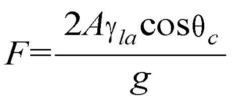
여기서, g는 물기둥의 높이 또는 공간의 두께, γla는 공기 중에서 물의 표면장력, A는 고체와 물의 접촉 면적, 그리고 θc는 고체 표면에서의 물의 접촉각도 이다. 여기서 θc <90도이므로 모세관 힘은 + 값, 즉 인력(attractive force)으로 작용한다. 이 모세관 인력이 미세기전 구조물을 변형시키는데 필요한 힘, 즉 탄성계수 보다 크게 되면, 미세기전 구조물(31a,31b)은 기판(11)쪽으로 휘어져서 일시적으로 점착되게 된다. 그 후 액상의 물이 모두 증발되어도 기판(11)과 미세기전 구조물(31a,31b) 사이의 공간(g)이 없어져서 둘 사이에 작용하는 반 데르 발스의 힘(van der Waals force)에 의해 영구적으로 점착되게 된다. Where g is the height of the water column or the thickness of the space, γ la is the surface tension of water in the air, A is the contact area between the solid and the water, and θ c is the contact angle of the water at the solid surface. Since θ c <90 degrees, the capillary force acts as a positive value, that is, an attractive force. When the capillary attraction becomes larger than the force required to deform the micromechanical structure, that is, the elastic modulus, the
전술한 바와 같이, 기판 및 미세기전 구조물 표면에 잔류하는 액상의 물은 미세기전 구조물이 기판 등의 하부 구조물에 점착되는 문제를 야기시킨다[참조문헌; Offenberg et al., “Vapor HF etching for sacrificial oxide removal in surface micromaching”, Electrochemical Soc. Fall Meet., vol. 94, no. 2, pp. 1056-1057, Oct. 1994, Lee et al., “Dry release for surface micromachining with HF vapor-phase etching”, J. MEMS, vol. 6, no. 3, Sep. 1997.]. 액체 상태의 물 형성을 억제하기 위해서는 기판 온도를 증가시키고, 반응 압력을 감소시켜 야 하는데 이는 산화규소의 식각 속도를 급격히 감소시켜 결과적으로 생산성을 크게 저하시키는 문제를 초래한다.As described above, the liquid water remaining on the substrate and the micromechanical structure surface causes a problem that the micromechanical structure adheres to underlying structures such as the substrate [Reference; Offenberg et al., “Vapor HF etching for sacrificial oxide removal in surface micromaching”, Electrochemical Soc. Fall Meet., Vol. 94, no. 2, pp. 1056-1057, Oct. 1994, Lee et al., “Dry release for surface micromachining with HF vapor-phase etching”, J. MEMS, vol. 6, no. 3, Sep. 1997.]. In order to suppress the formation of water in the liquid state, it is necessary to increase the substrate temperature and to decrease the reaction pressure, which causes a problem of drastically reducing the etching rate of silicon oxide and consequently greatly reducing productivity.
본 발명의 상술한 문제점을 해결하기 위하여 안출된 것으로서, 본 발명의 목적은 미세기전 소자 제조시 희생층을 불산 식각 공정으로 제거할 때 잔류하는 물에 의해 미세기전 구조물이 점착되는 문제를 해결하기 위한 것이다.In order to solve the above problems of the present invention, an object of the present invention is to solve the problem that the micromechanical structure is adhered by the remaining water when the sacrificial layer is removed by the hydrofluoric acid etching process in manufacturing the micromechanical device. will be.
본 발명의 다른 목적은 하부구조물과의 공간 두께(g)가 얇고, 탄성계수가 작은 미세기전 소자를 높은 생산성을 갖도록 제조하는 것이다.
Another object of the present invention is to manufacture a micromechanical device having a low thickness and a small modulus of elasticity with a substructure to have high productivity.
상술한 목적을 달성하기 위한 기술적 수단으로서, 본 발명의 일측면은 희생층의 제거를 통해 부양되는 미세기전 구조물에 관한 것으로서, 상기 미세기전 구조물은 상부 표면을 갖는 하부 구조물; 상기 하부 구조물의 상기 상부 표면의 일영역에 고정되는 일측부; 및 상기 일측부와 연결되며 상기 희생층의 제거를 통해 상기 상부 표면과 대향하는 대향 표면을 갖고 부양되는 타측부를 구비하되, 상기 상부 표면과 상기 대향 표면의 적어도 하나는, 상기 희생층 제거시 생성된 물이 상기 상부 표면과 상기 대형 표면 사이에서 물기둥을 형성하기 않도록 강한 친수성을 갖는 친수성 재료로 형성되는 것을 특징으로 합니다.
바람직하게, 상기 강한 친수성 재료는 알루미늄, 티타늄, 크롬, 철, 코발트, 산화알루미늄, 산화크롬, 산화철, 산화코발트 중 어느 하나이다. 상기 강한 친수성 재료는 상기 상부 표면 및 상기 대향 표면과 상기 희생층 제거시 생성된 물의 접촉 각도가 5 ~23도 범위이다.As a technical means for achieving the above object, one side of the present invention relates to a micromechanical structure that is supported by the removal of the sacrificial layer, the micromechanical structure has a lower structure having an upper surface; A side portion fixed to a region of the upper surface of the lower structure; And the other side connected to the one side and having an opposing surface facing the upper surface through the removal of the sacrificial layer, wherein at least one of the upper surface and the opposing surface is generated when the sacrificial layer is removed. Characterized in that the water is formed of a hydrophilic material having a strong hydrophilic property so as not to form a water column between the upper surface and the large surface.
Preferably, the strong hydrophilic material is any one of aluminum, titanium, chromium, iron, cobalt, aluminum oxide, chromium oxide, iron oxide, cobalt oxide. The strong hydrophilic material has a contact angle between the top surface and the opposing surface and water generated upon removal of the sacrificial layer in the range of 5 to 23 degrees.
바람직하게는, 상부 표면은 상기 하부 구조물에 추가로 형성된 친수성층의 표면일 수 있고, 상기 대향 표면은 추가로 형성된 친수성층의 표면일 수 있다. Preferably, the upper surface may be the surface of a hydrophilic layer further formed in the lower structure, and the opposing surface may be the surface of the further formed hydrophilic layer.
상기 상부 표면과 상기 대향 표면은 서로 같거나 다른 물질로 구성될 수 있다. The upper surface and the opposing surface may be composed of the same or different materials.
상기 친수성층은 예컨대 희생층이 산화규소 희생층인 경우 불산 기체에 의해 식각되지 않는 특성을 갖는 것이 바람직하고, 상기 친수성층은 알루미늄, 티타늄, 산화알루미늄 크롬, 철, 코발트, 산화크롬, 산화철, 산화코발트 중 하나인 것이 바람직하다.Preferably, the hydrophilic layer has a property of not being etched by hydrofluoric acid when the sacrificial layer is a silicon oxide sacrificial layer, and the hydrophilic layer is aluminum, titanium, aluminum chromium oxide, iron, cobalt, chromium oxide, iron oxide, or oxide. It is preferred that it is one of cobalt.
본 발명의 제2 측면은 상부 표면을 갖는 하부 구조물을 형성하는 단계; 상기 하부구조물 상의 소정 영역에 희생층을 형성하는 단계; 상기 하부 구조물의 상기 상부 표면의 일영역에 고정되는 일측부와, 상기 일측부와 연결되며 희생층의 제거를 통해 상기 상부 표면과 대향하는 대향 표면을 갖고 부양되는 타측부를 형성하는 단계; 및 상기 희생층을 제거하여 상기 타측부를 부양시키는 단계를 포함하되, 상기 희생층을 제거할 때, 상기 희생층 제거시 생성된 물이 상기 상부 표면과 상기 대향 표면 사이에서 물기둥을 형성하지 않도록 강한 친수성을 갖는 친수성 재료로 형성되는 것을 특징으로 하는 미세기전 구조물의 제조방법을 제공한다.A second aspect of the invention includes forming a lower structure having an upper surface; Forming a sacrificial layer in a predetermined region on the substructure; Forming one side portion fixed to one region of the upper surface of the lower structure, and the other side portion having an opposing surface connected to the one side and facing the upper surface through removal of the sacrificial layer; And removing the sacrificial layer to support the other side, wherein when the sacrificial layer is removed, the water generated when the sacrificial layer is removed does not form a water column between the upper surface and the opposite surface. It provides a method for producing a micromechanical structure, characterized in that formed from a hydrophilic material having hydrophilicity.
상기 희생층의 식각은 불산(HF) 반응가스와 알코올류(CH3OH, C2H5OH 등) 촉매가스, 그리고 촉매가스를 운반하는 가스(N2, Ar 등)를 포함하는 혼합가스를 사용하여 25-45 ℃의 온도에서 수행하는 것이 바람직하다.The sacrificial layer may be etched using a mixed gas including a hydrofluoric acid (HF) reaction gas, an alcohol (CH 3 OH, C 2 H 5 OH, etc.) catalyst gas, and a gas (N 2 , Ar, etc.) carrying the catalyst gas. It is preferably carried out at a temperature of 25-45 ° C.
본 발명의 제3 측면은 희생층의 제거를 통하여 부양된 미세기전 구조물에 있어서, 상부 표면을 갖는 하부 구조물; 상기 하부 구조물의 상기 상부 표면의 일영역에 고정되는 일측부; 및 상기 희생층의 제거를 통해 상기 상부 표면과 대향하는 대향 표면을 갖고 부양되는 타측부를 구비하되, 상기 상부 표면과 상기 대향 표면 중 적어도 하나의 일영역에는 알루미늄, 티타늄, 크롬, 철, 코발트, 산화알루미늄, 산화크롬, 산화철, 산화코발트 중 어느 하나의 원소로 이루어진 친수성층을 더 포함되는 것을 특징으로 하는 미세기전 구조물을 제공한다.According to a third aspect of the present invention, there is provided a micromechanical structure supported by removal of a sacrificial layer, comprising: a lower structure having an upper surface; A side portion fixed to a region of the upper surface of the lower structure; And the other side having a facing surface facing the upper surface through the removal of the sacrificial layer, wherein at least one region of the upper surface and the facing surface has aluminum, titanium, chromium, iron, cobalt, It provides a micromechanical structure further comprises a hydrophilic layer made of any one of aluminum oxide, chromium oxide, iron oxide, cobalt oxide.
이하, 도 2a 내지 도 2c를 참조하여 본 발명의 바람직한 실시예에 따른 미세기전 구조물을 상세히 설명한다. 도 2a 내지 도 2c는 본 발명의 실시예에 따른 미세 기전 구조물을 설명하기 위한 개념도이다.Hereinafter, the micromechanical structure according to the preferred embodiment of the present invention will be described in detail with reference to FIGS. 2A to 2C. 2A to 2C are conceptual views illustrating the micromechanical structure according to the embodiment of the present invention.
본 미세기전 구조물(31a,31b)은 희생층의 제거를 통하여 부양되는 미세기전 구조물로서, 상부에 표면을 갖는 하부 구조물(11)의 상부 표면에 일측부(31b)가 고정되고, 희생층의 제거를 통해 타측부(31a)가 부양하는 형태로 구성된다. 이 때, 하부 구조물(11)의 상부 표면과 이에 대향하는 미세기전 구조물(31a,31b)의 대향 표면은 희생층 제거시 생성된 물이 면들을 서로 연결하는 물기둥이 생성되지 않도록 하는 강한 친수성 표면으로 구성된다. The
하부 구조물(11)의 친수성 표면은 하부 구조물 자체의 표면 일수도 있고, 하부 구조물(11) 상에 추가로 형성된 제1 친수성층(41)의 표면일 수도 있다. 마찬가지로, 미세기전 구조물(31a,31b)의 친수성 표면도 그 자체의 표면일 수도 있고, 추가로 형성된 제2 친수성층(42)의 표면일 수 있다. 한편, 상부 표면과 대향 표면은 서로 같거나 다른 물질의 친수성 표면으로 구성될 수 있다. 바람직하게는, 추가로 형성된 친수성층은 두께가 5-100 nm인 알루미늄, 티타늄, 크롬, 철, 코발트, 산화알루미늄, 산화크롬, 산화철 또는 산화코발트 박막 형태로 형성된다. 이 경우, 예를 들어 하부구조물(11)이 알루미늄 등으로 이루어진 경우이면 하부구조물(11) 자체가 친수성 표면을 갖는 것이 된다. The hydrophilic surface of the
한편, 도 2a 내지 도 2c에는 하부 구조물(11)의 제1 친수성층(41)과 미세기전 구조물(31a,31b)의 친수성층(42)이 모두 추가적으로 형성한 경우를 예로 도시하고 있지만, 반드시 이에 한정되지 않음은 전술한 바와 같다. 또한 도 3에는 하부 구조물(11)의 상부에 친수성층(41)만이 추가적으로 형성된 구조를 예시하고 있다. 2A to 2C illustrate an example in which both the first
한편, 본 발명에 의하면, 희생층(22)을 제거하는 공정에서 응축된 액상의 물이 상기 강한 친수성 표면층 위에서 적절히 작은 접촉각도를 갖는 넓고 낮은 섬 형태(24)로 형성되어 물 기둥이 형성되지 않도록 한다. 따라서, 하부구조물(11)과 미세기전 구조물(31a,31b) 사이에 모세관 힘이 작용하지 않고, 액상의 물이 증발하여도 미세기전 구조물(31a,31b)은 하부구조물(11)로부터 일정한 간격(g)을 계속 유지하게 되어 점착 현상은 근본적으로 발생하지 않는다. On the other hand, according to the present invention, the liquid water condensed in the process of removing the
즉, 상기 수학식 1에서 전술한 바와 같이, θc <90도이므로 모세관 힘은 + 값, 즉 인력(repulsive force)으로 작용하게 되는데 본 발명에 의하면, 원천적으로 물기둥이 생성되지 않도록 하여 미세기전 구조물(31a,31b)의 점착현상을 방지할 수 있다.That is, as described above in Equation 1, since θ c <90 degrees, the capillary force acts as a positive value, that is, a repulsive force. According to the present invention, the micromechanical structure is prevented from generating water columns inherently. Adhesion of (31a, 31b) can be prevented.
한편, 하부 구조물(11)의 표면과 미세기전 구조물(31a,31b)의 대향 표면에 형성된 액상의 물의 θc 가 90도 초과의 접촉 각도를 갖도록 하는 경우 수학식 1에 의해 인력의 발생을 막을 수 있다. 즉, 하부구조물의 표면과 미세기전 구조물(31a,31b)을 연결하는 물기둥에 의해 작용하는 모세관 힘은 - 값, 즉 척력(repulsive force)으로 작용한다. 그 결과, 액상의 물이 증발하여도 미세기전 구조물(31a,31b)은 하부구조물(11)로부터 일정한 공간을 계속 유지하게 되며, 미세기전 구조물은 정상적으로 부유할 수 있게 된다.On the other hand, θ c of the liquid water formed on the surface of the
그러나, 이러한 물의 접촉각도를 유지하기 위해서는 하부 구조물의 표면과 미세기전 구조물의 대향 표면을 친수성이 아닌 소수성 재료로 형성하여야 한다. 일반적인 소수성 재료로는 self-assembled monolayer (SAM), fluorocarbon (FC) 등과 같은 폴리머(polymer) 재료가 있다. 그러나, 이와 같은 재료들은 다른 재료와의 접착력이 좋지 않고, 열적 안정성이 낮으며, 산화 분위기에서 소수성 특성이 저하되는 문제점들 때문에 미세기전 소자 제조시 실제적으로 사용하기가 어려운 문제점이 있다. 일반적으로 미세기전 소자에서 기판 및 미세기전 구조물로 사용하는 거의 모든 재료, 즉 규소(Si), 질화규소(Si3N4), 금(Au), 알루미늄(Al) 등은 친수성 재료이다.However, in order to maintain such a contact angle of water, the surface of the lower structure and the opposing surface of the micromechanical structure should be formed of hydrophobic material rather than hydrophilic. Typical hydrophobic materials include polymer materials such as self-assembled monolayer (SAM) and fluorocarbon (FC). However, such materials have problems of poor adhesion to other materials, low thermal stability, and difficulty in practical use in manufacturing a microvoltaic device due to problems of deterioration of hydrophobic properties in an oxidizing atmosphere. In general, almost all materials used as substrates and micromechanical structures in micromechanical devices, that is, silicon (Si), silicon nitride (Si 3 N 4 ), gold (Au), aluminum (Al), and the like are hydrophilic materials.
산화규소 증착후 불산 기상식각 공정으로 제거한 경우 측정된 친수성을 갖는 물질들의 접촉각도를 살펴보면, 알루미늄은 물의 접촉각도가 17도, 티타늄은 8도, 크롬은 23도, 산화알루미늄은 5도로 매우 강한 친수성을 갖고 있다.When the contact angles of the hydrophilic materials measured after removal of silicon oxide were removed by hydrofluoric acid vapor etching process, the contact angle of aluminum is 17 degrees, aluminum is 8 degrees, chromium is 23 degrees, and aluminum oxide is 5 degrees. Have
바람직하게는, 상기 희생층은 산화규소로 이용한다. 예를 들어 산화규소(thermal oxide, thermal CVD oxide, PECVD oxide, SOG, sputtered oxide, evaporated oxide 등), 인(P)이 첨가된 산화규소(PSG), 그리고 붕소(B)와 인(P)이 첨가된 산화규소(BPSG)를 채용할 수 있다. Preferably, the sacrificial layer is used as silicon oxide. For example, silicon oxide (thermal oxide, thermal CVD oxide, PECVD oxide, SOG, sputtered oxide, evaporated oxide, etc.), phosphorus (P) added silicon oxide (PSG), and boron (B) and phosphorus (P) Added silicon oxide (BPSG) can be employed.
제거되는 희생층을 산화규소로 이용하는 경우 불산 기상식각 공정은 불산(HF) 반응가스와 알코올류(CH3OH, C2H5OH 등) 촉매가스, 그리고 촉매가스를 운반하는 가스(N2, Ar 등)를 포함하는 혼합가스를 사용하여 25-45 ℃의 온도에서 진행한다. 이 경우, 규소(Si), 금(Au), 등의 친수성 재료는 불산 기체에 의해 화학적으로 식각되지 않으며, 산화규소 증착후 불산 기상식각 공정으로 제거한 경우 측정된 물의 접촉각도는 대략 50~80도 사이이다. 이와 같은 물의 접촉각도는 하부 구조물의 표면과 미세기전 구조물의 대향 표면을 접착시키는 조건을 만족할 가능성이 있다. In the case of using the removed sacrificial layer as silicon oxide, the hydrofluoric acid gas phase etching process includes a hydrofluoric acid (HF) reaction gas, alcohols (CH 3 OH, C 2 H 5 OH, etc.), a catalyst gas, and a gas (N 2 , Proceed at a temperature of 25-45 ° C. using a mixed gas containing Ar or the like). In this case, hydrophilic materials such as silicon (Si), gold (Au), and the like are not chemically etched by hydrofluoric acid gas, and the contact angle of water measured when silicon oxide is removed by the hydrofluoric acid vapor deposition process is approximately 50 to 80 degrees. Between. Such a contact angle of water is likely to satisfy the conditions for bonding the surface of the lower structure and the opposing surface of the micromechanical structure.
이하, 상기 미세기전 구조물이 적용가능한 소자 중 미세기전 스위치를 예로 들어 상세히 설명한다. 도 4a 및 도 4b는 본 발명의 바람직한 실시예에 따른 미세기전 스위치의 단면도와 평면도이다. 본 미세기전 스위치는 정전기력(electrostatic force)으로 구동되는 저항식(resistive) 고주파(radio frequency, RF) 미세기전 스위치이다. Hereinafter, a micromechanical switch among the devices to which the micromechanical structure is applicable will be described in detail. 4A and 4B are a cross-sectional view and a plan view of a micromechanical switch according to a preferred embodiment of the present invention. The micromechanical switch is a resistive radio frequency (RF) micromechanical switch driven by electrostatic force.
미세 기전 스위치는 기판(111) 위에 형성되는 입력단과 출력단이 분리된 형 태의 신호선(112), 신호선(112)의 양쪽에 형성되는 접지선(113), 접지선 중 하나로 형성되는 하부전극(114), 바이어스 전극(115)과 바이어스 전극(115) 위에 형성되는 포스트(121)와 이를 둘러싸고 있는 산화규소 희생층(미도시)과 포스트(121)에 의해 한쪽 끝이 기판(111)에 고정되며 신호선(113) 및 하부전극(114)으로부터 일정한 두께의 산화규소 희생층(미도시)을 두고 형성되는 외팔보 형태의 이동판(132)과, 그 위에 하부전극(114)과 대칭되도록 형성되는 상부전극(133)과, 이동판(132)의 고정되지 않은 끝에 신호선(112)의 개방부(open gap)와 대칭되도록 형성되는 접촉패드(134)으로 구성된다. The micro electromechanical switch includes a
한편, 예컨대 금으로 형성된 하부전극(113)의 윗면의 적어도 일부에 알루미늄(Al) 또는 티타늄(Ti)의 제1 친수성층(141)이 형성되고, 규소로 형성된 이동판(132)의 밑면에는 산화알루미늄(Al2O3)의 제2 친수성층(142)이 형성된다. 알루미늄과 티타늄은 모두 하부전극(113)인 금과 같이 전도성을 갖는 금속 재료이고, 산화알루미늄은 규소와 같이 절연성이 우수한 재료이므로 상기 친수성층 형성이 스위치의 동작특성에는 별다른 영향을 미치지 않는다. Meanwhile, for example, a first
제1 친수성층(141)과 제2 친수성층(142)은 산화규소 희생층을 불산 식각공정으로 식각할 때 생성된 물이 제1 친수성 층(141)과 제2 친수성층(142)을 서로 연결하는 물기둥으로 되지 않도록 하는 기능을 수행한다.
다음으로, 이와 같은 구조를 갖는 정전구동형 저항식 고주파 미세기전 스위치의 동작원리를 살펴보면 다음과 같다. 먼저, 바이어스 전극(115)에 일정한 전압을 인가하면 바이어스 전극(115)과 전기적으로 연결된 상부전극(133)과 접지 상태의 하부전극(114) 사이에 정전기력이 발생하고, 이 정전기력에 의해 상부전극(133)과 이동판(132)이 기판(111)쪽으로 휘어지게 되며, 그 결과 접촉패드(134)가 분리된 신호선(112)의 입력단 및 출력단과 동시에 접촉하여 서로 연결시켜 줌으로써 신호는 전달된다. In the first
Next, the operation principle of the electrostatically driven resistance type high frequency micromechanical switch having such a structure is as follows. First, when a constant voltage is applied to the
삭제delete
이때, 스위치의 응용 가능성을 높이기 위해서 낮은 구동전압이 요구되므로 하부전극(114)와 상부전극(133) 사이의 간격을 작게 하는 것이 중요하다. 반면, 바이어스 전극(115)에 인가한 전압을 차단하면, 휘어져있던 이동판(132)과 상부전극(133)이 탄성복원력(elastic restoring force)에 의해 펴지게 되고, 그 결과 접촉패드(134)가 신호선(112)으로부터 탈착되어 신호는 차단된다. In this case, since a low driving voltage is required in order to increase the applicability of the switch, it is important to reduce the distance between the
한편, 정전구동형 저항식 고주파 미세기전 스위치 제조시 일반적으로 사용하는 재료는 다음과 같다. 기판(11)은 절연성 갈륨비소(semi-insulating GaAs)로, 신호선(12)과 접지선(13) 및 접촉패드(34)는 전도성(electrical conduction)이 우수한 금(Au)으로, 그리고 이동판(32)은 불산 기상식각 공정시 화학적으로 안정하며 우수한 절연성(electrical insulation)을 갖는 불순물이 첨가 되지 않은 규소(undoped-silicon, Si)로 형성한다. 그리고, 바이어스 전극(15), 포스트(21)와 상부 전극(33)은 전도성(conducting) 금속 재료로 형성한다.On the other hand, materials commonly used in the manufacture of electrostatically driven resistive high frequency micromechanical switches are as follows. The
다음으로, 도 5a 내지 도 5i를 참조하여 본 발명의 바람직한 실시예에 따른 미세기전 스위치의 제작과정의 일예를 상세히 설명한다.Next, an example of the manufacturing process of the micromechanical switch according to the preferred embodiment of the present invention will be described in detail with reference to FIGS. 5A to 5I.
도 5a 및 도 5b를 참조하면, GaAs 기판(111) 상에 PECVD(Plasma Enhanced Chemical Vapor Deposition), RF(Radio Frequency) 스퍼터링(sputtering), 전자빔 증착(e-beam evaporation) 등의 공정을 사용하여 산화규소 희생층(122a)을 증착한다. 다음으로, 산화규소 희생층(122a) 상에 네거티브 포토레지스트층(Photo-Resist:123)을 코팅하고, 광 리소그라피 공정을 사용하여 소정의 영역(즉, 신호선, 접지선 및 바이어스 전극 영역)을 규정하는 패터닝한 후, RIE(Reactive Ion Etching)법을 사용하여 산화규소 희생층(123)을 식각하여 기판(111)을 노출시킨다.5A and 5B, oxidation is performed on a
도 5c를 참조하면, 전자빔 증착법(E-beam evaporation법)을 사용하여 Au 전극층(112,113,114,115)을 증착한 후, 리프트 오프(lift-off)법을 사용하여 포토레지스트층(Photo-Resist:123)과 그 위에 형성된 Au 전극층(112,113,114,115)을 동시에 제거함으로써 식각된 산화규소(SiO2) 트랜치 패턴 안에 Au 전극층(112,113,114,115)을 형성한다. 이때, Au 전극층(112,113,114,115)과 GaAs 기판(111) 사이에는 접착력 향상을 위하여 Ti층(미도시)을 형성할 수 있다.Referring to FIG. 5C, after depositing the Au electrode layers 112, 113, 114 and 115 using an electron beam evaporation method, the
도 5d를 참조하면, 포토레지스트층(123)의 코팅 및 패터닝 공정을 접지선113)의 일부 영역(즉, 하부전극(114) 영역)을 규정한 후, Ti (또는 Al, Cr 등) evaporation 및 lift-off 공정을 사용하여 친수성 표면을 갖는 제1 친수성층(141)을 형성한다. Referring to FIG. 5D, after coating and patterning the
도 5e를 참조하면, 기 형성된 산화규소층(122a)에 새로운 산화규소층을 형성하여 산화규소 희생층(122)이 형성되도록 하고, 이어서 포토레지스트 코팅 및 패터닝, 산화규소층의 선택적 식각, Au층 증착과 리프트 공정을 사용하여 포스트(121)를 형성한다. Referring to FIG. 5E, a new silicon oxide layer is formed on the formed
도 5f를 참조하면, 포토레지스트 코팅 및 패터닝 공정을 사용하여 신호선(112)과 접촉패드(134)가 중첩되는 영역을 규정한 후, 일정한 두께의 산화규소 희생층(122)을 식각하여 홈 형상(H)을 형성한다. Referring to FIG. 5F, after defining a region where the
도 5g를 참조하면, 포토레지스트 코팅 및 패터닝 공정을 사용하여 소정 영역을 규정한 후, 전자빔 증착(e-beam evaporation) 및 lift-off 공정을 사용하여 강한 친수성을 갖는 Al2O3의 제2 친수성층(142)과 실리콘의 이동판(132)을 형성한다Referring to FIG. 5G, after defining a predetermined region using a photoresist coating and patterning process, a second hydrophilicity of Al 2 O 3 having strong hydrophilicity using an e-beam evaporation and lift-off process The
도 5h를 참조하면, 포토레지스트 코팅 및 패터닝 공정을 사용하여 소정 영역을 규정한 후, 전자빔 증착(e-beam evaporation) 및 lift-off 공정을 사용하여 Au 상부전극(133) 및 접촉패드(134)를 형성한다.Referring to FIG. 5H, after defining a predetermined region using a photoresist coating and patterning process, the Au
도 5i를 참조하면, HF 기상식각 공정을 사용하여 산화규소 희생층(122)을 제거한다. 불산 기상식각 공정은 불산(HF) 반응가스와 알코올류(CH3OH, C2H5OH 등) 촉매가스, 그리고 촉매가스를 운반하는 가스(N2, Ar 등)를 포함하는 혼합가스를 사용하여 25-45 ℃의 온도에서 진행한다. 이때 산화규소 희생층(122)의 제거를 원활하게 하기 위해서 상기 이동판(132)과 Au 상부전극(133)에는 에칭 홀(미도시)을 형성할 수 있는데, 도면에서는 도시하지 않았다.Referring to FIG. 5I, the silicon oxide
(비교예)(Comparative Example)
전술한 미세기전 스위치를 실제 제작하여 미세 구조물의 점착여부를 비교하는 실험을 실시하였다. 도 6 및 도 7은 친수성층을 형성한 미세기전 스위치와 친수성층이 형성되지 않은 미세기전 스위치의 평면 SEM(주사 전자 현미경, Scanning Electron Microscope)사진과 3차원 형상 분석 장비(3D surface profiling system)로 관찰한 결과를 나타내는 도면들이다. 친수성층이 형성된 미세기전 스위치는 상기 도 4를 참조로 설명한 미세기전 스위치와 구조가 동일하다. The micromechanical switch described above was actually manufactured to compare the adhesion of the microstructures. 6 and 7 are planar SEM (Scanning Electron Microscope) photographs of the micromechanical switch in which the hydrophilic layer is formed and the micromechanical switch in which the hydrophilic layer is not formed, and a 3D surface profiling system. The figure which shows the result of observation. The micromechanical switch in which the hydrophilic layer is formed has the same structure as the micromechanical switch described with reference to FIG. 4.
도 4a를 참조하여 구체적인 제작조건을 설명한다. 기판(111)은 절연성 갈륨비소, 신호선(112)과 하부전극(114)은 0.5㎛ 두께의 금 박막, 이동판(132)은 0.3㎛ 두께의 규소 박막, 상부전극(133)은 0.9㎛ 두께의 금 박막으로 형성하였다. 그리고, 산화규소 희생층(122)의 두께는 하부전극(114)과 이동판(132) 사이에서 0.5㎛로 매우 얇게 형성하여, 스위치가 낮은 구동전압을 갖도록 하였다. 그리고, 0.45㎛ 두께의 금 박막으로 형성된 하부전극(114)의 윗면에 0.05㎛ 두께의 알루미늄으로 제1 친수성층(141)을 형성하였으며, 0.25㎛ 두께의 규소 박막으로 형성된 이동판(132)의 밑면에 0.05㎛ 두께의 산화알루미늄으로 제2 친수성층(142)을 형성하였다. A detailed manufacturing condition will be described with reference to FIG. 4A. The
도 6의 하부도면은 상기 미세기전 스위치를 실제로 제작한 후, 불산 기상식각 공정으로 산화규소 희생층을 제거한 상태에서 3차원 형상 분석 장비로 관찰한 결과이다. 하부전극(114)의 표면에서 상부전극(133) 표면까지 높이는 2.0~5.1㎛로 제2 친수성층(142)과 이동판(132), 그리고 상부전극(133)의 삼중층으로 형성된 외 팔보 형태의 미세기전 구조물의 두께 1.2㎛ 보다 크다. 이는 상기 미세기전 구조물이 점착되지 않고 정상적으로 부유되어 있다는 것을 의미한다. 참고로, 상기 미세기전 구조물이 휘어져 있는 것은 잔류응력에 의한 것으로 본 발명의 내용과는 무관한 것이다.6 is a result of actually manufacturing the micromechanical switch and then observing it with a three-dimensional shape analysis device in a state in which the silicon oxide sacrificial layer was removed by a hydrofluoric acid vapor etching process. The height from the surface of the
친수성층이 형성되지 않은 미세기전 스위치는 상술한 친수성층이 형성된 미세기전 스위치에서 제1 및 제2 친수성층을 제외한 구조로 제작되었다. 도 7의 결과를 참조하면, 기판(111) 및 하부전극(114)의 표면에서 상부전극(133) 표면까지 높이는 1.2㎛로 이동판(132)의 두께인 0.3㎛와 상부전극(133)의 두께 0.9㎛의 합과 같다. 이는 이동판(132)과 그 위에 형성된 상부전극(133)의 이중층(bi-layer)으로 형성된 외팔보 형태의 미세기전 구조물이 점착되었다는 것을 의미한다. The micromechanical switch in which the hydrophilic layer was not formed was manufactured in the above-described micromechanical switch except for the first and second hydrophilic layers. Referring to the result of FIG. 7, the height from the surfaces of the
본 발명자들은 미세기전 스위치 점착 현상의 원인을 규명하기 위하여 사용한 구조 재료들에 희생층을 형성한 후 식각 공정으로 제거한 경우 표면에서 물의 접촉각도를 조사하였다. 그 결과, 갈륨비소는 물의 접촉각도가 19도로 강한 친수성을 갖는 반면, 규소와 금은 물의 접촉각도가 각각 57도와 62도로 약한 친수성을 갖는다. 따라서, 불산 기상식각 공정으로 산화물 희생층 제거시 갈륨비소 기판과 규소 이동판 사이, 금 하부전극(114)과 규소 이동판(132) 사이, 그리고 금 신호선(132)과 금 접촉패드(134) 사이에서 물기둥이 형성되기 쉽다. 특히, 상대적으로 간격이 좁고, 면적이 넓은 규소 이동판(132)과 금 하부전극(114) 사이에서 물 기둥 형성이 용이하다. 따라서, 스위치의 점착 현상은 이동판(132)과 금 하부전극(114) 사이에서 생성되는 물 기둥에 의해 작용하는 모세관 인력에 의해 발생한 것이다.The present inventors investigated the contact angle of water on the surface when the sacrificial layer was formed on the structural materials used to identify the cause of the micromechanical switch adhesion phenomenon and then removed by the etching process. As a result, gallium arsenide has a strong hydrophilicity of water contact angle of 19 degrees, while silicon and gold have a weak hydrophilicity of water contact angle of 57 degrees and 62 degrees, respectively. Accordingly, when the oxide sacrificial layer is removed by a hydrofluoric acid vapor etching process, between the gallium arsenide substrate and the silicon transfer plate, between the gold
반면에 알루미늄은 물의 접촉각도가 17도, 티타늄은 8도, 산화알루미늄은 5도로 매우 강한 친수성을 갖고 있다. 또한 상기 재료들은 불산 기상식각 공정 조건하에서 화학적으로 매우 안정하므로 거의 식각되지 않는다. 따라서, 도 6에 도시된 미세기전 스위치는 불산 기상식각 공정에 의한 산화규소 희생층 제거시 산화규소 희생층을 둘러싸고 있는 구조체의 표면들이 모두 강한 친수성이므로 액상의 물 기둥이 형성되지 않으므로 점착 현상이 발생하지 않는다. On the other hand, aluminum has a very strong hydrophilicity, with a contact angle of water of 17 degrees, titanium of 8 degrees, and aluminum oxide of 5 degrees. In addition, the materials are rarely etched because they are chemically very stable under hydrofluoric acid vapor etching process conditions. Therefore, the micromechanical switch shown in FIG. 6 has a strong hydrophilic surface when the silicon oxide sacrificial layer is removed by the hydrofluoric acid vapor etching process, so that the liquid water column is not formed. I never do that.
상술한 바와 같이, 본 발명에 의하면 희생층의 제거를 통하여 부양되는 미세기전 구조물에서, 희생층을 제거하는 단계시 미세기전 구조물이 점착되는 문제를 해결할 수 있으므로 하부구조물과 미세기전 구조물 사이의 간격을 작게 할 수 있어 우수한 특성을 갖는 미세기전 구조물을 높은 수율로 제조할 수 있는 효과가 있다 As described above, according to the present invention, in the micromechanical structure supported by the removal of the sacrificial layer, it is possible to solve the problem that the micromechanical structure is adhered to when the sacrificial layer is removed, thereby reducing the gap between the substructure and the micromechanical structure. It can be made small, there is an effect that can be produced in a high yield of a micromechanical structure having excellent characteristics
Claims (16)
Priority Applications (3)
| Application Number | Priority Date | Filing Date | Title |
|---|---|---|---|
| KR1020040045258A KR100627139B1 (en) | 2004-06-18 | 2004-06-18 | Micromechanical structures and Method thereof |
| PCT/KR2004/003360 WO2005124869A1 (en) | 2004-06-18 | 2004-12-20 | Micro-mechanical structure and method for manufacturing the same |
| US11/596,343 US7728395B2 (en) | 2004-06-18 | 2004-12-20 | Micro-mechanical structure and method for manufacturing the same |
Applications Claiming Priority (1)
| Application Number | Priority Date | Filing Date | Title |
|---|---|---|---|
| KR1020040045258A KR100627139B1 (en) | 2004-06-18 | 2004-06-18 | Micromechanical structures and Method thereof |
Publications (2)
| Publication Number | Publication Date |
|---|---|
| KR20050120066A KR20050120066A (en) | 2005-12-22 |
| KR100627139B1 true KR100627139B1 (en) | 2006-09-25 |
Family
ID=35510009
Family Applications (1)
| Application Number | Title | Priority Date | Filing Date |
|---|---|---|---|
| KR1020040045258A KR100627139B1 (en) | 2004-06-18 | 2004-06-18 | Micromechanical structures and Method thereof |
Country Status (3)
| Country | Link |
|---|---|
| US (1) | US7728395B2 (en) |
| KR (1) | KR100627139B1 (en) |
| WO (1) | WO2005124869A1 (en) |
Families Citing this family (18)
| Publication number | Priority date | Publication date | Assignee | Title |
|---|---|---|---|---|
| US7450295B2 (en) * | 2006-03-02 | 2008-11-11 | Qualcomm Mems Technologies, Inc. | Methods for producing MEMS with protective coatings using multi-component sacrificial layers |
| US7417784B2 (en) | 2006-04-19 | 2008-08-26 | Qualcomm Mems Technologies, Inc. | Microelectromechanical device and method utilizing a porous surface |
| JP2008132583A (en) * | 2006-10-24 | 2008-06-12 | Seiko Epson Corp | Mems device |
| EP2129619A2 (en) | 2007-04-04 | 2009-12-09 | Qualcomm Mems Technologies, Inc. | Eliminate release etch attack by interface modification in sacrificial layers |
| KR100844143B1 (en) * | 2007-05-02 | 2008-07-04 | 재단법인서울대학교산학협력재단 | Method for fabricating for three dimensional structured micro-electrode array |
| US7719752B2 (en) | 2007-05-11 | 2010-05-18 | Qualcomm Mems Technologies, Inc. | MEMS structures, methods of fabricating MEMS components on separate substrates and assembly of same |
| US7738158B2 (en) | 2007-06-29 | 2010-06-15 | Qualcomm Mems Technologies, Inc. | Electromechanical device treatment with water vapor |
| WO2009050209A2 (en) * | 2007-10-15 | 2009-04-23 | Epcos Ag | Manufacturing a mems element having cantilever and cavity on a substrate |
| DE102008001038B4 (en) * | 2008-04-08 | 2016-08-11 | Robert Bosch Gmbh | Micromechanical component with a slanted structure and corresponding manufacturing method |
| US7851239B2 (en) | 2008-06-05 | 2010-12-14 | Qualcomm Mems Technologies, Inc. | Low temperature amorphous silicon sacrificial layer for controlled adhesion in MEMS devices |
| US8389317B2 (en) * | 2009-05-28 | 2013-03-05 | Shanghai Lexvu Opto Microelectronics Technology Co., Ltd. | MEMS device and method of fabricating the same |
| JP5589515B2 (en) | 2010-04-05 | 2014-09-17 | セイコーエプソン株式会社 | Method for manufacturing inclined structure |
| EP2460762B1 (en) * | 2010-12-06 | 2014-10-08 | Nxp B.V. | MEMS device having reduced stiction and manufacturing method |
| US9221677B2 (en) * | 2010-12-20 | 2015-12-29 | Rf Micro Devices, Inc. | Composite sacrificial structure for reliably creating a contact gap in a MEMS switch |
| US8643140B2 (en) * | 2011-07-11 | 2014-02-04 | United Microelectronics Corp. | Suspended beam for use in MEMS device |
| JP5845690B2 (en) * | 2011-07-27 | 2016-01-20 | セイコーエプソン株式会社 | Tilting structure, manufacturing method of tilting structure, and spectroscopic sensor |
| JP5803419B2 (en) * | 2011-08-19 | 2015-11-04 | セイコーエプソン株式会社 | Tilting structure, manufacturing method of tilting structure, and spectroscopic sensor |
| DE102019126351A1 (en) * | 2019-09-30 | 2021-04-01 | Tdk Electronics Ag | Switching device |
Family Cites Families (10)
| Publication number | Priority date | Publication date | Assignee | Title |
|---|---|---|---|---|
| US5658698A (en) * | 1994-01-31 | 1997-08-19 | Canon Kabushiki Kaisha | Microstructure, process for manufacturing thereof and devices incorporating the same |
| KR100237000B1 (en) | 1996-09-21 | 2000-01-15 | 정선종 | Method for fabricating microstructures by using sacrifical oxide |
| US20020155299A1 (en) * | 1997-03-14 | 2002-10-24 | Harris Caroline S. | Photo-induced hydrophilic article and method of making same |
| US6238580B1 (en) | 1998-02-20 | 2001-05-29 | The Aerospace Corporation | Method of HF vapor release of microstructures |
| US6372700B1 (en) * | 2000-03-31 | 2002-04-16 | 3M Innovative Properties Company | Fluorinated solvent compositions containing ozone |
| US6488228B2 (en) * | 2000-09-22 | 2002-12-03 | 3M Innovative Properties Company | Tape for flying splice, method of use, and method of manufacture |
| KR100381011B1 (en) * | 2000-11-13 | 2003-04-26 | 한국전자통신연구원 | Stiction-free release method of microstructure for fabrication of MEMS device |
| JP3770158B2 (en) * | 2001-12-26 | 2006-04-26 | ソニー株式会社 | Manufacturing method of MEMS element |
| JP3755460B2 (en) | 2001-12-26 | 2006-03-15 | ソニー株式会社 | Electrostatically driven MEMS element and manufacturing method thereof, optical MEMS element, light modulation element, GLV device, laser display, and MEMS apparatus |
| JP3558066B2 (en) * | 2002-02-19 | 2004-08-25 | ソニー株式会社 | MEMS element and its manufacturing method, light modulation element, GLV device and its manufacturing method, and laser display |
-
2004
- 2004-06-18 KR KR1020040045258A patent/KR100627139B1/en not_active IP Right Cessation
- 2004-12-20 US US11/596,343 patent/US7728395B2/en not_active Expired - Fee Related
- 2004-12-20 WO PCT/KR2004/003360 patent/WO2005124869A1/en active Application Filing
Also Published As
| Publication number | Publication date |
|---|---|
| KR20050120066A (en) | 2005-12-22 |
| WO2005124869A1 (en) | 2005-12-29 |
| US7728395B2 (en) | 2010-06-01 |
| US20070215965A1 (en) | 2007-09-20 |
Similar Documents
| Publication | Publication Date | Title |
|---|---|---|
| KR100627139B1 (en) | Micromechanical structures and Method thereof | |
| EP0683921B1 (en) | Microstructures and single mask, single-crystal process for fabrication thereof | |
| US5426070A (en) | Microstructures and high temperature isolation process for fabrication thereof | |
| Albrecht et al. | Microfabrication of cantilever styli for the atomic force microscope | |
| US7053737B2 (en) | Stress bimorph MEMS switches and methods of making same | |
| US6108121A (en) | Micromachined high reflectance deformable mirror | |
| US6882264B2 (en) | Electrothermal self-latching MEMS switch and method | |
| US7152300B1 (en) | Method of manufacturing a micromechanical structure | |
| US20090014296A1 (en) | Contact configurations for MEMS relays and MEMS switches and method for making same | |
| de Boer et al. | The black silicon method V: A study of the fabricating of movable structures for micro electromechanical systems | |
| US20080011066A1 (en) | Atomic force microscope cantilever and method for manufacturing the same | |
| CN102375332B (en) | Suspension photoresist planarization technology for MEMS structure | |
| CN112897457A (en) | Semiconductor device and method for manufacturing the same | |
| EP1532637B1 (en) | Method of forming atomic force microscope tips | |
| JP4994096B2 (en) | Semiconductor device manufacturing method and semiconductor device using the same | |
| US7041611B2 (en) | Enhancement of fabrication yields of nanomechanical devices by thin film deposition | |
| CN214829017U (en) | Semiconductor device with a plurality of transistors | |
| Chrusch et al. | Corrugated micromachined membrane structures | |
| Chandra et al. | Design and development of microstructures for MEMS applications | |
| Yang et al. | A new surface modification method to prevent the release-stiction of micromechanical structures during HF vapor-phase etching | |
| CN112340695A (en) | Polysilicon cantilever beam array structure and preparation method and application thereof | |
| KR100701151B1 (en) | Method of fabricating air-gap structure for microelectromechanical system | |
| Pham et al. | Polyimide sacrificial layer for an all-dry post-process surface micromachining module | |
| Boucinha et al. | Application of Thin-Film Micromachining for Large-Area Substrates | |
| WO2023094673A1 (en) | Fabrication method for a thin-film layer on a substrate |
Legal Events
| Date | Code | Title | Description |
|---|---|---|---|
| A201 | Request for examination | ||
| E902 | Notification of reason for refusal | ||
| E902 | Notification of reason for refusal | ||
| E701 | Decision to grant or registration of patent right | ||
| GRNT | Written decision to grant | ||
| FPAY | Annual fee payment |
Payment date: 20100901 Year of fee payment: 5 |
|
| LAPS | Lapse due to unpaid annual fee |