KR100240367B1 - Ic card - Google Patents
Ic card Download PDFInfo
- Publication number
- KR100240367B1 KR100240367B1 KR1019970008037A KR19970008037A KR100240367B1 KR 100240367 B1 KR100240367 B1 KR 100240367B1 KR 1019970008037 A KR1019970008037 A KR 1019970008037A KR 19970008037 A KR19970008037 A KR 19970008037A KR 100240367 B1 KR100240367 B1 KR 100240367B1
- Authority
- KR
- South Korea
- Prior art keywords
- panel
- card
- frame
- edge
- width direction
- Prior art date
Links
Images


Classifications
-
- H—ELECTRICITY
- H05—ELECTRIC TECHNIQUES NOT OTHERWISE PROVIDED FOR
- H05K—PRINTED CIRCUITS; CASINGS OR CONSTRUCTIONAL DETAILS OF ELECTRIC APPARATUS; MANUFACTURE OF ASSEMBLAGES OF ELECTRICAL COMPONENTS
- H05K5/00—Casings, cabinets or drawers for electric apparatus
- H05K5/02—Details
- H05K5/0256—Details of interchangeable modules or receptacles therefor, e.g. cartridge mechanisms
- H05K5/026—Details of interchangeable modules or receptacles therefor, e.g. cartridge mechanisms having standardized interfaces
- H05K5/0265—Details of interchangeable modules or receptacles therefor, e.g. cartridge mechanisms having standardized interfaces of PCMCIA type
- H05K5/0269—Card housings therefor, e.g. covers, frames, PCB
-
- B—PERFORMING OPERATIONS; TRANSPORTING
- B42—BOOKBINDING; ALBUMS; FILES; SPECIAL PRINTED MATTER
- B42D—BOOKS; BOOK COVERS; LOOSE LEAVES; PRINTED MATTER CHARACTERISED BY IDENTIFICATION OR SECURITY FEATURES; PRINTED MATTER OF SPECIAL FORMAT OR STYLE NOT OTHERWISE PROVIDED FOR; DEVICES FOR USE THEREWITH AND NOT OTHERWISE PROVIDED FOR; MOVABLE-STRIP WRITING OR READING APPARATUS
- B42D25/00—Information-bearing cards or sheet-like structures characterised by identification or security features; Manufacture thereof
- B42D25/40—Manufacture
-
- G—PHYSICS
- G06—COMPUTING; CALCULATING OR COUNTING
- G06K—GRAPHICAL DATA READING; PRESENTATION OF DATA; RECORD CARRIERS; HANDLING RECORD CARRIERS
- G06K19/00—Record carriers for use with machines and with at least a part designed to carry digital markings
- G06K19/06—Record carriers for use with machines and with at least a part designed to carry digital markings characterised by the kind of the digital marking, e.g. shape, nature, code
- G06K19/067—Record carriers with conductive marks, printed circuits or semiconductor circuit elements, e.g. credit or identity cards also with resonating or responding marks without active components
- G06K19/07—Record carriers with conductive marks, printed circuits or semiconductor circuit elements, e.g. credit or identity cards also with resonating or responding marks without active components with integrated circuit chips
- G06K19/077—Constructional details, e.g. mounting of circuits in the carrier
-
- Y—GENERAL TAGGING OF NEW TECHNOLOGICAL DEVELOPMENTS; GENERAL TAGGING OF CROSS-SECTIONAL TECHNOLOGIES SPANNING OVER SEVERAL SECTIONS OF THE IPC; TECHNICAL SUBJECTS COVERED BY FORMER USPC CROSS-REFERENCE ART COLLECTIONS [XRACs] AND DIGESTS
- Y10—TECHNICAL SUBJECTS COVERED BY FORMER USPC
- Y10S—TECHNICAL SUBJECTS COVERED BY FORMER USPC CROSS-REFERENCE ART COLLECTIONS [XRACs] AND DIGESTS
- Y10S439/00—Electrical connectors
- Y10S439/946—Memory card cartridge
Abstract
본 발명은 상부표면과 하부표면이 각각 패널로 덮여지고 있는 IC 카드의 구조 및 제조 방법을 제공하는데 있다.The present invention provides a structure and a manufacturing method of an IC card in which an upper surface and a lower surface are respectively covered with a panel.
IC 카드(1)에 있어서 그 상부표면과 좌우의 측면이 제 1 패널(6c)에 의해 덮여지고, 그 하부표면이 제 2 패널(6d)에 의해서 덮여지고 있다. 여기서, 제 1 패널(6c)은 좌우의 양 단면부 영역의 각각을, 테두리체(5)의 측(side)테두리체(5b)의 외면에 대응하여 2회 절곡한 후에 그 훅크부(16)(앞단부)를 측테두리체(5b)의 하부표면에 계합하므로써 접착지를 사용하지 않고도 테두리체(5)에 직접 취부되어, 상기 IC 카드의 구조 및 그 제조 방법이 간소화된다.In the IC card 1, the upper surface and left and right side surfaces thereof are covered by the first panel 6c, and the lower surface thereof is covered by the second panel 6d. Here, the first panel 6c has bent the hook portion 16 after bending each of the left and right cross-sectional area of the left and right two times corresponding to the outer surface of the side border 5b of the frame 5. By engaging (front end) with the lower surface of the side border body 5b, it is directly attached to the frame 5 without using adhesive paper, thereby simplifying the structure of the IC card and its manufacturing method.
Description
본 발명은 IC 카드에 관한 것으로, 특히 IC 카드의 구조 간소화 및 그 제조 방법의 간략화 등을 꾀하기위한 기술에 관한 것이다.BACKGROUND OF THE
IC(집적회로)를 포함하고 있는 전자부품 등이 카드 형태(얇은 판자 형태)의 케이스내에 내장되는 IC 카드는 종래부터 알려져 있지만, 이러한 종래의 IC 카드의 일례를 도 34∼도 36에 도시하고 있다. 여기서, 도 34는 상기 IC 카드의 전체 사시도이다. 또한, 도 35는 도 34의 F-F 선 단면을 도시하는 단면도이고, 도 36은 상기 IC 카드의 내부구성을 도시하는 분해 사시도이다.IC cards in which electronic parts and the like containing ICs (integrated circuits) are incorporated in a card-like (thin board-like) case have been known in the past, but examples of such conventional IC cards are shown in FIGS. 34 to 36. . 34 is an overall perspective view of the IC card. 35 is a cross-sectional view showing a cross section taken along the line F-F in FIG. 34, and FIG. 36 is an exploded perspective view showing the internal structure of the IC card.
도 34∼도 36에 있어서, (1)은 IC 카드이고, (2)는 IC를 포함하고 있는 전자부품이고, (3)은 전자부품(2)을 탑재하고 있는 기판이다. 또한, (4)는 상기 기판(3)에 접속되는 한편 시스템기기(도시하지 않음)와의 신호의 수수를 행하는 커넥터(connector)이고, (5)는 상기 커넥터(4)와 전자부품(2)을 탑재하고 있는 기판(3)을 격납·유지하는 수지제의 테두리체(frame)이고, (6a) 및 (6b)는 각기 테두리체(5)에 접착·고정되어 상기 커넥터(4) 및 전자부품(2)을 탑재하고 있는 기판(3)을 표리(表裏)양면에서 덮는 금속제의 제 1 패널(전면 패널) 및 제 2 패널(후면 패널)이다. (7a) 및 (7b)는 각기 상기테두리체(5)와 각 패널(6a), (6b)를 접착·고정하는 접착지이다.34 to 36, (1) is an IC card, (2) is an electronic component containing an IC, and (3) is a substrate on which the
그러나, 이러한 종래의 IC 카드는 비교적 가격이 비싸다고 하는 문제가 있었다. 이것 때문에, IC 카드의 보급을 꾀하도록 그 저가격화가 요망되고 있지만, 이것을 실현하기 위해서는 상기 IC 카드의 구조를 간소화할 필요가 있다. 또한, 상기 IC 카드의 제조 방법의 간략화도 필요하다. 특히, 이러한 구조를 대비한 종래의 IC 카드(1)의 제조에 있어서는, 접착지(7a), (7b)를 각기 각 패널(6a), (6b)에 위치가 어긋나지 않도록 정밀하게 임시로 부착한 후에, 각 패널(6a), (6b)를 대략 150의 온도로 대략 50 Kg의 압력을 가하여 테두리체(5)에 접착될 필요가 있으므로, 상기 IC 카드(1)의 조립에 있어서는 특별한 조립장치를 필요로 하고 있다.However, such a conventional IC card has a problem that it is relatively expensive. For this reason, although the low cost is desired to spread the IC card, it is necessary to simplify the structure of the IC card in order to realize this. In addition, it is necessary to simplify the manufacturing method of the IC card. In particular, in the manufacture of the
본 발명은 이러한 문제를 해결하기 위해서 이루어진 것으로, 그 구조가 간소하고, 그 제조 방법이 간략한 IC 카드를 얻는데 그 목적이 있다.The present invention has been made to solve such a problem, and an object thereof is to obtain an IC card having a simple structure and a simple manufacturing method.
본 발명에 따른 IC 카드는, 제 1의 특징으로, IC를 포함하고 있는 전자부품과, 카드두께 방향에서 각기 서로 대향하는 방향을 향하고 있는 제 1및 제 2의 테두리체 단면을 갖는 한편 상기 전자부품을 지지하는 테두리체와, 상기 제 1의 테두리체 단면과 계합하는 제 l 패널과, 상기 제 2의 테두리체 단면과 계합하는 제 2 패널이 설치되는 대략 평판 직방체 형태의 IC 카드로서, 상기 제 1 패널이, 적도 카드길이 방향에 있어서의 그 일부영역에서 카드폭방향에서의 그 양단부영역의 각각을 테두리체 외면에 대응하여 적어도 2회 절곡한 후에 그 앞단부를 상기 제 2의 테두리체 단면에 계합시키므로써, 상기 테두리체에 직접 취부되고 있는 것을 특징으로 하고 있다.An IC card according to the present invention is, as a first feature, an electronic component including an IC, and a first and a second frame body cross section facing each other in a card thickness direction, while the electronic component An IC card in the form of a substantially flat rectangular parallelepiped provided with a frame supporting a frame, a first panel engaging with the first frame end face, and a second panel engaging with the second frame end face. Since the panel bends each of its both end regions in the card width direction at least twice in correspondence with the outer edge of the frame in the partial region in the equatorial card length direction, the front end is engaged with the second edge of the frame. It is characterized in that it is directly attached to the frame.
여기서, 카드두께 방향이란, 상기 IC 카드의 두께 방향, 즉 상기 IC 카드의 대략 장방형의 확장면과 수직인 방향을 의미한다. 또한, 카드길이 방향이란 상기 장방형의 확장면의 긴 변이 신장되는 방향을 의미하며, 카드폭방향이란 상기 장방형의 확장면의 짧은 변이 신장되는 방향을 의미한다. 또, 테두리체 단면은 테두리체의 표면(表面)및 이면(裏面)의 총칭이다.Here, the card thickness direction means a thickness direction of the IC card, that is, a direction perpendicular to the substantially rectangular expansion surface of the IC card. In addition, the card length direction means the direction in which the long side of the rectangular expansion surface is extended, and the card width direction means the direction in which the short side of the rectangular expansion surface is extended. In addition, a frame cross section is a general term of the surface and back surface of a frame.
이 IC 카드로서는, 제 1 패널이, 테두리체 외면에 따라 절곡되어 테두리체 측면을 덮은 뒤에 제 2의 테두리체 단면에 계합하고, 접착재료(예컨대, 접착지)를 쓰지않고서 테두리체에 취부되고 있다. 따라서, IC 카드의 구조가 간소화됨과 동시에 그 제조 방법이 간략화된다. 또한, IC 카드의 양측면(카드길이 방향으로 가늘고 긴 측면)이 제 1 패널에 의해서 덮여지기 때문에, 상기 IC 카드의 전자파에 대한 성능(예컨대, 전자파 차단성)이 향상된다. 또한, IC 카드에 대전한 전하를 그 측면을 통해 어스(earth)하는 형식의 커넥터를 쓰는 경우는, 개별의 접점을 상기 IC 카드에 마련하지 않더라도 어스(earth)를 잡을 수 있다. 또한, 제 1 패널과 제 2 패널이란, 제 2의 테두리체 단면상에서 접촉하는 것으로 되기 때문에, 양 패널이 서로 전기적으로 도통상태로 된다. 따라서, 개별의 패널 도통기구를 마련하는 일 없이, ESD 대책(정전기대책)을 실현할 수가 있다.As the IC card, the first panel is bent along the outer surface of the frame to cover the side surface of the frame and then engaged to the second frame end surface, and is mounted on the frame without using an adhesive material (for example, adhesive paper). . Therefore, the structure of the IC card is simplified and the manufacturing method thereof is simplified. In addition, since both sides (an elongated side in the card length direction) of the IC card are covered by the first panel, the performance (for example, electromagnetic wave blocking property) against electromagnetic waves of the IC card is improved. In addition, in the case of using a connector of the type which earths the electric charges charged to the IC card through its side, it is possible to grasp the earth without providing the individual contact point in the IC card. In addition, since a 1st panel and a 2nd panel are made to contact on a 2nd edge part cross section, both panels will be in an electrically conductive state mutually. Therefore, ESD measures (electrostatic measures) can be realized without providing individual panel conduction mechanisms.
본 발명에 따른 IC 카드는, 제 2의 특징으로, 상기 제 1 패널의 확장부가, 상기 제 1 패널이 상기 테두리체로부터 분리되고 있는 상태에 있어서는 카드길이 방향과 수직인 평면으로 절단하였을 때의 단면이 안쪽으로 돌출만곡하는 곡선적인 형상을 보이는 것 같은 형상으로 형성되어 있는 것을 특징으로 하고 있다.An IC card according to the present invention has a second aspect, the cross section when the expansion portion of the first panel is cut in a plane perpendicular to the card length direction in a state where the first panel is separated from the frame. It is characterized by being formed in the shape which shows the curved shape which protrudes and curves inwardly.
이 경우, 제 1 패널을 테두리체에 취부한 상태에 있어서는, 본래는 곡면 형상의 확장부가 탄성적 변형에 의해 평면 형상으로 되고, 이 때 제 1 패널내에는 확장면을 원래의 곡면 형상으로 되돌리고자 하는 탄성력 내지는 복원력(응력)이 생긴다. 이 탄성력 내지는 복원력은, 제 1 패널을 테두리체로 향하게 가압 밀착하는 방향으로 작용하기 때문에, 이 탄성력 내지는 복원력에 의해서 제 1 패널이 테두리체에 강하게 가압 밀착된다. 따라서, 제 l 패널은 테두리체에 밀착되어, 패널 분리의 발생이 방지된다.In this case, in the state in which the first panel is mounted on the frame, the curved portion is originally planarized by elastic deformation, and the inner surface of the first panel is intended to return the expanded surface to the original curved shape. Elastic force or restoring force (stress) is produced. Since this elastic force or restoring force acts in the direction which press-contacts a 1st panel toward a frame, this elastic force or restoring force strongly presses a 1st panel to a frame by this elastic force or a restoring force. Therefore, the first panel is in close contact with the frame body, and the occurrence of panel separation is prevented.
본 발명에 따른 IC 카드는, 제 3의 특징으로, 상기 제 1 패널이, 상기 제 1 패널이 상기 테두리체로부터 분리되고 있는 상태에 있어서는 카드길이 방향과 수직인 평면으로 절단하였을 때의 단면형상에 있어서 그 확장부와 테두리체 측부로의 접촉부로 형성되는 절곡부의 절곡된 각도가 예각을 이루는 것 같은 형상으로 형성되어 있는 것을 특징으로 하고 있다.An IC card according to the present invention has a third feature, in that the first panel is cut in a cross-sectional shape when the first panel is cut in a plane perpendicular to the card length direction in a state where the first panel is separated from the frame. It is characterized in that the bent angle of the bent portion formed by the contact portion between the extension portion and the rim side is formed in an acute angle.
이 경우, 제 1 패널을 테두리체에 취부한 상태에 있어서, 본래는 예각상태인 절곡부가 탄성적변형에 의해 직각상태로 되고, 이 때 절곡부에는 이것을 원래의 예각상태로 되돌리고자 하는 탄성력 내지는 복원력이 생긴다. 이 탄성력 내지는 복원력은, 제 1 패널을 테두리체로 향해서 가압 밀착하는 방향, 즉 훅크시키는 방향으로 작용하기 때문에, 이 탄성력 내지는 복원력에 의해 제 1 패널은 테두리체에 밀착되어, 패널이 분리되는 것이 방지된다.In this case, in the state where the first panel is mounted on the rim, the bent portion, which is inherently acute, is at right angles by elastic deformation, and at this time, the bent portion has an elastic force or restoring force to return it to its original acute angle state. This occurs. Since this elastic force or restoring force acts in the direction which press-contacts a 1st panel toward an edge body, ie, the direction which hooks, a 1st panel adheres to an edge body by this elastic force or restoring force, and a panel is prevented from being separated. .
본 발명에 따른 IC 카드는, 제 4의 특징으로, 상기 제 2 패널이, 상기 제 1 패널보다도 판두께가 얇은 재료로 형성되어 있는 것을 특징으로 하고 있다. 이 경우, 제 2 패널의 재료비가 저감되기때문에, IC 카드의 비용이 저감된다.According to a fourth aspect of the present invention, an IC card is characterized in that the second panel is formed of a material having a thinner plate thickness than the first panel. In this case, since the material cost of the second panel is reduced, the cost of the IC card is reduced.
본 발명에 따른 IC 카드는, 제 5의 특징으로, 상기 제 1 패널의 확장부의 카드폭방향에서의 양단부영역의 각각에, 카드길이 방향으로 신장하고, 또한 테두리체측으로 향해서 돌출하여(예컨대, 대략 U 자 형태 또는 대략 V 자 형태) 상기 테두리체와 계합하는 리브가 형성되어 있는 것을 특징으로 하고 있다.According to a fifth aspect of the present invention, an IC card is characterized in that it extends in the card length direction and protrudes toward the edge of each frame in each of the end regions in the card width direction of the expansion portion of the first panel. U-shape or approximately V-shape) The rib engaging with the said frame is formed, It is characterized by the above-mentioned.
이 경우, 리브에 의해서 제 1 패널의 강도가 높아지고, 나아가서는 IC 카드의 강도가 높아진다. 또한, 리브에 의해 제 1 패널과 테두리체와의 계합성이 높아진다.In this case, the strength of the first panel is increased by the ribs, and hence the strength of the IC card is increased. Further, the rib improves the engagement between the first panel and the frame.
리브는 제 l 패널을 테두리체에 취부한 후에 형성하는 것이 바람직하다. 또, 리브는 널리 알려져 있는 보통의 방법, 예컨대 확장면의 소정의 부분을 형금등으로 테두리체측으로 향해서 타출(打出) 혹은 압출하는 방법으로 형성된다. 이와 같이 하면, 제 1 패널의 확장부의 카드폭방향의 치수가 약간 크게 형성되어 있더라도, 리브형성시에 상기 확장면이 카드폭방향으로 줄어들기 때문에, 제 l 패널과 테두리체 측부와의 사이의 밀착성이 높아진다. 이러한 리브 형성 방법을 이용하는 경우에 있어서, 제 1의 테두리체 단면에 상기 리브용 홈부가 형성되어 있으면, 리브의 형성·가공이 확실하고 용이하며, 또한 리브의 깊이(높이)의 조정이 용이해진다.The rib is preferably formed after the first panel is mounted on the frame. The rib is formed by a common method widely known, for example, a method of drawing or extruding a predetermined portion of the extended surface toward the edge of the frame with a mold or the like. In this way, even if the dimension of the card width direction of the expansion part of a 1st panel is made slightly larger, since the said expansion surface is reduced in a card width direction at the time of rib formation, adhesiveness between a 1st panel and an edge part side part is carried out. Is higher. In the case of using such a rib forming method, if the rib groove portion is formed in the cross section of the first frame body, the formation and processing of the ribs is assured and easy, and the rib depth (height) can be easily adjusted.
본 발명에 따른 IC 카드는, 제 6의 특징으로, 상기 리브와 대응하는 위치에 있어서 상기 제 1의 테두리체 단면에, 상기 리브와 계합하는 리브용 홈부가 설치되는 것을 특징으로 하고 있다. 이 경우, 리브의 형성·가공이 확실하고 용이하며, 또한 리브의 깊이(높이)의 조정이 용이해진다.According to a sixth aspect of the present invention, an IC card is provided with a rib groove portion engaged with the rib at a cross section of the first frame at a position corresponding to the rib. In this case, formation and processing of a rib are assured and easy, and adjustment of the depth (height) of the rib becomes easy.
본 발명에 따른 IC 카드는, 제 7의 특징으로, 상기 제 1 패널의 확장부의 카드폭방향에서의 양단부영역의 각각에, 테두리체측으로 향해서 돌출하여 상기 테두리체와 계합하는 돌기가 형성되어 있는 것을 특징으로 하고 있다.According to a seventh aspect of the present invention, an IC card is provided with projections projecting toward an edge and engaging with the edge in each of both end regions in the card width direction of the expansion portion of the first panel. It features.
이 경우, 돌기에 의해서 제 1 패널과 테두리체와의 밀착성이 높아진다. 또한, 돌기에 의해 제 1 패널과 테두리체와의 사이에 미끄럼이 생기는 것이 방지되어, IC 카드 전체로서의 강도가 높아진다. 돌기는 제 1 패널을 테두리체에 취부한 후에 형성하는 것이 바람직하다. 또, 돌기는 널리 알려져 있는 보통의 방법, 예컨대 확장면의 소정의 부분을 형금 등으로 테두리체측으로 향해서 타출 혹은 압출하는 방법으로 형성된다.In this case, the adhesiveness of a 1st panel and a frame becomes high by protrusion. In addition, slippage is prevented from occurring between the first panel and the frame by the projections, thereby increasing the strength of the IC card as a whole. The projection is preferably formed after the first panel is mounted on the frame. The projections are formed by a common method which is widely known, for example, a method of drawing or extruding a predetermined portion of the extended surface toward the edge of the frame with a mold or the like.
본 발명에 따른 IC 카드는, 제 8의 특징으로는, 상기 제 1 패널의 테두리체 측부에 대응하는 부분에, 테두리체측으로 향해서 돌출하여 상기 테두리체와 계합하는 돌기가 형성되어 있는 것을 특징으로 하고 있다.According to an eighth aspect of the present invention, an IC card is provided with projections projecting toward the frame side and engaging with the frame at a portion corresponding to the frame side of the first panel. have.
이 경우, 돌기에 의해 제 1 패널과 테두리체와의 밀착성이 높아진다. 또한, 돌기에 의해 제 1 패널과 테두리체와의 사이에 미끄럼이 생기는 것이 방지되어, IC 카드 전체로서의 강도가 높아진다. 돌기는 제 1 패널을 테두리체에 취부한 후에 형성하는 것이 바람직하다. 또한, 돌기는 널리 알려져 있는 보통의 방법, 예컨대 확장부의 소정의 부분을 형금등으로 테두리체측으로 향하게 타출 혹은 압출하는 방법으로 형성된다.In this case, adhesiveness of a 1st panel and an edge is improved by protrusion. In addition, slippage is prevented from occurring between the first panel and the frame by the projections, thereby increasing the strength of the IC card as a whole. The projection is preferably formed after the first panel is mounted on the frame. Further, the projection is formed by a common method which is well known, for example, a method of drawing or extruding a predetermined portion of the extension portion toward the edge of the frame with a mold or the like.
본 발명에 따른 IC 카드는, 제 9의 특징으로, IC를 포함하는 전자제품과, 카드 두께 방향에 있어서의 각기 상호 대향하는 방향을 향하는 제 1의 테두리체 단면과 제 2의 테두리체 단면을 갖는 한편 상기 전자 제품을 지지하는 테두리체와, 상기 제 1의 테두리체 단면과 계합하는 제 1 패널과, 상기 제 2의 테두리체 단면과 계합하는 제 2 패널이 설치되어 있는 대략 평판 직방체 형상의 IC카드로서, 상기 제 2 패널이, 적어도 카드 길이 방향에 있어서의 일부 영역에서 카드폭 방향에서의 그 양단부 영역의 각각을 테두리체 외면에 대응하여 절곡시킨 후에, 그 앞단부를 상기 테두리체에 계합시키므로써 상기 테두리체에 직접 취부되고, 상기 제 1 패널이, 적어도 카드길이 방향에 있어서의 일부 영역에서 카드폭 방향에서의 그 양단부 영역의 각각을 상기 제 2 패널보다 외측에 있어서 테두리체 외면에 대응하여 적어도 2회 절곡시킨 후에 그 앞단부를 상기 제 2의 테두리체 단면에 계합시키므로써 상기 테두리체에 직접 취부되는 것을 특징으로 하고 있다.An IC card according to the present invention is, in a ninth aspect, having an electronic product including an IC, and a first frame cross section and a second frame cross section facing each other in a card thickness direction. On the other hand, an IC card having a substantially flat rectangular parallelepiped shape having a frame supporting the electronic product, a first panel engaging with the first frame end face, and a second panel engaging with the second frame end face. The second panel is configured to bend the front end portion to the frame body after bending each of its end regions in the card width direction at least in a partial region in the card length direction corresponding to the outer frame body. The first panel is mounted directly to the frame, and each of the end portions of both end portions thereof in the card width direction in at least part of the region in the card length direction. It is further characterized in that it is directly attached to the frame by bending at least twice corresponding to the outer surface of the frame on the outside and engaging the front end with the second frame section.
본 발명의 IC 카드는, 양 패널이, 테두리체 외면에 따라 절곡되고 테두리체에 계합하고 있으므로, 접착재료를 이용하지 않고 양 패널을 테두리체에 취부할 수 있다. 따라서, IC 카드의 구조가 간소화됨과 동시에 그 제조 방법이 간략화된다. 또, 제 2 패널 양단부의 테두리체로의 취부부분이 제 1 패널에 의해 덮여지므로 IC 카드의 외관이 우수하게 된다. 또, 제 1의 특징에 따른 IC 카드의 경우와 마찬가지로, 전자파에 대한 성능이 향상되며 개별의 접점을 설치하지 않더라도 어스가 가능하여, 개별의 패널 도통 기구를 설치하는 일 없이 ESD 대책을 실현할 수 있다.In the IC card of the present invention, since both panels are bent along the outer surface of the frame and engaged with the frame, both panels can be attached to the frame without using an adhesive material. Therefore, the structure of the IC card is simplified and the manufacturing method thereof is simplified. In addition, since the attaching portions to the edges of the second panel both ends are covered by the first panel, the appearance of the IC card is excellent. In addition, as in the case of the IC card according to the first aspect, the performance against electromagnetic waves is improved and earthing is possible without installing individual contacts, and ESD measures can be realized without installing individual panel conduction mechanisms. .
본 발명에 따른 IC 카드는, 제 10의 특징으로, IC를 포함하고 있는 전자 부품과, 카드 두께 방향에 있어서의 각기 서로 대향하는 방향으로 향하는 제 1의 테두리체 단면과 제 2의 테두리체 단면을 갖는 한편 상기 전자부품을 지지하는 테두리체와, 상기 제 1의 테두리체 단면과 계합하는 제 1 패널과, 상기 제 2의 테두리체 단면과 계합하는 제 2 패널이 설치되는 대략 평판 직방체 형태의 IC 카드로서, 카드폭방향에서의 양단에 위치하는 양 테두리체 측부의 각각이, 카드폭방향에 볼록(凸) 형태로 되는 볼록부와, 카드폭 방향에 오목(凹)형태로 되는 오목부를 구비하여, 상기 제 2 패널이, 상기 오목부와 대응하는 위치에 있어서 상기 제 2 패널의 카드폭방향에서의 양단부영역에 형성된 돌기부를 상기 오목부에 대응하여 절곡시킨 후에 그 앞단부를 상기 테두리체에 계합시키므로써, 상기 테두리체에 직접 취부되고, 상기 제 1 패널이, 적어도 카드길이 방향에 있어서의 그 일부영역에서 카드폭방향에서의 그 양단부영역의 각각을 상기 돌기부보다 외측에서 상기 볼록부에 대응하여 적어도 2회 절곡시킨 후에 그 앞단부를 상기 제 2의 테두리체 단면에 계합시키므로써, 상기 테두리체에 직접 취부되고 있는 것을 특징으로 하고 있다.According to a tenth aspect of the present invention, an IC card includes an electronic component including an IC and a first frame cross-section and a second frame cross-section facing each other in a card thickness direction. An IC card having a substantially flat rectangular parallelepiped shape having a frame supporting the electronic component, a first panel engaging with the first frame end face, and a second panel engaging with the second frame end face. Each of the edge portions located at both ends in the card width direction includes a convex portion that is convex in the card width direction and a concave portion that is concave in the card width direction. After the second panel bends the protrusions formed at both end regions in the card width direction of the second panel in a position corresponding to the recessed portion corresponding to the recessed portion, the front end of the second panel By engaging the body, the first panel is mounted directly on the frame, and the convex portion of the first panel has at least part of its area in the card length direction at both ends thereof in the card width direction from the outside of the projection. After being bent at least twice in correspondence, the front end is engaged with the second edge of the second frame so that it is directly attached to the frame.
이 경우, 제 9의 특징에 있어서의 IC 카드의 경우와 같이, 그 구조가 간소화됨과 동시에 그 제조 방법이 간략화되고, 외관이 우수하여, 전자파에 대한 성능이 높아지고, 개별의 접점을 마련하지 않더라도 어스(earth)를 잡을 수 있고, 또한 개별의 패널도통기구를 마련하는 일 없이 ESD 대책을 실현할 수가 있다.In this case, as in the case of the IC card according to the ninth aspect, the structure is simplified, the manufacturing method is simplified, the appearance is excellent, the performance against electromagnetic waves is high, and even if no individual contact point is provided, It is possible to hold the earth and to realize ESD measures without providing an individual panel conduction mechanism.
본 발명에 따른 IC 카드는, 제 11의 특징으로, 상기 제 2 패널이, 상기 돌기부의 앞단부를 상기 제 1의 테두리체 단면과 상기 제 1 패널 사이의 틈에 계합시키므로써, 상기 테두리체에 취부되고 있는 것을 특징으로 하고 있다. 이 경우, 제 2 패널의 단부 고정이 용이하게 된다.An IC card according to the present invention is an eleventh feature, and the second panel is attached to the frame by engaging the front end of the protrusion with a gap between the first frame end face and the first panel. It is characterized by being. In this case, the end fixation of a 2nd panel becomes easy.
본 발명에 따른 IC 카드는, 제 12의 특징으로, IC를 포함하고 있는 전자부품과, 카드두께 방향에서 각기 서로 대향하는 방향을 향하고 있는 제 1및 제 2의 테두리체 단면을 갖는 한편 상기 전자부품을 지지하는 테두리체와, 상기 제 1의 테두리체 단면과 계합하는 제 1 패널과, 상기 제 2의 테두리체 단면과 계합하는 제 2 패널이 설치되는 대략 평판 직방체 형태의 IC 카드로서, 상기 제 1 패널이, 카드길이 방향에 있어서의 그 일부영역인 광폭부에서, 카드폭방향에서의 그 양단부영역의 각각을 테두리체 외면에 대응하여 적어도 2회 절곡시킨 후에 그 앞단부를 상기 제 2의 테두리체 단면에 계합시키므로써, 상기 테두리체에 직접 취부되고, 상기 광폭부의 확장부의 카드폭방향에서의 양단부 영역의 각각에, 카드길이 방향으로 신장하고 또한 테두리체측에 대략 U 자 형상 또는 대략 V 자 형상으로 돌출하고 상기 테두리체와 계합하는 리브가 형성되어, 카드길이 방향에 있어서 상기 광폭부에 인접하여 상기광폭부보다도 카드폭방향의 길이가 짧은 협폭부가 설치되고, 상기 협폭부의 카드폭방향에서의 양단부의 각각에, 상기 리브의 대략 U 자 형상 또는 대략 V 자 형상의 오목한 부분의 카드폭방향내측의 경사부분이 카드길이 방향으로 연장하여 설치되는 보강 리브가 설치되는 것을 특징으로 하고 있다.An IC card according to the present invention is characterized by having an electronic component including an IC as a twelfth aspect, and a first and second edges in cross section facing each other in a card thickness direction. An IC card in the form of a substantially flat rectangular parallelepiped provided with a frame supporting a frame, a first panel engaging with the first frame end face, and a second panel engaging with the second frame end face. In the wide part, which is a part of the area in the card length direction, the panel bends each of its end areas in the card width direction at least twice corresponding to the outer surface of the frame, and then the front end is cross-sectioned in the second frame body. By engaging with the frame, the frame is directly attached to the frame, and extends in the card length direction to each of the both end regions in the card width direction of the wide portion of the wide section. Ribs which protrude in a substantially U-shape or approximately V-shape and engage with the rim are formed, and a narrower portion having a shorter length in the card width direction than the wider portion is provided adjacent to the wide portion in the card length direction. Reinforcing ribs are provided on each of both ends of the narrow width portion in the card width direction in which the inclined portion in the card width direction of the concave portion of the rib is extended in the card length direction. It features.
이 IC 카드에 있어서는, 리브가 설치되어 있지 않은 협폭부의 강도가 보강리브에 의해서 높아지고 상기 협폭부가 테두리체로부터 분리되는 것이 방지되고, 나아가서는 제 1 패널의 강도가 높아진다. 또한, 제 1의 특징에 있어서의 IC 카드의 경우와 같이, 전자파에 대한 성능이 높아지고, 개별의 접점을 마련하지 않더라도 어스(earth)를 잡을 수 있으며, 또한 개별의 패널 도통기구를 마련하는 일 없이 ESD 대책을 실현할 수가 있다.In this IC card, the strength of the narrow portion without ribs is increased by the reinforcing ribs, and the narrow portion is prevented from being separated from the rim, thereby increasing the strength of the first panel. In addition, as in the case of the IC card in the first aspect, the performance against electromagnetic waves is increased, and the earth can be held even without providing an individual contact point, and without providing an individual panel conduction mechanism. ESD measures can be realized.
본 발명에 따른 IC 카드는, 제 13의 특징으로, IC를 포함하고 있는 전자부품과, 카드두께 방향에서 각기 서로 대향하는 방향을 향하고 있는 제 1및 제 2의 테두리체 단면을 갖는 한편 상기전자부품을 지지하는 테두리체와, 상기 제 1의 테두리체 단면과 계합하는 제 1 패널과, 상기 제 2의 테두리체 단면과 계합하는 제 2 패널이 설치되는 대략 평판 직방체 형태의 IC 카드로서, 상기 제 2 패널이, 적어도 카드길이 방향에 있어서의 그 일부영역에서 카드폭방향에서의 그 양단부영역의 각각을 테두리체 외면에 대응하여 절곡하므로써, 상기 테두리체에 직접 취부되고, 상기 제 2의 테두리체 단면 근방에 있어서 상기 테두리체의 카드폭방향에서의 양단부영역의 각각에, 카드폭방향에서 상기 제 2 패널의 단부보다도 내측까지 결절되어 있는 절결부가 설치되고, 상기 제 1 패널이, 적어도 카드길이 방향에 있어서의 그 일부영역에서 카드폭방향에서의 그 양단부영역의 각각을 상기 제 2 패널을 덮도록하여 테두리체 외면에 대응하여 적어도 2회 절곡한 후에 그 앞단부를 상기 제 2 패널의 외면에 접촉시킴으로써, 상기 테두리체에 직접 취부되고 있는 것을 특징으로 하고 있다.According to a thirteenth aspect of the present invention, an IC card includes an electronic component including an IC and first and second edges facing each other in a card thickness direction. An IC card in the form of a substantially flat rectangular parallelepiped provided with a frame supporting a frame, a first panel engaging with the first frame end face, and a second panel engaging with the second frame end face. The panel is directly mounted on the frame body by bending each of its end regions in the card width direction at least in the partial region in the card length direction corresponding to the outer frame body, and near the second frame body cross section. In each of the both end portions of the frame in the card width direction, notches are provided that are notched to the inside of the edge portion of the second panel in the card width direction. The first panel is bent at least twice in correspondence with the outer surface of the frame body at least in part of the area in the card length direction so as to cover the second panel so as to cover the second panel. It is characterized in that the part is directly attached to the frame by bringing the part into contact with the outer surface of the second panel.
이 IC 카드에 있어서는, 이것을 조립하는 경우, 제 2 패널이 테두리체에 취부된 후에 제 l 패널이 테두리체에 취부되는 것으로 된다. 여기에 있어, 제 1 패널을 테두리체에 취부할 때에, 이미 테두리체에 취부된 제 2 패널을 바깥쪽으로 만곡하도록 탄성변형시키는 것에 의해, 혹은 제 2 패널에 카드폭방향의 압축력을 가하는 것에 의해, 제 2 패널의 카드폭방향에서의 양단부를 일시적으로 내측으로 변위(이동)시키면, 즉 제 2 패널의 카드폭방향의 길이를 일시적으로 짧게하면, 제 1 패널을 카드폭방향으로 그다지 크게 확대하지 않고서 테두리체에 취부시킬 수 있다. 이것 때문에, 제 1 패널을 테두리체에 취부시킬 때에 상기 제 1 패널이 영구변형영역, 즉 소성변형영역에 도달할 수가 있다. 그 결과, 제 1 패널의 제 2 패널로의 계합길이(훅크길이)를 크게 할 수 있어, 제 1 패널의 테두리체로의 설치를 확실히 할 수가 있다. 또한,제 9의 특징으로, IC 카드의 경우와 같이, 그 구조가 간소화됨과 동시에 그 제조 방법이 간략화되어, 외관이 우수해지며, 전자파에 대한 성능이 높아지고, 개별의 접점을 마련하지 않더라도 어스(earth)를 잡을 수 있어, 또한 개별의 패널 도통기구를 마련하는 일 없이 ESD 대책을 실현할 수가 있다.In this IC card, when assembling this, the first panel is mounted on the frame after the second panel is mounted on the frame. Here, when attaching a 1st panel to an edge, by elastically deforming so that the 2nd panel already attached to an edge may curve outward, or applying a compressive force of a card width direction to a 2nd panel, When both ends in the card width direction of the second panel are temporarily displaced (moved) inward, that is, if the length of the second panel in the card width direction is shortened temporarily, the first panel is not greatly enlarged in the card width direction. It can be attached to the frame. Therefore, when the first panel is mounted on the frame, the first panel can reach the permanent deformation region, that is, the plastic deformation region. As a result, the engagement length (hook length) to the 2nd panel of a 1st panel can be enlarged, and the installation to the frame of a 1st panel can be ensured. As a ninth feature, as in the case of the IC card, the structure is simplified and the manufacturing method thereof is simplified, the appearance is excellent, the performance against electromagnetic waves is high, and even if no individual contact point is provided, the earth ( earth, and ESD measures can be realized without providing an individual panel conduction mechanism.
본 발명에 따른 IC 카드는, 제 14의 특징으로, 카드폭방향에서 볼때, 상기 제 2 패널의 각 단부와 상기 절결부외면과의 사이에 틈이 존재하는 것을 특징으로 하고 있다. 이 경우, 제 2 패널의 탄성적 변형 내지는 변위가 용이하게 된다.An IC card according to the present invention is characterized by a fourteenth aspect, wherein a gap exists between each end of the second panel and the cutout outer surface when viewed in the card width direction. In this case, elastic deformation or displacement of the second panel becomes easy.
본 발명에 따른 IC 카드는, 제 15의 특징으로, IC를 포함하고 있는 전자부품과, 카드두께 방향에서 각기 서로 대향하는 방향을 향하고 있는 제 l 및 제 2의 테두리체 단면을 갖는 한편 상기전자부품을 지지하는 테두리체와, 상기 제 1 의 테두리체 단면과 계합하는 제 1 패널과, 상기 제 2의 테두리체 단면과 계합하는 제 2 패널이 설치되는 대략 평판 직방체 형태의 IC 카드로서, 상기 제 2 패널이, 적어도 카드길이 방향에 있어서의 그 일부영역에서 카드폭방향에서의 그 양단부영역의 각각을 테두리체 외면에 대응하여 절곡한 후에 그 앞단부를 상기 테두리체에 계합시키므로써, 상기 테두리체에 직접 취부되고, 또한 상기 제 2 패널의 확장부가, 상기 제 2 패널이 상기 테두리체로부터 분리되고 있는 상태에 있어서 카드길이 방향과 수직인 평면으로 절단하였을 때의 단면이 카드폭방향에서 볼때 양단부 부근의 상기 테두리체에는 걸리지 않은 위치에 각기 바깥쪽으로 돌출하는 볼록부를 갖는 것 같은 형상으로 형성되고, 상기 제 1 패널이, 적어도 카드길이 방향에 있어서 그 일부영역에서 카드폭방향에서의 그 양단부영역의 각각을 상기 제 2 패널보다 외측에서 테두리체 외면에 대응하여 절곡한 후에 그 앞단부를 상기 제 2의 테두리체 단면에 계합시키므로써, 상기 테두리체에 직접 취부되고, 또한 상기 제 1 패널의 확장부가, 상기제 l 패널이 상기 테두리체로부터 분리되고 있는 상태에 있어서 카드길이 방향과 수직인 평면으로 절단하였을 때의 단면이 카드폭방향에서 볼때 양단부 부근의 상기 테두리체에는 걸리지 않은 위치에 각기 바깥쪽으로 돌출하는 볼록부를 갖는 것 같은 형상으로 형성되어 있는 것을 특징으로 하고 있다.An IC card according to the present invention is characterized by having an electronic component including an IC as a fifteenth aspect, and cross sections of first and second edges facing each other in a card thickness direction facing each other. An IC card in the form of a substantially flat rectangular parallelepiped provided with a frame supporting a frame, a first panel engaging with the first frame end face, and a second panel engaging with the second frame end face. The panel bends each of its end regions in the card width direction at least in a part of the region in the card length direction corresponding to the outer surface of the frame, and then engages the front end with the frame so that the panel directly contacts the frame. It was attached and the extension part of the said 2nd panel cut | disconnected in the plane perpendicular | vertical to the card length direction in the state in which the said 2nd panel is isolate | separated from the said frame body. Is formed in such a shape as to have convex portions projecting outward at positions not caught by the edges near the both ends when viewed in the card width direction, wherein the first panel is at least part of the region in the card length direction. Is bent directly on the frame by bending each of its end regions in the card width direction to correspond to the frame outer surface outside the second panel and then engaging the front end to the second frame cross section. Further, the edges near the both ends when the expanded portion of the first panel is cut in a plane perpendicular to the card length direction in the state where the first panel is separated from the frame, in the card width direction. Formed in such a shape as to have convex portions projecting outward at positions not caught And it is characterized.
이 IC 카드로서는, 제 1 패널을 테두리체에 취부한 상태에 있어서는, 본래는 곡면형상의 확장부가 탄성적 변형에 의해 평면형상으로 되고, 이 때 제 1 패널내에는 확장면을 원래의 곡면형상으로 되돌리고자 하는 탄성력이 생긴다. 이 탄성력은, 제 1 패널을 테두리체에 향해서 가압 밀착하는 방향으로 작용하기 때문에, 이 탄성력에 의해서 제 1 패널이 테두리체에 강하게 가압 밀착된다. 따라서, 제 1 패널은 테두리체에 밀착된다. 이것과 마찬가지로, 제 2 패널도 테두리체에 밀착된다.In this IC card, in the state where the first panel is mounted on the frame, the curved extension part is planarly formed by elastic deformation. At this time, the expansion surface is returned to the original curved shape in the first panel. The elastic force to return is created. Since this elastic force acts in the direction which press-contacts a 1st panel toward an edge, the 1st panel strongly presses and adheres to an edge by this elastic force. Thus, the first panel is in close contact with the frame. Similarly to this, the second panel is also in close contact with the frame.
본 발명에 따른 IC 카드는, 제 16의 특징으로, 상기 제 1 패널의 확장부가, 상기 제 1 패널이 상기 테두리체로부터 분리되고 있는 상태에 있어서 카드길이 방향과 수직인 평면으로 절단하였을 때의 단면이 카드폭방향에서 볼때 양 볼록부 사이에서 직선적 형상을 보이는 것 같은 형상으로 형성되고, 상기 제 2 패널의 확장부가, 상기 제 2 패널이 상기 테두리체로부터 분리되고 있는 상태에 있어서 카드길이 방향과 수직인 평면으로 절단하였을 때의 단면이 카드폭방향에서 볼때 양 볼록부 사이에서 직선적 형상을 보이는 것 같은 형상으로 형성되어 있는 것을 특징으로 하고 있다. 이 경우, 제 1 패널 혹은 제 2 패널의 평면부의 가공이 용이하게 된다.An IC card according to the present invention has a sixteenth aspect, and is a cross section when the expansion portion of the first panel is cut in a plane perpendicular to the card length direction in a state where the first panel is separated from the frame. It is formed in the shape which shows a linear shape between both convex parts when seen from the card width direction, and the extension part of the said 2nd panel is perpendicular | vertical to a card length direction in the state in which the said 2nd panel is isolate | separated from the said rim | frame. The cross section at the time of cutting into the phosphorus plane is formed in the shape which shows a linear shape between both convex parts as seen from the card width direction. In this case, processing of the flat part of a 1st panel or a 2nd panel becomes easy.
본 발명에 따른 IC 카드는, 제 17의 특징으로, 상기 제 1 패널의 확장부가, 상기 제 1 패널이 상기 테두리체로부터 분리되고 있는 상태에 있어서 카드길이 방향과 수직인 평면으로 절단하였을 때의 단면이 카드폭방향에서 볼때 양 볼록부 사이에서 안쪽으로 돌출만곡하는 곡선적 형상을 보이는 것 같은 형상으로 형성되고, 상기 제 2 패널의 확장부가, 상기 제 2 패널이 상기 테두리체로부터 분리되고 있는 상태에 있어서 카드길이 방향과 수직인 평면으로 절단하였을 때의 단면이 카드폭방향에서 볼때 양 볼록부 사이에서 안쪽으로 돌출만곡하는 곡선적 형상을 보이는 것 같은 형상으로 형성되어 있는 것을 특징으로 하고 있다. 이 경우, 제 1 패널 및 제 2 패널이, 카드폭방향에서 볼때 그 중앙부에서 내측으로 향해서 만곡하고 있기때문에, 이들 패널의 중앙부에서 카드본체로의 밀착성이 높아진다.An IC card according to the present invention has a seventeenth aspect, and is a cross section when the expansion portion of the first panel is cut in a plane perpendicular to the card length direction in a state where the first panel is separated from the frame. In the card width direction, it is formed in the shape which shows the curved shape which protrudes and curves inwardly between both convex parts, and the extension part of a said 2nd panel is a state in which the said 2nd panel is separated from the said frame body. The cross section when cut in a plane perpendicular to the card length direction is formed into a shape that exhibits a curved shape projecting inwardly between both convex portions when viewed in the card width direction. In this case, since the first panel and the second panel are curved from the center portion to the inside when viewed in the card width direction, the adhesion from the center portion of these panels to the card body is increased.
본 발명에 따른 IC 카드는, 제 18의 특징으로, IC를 포함하고 있는 전자부품과, 카드두께 방향에서 각기 서로 대향하는 방향으로 향하고 있는 제 1 및 제 2의 테두리체 단면을 갖는 한편 상기 전자부품을 지지하는 테두리체와, 카드길이 방향에서 볼때 상기 테두리체의 한쪽의 단부 부근의 부분에 끼워 넣어져서 상기 전자부품을 외부기기에 접속시키는 커넥터와, 상기 제 1의 테두리체 단면과 계합하는 제 1 패널과, 상기 제 2의 테두리체 단면과 계합하는 제 2 패널이 설치되는 대략 평판 직방체 형태의 IC 카드로서, 상기 커넥터와 대응하는 위치에 있어서 상기 제 2 패널에, 탄성을 갖는 훅크부가 설치되고, 상기 훅크부와 대응하는 위치에 있어서 상기 테두리체에, 상기 훅크부를 통과시킬 수 있는 슬릿이 설치되며, 상기 훅크부가, 상기 슬릿을 빠져 나간 뒤에 상기 커넥터의 귀부(ear portion)에 훅크되어 있는 것을 특징으로 하고 있다.An IC card according to the present invention is characterized by having an electronic component that includes an IC and a first and second edges that face each other in a direction opposite to each other in the thickness direction of the card. A first frame engaging with the first end face of the first frame and a connector inserted into a portion near one end of the frame when viewed in the card length direction to connect the electronic component to an external device; An IC card in the form of a substantially flat rectangular parallelepiped in which a panel and a second panel engaging with the second frame end face are provided, wherein a hook portion having elasticity is provided in the second panel at a position corresponding to the connector, The slit which allows the said hook part to pass through is provided in the said edge body in the position corresponding to the said hook part, and after the said hook part exits the said slit, And it characterized in that the hook on the ear portion (ear portion) of the connector.
이 IC 카드에 있어서는, 제 2 패널의 훅크부가 커넥터의 귀부에 훅크되기때문에, 제 2 패널과 커넥터와의 사이의 취부 강도가 높아지고, 이것에 따라 테두리체와 커넥터와의 사이의 취부강도가 높아진다. 또한, 제 2 패널의 모서리의 일부의 테두리체로의 취부강도가 높아진다.In this IC card, since the hook portion of the second panel is hooked to the ear of the connector, the mounting strength between the second panel and the connector is increased, and accordingly the mounting strength between the frame and the connector is increased. In addition, the mounting strength of the edge of the second panel to the frame is increased.
도 1은 본 발명의 하나의 실시예에 따른 IC 카드의 전체 사시도.1 is an overall perspective view of an IC card according to an embodiment of the present invention.
도 2는 도 1에 도시한 IC 카드의 분해 사시도.Fig. 2 is an exploded perspective view of the IC card shown in Fig. 1.
도 3은 도 1에 도시한 IC 카드의 A-A선 단면도.3 is a cross-sectional view taken along the line A-A of the IC card shown in FIG.
도 4는 도 1에 도시한 IC 카드의 B-B선 단면도.4 is a sectional view taken along the line B-B of the IC card shown in FIG. 1;
도 5는 도 1에 도시한 IC 카드의 구성요소의 하나인 제 1 패널의 정면도.5 is a front view of a first panel which is one of the components of the IC card shown in FIG.
도 6는 본 발명의 다른 하나의 실시예에 따른 IC 카드의 전체 사시도.6 is an overall perspective view of an IC card according to another embodiment of the present invention.
도 7은 본 발명의 다른 실시예에 따른 IC 카드의 구성요소의 하나인 테두리체의 사시도.7 is a perspective view of an edge which is one of the components of an IC card according to another embodiment of the present invention.
도 8은 도 6에 도시한 IC 카드의 C-C선 단면도.8 is a sectional view taken along the line C-C of the IC card shown in FIG. 6;
도 9는 본 발명의 다른 하나의 실시예에 따른 IC 카드의 전체 사시도.9 is an overall perspective view of an IC card according to another embodiment of the present invention.
도 10은 본 발명의 다른 하나의 실시예에 따른 IC 카드의 전체 사시도.10 is an overall perspective view of an IC card according to another embodiment of the present invention.
도 11은 본 발명의 다른 하나의 실시예에 따른 IC 카드의 전체 사시도.11 is an overall perspective view of an IC card according to another embodiment of the present invention.
도 12는 도 11에 도시한 IC 카드의 J-J선 단면도.12 is a cross-sectional view taken along the line J-J of the IC card shown in FIG.
도 13은 도 11에 도시한 IC 카드의 K-K선 단면도.13 is a sectional view taken along the line K-K of the IC card shown in FIG.
도 14는 도 11에 도시한 IC 카드의 분해 사시도.14 is an exploded perspective view of the IC card shown in FIG.
도 15는 본 발명의 다른 하나의 실시예에 따른 IC 카드의 분해 사시도.15 is an exploded perspective view of an IC card according to another embodiment of the present invention.
도 16은 도 15에 도시한 IC 카드의 D-D선 단면도.FIG. 16 is a sectional view taken along the line D-D of the IC card shown in FIG. 15;
도 17은 도 15에 도시한 IC 카드의 E-E선 단면도.17 is a cross-sectional view taken along the line E-E of the IC card shown in FIG. 15;
도 18은 본 발명의 다른 하나의 실시예에 따른 IC 카드의 분해 사시도.18 is an exploded perspective view of an IC card according to another embodiment of the present invention.
도 19는 도 18에 도시한 IC 카드의 구성요소의 하나인 제 1 패널의 정면도.FIG. 19 is a front view of a first panel which is one of the components of the IC card shown in FIG. 18; FIG.
도 20은 도 18에 도시한 IC 카드의 횡단면도.20 is a cross sectional view of the IC card shown in FIG. 18;
도 21은 도 18에 도시한 IC 카드의 종단면도.FIG. 21 is a longitudinal sectional view of the IC card shown in FIG. 18; FIG.
도 22는 제 1 패널을 테두리체에 취부할 때 있어서의 도 20과 동일한 형태의 도면.FIG. 22 is a view similar to FIG. 20 when the first panel is mounted on the frame; FIG.
도 23은 제 1 패널을 테두리체에 취부할 때 있어서의 도 20과 동일한 형태의 도면.Fig. 23 is a view of the same form as Fig. 20 when the first panel is mounted on the frame;
도 24는 본 발명의 다른 하나의 실시예에 따른 IC 카드의 전체 사시도.24 is an overall perspective view of an IC card according to another embodiment of the present invention.
도 25는 도 24에 도시한 IC 카드의 분해 사시도.25 is an exploded perspective view of the IC card shown in FIG. 24;
도 26은 도 24에 도시한 IC 카드의 구성요소의 하나인 제 1 패널의 횡단면도.Fig. 26 is a cross sectional view of a first panel which is one of the components of the IC card shown in Fig. 24;
도 27은 도 24에 도시한 IC 카드의 구성요소의 하나인 제 2 패널의 횡단면도.Fig. 27 is a cross sectional view of a second panel which is one of the components of the IC card shown in Fig. 24;
도 28은 본 발명의 다른 하나의 실시예에 따른 IC 카드의 제 1 패널의 횡단면도.Fig. 28 is a cross sectional view of a first panel of an IC card according to another embodiment of the present invention.
도 29는 도 28과 동일한 실시예에 따른 IC 카드의 제 2 패널의 횡단면도.FIG. 29 is a cross sectional view of a second panel of an IC card according to the same embodiment as in FIG. 28; FIG.
도 30은 도 28에 도시한 제 1 패널과 도 29에 도시한 제 2 패널을 테두리체에 취부한 상태를 개념적으로 도시한 IC 카드의 횡단면도.Fig. 30 is a cross sectional view of the IC card conceptually showing a state in which the first panel shown in Fig. 28 and the second panel shown in Fig. 29 are mounted on an edge;
도 31은 본 발명의 다른 하나의 실시예에 따른 IC 카드의 전단부 부근을 확대하여 도시한 사시도.Fig. 31 is an enlarged perspective view showing the vicinity of a front end portion of an IC card according to another embodiment of the present invention.
도 32는 도 25에 도시한 IC 카드의 L-L선 단면도.32 is a sectional view taken along the line L-L of the IC card shown in FIG. 25;
도 33은 도 28에 도시한 제 1 패널의 치수의 일례를 도시한 도면.FIG. 33 shows an example of the dimensions of the first panel shown in FIG. 28;
도 34는 종래의 IC 카드의 전체 사시도.34 is an overall perspective view of a conventional IC card.
도 35는 도 34에 도시한 IC 카드의 F-F선 단면도.Fig. 35 is a sectional view taken along the line F-F of the IC card shown in Fig. 34;
도 36은 도 34에 도시한 IC 카드의 분해 사시도.36 is an exploded perspective view of the IC card shown in FIG. 34;
도면의 주요 부분에 대한 부호의 설명Explanation of symbols for the main parts of the drawings
1: IC 카드 2: 전자부품,1: IC card 2: electronic components,
3: 기판 4: 커넥터3: board 4: connector
5: 테두리체5: frame
이하, 본 발명에 따른 여러 실시예를 구체적으로 설명하지만, 이들 실시예들의 상호간에 공통하는 부분이 많기때문에, 이하에서는 각 도면중에 있어, 공통인 부재에는 동일번호를 붙여, 중복 설명은 생략한다.Hereinafter, although the various embodiments which concern on this invention are demonstrated concretely, since there are many mutually common parts of these embodiment, below, in the drawings, common member is attached | subjected with the same code | symbol, and overlapping description is abbreviate | omitted.
(실시예 1)(Example 1)
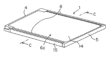
도 1은 본 발명에 따른 IC 카드의 전체 사시도이고, 도 2는 상기 IC 카드의 내부구성을 도시하는 분해 사시도이며, 도 3은 도 1의 A-A선 단면을 도시하는 단면도이고, 도 4는 도 1의 B-B선 단면을 도시하는 단면도이다. 또한, 도 5는 상기 IC 카드의 구성요소의 하나인 제 1 패널(전면 패널)의 정면도이다.1 is an overall perspective view of an IC card according to the present invention, FIG. 2 is an exploded perspective view showing the internal configuration of the IC card, FIG. 3 is a cross-sectional view showing a cross section taken along the line AA of FIG. It is sectional drawing which shows the BB line cross section of. 5 is a front view of a first panel (front panel) which is one of the components of the IC card.
도 1에서 명백한 바와 같이, 이 IC 카드의 외형은 박판의 대략 직방체 형태이고, 그 확대면(상부표면 또는 하부표면)은 대략 장방형의 형태를 하고 있다. 이하에서는, 상기 IC 카드에 있어서의 위치관계를 명확히 하기위해서, 도 1내의 X1-X2 방향, 즉 상기 IC 카드의 대략 장방형의 확장면의 긴 변 방향을 「카드길이 방향」이라고 하여, X1측, X2측을 각기 「전」, 「후」라는 것으로 한다. 또한, 도 1의 Y1-Y2 방향, 즉 상기 대략 장방형의 확장면의 짧은 변 방향을 「카드폭방향」이라고 하여, Y1측, Y2측을 각기 「좌(왼쪽)」, 「우(오른쪽)」이라는 것으로 한다. 또한, 도 1내의 Z1-Z2 방향을 「카드두께 방향」이라고 하여, Z1측, Z2측을 각기 「상(위)」, 「하(밑)」라는 것으로 한다. 또, 이 위치관계의 표시방법은, 기본적으로는 다른 실시예의 형태에 있어서도 같다.As is apparent from Fig. 1, the IC card has an external rectangular parallelepiped shape, and its enlarged surface (upper surface or lower surface) has a substantially rectangular shape. In the following, in order to clarify the positional relationship in the IC card, the X1-X2 direction in Fig. 1, that is, the long side direction of the substantially rectangular expansion surface of the IC card is referred to as the "card length direction". Assume that the X2 side is "before" and "after", respectively. In addition, the Y1-Y2 direction of FIG. 1, ie, the short side direction of the said substantially rectangular extended surface is called "card width direction", and Y1 side and Y2 side are respectively "left (left)" and "right (right)". It is called. In addition, let Z1-Z2 direction in FIG. 1 be called "card thickness direction", and let Z1 side and Z2 side be "upper" and "lower", respectively. In addition, the display method of this positional relationship is basically the same also in the form of another Example.
도 1∼도 5에 있어서, (1)은 IC 카드이고, (2)는 IC(집적회로)를 포함하고 있는 전자부품(복수)이고, (3)은 이들 전자부품(2)을 탑재하고 있는 기판이다. (4)는 상기 기판(3)에 접속되는 한편 시스템기기 내지는 외부기기(도시하지 않음)와의 신호의 수수를 행하는 커넥터이고, (5)는 상기 커넥터(4)와 전자부품(2)을 탑재하고 있는 기판(3)을 격납·유지하는 수지제(樹脂製)의 테두리체(frame)이다. 이 IC 카드(l)에서는, 각 전자부품(2)은 기판(3)의 한 면(하면)만큼 장착되고 있다.1 to 5, (1) is an IC card, (2) is an electronic component (plural) containing an IC (integrated circuit), and (3) is mounted on these
수지제의 테두리체(5)는 그 하단부에 위치하는 평판 형상의 하부판부(5a)와, 그 좌우(카드폭방향)의 양단부에 위치하여 각기 카드길이 방향으로 신장하는 2개의 측테두리부(5b)와, 그 후단부에 위치하여 카드폭방향으로 신장하는 후테두리부(5c)로 이루어지고, 이것들의 각부(5a, 5b, 5c)는 일체적으로 형성되어 있다. 이 테두리체(5)는, 예컨대 폴리부틸렌 테레프탈레이트(PBT)수지, 폴리카보네이트(PC)수지 등을 사용하여 성형가공으로 제조된다.The
(6c)는 테두리체(5)의 상부표면(제 1의 테두리체 단면)과 계합하여, IC 카드(1)의 대략 장방형의 상측 확장면을 이루는 금속제의 제 1 패널(전면 패널)이다. 또한, (6d)는 테두리체(5)의 하부표면(제 2의 테두리체 단면)과 계합하여, IC 카드(1)의 대략 장방형의 하측 확장면을 이루는 금속제의 제 2 패널(후면 패널)이다. 이 IC 카드(1)에 있어서는, 양 패널(6c, 6d)은 테두리체(5)에 대하여 직접 취부되고, 종래의 IC 카드로 사용되고 있는 접착지(도 35또는 도 36참조)는 사용되고 있지는 않는다. 여기서, 제 1 패널(6c)은, 바람직하게 스테인리스강(stainless steel)으로 형성되어 있다. 또한, 제 2 패널(6d)은 바람직하게 스테인리스강으로 형성되어 있지만, 알루미늄(aluminium)으로 형성되어도 좋다.6c is a metal first panel (front panel) which engages with the upper surface (first frame end face) of the
커넥터(4)는 전자부품(2)을 탑재하고 있는 기판(3)에 납땜에 의해 취부되고 있다. 또, 커넥터(4)와 기판(3)은 커넥터(4)에 설치된 커넥터측 접속부(l2)(복수)와 기판(3)에 설치된 기판측 접속부(13)(복수)를 결합함에 의해 전기적으로 접속되어 있다. 그리고, 커넥터(4)와 기판(3)이 결합되는 조립체(일반적으로, 모듈(module)이라고 지칭된다)는 압입 혹은 코킹(caulk joining) 등에 의해 테두리체(5)에 취부된다.The
제 1 패널(6c)은 그 전단부 부근의 약간의 영역을 제외하고 그 좌우의 양 단부 영역의 각각을, 측테두리부(5b)의 외면형상에 대응하여 2회 절곡한 후에 그 앞단부를 측테두리부(5b)의 하단면에 계합시키므로써, 접착지를 쓰지않고서 테두리체(5)에 직접 취부되고 있다. 즉, 제 1 패널(6c)은 테두리체(5)에 취부되기 전에 이미 측테두리부(5b)의 외면형상에 대응하도록 2회 절곡되고, 상기 제 1 패널(6c)에는 확장부(14)와 측부(15)와 훅크부(16)가 형성되어 있다. 그리고 제 1 패널(6c)을 테두리체(5)에 취부시킬때는 양 측부(15)를 손으로 또는 적당한 도구 등을 사용하여 좌우로 확대하면서 상기 제 1 패널(6c)을 측테두리부(5b)에 끼워 넣어, 훅크부(16)(앞단부)를 측테두리부(5b)의 하부표면에 계합시킨다. 이에 따라, 제 1 패널(6c)은 테두리체(5)에 확실히 고정된다. 또, 측테두리부(5b)의 표면은, 뒤(후) 테두리부(5c)의 상부표면보다도 제 1 패널(6c)의 두께 만큼 높이가 낮게 되도록 단차가 형성되어 있다. 따라서, 제 1 패널(6c)을 테두리체(5)에 취부한 후에 있어서는, IC 카드(1)의 상측 확장면은 평판 상태로 된다. 즉, 제 1 패널(6c)의 상부표면과 뒤(후)테두리부(5c)의 상부표면과의 사이에 단차가 생기지 않는다. 한편, 제 2 패널(6d)은 테두리체(5)의 하부판부(5a)의 하부표면에 접착재를 사용하여 취부되고있다. 또, 제 2 패널(6d)에는 테두리체(5)에 취부되기 전에 접착재가 부착될 수 있다. 상기 제 2 패널(6d)은 용이하게 테두리체(5)에 부착될 수 있다.The
따라서, 본 발명에 따른 IC 카드(1)에 있어서는, 종래의 IC 카드에 비교해서 접착지를 쓰지 않은 부품의 부품점수가 작아져, 상기 IC 카드(1)의 구조가 간소화된다. 또한, 종래의 IC 카드의 경우와 같은 접착지의 패널로의 임시 부착을 행할 필요가 없고, 또한 특별한 장치를 사용해 패널(6c, 6d)을 테두리체(5)에 압착시킬 필요도 없기때문에, 상기 IC 카드(l)의 제조 방법이 간략화된다.Therefore, in the
또한, IC 카드(1)의 좌우의 양측면이 제 1 패널(6c)에 의해서 덮여지기 때문에, 상기 IC 카드(l)의 전자파에 대한 성능, 예컨대 전자파차단성이 높아진다. 또한, IC 카드(1)에 대전한 전하를 그 좌우의 측면에 의해 어스(earth)하는 형식의 커넥터(4)를 사용하는 경우는, 개별의 접점을 상기 IC 카드(1)에 설치하지 않더라도 어스(earth)를 잡을 수 있다(즉, 전하가 방전될 수 있다). 또한, 제 1 패널(6c)과 제 2 패널(6d)은, 테두리체(5)의 하부표면에서 접촉하고 있기때문에, 양 패널(6c, 6d)이 서로 전기적으로 도통상태로 된다. 따라서, 개별의 패널 도통기구를 마련하는 일 없이, ESD 대책(정전기대책)을 실현할 수가 있다.In addition, since the left and right side surfaces of the
(실시예 2)(Example 2)
도 2에 도시된 바와 같이 상기 IC 카드(1)에 있어서는, 제 1 패널(6c)의 확장부(14)가, 상기 제 1 패널(6c)이 테두리체(5)로부터 분리되고 있는 상태에 있어서 카드길이 방향과 수직인 평면으로 절단하였을 때의 단면이 하방향으로 돌출만곡하는 곡선적 형상을 보이는 것 같은 형상으로 형성되는 것이 바람직하다. 이와 같이 하면, 제 1 패널(6c)을 테두리체(5)에 취부한 상태에 있어서는, 본래는 곡면 형상의 확장부(14)가 탄성적 변형에 의해 도 1에 도시되는 바와 같이 평면 형상으로 되고, 이때 제 1 패널(6c)내에는 확장면(l4)을 원래의 곡면 형상으로 되돌리고자 하는 탄성력 내지는 복원력이 생긴다. 이 탄성력 내지는 복원력은, 제 1 패널(6c)을 테두리체(5)에 향해서 가압 부착하는 방향으로 작용하기 때문에, 이 탄성력 내지는 복원력에 의해서 제 1 패널(6c)이 테두리체(5)에 강하게 부착된다. 따라서, 제 1 패널(6c)은 테두리체(5)에 밀착되고, 패널 분리의 발생이 방지된다.As shown in FIG. 2, in the
(실시예 3)(Example 3)
도 5에 도시된 바와 같이, 상기 IC 카드(1)에 있어서는, 제 1 패널(6c)이, 상기 제 1 패널(6)이 테두리체(5)로부터 분리되고 있는 상태에 있어서 카드길이 방향과 수직인 평면으로 절단하였을 때의 단면형상에서 볼때, 확장면(14)과 측부(15)로 형성되는 절곡부의 절곡 각도θ가 예각을 이루는 것 같은 형상으로 형성되는 것이 바람직하다. 이와 같이 하면, 제 1 패널(6c)을 테두리체(5)에 취부한 상태에 있어서, 본래 예각상태인 상기 절곡부가 탄성적 변형에 의해 직각상태로 되고(측테두리부(5b)의 각부가 직각이니까), 이때 상기 절곡부에는 이것을 원래의 예각상태에 되돌리고자 하는 탄성력 내지는 복원력이 생긴다. 이 탄성력 내지는 복원력은 제 1 패널(6c)을 테두리체(5)에 향해서 가압 부착하는 방향, 즉 훅크시키는 방향으로 작용하기 때문에, 이 탄성력 내지는 복원력에 의해 제 1 패널(6c)은 테두리체(5)에 밀착되어, 패널 분리의 발생이 방지된다.As shown in Fig. 5, in the
(실시예 4)(Example 4)
도 3 및 도 4에 도시된 바와 같이, 상기 IC 카드(1)에 있어서는, 제 2 패널(6d)은 제 1 패널(6c)보다도 판두께가 얇은 재료로 형성되는 것이 바람직하다. 즉, 제 1 패널(6c)은 테두리체(5)에 대하여 확실히 훅크될 수 있도록 매우 강한 탄성력 내지는 복원력을 생기게 하기위해서, 0.2 mm 정도의 판두께를 필요로 한다. 그러나, 제 2 패널(6d)은 테두리체(5)(하부판부(5a))의 하부표면에 부착될 뿐이기때문에, 그다지 두께를 필요로 하지 않는다. 이것 때문에, 제 2 패널(6d)의 두께는 0.05 mm 정도로 하는 것이 바람직하다. 이와 같이 하면, 제 2 패널(6d)의 재료비가 저감되어, 상기 IC 카드(1)의 제조 비용이 저감된다.As shown in Figs. 3 and 4, in the
(실시예 5)(Example 5)
도 6은 본 발명의 실시예 5에 따른 IC 카드의 외관을 도시한 사시도이고, 도 8은 도 6의 C-C 선 단면을 도시한 단면도이다. 도 6 및 도 8에 도시된 바와 같이, IC 카드(1)에 있어서는, 제 1 패널(6c)의 확장부(14)의 좌우의 양단부영역의 각각에, 카드길이 방향으로 신장되고, 또한 하방향(테두리체측)으로 향해서 대략 U 자 형상 또는 대략 V 자 형상으로 돌출되며, 테두리체(5)의 측테두리부(5b)의 상부표면과 계합하는 리브(8)가 형성되어 있다. 이 IC 카드(1)에 있어서는, 리브(8)에 의해서 제 1 패널(6c)의 강도가 높아지고, 나아가서는 상기 IC 카드(1)의 강도가 높아진다. 또한, 리브(8)에 의해서 제 1 패널(6c)과 테두리체(5)와의 계합성이 높아진다.FIG. 6 is a perspective view showing the appearance of an IC card according to
여기서, 리브(8)는, 제 1 패널(6c)을 테두리체(5)에 취부한 후에 형성·가공하는 것이 바람직하다. 또, 리브(8)는, 널리 알려져 있는 보통의 방법, 예컨대 확장면(14)의 소정의 부분을 형금(dies) 등으로 하방향으로(테두리체측에 향해서) 타출(striking) 혹은 압출(pressing)하는 방법으로 형성된다. 이와 같이 하면, 제 1 패널(6c)의 확장부(14)의 좌우의 치수가 약간 크게 형성되어 있더라도, 리브형성시에 상기 확장부(14)가 좌우로 약간 줄어들기 때문에, 제 1 패널(6c)과 측테두리부(5b)와의 사이의 밀착성이 높아진다.Here, it is preferable to form and process the
(실시예 6)(Example 6)
도 7 및 도 8에 도시된 바와 같이, 제 1 패널(6c)의 확장부(14)에 리브(8)가 설치되는 경우는, 상기 리브(8)와 대응하는 위치에 있어서의 측테두리부(5b)의 상부표면에, 상기 리브(8)와 계합하는 리브용 홈부(9)가 설치되는 것이 바람직하다. 이 리브용 홈부(9)는 리브(8)를 형성할 때의 상기 리브(8)의 후퇴 장소이고, 테두리체(5)의 성형시에 형성될 수 있다. 이와 같이 하면, 제 1 패널(6c)을 테두리체(5)에 취부한 후에 리브(8)를 형성·가공할 때, 상기 리브(8)의 형성·가공이 확실하고 용이하며, 또한 리브(8)의 깊이(높이)의 조정이 용이하게 된다.As shown in FIG. 7 and FIG. 8, when the
(실시예 7)(Example 7)
도 9에 도시된 바와 같이, 실시예 7의 IC 카드(1)에 있어서는, 제 1 패널(6c)의 확장부의 좌우의 양단부 부근의 각각에, 하방향으로(테두리체측으로 향해서) 돌출되어 상기 테두리체(5)의 측테두리부(5b)와 계합하는 복수의 돌기(10)가 형성되어 있다. 이 경우, 돌기(10)에 의해서 제 1 패널(6c)과 테두리체(5)와의 밀착성이 높아진다. 또한, 돌기(l0)에 의해서 제 1 패널(6c)과 테두리체(5)와의 사이에 미끄럼이 생기는 것이 방지되어, 상기 IC 카드(1)의 전체로서의 강도가 높아진다. 여기서, 돌기(10)는, 제 1 패널(6c)을 테두리체(5)에 취부한 후에 형성된다. 또, 돌기(10)는, 널리 알려져 있는 보통의 방법, 예컨대 확장부(14)의 소정의 부분을 형금 등으로 하방향으로(테두리체측으로 향해서) 타출 또는 압출하는 방법으로 형성된다.As shown in Fig. 9, in the
도 10에 도시된 바와 같이, 제 1 패널(6c)의 양측부(15)의 각각에, 좌방향 또는 우(오른쪽)방향으로(테두리체측으로 향해서) 돌출되어 상기테두리체(5)의 측테두리부(5b)와 계합하는 복수의 돌기(10a)가 형성되어도 좋다. 이 경우도, 돌기(10a)에 의해서 제 1 패널(6c)과 테두리체(5)와의 밀착성이 높아지고, 또한 제 1 패널(6c)과 테두리체(5)와의 사이에 미끄럼이 생기는 것이 방지되어 IC 카드(1)의 전체로서의 강도가 높아진다. 또, 이 돌기(l 0a)는, 제 1 패널(6c)을 테두리체(5)에 취부한 후에 형성된다.As shown in Fig. 10, each of the
(실시예 8)(Example 8)
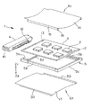
도 11은 본 발명의 실시예 8에 따른 IC 카드의 전체 사시도이다. 또한, 도 12는 도 1의 J-J 선 단면을 도시하는 단면도이고, 도 13은 도 11의 K-K 선 단면을 도시하는 단면도이고, 도 14는 상기 IC 카드의 내부구성을 도시하는 분해 사시도이다.11 is an overall perspective view of an IC card according to
도 11∼도 14에 도시한 바와 같이, 이 IC 카드(1)에 있어서는, 기본적으로는, 제 2 패널(6h)이, 그 전단부 부근의 약간의 부분을 제외하고 좌우의 양 단부(30)의 각각을, 측테두리부(5b)의 외면에 대응하여 절곡하므로써, 테두리체(5)에 직접 취부되고 있다. 여기서, 측테두리부(5b)의 하반부의 좌우의 양단부 부근의 각각에는, 제 2 패널(6h)의 좌우의 단부(30)보다도 좌우방향내측까지 절결되어 있는 절결부(32)가 설치되어 있다. 따라서, 제 2 패널(6h)이 테두리체(5)에 취부된 상태에 있어서, 양 단부(30)는 절결부(32)의 벽부에 접촉할 때까지는 안쪽으로 변위(이동) 할 수가 있다. 한편, 제 1 패널(6c)은, 그 전단부 부근의 약간의 부분을 제외하고 좌우의 양단부영역의 각각을, 제 2 패널(6h)의 측부 및 확장부(17)의 일부를 덮도록 하여, 테두리체 외면 내지는 제 2 패널 외면에 대응하여 2회 절곡한 후에 그 훅크부(l6)를 제 2 패널(6h)의 확장부(17)의 하부표면에 접촉시키므로써, 테두리체(5)에 직접 취부되고 있다. 또, 이 테두리체(5)에 있어서는, 기판(3)의 상하 양면에 전자부품(2)이 탑재되고 있는 관계로, 실시예 1 내지 7의 경우와 같은 하부판부(5a)는 설치되지 않는다. 그 대신, 테두리체(5)에는, 그 강도를 높이기 위해서 앞테두리부(5f)가 설정되고 있다.As shown in Figs. 11 to 14, in the
이 IC 카드(1)는 커넥터(4)를 통해 시스템기기(외부기기)측에 접속되며, 이것에 의해서 시스템기기의 메모리 용량이 확장되거나 또는 기능이 확장된다. 또, 이 IC 카드(1)의 조립에 있어서는, 우선 기판(3)과 커넥터(4)가 납땜 등에 의해 전기적·기계적으로 접속되고, 이들이 테두리체(5)에 격납 내지는 유지된다. 그리고, 제 2 패널(6h)이 테두리체(5)에 임시로 부착된 후, 제 1 패널(6c)이 IC 카드(1)의 상부표면을 덮고, 또한 상기 제 1 패널(6c)의 양측면이 테두리체(5)의 양측부를 덮고, 이 다음 제 1 패널(6c)이 테두리체(5)에 기계적으로 고정된다.The
이 IC 카드(1)로서는, 양 패널(6c, 6h)가 양쪽 모두 측테두리부(5b)의 외면에 따라 절곡되면서 테두리체(5)에 계합되고 있기 때문에, 접착재료(예컨대, 접착지)를 쓰지않고서, 양 패널(6c, 6h)을 테두리체(5)에 취부시킬 수 있다. 따라서, IC 카드(1)의 구조가 간소화됨과 동시에 그 제조 방법이 간략화된다. 또한, 제 2 패널(6h)의 좌우의 양단부(30)가 제 1 패널(6c)에 의해서 덮여지기 때문에, 상기 IC 카드(1)의 외관은 우수하다. 또, 실시예 1에 따른 IC 카드(1)의 경우와 같이, 전자파에 대한 성능이 높아지고, 개별의 접점을 마련하지 않더라도 어스(earth)를 잡을 수 있고, 또한 개별의 패널 도통기구를 마련하는 일 없이 ESD 대책을 실현할 수가 있는 것은 물론이다.As the
또, 이 IC 카드(1)에 있어서는, 양 패널(6c, 6h)을 IC 카드 본체측 내지는 테두리체(5)에 확실히 밀착시킬 필요가 있으며, 특히 카드폭방향의 중앙부에서의 밀착성을 높일 필요가 있다. 그리고, 이 IC 카드(1)에 있어서는, 상기 구성에 의해 이러한 밀착성이 양호하지만, 또 개량의 여지가 있는 것으로 생각된다. 또한, 이 IC 카드(1)에 있어서, 커넥터(4)는, 그 귀부(41)를 테두리체(5)의 전단부 부근에 설치된 커넥터 끼워 맞춤 볼록부(51)에 압입함에 의해, 혹은 테두리체(5)에 설치된 훅크를 커넥터(4)의 귀부에 고정함에 의해, 테두리체(5)에 고정되지만, 커넥터(4)와 테두리체(5)와의 사이의 취부강도에는 개량의 여지가 또한 있는 것으로 생각된다.Moreover, in this
(실시예 9)(Example 9)
도 15는 본 발명의 실시예 9에 따른 IC 카드의 구성을 도시한 분해 사시도이고, 도 16은 도 15에 도시한 IC 카드의 조립후에 있어서의 D-D 선 단면(횡단면)을 도시한 단면도이다. 또한, 도 17은 도 15에 도시한 IC 카드의 조립후에 있어서의 E-E 선 단면(종단면)을 도시한 단면도이다.Fig. 15 is an exploded perspective view showing the configuration of the IC card according to the ninth embodiment of the present invention, and Fig. 16 is a cross-sectional view showing a D-D line cross section (lateral cross section) after assembling the IC card shown in Fig. 15. 17 is a cross-sectional view showing the E-E line cross section (vertical cross section) after assembling the IC card shown in FIG.
도 15∼도 17에 도시된 바와 같이, 이 IC 카드(1)에 있어서는, 기본적으로는, 제 2 패널(6e)가, 그 전단부 부근의 약간의 영역을 제외하고 그 좌우의 양단부영역의 각각을, 측테두리부(5b)의 외면형상에 대응하여 2회 절곡한 후에 그 앞단부를 측테두리부(5b)의 상부표면에 계합시키므로써, 테두리체(5)에 직접 취부되고 있다. 한편, 제 1 패널(6c)은 그 전단부 부근의 약간의 영역을 제외하고 그 좌우의 양단부 영역의 각각을, 측테두리부(5b)의 외면형상에 대응하여 2회 절곡한 후에 그 앞단부를 측테두리부(5b)의 하부표면에 계합시키므로써, 접착지를 쓰지 않고서 테두리체(5)에 직접 취부되고 있다.As shown in Fig. 15 to Fig. 17, in the
보다 상세하게는, 이 IC 카드(1)에 있어서 카드폭방향에서 볼때 양측테두리부(5b)의 각각의 외면에, 카드폭방향 바깥쪽으로 볼록 형상으로 되는 볼록부(5d)와, 같은 방향으로 오목 형상으로 되는 오목부(5e)가 형성되어 있다. 이 테두리체(5)에 있어서는, 기판(3)의 상하양면에 전자부품(2)이 탑재되고 있는 관계로, 실시예 1∼7의 경우와 같은 하부판부(5a)는 설치되지 않는다. 그 대신, 테두리체(5)에는, 그 강도를 높이기 위해서 앞테두리부(5f)가 설치된다.More specifically, in the
그리고, 제 2 패널(6e)의 좌우의 양단부(18)의 각각에는, 복수의 돌기부(18a)와 복수의 볼록부(18b)가, 카드길이 방향으로 교대로 나란히 형성되어 있다. 여기서, 돌기부(18a)는 오목부(5e)의 외면형상에 대응하여 2회 절곡된 후에 그 앞단부를 측테두리부(5b)의 상부표면에 계합시키므로써, 테두리체(5)에 직접 취부되고 있다. 또한, 볼록부(5d)는, 측테두리부(5b)의 하부표면에 형성된 도랑에 끼워 넣어져 있다. 또, 제 2 패널(6e)의 확장부(17)는 제 1 패널(6c)의 확장부(l4)와 같이 테두리체(5)로의 밀착성을 높이기위해서 만곡형상으로 되어 있다(단, 만곡방향은 상하반대).In each of the left and right ends 18 of the
한편, 제 1 패널(6c)은 제 2 패널(6e)의 좌우의 측부를 덮도록 하여, 볼록부(5d)의 외면형상에 대응하여 2회 절곡한 후에 훅크부(16)(앞단부)를 측테두리부(5b)의 하부표면에 계합시키므로써, 테두리체(5)에 직접 취부되고 있다. 따라서, 이 IC 카드(l)에서, 양 패널(6c, 6e)을 테두리체(5)에 취부시킬 때는, 우선 제 2 패널(6e)의 좌우의 양측부를 손 또는 적당한 도구 등을 사용하여 좌우로 확대하면서 상기 제 2 패널(6e)의 돌기부(18a)를 오목부(5e)에 끼워 넣고, 돌기부(18a)의 앞단부를 측테두리부(5b)의 상부표면에 계합시킨다. 이에 따라, 제 2 패널(6e)의 테두리체(5)로의 설치가 완료된다. 다음에, 제 l 패널(6c)의 양측부(15)를 손 또는 적당한 도구 등을 사용하여 좌우로 확대하면서 상기 제 1 패널(6c)을 볼록부(5d)에 끼워 넣고, 훅크부(16)(앞단부)를 측테두리부(5b)의 하부표면에 계합시킨다. 이에 따라, 제 1 패널(6c)의 테두리체(5)로의 설치가 완료된다.On the other hand, the
이 IC 카드(l)에서는, 양 패널(6c, 6e)이 양쪽 모두 측테두리부(5b)의 외면에 따라 절곡되면서 테두리체(5)에 계합되므로, 접착재료(예컨대, 접착지)를 쓰지않고서, 양 패널(6c, 6e)을 테두리체(5)에 취부시킬 수 있다. 따라서, IC 카드(1)의 구조가 간소화됨과 동시에 그 제조 방법이 간략화된다. 또한, 제 2 패널(6e)의 좌우의 양단부(18)가 제 1 패널(6c)에 의해서 덮여지고, 혹은 측테두리부(5b)의 홈내에 몰입되기 때문에, 상기 IC 카드(1)의 외관이 우수하게 된다. 또, 실시예 1에 따른 IC 카드(1)의 경우와 같이, 전자파에 대한 성능이 높아지고, 개별의 접점을 마련하지 않더라도 어스(earth)를 잡을 수 있고, 개별의 패널 도통기구를 마련하는 일 없이 ESD 대책을 실현할 수가 있는 것은 물론이다.In this
(실시예 10)(Example 10)
도 18은 본 발명의 실시예 10에 따른 IC 카드의 구성을 도시한 분해 사시도이고, 도 19는 도 18에 도시한 IC 카드의 구성요소의 하나인 제 1 패널의 정면도이다. 또한, 도 20은 도 18에 도시한 IC 카드의 조립후에 있어서의 횡단면도(카드길이 방향과 직교하는 평면으로 절단한 단면도)이고, 도 21은 도 18에 도시한 IC 카드의 조립후에 있어서의 종단면도(카드폭방향과 직교하는 평면으로 절단한 단면도)이다.FIG. 18 is an exploded perspective view showing the configuration of the IC card according to the tenth embodiment of the present invention, and FIG. 19 is a front view of a first panel which is one of the components of the IC card shown in FIG. 20 is a cross sectional view (sectional view cut | disconnected in the plane orthogonal to a card length direction) after assembly of the IC card shown in FIG. 18, and FIG. 21 is a longitudinal cross-sectional view after assembly of the IC card shown in FIG. (Sectional drawing cut in the plane orthogonal to a card width direction).
도 18∼도 21에 도시된 바와 같이, 이 IC 카드(1)에 있어서는, 제 1 패널(6f)이 확장부(14)의 광폭부(제 1 패널(6f)의 대부분을 차지한다)로, 그 좌우의 양단부영역의 각각을, 측테두리부(5b)의 외면형상에 대응하여 2회 절곡한 후에 훅크부(16)(앞단부)를 측테두리부(5b)의 하부표면측에 계합시키므로써, 접착지를 쓰지않고서 테두리체(5)에 직접 취부되고 있다. 또, 제 l 패널(6f)의 테두리체(5)로의 취부 방법은 기본적으로는 실시예 1의 경우와 같다.As shown in Figs. 18 to 21, in the
그리고, 확장부(14)의 광폭부의 좌우의 양단부영역의 각각에, 카드길이 방향으로 신장되고 또한 하방향(테두리체측)으로 대략 U 자 형상 또는 대략 V 자 형상으로 돌출되어 측테두리부(5b)와 계합하는 리브(20)가 형성되어 있다. 또, 이 리브(20)의 기능은 실시예 5의 리브(8)의 경우와 같다. 또한, 확장부(14)의 광폭부의 바로 앞측에 이것과 인접하게 상기 광폭부보다도 좌우의 길이가 짧은 협폭부가 설치되며, 협폭부의 좌우의 양단부의 각각에, 상기 리브(20)의 대략 U 자 형상 또는 대략 V 자 형상으로 오목한 골형상 부분(20a, 20b) 중의 좌우방향내측에 위치하는 쪽의 경사부분(20a)이 전방향으로 연장 설치되는 보강 리브(21)가 설치된다.Then, in each of the left and right both end regions of the wide portion of the widening
이 IC 카드(1)에 있어서는, 리브(20)가 설치되지 않은 확장부(14)의 협폭부의 강도가 보강 리브(21)에 의해서 높아지고 상기 협폭부가 테두리체(5)로부터 분리되는 것이 방지되고, 나아가서는 제 1 패널(6f)의 강도가 높아진다. 또, 실시예 1의 경우와 같이, 전자파에 대한 성능이 높아지고, 개별의 접점을 마련하지 않더라도 어스(earth)를 잡을 수 있고, 개별의 패널도통기구를 마련하는 일 없이 ESD 대책을 실현할 수가 있는 것은 물론이다.In this
(실시예 11)(Example 11)
도 18 및 도 20으로부터 명백한 바와 같이, 본 발명의 실시예 11에 따른 IC 카드(l)에서는, 제 2 패널(6g)이, 그 전단부 부근의 약간의 부분을 제외하고 좌우의 양단부(23)의 각각을, 측테두리부(5b)의 외면에 대응하여 절곡하므로써, 테두리체(5)에 직접 취부되고 있다. 여기서, 측테두리부(5b)의 하반부의 좌우의 양단부 부근의 각각에는, 제 2 패널(6g)의 좌우의 단부(23)보다도 좌우방향내측까지 절결되어 있는 절결부(24)가 설치된다. 따라서, 제 2 패널(6g)이 테두리체(5)에 취부된 상태에 있어서, 양단부(23)는 절결부(24)의 벽부에 접촉할 때까지는 안쪽으로 변위(이동)될 수가 있다. 또, 이와 같이 양단부(23)가 안쪽으로 변위한 때에는 제 2 패널(6g)의 확장부(22)가 아래쪽으로 돌출·만곡하는 것은 물론이다(도 22 및 도 23 참조). 그리고, 제 1 패널(6f)은, 그 전단부 부근의 약간의 부분을 제외하고 좌우의 양단부영역의 각각을, 제 2 패널(6g)의 측부 및 확장부(22)의 일부를 덮도록 하여, 테두리체 외면 내지는 제 2 패널 외면에 대응하여 2회 절곡한 후에 그 훅크부(16)를 제 2 패널(6g)의 확장부(22)의 하부표면에 접촉시키므로써, 테두리체(5)에 직접 취부되고 있다.As is apparent from Figs. 18 and 20, in the
이 IC 카드(1)에 있어서는, 이것을 조립하는 경우, 제 2 패널(6g)이 테두리체(5)에 취부된 후에 제 1 패널(6f)이 테두리체(5)에 취부되는 것으로 된다. 여기에 있어, 제 1 패널(6f)을 테두리체(5)에 취부할 때는, 이미 테두리체(5)에 취부되고 있는 제 2 패널(6g)을 하방향으로 만곡하도록 탄성변형시키므로써, 혹은 제 2 패널(6g)에 카드폭방향의 압축력을 가하는 것에 의해, 제 2 패널(6g)의 카드폭방향에서의 양단부(23)를 일시적으로 좌우방향내측으로 변위시키는 것이 바람직하다.In this
도 22 및 도 23에 도시된 바와 같이, 이 경우, 제 2 패널(6g)의 카드폭방향의 길이가 일시적으로 줄어들기때문에, 제 1 패널(6f)를 카드폭방향의 J 바깥쪽으로 그다지 크게 확대하지 않고서 테두리체(5)에 취부될 수 있다. 이것 때문에, 제 l 패널(6f)를 테두리체(5)에 취부할 때에 상기 제 1 패널(6f)가 영구변형영역, 즉 소성변형영역에 도달 할 수가 있다. 그 결과, 제 1 패널(6f)의 제 2 패널(6g)의 하단부로의 계합길이 내지는 훅크길이 L(도 20참조)를 크게 할 수 있어, 제 1 패널(6f)의 테두리체(5)로의 설치를 확실히 할 수가 있다. 또, 도 22 및 도 23내에서, 화살표 f1∼f3는, 제 1 패널(6f)을 취부시킬 때에, 제 2 패널(6g)에 가해야 되는 힘의 방향을 도시하고 있다. 이 실시예 11에 있어서도, 실시예 2의 경우와 같이, IC 카드(1)의 구조가 간소화됨과 동시에 그 제조 방법이 간략화되어, 그 외관이 우수하며, 전자파에 대한 성능이 높아지고, 개별의 접점을 마련하지 않더라도 어스(earth)를 잡을 수 있으며, 개별의 패널도통기구를 마련하는 일 없이 ESD 대책을 실현할 수가 있는 것은 물론이다.As shown in Figs. 22 and 23, in this case, since the length of the
(실시예 12)(Example 12)
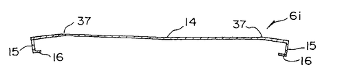
도 24는 본 발명의 실시예 12에 따른 IC 카드의 전체 사시도이고, 도 25는 상기 IC 카드의 내부구성을 도시한 분해 사시도이다. 또한, 도 26도 및 도 27은 각기 상기 IC 카드의 구성요소의 하나인 제 1 패널(전면 패널) 및 제 2 패널(후면 패널)의 IC 카드본체로의 취부전의 상태(형상)를 도시한 횡단면도이다.24 is an overall perspective view of an IC card according to a twelfth embodiment of the present invention, and FIG. 25 is an exploded perspective view showing an internal configuration of the IC card. 26 and 27 are cross sectional views showing the state (shape) of the first panel (front panel) and the second panel (rear panel), which are one of the components of the IC card, before mounting to the IC card body. to be.
도 24도∼도 27도에 도시된 바와 같이, 이 IC 카드(1)에 있어서는, 기본적으로는 실시예 8의 경우와 같이, 제 2 패널(6j)이, 그 전단부 부근의 약간의 부분을 제외하고 좌우의 양단부(30)의 각각을, 측테두리부(5b)의 외면에 대응하여 절곡한 것에 의해, 테두리체(5)에 직접 취부되고 있다. 한편, 제 1 패널(6i)은, 그 전단부 부근의 약간의 부분을 제외하고 좌우의 양단부영역의 각각을, 제 2 패널(6j)의 측부 및 확장면(17)의 일부를 덮도록 하여, 테두리체 외면 내지는 제 2 패널 외면에 대응하여 2회 절곡한 후에 그 훅크부(16)를 제 2 패널(6j)의 확장부(17)의 하부표면에 접촉시키므로써, 테두리체(5)에 직접 취부되고 있다.As shown in FIG. 24 to FIG. 27, in this
그리고, 제 1 패널(6i)의 확장부(14)는, 상기 제 1 패널(6i)이 테두리체(5)로부터 분리되고 있는 상태에 있어서 카드길이 방향과 수직인 평면으로 절단하였을 때의 단면이 카드폭방향에서 볼때 양단부 부근의 측테두리부(5b)에는 걸리지 않은 위치에 각기 바깥쪽으로(상방향으로) 돌출하는 볼록부(37)를 갖는 것 같은 형상으로 형성되어 있다. 한편, 제 2 패널(6j)의 확장부(17)는, 상기 제 2 패널(6j)이 테두리체(5)로부터 분리되고 있는 상태에 있어서 카드길이 방향과 수직인 평면으로 절단하였을 때의 단면이 카드폭방향에서 볼때 양단부 부근의 측테두리부(5b)에는 걸리지 않은 위치에 각기 바깥쪽으로(하방향으로) 돌출하는 볼록부(38)를 갖는 것 같은 형상으로 형성되어 있다. 예컨대, 양 패널(6i, 6j)에는, 각기, 카드폭방향에서 볼때 그 좌우단의 절곡부 보다도 안쪽으로서, 측테두리부(5b)를 껴안는 부분보다도 안쪽으로 되는 위치에 있어서의, 좌우 2개 장소에 볼록부(37, 38)가 설치된다. 또, 양 패널(6i, 6j)의 확장부(14, 17)는 상기 양 패널(6i, 6j)이 테두리체(5)로부터 분리되고 있는 상태에 있어서는, 카드폭방향에서 볼때 양 볼록부(37, 38)사이에서 평면형상을 보이도록, 즉 횡단면으로 보면 직선형상이 되도록 형성되어 있다.The expanded
이 IC 카드(1)로서는, 제 1 패널(6i)을 테두리체(5)에 취부한 상태에 있어서는, 본래는 곡면형상의 확장부(14)가 탄성적 변형에 의해 평면형상으로 되고, 이 때 제 1 패널(6i)내에는 확장부(14)를 원래의 곡면형상으로 되돌리고자 하는 탄성력이 생긴다. 이 탄성력은, 제 1 패널(6i)를 테두리체(5)를 향해서 강하게 압착 부착하는 방향으로 작용하기 때문에, 이 탄성력에 의해서 제 1 패널(6i)은 테두리체(5)에 강하게 압착하여 부착된다. 따라서, 제 1 패널(6i)은 테두리체(5)에 확실히 밀착된다. 이것과 마찬가지로, 제 2 패널(6j)도 테두리체(5)에 확실히 밀착된다.As the
예컨대, 이 IC 카드(1)에 있어서는, 제 1 패널(6i)의 카드폭방향 양단의 절곡부를 측테두리부(5b)에 대응하도록 직각형상으로 한 뒤에, 이것보다 안쪽에 볼록부(37)를 형성하고 있기때문에, 상기 제 1 패널(6i)을 테두리체(5)에 취부한 때에는, 제 1 패널(6i)에 야기되는 탄성력이, 카드폭방향 중앙부에서 상기 제 1 패널(6i)을 카드본체측으로 효과적으로 가압한다. 또, 절곡부를 예각형상으로 한 실시예 8에 따른 IC 카드(1)로서는, 제 1 패널(6c) 내에 야기된 탄성력이 제 1 패널(6c)의 측테두리부(5b)로의 취부 부분에서 일부 흡수되기때문에, 상기 탄성력이 제 1 패널(6c)을 카드본체측으로 가압하는 힘은 약해진다.For example, in the
따라서, 실시예 12에 따른 IC 카드(1)로서는, 양 패널(6i, 6j)이 양쪽 모두 측테두리부(5b)의 외면에 따라 절곡되면서 테두리체(5)에 계합하고 있기때문에, 접착재료(예컨대, 접착지)를 쓰지 않고서, 양 패널(6i, 6j)을 테두리체(5)에 취부할 수 있다. 따라서, IC 카드(l)의 구조가 간소화됨과 동시에 그 제조 방법이 간략화된다. 또한, 제 2 패널(6j)의 좌우의 양단부(30)가 제 1 패널(6i)에 의해서 덮여지기 때문에, 상기 IC 카드(1)의 외관이 우수하다. 또, 실시예 1에 따른 IC 카드(1)의 경우와 같이, 전자파에 대한 성능이 높아지고, 개별의 접점을 마련하지 않더라도 어스(earth)를 잡을 수 있고, 또한 개별의 패널 도통기구를 마련하는 일 없이 ESD 대책을 실현할 수가 있는 것은 물론이다.Therefore, as the
(실시예 13)(Example 13)
도 28 및 도 29는 각기 실시예 13에 따른 IC 카드의 구성요소의 하나인 제 1 패널(전면 패널) 및 제 2 패널(후면 패널)의 IC 카드본체로의 취부전의 상태(형상)를 도시한 횡단면도이다.28 and 29 show the state (shape) of the first panel (front panel) and the second panel (rear panel), which are one of the components of the IC card according to the thirteenth embodiment, before attachment to the IC card body; Cross section view.
도 28 및 도 29에 도시된 바와 같이, 이 IC 카드(1)에 있어서는, 제 1 패널(6i)의 확장부(14)는, 상기 제 l 패널(6i)이 테두리체(5)로부터 분리되고 있는 상태에 있어서 카드길이 방향과 수직인 평면으로 절단하였을 때의 단면이 카드폭방향에서 볼때 양 볼록부(37)사이에서 안쪽으로 돌출만곡하는 곡선적 형상을 보이는 것 같은 형상으로 형성되어 있다. 또한, 제 2 패널(6j)의 확장부(17)도, 상기 제 2 패널(6j)이 테두리체(5)로부터 분리되고 있는 상태에 있어서 카드길이 방향과 수직인 평면으로 절단하였을 때의 단면이 카드폭방향에서 볼때 양 볼록부(38)사이에서 안쪽으로 돌출만곡하는 곡선적 형상을 보이는 것 같은 형상으로 형성되어 있다.As shown in FIG. 28 and FIG. 29, in the
도 33에는 이러한 형상의 제 1 패널(6i)의 치수의 일례가 도시된다.33 shows an example of the dimensions of the
이 IC 카드(1)에 있어서는, 제 1 패널(6i) 및 제 2 패널(6j)이, 카드폭방향에서 볼때 그 중앙부에서 내측으로 향해서 만곡하고 있기 때문에, 양 패널(6i, 6j)의 중앙부에서의 카드본체로의 밀착성이 한층 더 높아진다.In this
또, 도 30은 양 패널(6i, 6j)을 테두리체(5)에 취부한 상태를 개념적으로 도시한 도면이다.30 is a diagram conceptually showing a state in which both
(실시예 14)(Example 14)
도 31은 본 발명의 실시예 14에 따른 IC 카드의 개념을 명확히 하기위해서, 테두리체를 제외하고 커넥터와 제 2 패널과의 사이의 계합 상태를 확대하여 도시한 도면이다. 또한, 도 32는 도 25의 L-L 선 단면을 도시하는 단면도이다.FIG. 31 is an enlarged view of a state of engagement between the connector and the second panel except for the rim, in order to clarify the concept of the IC card according to the fourteenth embodiment of the present invention. 32 is a cross-sectional view showing a cross section taken along the line L-L in FIG.
도 25, 도 31, 도 32에 도시된 바와 같이, 실시예 14에 따른 IC 카드(1)에 있어서는, 커넥터(4)와 대응하는 위치에 있어서 제 2 패널(6j)의 전단부 부근에, 탄성을 갖는 훅크부(35)가 설치되어 있다(연장하여 설치되어 있다). 또한, 훅크부(35)와 대응하는 위치에 있어서 테두리체(5)의 전단부 부근에는, 상기 훅크부(35)를 통과시킬 수 있는 슬릿(39)이 설치된다. 그리고, 제 2 패널(6j)의 일부를 이루는 훅크부(35)가, 슬릿(39)을 빠져 나간 뒤에 커넥터(4)의 귀부(41)에 강하게 고정되도록 훅크되어 있다.As shown in FIGS. 25, 31 and 32, in the
이 IC 카드(1)에 있어서는, 제 2 패널(6j)의 훅크부(35)가 커넥터(4)의 귀부(41)에 강하게 고정되도록 훅크되기때문에, 제 2 패널(6j)과 커넥터(4)와의 사이의 취부강도가 높아지고, 이것에 따라 테두리체(5)와 커넥터(4)와의 사이의 취부 강도가 높아진다. 또, 훅크부(35)는 금속이기때문에, 상기 훅크부(35)를 귀부(41)에 취부시킬 때의 변형에 대한 내구성이 높고, 또한 훅크후의 훅크강도도 대단히 높다.In this
본 발명의 제 1의 특징에 따른 IC 카드에 있어서는, 제 1 패널의 취부를 위해 접착지를 필요로 하지 않기때문에, 상기 IC 카드의 구조 및 그 제조방법이 간소화되어, 상기 IC 카드의 제조 비용이 저감된다. 또한, 상기 IC 카드의 전자파에 대한 성능이 높아지고, 개별의 접점을 마련하지 않더라도 어스(earth)를 잡을 수 있으며, 또한 개별의 패널도통기구를 마련하는 일 없이 ESD 대책을 실현할 수가 있기때문에, 상기 IC 카드의 품질이 높아진다.In the IC card according to the first aspect of the present invention, since no adhesive paper is required for mounting the first panel, the structure of the IC card and its manufacturing method are simplified, and the manufacturing cost of the IC card is reduced. do. In addition, since the performance of the IC card against electromagnetic waves increases, it is possible to hold the earth even without providing a separate contact point, and ESD measures can be realized without providing a separate panel conduction mechanism. The quality of the card is improved.
본 발명의 제 2의 특징에 따른 IC 카드에 있어서는, 제 1 패널을 만곡형상으로 하고 있기 때문에, 제 1 패널이 테두리체에 밀착되어 패널 분리의 발생이 방지되어, 상기 IC 카드의 품질이 더욱 높아진다.In the IC card according to the second aspect of the present invention, since the first panel is in a curved shape, the first panel is in close contact with the edges to prevent occurrence of panel separation, and the quality of the IC card is further improved. .
본 발명의 제 3의 특징에 따른 IC 카드에 있어서는, 제 1 패널의 절곡부의 절곡 각도가 예각이기 때문에, 제 1 패널이 테두리체에 밀착되어 패널 분리의 발생이 방지되어, 상기 IC 카드의 품질이 한층 더 높아진다.In the IC card according to the third aspect of the present invention, since the bending angle of the bent portion of the first panel is an acute angle, the first panel is in close contact with the rim and the occurrence of panel separation is prevented, so that the quality of the IC card is improved. It becomes higher.
본 발명의 제 4의 특징에 따른 IC 카드에 있어서는, 제 2 패널이 판두께가 얇은 재료로 형성되기 때문에, 재료비가 저감되어 상기 IC 카드의 제조 비용이 한층 더 저감된다.In the IC card according to the fourth aspect of the present invention, since the second panel is formed of a material having a thin plate thickness, the material cost is reduced and the manufacturing cost of the IC card is further reduced.
본 발명의 제 5의 특징에 따른 IC 카드에 있어서는, 제 1 패널의 확장부에 리브가 설치되기 때문에, 상기 리브에 의해서 상기 IC 카드의 강도가 높아져서, 상기 IC 카드의 품질이 한층 더 높아진다.In the IC card according to the fifth aspect of the present invention, since ribs are provided in the extended portion of the first panel, the strength of the IC card is increased by the ribs, and the quality of the IC card is further improved.
본 발명의 제 6의 특징에 따른 IC 카드에 있어서는, 리브와 계합하는 리브용 홈부가 설치되기 때문에, 상기 리브의 형성·가공이 확실하고, 용이하여, 상기 IC 카드의 제조 방법이 한층 더 간소화된다.In the IC card according to the sixth aspect of the present invention, since the rib groove portion engaging with the rib is provided, the formation and processing of the rib is assured and easy, and the manufacturing method of the IC card is further simplified. .
본 발명의 제 7의 특징에 따른 IC 카드에 있어서는, 제 1 패널의 확장부에 돌기가 설치되기 때문에, 상기 IC 카드의 전체로서의 강도가 높아져서 상기 IC 카드의 품질이 더욱 양호하게 된다.In the IC card according to the seventh aspect of the present invention, since projections are provided in the extension portion of the first panel, the strength as a whole of the IC card is increased, and the quality of the IC card is further improved.
본 발명의 제 8의 특징에 따른 IC 카드에 있어서는, 제 1 패널의 측부에 돌기가 설치되기 때문에, 상기 IC 카드의 전체로서의 강도가 높아져서 상기 IC 카드의 품질이 한층 더 양호하게 된다.In the IC card according to the eighth aspect of the present invention, since projections are provided on the side of the first panel, the strength of the IC card as a whole becomes high, and the quality of the IC card is further improved.
본 발명의 제 9의 특징에 따른 IC 카드에 있어서는, 양 패널이 접착지를 쓰지 않고서 테두리체에 취부되기 때문에, IC 카드의 구조 및 그 제조 방법이 대폭 간소화되어, 상기 IC 카드의 제조 비용이 저감된다. 또한, 제 2 패널의 폭방향의 양단부가 제 1 패널에 의해서 덮여지고, 상기 IC 카드의 외관이 우수하기 때문에, 그 품질이 한층 더 양호하게 된다. 또, 제 1의 특징에 따른 IC 카드의 경우와 같이, 전자파에 대한 성능이 높아지고, 개별의 접점을 마련하지 않더라도 어스(earth)를 잡을 수 있으며, 또한 개별의 패널 도통기구를 마련하는 일 없이 ESD 대책을 실현할 수가 있기때문에, 상기 IC 카드의 품질이 한층 더 양호하게 된다.In the IC card according to the ninth aspect of the present invention, since both panels are mounted on the frame without using adhesive paper, the structure of the IC card and its manufacturing method are greatly simplified, and the manufacturing cost of the IC card is reduced. . Moreover, since the both ends of the width direction of a 2nd panel are covered by a 1st panel, and the external appearance of the said IC card is excellent, the quality becomes further more favorable. In addition, as in the case of the IC card according to the first aspect, the performance against electromagnetic waves is increased, and the earth can be held even without providing an individual contact point, and ESD can be provided without providing an individual panel conduction mechanism. Since the countermeasure can be realized, the quality of the IC card is further improved.
본 발명의 제 l0의 특징에 따른 IC 카드에 있어서는, 제 9의 특징에 따른 IC 카드의 경우와 같이, 상기 IC 카드의 구조 및 그 제조방법이 간소화되고, 그 제조 비용이 저감되며, 또한 그 품질이 높아진다.In the IC card according to the tenth aspect of the present invention, as in the case of the IC card according to the ninth aspect, the structure and the manufacturing method of the IC card are simplified, the manufacturing cost is reduced, and the quality thereof. Is higher.
본 발명의 제 11의 특징에 따른 IC 카드에 있어서는, 제 2 패널이, 돌기부의 앞단부를 제 1테두리체 단면과 제 1 패널 내면과의 사이의 틈에 계합시키므로써 테두리체에 취부되기 때문에, 제 2 패널의 설치가 용이하게 된다.In the IC card according to the eleventh aspect of the present invention, since the second panel is attached to the frame by engaging the front end of the projection part with the gap between the first border end surface and the first panel inner surface, 2 Panel installation becomes easy.
본 발명의 제 12의 특징에 따른 IC 카드에 있어서는, 협폭부에 의해서 제 1 패널의 강도가 높아지고, 또한 제 1의 특징에 따른 IC 카드의 경우와 같이, 전자파에 대한 성능이 높아지며, 개별의 접점을 마련하지 않더라도 어스(earth)를 잡을 수 있고, 또한 개별의 패널 도통기구를 마련하는 일 없이 ESD 대책을 실현할 수가 있기때문에, 상기 IC 카드의 품질이 한층 더 높아진다.In the IC card according to the twelfth aspect of the present invention, the width of the first panel is increased by the narrow portion, and as in the case of the IC card according to the first aspect, the performance against electromagnetic waves is increased, and individual contacts The IC card is further improved in quality since the earth can be grasped without providing a circuit, and ESD measures can be realized without providing a separate panel conduction mechanism.
본 발명의 제 13의 특징에 따른 IC 카드에 있어서는, 제 1 패널의 제 2 패널로의 훅크길이를 크게 할 수 있어, 제 1 패널의 테두리체로의 설치를 확실히 할 수가 있기때문에, 상기 IC 카드의 품질이 또 한층 더 높아진다. 또한, 제 9의 특징에 따른 IC 카드의 경우와 같이, 상기 IC 카드의 구조 및 그 제조 방법이 간소화된다. 또한, 외관이 우수하고, 전자파에 대한 성능이 높아지며, 개별의 접점을 마련하지 않더라도 어스(earth)를 잡을 수 있으며, 개별의 패널도통기구를 마련하는 일 없이 ESD 대책을 실현할 수가 있기때문에, 상기 IC 카드의 품질이 한층 더 높아진다.In the IC card according to the thirteenth aspect of the present invention, the hook length of the first panel to the second panel can be increased, and the installation of the first panel to the frame body can be ensured. Quality is even higher. In addition, as in the case of the IC card according to the ninth aspect, the structure of the IC card and its manufacturing method are simplified. In addition, since the appearance is excellent, the performance against electromagnetic waves is increased, the earth can be caught even without providing a separate contact point, and ESD measures can be realized without providing a separate panel conduction mechanism. The quality of the card is higher.
본 발명의 제 14의 특징에 따른 IC 카드에 있어서는, 카드폭방향에서 볼때, 제 2 패널의 각 단면과 절결부 외면과의 사이에 틈이 존재하기 때문에, 제 2 패널의 변위 내지는 변형이 용이해 진다.In the IC card according to the fourteenth aspect of the present invention, there is a gap between each end face of the second panel and the cutout outer surface in the card width direction, so that the displacement or deformation of the second panel is easy. Lose.
본 발명의 제 15의 특징에 따른 IC 카드에 있어서는, 제 1 패널을 테두리체에 취부한 상태에서, 제 1 패널내에는 확장부를 원래의 곡면형상으로 되돌리고자 하는 탄성력이 생기기 때문에, 이 탄성력에 의해서 제 1 패널이 테두리체에 강하게 밀착되어, 제 1 패널이 테두리체에 밀착된다. 마찬가지로, 제 2 패널도 테두리체에 밀착된다. 이것 때문에, 상기 IC 카드의 품질이 한층 더 높아진다.In the IC card according to the fifteenth aspect of the present invention, in the state where the first panel is attached to the frame, an elastic force for returning the extension to the original curved shape is generated in the first panel. The first panel is in close contact with the frame, and the first panel is in close contact with the frame. Similarly, the second panel is also in close contact with the frame. For this reason, the quality of the IC card is further increased.
본 발명의 제 16의 특징에 따른 IC 카드에 있어서는, 제 1 패널 혹은 제 2 패널의 평면부의 가공이 용이하기 때문에, 상기 IC 카드의 제조 비용이 한층 더 저감된다.In the IC card according to the sixteenth aspect of the present invention, since the processing of the planar portion of the first panel or the second panel is easy, the manufacturing cost of the IC card is further reduced.
본 발명의 제 17의 특징에 따른 IC 카드에 있어서는, 제 1 패널 및 제 2 패널이, 카드폭방향에서 볼때 그 중앙부에서 내측으로 향해서 만곡하고 있기 때문에, 이들 패널의 중앙부에서의 카드본체로의 밀착성이 높아진다. 이것 때문에, 상기 IC 카드의 품질이 한층 더 높아진다.In the IC card according to the seventeenth aspect of the present invention, since the first panel and the second panel are curved from the center part to the inside when viewed in the card width direction, the adhesion to the card body at the center part of these panels is achieved. Is higher. For this reason, the quality of the IC card is further increased.
본 발명의 제 18의 특징에 따른 IC 카드에 있어서는, 제 2 패널의 훅크부가 커넥터의 귀부에 강하게 고정되도록 훅크되기 때문에, 제 2 패널과 커넥터 사이의 취부 강도가 높아지고, 이것에 따라 테두리체와 커넥터와의 사이의 보강강도가 높아진다. 이것 때문에, 상기 IC 카드의 품질이 더욱 높아진다.In the IC card according to the eighteenth aspect of the present invention, since the hook portion of the second panel is hooked so as to be firmly fixed to the ear end of the connector, the mounting strength between the second panel and the connector is increased, whereby the frame and the connector The reinforcement strength between and becomes high. For this reason, the quality of the IC card is further increased.
Claims (3)
Applications Claiming Priority (4)
| Application Number | Priority Date | Filing Date | Title |
|---|---|---|---|
| JP6794796 | 1996-03-25 | ||
| JP96-067947 | 1996-03-25 | ||
| JP8252963A JPH09315062A (en) | 1996-03-25 | 1996-09-25 | Ic card |
| JP96-252963 | 1996-09-25 |
Publications (2)
| Publication Number | Publication Date |
|---|---|
| KR19980023965A KR19980023965A (en) | 1998-07-06 |
| KR100240367B1 true KR100240367B1 (en) | 2000-01-15 |
Family
ID=26409174
Family Applications (1)
| Application Number | Title | Priority Date | Filing Date |
|---|---|---|---|
| KR1019970008037A KR100240367B1 (en) | 1996-03-25 | 1997-03-10 | Ic card |
Country Status (4)
| Country | Link |
|---|---|
| US (1) | US5912806A (en) |
| JP (1) | JPH09315062A (en) |
| KR (1) | KR100240367B1 (en) |
| TW (1) | TW328927B (en) |
Families Citing this family (26)
| Publication number | Priority date | Publication date | Assignee | Title |
|---|---|---|---|---|
| US6773291B1 (en) | 1993-11-12 | 2004-08-10 | Intel Corporation | Compliant communications connectors |
| US7074061B1 (en) | 1993-11-12 | 2006-07-11 | Intel Corporation | Versatile communications connectors |
| US6619966B2 (en) * | 1996-06-14 | 2003-09-16 | Seiko Epson Corporation | Card-shaped electronic apparatus |
| US6116962A (en) | 1997-11-17 | 2000-09-12 | Xircom Inc | Type III PCMCIA card with integrated receptacles for receiving standard communications plugs |
| JP3192402B2 (en) * | 1998-04-14 | 2001-07-30 | 日本圧着端子製造株式会社 | PC card frame kit, PC card, and method for manufacturing PC card |
| DE19911990A1 (en) * | 1999-03-17 | 2000-09-28 | Trw Automotive Electron & Comp | Metal housing, in particular for an airbag control unit |
| US6333860B1 (en) | 2000-03-20 | 2001-12-25 | 3Com Corporation | Emi shield with connector cover extension |
| JP2002151866A (en) * | 2000-11-14 | 2002-05-24 | Nec Corp | Strengthened mounting structure of portable apparatus |
| US6674652B2 (en) | 2002-01-29 | 2004-01-06 | 3Com Corporation | Integrated shield wrap |
| US6994568B2 (en) * | 2004-03-04 | 2006-02-07 | C-One Technology Corporation | Portable storage device |
| US7375975B1 (en) * | 2005-10-31 | 2008-05-20 | Amkor Technology, Inc. | Enhanced durability memory card |
| US7367817B1 (en) * | 2006-11-09 | 2008-05-06 | Chin-Chun Liu | Housing of an electrical card |
| US9367712B1 (en) | 2007-03-01 | 2016-06-14 | Amkor Technology, Inc. | High density memory card using folded flex |
| US7616448B2 (en) * | 2007-09-14 | 2009-11-10 | Delphi Technologies, Inc. | Wrap-around overmold for electronic assembly |
| JP5366691B2 (en) * | 2008-07-29 | 2013-12-11 | パナソニック株式会社 | Electronic equipment used with protective members |
| KR20100030126A (en) | 2008-09-09 | 2010-03-18 | 삼성전자주식회사 | Memory device and electronic apparatus comprising the same |
| USD794034S1 (en) * | 2009-01-07 | 2017-08-08 | Samsung Electronics Co., Ltd. | Memory device |
| USD795261S1 (en) * | 2009-01-07 | 2017-08-22 | Samsung Electronics Co., Ltd. | Memory device |
| USD795262S1 (en) * | 2009-01-07 | 2017-08-22 | Samsung Electronics Co., Ltd. | Memory device |
| USD794641S1 (en) * | 2009-01-07 | 2017-08-15 | Samsung Electronics Co., Ltd. | Memory device |
| USD794644S1 (en) * | 2009-01-07 | 2017-08-15 | Samsung Electronics Co., Ltd. | Memory device |
| USD794642S1 (en) * | 2009-01-07 | 2017-08-15 | Samsung Electronics Co., Ltd. | Memory device |
| USD794643S1 (en) * | 2009-01-07 | 2017-08-15 | Samsung Electronics Co., Ltd. | Memory device |
| KR101232937B1 (en) * | 2010-12-01 | 2013-02-13 | 경희대학교 산학협력단 | Flooring mounted RFID tag |
| JP6171402B2 (en) * | 2013-03-01 | 2017-08-02 | セイコーエプソン株式会社 | Modules, electronic devices, and mobile objects |
| EP2835876A1 (en) * | 2013-08-05 | 2015-02-11 | Continental Automotive GmbH | Module casing for an electronic assembly |
Family Cites Families (5)
| Publication number | Priority date | Publication date | Assignee | Title |
|---|---|---|---|---|
| JP2605480B2 (en) * | 1990-10-25 | 1997-04-30 | 三菱電機株式会社 | IC card |
| JPH06171275A (en) * | 1992-09-29 | 1994-06-21 | Mitsubishi Electric Corp | Ic card and production thereof |
| US5339222A (en) * | 1993-04-06 | 1994-08-16 | The Whitaker Corporation | Shielded printed circuit card holder |
| US5409385A (en) * | 1993-10-07 | 1995-04-25 | Genrife Company Limited | I/O card and connection mechanism thereof |
| US5536905A (en) * | 1994-04-04 | 1996-07-16 | Motorola, Inc. | Self secured housing for electronics |
-
1996
- 1996-09-25 JP JP8252963A patent/JPH09315062A/en active Pending
- 1996-12-17 TW TW085115560A patent/TW328927B/en active
- 1996-12-24 US US08/772,520 patent/US5912806A/en not_active Expired - Lifetime
-
1997
- 1997-03-10 KR KR1019970008037A patent/KR100240367B1/en not_active IP Right Cessation
Also Published As
| Publication number | Publication date |
|---|---|
| TW328927B (en) | 1998-04-01 |
| US5912806A (en) | 1999-06-15 |
| KR19980023965A (en) | 1998-07-06 |
| JPH09315062A (en) | 1997-12-09 |
Similar Documents
| Publication | Publication Date | Title |
|---|---|---|
| KR100240367B1 (en) | Ic card | |
| EP0417648A2 (en) | IC card | |
| US6158915A (en) | Attachment member for board materials | |
| US20050270753A1 (en) | Casing unit for electronic device | |
| US7198525B2 (en) | Connection terminal and connector equipped therewith | |
| EP0459044B1 (en) | IC card | |
| TW201320476A (en) | Connector for flat cable | |
| US6297967B1 (en) | Self-securing RF screened housing | |
| JP3562793B2 (en) | Display device | |
| JP4273495B2 (en) | Socket for mounting electronic parts | |
| US10617019B2 (en) | Board holding apparatus | |
| JPH07121636B2 (en) | Semiconductor device card | |
| JP4766421B2 (en) | connector | |
| US6811443B2 (en) | Electronic component having high mechanical strength and method of manufacturing a metal cover included in the electronic component | |
| US6638078B2 (en) | Connector suitable for connecting a pair of circuit boards arranged in parallel | |
| JP2000277880A (en) | Flexible circuit board | |
| US6195054B1 (en) | IC card with antenna | |
| US6474998B1 (en) | Connector | |
| US5117329A (en) | Mounting structure for flexible printed wiring board having holding ribs and auxiliary ribs protruding therebetween | |
| US5926374A (en) | IC card | |
| JP2696305B2 (en) | Connector mounting device | |
| JP3930678B2 (en) | PCB holding structure | |
| US20210022246A1 (en) | Method for manufacturing flexible printed circuit terminal connection structures | |
| JPH0595137U (en) | Shield clamp | |
| JP3091959B2 (en) | PC card |
Legal Events
| Date | Code | Title | Description |
|---|---|---|---|
| A201 | Request for examination | ||
| E701 | Decision to grant or registration of patent right | ||
| GRNT | Written decision to grant | ||
| FPAY | Annual fee payment |
Payment date: 20071026 Year of fee payment: 9 |
|
| LAPS | Lapse due to unpaid annual fee |