JP7641237B2 - Acoustic piezoelectric membrane transducer array with localized membrane vibrations. - Google Patents
Acoustic piezoelectric membrane transducer array with localized membrane vibrations. Download PDFInfo
- Publication number
- JP7641237B2 JP7641237B2 JP2021564578A JP2021564578A JP7641237B2 JP 7641237 B2 JP7641237 B2 JP 7641237B2 JP 2021564578 A JP2021564578 A JP 2021564578A JP 2021564578 A JP2021564578 A JP 2021564578A JP 7641237 B2 JP7641237 B2 JP 7641237B2
- Authority
- JP
- Japan
- Prior art keywords
- acoustic
- transducers
- layer
- insulating material
- stack
- Prior art date
- Legal status (The legal status is an assumption and is not a legal conclusion. Google has not performed a legal analysis and makes no representation as to the accuracy of the status listed.)
- Active
Links
- 239000012528 membrane Substances 0.000 title description 18
- 239000010410 layer Substances 0.000 claims description 108
- 239000000758 substrate Substances 0.000 claims description 58
- 239000011810 insulating material Substances 0.000 claims description 51
- 239000000463 material Substances 0.000 claims description 20
- 238000000034 method Methods 0.000 claims description 18
- 239000011241 protective layer Substances 0.000 claims description 16
- 238000005452 bending Methods 0.000 claims description 14
- 238000004519 manufacturing process Methods 0.000 claims description 10
- 229920002120 photoresistant polymer Polymers 0.000 claims description 10
- 230000008569 process Effects 0.000 claims description 10
- 238000000151 deposition Methods 0.000 claims description 5
- 238000005530 etching Methods 0.000 claims description 2
- 230000008901 benefit Effects 0.000 description 7
- 238000003491 array Methods 0.000 description 4
- 230000005684 electric field Effects 0.000 description 4
- 239000012212 insulator Substances 0.000 description 4
- 238000005259 measurement Methods 0.000 description 4
- 238000000059 patterning Methods 0.000 description 4
- 229920000642 polymer Polymers 0.000 description 4
- 230000004044 response Effects 0.000 description 4
- 239000010408 film Substances 0.000 description 3
- 239000004642 Polyimide Substances 0.000 description 2
- VYPSYNLAJGMNEJ-UHFFFAOYSA-N Silicium dioxide Chemical compound O=[Si]=O VYPSYNLAJGMNEJ-UHFFFAOYSA-N 0.000 description 2
- 230000003213 activating effect Effects 0.000 description 2
- 230000008878 coupling Effects 0.000 description 2
- 238000010168 coupling process Methods 0.000 description 2
- 238000005859 coupling reaction Methods 0.000 description 2
- 238000009413 insulation Methods 0.000 description 2
- 239000002184 metal Substances 0.000 description 2
- 239000004033 plastic Substances 0.000 description 2
- 229920001721 polyimide Polymers 0.000 description 2
- 229910017107 AlOx Inorganic materials 0.000 description 1
- 239000002033 PVDF binder Substances 0.000 description 1
- 229920001166 Poly(vinylidene fluoride-co-trifluoroethylene) Polymers 0.000 description 1
- 229910004541 SiN Inorganic materials 0.000 description 1
- 230000002411 adverse Effects 0.000 description 1
- 230000015556 catabolic process Effects 0.000 description 1
- 229910052681 coesite Inorganic materials 0.000 description 1
- 230000000295 complement effect Effects 0.000 description 1
- 238000011109 contamination Methods 0.000 description 1
- 229910052906 cristobalite Inorganic materials 0.000 description 1
- 238000013016 damping Methods 0.000 description 1
- 238000006731 degradation reaction Methods 0.000 description 1
- 230000008021 deposition Effects 0.000 description 1
- 238000010586 diagram Methods 0.000 description 1
- 238000001312 dry etching Methods 0.000 description 1
- 238000010292 electrical insulation Methods 0.000 description 1
- 239000011888 foil Substances 0.000 description 1
- 238000002955 isolation Methods 0.000 description 1
- 238000001459 lithography Methods 0.000 description 1
- 239000000615 nonconductor Substances 0.000 description 1
- 238000012856 packing Methods 0.000 description 1
- 229920002981 polyvinylidene fluoride Polymers 0.000 description 1
- 239000000377 silicon dioxide Substances 0.000 description 1
- 235000012239 silicon dioxide Nutrition 0.000 description 1
- 230000000087 stabilizing effect Effects 0.000 description 1
- 229910052682 stishovite Inorganic materials 0.000 description 1
- 239000010409 thin film Substances 0.000 description 1
- 230000026683 transduction Effects 0.000 description 1
- 238000010361 transduction Methods 0.000 description 1
- 229910052905 tridymite Inorganic materials 0.000 description 1
- 238000001039 wet etching Methods 0.000 description 1
Images


Classifications
-
- B—PERFORMING OPERATIONS; TRANSPORTING
- B06—GENERATING OR TRANSMITTING MECHANICAL VIBRATIONS IN GENERAL
- B06B—METHODS OR APPARATUS FOR GENERATING OR TRANSMITTING MECHANICAL VIBRATIONS OF INFRASONIC, SONIC, OR ULTRASONIC FREQUENCY, e.g. FOR PERFORMING MECHANICAL WORK IN GENERAL
- B06B1/00—Methods or apparatus for generating mechanical vibrations of infrasonic, sonic, or ultrasonic frequency
- B06B1/02—Methods or apparatus for generating mechanical vibrations of infrasonic, sonic, or ultrasonic frequency making use of electrical energy
- B06B1/06—Methods or apparatus for generating mechanical vibrations of infrasonic, sonic, or ultrasonic frequency making use of electrical energy operating with piezoelectric effect or with electrostriction
- B06B1/0688—Methods or apparatus for generating mechanical vibrations of infrasonic, sonic, or ultrasonic frequency making use of electrical energy operating with piezoelectric effect or with electrostriction with foil-type piezoelectric elements, e.g. PVDF
- B06B1/0692—Methods or apparatus for generating mechanical vibrations of infrasonic, sonic, or ultrasonic frequency making use of electrical energy operating with piezoelectric effect or with electrostriction with foil-type piezoelectric elements, e.g. PVDF with a continuous electrode on one side and a plurality of electrodes on the other side
-
- B—PERFORMING OPERATIONS; TRANSPORTING
- B06—GENERATING OR TRANSMITTING MECHANICAL VIBRATIONS IN GENERAL
- B06B—METHODS OR APPARATUS FOR GENERATING OR TRANSMITTING MECHANICAL VIBRATIONS OF INFRASONIC, SONIC, OR ULTRASONIC FREQUENCY, e.g. FOR PERFORMING MECHANICAL WORK IN GENERAL
- B06B1/00—Methods or apparatus for generating mechanical vibrations of infrasonic, sonic, or ultrasonic frequency
- B06B1/02—Methods or apparatus for generating mechanical vibrations of infrasonic, sonic, or ultrasonic frequency making use of electrical energy
- B06B1/06—Methods or apparatus for generating mechanical vibrations of infrasonic, sonic, or ultrasonic frequency making use of electrical energy operating with piezoelectric effect or with electrostriction
- B06B1/0607—Methods or apparatus for generating mechanical vibrations of infrasonic, sonic, or ultrasonic frequency making use of electrical energy operating with piezoelectric effect or with electrostriction using multiple elements
- B06B1/0622—Methods or apparatus for generating mechanical vibrations of infrasonic, sonic, or ultrasonic frequency making use of electrical energy operating with piezoelectric effect or with electrostriction using multiple elements on one surface
-
- G—PHYSICS
- G08—SIGNALLING
- G08B—SIGNALLING OR CALLING SYSTEMS; ORDER TELEGRAPHS; ALARM SYSTEMS
- G08B6/00—Tactile signalling systems, e.g. personal calling systems
Landscapes
- Engineering & Computer Science (AREA)
- Mechanical Engineering (AREA)
- Transducers For Ultrasonic Waves (AREA)
- Ultra Sonic Daignosis Equipment (AREA)
- Apparatuses For Generation Of Mechanical Vibrations (AREA)
Description
本開示は、音響変換器のアレイを有する音響デバイスおよび製造方法に関する。 The present disclosure relates to an acoustic device having an array of acoustic transducers and a method for manufacturing the same.
典型的には、音響/超音波用途のためにプラスチック上に圧電振動膜のアレイを作るとき、電極を介して電場を印可することによって膜の位置において圧電材料が電気的に極性化され、動作時には、好ましくは膜の振動がアレイを通して横方向に進行し(板波)、隣接するデバイスに影響を及ぼすべきでない。こうした音響クロストークは、生成される音響場の品質およびそのレベルに悪影響を及ぼし、たとえば、画像品質の低下、不完全に規定された測定区域、または音響触覚フィードバック用の期待されたものより大きい焦点がもたらされる可能性がある。 Typically, when fabricating an array of piezoelectric membranes on plastic for acoustic/ultrasonic applications, the piezoelectric material is electrically polarized at the location of the membrane by applying an electric field via electrodes, and in operation, the vibration of the membrane preferably travels laterally through the array (plate waves) and should not affect adjacent devices. Such acoustic crosstalk can adversely affect the quality and level of the generated acoustic field, resulting, for example, in poor image quality, poorly defined measurement areas, or a larger than expected focus for acoustic tactile feedback.
背景として、米国特許出願公開第2013/0293065号明細書は、圧電性のマイクロマシニングした超音波変換器(pMUT)アレイを記載する。一例では、変換器要素の集団内の結合強度によって、広い帯域幅の全体応答のために分割する縮退モード形状が実現される一方で、隣接する要素の集団間の結合強度がより弱いことによって、要素の集団間で十分に小さいクロストークが実現される。別の例では、変換器要素の集団内の異なる膜のサイズによって、広い帯域幅の全体応答のための異なる周波数応答が実現される一方で、隣接する要素の集団間の異なる膜のサイズのレイアウトが、要素の集団間で十分に小さいクロストークを実現させる。別の例では、変換器要素の集団内の膜の近接したパッキングによって、広い帯域幅の実施形態のための効率を改善することが実現される。別の例では、楕円形の圧電膜によって、広い帯域幅の全体応答および高い効率のために、複数の共振モードが実現される一方で、隣接する要素の集団間での半主軸の直交性のために、要素の集団間で十分に小さいクロストークが実現される。 By way of background, US Patent Publication No. 2013/0293065 describes a piezoelectric micromachined ultrasonic transducer (pMUT) array. In one example, the coupling strength within a population of transducer elements provides splitting degenerate mode shapes for a wide bandwidth overall response, while the weaker coupling strength between adjacent populations of elements provides sufficiently small crosstalk between the populations of elements. In another example, the different membrane sizes within a population of transducer elements provide different frequency responses for a wide bandwidth overall response, while the layout of the different membrane sizes between adjacent populations of elements provides sufficiently small crosstalk between the populations of elements. In another example, the close packing of the membranes within a population of transducer elements provides improved efficiency for wide bandwidth embodiments. In another example, the elliptical piezoelectric membrane provides multiple resonant modes for a wide bandwidth overall response and high efficiency, while the orthogonality of the semi-principal axes between adjacent populations of elements provides sufficiently small crosstalk between the populations of elements.
最小限のクロストークを有する変換器アレイを有する音響デバイスの製造性および設計の自由度を、さらに改善する必要性が残っている。 There remains a need to further improve the manufacturability and design freedom of acoustic devices having transducer arrays with minimal crosstalk.
本開示の態様は、音響デバイスおよびその製造方法に関する。好ましくは、音響デバイスは、フレキシブル基板上のパターン形成したスタックによって形成される音響変換器のアレイを備える。スタックは、それぞれの底部電極層と上部電極層との間に挟まれる圧電層を備える。パターン形成した絶縁層が、絶縁材料のパターンによって形成される。パターンは、電極のうちの1つと圧電層との間に絶縁材料が配設される絶縁区域と、両方の電極が圧電層と接触する、絶縁材料がない接触区域とを備える。 Aspects of the present disclosure relate to acoustic devices and methods of making the same. Preferably, the acoustic device comprises an array of acoustic transducers formed by a patterned stack on a flexible substrate. The stack comprises a piezoelectric layer sandwiched between respective bottom and top electrode layers. A patterned insulating layer is formed by a pattern of insulating material. The pattern comprises insulating areas where insulating material is disposed between one of the electrodes and the piezoelectric layer, and contact areas where there is no insulating material, where both electrodes contact the piezoelectric layer.
認識されるように、絶縁材料は、電気絶縁体として機能して、変換器の周りおよび変換器間の絶縁区域において、電極と圧電層との間の接点を電気的に絶縁することによって、変換器アレイを分割し、または形成することができる。このようにして、音響変換器のアレイをより簡単に製造することができる。さらに、絶縁材料は、変換器間の音響絶縁として機能することができる。このようにして、音響的な干渉またはクロストークを緩和することができる。 As will be appreciated, the insulating material can act as an electrical insulator to separate or form transducer arrays by electrically isolating the contacts between the electrodes and the piezoelectric layer in the insulating areas around and between the transducers. In this way, arrays of acoustic transducers can be more easily manufactured. Additionally, the insulating material can act as acoustic insulation between the transducers. In this way, acoustic interference or crosstalk can be mitigated.
本開示の装置、システム、および方法のこれらおよび他の特徴、態様、および利点は、以下の記載、添付の特許請求の範囲、および添付の図面から、より良好に理解されよう。 These and other features, aspects, and advantages of the devices, systems, and methods of the present disclosure will become better understood from the following description, appended claims, and accompanying drawings.
具体的な実施形態を記載するために使用される用語は、本発明を制限することを意図していない。本明細書で使用する、単数形の「a」、「an」、および「the」は、文脈がそうでないと明瞭に示さない限り、同様に複数形を含むことが意図される。「および/または」という用語は、関連するリスト化された項目のうちの1つまたは複数の任意およびすべての組合せを含む。「備える(comprises)」および/または「備えている(comprising)」という用語は、言及される特徴の存在を明示するが、1つまたは複数の他の特徴の存在または追加を除外しないことを理解されよう。別段の指定がなければ、方法の特定のステップが別のステップに続くように言及されるとき、特定のステップが前記他のステップに直接続くことができ、または特定のステップを実行する前に、1つまたは複数の中間ステップを実行することができることをさらに理解されよう。別段の指定がなければ、同様に、構造物または構成要素間の接続が記載されるとき、この接続は、直接確立することができ、または中間の構造物または構成要素を介して確立することができることを理解されよう。 The terms used to describe specific embodiments are not intended to limit the invention. As used herein, the singular forms "a," "an," and "the" are intended to include the plural forms as well, unless the context clearly indicates otherwise. The term "and/or" includes any and all combinations of one or more of the associated listed items. It will be understood that the terms "comprises" and/or "comprising" specify the presence of a referenced feature, but do not exclude the presence or addition of one or more other features. Unless otherwise specified, when a particular step of a method is referred to as following another step, it will be further understood that the particular step may directly follow said other step, or one or more intermediate steps may be performed prior to performing the particular step. Similarly, unless otherwise specified, when a connection between structures or components is described, it will be understood that the connection may be established directly or through an intermediate structure or component.
本明細書で記載するように、追加の(絶縁)層を使用して、圧電材料の単なる局所的な極性化を実現することができ、横方向の基板を介した音響クロストークが防止される。振動膜の横方向の寸法は、有効な圧電ポリマを挟む上部電極と底部電極の間の重複によって決定することができる。局所的にパターン形成される電極間に追加誘電体を挿入することによって、金属の電極の形状よりむしろ追加誘電体の形状によって、有効なデバイス区域が決定される。いくつかの実施形態では、追加の誘電体フィルムを、圧電フィルムの前または後に直接堆積することができる。追加の誘電体フィルムがパターン形成される。 As described herein, an additional (insulating) layer can be used to achieve merely local poling of the piezoelectric material, preventing acoustic crosstalk through the lateral substrate. The lateral dimensions of the membrane can be determined by the overlap between the top and bottom electrodes that sandwich the effective piezoelectric polymer. By inserting an additional dielectric between locally patterned electrodes, the effective device area is determined by the shape of the additional dielectric rather than the shape of the metal electrodes. In some embodiments, an additional dielectric film can be deposited directly before or after the piezoelectric film. The additional dielectric film is patterned.
いくつかの実施形態では、プラスチック基板の頂部で、構造化した金属電極が加工される。構造化した電極上に大面積圧電層が堆積される。膜の共振周波数は直径とともに増減し、より高い周波数では、より小さい膜を使用することができる。小さい膜の寸法と比べて、大面積の圧電材料を製造しやすいように、たとえばポリマP(VDF-TrFE)が好ましい。最初に、圧電材料の上部上により厚い誘電体層を、たとえば厚いフォトレジストで付加することによって、膜寸法は、この構造化した層の縁部に機械的に規定すること(ピン留めすること)ができる。このことは、振動期間(高い駆動電圧および/または共振時)の膜が大きくたわむときでさえ、膜寸法を固定したままにできることを意味する。最後のステップとして、第2の電極を付加することができる。この電極は、デバイス毎に構成することができ、またはデバイス間で共有される共通電極を構成することができる。両方の電極は、構成した安定化中間層の孔の中の指定された接触場所でだけ圧電体と接触する。 In some embodiments, a structured metal electrode is fabricated on top of a plastic substrate. A large area piezoelectric layer is deposited on the structured electrode. The resonant frequency of the membrane scales with diameter, and at higher frequencies smaller membranes can be used. Polymer P(VDF-TrFE) is preferred, for example, due to the ease of manufacturing large areas of piezoelectric material compared to the small membrane dimensions. By first adding a thicker dielectric layer, for example a thick photoresist, on top of the piezoelectric material, the membrane dimensions can be mechanically defined (pinned) to the edges of this structured layer. This means that the membrane dimensions can remain fixed even during large deflections of the membrane during vibration (high drive voltage and/or at resonance). As a final step, a second electrode can be added. This electrode can be configured per device or a common electrode shared between devices can be configured. Both electrodes contact the piezoelectric only at designated contact locations in the holes of the configured stabilizing intermediate layer.
いくつかの実施形態では、以下の順序の層、すなわち、電極/圧電体/パターン形成した絶縁体/電極を有する構成を使用することができる。他の実施形態では、以下の順序、すなわち、電極/パターン形成した絶縁体/圧電体/電極を使用することができる。またさらなる実施形態は、同様であるが、パターン形成した絶縁体に起因する圧電材料の汚染およびその後の劣化を回避するために、パターン形成した絶縁体と圧電体(たとえば、SiN、SiO2、AlOx)の間に、薄いパターン形成した保護層を追加することができる。いくつかの実施形態では、フレキシブル基板/支持層は、振動膜の部分であってよい。この支持層を通した面内の音響クロストークを防ぐため、膜は、たとえば、接触区域と比較してはるかに高い曲げ剛性(屈曲剛性)を有する絶縁領域を設けることによって、機械的に分離することができる。 In some embodiments, a configuration with the following layer order can be used: electrode/piezoelectric/patterned insulator/electrode. In other embodiments, the following order can be used: electrode/patterned insulator/piezoelectric/electrode. Yet further embodiments are similar, but can add a thin patterned protective layer between the patterned insulator and the piezoelectric (e.g., SiN, SiO2, AlOx) to avoid contamination and subsequent degradation of the piezoelectric material due to the patterned insulator. In some embodiments, the flexible substrate/support layer can be part of the vibrating membrane. To prevent in-plane acoustic crosstalk through this support layer, the membrane can be mechanically isolated, for example, by providing an insulating region with a much higher bending stiffness (flexural stiffness) compared to the contact area.
本発明は、以降で、本発明の実施形態が示される添付の図面を参照して、より十分に記載される。図面では、見やすいように、システム、構成要素、層、および領域の絶対的なサイズおよび相対的なサイズを誇張する場合がある。実施形態は、本発明の、場合によって理想化した実施形態および中間構成の概略図および/または断面図を参照して記載する場合がある。記載および図面中で、全体にわたって、同様の番号は同様の要素を指す。相対的な用語ならびにそれらの派生語は、この場合に記載されるような、または議論の対象の図面中で示されるような向きのことを指すと解釈するべきである。これらの相対的な用語は、記載の都合のためのものであって、別段の指定がなければ、システムが特定の向きで構築されるまたは動作する必要はない。 The present invention will now be described more fully with reference to the accompanying drawings, in which embodiments of the invention are shown. In the drawings, absolute and relative sizes of systems, components, layers, and regions may be exaggerated for clarity. The embodiments may be described with reference to schematic and/or cross-sectional illustrations of idealized embodiments and intermediate configurations of the invention. Like numbers refer to like elements throughout the description and drawings. Relative terms and their derivatives should be construed to refer to an orientation as described in the present case or as shown in the drawings under discussion. These relative terms are for convenience of description and do not require that the system be constructed or operated in a particular orientation unless otherwise specified.
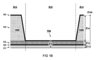
図1Aは、隣接する音響変換器10a、10bの断面図を図示し、図1Bは、変換器10aのうちの1つのさらなる詳細を図示する。
Figure 1A illustrates a cross-sectional view of adjacent
好ましい実施形態では、たとえば示されるように、音響デバイス100は、音響変換器10a、10bのアレイを備える。別の実施形態またはさらなる実施形態では、アレイは、フレキシブル基板11上のパターン形成したスタック12~15によって形成される。いくつかの実施形態では、スタックは、それぞれの底部電極層12と上部電極層15との間に挟まれる圧電層13を備える。他の実施形態またはさらなる実施形態では、スタックは、絶縁層14を備える。好ましくは、絶縁層14はパターン形成される。たとえば、パターン形成した絶縁層14は、絶縁材料14mのパターンによって形成される。
In a preferred embodiment, for example as shown, the
好ましい実施形態では、たとえば示されるように、パターン形成した絶縁層(14)は、絶縁材料14mが電極12、15のうちの1つと圧電層13の間に(基板11を横断する方向Zに)配設される絶縁区域A14を備える。別のまたはさらなる好ましい実施形態では、パターン形成した絶縁層(14)は、両方の電極12、15が圧電層13と接触する、絶縁材料14mがない接触区域A10を備える。より好ましくは、音響変換器10a、10bが接触区域A10に形成される。たとえば、音響変換器10a、10bは絶縁区域A14の間に形成される。最も好ましくは、絶縁区域A14が、それぞれの接触区域A10を囲む、および/または分離する。言い換えると、絶縁材料14mのパターンは、音響変換器10a、10bの周りに境界を規定することができ、ここで、接触区域A10は、圧電層13と電極12、15のいずれかとの間で絶縁材料14mなしにパターン中の間隙に形成される。
In a preferred embodiment, for example as shown, the patterned insulating layer (14) comprises insulating areas A14 where the insulating
好ましい実施形態では、たとえば示されるように、音響変換器10a、10bの作動面は、接触区域A10においてフレキシブル基板11の部分を含む。言い換えると、それぞれの音響変換器10aは、フレキシブル基板11を備えるスタックによって形成することができ、圧電層13は、それぞれの底部電極層12と上部電極層15との間に挟まれるが、絶縁材料14mはその区域すなわち接触区域A10にはない。
In a preferred embodiment, for example as shown, the working surface of the
好ましくは、基板11は、たとえば、意図されるような音響波Wを生成するため圧電層13を曲げるまたは撓曲するのに少なくとも十分な比較的高い可撓性を有する。典型的には、基板11の(スタックなしでそれ自体の)第1の屈曲剛性は、変換器の部分として(すなわち、絶縁材料14mを除く)、基板11上に設けられる層のスタックの第2の屈曲剛性と同じ程度であってよい。たとえば、第1の屈曲剛性は、第2の屈曲剛性の0.1倍~10倍の間である。代わりにまたは追加で、このことは、(基板の)(第1の)屈曲剛性は、接触区域A10において、デバイスの全屈曲剛性Fa、すなわち、第1の屈曲剛性と第2の屈曲剛性の合計の90パーセント未満を構成すると定量化することができる。
Preferably, the
好ましい実施形態では、基板11を取り除く必要はなく、音響デバイス100の部分のままとすることができる。別の実施形態(図示せず)では、スタックは、スタックが製造され、フレキシブル基板または別の支持基板であってよい基板から取り除くことができる。たとえば、パターン形成した絶縁材料14mは、基板なしでデバイスを支持するのに十分な構造的完全性を実現することができる。このことによって、構成が製造期間に固定されたままにするために、たとえば比較的剛性の基板を使用することも可能にすることができる。
In a preferred embodiment, the
好ましい実施形態では、音響デバイス100は、比較的平坦であり、たとえばシートとして形成される。そのため、好ましくは、音響デバイス100の平面を横断する方向の合計の厚さZ100は、その(最小)面内寸法(直径または長さ/幅)の程度と比べて比較的小さい。たとえば、面内寸法は、少なくとも10倍、20倍、50倍、100倍、1000倍、またはそれ以上だけ厚さより大きい。たとえば、基板11、電極12、15を有する圧電層13、および絶縁区域A14の合計の厚さ(Z100)は、1ミリメートル未満、0.5ミリメートル未満、たとえば、100マイクロメートルと200マイクロメートルの間であってよい。
In a preferred embodiment, the
音響変換器10a、10b間のたとえば面内波Wiといったクロストークを効果的に緩和するために、音響変換器それぞれの振動を減結合するおよび/または減衰させることが望ましい。たとえば、減結合は、異なる波伝播特性を有する変換器を、変換器を形成する区域から分離する基板の区域を設けることによって、達成することができる。たとえば、減衰は、変換器間の区域に、より多くのおよび/または異なる(たとえば、消散的な)タイプの材料を設けることによって達成することができる。
To effectively mitigate crosstalk, e.g., in-plane waves Wi, between
比較的平坦な音響デバイス100の異なる区域を特徴づける1つの方法は、音響デバイス100それぞれの屈曲剛性(F)または曲げ剛性によるものである。たとえば、層またはスタックの屈曲剛性(F)は、そのヤング率(E)、ポアソン比(v)、および厚さ(Z)に依存することができる。典型的には、これは、F=[E・Z3]/[12・(1-v2)]と書くことができる。好ましい実施形態では、絶縁層14を含む絶縁区域A14における屈曲剛性Fxは、音響変換器10a、10bを形成する接触区域A10における屈曲剛性Faよりも、少なくとも10倍、より好ましくは少なくとも20倍、最も好ましくは少なくとも50倍、たとえば60倍と200倍の間だけ高い。絶縁区域の相対的な屈曲剛性が高くなると、隣接する変換器間の面内クロストークをより緩和することができる。
One way to characterize the different sections of the relatively flat
絶縁区域A14の比較的高い屈曲剛性は、たとえばフレキシブル基板11のヤング率より高い、比較的高いヤング率を有する絶縁材料14mを使用することによって実現することができる。代わりにまたは追加で、絶縁材料14mの層の厚さZ14が比較的厚くてよい。好ましい実施形態では、絶縁区域A14は、接触区域A10と比較して、スタックに対して局所的に増やした厚さZ14を実現する。たとえば、絶縁区域A14におけるスタックの厚さZ100(たとえば、Z11+Z13+Z14に等しい)は、接触区域A10におけるスタックの厚さZ10(たとえば、Z11+Z13に等しい)よりも、少なくとも2倍、好ましくは少なくとも3倍だけ厚い。
The relatively high bending stiffness of the insulating area A14 can be achieved by using an insulating
例示的な製造したデバイスでは、基板11は、厚さZ11=13.5μmを有するポリイミド(PI)基板によって形成された。基板上に、厚さZ13=20μmを有するPVDFスタックによって、圧電層13が形成された。区域A10(すなわち、基板+圧電層)におけるデバイス100の屈曲剛性は、Fa=1.35E-5N・m(=Pa・m3)で推定される。絶縁区域A14において、上部電極15を付加する前に、絶縁材料14mの追加の層が堆積された。具体的には、厚さZ14=125μmを有するフォトレジストの層(SU8)によって絶縁材料14mが形成された。この追加の層を含めて、区域A14におけるデバイス100の屈曲剛性は、Fi=1.19E-3N・mで推定され、すなわち、区域A10より88倍高い。
In the exemplary manufactured device, the
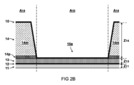
図2Aは、絶縁材料14mが底部電極12と圧電層13との間に付加される音響デバイス100の断面図を図示する。これは、たとえば、絶縁材料14mが圧電層13と上部電極15の間に付加される、図1Aおよび図1Bの実施形態と対照的である。好ましい実施形態では、絶縁材料は、フォトレジスト材料から形成される。そのような材料によって、製造性をさらに改善することができ、たとえば、フォトレジストを現像するための対応する光パターン/マスクによって、絶縁材料14mのパターンを規定する簡単な方法が実現される。いくつかの実施形態では、絶縁材料14mのパターン形成が圧電層13に影響を及ぼす可能性があることを想定することができる。たとえば、フォトレジスト材料、および/または、ウェットエッチングなどのプロセスによって、接触区域A10において、フォトレジストを(選択的に)除去する方法。いくつかの実施形態では、たとえば示されるように、これは、圧電層13の前に絶縁材料14mを付加することによって緩和することができる。
2A illustrates a cross-sectional view of an
図2Bは、中間保護層14pを有する音響デバイス100の断面図を図示する。いくつかの実施形態では、中間保護層14pは、圧電層13と絶縁材料14mとの間に配設される。中間保護層14pは、代わりにまたは追加で、たとえば示される絶縁材料14m(フォトレジスト)および/またはその除去方法に露出することから圧電層13を保護するために使用することができる。このようにして、圧電層13は、絶縁材料14mの層のパターン形成の前に、やはり付加することができる。典型的には、保護層14pは、絶縁材料14mとは異なる材料を有することができる。たとえば、保護層14pは、絶縁材料14mを除去するためのエッチングプロセスに対して、より耐性があってよい。好ましくは、中間保護層14pは、その後、たとえばドライエッチング(ガス)などといった(フォトレジストを除去するために使用されたものと)別のプロセスを使用して、接触区域A10において、局所的に除去される。原理的に、保護層14pは、絶縁材料14mに加えて、電極と圧電層それぞれの間の電気絶縁体の部分として、および/または、隣接する変換器間の音響絶縁体の部分として働くことができる。その意味で、両方の層14mおよび14pは、パターン形成した絶縁材料の部分と考えることができる。
2B illustrates a cross-sectional view of the
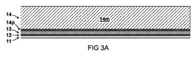
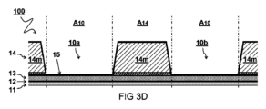
図3A~図3Dは、音響デバイス100を製造する方法を図示する。
Figures 3A-3D illustrate a method for manufacturing
一実施形態では、たとえば図3Aに示されるように、方法は、フレキシブル基板11上に形成されるスタックを設けるステップを含む。好ましくは、スタックは(最初に)少なくとも底部電極12を備える。いくつかの実施形態では、たとえば図3Aおよび図3Bに示されるように、絶縁材料14mの層がスタック上に堆積され、選択的に除去される。絶縁材料14mが除去される場所は、スタックを通して底部電極12と電気的に接触するための接触区域A10を形成することになる。堆積後に材料を除去するステップの代わりに、たとえば開口部を有する箔といった、予めパターン形成した絶縁材料の層を、スタックに付加することができる(たとえば、図7Aに示される)。
In one embodiment, the method includes providing a stack formed on a
いくつかの実施形態では、たとえば図3Dに示されるように、スタック上の上部電極15は、接触区域A10に音響変換器10a、10bのアレイを形成し、そこでは、上部電極と底部電極の両方がそれらの間で圧電層13と接触し、その圧電層13は、絶縁材料14mの層を堆積するステップの前または後にスタック上に堆積され、音響変換器10a、10bが絶縁区域A14によって分離され、絶縁材料14mが、電極12、15および圧電層13のうちの1つの間に配設される。
In some embodiments, as shown, for example, in FIG. 3D, the
いくつかの実施形態では、絶縁材料14mは、フォトレジスト材料を含む。他の実施形態またはさらなる実施形態では、パターン形成した絶縁層14は、リソグラフィックプロセスによって形成される。たとえば、絶縁材料14mのパターン形成してない層が、接触区域A10の形状または絶縁区域A14の形状と一致する光のパターンにさらされる。たとえば、パターン形成した露光を実現するためにマスクが使用される。たとえば比較的小さい寸法および/または多くの個数で、音響変換器の所望の高い精度のパターンを容易に形成するために、リソグラフを使用できることが理解されよう。
In some embodiments, the insulating
いくつかの実施形態では、たとえば図3Aに示されるように、保護層14pが、圧電層13と絶縁層14の間に設けられる。たとえば、図3Bに示されるように、たとえばウェットエッチングといった、絶縁層14をパターン形成するための除去プロセスに対して、圧電層13を保護するために、絶縁材料14mを除去するときに保護層14pが残ることができる。いくつかの実施形態では、たとえば図3Cに示されるように、保護層14pは、たとえばドライエッチングといった別個のプロセスによって、接触区域A10で除去することができる。したがって、たとえば図3Dに示されるように、上部電極層15は、それらの間の保護層14pなしで、圧電層13上に堆積することができる。
In some embodiments, a
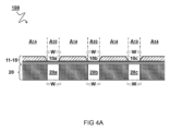
図4Aおよび図4Bは、支持構造20に固定されるフレキシブル基板11を有する音響デバイス100を図示する。
Figures 4A and 4B illustrate an
いくつかの実施形態では、たとえば示されるように、フレキシブル基板11は、比較的剛性の支持基板20上に固定される、たとえば積層される、さもなければ配設される。たとえば、基板11は、積層すること、および/さもなければ、支持基板20に付着させることができる。フレキシブル基板と支持基板または他の剛性構造との間の固定は、たとえば製造期間および/または製造後に行うことができる。支持基板は、フレキシブル基板11と同様に比較的平坦であってよく、またはフレキシブル基板11と比較してより厚くてよい。好ましくは、支持基板20は、フレキシブル基板11と比べて、たとえば少なくとも2倍、3倍、5倍、10倍、またはそれ以上といった比較的高い屈曲剛性を有する。したがって、支持基板20は、追加の構造的完全性を実現することができる。
In some embodiments, for example as shown, the
好ましくは、支持基板20は、音響変換器10a~10cに対応する位置に、すなわち少なくとも部分的に接触区域A10と重なり合う開口部20a~20cを備える。たとえば、フレキシブル基板11が絶縁区域A14で支持構造に突き当たる一方で、接触区域A10では支持構造20に接続しない。いくつかの実施形態では、開口部20a~20cは、たとえば図4Aに示されるように、支持基板20を通って延びることができる。他の実施形態またはさらなる実施形態では、開口部20a~20cは、フレキシブル基板11の方向から凹面状に延びるが、支持基板20を完全には貫通しない空洞によって形成することができる。開口部は、変換面の比較的自由な運動を可能にする一方で、依然として剛性の支持を実現することができる。追加で、支持構造への絶縁区域A14の固定によって、変換器10a、10b間になお一層の音響的絶縁を実現するのを助けることができる。いくつかの実施形態(図示せず)では、支持基板は、たとえばスタックを堆積して完成させた後で、上側に設けることができる。また、音響波Wを伝送するため少なくとも片側に、好ましくは図4Aに示されるものなどといった貫通開口部を有する、片側または両側の支持構造との組合せも可能である。
Preferably, the
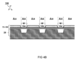
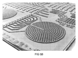
図5Aは、例示的なレイアウトによる変換器のアレイを図示する。図5Bは、同様のレイアウトを有するデバイスの写真を示す。 Figure 5A illustrates an array of transducers with an example layout. Figure 5B shows a photograph of a device with a similar layout.
いくつかの実施形態では、たとえば示されるように、変換器の中心は、複数の同心円に沿って配置することができる。したがって、それぞれの円に沿った変換器の各々は、デバイスの平面を横断する方向の、円の中心軸に沿った点に対して同じ距離を有することができる。それぞれの第1の円に沿った変換器の第1の組を同相で作動させることによって、それらの変換器の音響波は、中心軸に沿った点で強め合うように干渉することができる。それぞれの第2の円に沿った変換器の第2の組を第1の組内でやはり同相で、だが第1の組に対して予め規定された位相差で追加で作動させることによって、組の間で強め合う干渉が生じる特定の点を、デバイスの面の上方で選択することができる。これは、追加の組によってさらに改善することができる。一実施形態では、示されるデバイスは、多くの変換器間で強め合う干渉によって、空中に触知できる点を作る、触覚フィードバックデバイスを作成するために使用することができる。たとえば、点の場所は、(中心軸に沿って)変換器の組の間の、または(点を軸外に動かすため)それぞれの組内の相対的な位相を制御することによって制御することができる。もちろん、たとえば格子状レイアウトといった他のレイアウトも、同様または他の音響デバイスを作るために使用することができる。 In some embodiments, the centers of the transducers can be arranged along multiple concentric circles, for example as shown. Thus, each of the transducers along each circle can have the same distance to a point along the central axis of the circle in a direction transverse to the plane of the device. By activating a first set of transducers along each first circle in phase, their acoustic waves can constructively interfere at a point along the central axis. By additionally activating a second set of transducers along each second circle, also in phase within the first set but with a predefined phase difference relative to the first set, a specific point can be selected above the face of the device where constructive interference between the sets occurs. This can be further improved with additional sets. In one embodiment, the device shown can be used to create a tactile feedback device that creates a tactile dot in the air by constructive interference between many transducers. For example, the location of the dot can be controlled by controlling the relative phase between the sets of transducers (along the central axis) or within each set (to move the dot off-axis). Of course, other layouts, for example a grid layout, can be used to create similar or other acoustic devices.
本明細書に記載されるような効果的な減結合によって、任意のレイアウトにおける、隣接する変換器10a、10b間の横方向間隔または距離Xabは比較的小さく、たとえば、変換器10a、10bの(最大または平均の)直径Xa、Xbと同じ程度であってよいことを理解されよう。たとえば、変換器間の(最小)距離Xabは、変換器の(一定または平均)直径Xa、Xbの0.1倍~10倍の間であって、好ましくは0.2倍~5倍の間、より好ましくは半分から2倍の間である。いくつかの実施形態では、デバイスの面にわたる変換器の密度が比較的高くてよく、たとえば、変換器は、面(変換器間の区域によって形成される残りの面)の少なくとも10パーセント、好ましくは少なくとも20パーセント、より好ましくは少なくとも30パーセント、または50パーセントすら超えてカバーすることができる。変換器によってより広い面をカバーすることができると、デバイスの動作はより効果的になることができる。
It will be appreciated that with effective decoupling as described herein, the lateral spacing or distance Xab between
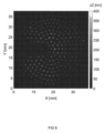
図6は、変換器が作動される場合の、図5Bに示されたような音響デバイスの表面X、YにわたるたわみΔZの測定を(ナノメートル単位で)図示する。測定は、レーザ振動計を使用して実施された。図示されるように、たわみΔZが、変換器の接触区域に限定される一方で、変換器間の絶縁区域には事実上目立つたわみがなく、たとえば、絶縁区域におけるたわみは、接触区域におけるたわみよりも少なくとも1/10未満である。 Figure 6 illustrates the measurement of deflection ΔZ (in nanometers) across the surface X, Y of an acoustic device as shown in Figure 5B when the transducer is actuated. The measurement was performed using a laser vibrometer. As shown, the deflection ΔZ is confined to the contact area of the transducers, while there is virtually no noticeable deflection in the insulating area between the transducers, e.g., the deflection in the insulating area is at least 1/10th less than the deflection in the contact area.
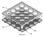
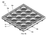
図7Aおよび図7Bは、音響変換器10a、10bの別のレイアウトを図示する。一実施形態では、たとえば図7Aに示されるように、絶縁層14は、スタックに付加される前に予めパターン形成される。あるいは、図7Bに示される絶縁層14は、たとえば図3A~図3Dを参照して記載されたように、材料の選択的除去によってパターン形成することができる。
Figures 7A and 7B illustrate alternative layouts of
好ましい実施形態では、圧電層13は、異なる変換器10a、10b間に延びる連続した層である。有利なことに、圧電材料を連続した層として堆積するのは、はるかに容易な場合がある。好ましくは、ポリマベースの圧電材料が圧電層13用に使用される。たとえば、ポリマベースの圧電材料は、連続した層として容易に付加することができる。いくつかの実施形態では、堆積した圧電材料は、最初に、ランダムに配向される領域を有する場合がある。好ましくは、これらは、圧電材料を「極性化すること」、すなわち、通常は高い温度で、材料にわたって強い電場が印可されるプロセスによって整列される。最も好ましくは、圧電層13は、接触区域A10においてもっぱら(または主に)極性化される。たとえば、極性化のための強い電場は、底部電極12および上部電極(ここでは、見ることができない)を介して印可される。パターン形成した絶縁層14に起因して、電極間の電位差によって、絶縁区域A14のより大きい間隙の両端間のものより強い、接触区域A10における圧電層13の両端間の電場をもたらすことができる。認識されるように、選択的な極性化は、機能性を改善すること、たとえば、絶縁区域A14の非極性化領域における圧電層13の作動をさらに防ぐことを助けることもできる。
In a preferred embodiment, the
いくつかの実施形態では、底部電極と上部電極のうちの少なくとも1つは、異なる変換器10a、10b間に延びる連続した層である。他の実施形態またはさらなる実施形態では、電極12、15のうちの少なくとも1つは、パターン形成される。一実施形態では、パターン形成した電極層とパターン形成しない電極層の組合せが使用される。好ましくは、電極のパターン形成は、音響変換器10a、10bのうちの1つまたは複数のサブセットを選択的に作動できるようなものである。一実施形態では、1つまたは複数の変換器10aの第1の組が、底部電極の第1のライン12aに電圧を印加することによって作動され、異なる1つまたは複数の変換器10bの第2の組が、異なる底部電極の第2のライン12aに電圧を印加することによって作動される。いくつかの実施形態では、たとえば示されるように、ライン12a、12bが、少なくとも接触区域A10をカバーするように形作られる接触パッドを備えることができる。パターン形成される底部電極の代わりにまたは追加で、上部電極をパターン形成することができる(図示せず)。いくつかの実施形態(図示せず)では、上部電極のパターンは、たとえば、垂直な格子線を形成して底部電極のパターンを補完することができる。他の実施形態またはさらなる実施形態では、たとえば示されるように、電極ラインの格子を、圧電層13の片側に形成することができる。たとえば、格子は、薄膜トランジスタ(TFT)を備えることができる。
In some embodiments, at least one of the bottom and top electrodes is a continuous layer extending between the
分かりやすく簡潔な記載にするために、特徴は、本明細書では、同じまたは別個の実施形態の部分として記載されるが、本発明の範囲は、記載される特徴の全部または一部の組合せを有する実施形態を含むことができることを理解されよう。たとえば、実施形態が特定の順序の層について示される一方で、同様の機能および結果を達成するために、本開示の利益を有する当業者によって、また代替方法が想定される可能性がある。たとえば、いくつかの層は組み合わせること、または、1つもしくは複数の代替層へと分割することができる。議論され示される本実施形態の様々な要素は、横方向の振動を分離することなどといったある種の利点を提供する。もちろん、考案および利点を発見して整合させる際に、上の実施形態またはプロセスのうちの任意の1つを1つまたは複数の他の実施形態またはプロセスと組み合わせて、またさらなる改善を実現することができることを理解されたい。本開示は、音響変換器アレイに対して特段の利益を提供し、一般的に、絶縁層が電極層を選択的に分離することによって形成される選択的接触区域間に他の電気構成要素を形成するために適用することができることが理解されよう。 For clarity and conciseness of description, features are described herein as part of the same or separate embodiments, but it will be understood that the scope of the present invention can include embodiments having all or a combination of the described features. For example, while an embodiment is shown with a particular order of layers, alternative methods may also be envisioned by one skilled in the art having the benefit of this disclosure to achieve similar functions and results. For example, some layers can be combined or split into one or more alternative layers. The various elements of the present embodiment discussed and shown provide certain advantages, such as isolating lateral vibrations. Of course, in discovering and matching ideas and advantages, it will be understood that any one of the above embodiments or processes can be combined with one or more other embodiments or processes to achieve further improvements. It will be understood that the present disclosure provides particular benefits for acoustic transducer arrays and can be generally applied to form other electrical components between selective contact areas formed by insulating layers selectively isolating electrode layers.
添付の特許請求の範囲を解釈する際に、「備える(comprising)」という言葉は、他の要素の存在を除外しないことまたは所与の請求項中でリスト化されるもの以外の働きをすること、要素の前の「a」または「an」という言葉は、複数のそのような要素の存在を除外しないこと、請求項中の何らかの参照符号は請求の範囲を制限しないこと、いくつかの「手段」は、同じもしくは異なる項目または実装される構造もしくは機能によって表すことができること、開示されるデバイスまたはそれらの部分のいずれかは、別段の指定がなければ、一緒に組み合わせることまたはさらなる部分へと分割することができることを理解されたい。1つの請求項が別の請求項を参照する場合、これは、それらそれぞれの特徴の組合せによって達成される共同作用の利点を示すことができる。しかし、ある処置が相互に異なる請求項で言及されるという単なる事実は、これらの処置の組合せをやはり効果的に使用できないとは示していない。本実施形態は、こうして、請求項のすべての作用する組合せを含むことができ、各請求項は、原理的に、文脈によって明瞭に除外されない限り、任意の前の請求項を参照することができる。 In interpreting the appended claims, it should be understood that the word "comprising" does not exclude the presence of other elements or acts other than those listed in a given claim, the word "a" or "an" before an element does not exclude the presence of a plurality of such elements, any reference sign in a claim does not limit the scope of the claim, several "means" can be represented by the same or different items or structures or functions implemented, any of the disclosed devices or parts thereof can be combined together or divided into further parts unless otherwise specified. When one claim refers to another claim, this can indicate the advantage of a synergy achieved by the combination of their respective features. However, the mere fact that certain measures are mentioned in mutually different claims does not indicate that a combination of these measures cannot also be used to advantage. The present embodiment can thus include all operative combinations of the claims, and each claim can in principle refer to any previous claim unless clearly excluded by the context.
10a 音響変換器
10b 音響変換器
10c 音響変換器
11 フレキシブル基板
12 スタック、底部電極層
12a 第1のライン、第2のライン
12b ライン
13 スタック、圧電層
14 スタック、絶縁層
14m 絶縁材料
14p 中間保護層
15 スタック、上部電極層
20 支持構造、支持基板
20a 開口部
20b 開口部
20c 開口部
100 音響デバイス
A10 接触区域
A14 絶縁区域
Fa 屈曲剛性
Fx 屈曲剛性
W 音響波
X 表面
Xa 直径
Xb 直径
Xab 距離
Y 表面
Z10 スタックの厚さ
Z11 厚さ
Z13 厚さ
Z14 厚さ
Z100 スタックの厚さ
ΔZ たわみ
Claims (15)
異なる変換器(10a、10b)間に延び、それぞれの底部電極層(12)と上部電極層(15)との間に挟まれる連続した圧電層(13)と、
絶縁材料(14m)のパターンによって形成されるパターン形成した絶縁層(14)と
を備え、前記パターンが、
前記絶縁材料(14m)が前記電極(12、15)のうちの1つと前記圧電層(13)との間に配設される絶縁区域(A14)と、
両方の電極(12、15)が前記圧電層(13)と接触する、前記絶縁材料(14m)がない接触区域(A10)と
を備える、音響デバイス(100)。 An acoustic device (100) comprising an array of acoustic transducers (10a, 10b) formed by a patterned stack (12-15) on a flexible substrate (11), said stack comprising:
a continuous piezoelectric layer (13) extending between the different transducers (10a, 10b) and sandwiched between respective bottom electrode layers (12) and top electrode layers (15);
a patterned insulating layer (14) formed by a pattern of insulating material (14m), said pattern comprising:
an insulating area (A14) in which the insulating material (14m) is disposed between one of the electrodes (12, 15) and the piezoelectric layer (13);
and a contact area (A10) free of said insulating material (14m), where both electrodes (12, 15) are in contact with said piezoelectric layer (13).
フレキシブル基板(11)上に形成されるスタックを設けるステップであって、前記スタックが、少なくとも底部電極(12)を備える、ステップと、
前記スタック上に絶縁材料(14m)の層を堆積し、前記スタックを通して前記底部電極(12)と電気的に接触するための接触区域(A10)を形成するために前記絶縁材料(14m)を選択的に除去するステップと、
前記接触区域(A10)に音響変換器(10a、10b)のアレイを形成するため前記スタック上に上部電極(15)を堆積するステップであって、前記上部電極と前記底部電極の両方が、それらの間で圧電層(13)と接触し、前記圧電層(13)が、前記絶縁材料(14m)の層を堆積する前記ステップの前または後に前記スタック上に堆積され、前記音響変換器(10a、10b)が、絶縁区域(A14)によって分離され、前記絶縁材料(14m)が、前記電極(12、15)のうちの1つと前記圧電層(13)との間に配設され、前記圧電層(13)が、異なる変換器(10a、10b)間に延びる連続した層である、ステップと
を含む、方法。 A method of manufacturing an acoustic device (100), comprising the steps of:
Providing a stack formed on a flexible substrate (11), said stack comprising at least a bottom electrode (12);
depositing a layer of insulating material (14m) on said stack and selectively removing said insulating material (14m) to form contact areas (A10) for making electrical contact with said bottom electrode (12) through said stack;
depositing a top electrode (15) on the stack to form an array of acoustic transducers (10a, 10b) in the contact area (A10), both the top electrode and the bottom electrode being in contact with a piezoelectric layer (13) between them, the piezoelectric layer (13) being deposited on the stack before or after the step of depositing the layer of insulating material (14m), the acoustic transducers (10a, 10b) being separated by insulating areas (A14), the insulating material (14m) being disposed between one of the electrodes (12, 15) and the piezoelectric layer (13), the piezoelectric layer (13) being a continuous layer extending between the different transducers (10a, 10b).
Applications Claiming Priority (3)
| Application Number | Priority Date | Filing Date | Title |
|---|---|---|---|
| EP19171943.4A EP3733310A1 (en) | 2019-04-30 | 2019-04-30 | Acoustic piezoelectric membrane transducer arrays with localized membrane vibrations |
| EP19171943.4 | 2019-04-30 | ||
| PCT/NL2020/050265 WO2020222639A1 (en) | 2019-04-30 | 2020-04-29 | Acoustic piezoelectric membrane transducer arrays with localized membrane vibrations |
Publications (2)
| Publication Number | Publication Date |
|---|---|
| JP2022530663A JP2022530663A (en) | 2022-06-30 |
| JP7641237B2 true JP7641237B2 (en) | 2025-03-06 |
Family
ID=66349354
Family Applications (1)
| Application Number | Title | Priority Date | Filing Date |
|---|---|---|---|
| JP2021564578A Active JP7641237B2 (en) | 2019-04-30 | 2020-04-29 | Acoustic piezoelectric membrane transducer array with localized membrane vibrations. |
Country Status (5)
| Country | Link |
|---|---|
| US (1) | US20220193723A1 (en) |
| EP (2) | EP3733310A1 (en) |
| JP (1) | JP7641237B2 (en) |
| CN (1) | CN113766977A (en) |
| WO (1) | WO2020222639A1 (en) |
Families Citing this family (6)
| Publication number | Priority date | Publication date | Assignee | Title |
|---|---|---|---|---|
| FR3116630B1 (en) * | 2020-11-26 | 2023-06-02 | Commissariat A L’Energie Atomique Et Aux Energies Alternatives | Haptic interface |
| EP4016074A1 (en) * | 2020-12-18 | 2022-06-22 | Universite De Franche-Comte | Acoustic biosensor assay assembly |
| WO2022141585A1 (en) * | 2020-12-31 | 2022-07-07 | 深圳市韶音科技有限公司 | Bone conduction-based sound conduction device |
| US11843915B2 (en) * | 2021-08-20 | 2023-12-12 | Massachusetts Institute Of Technology | Active piezoelectric sheet with piezoelectric microstructures |
| CN115148893B (en) * | 2022-07-28 | 2025-09-19 | 西安交通大学 | Flexible PMUTs with bending and torsional deformation functions and preparation method thereof |
| CN117750285B (en) * | 2024-02-07 | 2024-05-07 | 山东博华电子科技发展有限公司 | Preparation method of miniature piezoelectric transducer and miniature piezoelectric transducer |
Citations (4)
| Publication number | Priority date | Publication date | Assignee | Title |
|---|---|---|---|---|
| JP2002027594A (en) | 2000-07-11 | 2002-01-25 | Hitachi Ltd | Ultrasonic probe and manufacturing method thereof |
| JP2006333121A (en) | 2005-05-26 | 2006-12-07 | Mitsubishi Electric Engineering Co Ltd | Super-directivity speaker |
| JP2009139339A (en) | 2007-12-10 | 2009-06-25 | Seiko Epson Corp | SEMICONDUCTOR PRESSURE SENSOR AND ITS MANUFACTURING METHOD, SEMICONDUCTOR DEVICE, AND ELECTRONIC DEVICE |
| JP2012503370A (en) | 2008-09-18 | 2012-02-02 | ビジュアルソニックス インコーポレイテッド | Ultrasonic transducer and other component manufacturing method |
Family Cites Families (16)
| Publication number | Priority date | Publication date | Assignee | Title |
|---|---|---|---|---|
| JPS555570A (en) * | 1978-06-28 | 1980-01-16 | Furuno Electric Co Ltd | Ultrasonic wave reception unit |
| GB9108490D0 (en) * | 1991-04-20 | 1991-06-05 | Jones Richard W | Device for acoustic wave generation |
| EP1769759B1 (en) * | 1999-05-11 | 2008-08-13 | Atrionix, Inc. | Apparatus for ultrasound ablation |
| JP2008072482A (en) * | 2006-09-14 | 2008-03-27 | Mitsubishi Electric Engineering Co Ltd | Speaker device |
| DE102008029378B4 (en) * | 2008-06-20 | 2010-04-15 | Siemens Aktiengesellschaft | Arrangement of a piezoacoustic resonator on an acoustic mirror of a substrate, method for producing the arrangement and use of the arrangement |
| US9173047B2 (en) * | 2008-09-18 | 2015-10-27 | Fujifilm Sonosite, Inc. | Methods for manufacturing ultrasound transducers and other components |
| CN101712028B (en) * | 2009-11-13 | 2012-02-01 | 中国科学院声学研究所 | A kind of thin film ultrasonic transducer and its preparation method |
| WO2012107388A1 (en) * | 2011-02-07 | 2012-08-16 | Deutsches Zentrum für Luft- und Raumfahrt e.V. | Transparent acoustically active device |
| US9061320B2 (en) | 2012-05-01 | 2015-06-23 | Fujifilm Dimatix, Inc. | Ultra wide bandwidth piezoelectric transducer arrays |
| US8969170B2 (en) * | 2013-03-14 | 2015-03-03 | Globalfoundries Inc. | Method of forming a semiconductor structure including a metal-insulator-metal capacitor |
| CN103240220B (en) * | 2013-05-09 | 2015-06-17 | 电子科技大学 | Piezoelectric array ultrasonic transducer |
| US9604255B2 (en) * | 2014-01-10 | 2017-03-28 | Fujifilm Dimatix, Inc. | Method, apparatus and system for a transferable micromachined piezoelectric transducer array |
| JP6606866B2 (en) * | 2015-05-29 | 2019-11-20 | セイコーエプソン株式会社 | Piezoelectric device and probe, electronic apparatus and ultrasonic imaging apparatus |
| EP3703874B1 (en) * | 2017-10-31 | 2022-05-18 | Koninklijke Philips N.V. | Ultrasound scanner assembly |
| WO2020131020A1 (en) * | 2018-12-17 | 2020-06-25 | Emerge Now Inc. | Systems for interfacing with immersive computing environments |
| US11950512B2 (en) * | 2020-03-23 | 2024-04-02 | Apple Inc. | Thin-film acoustic imaging system for imaging through an exterior surface of an electronic device housing |
-
2019
- 2019-04-30 EP EP19171943.4A patent/EP3733310A1/en not_active Withdrawn
-
2020
- 2020-04-29 CN CN202080032588.2A patent/CN113766977A/en active Pending
- 2020-04-29 EP EP20723223.2A patent/EP3962665B1/en active Active
- 2020-04-29 WO PCT/NL2020/050265 patent/WO2020222639A1/en not_active Ceased
- 2020-04-29 JP JP2021564578A patent/JP7641237B2/en active Active
- 2020-04-29 US US17/605,437 patent/US20220193723A1/en active Pending
Patent Citations (4)
| Publication number | Priority date | Publication date | Assignee | Title |
|---|---|---|---|---|
| JP2002027594A (en) | 2000-07-11 | 2002-01-25 | Hitachi Ltd | Ultrasonic probe and manufacturing method thereof |
| JP2006333121A (en) | 2005-05-26 | 2006-12-07 | Mitsubishi Electric Engineering Co Ltd | Super-directivity speaker |
| JP2009139339A (en) | 2007-12-10 | 2009-06-25 | Seiko Epson Corp | SEMICONDUCTOR PRESSURE SENSOR AND ITS MANUFACTURING METHOD, SEMICONDUCTOR DEVICE, AND ELECTRONIC DEVICE |
| JP2012503370A (en) | 2008-09-18 | 2012-02-02 | ビジュアルソニックス インコーポレイテッド | Ultrasonic transducer and other component manufacturing method |
Also Published As
| Publication number | Publication date |
|---|---|
| EP3733310A1 (en) | 2020-11-04 |
| US20220193723A1 (en) | 2022-06-23 |
| CN113766977A (en) | 2021-12-07 |
| EP3962665B1 (en) | 2024-10-09 |
| EP3962665A1 (en) | 2022-03-09 |
| EP3962665C0 (en) | 2024-10-09 |
| JP2022530663A (en) | 2022-06-30 |
| WO2020222639A1 (en) | 2020-11-05 |
Similar Documents
| Publication | Publication Date | Title |
|---|---|---|
| JP7641237B2 (en) | Acoustic piezoelectric membrane transducer array with localized membrane vibrations. | |
| JP5144875B2 (en) | Alignment method for the manufacture of integrated ultrasonic transducer arrays | |
| CN103121657B (en) | MEMS and manufacture method thereof | |
| JP7609780B2 (en) | Piezoelectric element | |
| US10081533B2 (en) | Micromechanical structure and method for fabricating the same | |
| US20050046030A1 (en) | Laminated structure, method of manufacturing the same and ultrasonic transducer array | |
| TW200826717A (en) | Electrostatic pressure transducer and manufacturing method therefor | |
| US6168906B1 (en) | Micromachined membrane with locally compliant and stiff regions and method of making same | |
| WO2016047186A1 (en) | Ultrasonic transducer, method for making same, ultrasonic transducer array, and ultrasonic test apparatus | |
| KR20180031744A (en) | DSR speaker element and its manufacturing method | |
| JP2019114958A (en) | Electro-acoustic transducer | |
| JP7215802B2 (en) | Processes for designing and manufacturing devices containing arrays of micromachined elements, devices obtained at the end of such processes | |
| JP7576084B2 (en) | Optimization of acoustic membrane arrays. | |
| JP2009198493A (en) | Angular velocity detection device | |
| JP2008028513A (en) | Capacitor microphone and manufacturing method therefor | |
| JP7768043B2 (en) | MEMS transducer | |
| JP7754393B2 (en) | Sound generating cell, acoustic transducer, and method for manufacturing a sound generating cell | |
| JP7526654B2 (en) | Sonic speaker | |
| JP2025073733A (en) | Electroacoustic Transducer | |
| JP2012165308A (en) | Ultrasonic transducer | |
| JP2024158341A (en) | Vibration device, speaker unit, and method for manufacturing vibration device | |
| JP7226683B2 (en) | Manufacturing method of MEMS element | |
| CN119855657A (en) | Acoustic device and method of manufacture | |
| Zhang et al. | CMUTs with interlaced high-and low-frequency elements | |
| CN117812509A (en) | Directional MEMS speaker array and manufacturing method |
Legal Events
| Date | Code | Title | Description |
|---|---|---|---|
| A621 | Written request for application examination |
Free format text: JAPANESE INTERMEDIATE CODE: A621 Effective date: 20230405 |
|
| A977 | Report on retrieval |
Free format text: JAPANESE INTERMEDIATE CODE: A971007 Effective date: 20240424 |
|
| A131 | Notification of reasons for refusal |
Free format text: JAPANESE INTERMEDIATE CODE: A131 Effective date: 20240513 |
|
| A601 | Written request for extension of time |
Free format text: JAPANESE INTERMEDIATE CODE: A601 Effective date: 20240809 |
|
| TRDD | Decision of grant or rejection written | ||
| A01 | Written decision to grant a patent or to grant a registration (utility model) |
Free format text: JAPANESE INTERMEDIATE CODE: A01 Effective date: 20250128 |
|
| A61 | First payment of annual fees (during grant procedure) |
Free format text: JAPANESE INTERMEDIATE CODE: A61 Effective date: 20250221 |
|
| R150 | Certificate of patent or registration of utility model |
Ref document number: 7641237 Country of ref document: JP Free format text: JAPANESE INTERMEDIATE CODE: R150 |