JP7635010B2 - Electrode material for aluminum electrolytic capacitor and method for producing same - Google Patents
Electrode material for aluminum electrolytic capacitor and method for producing same Download PDFInfo
- Publication number
- JP7635010B2 JP7635010B2 JP2021018442A JP2021018442A JP7635010B2 JP 7635010 B2 JP7635010 B2 JP 7635010B2 JP 2021018442 A JP2021018442 A JP 2021018442A JP 2021018442 A JP2021018442 A JP 2021018442A JP 7635010 B2 JP7635010 B2 JP 7635010B2
- Authority
- JP
- Japan
- Prior art keywords
- powder
- electrode material
- aluminum
- sintered body
- particle diameter
- Prior art date
- Legal status (The legal status is an assumption and is not a legal conclusion. Google has not performed a legal analysis and makes no representation as to the accuracy of the status listed.)
- Active
Links
Images


Classifications
-
- C—CHEMISTRY; METALLURGY
- C23—COATING METALLIC MATERIAL; COATING MATERIAL WITH METALLIC MATERIAL; CHEMICAL SURFACE TREATMENT; DIFFUSION TREATMENT OF METALLIC MATERIAL; COATING BY VACUUM EVAPORATION, BY SPUTTERING, BY ION IMPLANTATION OR BY CHEMICAL VAPOUR DEPOSITION, IN GENERAL; INHIBITING CORROSION OF METALLIC MATERIAL OR INCRUSTATION IN GENERAL
- C23C—COATING METALLIC MATERIAL; COATING MATERIAL WITH METALLIC MATERIAL; SURFACE TREATMENT OF METALLIC MATERIAL BY DIFFUSION INTO THE SURFACE, BY CHEMICAL CONVERSION OR SUBSTITUTION; COATING BY VACUUM EVAPORATION, BY SPUTTERING, BY ION IMPLANTATION OR BY CHEMICAL VAPOUR DEPOSITION, IN GENERAL
- C23C24/00—Coating starting from inorganic powder
- C23C24/08—Coating starting from inorganic powder by application of heat or pressure and heat
- C23C24/10—Coating starting from inorganic powder by application of heat or pressure and heat with intermediate formation of a liquid phase in the layer
- C23C24/103—Coating with metallic material, i.e. metals or metal alloys, optionally comprising hard particles, e.g. oxides, carbides or nitrides
- C23C24/106—Coating with metal alloys or metal elements only
-
- B—PERFORMING OPERATIONS; TRANSPORTING
- B22—CASTING; POWDER METALLURGY
- B22F—WORKING METALLIC POWDER; MANUFACTURE OF ARTICLES FROM METALLIC POWDER; MAKING METALLIC POWDER; APPARATUS OR DEVICES SPECIALLY ADAPTED FOR METALLIC POWDER
- B22F1/00—Metallic powder; Treatment of metallic powder, e.g. to facilitate working or to improve properties
- B22F1/05—Metallic powder characterised by the size or surface area of the particles
-
- B—PERFORMING OPERATIONS; TRANSPORTING
- B22—CASTING; POWDER METALLURGY
- B22F—WORKING METALLIC POWDER; MANUFACTURE OF ARTICLES FROM METALLIC POWDER; MAKING METALLIC POWDER; APPARATUS OR DEVICES SPECIALLY ADAPTED FOR METALLIC POWDER
- B22F3/00—Manufacture of workpieces or articles from metallic powder characterised by the manner of compacting or sintering; Apparatus specially adapted therefor ; Presses and furnaces
- B22F3/10—Sintering only
- B22F3/1003—Use of special medium during sintering, e.g. sintering aid
- B22F3/1007—Atmosphere
-
- B—PERFORMING OPERATIONS; TRANSPORTING
- B22—CASTING; POWDER METALLURGY
- B22F—WORKING METALLIC POWDER; MANUFACTURE OF ARTICLES FROM METALLIC POWDER; MAKING METALLIC POWDER; APPARATUS OR DEVICES SPECIALLY ADAPTED FOR METALLIC POWDER
- B22F3/00—Manufacture of workpieces or articles from metallic powder characterised by the manner of compacting or sintering; Apparatus specially adapted therefor ; Presses and furnaces
- B22F3/24—After-treatment of workpieces or articles
-
- B—PERFORMING OPERATIONS; TRANSPORTING
- B22—CASTING; POWDER METALLURGY
- B22F—WORKING METALLIC POWDER; MANUFACTURE OF ARTICLES FROM METALLIC POWDER; MAKING METALLIC POWDER; APPARATUS OR DEVICES SPECIALLY ADAPTED FOR METALLIC POWDER
- B22F7/00—Manufacture of composite layers, workpieces, or articles, comprising metallic powder, by sintering the powder, with or without compacting wherein at least one part is obtained by sintering or compression
- B22F7/002—Manufacture of composite layers, workpieces, or articles, comprising metallic powder, by sintering the powder, with or without compacting wherein at least one part is obtained by sintering or compression of porous nature
- B22F7/004—Manufacture of composite layers, workpieces, or articles, comprising metallic powder, by sintering the powder, with or without compacting wherein at least one part is obtained by sintering or compression of porous nature comprising at least one non-porous part
-
- B—PERFORMING OPERATIONS; TRANSPORTING
- B22—CASTING; POWDER METALLURGY
- B22F—WORKING METALLIC POWDER; MANUFACTURE OF ARTICLES FROM METALLIC POWDER; MAKING METALLIC POWDER; APPARATUS OR DEVICES SPECIALLY ADAPTED FOR METALLIC POWDER
- B22F7/00—Manufacture of composite layers, workpieces, or articles, comprising metallic powder, by sintering the powder, with or without compacting wherein at least one part is obtained by sintering or compression
- B22F7/008—Manufacture of composite layers, workpieces, or articles, comprising metallic powder, by sintering the powder, with or without compacting wherein at least one part is obtained by sintering or compression characterised by the composition
-
- B—PERFORMING OPERATIONS; TRANSPORTING
- B22—CASTING; POWDER METALLURGY
- B22F—WORKING METALLIC POWDER; MANUFACTURE OF ARTICLES FROM METALLIC POWDER; MAKING METALLIC POWDER; APPARATUS OR DEVICES SPECIALLY ADAPTED FOR METALLIC POWDER
- B22F7/00—Manufacture of composite layers, workpieces, or articles, comprising metallic powder, by sintering the powder, with or without compacting wherein at least one part is obtained by sintering or compression
- B22F7/06—Manufacture of composite layers, workpieces, or articles, comprising metallic powder, by sintering the powder, with or without compacting wherein at least one part is obtained by sintering or compression of composite workpieces or articles from parts, e.g. to form tipped tools
- B22F7/08—Manufacture of composite layers, workpieces, or articles, comprising metallic powder, by sintering the powder, with or without compacting wherein at least one part is obtained by sintering or compression of composite workpieces or articles from parts, e.g. to form tipped tools with one or more parts not made from powder
-
- C—CHEMISTRY; METALLURGY
- C22—METALLURGY; FERROUS OR NON-FERROUS ALLOYS; TREATMENT OF ALLOYS OR NON-FERROUS METALS
- C22C—ALLOYS
- C22C1/00—Making non-ferrous alloys
- C22C1/04—Making non-ferrous alloys by powder metallurgy
- C22C1/0408—Light metal alloys
- C22C1/0416—Aluminium-based alloys
-
- C—CHEMISTRY; METALLURGY
- C22—METALLURGY; FERROUS OR NON-FERROUS ALLOYS; TREATMENT OF ALLOYS OR NON-FERROUS METALS
- C22C—ALLOYS
- C22C21/00—Alloys based on aluminium
-
- C—CHEMISTRY; METALLURGY
- C23—COATING METALLIC MATERIAL; COATING MATERIAL WITH METALLIC MATERIAL; CHEMICAL SURFACE TREATMENT; DIFFUSION TREATMENT OF METALLIC MATERIAL; COATING BY VACUUM EVAPORATION, BY SPUTTERING, BY ION IMPLANTATION OR BY CHEMICAL VAPOUR DEPOSITION, IN GENERAL; INHIBITING CORROSION OF METALLIC MATERIAL OR INCRUSTATION IN GENERAL
- C23C—COATING METALLIC MATERIAL; COATING MATERIAL WITH METALLIC MATERIAL; SURFACE TREATMENT OF METALLIC MATERIAL BY DIFFUSION INTO THE SURFACE, BY CHEMICAL CONVERSION OR SUBSTITUTION; COATING BY VACUUM EVAPORATION, BY SPUTTERING, BY ION IMPLANTATION OR BY CHEMICAL VAPOUR DEPOSITION, IN GENERAL
- C23C24/00—Coating starting from inorganic powder
- C23C24/08—Coating starting from inorganic powder by application of heat or pressure and heat
- C23C24/082—Coating starting from inorganic powder by application of heat or pressure and heat without intermediate formation of a liquid in the layer
- C23C24/085—Coating with metallic material, i.e. metals or metal alloys, optionally comprising hard particles, e.g. oxides, carbides or nitrides
- C23C24/087—Coating with metal alloys or metal elements only
-
- H—ELECTRICITY
- H01—ELECTRIC ELEMENTS
- H01G—CAPACITORS; CAPACITORS, RECTIFIERS, DETECTORS, SWITCHING DEVICES, LIGHT-SENSITIVE OR TEMPERATURE-SENSITIVE DEVICES OF THE ELECTROLYTIC TYPE
- H01G9/00—Electrolytic capacitors, rectifiers, detectors, switching devices, light-sensitive or temperature-sensitive devices; Processes of their manufacture
- H01G9/004—Details
- H01G9/04—Electrodes or formation of dielectric layers thereon
- H01G9/042—Electrodes or formation of dielectric layers thereon characterised by the material
- H01G9/045—Electrodes or formation of dielectric layers thereon characterised by the material based on aluminium
-
- H—ELECTRICITY
- H01—ELECTRIC ELEMENTS
- H01G—CAPACITORS; CAPACITORS, RECTIFIERS, DETECTORS, SWITCHING DEVICES, LIGHT-SENSITIVE OR TEMPERATURE-SENSITIVE DEVICES OF THE ELECTROLYTIC TYPE
- H01G9/00—Electrolytic capacitors, rectifiers, detectors, switching devices, light-sensitive or temperature-sensitive devices; Processes of their manufacture
- H01G9/004—Details
- H01G9/04—Electrodes or formation of dielectric layers thereon
- H01G9/048—Electrodes or formation of dielectric layers thereon characterised by their structure
- H01G9/052—Sintered electrodes
- H01G9/0525—Powder therefor
-
- B—PERFORMING OPERATIONS; TRANSPORTING
- B22—CASTING; POWDER METALLURGY
- B22F—WORKING METALLIC POWDER; MANUFACTURE OF ARTICLES FROM METALLIC POWDER; MAKING METALLIC POWDER; APPARATUS OR DEVICES SPECIALLY ADAPTED FOR METALLIC POWDER
- B22F1/00—Metallic powder; Treatment of metallic powder, e.g. to facilitate working or to improve properties
- B22F1/06—Metallic powder characterised by the shape of the particles
- B22F1/065—Spherical particles
-
- B—PERFORMING OPERATIONS; TRANSPORTING
- B22—CASTING; POWDER METALLURGY
- B22F—WORKING METALLIC POWDER; MANUFACTURE OF ARTICLES FROM METALLIC POWDER; MAKING METALLIC POWDER; APPARATUS OR DEVICES SPECIALLY ADAPTED FOR METALLIC POWDER
- B22F1/00—Metallic powder; Treatment of metallic powder, e.g. to facilitate working or to improve properties
- B22F1/10—Metallic powder containing lubricating or binding agents; Metallic powder containing organic material
- B22F1/103—Metallic powder containing lubricating or binding agents; Metallic powder containing organic material containing an organic binding agent comprising a mixture of, or obtained by reaction of, two or more components other than a solvent or a lubricating agent
-
- B—PERFORMING OPERATIONS; TRANSPORTING
- B22—CASTING; POWDER METALLURGY
- B22F—WORKING METALLIC POWDER; MANUFACTURE OF ARTICLES FROM METALLIC POWDER; MAKING METALLIC POWDER; APPARATUS OR DEVICES SPECIALLY ADAPTED FOR METALLIC POWDER
- B22F3/00—Manufacture of workpieces or articles from metallic powder characterised by the manner of compacting or sintering; Apparatus specially adapted therefor ; Presses and furnaces
- B22F3/24—After-treatment of workpieces or articles
- B22F2003/241—Chemical after-treatment on the surface
- B22F2003/242—Coating
-
- B—PERFORMING OPERATIONS; TRANSPORTING
- B22—CASTING; POWDER METALLURGY
- B22F—WORKING METALLIC POWDER; MANUFACTURE OF ARTICLES FROM METALLIC POWDER; MAKING METALLIC POWDER; APPARATUS OR DEVICES SPECIALLY ADAPTED FOR METALLIC POWDER
- B22F7/00—Manufacture of composite layers, workpieces, or articles, comprising metallic powder, by sintering the powder, with or without compacting wherein at least one part is obtained by sintering or compression
- B22F7/02—Manufacture of composite layers, workpieces, or articles, comprising metallic powder, by sintering the powder, with or without compacting wherein at least one part is obtained by sintering or compression of composite layers
- B22F7/04—Manufacture of composite layers, workpieces, or articles, comprising metallic powder, by sintering the powder, with or without compacting wherein at least one part is obtained by sintering or compression of composite layers with one or more layers not made from powder, e.g. made from solid metal
- B22F2007/042—Manufacture of composite layers, workpieces, or articles, comprising metallic powder, by sintering the powder, with or without compacting wherein at least one part is obtained by sintering or compression of composite layers with one or more layers not made from powder, e.g. made from solid metal characterised by the layer forming method
- B22F2007/047—Manufacture of composite layers, workpieces, or articles, comprising metallic powder, by sintering the powder, with or without compacting wherein at least one part is obtained by sintering or compression of composite layers with one or more layers not made from powder, e.g. made from solid metal characterised by the layer forming method non-pressurised baking of the paste or slurry containing metal powder
-
- B—PERFORMING OPERATIONS; TRANSPORTING
- B22—CASTING; POWDER METALLURGY
- B22F—WORKING METALLIC POWDER; MANUFACTURE OF ARTICLES FROM METALLIC POWDER; MAKING METALLIC POWDER; APPARATUS OR DEVICES SPECIALLY ADAPTED FOR METALLIC POWDER
- B22F2201/00—Treatment under specific atmosphere
- B22F2201/10—Inert gases
- B22F2201/11—Argon
-
- B—PERFORMING OPERATIONS; TRANSPORTING
- B22—CASTING; POWDER METALLURGY
- B22F—WORKING METALLIC POWDER; MANUFACTURE OF ARTICLES FROM METALLIC POWDER; MAKING METALLIC POWDER; APPARATUS OR DEVICES SPECIALLY ADAPTED FOR METALLIC POWDER
- B22F2301/00—Metallic composition of the powder or its coating
- B22F2301/05—Light metals
- B22F2301/052—Aluminium
-
- B—PERFORMING OPERATIONS; TRANSPORTING
- B22—CASTING; POWDER METALLURGY
- B22F—WORKING METALLIC POWDER; MANUFACTURE OF ARTICLES FROM METALLIC POWDER; MAKING METALLIC POWDER; APPARATUS OR DEVICES SPECIALLY ADAPTED FOR METALLIC POWDER
- B22F2304/00—Physical aspects of the powder
- B22F2304/10—Micron size particles, i.e. above 1 micrometer up to 500 micrometer
-
- B—PERFORMING OPERATIONS; TRANSPORTING
- B22—CASTING; POWDER METALLURGY
- B22F—WORKING METALLIC POWDER; MANUFACTURE OF ARTICLES FROM METALLIC POWDER; MAKING METALLIC POWDER; APPARATUS OR DEVICES SPECIALLY ADAPTED FOR METALLIC POWDER
- B22F2998/00—Supplementary information concerning processes or compositions relating to powder metallurgy
- B22F2998/10—Processes characterised by the sequence of their steps
-
- B—PERFORMING OPERATIONS; TRANSPORTING
- B22—CASTING; POWDER METALLURGY
- B22F—WORKING METALLIC POWDER; MANUFACTURE OF ARTICLES FROM METALLIC POWDER; MAKING METALLIC POWDER; APPARATUS OR DEVICES SPECIALLY ADAPTED FOR METALLIC POWDER
- B22F3/00—Manufacture of workpieces or articles from metallic powder characterised by the manner of compacting or sintering; Apparatus specially adapted therefor ; Presses and furnaces
- B22F3/10—Sintering only
- B22F3/11—Making porous workpieces or articles
- B22F3/1121—Making porous workpieces or articles by using decomposable, meltable or sublimatable fillers
-
- B—PERFORMING OPERATIONS; TRANSPORTING
- B22—CASTING; POWDER METALLURGY
- B22F—WORKING METALLIC POWDER; MANUFACTURE OF ARTICLES FROM METALLIC POWDER; MAKING METALLIC POWDER; APPARATUS OR DEVICES SPECIALLY ADAPTED FOR METALLIC POWDER
- B22F9/00—Making metallic powder or suspensions thereof
- B22F9/02—Making metallic powder or suspensions thereof using physical processes
- B22F9/06—Making metallic powder or suspensions thereof using physical processes starting from liquid material
- B22F9/08—Making metallic powder or suspensions thereof using physical processes starting from liquid material by casting, e.g. through sieves or in water, by atomising or spraying
- B22F9/082—Making metallic powder or suspensions thereof using physical processes starting from liquid material by casting, e.g. through sieves or in water, by atomising or spraying atomising using a fluid
-
- C—CHEMISTRY; METALLURGY
- C25—ELECTROLYTIC OR ELECTROPHORETIC PROCESSES; APPARATUS THEREFOR
- C25D—PROCESSES FOR THE ELECTROLYTIC OR ELECTROPHORETIC PRODUCTION OF COATINGS; ELECTROFORMING; APPARATUS THEREFOR
- C25D11/00—Electrolytic coating by surface reaction, i.e. forming conversion layers
- C25D11/02—Anodisation
- C25D11/04—Anodisation of aluminium or alloys based thereon
Landscapes
- Engineering & Computer Science (AREA)
- Chemical & Material Sciences (AREA)
- Power Engineering (AREA)
- Mechanical Engineering (AREA)
- Materials Engineering (AREA)
- Manufacturing & Machinery (AREA)
- Microelectronics & Electronic Packaging (AREA)
- Metallurgy (AREA)
- Organic Chemistry (AREA)
- Composite Materials (AREA)
- Chemical Kinetics & Catalysis (AREA)
- Powder Metallurgy (AREA)
Description
本発明は、アルミニウム電解コンデンサ用電極材及びその製造方法に関する。 The present invention relates to an electrode material for aluminum electrolytic capacitors and a method for manufacturing the same.
アルミニウム電解コンデンサは、安価で高容量を得ることができるため、エネルギー分野で広く使われている。一般に、アルミニウム電解コンデンサ用電極材としてはアルミニウム箔が使用されている。 Aluminum electrolytic capacitors are widely used in the energy sector because they are inexpensive and can provide high capacity. Aluminum foil is generally used as the electrode material for aluminum electrolytic capacitors.
アルミニウム箔は、エッチング処理を行い、エッチングピットを形成することにより、表面積を増大させることができる。そして、その表面に陽極酸化処理を施すことにより、酸化皮膜を形成し、これが誘電体として機能する。このため、アルミニウム箔をエッチング処理し、その表面に使用電圧に応じた種々の電圧で陽極酸化皮膜を形成することにより、用途に適合する各種の電解コンデンサ用アルミニウム陽極用電極箔を製造することができる。 The surface area of aluminum foil can be increased by etching it to form etching pits. Then, by anodizing the surface, an oxide film is formed, which functions as a dielectric. Therefore, by etching aluminum foil and forming an anodized film on its surface at various voltages according to the voltage to be used, it is possible to manufacture various types of aluminum anode electrode foil for electrolytic capacitors suited to the intended use.
エッチング処理で形成されるエッチングピットは、陽極酸化電圧に対応した形状に処理される。具体的には、中高圧用のコンデンサ用途には、厚い酸化皮膜を形成する必要がある。このため、そのような厚い酸化皮膜でエッチングピットが埋まらないように、中高圧陽極用アルミニウム箔では、主に直流エッチングを行うことによりエッチングピット形状をトンネルタイプとし、電圧に応じた太さに処理される。また、低圧用コンデンサ用途では、細かいエッチングピットが必要であり、主には交流エッチングによって海綿状のエッチングピットを形成させる。また、陰極用箔も同様にエッチングにより表面積を拡大させている。 The etching pits formed by the etching process are processed into a shape that corresponds to the anodizing voltage. Specifically, for medium- to high-voltage capacitor applications, it is necessary to form a thick oxide film. For this reason, in order to prevent the etching pits from being filled with such a thick oxide film, aluminum foil for medium- to high-voltage anodes is mainly subjected to DC etching to form tunnel-type etching pits with a width that corresponds to the voltage. For low-voltage capacitor applications, fine etching pits are required, and spongy etching pits are mainly formed by AC etching. The surface area of cathode foil is also expanded by etching in a similar manner.
特許文献1には、アルミニウム及びアルミニウム合金の少なくとも1種の焼結体からなることを特徴とするアルミニウム電解コンデンサ用電極材が提案されている。上記電極材は、従来のエッチングピットを形成したアルミニウム箔よりも大きな表面積を有しており、上記電極材を用いたコンデンサの静電容量を大きくすることができる。さらに、平均粒径1~80μmアルミニウム粉末を用いると耐電圧および静電容量の点で優れたアルミニウム電解コンデンサ用電極材が得られることを開示している。
しかしながら、特許文献1に開示されるアルミニウム電解コンデンサ用電極材も、強度に関する課題が存在しており、特に陽極酸化処理の際には破断しやすい傾向がある。上述のように特許文献1に開示されるアルミニウム電解コンデンサ用電極材は、アルミニウム粉末及び/又はアルミニウム合金粉末を含むペースト組成物により構成される皮膜を焼結することにより得られる。ここで、アルミニウム電解コンデンサを製造する際には、アルミニウム陽極箔(材)はセパレータ、陰極箔(材)と共に、非常に小さな径で捲かれることが多い。その捲回に耐えるための特性として、アルミニウム陽極箔を構成するアルミニウム電解コンデンサ用電極材には、高い折曲強度が求められる。
However, the electrode material for aluminum electrolytic capacitors disclosed in
アルミニウム電解コンデンサ用電極材の製造に使用されるアルミニウム粉末及び/又はアルミニウム合金粉末の粒子径を大きくすることにより、アルミニウム電解コンデンサ用電極材の折曲強度を高めることは可能である。しかしこの場合、アルミニウム電解コンデンサ用電極材の表面積が小さくなることから、当該アルミニウム電解コンデンサ用電極材を使用してアルミニウム電解コンデンサを製造した際に、コンデンサの静電容量が小さくなる。逆に、アルミニウム粉末及び/又はアルミニウム合金粉末の粒子径を小さくしてアルミニウム電解コンデンサ用電極材の静電容量を高めると、アルミニウム電解コンデンサ用電極材の折曲強度が不十分となる。 It is possible to increase the bending strength of the electrode material for aluminum electrolytic capacitors by increasing the particle size of the aluminum powder and/or aluminum alloy powder used to manufacture the electrode material for aluminum electrolytic capacitors. However, in this case, the surface area of the electrode material for aluminum electrolytic capacitors is reduced, and therefore, when an aluminum electrolytic capacitor is manufactured using the electrode material for aluminum electrolytic capacitors, the capacitance of the capacitor is reduced. Conversely, if the particle size of the aluminum powder and/or aluminum alloy powder is reduced to increase the capacitance of the electrode material for aluminum electrolytic capacitors, the bending strength of the electrode material for aluminum electrolytic capacitors becomes insufficient.
また、特許文献2には、アルミニウム電解コンデンサ用電極材を形成する際、焼結体にエンボス加工を施して、焼結体の表面粗度を所定内に調整したアルミニウム電解コンデンサ用電極材とすることにより、陽極酸化処理工程において電極材が破断しにくくなることが開示されている。
しかし、特許文献2に開示される方法においても、コンデンサの容量及び製造コストの面で改善の余地がある。特許文献2に開示される製造方法では、エンボス加工工程が必要であり、製造コストの増大を招くという問題がある。更にあまり深くエンボスをしてしまうと静電容量が低下する傾向があるという問題がある。
However, even with the method disclosed in
特許文献3には、アルミニウム電解コンデンサ用電極材を形成する際、アルミニウム箔基材(基材としてのアルミニウム箔)にマンガン(Mn)を添加したものを使用してアルミニウム電解コンデンサ用電極材を製造することにより陽極酸化処理工程において、電極材が破断しにくくなることが開示されている。
しかし、陽極酸化処理を行った電極材でコンデンサを製造するには、特許文献3に開示される製造方法によっても、捲回工程における電極材及び陽極酸化皮膜の破損を充分に抑制できるとは言い難く、より折曲強度に優れた電極材が必要とされている。
However, when manufacturing a capacitor using an anodized electrode material, even the manufacturing method disclosed in
本発明は、コンデンサに要求される静電容量を示すことができ、且つ、折曲強度に優れるアルミニウム電解コンデンサ用電極材、及び、その製造方法を提供することを目的とする。 The objective of the present invention is to provide an electrode material for aluminum electrolytic capacitors that exhibits the capacitance required for a capacitor and has excellent bending strength, and a method for producing the same.
本発明者らは、鋭意研究を重ねた結果、焼結体の合計厚みを特定の範囲とし、且つ、個数基準の粒子径分布における、10%粒子径D10、50%粒子径D50、及び、90%粒子径D90を特定の範囲とすることにより、折曲強度と静電容量に優れた電極材を製造できることを見出し、本発明を完成するに至った。 As a result of extensive research, the inventors have found that an electrode material excellent in bending strength and capacitance can be manufactured by setting the total thickness of a sintered body in a specific range and setting the 10% particle diameter D10 , 50% particle diameter D50 , and 90% particle diameter D90 in the number-based particle diameter distribution in specific ranges, and have thus completed the present invention.
即ち、本発明は、下記のアルミニウム電解コンデンサ用電極材およびその製造方法に関する。
1.アルミニウム箔基材又はアルミニウム合金箔基材の少なくとも片面に、アルミニウム粉末及びアルミニウム合金粉末からなる群より選択される少なくとも1種の粉末の焼結体を有するアルミニウム電解コンデンサ用電極材であって、
(1)前記焼結体の合計厚みは50~900μmであり、
(2)前記焼結体中の粉末の個数基準の粒子径分布における10%粒子径D10は1.0~1.8μmであり、
(3)前記焼結体中の粉末の個数基準の粒子径分布における50%粒子径D50は2.0~3.5μmであり、
(4)前記焼結体中の粉末の個数基準の粒子径分布における90%粒子径D90は3.8~6.0μmである、
ことを特徴とするアルミニウム電解コンデンサ用電極材。
2.前記焼結体の表面の100μm×115μmの任意の領域内の粒子径1μm以下の粉末の数が300個以下である、項1に記載のアルミニウム電解コンデンサ用電極材。
3.前記焼結体の表面に、更に、陽極酸化皮膜を有する、項1又は2に記載のアルミニウム電解コンデンサ用電極材。
4.(1)アルミニウム箔又はアルミニウム合金箔の少なくとも片面に、アルミニウム粉末及びアルミニウム合金粉末からなる群より選択される少なくとも1種の粉末を含むペースト組成物の皮膜を形成する第1工程、及び
(2)前記皮膜を560℃以上660℃以下の温度で焼結する第2工程を含み、
前記粉末は、個数基準の粒子径分布における10%粒子径D10が1.0~1.8μmであり、個数基準の粒子径分布における50%粒子径D50が2.0~3.5μmであり、個数基準の粒子径分布における90%粒子径D90が3.8~6.0μmである、
ことを特徴とするアルミニウム電解コンデンサ用電極材の製造方法
5.前記第2工程の後に、更に、陽極酸化処理工程を有する、項4に記載の製造方法。
That is, the present invention relates to the following electrode material for aluminum electrolytic capacitors and a method for producing the same.
1. An electrode material for an aluminum electrolytic capacitor having an aluminum foil substrate or an aluminum alloy foil substrate, on at least one surface of which is a sintered body of at least one type of powder selected from the group consisting of aluminum powder and aluminum alloy powder,
(1) the total thickness of the sintered body is 50 to 900 μm;
(2) the 10% particle size D10 in the number-based particle size distribution of the powder in the sintered body is 1.0 to 1.8 μm;
(3) the 50% particle size D50 in the number-based particle size distribution of the powder in the sintered body is 2.0 to 3.5 μm;
(4) The 90% particle size D90 in the number-based particle size distribution of the powder in the sintered body is 3.8 to 6.0 μm;
Electrode material for aluminum electrolytic capacitors.
2. The electrode material for an aluminum electrolytic capacitor according to
3. The electrode material for an aluminum electrolytic capacitor according to
4. The method includes: (1) a first step of forming a coating of a paste composition containing at least one type of powder selected from the group consisting of aluminum powder and aluminum alloy powder on at least one surface of an aluminum foil or an aluminum alloy foil; and (2) a second step of sintering the coating at a temperature of 560° C. or higher and 660° C. or lower;
The powder has a 10% particle size D10 in a number-based particle size distribution of 1.0 to 1.8 μm, a 50% particle size D50 in a number-based particle size distribution of 2.0 to 3.5 μm, and a 90% particle size D90 in a number-based particle size distribution of 3.8 to 6.0 μm.
5. A method for producing an electrode material for an aluminum electrolytic capacitor, comprising the steps of: 5. The method for producing an electrode material for an aluminum electrolytic capacitor according to
本発明のアルミニウム電解コンデンサ用電極材は、コンデンサに要求される静電容量を示すことができ、且つ、折曲強度に優れる。 The electrode material for aluminum electrolytic capacitors of the present invention exhibits the capacitance required for a capacitor and has excellent bending strength.
1.アルミニウム電解コンデンサ用電極材
本発明のアルミニウム電解コンデンサ用電極材は、アルミニウム箔基材又はアルミニウム合金箔基材の少なくとも片面に、アルミニウム粉末及びアルミニウム合金粉末からなる群より選択される少なくとも1種の粉末の焼結体を有するアルミニウム電解コンデンサ用電極材であって、(1)前記焼結体の合計厚みは50~900μmであり、(2)前記焼結体中の粉末の個数基準の粒子径分布における10%粒子径D10は1.0~1.8μmであり、(3)前記焼結体中の粉末の個数基準の粒子径分布における50%粒子径D50は2.0~3.5μmであり、(4)前記焼結体中の粉末の個数基準の粒子径分布における90%粒子径D90は3.8~6.0μmであるアルミニウム電解コンデンサ用電極材である。
The electrode material for aluminum electrolytic capacitors of the present invention is an electrode material for aluminum electrolytic capacitors having a sintered body of at least one type of powder selected from the group consisting of aluminum powder and aluminum alloy powder on at least one side of an aluminum foil substrate or an aluminum alloy foil substrate, in which (1) the total thickness of the sintered body is 50 to 900 μm, (2) the 10% particle diameter D 10 in the number-based particle diameter distribution of the powder in the sintered body is 1.0 to 1.8 μm, (3) the 50% particle diameter D 50 in the number-based particle diameter distribution of the powder in the sintered body is 2.0 to 3.5 μm, and (4) the 90% particle diameter D 90 in the number-based particle diameter distribution of the powder in the sintered body is 3.8 to 6.0 μm.
一般に、粉末の粒度分布の測定方法としては、例えばレーザー回折・散乱法により体積基準で粒度分布を測定し、体積基準の平均粒子径D50を得ている。しかし、同じ体積基準の平均粒子径D50であってもその分布は様々であり、また体積基準で測定しているため、微細な粒子の存在(個数)が測定上顕れにくい。体積基準の粒度分布では顕れにくい粒子径1μm以下の粉末は、クラックの発生の原因となり、アルミニウム電解コンデンサ用電極材の折曲強度を低下させる。 In general, the particle size distribution of powder is measured by, for example, a laser diffraction/scattering method to obtain the volume-based average particle diameter D50 . However, even if the volume-based average particle diameter D50 is the same, the distribution varies, and since the measurement is performed on a volume basis, the presence (number) of fine particles is difficult to detect. Powder with a particle diameter of 1 μm or less, which is difficult to detect in the volume-based particle size distribution, causes cracks to occur and reduces the bending strength of the electrode material for aluminum electrolytic capacitors.
本発明のアルミニウム電解コンデンサ用電極材(以下、単に「電極材」とも示す。)は、上記(2)~(4)の構成を備えることにより、微細な粉末が少なく、クラックの起点となる微細な粉末が凝集した二次粒子の発生が抑制され、上記(1)の要件を満たすこととあいまって、折曲強度を向上させることができる。また、本発明の電極材は、上記(2)~(4)の構成を備えることにより、粉末の粒子径が適度な範囲となり、高い静電容量を示すことができる。 The electrode material for aluminum electrolytic capacitors of the present invention (hereinafter also simply referred to as "electrode material") has the above-mentioned (2) to (4) configurations, and therefore contains less fine powder, suppressing the generation of secondary particles formed by agglomeration of fine powder that can be the starting point of cracks, and together with satisfying the above-mentioned (1), it is possible to improve bending strength. In addition, by having the above-mentioned (2) to (4) configurations, the electrode material of the present invention has a powder particle size in an appropriate range, and can exhibit high electrostatic capacitance.
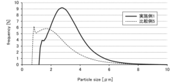
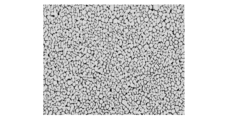
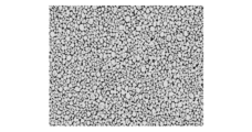
図1は、本発明の実施例1及び比較例5で用いた粉末の個数基準の粒度分布を示す図である。図1では、実施例1で用いた粉末の粒度分布は粒子径が小さい領域(2μm以下)にピークが殆どなく、粒子径が小さい粒子が少ないことが分かる。これに対し、比較例5で用いた粉末の粒度分布は0.81μmの箇所に大きなピークがあり、粒子径が小さい粒子が多いことが分かる。 Figure 1 shows the particle size distribution based on the number of particles used in Example 1 and Comparative Example 5 of the present invention. In Figure 1, the particle size distribution of the powder used in Example 1 has almost no peak in the small particle size region (2 μm or less), and it can be seen that there are few particles with small particle sizes. In contrast, the particle size distribution of the powder used in Comparative Example 5 has a large peak at 0.81 μm, and it can be seen that there are many particles with small particle sizes.
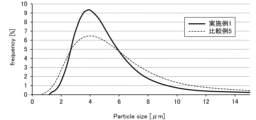
図2は、本発明の実施例1及び比較例5で用いた粉末の体積基準の粒度分布を示す図である。図2では、実施例1及び比較例5で用いた粉末は、両方とも粒子径が小さい領域(2μm以下)にピークが見られず、体積基準の粒度分布では粒子径が小さい粒子の存在は不明である。 Figure 2 shows the volumetric particle size distribution of the powders used in Example 1 of the present invention and Comparative Example 5. In Figure 2, the powders used in Example 1 and Comparative Example 5 do not show a peak in the small particle size region (2 μm or less), and the presence of small particles is unclear in the volumetric particle size distribution.
以下、本発明の電極材について詳細に説明する。 The electrode material of the present invention is described in detail below.
(焼結体)
本発明の電極材は、アルミニウム箔基材の少なくとも片面に、アルミニウム粉末及びアルミニウム合金粉末からなる群より選択される少なくとも1種の粉末の焼結体を有する。
(Sintered body)
The electrode material of the present invention has, on at least one surface of an aluminum foil substrate, a sintered body of at least one type of powder selected from the group consisting of aluminum powder and aluminum alloy powder.
焼結体は、アルミニウム箔基材の少なくとも片面に形成されていればよく、両面に形成されていてもよい。電極材の静電容量がより一層向上する点で、両面に形成されていることが好ましい。 The sintered body needs to be formed on at least one side of the aluminum foil substrate, and may be formed on both sides. It is preferable that the sintered body be formed on both sides, as this further improves the capacitance of the electrode material.
焼結体は、上記粉末同士が空隙を維持しながら焼結して接合されることにより、三次元網目構造を有する多孔質焼結体であることが好ましい。当該構造を有することにより、焼結体の表面積が大きくなり、高い静電容量を示すアルミニウム電解コンデンサ(以下、単に「コンデンサ」とも示す。)を製造可能な電極材を得ることができる。 The sintered body is preferably a porous sintered body having a three-dimensional mesh structure, which is formed by sintering and bonding the powders together while maintaining voids. By having this structure, the surface area of the sintered body is increased, and it is possible to obtain an electrode material that can be used to manufacture aluminum electrolytic capacitors (hereinafter also simply referred to as "capacitors") that exhibit high electrostatic capacitance.
アルミニウム粉末のアルミニウム含有量は、99.80質量%以上であることが好ましく、99.85質量%以上であることがより好ましく、99.99質量%以上であることが更に好ましい。 The aluminum content of the aluminum powder is preferably 99.80% by mass or more, more preferably 99.85% by mass or more, and even more preferably 99.99% by mass or more.
アルミニウム合金粉末は、珪素(Si)、鉄(Fe)、銅(Cu)、マンガン(Mn)、マグネシウム(Mg)、クロム(Cr)、亜鉛(Zn)、チタン(Ti)、バナジウム(V)、ガリウム(Ga)、ニッケル(Ni)、ホウ素(B)、ジルコニウム(Zr)等から選ばれる1種以上の元素を含んでもよい。アルミニウム合金中のこれらの元素の含有量は、100質量ppm以下が好ましく、50質量ppm以下がより好ましい。アルミニウム合金粉末中の上記元素の含有量が上記範囲であることにより、アルミニウム電解コンデンサ用電極材の静電容量がより一層向上する。 The aluminum alloy powder may contain one or more elements selected from silicon (Si), iron (Fe), copper (Cu), manganese (Mn), magnesium (Mg), chromium (Cr), zinc (Zn), titanium (Ti), vanadium (V), gallium (Ga), nickel (Ni), boron (B), zirconium (Zr), etc. The content of these elements in the aluminum alloy is preferably 100 ppm by mass or less, and more preferably 50 ppm by mass or less. When the content of the above elements in the aluminum alloy powder is within the above range, the capacitance of the electrode material for aluminum electrolytic capacitors is further improved.
上記粉末は、一種単独で用いてもよいし、二種以上を混合して用いてもよい。 The above powders may be used alone or in combination of two or more.
焼結体中の粉末の個数基準の粒度分布における50%粒子径D50(以下、「個数基準の粒子径D50」、「D50」とも示す。)は、2.0μm以上3.5μm以下である。個数基準の粒子径D50が2.0μm未満であるか、又は、3.5μmを超えると、電極材の静電容量が十分でない。上記焼結体中の粉末の個数基準の粒子径D50は2.2μm以上3.3μm以下が好ましく、2.3μm以上3.0μm以下がより好ましく、2.4μm以上2.8μm以下がより好ましい。 The 50% particle diameter D50 in the number-based particle size distribution of the powder in the sintered body (hereinafter also referred to as "number-based particle diameter D50 " or " D50 ") is 2.0 μm or more and 3.5 μm or less. If the number-based particle diameter D50 is less than 2.0 μm or more or exceeds 3.5 μm, the capacitance of the electrode material is insufficient. The number-based particle diameter D50 of the powder in the sintered body is preferably 2.2 μm or more and 3.3 μm or less, more preferably 2.3 μm or more and 3.0 μm or less, and more preferably 2.4 μm or more and 2.8 μm or less.
本明細書において、焼結体中の粉末の個数基準の粒子径D50は、焼結体の断面を、走査型電子顕微鏡で観察することによって測定することができる。具体的には、上記粉末を焼結して焼結体を形成すると、当該焼結体では粒子状の粉末の一部が焼結して、粉末同士が接合した状態となる。焼結体の断面において、接合した状態の各粉末の最大径(長径)をその粉末の粒子径とし、断面画像中の一定面積中の全粒子の粒子径と粒子数を求める。求めた全粒子を粒子径が小さい順にならべ、粒子数の50%となる順番目の粒子径を焼結体中の粉末の個数基準の粒子径D50とする。また粒子数の10%、90%となる順番目の粒子径をそれぞれ下記の、焼結体中の粉末の個数基準の粒子径D10、D90とする。 In this specification, the particle diameter D50 based on the number of powders in the sintered body can be measured by observing the cross section of the sintered body with a scanning electron microscope. Specifically, when the above powders are sintered to form a sintered body, a part of the particulate powder is sintered in the sintered body, and the powders are bonded together. In the cross section of the sintered body, the maximum diameter (long diameter) of each powder in the bonded state is taken as the particle diameter of the powder, and the particle diameter and number of all particles in a certain area in the cross section image are obtained. The obtained all particles are arranged in order of smallest particle diameter, and the particle diameter that is 50% of the number of particles is taken as the particle diameter D50 based on the number of powders in the sintered body. The particle diameters that are 10% and 90% of the number of particles are taken as the particle diameters D10 and D90 based on the number of powders in the sintered body, respectively, as follows.
焼結体中の粉末の個数基準の粒子径D10は、1.0μm以上1.8μm以下である。個数基準の粒子径D10が1.0μm未満であると、焼結体中の粉末中の微細な粉末が多くなり、クラックの原因となるような二次粒子の数が増大し電極材の折り曲げ強度が低下する。個数基準の粒子径D10が1.8μmを超えると、材料のアルミニウム粉末の製造工程での収率が低下しコストが増大する。上記焼結体中の粉末の個数基準の粒子径D10は折曲強度やコストの点で1.3μm以上1.7μm以下が好ましく、1.4μm以上1.5μm以下がより好ましい。 The number-based particle diameter D10 of the powder in the sintered body is 1.0 μm or more and 1.8 μm or less. If the number-based particle diameter D10 is less than 1.0 μm, the amount of fine powder in the powder in the sintered body increases, the number of secondary particles that cause cracks increases, and the bending strength of the electrode material decreases. If the number-based particle diameter D10 exceeds 1.8 μm, the yield in the manufacturing process of the aluminum powder material decreases and the cost increases. The number-based particle diameter D10 of the powder in the sintered body is preferably 1.3 μm or more and 1.7 μm or less, and more preferably 1.4 μm or more and 1.5 μm or less, in terms of bending strength and cost.
焼結体中の粉末の個数基準の粒子径D90は、3.8μm以上6.0μm以下である。個数基準の粒子径D90が3.8μm未満であると、材料のアルミニウム粉末の製造工程での収率が低下しコストが増大する。個数基準の粒子径D90が6.0μmを超えると焼結体の表面積が十分でなく、コンデンサ用電極材とした際に静電容量が十分でない。上記焼結体中の粉末の個数基準の粒子径D90はコンデンサ用電極材とした際の静電容量の点で3.9μm以上5.0μm以下が好ましく、3.9μm以上4.5μm以下がより好ましい。 The number-based particle diameter D 90 of the powder in the sintered body is 3.8 μm or more and 6.0 μm or less. If the number-based particle diameter D 90 is less than 3.8 μm, the yield in the manufacturing process of the aluminum powder material decreases and the cost increases. If the number-based particle diameter D 90 exceeds 6.0 μm, the surface area of the sintered body is insufficient, and the capacitance is insufficient when used as an electrode material for a capacitor. The number-based particle diameter D 90 of the powder in the sintered body is preferably 3.9 μm or more and 5.0 μm or less, more preferably 3.9 μm or more and 4.5 μm or less, in terms of the capacitance when used as an electrode material for a capacitor.
なお、上述の測定方法により測定される焼結体中の粉末の個数基準の粒子径D10、D50、D90は、焼結前の粉末の個数基準の粒子径D10、D50、D90から殆ど変化せず、略同一であるので、焼結前の粉末の個数基準の粒子径D10、D50、D90の測定値を、焼結体中の粉末の個数基準の粒子径D10、D50、D90とすることができる。本明細書において、上記焼結前の粉末の個数基準の粒子径D10、D50、D90は、マイクロトラックMT3300EXII(日機装株式会社製)を使用し、レーザー回折・散乱法湿式測定により粒度分布を個数基準で測定し、D10値、D50値及びおよびD90値を算出することにより測定することができる。 In addition, the number-based particle diameters D10 , D50 , and D90 of the powder in the sintered body measured by the above-mentioned measuring method are almost the same as the number-based particle diameters D10 , D50 , and D90 of the powder before sintering, and therefore the measured values of the number-based particle diameters D10 , D50 , and D90 of the powder before sintering can be used as the number-based particle diameters D10 , D50 , and D90 of the powder in the sintered body. In this specification, the number-based particle diameters D10 , D50 , and D90 of the powder before sintering can be measured by measuring the particle size distribution on a number basis by laser diffraction/scattering wet measurement using a Microtrac MT3300EXII (manufactured by Nikkiso Co., Ltd.) and calculating the D10 value, D50 value, and D90 value.
上記個数基準の粒度分布におけるD10、D50、D90が上記範囲である粉末は、アトマイズしたアルミニウム粉末を、渦式分級や篩分級等の方法により分級することで得ることができる。具体的には、(1)D10が上記範囲となる分級機、D50が上記範囲となる分級機、及び、D90が上記範囲となる分級機を組み合わせて使用し、アトマイズしたアルミニウム粉末を分級する方法、(2)アトマイズしたアルミニウム粉末を渦式分級、篩分級等の方法により分級して、D10が上記範囲であるアルミニウム粉末、D50が上記範囲であるアルミニウム粉末、D90が上記範囲であるアルミニウム粉末をそれぞれ調製し、これらを混合する方法等により得ることができる。 The powder having D10 , D50 , and D90 in the number-based particle size distribution in the above ranges can be obtained by classifying atomized aluminum powder by methods such as vortex classification, sieve classification, etc. Specifically, the powder can be obtained by (1) a method of classifying atomized aluminum powder using a combination of a classifier having D10 in the above range, a classifier having D50 in the above range, and a classifier having D90 in the above range, or (2) a method of classifying atomized aluminum powder by methods such as vortex classification, sieve classification, etc. to prepare aluminum powder having D10 in the above range, aluminum powder having D50 in the above range , and aluminum powder having D90 in the above range, respectively, and mixing these.
焼結体の合計厚みは50μm以上900μmである。焼結体の合計厚みが50μm未満であると、電極材の静電容量が十分でない。合計厚みが900μmを超える焼結体は、形成が困難である。焼結体の合計厚みは、70μm以上が好ましく、100μm以上がより好ましい。また、焼結体の合計厚みは、875μm以下が好ましく、860μm以下がより好ましく、500μm以下が更に好ましく、300μm以下が特に好ましい。なお、本明細書において焼結体の合計厚みとは、本発明の電極材が焼結体をアルミニウム箔基材の両面に有する場合は、それぞれの面に形成された焼結体の厚みの合計の厚みである。本発明の電極材が焼結体をアルミニウム箔基材の片面のみに有する場合は、片面の焼結体の厚みが合計厚みとなる。 The total thickness of the sintered body is 50 μm or more and 900 μm. If the total thickness of the sintered body is less than 50 μm, the capacitance of the electrode material is insufficient. If the total thickness of the sintered body exceeds 900 μm, it is difficult to form the sintered body. The total thickness of the sintered body is preferably 70 μm or more, more preferably 100 μm or more. The total thickness of the sintered body is preferably 875 μm or less, more preferably 860 μm or less, even more preferably 500 μm or less, and particularly preferably 300 μm or less. In this specification, the total thickness of the sintered body is the total thickness of the thicknesses of the sintered bodies formed on each side when the electrode material of the present invention has a sintered body on both sides of the aluminum foil base material. When the electrode material of the present invention has a sintered body on only one side of the aluminum foil base material, the thickness of the sintered body on one side is the total thickness.
焼結体の表面の100μm×115μmの任意の領域内の粒子径1μm以下の粉末の数は、300個以下が好ましく、250個以下がより好ましく、200個以下が更に好ましく、180個以下が特に好ましい。上記粒子径1μm以下の粉末の数の上限が上記範囲であることにより、焼結体中の粉末中の微細な粉末が少なくなり、クラックの原因となるような二次粒子の数の増大が抑制されて、本発明の電極材の折曲強度がより一層向上するため、電極材をコンデンサ用電極とする際の、陽極酸化処理ライン中や捲回工程での破断をより一層抑制することができる。また、上記粒子径1μm以下の粉末の数の下限は少ない程好ましいが、0個、50個以上、100個以上であってもよい。 The number of powder particles having a particle diameter of 1 μm or less in any region of 100 μm x 115 μm on the surface of the sintered body is preferably 300 or less, more preferably 250 or less, even more preferably 200 or less, and particularly preferably 180 or less. By setting the upper limit of the number of powder particles having a particle diameter of 1 μm or less within the above range, the amount of fine powder in the powder in the sintered body is reduced, and an increase in the number of secondary particles that cause cracks is suppressed, and the bending strength of the electrode material of the present invention is further improved, so that breakage during the anodizing process or winding process when the electrode material is used as a capacitor electrode can be further suppressed. In addition, the lower limit of the number of powder particles having a particle diameter of 1 μm or less is preferably as low as possible, but it may be 0, 50 or more, or 100 or more.
本明細書において、焼結体の表面の100μm×115μmの任意の領域内の粒子径1μm以下の粉末の数は、焼結体表面を、走査型電子顕微鏡で撮影した画像を画像解析ソフトで画像処理した後、解析し、焼結体の表面の100μm×115μmの任意の領域内の粒子径1μm以下の粉末の数を数えることにより測定することができる。以下、より具体的に説明する。 In this specification, the number of powder particles with a particle diameter of 1 μm or less within any given 100 μm x 115 μm area on the surface of the sintered body can be measured by analyzing an image of the sintered body surface taken with a scanning electron microscope, processing the image with image analysis software, and counting the number of powder particles with a particle diameter of 1 μm or less within any given 100 μm x 115 μm area on the surface of the sintered body. This will be explained in more detail below.
走査型電子顕微鏡での撮影は、JEOL社製の走査電子顕微鏡(品番:JSM-5510)をい用いて、二次電子像、撮影倍率1500倍、加速電圧15kV、スポット径15、作動距離20mmの条件で行う。 Scanning electron microscope photography was performed using a JEOL scanning electron microscope (product number: JSM-5510) under the following conditions: secondary electron image, magnification of 1500x, acceleration voltage of 15 kV, spot diameter of 15, and working distance of 20 mm.
次いで、三谷商事株式会社製の画像解析ソフトWinROOF2015により焼結体層表面の粒子径1μm以下の粉末の個数を算出する。具体的には、走査電子顕微鏡で撮影した画像をJPEGイメージでソフトに取り込み、「モノクロ化」処理を行い、次いで「二値化」処理を行う。その後、画像内の任意の100μm×115μmの範囲内で、各粉末の円相当径をその粉末の粒子径とし、粒子径1μm以下の粉末の個数を数えることにより測定する。 Next, the number of powder particles with a particle diameter of 1 μm or less on the surface of the sintered layer is calculated using image analysis software WinROOF2015 made by Mitani Shoji Co., Ltd. Specifically, the image taken with the scanning electron microscope is imported into the software as a JPEG image, and a "monochrome conversion" process is performed, followed by a "binarization" process. After that, within any 100 μm x 115 μm range in the image, the circle equivalent diameter of each powder particle is taken as the particle diameter of that powder, and the number of powder particles with a particle diameter of 1 μm or less is counted to measure.
(アルミニウム箔基材、アルミニウム合金箔基材)
本発明の電極材は、アルミニウム箔基材又はアルミニウム合金箔基材(以下、併せて「基材」とも示す。)を有する。
(Aluminum foil substrate, aluminum alloy foil substrate)
The electrode material of the present invention has an aluminum foil substrate or an aluminum alloy foil substrate (hereinafter, also referred to as "substrate").
アルミニウム箔基材を形成するアルミニウム箔としては、純アルミニウムからなるアルミニウム箔を使用することが好ましい。 It is preferable to use an aluminum foil made of pure aluminum as the aluminum foil that forms the aluminum foil substrate.
純アルミニウムからなるアルミニウム箔のアルミニウム含有量は、99.80質量%以上であることが好ましく、99.85質量%以上であることがより好ましく、99.99質量%以上であることが更に好ましい。 The aluminum content of the aluminum foil made of pure aluminum is preferably 99.80% by mass or more, more preferably 99.85% by mass or more, and even more preferably 99.99% by mass or more.
アルミニウム合金箔基材を形成するアルミニウム合金箔に用いられるアルミニウム合金は、珪素(Si)、鉄(Fe)、銅(Cu)、マンガン(Mn)、マグネシウム(Mg)、クロム(Cr)、亜鉛(Zn)、チタン(Ti)、バナジウム(V)、ガリウム(Ga)、ニッケル(Ni)及びホウ素(B)からなる群より選択される少なくとも1種の金属元素を必要範囲内において、アルミニウムに添加したアルミニウム合金であってもよいし、上記元素を不可避的不純物的に含むアルミニウム合金であってもよい。アルミニウム合金中のこれらの元素の含有量は、100質量ppm以下が好ましく、50質量ppm以下がより好ましい。アルミニウム合金中の上記元素の含有量が上記範囲であることにより、アルミニウム電解コンデンサ用電極材の静電容量がより一層向上する。 The aluminum alloy used in the aluminum alloy foil forming the aluminum alloy foil substrate may be an aluminum alloy in which at least one metal element selected from the group consisting of silicon (Si), iron (Fe), copper (Cu), manganese (Mn), magnesium (Mg), chromium (Cr), zinc (Zn), titanium (Ti), vanadium (V), gallium (Ga), nickel (Ni) and boron (B) is added to aluminum within the required range, or may be an aluminum alloy containing the above elements as unavoidable impurities. The content of these elements in the aluminum alloy is preferably 100 ppm by mass or less, more preferably 50 ppm by mass or less. By having the content of the above elements in the aluminum alloy within the above range, the capacitance of the electrode material for aluminum electrolytic capacitors is further improved.
基材の厚みは、電極材の強度がより一層向上する観点から、10μm以上が好ましく、15μm以上がより好ましく、20μm以上が更に好ましい。また、アルミニウム箔基材の厚みは、コンデンサ用電極材とした際の体積あたりの容量がより一層向上する観点から、80μm以下が好ましく、60μm以下がより好ましく、40μm以下が更に好ましい。 The thickness of the substrate is preferably 10 μm or more, more preferably 15 μm or more, and even more preferably 20 μm or more, from the viewpoint of further improving the strength of the electrode material. The thickness of the aluminum foil substrate is preferably 80 μm or less, more preferably 60 μm or less, and even more preferably 40 μm or less, from the viewpoint of further improving the capacity per volume when used as an electrode material for a capacitor.
(陽極酸化皮膜)
本発明の電極材は、上記焼結体の表面に、更に、陽極酸化皮膜を有していてもよい。焼結体の表面に陽極酸化皮膜を有することにより、当該陽極酸化皮膜が誘電体として機能することで、本発明の電極材をアルミニウム電解コンデンサ用電極材として有用に用いることができる。
(anodic oxide film)
The electrode material of the present invention may further have an anodized film on the surface of the sintered body. By having an anodized film on the surface of the sintered body, the anodized film functions as a dielectric, and the electrode material of the present invention can be usefully used as an electrode material for an aluminum electrolytic capacitor.
陽極酸化皮膜は、焼結体の表面を陽極酸化することにより作製することができる。上記陽極酸化皮膜は、誘電体皮膜としての機能を有する。 The anodized film can be produced by anodizing the surface of the sintered body. The anodized film functions as a dielectric film.
陽極酸化皮膜の厚みは0.2~1.1μmが好ましく、0.3~1.05μmがより好ましい。 The thickness of the anodized film is preferably 0.2 to 1.1 μm, and more preferably 0.3 to 1.05 μm.
陽極酸化皮膜の皮膜耐電圧は250~800Vが好ましく、300~800Vがより好ましい。陽極酸化皮膜の皮膜耐電圧は、日本電子機械工業会規格RC-2364Aに準拠した測定方法により測定することができる。 The film withstand voltage of the anodized film is preferably 250 to 800 V, and more preferably 300 to 800 V. The film withstand voltage of the anodized film can be measured using a method that complies with the Japan Electronics Industries Association standard RC-2364A.
2.アルミニウム電解コンデンサ用電極材の製造方法
本発明のアルミニウム電解コンデンサ用電極材の製造方法は、
(1)アルミニウム箔基材又はアルミニウム合金箔基材の少なくとも片面に、アルミニウム粉末及びアルミニウム合金粉末からなる群より選択される少なくとも1種の粉末を含むペースト組成物の皮膜を形成する第1工程、及び
(2)前記皮膜を560℃以上660℃以下の温度で焼結する第2工程を含み、
前記粉末は、個数基準の粒度分布における10%粒子径D10が1.0~1.8μmであり、個数基準の粒度分布における50%粒子径D50が2.0~3.5μmであり、個数基準の粒度分布における90%粒子径D90が3.8~6.0μmである製造方法である。以下、詳細に説明する。
2. Method for producing an electrode material for an aluminum electrolytic capacitor The method for producing an electrode material for an aluminum electrolytic capacitor of the present invention includes the steps of:
(1) a first step of forming a coating of a paste composition containing at least one powder selected from the group consisting of aluminum powder and aluminum alloy powder on at least one surface of an aluminum foil substrate or an aluminum alloy foil substrate; and (2) a second step of sintering the coating at a temperature of 560° C. or higher and 660° C. or lower.
The powder is produced by a method such that the 10% particle diameter D10 in the particle size distribution based on the number of particles is 1.0 to 1.8 μm, the 50% particle diameter D50 in the particle size distribution based on the number of particles is 2.0 to 3.5 μm, and the 90% particle diameter D90 in the particle size distribution based on the number of particles is 3.8 to 6.0 μm. This will be described in detail below.
(第1工程)
第1工程は、(1)アルミニウム箔基材又はアルミニウム合金箔基材(以下、併せて「基材」とも示す。)の少なくとも片面に、アルミニウム粉末及びアルミニウム合金粉末からなる群より選択される少なくとも1種の粉末を含むペースト組成物の皮膜を形成する工程である。
(First step)
The first step is (1) forming a coating of a paste composition containing at least one type of powder selected from the group consisting of aluminum powder and aluminum alloy powder on at least one surface of an aluminum foil substrate or an aluminum alloy foil substrate (hereinafter, also referred to as "substrate").
原料のアルミニウムの粉末としては、例えば、アルミニウム純度99.80質量%以上のアルミニウム粉末が好ましく、アルミニウム純度99.85質量%以上のアルミニウム粉末がより好ましく、アルミニウム純度99.99質量%以上のアルミニウム粉末が更に好ましい。また、原料のアルミニウム合金粉末としては、例えば、珪素(Si)、鉄(Fe)、銅(Cu)、マンガン(Mn)、マグネシウム(Mg)、クロム(Cr)、亜鉛(Zn)、チタン(Ti)、バナジウム(V)、ガリウム(Ga)、ニッケル(Ni)、ホウ素(B)、ジルコニウム(Zr)等の元素のうち、1種又は2種以上を含む合金が好ましい。アルミニウム合金中のこれらの元素の含有量は、100質量ppm以下、特に50質量ppm以下とすることが好ましい。 As the raw aluminum powder, for example, aluminum powder with an aluminum purity of 99.80 mass% or more is preferable, aluminum powder with an aluminum purity of 99.85 mass% or more is more preferable, and aluminum powder with an aluminum purity of 99.99 mass% or more is even more preferable. In addition, as the raw aluminum alloy powder, for example, an alloy containing one or more of elements such as silicon (Si), iron (Fe), copper (Cu), manganese (Mn), magnesium (Mg), chromium (Cr), zinc (Zn), titanium (Ti), vanadium (V), gallium (Ga), nickel (Ni), boron (B), zirconium (Zr), etc. is preferable. The content of these elements in the aluminum alloy is preferably 100 mass ppm or less, particularly 50 mass ppm or less.
上記粉末は、一種単独で用いてもよいし、二種以上を混合して用いてもよい。 The above powders may be used alone or in combination of two or more.
粉末の個数基準の粒度分布における50%粒子径D50は、2.0μm以上3.5μm以下である。個数基準の粒子径D50が2.0μm未満であるか、又は、3.5μmを超えると、製造される電極材の静電容量が十分でない。上記粉末の個数基準の粒子径D50は2.2μm以上3.3μm以下が好ましく、2.3μm以上3.0μm以下がより好ましく、2.4μm以上2.8μm以下がより好ましい。 The 50% particle diameter D50 in the particle size distribution based on the number of the powder is 2.0 μm or more and 3.5 μm or less. If the particle diameter D50 based on the number of the powder is less than 2.0 μm or more and exceeds 3.5 μm, the capacitance of the electrode material produced is insufficient. The particle diameter D50 based on the number of the powder is preferably 2.2 μm or more and 3.3 μm or less, more preferably 2.3 μm or more and 3.0 μm or less, and more preferably 2.4 μm or more and 2.8 μm or less.
粉末の個数基準の粒子径D10は、1.0μm以上1.8μm以下である。個数基準の粒子径D10が1.0μm未満であると、粉末中の微細な粉末が多くなり、クラックの原因となるような二次粒子の数が増大し、製造される電極材の折り曲げ強度が低下する。個数基準の粒子径D10が1.8μmを超えると、材料のアルミニウム粉末の製造工程での収率が低下しコストが増大する。上記粉末の個数基準の粒子径D10は折曲強度やコストの点で1.3μm以上1.7μm以下が好ましく、1.4μm以上1.5μm以下がより好ましい。 The number-based particle diameter D 10 of the powder is 1.0 μm or more and 1.8 μm or less. If the number-based particle diameter D 10 is less than 1.0 μm, the amount of fine powder in the powder increases, the number of secondary particles that cause cracks increases, and the bending strength of the electrode material produced decreases. If the number-based particle diameter D 10 exceeds 1.8 μm, the yield in the manufacturing process of the aluminum powder material decreases and the cost increases. The number-based particle diameter D 10 of the powder is preferably 1.3 μm or more and 1.7 μm or less, more preferably 1.4 μm or more and 1.5 μm or less, in terms of bending strength and cost.
粉末の個数基準の粒子径D90は、3.8μm以上6.0μm以下である。個数基準の粒子径D90が3.8μm未満であると、材料のアルミニウム粉末の製造工程での収率が低下しコストが増大する。個数基準の粒子径D90が6.0μmを超えると焼結体の表面積が十分でなく、コンデンサ用電極材とした際に静電容量が十分でない。上記粉末の個数基準の粒子径D90はコンデンサ用電極材とした際の静電容量の点で3.9μm以上5.0μm以下が好ましく、3.9μm以上4.5μm以下がより好ましい。 The number-based particle diameter D 90 of the powder is 3.8 μm or more and 6.0 μm or less. If the number-based particle diameter D 90 is less than 3.8 μm, the yield in the manufacturing process of the aluminum powder material decreases and the cost increases. If the number-based particle diameter D 90 exceeds 6.0 μm, the surface area of the sintered body is insufficient, and the capacitance is insufficient when used as an electrode material for a capacitor. The number-based particle diameter D 90 of the powder is preferably 3.9 μm or more and 5.0 μm or less, more preferably 3.9 μm or more and 4.5 μm or less, in terms of the capacitance when used as an electrode material for a capacitor.
なお、粉末の個数基準の粒子径D10、D50、D90は、マイクロトラックMT3300EXII(日機装株式会社製)を使用し、レーザー回折・散乱法湿式測定により粒度分布を個数基準で測定し、D10値、D50値及びおよびD90値を算出することにより測定することができる。 The number-based particle diameters D10 , D50 , and D90 of the powder can be measured by measuring the particle size distribution on a number basis by wet measurement using a Microtrac MT3300EXII (manufactured by Nikkiso Co., Ltd.) using a laser diffraction/scattering method, and calculating the D10 value, D50 value, and D90 value.
上記個数基準の粒度分布におけるD10、D50、D90が上記範囲である粉末は、アトマイズしたアルミニウム粉末を、渦式分級や篩分級等の方法により分級することで得ることができる。具体的には、(1)D10が上記範囲となる分級機、D50が上記範囲となる分級機、及び、D90が上記範囲となる分級機を組み合わせて使用し、アトマイズしたアルミニウム粉末を分級する方法、(2)アトマイズしたアルミニウム粉末を渦式分級、篩分級等の方法により分級して、D10が上記範囲であるアルミニウム粉末、D50が上記範囲であるアルミニウム粉末、D90が上記範囲であるアルミニウム粉末をそれぞれ調製し、これらを混合する方法等により得ることができる。 The powder having D10 , D50 , and D90 in the number-based particle size distribution in the above ranges can be obtained by classifying atomized aluminum powder by methods such as vortex classification, sieve classification, etc. Specifically, the powder can be obtained by (1) a method of classifying atomized aluminum powder using a combination of a classifier having D10 in the above range, a classifier having D50 in the above range, and a classifier having D90 in the above range, or (2) a method of classifying atomized aluminum powder by methods such as vortex classification, sieve classification, etc. to prepare aluminum powder having D10 in the above range, aluminum powder having D50 in the above range , and aluminum powder having D90 in the above range, respectively, and mixing these.
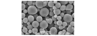
アルミニウム粉末及びアルミニウム合金粉末の形状は、特に限定されず、球状、不定形状、鱗片状、繊維状等のいずれも好適に使用できるが、工業的生産には球状粒子からなる粉末が特に好ましい。 The shape of the aluminum powder and aluminum alloy powder is not particularly limited, and any shape such as spherical, irregular, scaly, or fibrous can be suitably used, but for industrial production, powders consisting of spherical particles are particularly preferred.
ペースト組成物は、樹脂バインダーを含有していてもよい。樹脂バインダーについては、公知のものを広く採用することができ、例えば、カルボキシ変性ポリオレフィン樹脂、酢酸ビニル樹脂、塩化ビニル樹脂、塩酢ビ共重合樹脂、ビニルアルコール樹脂、ブチラール樹脂、フッ化ビニル樹脂、アクリル樹脂、ポリエステル樹脂、ウレタン樹脂、エポキシ樹脂、尿素樹脂、フェノール樹脂、アクリロニトリル樹脂、セルロース樹脂、パラフィンワックス、ポリエチレンワックス等の合成樹脂、並びに、ワックス、タール、にかわ、ウルシ、松脂、ミツロウ等の天然樹脂又はワックスが好適に使用できる。これらの樹脂バインダーは、分子量、樹脂の種類等により、加熱時に揮発するものと、熱分解によりその残渣がアルミニウム粉末とともに残存するものとがあり、所望の静電容量等の電気特性に応じて使い分けることができる。 The paste composition may contain a resin binder. A wide variety of known resin binders can be used, including, for example, synthetic resins such as carboxy-modified polyolefin resins, vinyl acetate resins, vinyl chloride resins, vinyl chloride-vinyl acetate copolymer resins, vinyl alcohol resins, butyral resins, vinyl fluoride resins, acrylic resins, polyester resins, urethane resins, epoxy resins, urea resins, phenolic resins, acrylonitrile resins, cellulose resins, paraffin wax, and polyethylene wax, as well as natural resins or waxes such as wax, tar, glue, urushi, rosin, and beeswax. Depending on the molecular weight, type of resin, and the like, some of these resin binders volatilize when heated, while others remain as residues together with the aluminum powder after thermal decomposition. These resin binders can be used according to the desired electrical properties, such as capacitance.
ペースト組成物中の樹脂バインダーの含有量は、ペースト状組成物100質量%中に0.5~10質量%とすることが好ましく、0.75~5質量%とすることがより好ましい。ペースト組成物中の樹脂バインダー量が0.5質量%以上であることにより、基材と未焼結積層体との密着強度を向上できる。一方、樹脂バインダー量が10質量%以下であることにより、焼結工程及び脱脂工程において脱脂しやすく、樹脂バインダーが残留する事によって発生する不具合を抑制できる。 The content of the resin binder in the paste composition is preferably 0.5 to 10 mass% and more preferably 0.75 to 5 mass% in 100 mass% of the paste-like composition. By having the amount of resin binder in the paste composition be 0.5 mass% or more, the adhesive strength between the substrate and the unsintered laminate can be improved. On the other hand, by having the amount of resin binder be 10 mass% or less, degreasing is easy in the sintering process and the degreasing process, and defects caused by residual resin binder can be suppressed.
その他、必要に応じて適宜、ペースト組成物中には溶剤、焼結助剤、界面活性剤等が含まれていてもよい。これらはいずれも公知又は市販のものを使用することができる。これにより効率よく皮膜を形成することができる。 In addition, the paste composition may contain a solvent, a sintering aid, a surfactant, etc., as necessary. All of these can be publicly known or commercially available. This allows the film to be formed efficiently.
溶剤としては、公知の溶剤を広く採用することがきる。例えば、水;トルエン、アルコール類、ケトン類、エステル類等の有機溶剤を使用することができる。 A wide variety of known solvents can be used as the solvent. For example, water, toluene, alcohols, ketones, esters, and other organic solvents can be used.
焼結助剤としても、公知の焼結助剤を広く使用することができる。例えば、アルミニウムフッ化物、カリウムフッ化物等を使用することができる。 As a sintering aid, a wide variety of known sintering aids can be used. For example, aluminum fluoride, potassium fluoride, etc. can be used.
界面活性剤としても、公知の界面活性剤を広く使用することができる。例えば、ベタイン系、スルホベタイン系、アルキルベタイン系等の界面活性剤を使用することができる。 As the surfactant, a wide variety of known surfactants can be used. For example, betaine, sulfobetaine, alkylbetaine, and other surfactants can be used.
上記のペースト組成物を、基材の片面又は両面に付着させてペースト組成物の皮膜を形成するに際し、皮膜の合計の厚みは、50μm以上900μm以下とすることが好ましい。また、皮膜の合計の厚みは、70μm以上が好ましく、100μm以上がより好ましい。また、皮膜の合計厚みは、875μm以下が好ましく、860μm以下がより好ましく、500μm以下が更に好ましく、300μm以下が特に好ましい。なお、本明細書において皮膜の合計厚みとは、第1工程において皮膜を基材の両面に形成する場合は、それぞれの面に形成された皮膜の厚みの合計の厚みである。第1工程において皮膜を基材の片面のみに形成する場合は、片面の皮膜の厚みが合計厚みとなる。 When the paste composition is applied to one or both sides of a substrate to form a film of the paste composition, the total thickness of the film is preferably 50 μm or more and 900 μm or less. The total thickness of the film is preferably 70 μm or more, and more preferably 100 μm or more. The total thickness of the film is preferably 875 μm or less, more preferably 860 μm or less, even more preferably 500 μm or less, and particularly preferably 300 μm or less. In this specification, the total thickness of the film is the total thickness of the film formed on each side when the film is formed on both sides of the substrate in the first step. When the film is formed on only one side of the substrate in the first step, the thickness of the film on one side is the total thickness.
基材上に皮膜を形成する形成方法としては特に限定されず、ペースト組成物を、例えばダイコート、グラビアコート、ダイレクトコート、ローラー、刷毛、スプレー、ディッピング等の塗布方法を用いて形成できるほか、シルクスクリーン印刷等の公知の印刷方法により形成することもできる。 The method for forming a film on a substrate is not particularly limited, and the paste composition can be applied by a coating method such as die coating, gravure coating, direct coating, roller coating, brush coating, spraying, dipping, or by a known printing method such as silk screen printing.
また、必要に応じて基材上に付着させた皮膜を、基材と共に20~300℃の範囲内の温度で1~30分間乾燥させることも好ましい。 If necessary, it is also preferable to dry the coating applied to the substrate together with the substrate at a temperature in the range of 20 to 300°C for 1 to 30 minutes.
(第2工程)
第2工程は、(2)前記皮膜を560℃以上660℃以下の温度で焼結する工程である。
(Second step)
The second step is (2) sintering the coating at a temperature of 560°C or higher and 660°C or lower.
第2工程により皮膜中の粉末が焼結され、基材上に焼結体が形成される。焼結温度は560℃以上660℃以下である。焼結温度が560℃未満であると、焼結が進まず所望の静電容量が得られない。焼結温度が660℃を超えると、粉末が溶融して、電解コンデンサの電極材として使用した場合に十分な容量が得られない。焼結温度は、570℃以上650℃未満が好ましく、580℃以上620℃未満がより好ましい。 In the second step, the powder in the coating is sintered to form a sintered body on the substrate. The sintering temperature is 560°C or higher and 660°C or lower. If the sintering temperature is lower than 560°C, sintering does not proceed and the desired capacitance is not obtained. If the sintering temperature exceeds 660°C, the powder melts and sufficient capacitance is not obtained when used as an electrode material for an electrolytic capacitor. The sintering temperature is preferably 570°C or higher and lower than 650°C, and more preferably 580°C or higher and lower than 620°C.
焼結時間は焼結温度等にも影響されるが、通常は5~24時間程度の範囲内で適宜決定することができる。焼結雰囲気は、特に制限されず、例えば真空雰囲気、不活性ガス雰囲気、酸化性ガス雰囲気(大気)、還元性雰囲気等のいずれであってもよいが、特に真空雰囲気又は還元性雰囲気とすることが好ましい。また、圧力条件についても、常圧、減圧又は加圧のいずれであってもよい。 The sintering time is affected by the sintering temperature, etc., but can usually be appropriately determined within a range of about 5 to 24 hours. The sintering atmosphere is not particularly limited and may be, for example, a vacuum atmosphere, an inert gas atmosphere, an oxidizing gas atmosphere (air), a reducing atmosphere, etc., but a vacuum atmosphere or a reducing atmosphere is particularly preferable. In addition, the pressure conditions may be normal pressure, reduced pressure, or increased pressure.
(脱脂工程)
本発明の製造方法は、第2工程に先立って、皮膜中の樹脂バインダーを気化する目的で脱脂工程を行うことが好ましい。脱脂工程としては、例えば、酸化性ガス雰囲気(大気)中で200~500℃で1~20時間加熱する工程が挙げられる。加熱温度の下限、または加熱時間の下限が上記範囲であることにより、皮膜中の樹脂バインダーがより気化して、皮膜中の樹脂バインダーの残留を抑制することができる。また、加熱温度の上限、または加熱時間の上限が上記範囲であることにより、皮膜中のアルミニウム粉末の焼結の進み過ぎを抑制することができ、電解コンデンサの電極材として使用した場合の容量がより一層十分となる。
(Degreasing process)
In the manufacturing method of the present invention, it is preferable to carry out a degreasing step prior to the second step in order to vaporize the resin binder in the film. The degreasing step can be, for example, a step of heating in an oxidizing gas atmosphere (air) at 200 to 500°C for 1 to 20 hours. By setting the lower limit of the heating temperature or the lower limit of the heating time within the above range, the resin binder in the film is more vaporized, and the resin binder can be suppressed from remaining in the film. In addition, by setting the upper limit of the heating temperature or the upper limit of the heating time within the above range, excessive sintering of the aluminum powder in the film can be suppressed, and the capacity when used as an electrode material for an electrolytic capacitor becomes even more sufficient.
(陽極酸化処理工程)
本発明の製造方法は、第2工程の後に、更に、陽極酸化処理工程を有していてもよい。陽極酸化処理工程を有することにより、焼結体の表面に陽極酸化皮膜が形成され、当該陽極酸化皮膜が誘電体として機能することで、電極材をアルミニウム電解コンデンサ用電極材として有用に用いることができる。
(Anodizing process)
The manufacturing method of the present invention may further include an anodizing treatment step after
陽極酸化処理条件は特に限定されず、通常は第1工程及び第2工程を経た電極材に対し、濃度0.01モル以上5モル以下、温度30℃以上100℃以下のホウ酸水溶液又はアジピン酸アンモニウム水溶液中で、10mA/cm2以上400mA/cm2以下の電流を5分以上印加すればよい。上記のような陽極酸化処理は、製造ライン下においては、通常、一又は複数のロールによって電極材を送りつつ行われる。 The anodizing conditions are not particularly limited, and typically, a current of 10 mA/cm2 to 400 mA/cm2 is applied for 5 minutes or more to the electrode material that has been subjected to the first and second steps in an aqueous boric acid solution or an aqueous ammonium adipate solution having a concentration of 0.01 to 5 mol and a temperature of 30 to 100° C. The anodizing treatment as described above is typically performed while the electrode material is being fed by one or more rolls in a production line.
また、上記陽極酸化処理工程における電圧に関しては、250~800Vから選択されることが好ましい。アルミニウム電解コンデンサ電極として用いられた際のアルミニウム電解コンデンサの動作電圧に応じた処理電圧にするのが好ましい。 The voltage in the anodizing process is preferably selected from the range of 250 to 800 V. It is preferable to set the processing voltage according to the operating voltage of the aluminum electrolytic capacitor when used as an aluminum electrolytic capacitor electrode.
本発明の電極材の製造方法によれば、エッチング処理を行わずして、優れた電極材を得ることができる。エッチング工程を含まないことにより、エッチングに用いる塩酸等の処理が不要となり、環境上、経済上の負担がより一層低減される。 According to the manufacturing method of the electrode material of the present invention, it is possible to obtain an excellent electrode material without performing an etching process. By not including an etching process, treatment with hydrochloric acid or the like used in etching is not required, and the environmental and economic burden is further reduced.
(電解コンデンサの製造方法)
本発明の電極材を用いて、電解コンデンサを製造することができる。上記電解コンデンサを製造する方法としては、例えば、以下の方法が挙げられる。すなわち、本発明の電極材を陽極箔として用い、当該陽極箔と、陰極箔とをセパレータを介在させて積層し、捲回してコンデンサ素子を形成する。当該コンデンサ素子を電解液に含浸させ、電解液を含んだコンデンサ素子を外装ケースに収納し、封口体で外装ケースを封口する。
(Method of manufacturing electrolytic capacitor)
An electrolytic capacitor can be manufactured using the electrode material of the present invention. Examples of methods for manufacturing the electrolytic capacitor include the following methods. That is, the electrode material of the present invention is used as an anode foil, and the anode foil and a cathode foil are laminated with a separator interposed therebetween and wound to form a capacitor element. The capacitor element is impregnated with an electrolytic solution, and the capacitor element containing the electrolytic solution is housed in an exterior case, and the exterior case is sealed with a sealer.
以上、本発明の実施形態について説明したが、本発明はこうした例に何ら限定されるものではなく、本発明の要旨を逸脱しない範囲において種々なる形態で実施し得ることは勿論である。 The above describes the embodiments of the present invention, but the present invention is not limited to these examples, and can of course be embodied in various forms without departing from the spirit of the present invention.
以下に実施例及び比較例を示して本発明をより詳しく説明する。但し、本発明は実施例に限定されない。 The present invention will be described in more detail below with reference to examples and comparative examples. However, the present invention is not limited to the examples.
(実施例1)
(第1工程)
エチルセルロース系バインダー樹脂を、溶剤としての酢酸ブチルに5質量%となるように加えてバインダー樹脂溶液を調製した。バインダー樹脂溶液60質量部に対し、個数基準の粒度分布における粒子径が、D10値1.4μm、D50値2.5μm、D90値4.0μmのアルミニウム粉末(JIS A1080)100質量部を加え、混練してペースト組成物を調製した。得られたペースト組成物を、厚みが30μmのアルミニウム箔(アルミニウム99.99重量%)の両面にコンマダイレクトコーターを用いて塗工して50μmの厚さでアルミニウム箔の両面に付着させ、皮膜を形成した。次いで100℃で1.5分間乾燥させ、未焼結積層体を得た。なお、上記焼結前のアルミニウム粉末の個数基準の粒度分布における粒子径は、マイクロトラックMT3300EXII(日機装株式会社製)を使用し、レーザー回折・散乱法湿式測定により粒度分布を個数基準で測定し、D10値、D50値及びおよびD90値を算出した。焼結体中の粉末の個数基準の粒子径D10、D50、D90は、上記焼結前の粉末の個数基準の粒子径D50から殆ど変化せず、略同一であるので、上記焼結前のアルミニウム粉末の個数基準の粒子径D10、D50、D90の測定値を、焼結体中のアルミニウム粉末の個数基準の粒子径D10、D50、D90とした。
Example 1
(First step)
An ethyl cellulose-based binder resin was added to butyl acetate as a solvent to prepare a binder resin solution at 5% by mass. 100 parts by mass of aluminum powder (JIS A1080) having particle diameters of D10 value 1.4 μm, D50 value 2.5 μm, and D90 value 4.0 μm in the particle size distribution based on number was added to 60 parts by mass of the binder resin solution, and kneaded to prepare a paste composition. The obtained paste composition was applied to both sides of an aluminum foil (aluminum 99.99 wt%) having a thickness of 30 μm using a comma direct coater to adhere to both sides of the aluminum foil at a thickness of 50 μm, forming a coating. The mixture was then dried at 100 ° C for 1.5 minutes to obtain an unsintered laminate. The particle size distribution of the aluminum powder before sintering was measured by number using a Microtrac MT3300EXII (manufactured by Nikkiso Co., Ltd.) by wet measurement of the laser diffraction/scattering method, and the D10 , D50 , and D90 values were calculated. The number-based particle diameters D10 , D50 , and D90 of the powder in the sintered body hardly change from the number-based particle diameter D50 of the powder before sintering and are substantially the same, so the measured values of the number-based particle diameters D10 , D50 , and D90 of the aluminum powder before sintering were taken as the number-based particle diameters D10 , D50 , and D90 of the aluminum powder in the sintered body.
(第2工程)
第1工程で得られた未焼結積層体を、アルゴンガス雰囲気中で615℃で5時間加熱して組成物を焼結し、アルミニウム箔基材上に焼結体を形成して、電極材を製造した。焼結後の焼結体の厚みを測定したところ、焼結前の未焼結積層体のペースト組成物の厚みと変化はなかった。
(Second step)
The unsintered laminate obtained in the first step was heated in an argon gas atmosphere at 615° C. for 5 hours to sinter the composition, and a sintered body was formed on an aluminum foil substrate to produce an electrode material. When the thickness of the sintered body after sintering was measured, there was no change from the thickness of the paste composition of the unsintered laminate before sintering.
焼結体の断面において、接合した状態の各粉末の最大径(長径)をその粉末の粒子径とし、断面画像中の一定面積中の全粒子の粒子径と粒子数を求めた。求めた全粒子を粒子径が小さい順にならべ、粒子数の50%となる順番目の粒子径を焼結体中の粉末の個数基準の粒子径D50とした。また粒子数の10%、90%となる順番目の粒子径をそれぞれ下記の、焼結体中の粉末個数基準の粒子径D10、D90とした。上記測定方法により測定される粉末の粒子径D50は、焼結前の粉末の粒子径D50から殆ど変化せず、略同一であった。 In the cross section of the sintered body, the maximum diameter (long diameter) of each powder in the bonded state was taken as the particle diameter of the powder, and the particle diameter and number of all particles in a certain area in the cross section image were determined. The determined all particles were arranged in order of smallest particle diameter, and the particle diameter of the order that constituted 50% of the number of particles was taken as the particle diameter D50 based on the number of powder particles in the sintered body. The particle diameters of the order that constituted 10% and 90% of the number of particles were respectively taken as the particle diameters D10 and D90 based on the number of powder particles in the sintered body as shown below. The particle diameter D50 of the powder measured by the above measurement method was almost the same as the particle diameter D50 of the powder before sintering, with almost no change.
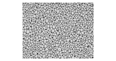
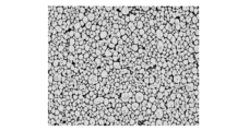
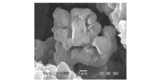
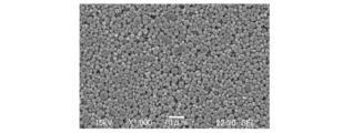
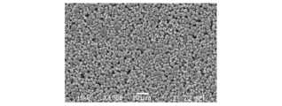
焼結体表面を、走査型電子顕微鏡で撮影した画像を画像解析ソフトで画像処理した後、解析し、焼結体の表面の100μm×115μmの任意の領域内の粒子径1μm以下の粉末の個数を数えることにより測定した。焼結体表面を、走査型電子顕微鏡で撮影し、画像解析ソフトで画像処理した画像を図3~図6に示す。図3は実施例1、図4は実施例2、図5は比較例1、図6は比較例5の画像である。 Images of the sintered body surface taken with a scanning electron microscope were processed with image analysis software, and then analyzed to count the number of powder particles with a particle size of 1 μm or less within an arbitrary region of 100 μm x 115 μm on the surface of the sintered body. Images of the sintered body surface taken with a scanning electron microscope and processed with image analysis software are shown in Figures 3 to 6. Figure 3 is an image of Example 1, Figure 4 is an image of Example 2, Figure 5 is an image of Comparative Example 1, and Figure 6 is an image of Comparative Example 5.
(第3の工程)
製造された電極材に、更に、陽極酸化処理を施した。陽極酸化処理は、化成電圧250~800Vで日本電子機械工業会規格RC-2364Aに従い行った。
(Third step)
The produced electrode material was further subjected to anodizing treatment at a formation voltage of 250 to 800 V in accordance with the Japan Electronics Industries Association standard RC-2364A.
(実施例2~5、比較例1~7)
粉末を表1に示す粉末に変更し、焼結体の厚みを表1に示す厚みに変更した以外は実施1と同様にして電極材を製造し、陽極酸化処理を施した。
(Examples 2 to 5, Comparative Examples 1 to 7)
An electrode material was produced in the same manner as in Example 1, except that the powder was changed to one shown in Table 1 and the thickness of the sintered body was changed to one shown in Table 1, and an anodizing treatment was performed.
なお、参考に、使用粉末A-1及びCの体積基準の粒子径を表2に示す。 For reference, the volumetric particle sizes of powders A-1 and C used are shown in Table 2.
(静電容量評価試験)
日本電子機械工業会規格RC-2364Aに準拠し、各実施例及び比較例の電極材を使用した際の静電容量評価試験を実施した。
(Capacitance evaluation test)
In accordance with the Japan Electronics Industries Association standard RC-2364A, a capacitance evaluation test was carried out when the electrode materials of each of the examples and comparative examples were used.
(折曲強度評価試験)
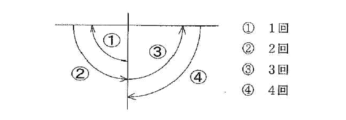
化成処理後の電極材の折り曲げ強度を、日本電子機械工業会規定のMIT型自動折り曲げ試験法(日本電子機械工業会規格RC-2364A)に従って測定した。MIT型自動折り曲げ試験装置はJIS P8115で規定された装置を使用し、折り曲げ回数は、各電極材が破断する折り曲げ回数とし、図7に示すように90°曲げて1回、元に戻して2回、反対方向に90°曲げて3回、元に戻して4回と数え、5回目以降は、1~4回目と同様に折り曲げ操作を、電極材が破断するまで繰り返した。尚、表3における「折曲強度」の欄には、上記操作を行い、電極材が破断するまでに繰り返した折り曲げ操作の回数(折り曲げ回数)を示す。
(Bending strength evaluation test)
The bending strength of the electrode material after the chemical conversion treatment was measured according to the MIT type automatic bending test method (Japan Electronics Industry Association standard RC-2364A) specified by the Japan Electronics Industry Association. The MIT type automatic bending tester used an apparatus specified by JIS P8115, and the number of bendings was the number of bendings at which each electrode material broke. As shown in FIG. 7, the number of bendings was counted as one bending at 90°, two bendings back, three bendings at 90° in the opposite direction, and four bendings back. From the fifth time onwards, the bending operation was repeated in the same manner as the first to fourth bendings until the electrode material broke. The "Bending Strength" column in Table 3 shows the number of bending operations (number of bendings) repeated until the electrode material broke after the above operation.
結果を表3に示す。 The results are shown in Table 3.
表3の結果から、各実施例の電極材は、対応する各比較例の電極材と比べ、コンデンサに要求される静電容量を示すことができ、且つ、優れた折曲強度を有することが確認された。 The results in Table 3 confirm that the electrode materials of each Example are capable of exhibiting the capacitance required for a capacitor and have superior bending strength compared to the corresponding electrode materials of each Comparative Example.
図1に、実施例1及び比較例5で用いた粉末の個数基準の粒度分布を示す。図1では、実施例1で用いた粉末の粒度分布は粒子径が小さい領域(2μm以下)にピークが殆どなく、粒子径が小さい粒子が少ないことが分かった。これに対し、比較例5で用いた粉末の粒度分布は0.81μmの箇所に大きなピークがあり、粒子径が小さい粒子が多いことが分かった。 Figure 1 shows the particle size distribution based on number of the powders used in Example 1 and Comparative Example 5. As shown in Figure 1, the particle size distribution of the powder used in Example 1 has almost no peak in the small particle size region (2 μm or less), indicating that there are few particles with small particle sizes. In contrast, the particle size distribution of the powder used in Comparative Example 5 has a large peak at 0.81 μm, indicating that there are many particles with small particle sizes.
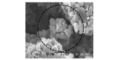
図8~図10に、比較例1により製造し、折曲強度評価試験を行った後の電極材の焼結体の表面をSEM(走査電子顕微鏡)で撮影した画像を示す。図8~図10では、クラックが発生した箇所を撮影している。図8~図10では、微細な粉末が凝集して二次粒子を形成しており、当該二次粒子がクラックの起点となっていることが分かった。また、図8から、二次粒子がクラックの分岐点に影響しているとも考えられる。 Figures 8 to 10 show images taken with a scanning electron microscope (SEM) of the surface of the sintered electrode material manufactured according to Comparative Example 1 after a bending strength evaluation test was conducted. Figures 8 to 10 show images of the locations where cracks occurred. It can be seen from Figures 8 to 10 that the fine powder has aggregated to form secondary particles, and that these secondary particles are the starting points of the cracks. It can also be seen from Figure 8 that the secondary particles affect the branching points of the cracks.
図11及び図12に、実施例1により製造した電極材の焼結体の表面をSEMで撮影した画像を示す。図11及び図12では、焼結体中に微細な粉末が少ないことが分かった。 Figures 11 and 12 show SEM images of the surface of the sintered electrode material produced in Example 1. Figures 11 and 12 show that there is little fine powder in the sintered body.
図13及び図14に、比較例1により製造した電極材の焼結体の表面をSEMで撮影した画像を示す。また、図15及び図16に、比較例4により製造した電極材の焼結体の表面をSEMで撮影した画像を示す。図13~図16では、焼結体中に微細な粉末多く見られることが分かった。 Figures 13 and 14 show SEM images of the surface of the sintered electrode material produced according to Comparative Example 1. Figures 15 and 16 show SEM images of the surface of the sintered electrode material produced according to Comparative Example 4. Figures 13 to 16 show that a large amount of fine powder can be seen in the sintered body.
図17に、実施例1により製造し、折曲強度評価試験にて折り曲げを2回行った後、すなわち、1回折り曲げて戻した後の電極材の焼結体の表面をSEM(走査電子顕微鏡)で撮影した画像を示す。 Figure 17 shows an image taken with a SEM (scanning electron microscope) of the surface of a sintered electrode material manufactured according to Example 1 and after it was bent twice in a bending strength evaluation test, i.e., after it was bent once and then returned to its original shape.
図18に、比較例1により製造し、折曲強度評価試験にて折り曲げを2回行った後の電極材の焼結体の表面をSEM(走査電子顕微鏡)で撮影した画像を示す。 Figure 18 shows an image taken with a SEM (scanning electron microscope) of the surface of a sintered electrode material manufactured according to Comparative Example 1 after bending twice in a bending strength evaluation test.
図19に、比較例5により製造し、折曲強度評価試験にて折り曲げを2回行った後の電極材の焼結体の表面をSEM(走査電子顕微鏡)で撮影した画像を示す。 Figure 19 shows an image taken with a SEM (scanning electron microscope) of the surface of a sintered electrode material manufactured according to Comparative Example 5 after bending twice in a bending strength evaluation test.
図17、図18及び図19の対比により、破断に至るまでの折曲回数に差があるだけでなく、折曲を1回行った時点でクラックの発生に差があり、同じ積層厚みの実施例と比較例とを比較した場合に、実施例は比較例に比べて優れた折曲強度を有していることが分かった。 Comparing Figures 17, 18, and 19, it was found that not only was there a difference in the number of folds required before fracture occurred, but there was also a difference in the occurrence of cracks after one fold, and that when comparing the Examples and Comparative Examples with the same laminate thickness, the Examples had superior fold strength compared to the Comparative Examples.
Claims (5)
(1)前記焼結体の合計厚みは50~900μmであり、
(2)前記焼結体中の粉末の個数基準の粒度分布における10%粒子径D10は1.0~1.8μmであり、
(3)前記焼結体中の粉末の個数基準の粒度分布における50%粒子径D50は2.0~3.5μmであり、
(4)前記焼結体中の粉末の個数基準の粒度分布における90%粒子径D90は3.8~6.0μmである、
ことを特徴とするアルミニウム電解コンデンサ用電極材。 An electrode material for an aluminum electrolytic capacitor having an aluminum foil substrate or an aluminum alloy foil substrate, on at least one surface of which is a sintered body of at least one type of powder selected from the group consisting of aluminum powder and aluminum alloy powder,
(1) the total thickness of the sintered body is 50 to 900 μm;
(2) the 10% particle diameter D10 in the number-based particle size distribution of the powder in the sintered body is 1.0 to 1.8 μm;
(3) the 50% particle diameter D50 in the number-based particle size distribution of the powder in the sintered body is 2.0 to 3.5 μm;
(4) The 90% particle diameter D90 in the number-based particle size distribution of the powder in the sintered body is 3.8 to 6.0 μm;
Electrode material for aluminum electrolytic capacitors.
(2)前記皮膜を560℃以上660℃以下の温度で焼結する第2工程を含み、
前記粉末は、個数基準の粒度分布における10%粒子径D10が1.0~1.8μmであり、個数基準の粒度分布における50%粒子径D50が2.0~3.5μmであり、個数基準の粒度分布における90%粒子径D90が3.8~6.0μmである、
ことを特徴とするアルミニウム電解コンデンサ用電極材の製造方法。 (1) a first step of forming a coating of a paste composition containing at least one powder selected from the group consisting of aluminum powder and aluminum alloy powder on at least one surface of an aluminum foil substrate or an aluminum alloy foil substrate; and (2) a second step of sintering the coating at a temperature of 560° C. or higher and 660° C. or lower.
The powder has a 10% particle diameter D10 in a number-based particle size distribution of 1.0 to 1.8 μm, a 50% particle diameter D50 in a number-based particle size distribution of 2.0 to 3.5 μm, and a 90% particle diameter D90 in a number-based particle size distribution of 3.8 to 6.0 μm.
2. The method for producing an electrode material for an aluminum electrolytic capacitor, comprising the steps of:
Priority Applications (5)
| Application Number | Priority Date | Filing Date | Title |
|---|---|---|---|
| JP2021018442A JP7635010B2 (en) | 2021-02-08 | 2021-02-08 | Electrode material for aluminum electrolytic capacitor and method for producing same |
| EP22749586.8A EP4290545A4 (en) | 2021-02-08 | 2022-01-26 | ELECTRODE MATERIAL FOR ALUMINUM ELECTROLYTIC CAPACITORS AND PROCESS FOR PRODUCING THE SAME |
| PCT/JP2022/002945 WO2022168712A1 (en) | 2021-02-08 | 2022-01-26 | Electrode material for aluminum electrolytic capacitors and method for producing same |
| US18/275,835 US12234559B2 (en) | 2021-02-08 | 2022-01-26 | Electrode material for aluminum electrolytic capacitors and method for producing same |
| CN202280012314.6A CN116848604A (en) | 2021-02-08 | 2022-01-26 | Electrode material for aluminum electrolytic capacitor and manufacturing method thereof |
Applications Claiming Priority (1)
| Application Number | Priority Date | Filing Date | Title |
|---|---|---|---|
| JP2021018442A JP7635010B2 (en) | 2021-02-08 | 2021-02-08 | Electrode material for aluminum electrolytic capacitor and method for producing same |
Publications (2)
| Publication Number | Publication Date |
|---|---|
| JP2022121214A JP2022121214A (en) | 2022-08-19 |
| JP7635010B2 true JP7635010B2 (en) | 2025-02-25 |
Family
ID=82741494
Family Applications (1)
| Application Number | Title | Priority Date | Filing Date |
|---|---|---|---|
| JP2021018442A Active JP7635010B2 (en) | 2021-02-08 | 2021-02-08 | Electrode material for aluminum electrolytic capacitor and method for producing same |
Country Status (5)
| Country | Link |
|---|---|
| US (1) | US12234559B2 (en) |
| EP (1) | EP4290545A4 (en) |
| JP (1) | JP7635010B2 (en) |
| CN (1) | CN116848604A (en) |
| WO (1) | WO2022168712A1 (en) |
Citations (3)
| Publication number | Priority date | Publication date | Assignee | Title |
|---|---|---|---|---|
| EP1818956A2 (en) | 2006-02-09 | 2007-08-15 | Cerel (Ceramic Technologies) Ltd. | High capacitance capacitor anode |
| JP2012221855A (en) | 2011-04-12 | 2012-11-12 | Sony Corp | Positive electrode active material for nonaqueous electrolyte battery, positive electrode for nonaqueous electrolyte battery, and nonaqueous electrolyte battery, and battery pack, electronic device, electric vehicle, power storage device, and electric power system comprising nonaqueous electrolyte battery |
| WO2015098644A1 (en) | 2013-12-27 | 2015-07-02 | 東洋アルミニウム株式会社 | Electrode foil for aluminum electrolytic capacitor and production method for same |
Family Cites Families (13)
| Publication number | Priority date | Publication date | Assignee | Title |
|---|---|---|---|---|
| JP2000277368A (en) * | 1999-03-23 | 2000-10-06 | Matsushita Electric Ind Co Ltd | Multilayer ceramic capacitor |
| WO2003008673A1 (en) * | 2001-07-18 | 2003-01-30 | Showa Denko Kabushiki Kaisha | Metal foil consisting of alloy of earth-acid metal, and capacitor provided with the same |
| JP4958510B2 (en) * | 2006-10-10 | 2012-06-20 | 東洋アルミニウム株式会社 | Electrode material for aluminum electrolytic capacitor and method for producing the same |
| US8043532B2 (en) * | 2007-11-22 | 2011-10-25 | Cheil Industries Inc. | Composition for electrodes comprising aluminum powder having controlled particle size distribution and size, and electrodes made using the same |
| KR20090053667A (en) * | 2007-11-22 | 2009-05-27 | 제일모직주식회사 | Electrode forming composition comprising aluminum powder with controlled particle size distribution and size and electrode manufactured using the same |
| JP5160321B2 (en) * | 2008-06-27 | 2013-03-13 | 株式会社ノリタケカンパニーリミテド | Silicon solar cell manufacturing method and aluminum paste used in the manufacturing method |
| JP5614960B2 (en) * | 2009-09-03 | 2014-10-29 | 東洋アルミニウム株式会社 | Porous aluminum material with improved bending strength and method for producing the same |
| US9378897B2 (en) * | 2011-05-26 | 2016-06-28 | Toyo Aluminium Kabushiki Kaisha | Electrode material for aluminum electrolytic capacitor, and process for producing same |
| JP6143472B2 (en) * | 2013-01-18 | 2017-06-07 | 東洋アルミニウム株式会社 | Manufacturing method of electrode material for aluminum electrolytic capacitor and electrode material for aluminum electrolytic capacitor. |
| WO2016136804A1 (en) | 2015-02-27 | 2016-09-01 | 東洋アルミニウム株式会社 | Electrode material for aluminum electrolytic capacitors and method for producing same |
| JP6683243B2 (en) * | 2016-03-07 | 2020-04-15 | 株式会社村田製作所 | Method for manufacturing bonded body and bonding material |
| JP6762848B2 (en) * | 2016-11-02 | 2020-09-30 | 東洋アルミニウム株式会社 | Paste composition |
| JP6953265B2 (en) * | 2017-10-10 | 2021-10-27 | 東洋アルミニウム株式会社 | Electrode material for aluminum electrolytic capacitors and its manufacturing method |
-
2021
- 2021-02-08 JP JP2021018442A patent/JP7635010B2/en active Active
-
2022
- 2022-01-26 CN CN202280012314.6A patent/CN116848604A/en active Pending
- 2022-01-26 WO PCT/JP2022/002945 patent/WO2022168712A1/en not_active Ceased
- 2022-01-26 US US18/275,835 patent/US12234559B2/en active Active
- 2022-01-26 EP EP22749586.8A patent/EP4290545A4/en active Pending
Patent Citations (3)
| Publication number | Priority date | Publication date | Assignee | Title |
|---|---|---|---|---|
| EP1818956A2 (en) | 2006-02-09 | 2007-08-15 | Cerel (Ceramic Technologies) Ltd. | High capacitance capacitor anode |
| JP2012221855A (en) | 2011-04-12 | 2012-11-12 | Sony Corp | Positive electrode active material for nonaqueous electrolyte battery, positive electrode for nonaqueous electrolyte battery, and nonaqueous electrolyte battery, and battery pack, electronic device, electric vehicle, power storage device, and electric power system comprising nonaqueous electrolyte battery |
| WO2015098644A1 (en) | 2013-12-27 | 2015-07-02 | 東洋アルミニウム株式会社 | Electrode foil for aluminum electrolytic capacitor and production method for same |
Also Published As
| Publication number | Publication date |
|---|---|
| JP2022121214A (en) | 2022-08-19 |
| EP4290545A4 (en) | 2025-01-29 |
| CN116848604A (en) | 2023-10-03 |
| US12234559B2 (en) | 2025-02-25 |
| US20240301561A1 (en) | 2024-09-12 |
| EP4290545A1 (en) | 2023-12-13 |
| WO2022168712A1 (en) | 2022-08-11 |
Similar Documents
| Publication | Publication Date | Title |
|---|---|---|
| JP5769528B2 (en) | Electrode material for aluminum electrolytic capacitor and method for producing the same | |
| CN102017034B (en) | Electrode material for aluminum electrolytic capacitor and method of manufacturing same | |
| TWI544509B (en) | Electrode for electrolytic capacitor for electrolysis and method for manufacturing the same | |
| JP5511630B2 (en) | Electrode material for aluminum electrolytic capacitor and method for producing the same | |
| US20110053764A1 (en) | Porous aluminum material having improved bending strength and production method therefor | |
| JP2008098279A (en) | Electrode material for aluminum electrolytic capacitor and method for producing the same | |
| JP6073255B2 (en) | Method for producing electrode material for aluminum electrolytic capacitor | |
| JP5618714B2 (en) | Electrode material for aluminum electrolytic capacitor and method for producing the same | |
| JP6629288B2 (en) | Electrode material for aluminum electrolytic capacitor and method for producing the same | |
| WO2019073616A1 (en) | Electrode material for aluminum electrolytic capacitors and method for producing same | |
| JP7635010B2 (en) | Electrode material for aluminum electrolytic capacitor and method for producing same | |
| JP2018206910A (en) | Electrode material for aluminum electrolytic capacitor and method for producing the same | |
| US20240120154A1 (en) | Electrode material for aluminum electrolytic capacitors and method for producing same | |
| WO2016158492A1 (en) | Electrode material for aluminum electrolytic capacitor and method for manufacturing same |
Legal Events
| Date | Code | Title | Description |
|---|---|---|---|
| A621 | Written request for application examination |
Free format text: JAPANESE INTERMEDIATE CODE: A621 Effective date: 20231110 |
|
| TRDD | Decision of grant or rejection written | ||
| A01 | Written decision to grant a patent or to grant a registration (utility model) |
Free format text: JAPANESE INTERMEDIATE CODE: A01 Effective date: 20250114 |
|
| A61 | First payment of annual fees (during grant procedure) |
Free format text: JAPANESE INTERMEDIATE CODE: A61 Effective date: 20250212 |
|
| R150 | Certificate of patent or registration of utility model |
Ref document number: 7635010 Country of ref document: JP Free format text: JAPANESE INTERMEDIATE CODE: R150 |
|
| S111 | Request for change of ownership or part of ownership |
Free format text: JAPANESE INTERMEDIATE CODE: R313113 |
|
| R350 | Written notification of registration of transfer |
Free format text: JAPANESE INTERMEDIATE CODE: R350 |