JP7634026B2 - PIXEL ARRAY STRUCTURE, DISPLAY PANEL AND DISPLAY DEVICE - Google Patents
PIXEL ARRAY STRUCTURE, DISPLAY PANEL AND DISPLAY DEVICE Download PDFInfo
- Publication number
- JP7634026B2 JP7634026B2 JP2022580483A JP2022580483A JP7634026B2 JP 7634026 B2 JP7634026 B2 JP 7634026B2 JP 2022580483 A JP2022580483 A JP 2022580483A JP 2022580483 A JP2022580483 A JP 2022580483A JP 7634026 B2 JP7634026 B2 JP 7634026B2
- Authority
- JP
- Japan
- Prior art keywords
- pixel
- sub
- subpixel
- center
- unit
- Prior art date
- Legal status (The legal status is an assumption and is not a legal conclusion. Google has not performed a legal analysis and makes no representation as to the accuracy of the status listed.)
- Active
Links
Images


Classifications
-
- H—ELECTRICITY
- H10—SEMICONDUCTOR DEVICES; ELECTRIC SOLID-STATE DEVICES NOT OTHERWISE PROVIDED FOR
- H10K—ORGANIC ELECTRIC SOLID-STATE DEVICES
- H10K59/00—Integrated devices, or assemblies of multiple devices, comprising at least one organic light-emitting element covered by group H10K50/00
- H10K59/30—Devices specially adapted for multicolour light emission
- H10K59/35—Devices specially adapted for multicolour light emission comprising red-green-blue [RGB] subpixels
- H10K59/353—Devices specially adapted for multicolour light emission comprising red-green-blue [RGB] subpixels characterised by the geometrical arrangement of the RGB subpixels
-
- G—PHYSICS
- G09—EDUCATION; CRYPTOGRAPHY; DISPLAY; ADVERTISING; SEALS
- G09G—ARRANGEMENTS OR CIRCUITS FOR CONTROL OF INDICATING DEVICES USING STATIC MEANS TO PRESENT VARIABLE INFORMATION
- G09G3/00—Control arrangements or circuits, of interest only in connection with visual indicators other than cathode-ray tubes
- G09G3/20—Control arrangements or circuits, of interest only in connection with visual indicators other than cathode-ray tubes for presentation of an assembly of a number of characters, e.g. a page, by composing the assembly by combination of individual elements arranged in a matrix no fixed position being assigned to or needed to be assigned to the individual characters or partial characters
-
- G—PHYSICS
- G09—EDUCATION; CRYPTOGRAPHY; DISPLAY; ADVERTISING; SEALS
- G09G—ARRANGEMENTS OR CIRCUITS FOR CONTROL OF INDICATING DEVICES USING STATIC MEANS TO PRESENT VARIABLE INFORMATION
- G09G5/00—Control arrangements or circuits for visual indicators common to cathode-ray tube indicators and other visual indicators
- G09G5/02—Control arrangements or circuits for visual indicators common to cathode-ray tube indicators and other visual indicators characterised by the way in which colour is displayed
- G09G5/04—Control arrangements or circuits for visual indicators common to cathode-ray tube indicators and other visual indicators characterised by the way in which colour is displayed using circuits for interfacing with colour displays
-
- H—ELECTRICITY
- H10—SEMICONDUCTOR DEVICES; ELECTRIC SOLID-STATE DEVICES NOT OTHERWISE PROVIDED FOR
- H10K—ORGANIC ELECTRIC SOLID-STATE DEVICES
- H10K59/00—Integrated devices, or assemblies of multiple devices, comprising at least one organic light-emitting element covered by group H10K50/00
- H10K59/30—Devices specially adapted for multicolour light emission
- H10K59/35—Devices specially adapted for multicolour light emission comprising red-green-blue [RGB] subpixels
- H10K59/351—Devices specially adapted for multicolour light emission comprising red-green-blue [RGB] subpixels comprising more than three subpixels, e.g. red-green-blue-white [RGBW]
-
- H—ELECTRICITY
- H10—SEMICONDUCTOR DEVICES; ELECTRIC SOLID-STATE DEVICES NOT OTHERWISE PROVIDED FOR
- H10K—ORGANIC ELECTRIC SOLID-STATE DEVICES
- H10K59/00—Integrated devices, or assemblies of multiple devices, comprising at least one organic light-emitting element covered by group H10K50/00
- H10K59/30—Devices specially adapted for multicolour light emission
- H10K59/35—Devices specially adapted for multicolour light emission comprising red-green-blue [RGB] subpixels
- H10K59/352—Devices specially adapted for multicolour light emission comprising red-green-blue [RGB] subpixels the areas of the RGB subpixels being different
-
- H—ELECTRICITY
- H10—SEMICONDUCTOR DEVICES; ELECTRIC SOLID-STATE DEVICES NOT OTHERWISE PROVIDED FOR
- H10K—ORGANIC ELECTRIC SOLID-STATE DEVICES
- H10K59/00—Integrated devices, or assemblies of multiple devices, comprising at least one organic light-emitting element covered by group H10K50/00
- H10K59/80—Constructional details
- H10K59/875—Arrangements for extracting light from the devices
- H10K59/876—Arrangements for extracting light from the devices comprising a resonant cavity structure, e.g. Bragg reflector pair
Landscapes
- Engineering & Computer Science (AREA)
- Physics & Mathematics (AREA)
- Computer Hardware Design (AREA)
- General Physics & Mathematics (AREA)
- Theoretical Computer Science (AREA)
- Devices For Indicating Variable Information By Combining Individual Elements (AREA)
- Electroluminescent Light Sources (AREA)
- Liquid Crystal (AREA)
Description
本発明は、表示技術分野に関し、特に画素配列構造、表示パネル及び表示装置に関する。 The present invention relates to the field of display technology, and in particular to a pixel array structure, a display panel, and a display device.
本出願は、2020年07月01日に中国特許庁に出願された2020106221094という出願番号である「画素配列構造、表示パネル及び表示装置」の特許出願、2020年07月01日に中国特許庁に出願された2020106221107という出願番号である「画素配列構造、表示パネル及び表示装置」の特許出願、及び2020年07月01日に中国特許庁に出願された2020106220956という出願番号である「画素配列構造、表示パネル及び表示装置」の特許出願に基づいて優先権を主張し、その内容はすべて参照により本明細書に組み込まれる。 This application claims priority to the patent application for "Pixel array structure, display panel and display device" filed with the China Patent Office on July 1, 2020, with application number 2020106221094, the patent application for "Pixel array structure, display panel and display device" filed with the China Patent Office on July 1, 2020, with application number 2020106221107, and the patent application for "Pixel array structure, display panel and display device" filed with the China Patent Office on July 1, 2020, with application number 2020106220956, the contents of which are all incorporated herein by reference.
表示技術の発展に伴い、表示パネルの解像度に対する要求も高まっている。表示品質が高いなどの利点があるため、高解像度表示パネルの応用範囲もますます広くなってきている。通常、サブ画素のサイズの低減やサブ画素間の間隔の低減により、表示装置の解像度を向上させることができる。しかしながら、サブ画素のサイズとサブ画素間の間隔の低減により製造プロセスの精度に対する要求もますます高くなり、それによって表示装置の製造プロセスの難しさ及び製造コストが増加する。 As display technology develops, the demand for resolution of display panels is also increasing. Due to advantages such as high display quality, the range of applications of high-resolution display panels is becoming increasingly wider. Typically, the resolution of a display device can be improved by reducing the size of the subpixels and the spacing between the subpixels. However, the reduction in the size of the subpixels and the spacing between the subpixels also increases the demand for precision in the manufacturing process, thereby increasing the difficulty and manufacturing costs of the display device manufacturing process.
サブピクセルレンダリング(Sup-PixeL Rendering,SPR)技術は人間の目による異なる色のサブ画素の解像度の違いを利用して、赤、緑、青の三色サブ画素によって1つの画素を簡単に定義する従来のモードを変更し、異なる画素間で特定の位置の解像度の鈍感な色のサブ画素を共有し、相対的に少ないサブ画素を用いて、同じ画素解像度の表現能力をシミュレーションして実現することにより、製造プロセスの難しさと製造コストを低減させる。 Sub-pixel rendering (SPR) technology utilizes the difference in resolution of sub-pixels of different colors as perceived by the human eye, changing the conventional mode of simply defining one pixel with three sub-pixels of red, green, and blue colors, and instead shares sub-pixels of colors with low resolution at specific positions between different pixels, simulating and realizing the expressive ability of the same pixel resolution using relatively fewer sub-pixels, thereby reducing the difficulty and cost of the manufacturing process.
これに基づいて、高解像度を実現するとともに、カラーエッジ現象及び表示効果を効果的に改善することができる画素配列構造、表示パネル及び表示装置を提供する必要がある。 Based on this, it is necessary to provide a pixel array structure, a display panel, and a display device that can achieve high resolution and effectively improve the color edge phenomenon and display effect.
本発明の第1様態によれば、複数の第1画素ユニットと複数の第2画素ユニットを含む画素配列構造であって、複数の前記第1画素ユニットと複数の前記第2画素ユニットは第1方向及び第2方向に交互に配列され、各前記第1画素ユニットと前記第2画素ユニットはいずれも第1サブ画素、第2サブ画素、第3サブ画素及び第4サブ画素を含み、前記第1サブ画素は前記第3サブ画素の中心と前記第4サブ画素の中心を結ぶ連結線の一側に位置し、前記第2サブ画素は前記第3サブ画素の中心と前記第4サブ画素の中心を結ぶ連結線の他側に位置し、所定角度だけ回転した前記第2画素ユニットのサブ画素配列構造は、前記第1画素ユニットのサブ画素配列構造と鏡像対称であり、前記所定角度は0°よりも大きく且つ360°未満である画素配列構造が提供される。 According to a first aspect of the present invention, there is provided a pixel array structure including a plurality of first pixel units and a plurality of second pixel units, the plurality of first pixel units and the plurality of second pixel units are alternately arranged in a first direction and a second direction, each of the first pixel units and the second pixel units includes a first sub-pixel, a second sub-pixel, a third sub-pixel and a fourth sub-pixel, the first sub-pixel is located on one side of a connecting line connecting the center of the third sub-pixel to the center of the fourth sub-pixel, and the second sub-pixel is located on the other side of a connecting line connecting the center of the third sub-pixel to the center of the fourth sub-pixel, and the sub-pixel array structure of the second pixel unit rotated by a predetermined angle is mirror-symmetrical to the sub-pixel array structure of the first pixel unit, and the predetermined angle is greater than 0° and less than 360°.
上記の画素配列構造では、所定角度だけ回転した第2画素ユニットのサブ画素配列構造が第1画素ユニットにおけるサブ画素配列構造と鏡像対称であることにより、サブ画素の配列の緊密さ及びサブ画素間の間隔を両立し、両者の間にバランスを取ることができ、高解像度を有すると同時に、色のにじみのリスクや色ずれの低減、カラーエッジや視覚的な粒状感の改善に寄与する。 In the above pixel array structure, the subpixel array structure of the second pixel unit rotated by a predetermined angle is a mirror image of the subpixel array structure of the first pixel unit, which allows for both a tightly packed array of subpixels and a good spacing between the subpixels, achieving a balance between the two, thereby achieving high resolution while also reducing the risk of color bleeding and color shifts and improving color edges and visual graininess.
本発明の第2様態によれば、第1画素ユニットを含む画素配列構造であって、前記第1画素ユニットは、第1サブ画素、第2サブ画素、第3サブ画素及び第4サブ画素を含み、前記第1画素ユニット内において、前記第1サブ画素、前記第2サブ画素、前記第3サブ画素及び前記第4サブ画素のそれぞれの中心を頂点として面積が重なり合わない辺を共有する三角形を構成し、且つ、前記第1サブ画素の中心と前記第2サブ画素の中心を前記辺を共有する三角形の共有辺の頂点とし、前記第2サブ画素は第2長軸及び第2短軸を有し、前記第1画素ユニット内において、前記第2サブ画素の長軸方向に沿う中心線は、前記第3サブ画素及び/又は前記第4サブ画素の中心を通過しない画素配列構造が提供される。 According to a second aspect of the present invention, there is provided a pixel array structure including a first pixel unit, the first pixel unit including a first sub-pixel, a second sub-pixel, a third sub-pixel, and a fourth sub-pixel, in which the first sub-pixel, the second sub-pixel, the third sub-pixel, and the fourth sub-pixel form a triangle with a shared side that does not overlap in area, with the center of the first sub-pixel and the center of the second sub-pixel being the vertex of the shared side of the triangle, the second sub-pixel has a second major axis and a second minor axis, and in the first pixel unit, a center line along the major axis direction of the second sub-pixel does not pass through the center of the third sub-pixel and/or the fourth sub-pixel.
本発明の第3様態によれば、第1サブ画素、第2サブ画素、第3サブ画素及び第4サブ画素を含む画素配列構造であって、アライメントして設置された2つの前記第1サブ画素の中心、及びアライメントして設置された2つの前記第2サブ画素の中心を頂点として結んで仮想四角形を形成し、前記仮想四角形は対向設置された2つの等辺、対向設置され等辺の頂点を繋げる短辺及び長辺を含み、前記仮想四角形の短辺と前記仮想四角形の長辺は平行ではなく、前記仮想四角形には1つの第3サブ画素又は1つの第4サブ画素が配置され、前記第3サブ画素と前記第4サブ画素は同じ色で発光する画素配列構造が提供される。 According to a third aspect of the present invention, there is provided a pixel array structure including a first sub-pixel, a second sub-pixel, a third sub-pixel, and a fourth sub-pixel, in which a virtual rectangle is formed by connecting the centers of two aligned first sub-pixels and the centers of two aligned second sub-pixels as vertices, the virtual rectangle includes two equal sides arranged opposite each other, and a short side and a long side connecting the vertices of the equal sides arranged opposite each other, the short side of the virtual rectangle and the long side of the virtual rectangle are not parallel, one third sub-pixel or one fourth sub-pixel is arranged in the virtual rectangle, and the third sub-pixel and the fourth sub-pixel emit light of the same color.
本発明の第4様態によれば、本発明の上記第1乃至第3様態に記載の画素配列構造を含む表示パネルが提供される。 According to a fourth aspect of the present invention, there is provided a display panel including a pixel array structure according to any one of the first to third aspects of the present invention.
本発明の第5様態によれば、本発明の第4様態に記載の表示パネルを含む表示装置が提供される。 According to a fifth aspect of the present invention, there is provided a display device including the display panel according to the fourth aspect of the present invention.
本発明の理解を容易にするために、以下に関連する図面を参照して本発明をより全面的に説明する。図面には本発明の好ましい実施例が示されている。しかし、本発明は多くの異なる形態で実現することができ、本明細書に記載される実施例に限定されるものではない。逆に、これらの実施例を提供する目的としては、本発明の開示内容をより徹底的且つ包括的に理解することである。 In order to facilitate an understanding of the present invention, the present invention will now be described more fully with reference to the associated drawings, in which preferred embodiments of the present invention are shown. However, the present invention may be embodied in many different forms and is not limited to the embodiments set forth herein. On the contrary, the purpose of providing these embodiments is to provide a more thorough and comprehensive understanding of the present disclosure.
理解すべきこととして、本明細書では用語「第1」、「第2」等を用いて各種類の素子を説明することができるが、何ら順次、数又は重要性を表すものではなく、異なる組成部分を区分するために用いるに過ぎない。これらの用語は、単に一方の素子と他方の素子とを区分するためのものであるに過ぎない。例えば、本発明の範囲から逸脱することなく、第1素子は第2素子と称されてもよく、同様に、第2素子は第1素子と称されても良い。「含む」又は「含み」などの単語は、当該単語の前に現れる素子またはオブジェクトが、当該単語の後に現れる例示な素子またはオブジェクトおよびそれらの同等物をカバーし、他の素子またはオブジェクトを除外しないという意味である。 It should be understood that the terms "first", "second", etc. may be used herein to describe each type of element, but do not denote any sequentiality, number, or importance, but are merely used to distinguish different compositional parts. These terms are merely used to distinguish one element from another. For example, a first element may be referred to as a second element, and similarly, a second element may be referred to as a first element, without departing from the scope of the present invention. Words such as "comprises" or "including" mean that the elements or objects appearing before the word cover the exemplary elements or objects appearing after the word and their equivalents, and do not exclude other elements or objects.
OLED表示パネルは電流によって駆動されるものであり、OLEDデバイスが発光するように、OLEDデバイスに接続された画素駆動回路を提供して、OLEDデバイスへ駆動電流を提供する必要がある。OLEDデバイスは、少なくともアノード、カソード、及びアノードとカソードとの間に位置する有機発光材料を含む。上面発光型OLED表示パネルを例にとると、有機発光材料は安定性が低いため、従来のエッチングプロセスを用いてパターン化を行うことができず、代わりにマスク板による蒸着プロセスを用いてパターン化を行う。有機発光材料を真空環境に置き、加熱により有機材料を蒸発又は昇華させる。有機材料を蒸発させるチャンバと蒸着対象であるアレイ基板との間にはマスク板が設けられ、マスク板には蒸着必要がある領域に対応する開口部が設けられ、蒸着の必要がない領域には開口部が設けられていない。蒸発又は昇華した有機材料分子は開口部を介して蒸着対象であるアレイ基板に付着し、それによってパターン化された有機材料層を直接形成する。各サブ画素の発光材料層を対応して蒸着するマスク板は、ファインマスクと略称されるファインメタルマスク(FMM,Fine MetaL Mask)である。ファインマスクの開口部の寸法、開口部間の間隔の寸法の制限及び引っ張りの難しさに制限されるため、関連技術の画素配列によって有機発光表示パネルの画素密度(PPI,pixeL per inch,以下、画素密度と称される)をさらに向上させることができない。 The OLED display panel is driven by current, and it is necessary to provide a pixel driving circuit connected to the OLED device to provide a driving current to the OLED device so that the OLED device emits light. The OLED device includes at least an anode, a cathode, and an organic light-emitting material located between the anode and the cathode. Taking a top-emitting OLED display panel as an example, the organic light-emitting material has low stability, so it cannot be patterned using a conventional etching process, and instead is patterned using a deposition process using a mask plate. The organic light-emitting material is placed in a vacuum environment, and the organic material is evaporated or sublimated by heating. A mask plate is provided between the chamber for evaporating the organic material and the array substrate to be evaporated, and the mask plate has openings corresponding to the areas that need to be evaporated, and no openings are provided in the areas that do not need to be evaporated. The evaporated or sublimated organic material molecules are attached to the array substrate to be evaporated through the openings, thereby directly forming a patterned organic material layer. The mask plate for depositing the light-emitting material layer of each subpixel is a fine metal mask (FMM), abbreviated as fine mask. Due to the limitations of the size of the openings of the fine mask, the size of the gap between the openings, and the difficulty of stretching, the pixel density (PPI, pixel per inch, hereinafter referred to as pixel density) of the organic light-emitting display panel cannot be further improved by the pixel arrangement of the related art.
上記の課題を解決するために、関連技術では、サブピクセルレンダリング技術(SPR,Sub PixeL Rendering)を用いて表示パネルの解像度を向上させる。図1に示すように、非レンダリングの場合、画素は3つのサブ画素を含む一方、レンダリングの場合、画素は、2つのサブ画素のみを含むので、サブ画素を変更することなく、画素の数を50%向上させ、さらに解像度を向上させる。しかしながら、サブピクセルレンダリング技術において、各画素は2つのサブ画素のみを含み、フルカラー表示を実現するために、隣のサブ画素からそれが表示できない色を借用する必要がある。そのため、このような画素配列構造で表示する場合には、行方向及び/又は列方向において各色のサブ画素の数の違いや、エッジを表示するサブ画素の突出度合いの違いによって、画面のエッジでカラーエッジが発生し、表示品質に影響を与えることがある。 To solve the above problem, the related art uses a sub-pixel rendering technique (SPR, Sub Pixel Rendering) to improve the resolution of a display panel. As shown in FIG. 1, in the case of non-rendering, a pixel includes three sub-pixels, while in the case of rendering, a pixel includes only two sub-pixels, so that the number of pixels is increased by 50% without changing the sub-pixels, and the resolution is further improved. However, in the sub-pixel rendering technique, each pixel includes only two sub-pixels, and in order to realize a full-color display, it is necessary to borrow a color that it cannot display from an adjacent sub-pixel. Therefore, when displaying with such a pixel array structure, a color edge may occur at the edge of the screen due to the difference in the number of sub-pixels of each color in the row direction and/or column direction, or the difference in the protrusion degree of the sub-pixel that displays the edge, which may affect the display quality.
それと同時に、表示パネルがよい発光効果を具備させるために、サブ画素をより均一に配列し、隣接する同一色のサブ画素を1つのマスク板の開口部を共有するように設計して、マスク板の開口部の面積を大きくし、位置合わせの難しさを低減させることが期待されている。しかし、このような画素配列構造を採用する表示パネルは、表示する際に、人間の目によって隣接する同一色のサブ画素を明確に区別することが難しく、視覚的に2つを1つに融合させる状況が生じて粒状感を生み出し、表示品質に影響を与える。 At the same time, in order to provide a display panel with a good light-emitting effect, it is expected that the subpixels can be arranged more uniformly and adjacent subpixels of the same color can be designed to share an opening in one mask plate, thereby increasing the area of the opening in the mask plate and reducing the difficulty of alignment. However, when a display panel employs such a pixel arrangement structure, it is difficult for the human eye to clearly distinguish adjacent subpixels of the same color during display, resulting in a situation where the two are visually merged into one, creating a grainy feeling and affecting the display quality.
また、端末装置の機能をより多く発揮させるために、画面下表示領域に感光デバイスを設けることが広くなっており、例えば、画面下の表示領域に指紋認識デバイスを設ける。ここで、指紋認識デバイスは、指紋画像取得用の感光デバイスを含み、当該感光デバイスは、光学センサを含み、光学センサは、複数の画素点を含み、当該複数の画素点は、物体の異なる位置で反射する光信号をそれぞれ受信し、受信した光信号を電信号に変換して、物体の画像を生成することができる。従って、画素点によって受信した光信号の光量及びコントラストはいずれも生成された物体の画像品質に影響を与える。このようにして、表示パネルの光透過性についても一定の要求があり、さらに画素配列構造の設計に難しさをもたらす。 In addition, in order to provide more functions of the terminal device, it is becoming common to provide a photosensitive device in the display area under the screen, for example, a fingerprint recognition device is provided in the display area under the screen. Here, the fingerprint recognition device includes a photosensitive device for acquiring a fingerprint image, the photosensitive device includes an optical sensor, and the optical sensor includes a plurality of pixel points, which respectively receive optical signals reflected at different positions of an object, and convert the received optical signals into electrical signals to generate an image of the object. Therefore, both the light quantity and contrast of the optical signals received by the pixel points affect the image quality of the generated object. In this way, there are certain requirements for the light transmittance of the display panel, which further brings difficulties in designing the pixel array structure.
上記の課題を解決するために、本発明の実施例では、上記の課題をよりよく改善することができる画素配列構造、表示パネル及び表示装置が提供される。 In order to solve the above problems, the embodiments of the present invention provide a pixel array structure, a display panel, and a display device that can better improve the above problems.
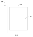
図2は本発明の一実施例における表示パネルの構造概略図を示す。 Figure 2 shows a schematic diagram of the display panel structure in one embodiment of the present invention.
図面を参照して、本発明の少なくとも一実施例における表示パネル100は、表示領域10及び非表示領域20を含み、表示領域10は複数のサブ画素により画像を表示する。具体的には、表示領域10は矩形であってもよく、非表示領域20は表示領域10を囲むように設けられる。もちろん、表示領域10及び非表示領域20の形状及びレイアウトは上述した例示を含むが、これらに限定されない。例えば、表示パネル100がユーザに装着されたウェアラブル機器(例えば腕時計)に用いられる場合、表示領域10は円形形状を有してもよい。表示基板が車両に用いられて表示する場合、表示領域10及び非表示領域20は、例えば円形、多角形又は他の形状を採用してもよい。表示領域10には異なる色の光を発する複数のサブ画素が設けられ、サブ画素とは光を発するための最小ユニット(例えば、表示パネル100の最小アドレス可能なユニット)という意味である。
With reference to the drawings, the
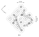
図3は本発明の一実施例における第1画素ユニットの配列概略図を示し、図4は本発明の一実施例における第2画素ユニットの配列概略図を示す。図5は本発明の一実施例における重複ユニットの画素配列概略図を示し、図6は本発明の一実施例における表示マトリックスの配列概略図を示す。図7は本発明の一実施例における画素配列構造の部分構造概略図である。 Figure 3 shows a schematic diagram of the arrangement of a first pixel unit in one embodiment of the present invention, and Figure 4 shows a schematic diagram of the arrangement of a second pixel unit in one embodiment of the present invention. Figure 5 shows a schematic diagram of the pixel arrangement of an overlapping unit in one embodiment of the present invention, and Figure 6 shows a schematic diagram of the arrangement of a display matrix in one embodiment of the present invention. Figure 7 is a schematic diagram of a partial structure of a pixel array structure in one embodiment of the present invention.
具体的には、図3乃至図7を参照すると、本発明の第1様態では画素配列構造が提供される。 Specifically, referring to Figures 3 to 7, a pixel array structure is provided in a first embodiment of the present invention.
本発明の第1様態によれば、本発明の少なくとも一実施例における画素配列構造は、複数の第1画素ユニット及び複数の第2画素ユニットを含む。第1画素ユニット及び第2画素ユニットは互いに隣接し、且つ複数の第1画素ユニットと複数の第2画素ユニットは第1方向及び第2方向に交互に配列される。例えば、図5及び図6に示すように、第1方向は図中のX方向であり、第2方向は図中のY方向である。第1方向において、第1画素ユニット及び第2画素ユニットは交互に配列され、第2方向において、第1画素ユニット及び第2画素ユニットは交互に配列される。つまり、第1方向及び第2方向において、任意の2つの隣接する第1画素ユニットは1つの第2画素ユニットによって隔離され、任意の2つの隣接する第2画素ユニットは1つの第1画素ユニットによって隔離される。具体的な実施形態として、第1方向は行方向との夾角が45°であり、第2方向は第1方向に対して垂直であり、列方向との夾角が45°である。このようにして、サブ画素をコンパクトに配列し、スペースを十分に利用して、開口率を向上させる。 According to a first aspect of the present invention, a pixel array structure in at least one embodiment of the present invention includes a plurality of first pixel units and a plurality of second pixel units. The first pixel units and the second pixel units are adjacent to each other, and the plurality of first pixel units and the plurality of second pixel units are alternately arranged in a first direction and a second direction. For example, as shown in FIG. 5 and FIG. 6, the first direction is the X direction in the figure, and the second direction is the Y direction in the figure. In the first direction, the first pixel units and the second pixel units are alternately arranged, and in the second direction, the first pixel units and the second pixel units are alternately arranged. That is, in the first direction and the second direction, any two adjacent first pixel units are separated by one second pixel unit, and any two adjacent second pixel units are separated by one first pixel unit. In a specific embodiment, the first direction forms an angle of 45° with the row direction, and the second direction is perpendicular to the first direction and forms an angle of 45° with the column direction. In this way, the sub-pixels are arranged compactly, making full use of the space and improving the aperture ratio.
第1画素ユニット及び第2画素ユニットは、いずれも第1サブ画素12、第2サブ画素14、第3サブ画素16a及び第4サブ画素16bを含む。第1サブ画素12、第2サブ画素14、第3サブ画素16a及び第4サブ画素16bは、それぞれ赤色サブ画素、青色サブ画素及び緑色サブ画素のうちの1つであってもよい。もちろん、他のいくつかの実施例において、第1サブ画素12、第2サブ画素14、第3サブ画素16a及び第4サブ画素16bは、赤色、緑色及び青色以外の他の色、例えば白色又は黄色の光を発するサブ画素であってもよいが、ここで限定されない。なお、異なる色の光が異なる波長を有し、波長が長いほど光のエネルギーが高いことを意味し、高エネルギーの光によって有機発光材料の減衰を引き起こしやすく、高エネルギーの光子を発するサブ画素はより減衰しやすくなる。青色光の波長は赤色光の波長及び緑色光の波長よりも短いため、青色光のエネルギーはより高く、青色光を発する有機発光材料は減衰しやすくなり、画素ユニットによって発する光が赤っぽくなりやすく、白色光の色ずれ現象が発生してしまう。さらに、各サブ画素によって発する光は、マイクロキャビティ効果によりアノードとカソードの間で重複して反射及び再反射され、増幅及び建設的干渉が行われ、光の輝度は増加し、色ずれはさらに拡大される。好ましい実施形態として、青色サブ画素の発光面積は赤色サブ画素及び緑色サブ画素の発光面積よりも大きいため、異なる色の光を発する有機発光材料の減衰速度の相違による表示不良をある程度で低減させることができる。例えば、具体的には、図3及び図4に示す実施例において、第1サブ画素12は青色サブ画素であり、第2サブ画素14は赤色サブ画素であり、第3サブ画素16a及び第4サブ画素16bは緑色サブ画素である。すると、第1サブ画素12の発光面積は、第2サブ画素14の発光面積よりも大きく、第2サブ画素14の発光面積は、第3サブ画素16a又は第4サブ画素16bの発光面積よりも大きい。なお、いくつかの実施形態において、緑色サブ画素の発光面積は、赤色サブ画素の発光面積と等しくてもよいが、人間の目は緑色光に対して敏感であるので、他のいくつかの実施形態において、緑色サブ画素の発光面積は赤色サブ画素の発光面積よりも小さくてもよく、ここで限定されない。
The first pixel unit and the second pixel unit each include a
1つの画素ユニットにおいて、第1サブ画素12、第2サブ画素14、第3サブ画素16a及び第4サブ画素16bのそれぞれの中心を頂点として辺を共有するがオーバーラップしない辺を共有する三角形がある。具体的には、図3及び図4に示すように、第1サブ画素12は第3サブ画素16aの中心と第4サブ画素16bの中心を結ぶ中心連結線cの一側に位置し、第2サブ画素14は第3サブ画素16aの中心と第4サブ画素16bの中心を結ぶ中心連結線cの他側に位置する。第1サブ画素12、第2サブ画素14、第3サブ画素16a及び第4サブ画素16bの中心を順次に結んで仮想四角形を形成し、第2サブ画素14、第1サブ画素12及び第3サブ画素16aの中心を結んで第1三角形(図示なし)を構成し、第2サブ画素14、第1サブ画素12及び第4サブ画素16bの中心を結んで第2三角形を構成する。第1三角形及び第2三角形は、第1サブ画素の中心と第2サブ画素の中心を結ぶ中心連結線dを共有辺とし、且つ、2つの三角形は互いにオーバーラップしない。好ましい実施例として、辺を共有する三角形は鋭角三角形であり、このようにして、画素構造のサブ画素の配列を均一にし、表示効果の向上に寄与する。ここで、第2画素ユニットにおける各サブ画素構造は所定角度だけ回転した後に前記第1画素ユニットにおける各サブ画素構造と鏡像対称である。つまり、第1画素ユニットにおけるサブ画素及び第2画素ユニットにおける同一色のサブ画素の形状、大きさ(発光面積)は同じであり、第2画素ユニットが時計回り又は反時計回りに所定角度だけ回転した後のサブ画素構造は、第1画素ユニットにおける対応するサブ画素の構造と鏡像対称である。ここで、前記所定角度は0°よりも大きく360°未満である。例えば、図4に示す第2画素ユニットのサブ画素配列構造は時計回りに90°だけ回転した後に、第1方向において図3に示す第1画素ユニットのサブ画素配列構造と鏡像対称になる。
In one pixel unit, there are triangles that share sides but do not overlap with each other, with the centers of the
理解されるように、画素配列構造は表示効果を直接に決め、表示の均一性を保証するために、図1に示すように、各サブ画素は、通常、行方向及び列方向に沿って一定のルールでできるだけ均一に配列されるが、このような画素配列構造は、色ずれ、カラーエッジ及び視覚的な粒状感が生じやすい。本発明の実施例の画素配列構造では、第2画素ユニットのサブ画素配列構造は所定角度だけ回転した後に第1画素ユニットのサブ画素配列構造と鏡像対称である。このようにして、サブ画素の配列緊密さ及びサブ画素間の間隔を両立し、両者の間にバランスを取ることができ、色のにじみのリスクや色ずれの低減、カラーエッジや視覚的な粒状感の改善に寄与する。例えば、第3サブ画素16a及び第4サブ画素16bを人間の目に敏感なサブ画素、例えば緑色サブ画素としてもよく、各緑色サブ画素はいずれも赤色サブ画素及び青色サブ画素によって囲まれてもよく、色ずれを効果的に改善する。また、例えば、第1画素ユニット及び第2画素ユニットが重複に配列して表示マトリックスを形成する場合には、第2画素ユニットにおける各サブ画素構造は所定角度だけ回転した後に第1画素ユニットにおける各サブ画素構造と鏡像対称になり、行方向又は列方向において同一色の光を発するサブ画素が単独に一列に並ぶことを回避し、表示エッジのカラーエッジ問題を効果的に改善する。さらに、前記した画素配列構造を採用することにより、同一の画素ユニットにおける同一色のサブ画素間の距離を適切に拡大することができ、例えば、人間の目に敏感な第3サブ画素16aと第4サブ画素16bとの距離を適切に拡大する一方、第1サブ画素12と第2サブ画素14とを互いに接近するように設定すると、表示時に人間の目に敏感なサブ画素を区別できないため1つとして認識されることによる表示の粒状感を回避できるだけでなく、隣接する画素ユニット間に面積が大きい光透過予備エリアZ(図5参照)をできるだけ形成することができ、画面下感光デバイスの光収集面積の拡大に寄与する。
As can be understood, the pixel arrangement structure directly determines the display effect and ensures the uniformity of the display, as shown in FIG. 1, each sub-pixel is usually arranged as uniformly as possible along the row and column directions according to a certain rule, but such a pixel arrangement structure is prone to color shift, color edge and visual graininess. In the pixel arrangement structure of the embodiment of the present invention, the sub-pixel arrangement structure of the second pixel unit is mirror-symmetrical to the sub-pixel arrangement structure of the first pixel unit after rotating by a certain angle. In this way, the arrangement of the sub-pixels can be made compact and the spacing between the sub-pixels can be balanced, which contributes to reducing the risk of color bleeding and color shift, and improving the color edge and visual graininess. For example, the
いくつかの実施例において、同一の画素ユニットのうち、第2サブ画素14の中心と第1サブ画素12の中心を結ぶ中心連結線dと、第3サブ画素16aの中心と第4サブ画素16bの中心を結ぶ中心連結線cとは長さが等しくない。やすく理解されるように、通常、異なる色の光を発するサブ画素の発光面積の大きさは異なり、例えば、青色サブ画素の発光面積は、赤色サブ画素及び緑色サブ画素の発光面積よりも大きい。中心連結線dの長さを中心連結線cの長さと等しくないように設計することによって、第2サブ画素14と第1サブ画素12との間の間隔、及び第3サブ画素16aと第4サブ画素16bとの間隔が所定条件を満たすことを保証することができる。これにより、各サブ画素をできるだけ緊密に配列し、且つ敏感な色のサブ画素の分布均一性を改善し、視覚的な解像度を向上させ、表示品質を向上させる。
In some embodiments, the central connecting line d connecting the center of the
いくつかの実施例において、第1画素ユニットにおいて第2サブ画素14の中心と第3サブ画素16aの中心とを結ぶ中心連結線aの長さは、第1画素ユニットにおいて第2サブ画素14の中心と第4サブ画素16bの中心を結ぶ中心連結線bの長さと等しくない。第2画素ユニットにおいて第2サブ画素14の中心と第3サブ画素16aの中心を結ぶ中心連結線の長さは、第2画素ユニットにおいて第2サブ画素14の中心と第4サブ画素16bの中心を結ぶ中心連結線の長さと等しくない。具体的な実施形態において、第2サブ画素14は赤色サブ画素であり、第1サブ画素12は青色サブ画素であり、第3サブ画素16a及び第4サブ画素16bは緑色サブ画素である。同一の画素ユニットにおいて、赤色サブ画素と、異なる緑色サブ画素との中心を結ぶ線は長さが異なる。このようにして、サブ画素のずれ配列を深化させ、第1画素ユニットと第2画素ユニットが重複に配列して表示マトリックスを形成する場合には、同一色のサブ画素が単独に一列に配列されることをさらに回避し、且つ同一行又は列のサブ画素の突出度合いを弱くして、表示エッジのカラーエッジ問題を改善する。
In some embodiments, the length of the central connecting line a connecting the center of the
なお、サブ画素の中心は、サブ画素の図形の幾何学的中心であってもよいし、サブ画素の発光色の中心であってもよいが、ここで限定されない。 The center of the subpixel may be the geometric center of the shape of the subpixel or the center of the emission color of the subpixel, but is not limited thereto.
いくつかの実施例において、同一の画素ユニットにおいて、第1方向及び第2方向において隣接する2つのサブ画素間の最小距離をnとすると、第1方向及び第2方向において隣接する2つの画素ユニットのうち最も隣接する異なる色のサブ画素間の最小距離もnである。ここで、10μm<n<30μmである。このようにして、一方では、サブ画素の配列をより均一して、表示品質の向上に寄与し、他方では、隣接するサブ画素間の発光のクロストーク又は干渉によるギザギザ状を効果的に回避することができる。 In some embodiments, if the minimum distance between two adjacent subpixels in the first and second directions in the same pixel unit is n, the minimum distance between the most adjacent subpixels of different colors in the two adjacent pixel units in the first and second directions is also n, where 10 μm<n<30 μm. In this way, on the one hand, the arrangement of the subpixels can be made more uniform, contributing to improved display quality, and on the other hand, jagged edges due to crosstalk or interference of light emission between adjacent subpixels can be effectively avoided.
さらに、図5に示すように、第1画素ユニットにおける第2サブ画素R1と、第2方向に隣接して配列された第2画素ユニットの第3サブ画素G21との間の最小距離をpとすると、n<p<3nとなる。第2画素ユニットにおける第2サブ画素R2と、第1方向に隣接して配列された第1画素ユニットの第3サブ画素G11との最小距離をqとすると、n<q<3nとなる。このようにして、十分に大きい光透過予備エリアZを保証することができ、さらに画面下感光デバイスの正常作動に必要な光量を満たす。 Furthermore, as shown in FIG. 5, if the minimum distance between the second sub-pixel R1 in the first pixel unit and the third sub-pixel G21 of the second pixel unit arranged adjacent to each other in the second direction is p, then n<p<3n. If the minimum distance between the second sub-pixel R2 in the second pixel unit and the third sub-pixel G11 of the first pixel unit arranged adjacent to each other in the first direction is q, then n<q<3n. In this way, a sufficiently large light transmission spare area Z can be guaranteed, and the amount of light required for the normal operation of the under-screen photosensitive device is met.
なお、本発明の実施例で提供される表示パネルは、有機発光表示パネルであってもよく、サブ画素は、少なくともアノード、カソード、及びアノードとカソードの間に位置する発光層を含み、駆動回路によってアノードとカソードの間に電圧を印加し、キャリアの遷移を励起し、発光層に作用して光線を射出する。隣接するサブ画素間にクロストーク又は干渉が生じることを回避するために、表示パネルは画素定義層をさらに含んでもよく、画素定義層は複数の画素開口部を定義し、サブ画素の発光層は画素開口部内に設けられている。故に、画素開口部の面積は、サブ画素の発光面積である。しかし、蒸着技術に限られるため、発光材料が完全に画素開口部内に蒸着されるように保証するために、通常、蒸着マージンを残すために、マスク板の開口部の面積は画素開口部の面積よりも大きくされる。例えば、図3に示すように、サブ画素の内側辺は画素辺と称され、即ち画素定義層(PixeL Define Layer,PDL)の画素開口部の境界であり、外側辺はサブ画素の仮想辺と称され、前記仮想辺とはマスク(マスク板)の蒸着開口部の境界である。故に、本発明の実施例において、サブ画素間の間隔とは、2つのサブ画素の画素辺間の距離である。好ましくは、各サブ画素の各画素辺と対応する仮想辺とは互いに平行であり、且つ、各画素辺は対応する仮想辺からの垂直距離が等しい。このように、最終的なサブ画素の配列をより均一且つ規則的なものにして、サブ画素の発光層の作製精度及び合格率を効果的に向上させるとともに、マスクを引っ張る時のシワのリスクを低減させる。 In addition, the display panel provided in the embodiment of the present invention may be an organic light-emitting display panel, and the sub-pixel includes at least an anode, a cathode, and a light-emitting layer located between the anode and the cathode. A voltage is applied between the anode and the cathode by a driving circuit to excite the transition of carriers and act on the light-emitting layer to emit light. In order to avoid crosstalk or interference between adjacent sub-pixels, the display panel may further include a pixel definition layer, which defines a plurality of pixel openings, and the light-emitting layers of the sub-pixels are disposed within the pixel openings. Therefore, the area of the pixel openings is the light-emitting area of the sub-pixels. However, due to the limitation of deposition technology, in order to ensure that the light-emitting material is completely deposited within the pixel openings, the area of the openings of the mask plate is usually made larger than the area of the pixel openings to leave a deposition margin. For example, as shown in FIG. 3, the inner side of the subpixel is called the pixel side, that is, the boundary of the pixel opening of the pixel definition layer (PDL), and the outer side is called the virtual side of the subpixel, the virtual side being the boundary of the deposition opening of the mask (mask plate). Therefore, in the embodiment of the present invention, the spacing between the subpixels is the distance between the pixel sides of two subpixels. Preferably, each pixel side of each subpixel and the corresponding virtual side are parallel to each other, and each pixel side is at the same vertical distance from the corresponding virtual side. In this way, the final arrangement of the subpixels is made more uniform and regular, which effectively improves the manufacturing accuracy and pass rate of the light-emitting layer of the subpixels, and reduces the risk of wrinkles when pulling the mask.
例として、第1サブ画素、第2サブ画素、第3サブ画素及び第4サブ画素は、長軸及び短軸を有する規則的な図形又は非規則的な図形、例えば、楕円形、円形、扇形、ダンベル形、ナシ形、四角形、矩形、矩形に近い形状、角丸長方形、星形、ハード形の一種であってもよい。図5及び図6に示すように、好ましい実施形態として、第1サブ画素、第2サブ画素、第3サブ画素及び第4サブ画素は、いずれも矩形又は矩形に近い形状であってもよい。第1サブ画素、第2サブ画素、第3サブ画素及び第4サブ画素の長軸方向(延伸方向)は、行方向及び列方向と交差する。このように、一方では、他のサブ画素の形状に比べると、サブ画素間の配列は緊密にするとともに、同一色のサブ画素が独立して一行をなし、カラーエッジ現象を効果的に改善することができる。他方では、表示パネルの異形エッジに位置するサブ画素をより角丸の設計に合わせ、即ち、サブ画素の傾斜が角丸のラジアンに接するか又は一致するようにし、各サブ画素のエッジの丸い角でのスムーズな遷移を実現して、さらに丸い角でのギザギザとなる問題を改善する。好ましくは、第1サブ画素、第2サブ画素、第3サブ画素及び第4サブ画素の延伸方向は第1方向に平行であり、行方向と列方向とが互いに垂直であり、且つ、当該第1方向は行方向又は列方向との夾角が30°~60°である。このように、さらにサブ画素の傾斜が角丸のラジアンに接するか又は一致するようにし、各サブ画素エッジの丸い角でのスムーズな遷移を実現して、さらに丸い角でのギザギザとなる問題を改善することができる。強調すべきこととして、人間の目が水平又は垂直方向における画面品質に対して敏感である一方、水平方向との夾角が45°である方向における画面品質に対してあまり敏感ではないため、好ましい実施形態として、図6に示すように、第1方向と行方向との夾角は45°であることにより、全体的な表示品質を向上させることができる。特に指摘されるように、マスク板に受けられた力は、通常、行方向又は列方向に伝達され、例えば、マスク板の引張力Fは行方向に伝達され、対応するサブ画素が行方向又は列方向に対して傾斜して設けられたマスク板の開口部は、受けられた力を行方向及び列方向に分解することができ、それによってFMMの引張力Fの集中による開口部の変形を回避し、マスク板の作製難しさ及び引張難しさを低減する。そして、マスク板の開口部が傾斜して設けられるため、同じ長さ及び幅のマスク板において、より多くの開口部を設けることができ、マスクの作製コストを低減させる。 For example, the first, second, third and fourth subpixels may be regular or irregular shapes having a major axis and a minor axis, such as an ellipse, a circle, a sector, a dumbbell, a pear, a square, a rectangle, a shape close to a rectangle, a rounded rectangle, a star, or a hard shape. As shown in FIG. 5 and FIG. 6, in a preferred embodiment, the first, second, third and fourth subpixels may be rectangular or a shape close to a rectangle. The major axis direction (extension direction) of the first, second, third and fourth subpixels intersects with the row direction and the column direction. Thus, on the one hand, compared to other subpixel shapes, the arrangement between the subpixels is closer, and the subpixels of the same color are arranged in a row independently, which can effectively improve the color edge phenomenon. On the other hand, the sub-pixels located on the irregular edge of the display panel are made to conform to the design of the rounded corner, i.e., the slope of the sub-pixel is tangent to or coincides with the radian of the rounded corner, so as to realize a smooth transition at the rounded corner of each sub-pixel edge, and further improve the problem of the jagged edges at the rounded corners. Preferably, the extension directions of the first sub-pixel, the second sub-pixel, the third sub-pixel and the fourth sub-pixel are parallel to the first direction, the row direction and the column direction are perpendicular to each other, and the first direction forms an angle of 30° to 60° with the row direction or the column direction. In this way, the slope of the sub-pixel is tangent to or coincides with the radian of the rounded corner, so as to realize a smooth transition at the rounded corner of each sub-pixel edge, and further improve the problem of the jagged edges at the rounded corners. It should be emphasized that while the human eye is sensitive to the screen quality in the horizontal or vertical direction, it is not very sensitive to the screen quality in the direction with an included angle of 45° with the horizontal direction. Therefore, as a preferred embodiment, the included angle between the first direction and the row direction is 45° as shown in FIG. 6, so that the overall display quality can be improved. As particularly pointed out, the force received by the mask plate is usually transmitted in the row direction or column direction, for example, the tensile force F of the mask plate is transmitted in the row direction, and the opening of the mask plate in which the corresponding subpixel is inclined with respect to the row direction or column direction can resolve the received force in the row direction and the column direction, thereby avoiding the deformation of the opening due to the concentration of the tensile force F of the FMM, and reducing the difficulty of manufacturing and the difficulty of pulling the mask plate. And, since the opening of the mask plate is inclined, more openings can be provided in the mask plate of the same length and width, thereby reducing the manufacturing cost of the mask.
具体的には、一実施例において、第1サブ画素は正方形又は正方形に近い形状であり、第2サブ画素の形状は矩形又は矩形に近い形状であり、第3サブ画素及び第4サブ画素は矩形又は矩形に近い形状であってもよい。このようにして、サブ画素を緊密に配列するとともに、各サブ画素をずれ配列することができ、よってカラーエッジを効果的に改善する。なお、矩形に近い形状又は正方形に近い形状とは、プロセス制限又はマスク板の作製の便利さのために、サブ画素の形状が厳密な矩形又は正方形ではなく、ほぼ矩形又は正方形である可能性があり、例えば、丸い角を有する角丸矩形又はコーナーカット矩形である。ここで、角丸矩形は矩形の頂角が丸められて形成された形状であり、コーナーカット矩形は矩形の頂角が1つ又は複数切り取られて形成された形状である。サブ画素の形状を矩形に近い形状又は正方形に近い形状とすることにより、サブ画素の開口率をより柔軟に調整するとともに、マスク板の作製時の制限条件を満たすことができる。 Specifically, in one embodiment, the first sub-pixel may be square or nearly square, the second sub-pixel may be rectangular or nearly rectangular, and the third and fourth sub-pixels may be rectangular or nearly rectangular. In this way, the sub-pixels can be closely arranged and offset from one another, thereby effectively improving the color edge. Note that the nearly rectangular or nearly square shape means that the shape of the sub-pixel may not be a strict rectangle or square, but may be approximately rectangular or square, for example, a rounded rectangle or a corner-cut rectangle having rounded corners, due to process limitations or convenience in manufacturing the mask plate. Here, the rounded rectangle is a shape formed by rounding the apex corners of a rectangle, and the corner-cut rectangle is a shape formed by cutting one or more apex corners of a rectangle. By making the shape of the sub-pixel nearly rectangular or nearly square, the aperture ratio of the sub-pixel can be adjusted more flexibly and the limiting conditions in manufacturing the mask plate can be met.
いくつかの実施例において、第3サブ画素及び第4サブ画素の発光面積は同じである。例えば、第3サブ画素及び第4サブ画素は、人間の目に敏感な色のサブ画素として設定されてもよい。このようにして、解像度をできるだけ向上させると同時に、表示をより均一にすることができる。さらに、第2サブ画素、第3サブ画素及び第4サブ画素の発光面積は同じであってもよい。このようにして、サブ画素配列全体は、よりコンパクトかつ均一であることに寄与し、表示効果を向上させる。具体的には、いくつかの実施例において、第1サブ画素は、第1長軸及び第1短軸を有し、第2サブ画素は第2長軸及び第2短軸を有し、第3サブ画素は第3長軸及び第3短軸を有し、第4サブ画素は第4長軸及び第4短軸を有する。つまり、各サブ画素はいずれも長軸及び短軸を有する規則的な図形又は不規則的な図形、例えば前述した矩形又は矩形に近い形状である。ここで、第3サブ画素及び第4サブ画素は同一色のサブ画素、例えばいずれも緑色サブ画素であると、第3長軸及び第4長軸は互いに平行であり、且つ長さが等しく、第3短軸及び第4短軸は互いに平行であり、且つ長さが等しい。このように、第3サブ画素と第4サブ画素の発光面積を等しくする。 In some embodiments, the light-emitting areas of the third sub-pixel and the fourth sub-pixel are the same. For example, the third sub-pixel and the fourth sub-pixel may be set as sub-pixels of a color that is sensitive to the human eye. In this way, the resolution can be improved as much as possible and at the same time the display can be made more uniform. Furthermore, the light-emitting areas of the second sub-pixel, the third sub-pixel and the fourth sub-pixel may be the same. In this way, the entire sub-pixel array contributes to being more compact and uniform, improving the display effect. Specifically, in some embodiments, the first sub-pixel has a first long axis and a first short axis, the second sub-pixel has a second long axis and a second short axis, the third sub-pixel has a third long axis and a third short axis, and the fourth sub-pixel has a fourth long axis and a fourth short axis. That is, each sub-pixel has a regular or irregular shape having a long axis and a short axis, for example, a rectangle or a shape close to a rectangle as described above. Here, if the third subpixel and the fourth subpixel are subpixels of the same color, for example, both are green subpixels, the third major axis and the fourth major axis are parallel to each other and have the same length, and the third minor axis and the fourth minor axis are parallel to each other and have the same length. In this way, the light-emitting areas of the third subpixel and the fourth subpixel are made equal.
いくつかの実施例において、第1長軸及び第1短軸の長さの比率は1.5~1であり、第2長軸及び第2短軸の長さの比率は5~1であり、第3長軸及び第3短軸の長さの比率は5~1である。例えば、図3及び図4に示す実施例において、第1サブ画素は正方形であり、第2長軸と第2短軸との比は1であり、第2サブ画素、第3サブ画素及び第4サブ画素はいずれも長方形であり、第2サブ画素、第3サブ画素及び第4サブ画素の長短軸の比は5:1である。このようにして、開口率をできるだけ保証する前提で、各サブ画素を対応してずれ配列して、カラーエッジ現象をできるだけ低減させる。そして、さらに隣接するサブ画素間に面積が大きい光透過予備エリアZをできるだけ形成することができ、画面下感光デバイスの光収集面積の拡大に寄与する。 In some embodiments, the ratio of the length of the first major axis to the first minor axis is 1.5 to 1, the ratio of the length of the second major axis to the second minor axis is 5 to 1, and the ratio of the length of the third major axis to the third minor axis is 5 to 1. For example, in the embodiment shown in FIG. 3 and FIG. 4, the first subpixel is square, the ratio of the second major axis to the second minor axis is 1, the second subpixel, the third subpixel, and the fourth subpixel are all rectangular, and the ratio of the major axis to the minor axis of the second subpixel, the third subpixel, and the fourth subpixel is 5:1. In this way, on the premise of ensuring the aperture ratio as much as possible, the subpixels are offset from each other to reduce the color edge phenomenon as much as possible. Furthermore, a large light-transmitting spare area Z can be formed between adjacent subpixels as much as possible, which contributes to expanding the light collection area of the under-screen photosensitive device.
なお、サブ画素の長軸の長さとは、サブ画素の発光エリアの縦長延伸方向の最大サイズであり、サブ画素の短軸の長さとは、サブ画素の発光エリアの発光エリアの縦長延伸方向に対向する幅方向における最大サイズである。 The length of the long axis of a subpixel is the maximum size of the light-emitting area of the subpixel in the vertical extension direction, and the length of the short axis of a subpixel is the maximum size of the light-emitting area of the subpixel in the width direction opposite to the vertical extension direction of the light-emitting area.
いくつかの実施例において、第2サブ画素14の長辺は、第1サブ画素12の一組の対向辺、第3サブ画素16aの長辺及び第4サブ画素16bの長辺と互いに平行である。理解されるように、第1サブ画素は正方形又は正方形に近い形状であるので、その互いに対向する一組の対辺は互いに平行であり、且つ長さが等しい一方、第3サブ画素及び第4サブ画素は矩形又は矩形に近い形状であると、互いに平行である一組の長辺及び互いに平行である一組の短辺を有する。例えば、図3に示すように、第1サブ画素12は、第3サブ画素16a及び第4サブ画素16bにそれぞれ互いに対向する第1辺及び第2辺、第1辺に隣接し第2辺に対向する第3辺、及び第1辺に対向し第2辺と第3辺に隣接する第4辺を有する。ここで、第1サブ画素12の第1辺及び第4辺は、第2サブ画素14の長辺と互いに平行であり、且つ第3サブ画素16a及び第4サブ画素16bの長辺と互いに平行である。このようにして、サブ画素の均一な配列に寄与し、さらに表示品質を向上させる。
In some embodiments, the long sides of the
いくつかの実施例において、第1画素ユニットにおいて、第1画素ユニットのエッジに近い第1サブ画素12の一辺の延長線と、第1画素ユニットの同側のエッジに近い第3サブ画素16aの一短辺の延長線とは重なり合う。第1画素ユニットエッジに近い第1サブ画素12の他辺の延長線と、第1画素ユニットの同側のエッジに近い第4サブ画素16bの長辺の延長線とは重なり合う。具体的な実施例において、1つの画素ユニットにおいて、第1サブ画素12の第3辺は、第3サブ画素16aの短辺と共線であり、第1サブ画素12の第4辺は、第4サブ画素の長辺と共線であってもよい。このようにして、画素ユニットが規則的な形状を呈するようにできるだけ保証し、サブ画素の配列をよりコンパクトで且つ均一にする。
In some embodiments, in the first pixel unit, an extension of one side of the
いくつかの実施例において、図3及び図4に示すように、第1サブ画素12の第2辺の延長線と第3サブ画素16aとは重なり合わず、第1辺の延長線と第4サブ画素16bとは重なり合わない。このようにして、サブ画素間のずれ配列を保証し、表示エッジのサブ画素の突出度合いを弱くして、表示エッジのカラーエッジ問題を効果的に改善する。
In some embodiments, as shown in Figures 3 and 4, the extension of the second side of the
いくつかの実施例において、第2サブ画素、第3サブ画素及び第4サブ画素の長辺の長さは、第1サブ画素の辺の長さと同一であってもよい。このようにして、さらに第1画素ユニットが規則的な形状を呈するようにして、サブ画素の配列をよりコンパクトで且つ均一にする。 In some embodiments, the length of the long sides of the second, third and fourth sub-pixels may be the same as the length of the side of the first sub-pixel. In this way, the first pixel unit may further have a regular shape, making the arrangement of the sub-pixels more compact and uniform.
いくつかの実施例において、第1画素ユニットにおいて、第2サブ画素14の2つの長辺のうちの少なくとも一長辺の延長線は、第1サブ画素12と第3サブ画素16aとの間の隙間を通る。さらに、第2サブ画素14の1つの長辺の延長線は、第1サブ画素12と第3サブ画素16aとの間の隙間を通り、第2サブ画素14の他の長辺の延長線と第3サブ画素16aに近い第1サブ画素12の辺とは重なり合う。例えば、図3に示すように、第2サブ画素14の1つの長辺の延長線は、第1サブ画素12と第3サブ画素16aとの間を通り、第2サブ画素14の他の長辺の延長線は、第1サブ画素の第1辺と共線である。第2画素ユニットにおいて、第2サブ画素14の2つの長辺のうちの少なくとも一長辺の延長線は、第1サブ画素12と第4サブ画素16bとの間の隙間を通る。さらに、第2サブ画素14の一長辺の延長線は、第1サブ画素12と第4サブ画素16bとの間の隙間を通り、第2サブ画素14の他の長辺の延長線と第4サブ画素16bに近い第1サブ画素12の辺とは重なり合う。例えば、図4に示すように、第2サブ画素14の一長辺の延長線は、第1サブ画素12と第4サブ画素16bとの間を通り、第2サブ画素14の他の長辺の延長線は、第1サブ画素の第1辺と共線である。このようにして、サブ画素配列を均一にする前提で、光透過予備エリアZの大きさをできるだけ保証し、例えば画面下撮像機能の実現に寄与する。もちろん、他のいくつかの実施例において、第1画素ユニットにおいて、第2サブ画素14の2つの長辺の延長線はいずれも第1サブ画素12と第3サブ画素16aとの間の隙間を通る。つまり、第2サブ画素14を第1方向の反対方向に平行移動させると、第1サブ画素12と第3サブ画素16aとの間を通ることができる。第2画素ユニットにおいて、第2サブ画素14の2つの長辺の延長線はいずれも第1サブ画素12と第4サブ画素16bとの間の隙間を通る。つまり、第2サブ画素14を第2方向の反対方向に平行移動させると、第1サブ画素12と第4サブ画素16bとの間を通ることができる。
In some embodiments, in the first pixel unit, an extension line of at least one of the two long sides of the
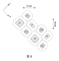
図5及び図6を参照すると、本発明のいくつかの実施例において、互いに隣接する2つの第1画素ユニット及び2つの第2画素ユニットによって重複ユニットを構成し(図6の破線枠に示す)、複数の重複ユニットは第1方向X及び第2方向Yに配列され、各重複ユニットは、それぞれ2つの第1画素ユニット及び2つの第2画素ユニットを含み、2つの第2画素ユニットは、それぞれ2つの第1画素ユニットの幾何学的中心を結ぶ線の一側に位置する。例えば、図5及び図6に示すように、複数の重複ユニットは第1方向及び第2方向にアレイ配列されて表示マトリックスを形成する。理解されるように、ノッチ付きスクリーン又はディスプレイの孔開け技術の適用に伴い、表示領域の異形エッジ領域(例えば円弧状領域)のギザギザ状も表示品質に影響する1つの要因である。異なる行におけるサブ画素は異形エッジ領域の延伸方向に段階状に形成されるため、表示パネルの画像表示時に、当該異形領域での画像のギザギザ状が深くなり、表示パネルの表示効果に影響する。従って、一実施例形態として、複数の重複ユニットは、行方向及び列方向と交差する第1方向(X方向)及び第2方向(Y方向)に配列されることができ、重複ユニットが重複して配列されることにつれて、表示領域の異形エッジに位置する複数のサブ画素のエッジの連結線と、異形エッジの接線とは重なり合い又は平行であるような傾向があり、複数のサブ画素エッジの連結線をよりスムーズにして異形エッジの形状に近くして、異形エッジでの画像のギザギザ状をさらに低減させることができ、表示パネルの表示効果の向上に寄与する。また、表示領域の異形エッジに位置するサブ画素が多種の色を含むようにし、表示パネルの異形エッジに形成されたカラーエッジをさらに低減させて、表示パネルの表示効果をさらに向上させることができる。 5 and 6, in some embodiments of the present invention, two adjacent first pixel units and two second pixel units form an overlap unit (shown in the dashed frame in FIG. 6), and the overlap units are arranged in a first direction X and a second direction Y, and each overlap unit includes two first pixel units and two second pixel units, respectively, and the two second pixel units are located on one side of a line connecting the geometric centers of the two first pixel units. For example, as shown in FIG. 5 and FIG. 6, the overlap units are arrayed in the first direction and the second direction to form a display matrix. As can be understood, with the application of the notched screen or display hole punching technology, the jagged shape of the irregular edge region (e.g., arc-shaped region) of the display area is also a factor that affects the display quality. Since the sub-pixels in different rows are formed in a stepped manner in the extension direction of the irregular edge region, when the display panel displays an image, the jagged shape of the image in the irregular region becomes deeper, which affects the display effect of the display panel. Therefore, in one embodiment, the overlapping units may be arranged in a first direction (X direction) and a second direction (Y direction) intersecting the row direction and the column direction. As the overlapping units are arranged in an overlapping manner, the connecting lines of the edges of the sub-pixels located at the irregular edge of the display area tend to overlap or be parallel to the tangents of the irregular edge. The connecting lines of the edges of the sub-pixels are made smoother and closer to the shape of the irregular edge, which further reduces the jaggedness of the image at the irregular edge, thereby contributing to improving the display effect of the display panel. In addition, the sub-pixels located at the irregular edge of the display area may include a variety of colors, which further reduces the color edge formed at the irregular edge of the display panel, thereby further improving the display effect of the display panel.
いくつかの実施例において、図5及び図6に示すように、1つの重複ユニットにおいて、いずれか1つの第2画素ユニットと、第1方向Xにそれに隣接する第1画素ユニットとにおいて、第2画素ユニット内の第2サブ画素R2の中心点と、第3サブ画素G21の中心点を結ぶ連結線の長さをL1とし、第1画素ユニット内の第2サブ画素R1の中心点と第2画素ユニット内の第3サブ画素G21の中心点を結ぶ連結線の長さをL2とすると、L1はL2と等しくない。当該第2画素ユニットと、第2方向Yにそれに隣接する他の第1画素ユニットとにおいて、第2画素ユニット内の第2サブ画素R2の中心点と、他の第1画素ユニット内の第4サブ画素G12の中心点とを結ぶ連結線の長さをL3とし、他の第1画素ユニット内の第2サブ画素R1の中心点と、第4サブ画素G12の中心点を結ぶ連結線の長さをL4とすると、L3はL4と等しくない。つまり、同一の重複ユニットにおいて、2つの隣接する画素ユニットにおいて、複数の赤色サブ画素の中心と複数の緑色サブ画素の中心を結ぶ中心連結線は長さが異なる。このようにして、各サブ画素のずれ配列を保証し、第1画素ユニットと第2画素ユニットを重複して配列して表示マトリックスを形成する場合に、同一色のサブ画素が単独して一列に配列されることをさらに回避するとともに、同一の行又は列のサブ画素の突出度合いを弱くして、表示エッジのカラーエッジ問題を改善する。 5 and 6, in one overlapping unit, in any one of the second pixel units and the first pixel unit adjacent thereto in the first direction X, if the length of the connecting line connecting the center point of the second sub-pixel R2 in the second pixel unit to the center point of the third sub-pixel G21 is L1, and the length of the connecting line connecting the center point of the second sub-pixel R1 in the first pixel unit to the center point of the third sub-pixel G21 in the second pixel unit is L2, L1 is not equal to L2. In the second pixel unit and another first pixel unit adjacent thereto in the second direction Y, if the length of the connecting line connecting the center point of the second sub-pixel R2 in the second pixel unit to the center point of the fourth sub-pixel G12 in the other first pixel unit is L3, and the length of the connecting line connecting the center point of the second sub-pixel R1 in the other first pixel unit to the center point of the fourth sub-pixel G12 is L4, L3 is not equal to L4. That is, in the same overlapping unit, the center connecting lines connecting the centers of the red sub-pixels and the centers of the green sub-pixels in two adjacent pixel units are different in length. In this way, the offset arrangement of each sub-pixel is guaranteed, and when the first pixel unit and the second pixel unit are overlapped and arranged to form a display matrix, the sub-pixels of the same color are further prevented from being arranged in a single row, and the protrusion degree of the sub-pixels in the same row or column is weakened, thereby improving the color edge problem of the display edge.
いくつかの実施例において、図6に示すように、1つの前記重複ユニットにおいて、いずれか1つの前記第2画素ユニットと、第1方向Xにそれに隣接する第1画素ユニットとにおいて、前記第2画素ユニット内の前記第2サブ画素R2、前記第3サブ画素G21、及び前記第1画素ユニット内の前記第2サブ画素R1の中心点を結ぶ連結線によって、不等辺三角形S1を構成する。そして、当該前記第2画素ユニットと、第2方向Yにそれに隣接する他の第1画素ユニットとにおいて、前記他の第1画素ユニットにおける前記第2サブ画素R1、第4サブ画素G12及び当該前記第2画素ユニット内の前記第2サブ画素R2の中心点を結ぶ連結線によって、不等辺三角形S2を構成する。つまり、同一の重複ユニットにおいて、1つの第2画素ユニット内の赤色サブ画素、行方向及び列方向において前記第2画素ユニットと隣接する第1画素ユニットにおける赤色サブ画素、及び異なる緑色サブ画素の中心を結ぶ連結線によって、それぞれ不等辺三角形を構成することができる。このようにして、第1画素ユニットと第2画素ユニットを重複して配列して表示マトリックスを形成する場合に、同一色のサブ画素が単独して一列に配列されることをさらに回避するとともに、同一の行又は列のサブ画素の突出度合いを弱くして、表示エッジのカラーエッジ問題を改善することもできる。 6, in one of the overlapping units, a scalene triangle S1 is formed by connecting lines connecting the center points of the second sub-pixel R2, the third sub-pixel G21, and the second sub-pixel R1 in the first pixel unit between any one of the second pixel units and a first pixel unit adjacent thereto in the first direction X. Then, a scalene triangle S2 is formed by connecting lines connecting the center points of the second sub-pixel R1, the fourth sub-pixel G12, and the second sub-pixel R2 in the second pixel unit between the second pixel unit and another first pixel unit adjacent thereto in the second direction Y. In other words, in the same overlapping unit, a scalene triangle can be formed by connecting lines connecting the centers of the red sub-pixel in one second pixel unit, the red sub-pixel in the first pixel unit adjacent to the second pixel unit in the row direction and the column direction, and a different green sub-pixel. In this way, when the first pixel unit and the second pixel unit are arranged in an overlapping manner to form a display matrix, it is possible to further prevent sub-pixels of the same color from being arranged alone in a column, and also to reduce the degree of protrusion of sub-pixels in the same row or column, thereby improving the color edge problem at the display edge.
いくつかの実施例において、1つの重複ユニットにおいて、任意の2つの第2サブ画素の中心を結ぶ中心連結線と、いずれか1つの第2サブ画素の中心と第3サブ画素の中心を結ぶ中心連結線とは重なり合わず、任意の2つの第2サブ画素中心を結ぶ中心連結線と、いずれか1つの第2サブ画素の中心と第4サブ画素の中心を結ぶ中心連結線とは重なり合わない。例えば、いくつかの実施例において、第2サブ画素は赤色サブ画素であり、第1サブ画素は青色サブ画素であり、第3サブ画素及び第4サブ画素は緑色サブ画素である。任意の2つの赤色サブ画素の間の連結線、例えば隣接する画素ユニットにおける第2サブ画素R1とR2の間の中心連結線は、R1/R2及びG11/G12/G21/G22のいずれか両者間の中心連結線と共線ではない。例えば、図6に示すように、第2サブ画素R1とR2の間の中心連結線LL1と、第2サブ画素R1と隣接する画素ユニットの第4サブ画素G21との間の中心連結線LL2とは重なり合わない。言い換えると、同一の重複ユニットにおいて、第1方向に隣接する第1画素ユニットと第2画素ユニットにおける2つの赤色サブ画素R1及びR2の中心連結線は、前記隣接する第1画素ユニット及び第2画素ユニットにおいて同一の画素ユニットに位置する青色サブ画素B2とG21との間を通る。同様に、第2方向に隣接する第1画素ユニット及び第2画素ユニットにおいて2つの赤色サブ画素R1とR2の中心連結線は、前記隣接する第1画素ユニット及び第2画素ユニットにおいて同一の画素ユニットに位置する青色サブ画素B1とG11の間を通る。このようにして、画素配列構造で全体として同一色の光を発するサブ画素が単独して一列に配列されることを回避するだけでなく、表示エッジのサブ画素の突出度合いをさらに弱くして、表示エッジのカラーエッジ問題を効果的に改善することができる。 In some embodiments, in one overlapping unit, the center connecting line connecting the centers of any two second subpixels does not overlap with the center connecting line connecting the center of any one of the second subpixels and the center of the third subpixel, and the center connecting line connecting the centers of any two second subpixels does not overlap with the center connecting line connecting the center of any one of the second subpixels and the center of the fourth subpixel. For example, in some embodiments, the second subpixel is a red subpixel, the first subpixel is a blue subpixel, and the third and fourth subpixels are green subpixels. The connecting line between any two red subpixels, for example, the center connecting line between the second subpixels R1 and R2 in adjacent pixel units, is not collinear with the center connecting line between either R1/R2 or G11/G12/G21/G22. For example, as shown in FIG. 6, the center connecting line LL1 between the second subpixels R1 and R2 does not overlap with the center connecting line LL2 between the second subpixel R1 and the fourth subpixel G21 of the adjacent pixel unit. In other words, in the same overlapping unit, the central connection line between the two red subpixels R1 and R2 in the first pixel unit and the second pixel unit adjacent in the first direction passes between the blue subpixels B2 and G21 located in the same pixel unit in the adjacent first pixel unit and the second pixel unit. Similarly, the central connection line between the two red subpixels R1 and R2 in the first pixel unit and the second pixel unit adjacent in the second direction passes between the blue subpixels B1 and G11 located in the same pixel unit in the adjacent first pixel unit and the second pixel unit. In this way, not only can the pixel array structure prevent subpixels emitting the same color light as a whole from being arranged in a single row, but the protrusion degree of the subpixels at the display edge can be further weakened, effectively improving the color edge problem at the display edge.
いくつかの実施例において、図6に示すように、1つの重複ユニットにおいて、各第1画素ユニットにおいて第1サブ画素中心と第3サブ画素中心を通る第1仮想接続線は互いに平行であり、各第2画素ユニットにおいて第1サブ画素の中心と第4サブ画素の中心を通る第2仮想接続線は互いに平行であり、第1仮想接続線と第2仮想接続線とは重なり合わない。具体的な実施例において、図5及び図6に示すように、同一重複ユニットにおいてB1及びG11の中心の間の連結線は互いに平行であり、即ちLL3とLL4が互いに平行であり、B2及びG22の中心の間の連結線は互いに平行であり、即ちLL5とLL6が互いに平行である。そして、同一重複ユニットにおいて、2つの同じサブ画素構造の画素ユニットにおける青色サブ画素及び緑色サブ画素の中心連結線の延長線は共線ではない。このようにして、画素配列構造で全体として同一色の光を発するサブ画素が単独して一列に配列されることを回避するとともに、表示エッジのサブ画素の突出度合いを弱くして、表示エッジのカラーエッジ問題を効果的に改善することができる。 In some embodiments, as shown in FIG. 6, in one overlapping unit, the first virtual connection lines passing through the first subpixel center and the third subpixel center in each first pixel unit are parallel to each other, and the second virtual connection lines passing through the first subpixel center and the fourth subpixel center in each second pixel unit are parallel to each other, and the first virtual connection lines and the second virtual connection lines do not overlap. In a specific embodiment, as shown in FIG. 5 and FIG. 6, in the same overlapping unit, the connecting lines between the centers of B1 and G11 are parallel to each other, i.e., LL3 and LL4 are parallel to each other, and the connecting lines between the centers of B2 and G22 are parallel to each other, i.e., LL5 and LL6 are parallel to each other. And, in the same overlapping unit, the extension lines of the central connecting lines of the blue subpixel and the green subpixel in two pixel units with the same subpixel structure are not collinear. In this way, it is possible to avoid the subpixels emitting the same color light as a whole being arranged in a row in the pixel arrangement structure, and to weaken the protruding degree of the subpixels at the display edge, thereby effectively improving the color edge problem at the display edge.
いくつかの実施例において、図6に示すように、1つの重複ユニットにおいて、1つの第1画素ユニットにおける第1サブ画素及び第2サブ画素の中心連結線と、他の第1画素ユニットにおける第1サブ画素及び第2サブ画素の中心連結線の延長線とは重なり合わず、即ちLL7とLL8が重なり合わない。1つの第2画素ユニットにおける第1サブ画素及び第2サブ画素の中心を結ぶ連結線と、他の第2画素ユニットにおける第1サブ画素及び第2サブ画素の中心を結ぶ連結線の延長線とは重なり合わない。いずれか1つの第1画素ユニットにおける第1サブ画素及び第2サブ画素の中心の間の連結線と、いずれか1つの第2画素ユニットにおける第1サブ画素及び第2サブ画素の中心の間の連結線の延長線とは重なり合わない。つまり、図5及び図6に示すように、同一重複ユニットにおいて、異なる画素ユニットにおいて、赤色サブ画素及び青色サブ画素の中心の間の連結線の延長線はいずれも共線ではない。例えば、2つの第1画素ユニットにおける赤色サブ画素R1の中心及び青色サブ画素B1の中心の間の2つの中心連結線と、2つの第2画素ユニットにおける赤色サブ画素R2の中心及び青色サブ画素B2の中心の間の2つの中心連結線とはいずれも共線ではない。理解されるように、第1サブ画素及び第2サブ画素は、第3サブ画素の中心と第4サブ画素の中心との間の連結線の両側に位置し、同一重複ユニットにおける異なる画素ユニットの赤色サブ画素及び青色サブ画素の中心の間の連結線を非共線として設定すると、同一列のサブ画素が多種の色を含み、表示エッジのカラーエッジ問題を効果的に改善する。 In some embodiments, as shown in FIG. 6, in one overlapping unit, the center connecting line of the first subpixel and the second subpixel in one first pixel unit does not overlap with the extension of the center connecting line of the first subpixel and the second subpixel in another first pixel unit, i.e., LL7 and LL8 do not overlap. The connecting line connecting the centers of the first subpixel and the second subpixel in one second pixel unit does not overlap with the extension of the connecting line connecting the centers of the first subpixel and the second subpixel in another second pixel unit. The connecting line between the centers of the first subpixel and the second subpixel in any one first pixel unit does not overlap with the extension of the connecting line between the centers of the first subpixel and the second subpixel in any one second pixel unit. That is, as shown in FIG. 5 and FIG. 6, in the same overlapping unit, the extensions of the connecting lines between the centers of the red subpixel and the blue subpixel in different pixel units are not collinear. For example, the two central connecting lines between the centers of the red subpixels R1 and the blue subpixels B1 in the two first pixel units and the two central connecting lines between the centers of the red subpixels R2 and the blue subpixels B2 in the two second pixel units are not collinear. As can be seen, the first and second subpixels are located on both sides of the connecting line between the centers of the third and fourth subpixels, and the connecting lines between the centers of the red and blue subpixels of different pixel units in the same overlapping unit are set as non-collinear, so that the subpixels in the same column contain various colors, which effectively improves the color edge problem of the display edge.
いくつかの実施例において、1つの重複ユニットにおいて、各第1画素ユニットにおいて第2サブ画素の中心と第3サブ画素の中心を通る第3仮想接続線は互いに平行であり、各第2画素ユニットにおいて第2サブ画素の中心と第4サブ画素の中心を通る第4仮想接続線は互いに平行であり、前記第3仮想接続線と前記第4仮想接続線とは重なり合わない。具体的な実施例において、図5及び図6に示すように、同一重複ユニットにおいて、2つの同じサブ画素構造の画素ユニットにおける赤色サブ画素の中心及び緑色サブ画素の中心の間の連結線の延長線は共線ではない。このようにして、画素配列構造で全体として同一色の光を発するサブ画素が単独して一列に配列されることを回避するするとともに、表示エッジのサブ画素の突出度合いを弱くして、表示エッジのカラーエッジ問題を効果的に改善することができる。 In some embodiments, in one overlapping unit, the third virtual connection lines passing through the centers of the second and third subpixels in each first pixel unit are parallel to each other, and the fourth virtual connection lines passing through the centers of the second and fourth subpixels in each second pixel unit are parallel to each other, and the third virtual connection lines and the fourth virtual connection lines do not overlap. In a specific embodiment, as shown in FIG. 5 and FIG. 6, in the same overlapping unit, the extensions of the connecting lines between the centers of the red and green subpixels in two pixel units with the same subpixel structure are not collinear. In this way, it is possible to avoid the subpixels emitting the same color light as a whole being arranged in a row in the pixel array structure, and to reduce the protrusion degree of the subpixels at the display edge, thereby effectively improving the color edge problem at the display edge.
強調すべきこととして、画面下感光デバイスの受信した光信号の光量及びコントラストはいずれも生成された物体の画像品質に影響を与え、他の画素配列構造を採用する表示パネルは、光透過可能な領域が多く、全体の光透過面積に差異がないが、特定の領域内において連続的な光透過領域の面積が小さいため、画面下感光デバイスの正常作動に必要な光透過率を満たすことができない。本発明のいくつかの実施例において、第1方向Xに隣接する第1画素ユニット及び第2画素ユニットにおいて、第1画素ユニット内の第2サブ画素R1と、当該第2画素ユニット内の第4サブ画素G21との間の距離は、当該第1画素ユニット内の第3サブ画素G11及び第4サブ画素G12と、当該第1サブ画素R1との間の距離よりも大きく、図5に示すように、例えば、L5>L6、且つ、L5>L7となる。このようにして、各重複ユニットにおいて、連続する光透過予備エリアZが形成可能となり、表示パネルの光透過率を向上させ、表示パネルの機能多様化に便利さを与える。一実施形態として、光透過予備エリアZの面積は、1つの第2サブ画素R1/R2の発光面積よりも大きい。 It should be emphasized that the light quantity and contrast of the light signal received by the under-screen photosensitive device both affect the image quality of the generated object, and the display panel adopting other pixel arrangement structures has a large light-transmitting area and no difference in the overall light-transmitting area, but the area of the continuous light-transmitting area in a specific area is small, so it cannot meet the light transmittance required for the normal operation of the under-screen photosensitive device. In some embodiments of the present invention, in the first pixel unit and the second pixel unit adjacent to each other in the first direction X, the distance between the second sub-pixel R1 in the first pixel unit and the fourth sub-pixel G21 in the second pixel unit is greater than the distance between the third sub-pixel G11 and the fourth sub-pixel G12 in the first pixel unit and the first sub-pixel R1, for example, L5>L6 and L5>L7, as shown in FIG. 5. In this way, a continuous light-transmitting spare area Z can be formed in each overlapping unit, which improves the light transmittance of the display panel and provides convenience for diversifying the functions of the display panel. In one embodiment, the area of the light-transmitting spare area Z is larger than the light-emitting area of one of the second sub-pixels R1/R2.
理解されるように、各重複ユニットは、2つの第1画素ユニット、2つの第2画素ユニット、及び隣接するサブ画素の間の隙間によって形成した光透過予備エリアZを含む。好ましくは、各重複ユニットは1つの仮想正方形内に位置し、重複ユニットがアレイ配列される場合に、複数の仮想正方形は辺を共有してアレイ配列されて表示マトリックスを形成する。このようにして、表示の均一性に寄与し、表示効果を向上させる。 As can be seen, each overlap unit includes two first pixel units, two second pixel units, and a light-transmitting spare area Z formed by the gap between adjacent sub-pixels. Preferably, each overlap unit is located within one virtual square, and when the overlap units are arrayed, multiple virtual squares are arrayed with sharing sides to form a display matrix. In this way, it contributes to the uniformity of the display and improves the display effect.
いくつかの実施例において、図7に示すように、当該画素配列構造は、4つの仮想四角形が辺を共有して配列されて形成した仮想多角形を含み、前記4つの仮想四角形は、具体的には、第1仮想四角形30、第2仮想四角形40、第3仮想四角形50及び第4仮想四角形60を含む。第1仮想四角形30は、行方向において第3仮想四角形50と第1共有辺gを共有し、列方向において第2仮想四角形40と第2共有辺hを共有する。第4仮想四角形60は、列方向において第3仮想四角形50と第3共有辺jを共有し、行方向において第2仮想四角形40と第4共有辺iを共有する。第1仮想四角形30、第2仮想四角形40、第3仮想四角形50及び第4仮想四角形60の共有辺から離れる側辺は、仮想多角形の各辺を構成する。第1サブ画素は、各仮想四角形の第1頂点に位置し、第2サブ画素は、各仮想四角形の第2頂点に位置し、第1頂点と第2頂点は交互に隔離して設けられ、緑色サブ画素は各仮想四角形内に位置する。
In some embodiments, as shown in FIG. 7, the pixel array structure includes a virtual polygon formed by arranging four virtual rectangles with their sides shared, and the four virtual rectangles specifically include a first
さらに、各前述した仮想四角形のいずれか一辺は、行方向又は列方向と平行でなく、或いは、各前述した仮想四角形の任意の二辺の長さは等しくなく、或いは、各前述した仮想四角形の任意の二辺は互いに平行でなく、或いは、各前述した仮想四角形の任意の2つの内角は等しくない。このようにして、第1仮想四角形、第2仮想四角形、第3仮想四角形及び第4仮想四角形はいずれも非規則的な四角形であり、これによってサブ画素のコンパクトな配列を満たす前提で、大きい光透過領域を形成して表示パネルの光透過率をさらに向上させ、表示パネルの機能多様化に便利さを提供することができる。 Furthermore, any one side of each of the aforementioned virtual squares is not parallel to the row direction or column direction, or any two sides of each of the aforementioned virtual squares are not equal in length, or any two sides of each of the aforementioned virtual squares are not parallel to each other, or any two interior angles of each of the aforementioned virtual squares are not equal. In this way, the first virtual square, the second virtual square, the third virtual square and the fourth virtual square are all irregular squares, which can form a large light-transmitting area on the premise of satisfying a compact arrangement of the sub-pixels, thereby further improving the light transmittance of the display panel and providing convenience for diversifying the functions of the display panel.
いくつかの実施例において、1つの画素ユニットにおいて、第1方向Xにおいて、第1サブ画素の開口部エリア、第2サブ画素開口部エリア、及び第3サブ画素の開口部エリアは互いにずれており、即ち、第2サブ画素の開口部エリアは、第1方向Xにおいて第1サブ画素の開口部及び第3サブ画素の開口部とは投影オーバーラップエリアがない。このようにして、サブ画素間の配列をよりコンパクトにすることができる。他のいくつかの実施例において、少なくとも第4サブ画素から離れる第2サブ画素の一側辺の延長線は、第3サブ画素の開口部エリアを通っていない。例えば、第2サブ画素の開口部エリアは、第1方向Xにおいて第1サブ画素の開口部エリアと部分的にオーバーラップするが、第3サブ画素とオーバーラップしていない。 In some embodiments, in one pixel unit, the aperture area of the first subpixel, the aperture area of the second subpixel, and the aperture area of the third subpixel are offset from each other in the first direction X, i.e., the aperture area of the second subpixel has no projected overlap area with the aperture of the first subpixel and the aperture of the third subpixel in the first direction X. In this way, the arrangement between the subpixels can be made more compact. In other embodiments, at least an extension line of one side of the second subpixel away from the fourth subpixel does not pass through the aperture area of the third subpixel. For example, the aperture area of the second subpixel partially overlaps the aperture area of the first subpixel in the first direction X, but does not overlap with the aperture area of the third subpixel.
いくつかの実施例において、同一の行及び/又は列に位置する緑色サブ画素の中心の連結線は非直線又は近似直線ではない。例えば、図5及び図6に示すように、同一の行及び/又は列に位置する緑色サブ画素の中心の連結線はギザギザ状を呈する。奇数の行又は列の任意の画素群における2つの緑色サブ画素と、隣接する偶数の行又は列の画素群における最も隣接する2つの緑色サブ画素との中心連結線によって、第5仮想四角形を形成し、第5仮想四角形における最小内角γ≧60°となる。このようにして、隣接する画素群における緑色サブ画素が近づきすぎないようにし、隣接する緑色サブ画素の距離が近いことによって隣接する2つの緑色サブ画素が区別されにくく、人間の目で視覚的に2つを1つとする状況をさらに回避することができる。 In some embodiments, the central connecting lines of green subpixels in the same row and/or column are not linear or approximately linear. For example, as shown in FIG. 5 and FIG. 6, the central connecting lines of green subpixels in the same row and/or column are jagged. The central connecting lines of two green subpixels in any pixel group in an odd row or column and the two most adjacent green subpixels in the pixel group in the adjacent even row or column form a fifth virtual rectangle, and the minimum interior angle γ in the fifth virtual rectangle is ≧60°. In this way, the green subpixels in the adjacent pixel groups are prevented from being too close to each other, and the situation in which the two adjacent green subpixels are difficult to distinguish due to the close distance between the adjacent green subpixels, and the human eye visually recognizes two as one, can be further avoided.
本発明の第1様態では、上述実施例の画素配列構造を含む表示パネルがさらに提供される。 The first aspect of the present invention further provides a display panel including the pixel array structure of the above embodiment.
図3乃至図7を再び参照すると、本発明の画素配列構造は下記の特徴をさらに有する。 Referring again to Figures 3 to 7, the pixel array structure of the present invention further has the following features:
本発明の画素配列構造は、前記第1画素ユニットを含む。前記第1画素ユニットは、前記第1サブ画素12、第2サブ画素14、第3サブ画素16a及び第4サブ画素16bを含む。第1サブ画素12、第2サブ画素14、第3サブ画素16a及び第4サブ画素16bは、それぞれ青色の発光サブ画素、赤色の発光サブ画素及び緑色の発光サブ画素のうちの1つであってもよい。もちろん、他のいくつかの実施例において、第1サブ画素12、第2サブ画素14、第3サブ画素16a及び第4サブ画素16bは、青色、赤色及び緑色以外の他の色の光を発するサブ画素であってもよく、例えば、第3サブ画素又は第4サブ画素は、白色又は黄色のサブ画素であってもよいが、ここで限定されない。なお、異なる色の光が異なる波長を有し、波長が短いほど光のエネルギーが高くなり、高エネルギーの光によって有機発光材料の減衰を引き起こしやすく、高エネルギーの光子を発するサブ画素はより減衰しやすくなる。青色光の波長は赤色光の波長及び緑色光の波長よりも短いため、青色光のエネルギーはより高く、青色光を発する有機発光材料は減衰しやすくなり、画素ユニットで発した光が赤っぽくなりやすく、白色光の色ずれ現象が発生してしまう。さらに、各サブ画素によって発した光は、ファブリペローマイクロキャビティ(Fabry-Perot microcavity)効果によりアノードとカソードの間で重複して反射及び再反射され、増幅及び建設的干渉が行われ、光の輝度が増加し、色ずれがさらに拡大されてしまう。好ましい一実施形態として、図3及び図4に示すように、第1サブ画素12は青色サブ画素であり、第2サブ画素14は赤色サブ画素であり、第3サブ画素16a及び第4サブ画素16bは緑色サブ画素である。ここで、青色サブ画素の発光面積は赤色サブ画素及び緑色サブ画素の発光面積よりも大きいため、異なる色の光を発する有機発光材料の減衰速度の相違による表示不良をある程度で低減させることができる。指摘されるように、いくつかの実施形態において、緑色サブ画素の発光面積は、赤色サブ画素の発光面積と等しくてもよいが、人間の目は赤色光よりも緑色光に対して敏感であるので、他のいくつかの実施形態において、緑色サブ画素の発光面積は赤色サブ画素の発光面積よりも小さくてもよいが、ここで限定されない。
The pixel array structure of the present invention includes the first pixel unit. The first pixel unit includes the
第1画素ユニットにおいて、第1サブ画素12、第2サブ画素14、第3サブ画素16a及び第4サブ画素16bのそれぞれの中心を頂点として構成された面積が重なり合わない辺を共有する三角形を有し、且つ、第1サブ画素12の中心及び第2サブ画素14の中心を前記辺を共有する三角形の共有辺の頂点とする。具体的には、図3及び図4に示すように、第1サブ画素12は、第3サブ画素16aと第4サブ画素16bとの中心連結線cの一側に位置し、第2サブ画素14は、第3サブ画素16aと第4サブ画素16bとの中心連結線cの他側に位置する。第1サブ画素12、第2サブ画素14、第3サブ画素16a及び第4サブ画素16bの中心を順次に結んで仮想四角形を形成し、第1サブ画素12、第2サブ画素14、及び第3サブ画素16aの中心を結んで第1三角形(図示なし)を構成し、第1サブ画素12、第2サブ画素14及び第4サブ画素16bの中心を結んで第2三角形を構成する。第1三角形及び第2三角形は、第1サブ画素の中心と第2サブ画素の中心を結ぶ中心連結線dを共有辺とし、即ち辺を共有する三角形となり、且つ、2つの三角形は互いに面積が重なり合わない。好ましい一実施例として、辺を共有する三角形は鋭角三角形であり、このようにして、画素構造のサブ画素の配列を均一にし、表示効果の向上に寄与する。
In the first pixel unit, the
ここで、第2サブ画素は第2長軸及び第2短軸を有し、第1画素ユニットにおいて、第2サブ画素はその長軸方向に沿う中心線が第3サブ画素及び/又は第4サブ画素の中心を通過しない。理解されるように、サブ画素の長軸方向とは、サブ画素の発光エリアの縦長延伸方向であり、サブ画素の短軸方向とは、サブ画素の発光エリアの縦長延伸方向に対向する発光エリアの幅方向である。従って、第2サブ画素の長軸方向に沿う中心線とは、サブ画素の発光エリアの縦長延伸方向に沿って第2サブ画素の中心を通過する直線である。例えば、図3に示すように、第1三角形及び第2三角形は、第1サブ画素12の中心及び第2サブ画素14の中心を結ぶ中心連結線dを共有辺とし、第2サブ画素14の長軸方向に沿う中心線とは、その中心を通過してその長軸方向に延びる直線である。第2サブ画素の長軸方向に沿う中心線は、第3サブ画素及び/又は第4サブ画素の中心を通過しないことによって、第1画素ユニット内の各サブ画素をずれ配列して、カラーエッジ問題を効果的に改善することができる。さらに、辺を共有する三角形の共有辺の頂点の、当該頂点に対向する対辺における投影は、前記対辺に位置し、且つ、当該投影は、前記第3サブ画素の中心及び/又は第4サブ画素の中心と重なり合わない。例えば、図3に示すように、第2サブ画素14の中心(中心連結線dの1つの頂点)の、その対向する対辺e(第1サブ画素の中心と第3サブ画素の中心を結ぶ中心連結線)における投影は対辺eに位置する。そして、当該投影は、第1サブ画素12の中心と第3サブ画素16aの中心と間に位置し、即ち第3サブ画素16aの中心と重なり合わない。それに対応して、第1サブ画素12の中心(中心連結線dの他の頂点)の、その対向する対辺b(第2サブ画素と第4サブ画素との中心連結線)における投影は対辺bに位置する。そして、当該投影は、第2サブ画素14の中心と第4サブ画素16bの中心との間に位置し、即ち第4サブ画素16bの中心と重なり合わない。好ましい実施形態として、当該辺を共有する三角形の共有辺の頂点の、当該頂点の対辺における投影は、前記対辺の中心点に接近するか又は位置する。このようにして、サブ画素の配列を均一に、カラーエッジ現象が現れることをさらに回避し、表示品質の向上に寄与する。
Here, the second subpixel has a second long axis and a second short axis, and in the first pixel unit, the center line of the second subpixel along its long axis direction does not pass through the center of the third subpixel and/or the fourth subpixel. As will be understood, the long axis direction of the subpixel is the vertical extension direction of the light-emitting area of the subpixel, and the short axis direction of the subpixel is the width direction of the light-emitting area opposite to the vertical extension direction of the light-emitting area of the subpixel. Therefore, the center line along the long axis direction of the second subpixel is a straight line passing through the center of the second subpixel along the vertical extension direction of the light-emitting area of the subpixel. For example, as shown in FIG. 3, the first triangle and the second triangle have a central connecting line d connecting the center of the
なお、共有辺の頂点の対辺における共有辺の頂点の投影とは、当該頂点の対辺に垂直な方向に沿って前記対辺における当該頂点の投影であり、即ち、当該頂点を通って当該頂点の対辺に垂直な垂直線と当該対辺との交差点は、前述した対辺における頂点の投影である。例えば、図3に示すように、第1三角形及び第2三角形の共有辺dの1つの頂点は第2サブ画素14の中心であり、第2サブ画素の中心を通ってその対向する対辺eに垂直な垂直線と、当該対辺eとの交差点は、前述した対向する対辺における頂点の投影である。
Note that the projection of the vertex of the shared side on the side opposite the vertex of the shared side is the projection of the vertex on the side opposite the vertex along a direction perpendicular to the side opposite the vertex. In other words, the intersection of the opposite side with a vertical line that passes through the vertex and is perpendicular to the side opposite the vertex, is the projection of the vertex on the opposite side described above. For example, as shown in FIG. 3, one vertex of the shared side d of the first triangle and the second triangle is the center of the
理解されるように、画素配列構造は表示効果を直接に決め、表示の均一性を保証するために、通常、各サブ画素を行方向及び列方向において一定のルールでできるだけ均一に配列するが、画素配列構造ではカラーエッジ及び視覚的な粒状感も生じやすい。前述した画素配列構造を採用して、サブ画素配列の均一性、緊密さ及びサブ画素間の間隔を考慮して、三者の間にバランスを取ることができ、色のにじみのリスクの低減、カラーエッジや視覚的な粒状感の改善に寄与する。例えば、表示マトリックスの形成時に、各サブ画素は前述した制限条件によってずれ配列され、同一色の光を発するサブ画素が単独に一列に配列されることを回避し、表示エッジのカラーエッジ問題を改善する。そして、ずれ配列されたサブ画素により、表示パネルの丸い角でのサブ画素をより角丸の設計に合わせ、即ち、エッジに位置するサブ画素のエッジの連結線の丸い角でのスムーズな遷移を実現し、角丸のラジアンに接するか又は一致して、丸い角でのギザギザとなる問題をさらに改善する。また、前記した画素配列構造を採用することにより、同一の画素ユニットにおける同一色のサブ画素間の距離を適切に拡大することができる。例えば、人間の目に敏感な第3サブ画素と第4サブ画素との距離を適切に拡大する一方、第1サブ画素と第2サブ画素とを互いに接近するように設定することにより、表示時に人間の目に敏感なサブ画素を区別できないため複数のサブ画素を1つとして認識することによる表示粒状感を回避できる。 As can be understood, the pixel arrangement structure directly determines the display effect and ensures the uniformity of the display, so that the sub-pixels are usually arranged as uniformly as possible in the row and column directions according to a certain rule, but the pixel arrangement structure is also prone to color edges and visual graininess. By adopting the above-mentioned pixel arrangement structure, the uniformity, closeness and spacing between the sub-pixels can be considered to balance the three, which contributes to reducing the risk of color bleeding and improving color edges and visual graininess. For example, when forming the display matrix, each sub-pixel is arranged in a shifted manner according to the above-mentioned restrictive conditions, so as to avoid sub-pixels emitting light of the same color being arranged in a single row, and to improve the color edge problem at the display edge. And the shifted sub-pixels make the sub-pixels at the round corners of the display panel more in line with the design of the round corners, i.e., to realize a smooth transition at the round corners of the connecting lines of the edges of the sub-pixels located at the edges, and to be tangent to or coincident with the radians of the round corners, thereby further improving the problem of jagged edges at the round corners. In addition, by adopting the pixel array structure described above, the distance between subpixels of the same color in the same pixel unit can be appropriately increased. For example, by appropriately increasing the distance between the third and fourth subpixels, which are sensitive to the human eye, while setting the first and second subpixels to be close to each other, it is possible to avoid the graininess of the display caused by multiple subpixels being recognized as one because the subpixels sensitive to the human eye cannot be distinguished during display.
強調すべきこととして、画面下感光デバイスの受信した光信号の光量及びコントラストはいずれも生成された画像品質に影響を与え、他の画素配列構造を採用する表示パネルは、光透過可能な領域が多く、全体の光透過面積に差異がないが、特定の領域内において連続的な光透過領域の面積が小さいため、画面下感光デバイスの正常作動に必要な光透過率を満たすことができない。前述した画素配列の制限条件を採用して、1つの画素ユニットにおいてずれ配列して光透過予備エリアZを形成することもでき、例えば画面下撮像の表示ディスプレイの作製の実現に寄与する。例えば、図5及び図6に示すように、第1画素ユニット及び第2画素ユニットには、第2サブ画素14の外側に設けられた空白エリアがさらに含まれ、当該空白エリアは、前述した光透過予備エリアZであり、当該領域は、外部光線が貫通して画面下まで達する感光デバイスとして予め設けられてもよい。具体的な1つの実施例において、前記光透過予備エリアZは、第1方向におけるサイズ範囲が10μm~90μmであり、第2方向におけるサイズ範囲が20μm~90μmである。
It should be emphasized that the light quantity and contrast of the light signal received by the under-screen photosensitive device both affect the generated image quality, and the display panel adopting other pixel arrangement structures has many light-transmittable areas and no difference in the overall light-transmitting area, but the area of the continuous light-transmitting area in a specific area is small, so it cannot meet the light transmittance required for the normal operation of the under-screen photosensitive device. The above-mentioned pixel arrangement restriction conditions can also be adopted to form a light-transmitting spare area Z by staggering in one pixel unit, which contributes to the realization of, for example, the realization of the production of a display for under-screen imaging. For example, as shown in FIG. 5 and FIG. 6, the first pixel unit and the second pixel unit further include a blank area provided outside the
いくつかの実施例において、当該画素配列構造は複数の第2画素ユニットをさらに含む。第1画素ユニット及び第2画素ユニットは互いに隣接し、且つ、複数の第1画素ユニットと複数の第2画素ユニットは第1方向及び第2方向において交互に配列される。例えば、図5に示すように、第1方向はX方向であり、第2方向はY方向である。第1方向において、第1画素ユニット及び第2画素ユニットは交互に配列され、第2方向において、第1画素ユニット及び第2画素ユニットは交互に配列される。つまり、第1方向及び第2方向において、任意の2つの隣接する第1画素ユニットは1つの第2画素ユニットによって隔離され、任意の2つの隣接する第2画素ユニットは1つの第1画素ユニットによって隔離される。理解されるように、他のいくつかの実施例において、当該第1方向及び第2方向は、他の行方向及び列方向と交差する方向であってもよいが、ここで限定されない。例えば、図6に示すように、第1方向と行方向との夾角が45°であり、第2方向は第1方向に垂直であり、列方向との夾角が45°である。 In some embodiments, the pixel array structure further includes a plurality of second pixel units. The first pixel unit and the second pixel unit are adjacent to each other, and the plurality of first pixel units and the plurality of second pixel units are alternately arranged in the first direction and the second direction. For example, as shown in FIG. 5, the first direction is the X direction, and the second direction is the Y direction. In the first direction, the first pixel units and the second pixel units are alternately arranged, and in the second direction, the first pixel units and the second pixel units are alternately arranged. That is, in the first direction and the second direction, any two adjacent first pixel units are separated by one second pixel unit, and any two adjacent second pixel units are separated by one first pixel unit. It is understood that in some other embodiments, the first direction and the second direction may be directions intersecting with other row directions and column directions, but are not limited thereto. For example, as shown in FIG. 6, the included angle between the first direction and the row direction is 45°, and the second direction is perpendicular to the first direction and has an included angle of 45° with the column direction.
いくつかの実施例において、第2画素ユニットにおける各サブ画素構造は、所定角度だけ回転した後に、前記第1画素ユニットにおける各サブ画素構造と鏡像対称となる。つまり、第1画素ユニットにおけるサブ画素及び第2画素ユニットにおける同一色のサブ画素の形状、サイズ(発光面積)は同じであり、第2画素ユニットにおけるサブ画素が時計回り又は反時計回りに所定角度だけ回転した後のサブ画素構造は、第1画素ユニットにおける対応するサブ画素の構造と鏡像対称である。ここで、前記所定角度は0°よりも大きく360°未満であり、例えば、図4に示す第2画素ユニットにおける各サブ画素配列構造は90°だけ回転した後に、第1方向において図3に示す第1画素ユニットにおける各サブ画素配列構造と鏡像対称となる。このようにして、行方向又は列方向において同一色の光を発するサブ画素が単独して一列に配列されることを回避するだけではなく、同一の行又は列に位置するサブ画素の突出度合いを弱くして、表示エッジのカラーエッジ問題をさらに改善する。そして、色ずれを効果的に改善することもでき、例えば、第3サブ画素及び第4サブ画素を人間の目に敏感な色のサブ画素、例えば緑色サブ画素としてもよく、各緑色サブ画素はいずれも赤色サブ画素及び青色サブ画素によって囲まれてもよく、これによって色のにじみがより均一になり、色ずれを改善する。また、第2画素ユニットにおける各サブ画素構造は所定角度だけ回転した後に第1画素ユニットにおける各サブ画素構造と鏡像対称となり、隣接する画素ユニットの間に面積が大きい光透過予備エリアZ(図6参照)をできるだけ形成し、画面下感光デバイスの光収集面積の向上に寄与する。理解されるように、別のいくつかの実施例において、第1画素ユニット及び第2画素ユニットのサブ画素構造は同一であってもよいが、ここで限定されない。つまり、画素配列構造における最小重複ユニットは1つの画素ユニットである。 In some embodiments, each subpixel structure in the second pixel unit is mirror-symmetric to each subpixel structure in the first pixel unit after being rotated by a predetermined angle. That is, the shape and size (light-emitting area) of the subpixel in the first pixel unit and the subpixel of the same color in the second pixel unit are the same, and the subpixel structure after the subpixel in the second pixel unit is rotated by a predetermined angle clockwise or counterclockwise is mirror-symmetric to the structure of the corresponding subpixel in the first pixel unit. Here, the predetermined angle is greater than 0° and less than 360°, for example, each subpixel arrangement structure in the second pixel unit shown in FIG. 4 is mirror-symmetric to each subpixel arrangement structure in the first pixel unit shown in FIG. 3 in the first direction after being rotated by 90°. In this way, not only is it possible to avoid that subpixels emitting light of the same color are arranged in a single row or column direction, but also to weaken the protruding degree of subpixels located in the same row or column, thereby further improving the color edge problem of the display edge. And the color shift can be effectively improved. For example, the third and fourth sub-pixels can be sub-pixels of a color that is sensitive to the human eye, such as green sub-pixels, and each green sub-pixel can be surrounded by a red sub-pixel and a blue sub-pixel, so that the color bleeding is more uniform and the color shift can be improved. In addition, each sub-pixel structure in the second pixel unit is mirror-symmetrical to each sub-pixel structure in the first pixel unit after rotating by a certain angle, so as to form a large light-transmitting spare area Z (see FIG. 6) between adjacent pixel units as much as possible, which contributes to improving the light collection area of the under-screen photosensitive device. It can be understood that in some other embodiments, the sub-pixel structures of the first pixel unit and the second pixel unit can be the same, but are not limited thereto. That is, the minimum overlap unit in the pixel array structure is one pixel unit.
さらに、いくつかの実施例において、第1方向において、第1画素ユニットと隣接する第2画素ユニットとは第1画素群を構成する。第2方向において、第1画素ユニットと隣接する第2画素ユニットとは第2画素群を構成する。言い換えると、第1方向において、1つの第1画素ユニットと隣接する1つの第2画素ユニットとは第1画素群を構成し、第2方向において、1つの第1画素ユニットと隣接する1つの第2画素ユニットとは第2画素群を構成する。具体的には、図5、図6及び図7に示す実施例において、画素ユニットを単位として、2つの第1画素ユニット及び2つの第2画素ユニットは1つの重複ユニットを構成し、2つの第2画素ユニットはそれぞれ2つの第1画素ユニットの幾何学的中心の連結線の一側に位置する。画素群を単位として、2つの隣接する第1画素群又は2つの隣接する第2画素群は1つの重複ユニットを構成し、複数の重複ユニットは第1方向及び第2方向に配列される。ここで、第1画素群において、第3サブ画素の中心又は第4サブ画素の中心は第1画素群における2つの第2サブ画素の中心連結線の外側に位置し、及び/又は第2画素群において第3サブ画素の中心又は第4サブ画素の中心は、第2画素群における2つの第2サブ画素の中心連結線の外側に位置する。このようにして、サブ画素の配列が均一であるようにできるだけ保証する前提で、サブ画素をずれ配列し、重複ユニットが重複して配列されて表示マトリックスを形成する時に、同一色のサブ画素が単独に一列に配列されることをさらに回避するとともに、同一の行又は列のサブ画素の突出度合いを弱くして、表示エッジのカラーエッジ問題を改善することができる。なお、解像度を向上させるために、サブピクセルレンダリング技術を利用するが、フルカラー表示を実現するために隣のサブ画素から表示できない色を借用する必要がある。したがって、サブ画素配列が均一であるとは、各サブ画素間の距離が合理的な範囲にあり、画素配列構造における一部の領域のサブ画素の距離が小さすぎて緊密であり、一部の領域のサブ画素の距離が大きすぎて緩くなり、表示効果が低いことを回避するという意味である。 Furthermore, in some embodiments, in the first direction, the first pixel unit and the adjacent second pixel unit form a first pixel group. In the second direction, the first pixel unit and the adjacent second pixel unit form a second pixel group. In other words, in the first direction, one first pixel unit and one adjacent second pixel unit form a first pixel group, and in the second direction, one first pixel unit and one adjacent second pixel unit form a second pixel group. Specifically, in the embodiments shown in FIG. 5, FIG. 6 and FIG. 7, two first pixel units and two second pixel units form one overlapping unit with respect to a pixel unit, and two second pixel units are respectively located on one side of a connecting line of the geometric center of two first pixel units. With respect to a pixel group, two adjacent first pixel groups or two adjacent second pixel groups form one overlapping unit, and a plurality of overlapping units are arranged in the first direction and the second direction. Here, in the first pixel group, the center of the third subpixel or the center of the fourth subpixel is located outside the central connecting line of the two second subpixels in the first pixel group, and/or the center of the third subpixel or the center of the fourth subpixel in the second pixel group is located outside the central connecting line of the two second subpixels in the second pixel group. In this way, under the premise of ensuring that the arrangement of the subpixels is uniform as much as possible, when the subpixels are arranged in a staggered manner and the overlapping units are arranged in an overlapping manner to form a display matrix, it is possible to further avoid that the subpixels of the same color are arranged in a single row, and the protruding degree of the subpixels in the same row or column is weakened, thereby improving the color edge problem of the display edge. In addition, in order to improve the resolution, the subpixel rendering technology is used, but in order to realize full-color display, it is necessary to borrow colors that cannot be displayed from adjacent subpixels. Therefore, the uniform subpixel arrangement means that the distance between each subpixel is within a reasonable range, and the distance between the subpixels in some areas in the pixel arrangement structure is too small and close, and the distance between the subpixels in some areas is too large and loose, which prevents the display effect from being poor.
理解されるように、ノッチ付きスクリーン又はディスプレイの孔開け技術の適用に伴い、表示領域の異形エッジ領域(例えば円弧状領域)のギザギザ状も表示品質に影響する1つの要因である。本発明の発明者らは研究した結果、異なる行におけるサブ画素は異形エッジ領域の延伸方向に段階状に形成されるため、表示パネルの画像表示時に、当該異形領域での画像のギザギザ状が深くなり、表示パネルの表示効果に影響することを発見した。従って、一実施形態として、複数の重複ユニットは、行方向及び列方向と斜めに交差する第1方向及び第2方向において配列されることができ、重複ユニットが重複して配列されることにより、表示領域の異形エッジに位置する複数のサブ画素のエッジの連結線と、異形エッジの接線とは重なり合い又は平行であるように傾向があることによって、複数のサブ画素のエッジの連結線をよりスムーズにして異形エッジの形状に近くして、異形エッジにおける画像のギザギザ状をさらに低減させることができ、表示パネルの表示効果の向上に寄与する。また、表示領域の異形エッジに位置するサブ画素が多種の色を含むようにし、表示パネルの異形エッジに形成されたカラーエッジをさらに低減させて、表示パネルの表示効果をさらに向上させることができる。好ましくは、第1方向と第2方向とは互いに垂直であり、第1方向と行方向との夾角は45°であることが好ましい。 As can be understood, with the application of the hole-drilling technology of the notched screen or display, the jaggedness of the irregular edge region (e.g., arc-shaped region) of the display area is also a factor that affects the display quality. As a result of research, the inventors of the present invention have found that since the sub-pixels in different rows are formed in a stepped manner in the extension direction of the irregular edge region, when an image is displayed on the display panel, the jaggedness of the image in the irregular region becomes deeper, which affects the display effect of the display panel. Therefore, in one embodiment, the multiple overlapping units can be arranged in a first direction and a second direction that diagonally cross the row direction and the column direction, and the overlapping units are arranged in an overlapping manner, so that the connecting lines of the edges of the multiple sub-pixels located at the irregular edge of the display area tend to overlap or be parallel to the tangent lines of the irregular edge, making the connecting lines of the edges of the multiple sub-pixels smoother and closer to the shape of the irregular edge, thereby further reducing the jaggedness of the image at the irregular edge, which contributes to improving the display effect of the display panel. In addition, the sub-pixels located at the irregular edge of the display area can include a variety of colors, further reducing the color edge formed at the irregular edge of the display panel, thereby further improving the display effect of the display panel. Preferably, the first direction and the second direction are perpendicular to each other, and the included angle between the first direction and the row direction is preferably 45°.
いくつかの実施例において、第3サブ画素16aの中心又は第4サブ画素16bの中心は、第1画素ユニットにおける第2サブ画素14の中心と、当該第1画素ユニットに隣接する第2画素ユニットにおける第2サブ画素14の中心を結ぶ連結線の外側に位置する。言い換えると、一方の画素ユニットにおける第3サブ画素16aの中心又は第4サブ画素16bの中心は、その位置する画素ユニットにおける第2サブ画素14の中心と、隣接する他方の画素ユニットにおける第2サブ画素14の中心を結ぶ連結線の外側に位置する。例えば、具体的には、いくつかの実施例において、図5及び図6に示すように、第1画素ユニットにおける第2サブ画素R1の中心と、第1画素ユニットに隣接する第2画素ユニットにおける第2サブ画素R2の中心を結ぶ連結線の延長線は、第1画素ユニットにおける第3サブ画素G11の中心及び第4サブ画素G12の中心とはずれており、且つ、第3サブ画素G11の中心及び第4サブ画素G12の中心は前述した連結線の延長線の両側に位置する。なお、サブ画素の中心が中心連結線の外側に位置することとは、サブ画素の中心と中心を結ぶ連結線及びその延長線とはずれており、例えば、サブ画素の中心は中心連結線及びその延長線の一側に位置する。
In some embodiments, the center of the
好ましい実施形態として、第1サブ画素及び第2サブ画素は、それぞれ青色サブ画素及び赤色サブ画素であってもよく、第3サブ画素及び第4サブ画素は緑色サブ画素であってもよく、青色及び赤色サブ画素よりも、緑色サブ画素は発光面積が小さい。同一の画素ユニットにおいて、第1サブ画素の中心と第2サブ画素の中心を結ぶ連結線dは、第3サブ画素の中心と第4サブ画素の中心を結ぶ連結線cとは長さが等しくない。容易に理解されるように、通常、異なる色の光を発するサブ画素の発光面積は大きさが異なり、例えば、青色サブ画素の発光面積は、赤色サブ画素及び緑色サブ画素の発光面積の大きさよりも大きい。中心連結線dの長さを中心連結線cの長さと等しくないように設計することによって、第1サブ画素と第2サブ画素との間の間隔、及び第3サブ画素と第4サブ画素との間隔が所定条件を満たすことを保証することができ、これにより、各サブ画素をできるだけ緊密に配列するとともの、敏感な色のサブ画素の分布均一性を改善し、視覚的な解像度を向上させ、表示品質を向上させるができる。 In a preferred embodiment, the first and second subpixels may be blue and red subpixels, respectively, and the third and fourth subpixels may be green subpixels, with the green subpixel having a smaller light-emitting area than the blue and red subpixels. In the same pixel unit, the connecting line d connecting the center of the first subpixel to the center of the second subpixel is not equal in length to the connecting line c connecting the center of the third subpixel to the center of the fourth subpixel. As can be easily understood, the light-emitting areas of subpixels emitting different colors of light are usually different in size, for example, the light-emitting area of the blue subpixel is larger than the light-emitting area of the red subpixel and the light-emitting area of the green subpixel. By designing the length of the central connecting line d to be unequal to the length of the central connecting line c, it is possible to ensure that the interval between the first and second subpixels and the interval between the third and fourth subpixels meet a predetermined condition, thereby arranging each subpixel as closely as possible, improving the distribution uniformity of the subpixels of sensitive colors, improving the visual resolution, and improving the display quality.
図3及び図4に示すように、1つの画素ユニットにおいて第1サブ画素の中心と第3サブ画素の中心を結ぶ連結線eの長さは、同一の画素ユニットにおいて第1サブ画素の中心と第4サブ画素の中心を結ぶ連結線aの長さと等しくない。具体的には、一実施例において、第1サブ画素は青色サブ画素であり、第2サブ画素は赤色サブ画素であり、第3サブ画素及び第4サブ画素は緑色サブ画素である。同一の画素ユニットにおいて、青色サブ画素と、異なる緑色サブ画素の中心連結線の長さは異なる。他のいくつかの実施例において、1つの画素ユニットにおいて、第3サブ画素の中心及び第4サブ画素の中心のそれぞれは、第2サブ画素の中心までの距離が等しくない。このようにして、一方では、隣接するサブ画素が近づきすぎないようにし、隣接するサブ画素の距離が近いことによって隣接する2つのサブ画素が区別されにくく、人間の目で視覚的に2つを1つとする状況をさらに回避する。他方では、第1サブ画素及び第2サブ画素と、第3サブ画素及び第4サブ画素の中心連結線の長さが異なるように設定することによって、サブ画素のずれ配列を深化させ、第1画素ユニットと第2画素ユニットが重複して配列されて表示マトリックスを形成する場合に、同一色のサブ画素が単独して一列に配列されることをさらに回避するとともに、同一の行又は列のサブ画素の突出度合いを弱くして、表示エッジのカラーエッジ問題を改善する。 3 and 4, the length of the connecting line e connecting the center of the first subpixel to the center of the third subpixel in one pixel unit is not equal to the length of the connecting line a connecting the center of the first subpixel to the center of the fourth subpixel in the same pixel unit. Specifically, in one embodiment, the first subpixel is a blue subpixel, the second subpixel is a red subpixel, and the third and fourth subpixels are green subpixels. In the same pixel unit, the center connecting lines of the blue subpixel and the different green subpixels are different in length. In some other embodiments, in one pixel unit, the center of the third subpixel and the center of the fourth subpixel are not equal in distance to the center of the second subpixel. In this way, on the one hand, adjacent subpixels are prevented from being too close to each other, and the situation in which the two adjacent subpixels are difficult to distinguish due to the close distance between the adjacent subpixels, and the human eye visually sees two as one, is further avoided. On the other hand, by setting the central connecting lines of the first and second subpixels and the third and fourth subpixels to have different lengths, the offset arrangement of the subpixels is deepened, and when the first pixel unit and the second pixel unit are arranged in an overlapping arrangement to form a display matrix, subpixels of the same color are further prevented from being arranged alone in a row, and the degree of protrusion of subpixels in the same row or column is weakened, thereby improving the color edge problem at the display edge.
さらに、第3サブ画素の中心及び第4サブ画素の中心のそれぞれは、第1サブ画素の中心までの距離の比が(3~2):(2~1)である。第3サブ画素の中心及び第4サブ画素の中心のそれぞれは、前記第2サブ画素の中心までの距離の比も(3~2):(2~1)である。理解されるように、表示品質の影響因子は、カラーエッジ、粒状感の他に、重要な要因として解像度、均一性があるので、第3サブ画素及び第4サブ画素の中心から第1サブ画素及び第2サブ画素の中心までの距離の比をさらに限定することにより、サブ画素の配列は均一性、コンパクト性、位置ずれ度合いの間に良好なバランスを取って、表示品質を総合的に向上させる。 Furthermore, the ratio of the distance between the center of the third subpixel and the center of the fourth subpixel to the center of the first subpixel is (3 to 2):(2 to 1). The ratio of the distance between the center of the third subpixel and the center of the fourth subpixel to the center of the second subpixel is also (3 to 2):(2 to 1). As can be seen, in addition to color edges and graininess, important factors affecting display quality include resolution and uniformity. Therefore, by further limiting the ratio of the distance between the centers of the third and fourth subpixels and the centers of the first and second subpixels, the subpixel arrangement achieves a good balance between uniformity, compactness, and the degree of misalignment, thereby improving the overall display quality.
なお、サブ画素の中心は、サブ画素の図形の幾何学的中心であってもよいし、サブ画素の発光色の中心であってもよいが、ここで限定されない。 The center of the subpixel may be the geometric center of the shape of the subpixel or the center of the emission color of the subpixel, but is not limited thereto.
さらに、同一の画素ユニットにおいて、第1方向及び第2方向において、隣接する2つのサブ画素間の最小距離をpとすると、第1方向及び第2方向において、隣接する2つの画素ユニットにおいて最も隣接する異なる色のサブ画素間の最小距離もpである。ここで、10μm<p<30μmである。このようにして、一方では、サブ画素の配列をより均一して、表示品質の向上に寄与し、他方では、隣接するサブ画素間の発光クロストーク又は干渉によるギザギザ状を効果的に回避することができる。なお、本発明の実施例で提供される表示パネルは、有機発光表示パネルであってもよく、サブ画素は、少なくともアノード、カソード、及びアノードとカソードの間に位置する発光層を含み、駆動回路によってアノードとカソードの間に電圧を印加し、キャリアの遷移を励起し、発光層に作用して光線を射出する。隣接するサブ画素間にクロストーク又は干渉が生じることを回避するために、表示パネルは画素定義層をさらに含んでもよく、画素定義層は複数の画素開口部を定義し、サブ画素の発光層は画素開口部内に設けられている。従って、画素開口部の面積は、サブ画素の発光面積である。しかし、蒸着技術に限られるため、発光材料が完全に画素開口部内に蒸着されるように保証するために、通常、蒸着マージンを残すために、マスク板の開口部の面積は画素開口部の面積よりも大きくされる。例えば、図3に示すように、サブ画素の内側辺は画素辺と称され、即ち画素定義層(PDL層)の画素開口部の境界であり、外側辺はサブ画素の仮想辺と称され、前記仮想辺とはマスク(マスク板)の蒸着開口部の境界である。故に、本発明の実施例において、サブ画素間の間隔とは、2つのサブ画素の画素辺間の距離である。具体的には、図3及び図4に示す実施例において、隣接する2つのサブ画素間は、隣接して平行である2つの画素辺を有すると、隣接する2つのサブ画素間の最小距離は、当該互いに隣接して平行である2つの画素辺間の垂直距離である。 Furthermore, in the same pixel unit, if the minimum distance between two adjacent subpixels in the first and second directions is p, the minimum distance between the most adjacent subpixels of different colors in two adjacent pixel units in the first and second directions is also p. Here, 10 μm<p<30 μm. In this way, on the one hand, the arrangement of the subpixels can be made more uniform, contributing to improving the display quality, and on the other hand, the jagged shape caused by light emission crosstalk or interference between adjacent subpixels can be effectively avoided. It should be noted that the display panel provided in the embodiment of the present invention may be an organic light emitting display panel, and the subpixel includes at least an anode, a cathode, and a light emitting layer located between the anode and the cathode, and a voltage is applied between the anode and the cathode by a driving circuit to excite the transition of carriers and act on the light emitting layer to emit light. In order to avoid crosstalk or interference between adjacent subpixels, the display panel may further include a pixel definition layer, and the pixel definition layer defines a plurality of pixel openings, and the light emitting layer of the subpixel is provided in the pixel opening. Therefore, the area of the pixel opening is the light-emitting area of the subpixel. However, due to the limitations of deposition technology, in order to ensure that the light-emitting material is completely deposited in the pixel opening, the area of the opening of the mask plate is usually made larger than the area of the pixel opening to leave a deposition margin. For example, as shown in FIG. 3, the inner side of the subpixel is called the pixel side, that is, the boundary of the pixel opening of the pixel definition layer (PDL layer), and the outer side is called the virtual side of the subpixel, and the virtual side is the boundary of the deposition opening of the mask (mask plate). Therefore, in the embodiment of the present invention, the spacing between the subpixels is the distance between the pixel sides of the two subpixels. Specifically, in the embodiment shown in FIG. 3 and FIG. 4, if two adjacent subpixels have two pixel sides that are adjacent and parallel to each other, the minimum distance between the two adjacent subpixels is the vertical distance between the two pixel sides that are adjacent and parallel to each other.
さらに、第1画素ユニットにおける第2サブ画素と、第1方向において隣接して配列された第2画素ユニットの第3サブ画素との間の最小距離をqとすると、p<q<3pとなる。このようにして、十分な大きさの光透過予備エリアZを保証し、画面下感光デバイスの正常作動に必要な光量を満たすことができる。 Furthermore, if the minimum distance between the second sub-pixel in the first pixel unit and the third sub-pixel in the second pixel unit arranged adjacently in the first direction is q, then p<q<3p. In this way, a sufficiently large light-transmitting spare area Z can be guaranteed to meet the amount of light required for the normal operation of the under-screen photosensitive device.
図5、図6及び図7に示すように、好ましい実施形態として、第1サブ画素、第2サブ画素、第3サブ画素及び第4サブ画素は、いずれも矩形又は矩形に近い形状であってもよく、第1サブ画素、第2サブ画素、第3サブ画素及び第4サブ画素の長軸方向(延伸方向)は行方向及び列方向と交差する。このように、一方では、他のサブ画素の形状に比べると、サブ画素間の配列は緊密にするとともに、同一色のサブ画素が独立して一行をなし、カラーエッジ現象を効果的に改善することができる。他方では、表示パネルの異形エッジに位置するサブ画素をより角丸の設計に合わせ、即ち、サブ画素の傾斜が角丸のラジアンに接するか又は一致するようにし、各サブ画素のエッジの丸い角でのスムーズな遷移を実現して、丸い角でのギザギザとなる問題を改善する。好ましくは、第1サブ画素、第2サブ画素、第3サブ画素及び第4サブ画素の延伸方向は、第1方向に平行であり、行方向又は列方向との夾角が30°~60°である。このように、さらにサブ画素の傾斜が角丸のラジアンに接するか又は一致するようにし、各サブ画素エッジの丸い角でのスムーズな遷移を実現して、さらに丸い角でのギザギザとなる問題を改善することができる。強調すべきこととして、人間の目が水平又は垂直方向における画面品質に対して敏感である一方、水平方向との夾角が45°である方向における画面品質に対してあまり敏感ではないため、好ましい実施形態として、図7に示すように、第1方向と行方向との夾角は45°であることにより、全体的な表示品質を向上させることができる。特に指摘されるように、マスク板に受けられた力は、通常、行方向又は列方向に伝達され、例えば、引張力Fは行方向に伝達され、対応するサブ画素が行方向又は列方向に対して傾斜して設けられたマスク板の開口部は、受けられた力を行方向及び列方向に分解することができ、それによってFMMの引張力Fの集中による開口部の変形を回避し、マスク板の作製難しさ及び引張難しさを低減する。そして、マスク板の開口部が傾斜して設けられるため、同じ長さ及び幅のマスク板において、より多くの開口部を設けることができ、マスクの作製コストを低減させる。 5, 6 and 7, in a preferred embodiment, the first, second, third and fourth subpixels may be rectangular or nearly rectangular, and the long axis directions (extension directions) of the first, second, third and fourth subpixels cross the row and column directions. In this way, on the one hand, compared with other subpixel shapes, the arrangement between the subpixels is closer, and the subpixels of the same color are arranged in a row independently, which can effectively improve the color edge phenomenon. On the other hand, the subpixels located on the irregular edge of the display panel are more in line with the round corner design, that is, the slope of the subpixel is tangent to or coincides with the radian of the round corner, so as to realize a smooth transition at the round corner of the edge of each subpixel and improve the problem of jagged edges at the round corner. Preferably, the extension direction of the first, second, third and fourth subpixels is parallel to the first direction and has an included angle of 30° to 60° with the row or column direction. In this way, the inclination of the subpixel can be made to be tangent to or coincident with the radian of the rounded corner, so that the smooth transition at the rounded corner of each subpixel edge can be realized, and the problem of jagged edges at the rounded corner can be further improved. It should be emphasized that the human eye is sensitive to the screen quality in the horizontal or vertical direction, but is not very sensitive to the screen quality in the direction with an included angle of 45° with the horizontal direction, so that the included angle between the first direction and the row direction is 45° as shown in FIG. 7 as a preferred embodiment, so that the overall display quality can be improved. As particularly pointed out, the force received by the mask plate is usually transmitted in the row direction or column direction, for example, the tensile force F is transmitted in the row direction, and the opening of the mask plate with the corresponding subpixel inclined to the row direction or column direction can resolve the received force in the row direction and the column direction, thereby avoiding the deformation of the opening due to the concentration of the tensile force F of the FMM, and reducing the difficulty of manufacturing and tensile the mask plate. And because the openings in the mask plate are angled, more openings can be provided in a mask plate of the same length and width, reducing the cost of manufacturing the mask.
もちろん、第1サブ画素、第2サブ画素、第3サブ画素及び第4サブ画素は他の形状であってもよく、ここで限定されない。例えば、第1サブ画素は正方形であり、第2サブ画素、第3サブ画素及び第4サブ画素は長方形であるようにしてもよい。 Of course, the first, second, third and fourth sub-pixels may have other shapes and are not limited here. For example, the first sub-pixel may be a square, and the second, third and fourth sub-pixels may be rectangular.
本発明のいくつかの実施例において、辺を共有する三角形の共有辺において、少なくとも1つの頂点の当該頂点の対辺における投影は、全体として当該対辺の対応する2つのサブ画素の輪郭と当該対辺との交差点の間に位置する。言い換えると、辺を共有する三角形の共有辺の頂点を通って当該頂点の対辺に垂直である直線と、当該頂点の対辺との交差点は、当該頂点の対辺の対応する2つのサブ画素の輪郭と当該頂点の対辺との交差点の間に位置する。さらに、1つの画素ユニットにおいて、第2サブ画素の長軸方向に沿う側辺の延長線又は当該側辺の接線は、第3サブ画素及び/又は第4サブ画素が全体として交差しない。例えば、辺を共有する三角形の共有辺の頂点に対応するサブ画素の、当該頂点の対辺における投影は全体として当該頂点の対辺の対応する2つのサブ画素の輪郭と当該頂点の対辺との交差点の間に位置する。このようにして、第2サブ画素の長軸方向に沿う側辺の延長線又は当該側辺の接線と、第3サブ画素及び/又は第4サブ画素とが全体として交差しなくてもよい。具体的には、いくつかの実施例において、図3及び図4に示すように、共有辺の2つの頂点はそれぞれ第1サブ画素の中心及び第2サブ画素の中心である。サブ画素の配列をより均一にするとともに作製難しさを低減するために、互いに隣接する2つのサブ画素は、互いに対向し且つ平行である2つの画素辺を有する。例えば、第1サブ画素及び第3サブ画素は、互いに対向し且つ平行である2つの画素辺を有し、前記2つの画素辺は、第1サブ画素及び第3サブ画素の輪郭の境界である。対辺eに向く第2サブ画素の投影の全体は、対辺eと、第1サブ画素の輪郭及び第2サブ画素の輪郭との交差点の間に位置し、即ち対辺eに向く第2サブ画素の投影は、対辺eと、第1サブ画素及び第2サブ画素の互いに対向し且つ平行である2つの画素辺との交差点の間に位置する。理解されるように、図3に示す実施例において、対辺bに向く第1サブ画素の投影の全体は、対辺bと、第2サブ画素及び第3サブ画素の中心連結線との間に位置しないが、当該技術思想への理解を影響しない。他のいくつかの実施例において、対辺bに向く第1サブ画素の投影の全体は、対辺bと、第2サブ画素及び第3サブ画素の互いに対向し且つ平行である2つの画素辺との交差点の間に位置してもよい。このようにして、一方ではサブ画素の配列をより均一にし、他方では、サブ画素をずれて配列してカラーエッジ現象をさらに低減させる。 In some embodiments of the present invention, in a shared side of a triangle that shares a side, the projection of at least one vertex on the opposite side of the vertex is located as a whole between the intersection point of the opposite side and the contours of the two subpixels corresponding to the opposite side of the vertex. In other words, the intersection point of a straight line that passes through a vertex of a shared side of a triangle that shares a side and is perpendicular to the opposite side of the vertex and the opposite side of the vertex is located as a whole between the intersection point of the contours of the two subpixels corresponding to the opposite side of the vertex and the opposite side of the vertex. Furthermore, in one pixel unit, the extension line of the side along the long axis direction of the second subpixel or the tangent line of the side does not cross the third subpixel and/or the fourth subpixel as a whole. For example, the projection of the vertex of a subpixel corresponding to a shared side of a triangle that shares a side on the opposite side of the vertex is located as a whole between the intersection point of the contours of the two subpixels corresponding to the opposite side of the vertex and the opposite side of the vertex. In this way, the extension line of the side along the long axis direction of the second subpixel or the tangent line of the side may not intersect with the third subpixel and/or the fourth subpixel as a whole. Specifically, in some embodiments, as shown in FIG. 3 and FIG. 4, the two vertices of the shared side are the centers of the first subpixel and the second subpixel, respectively. In order to make the arrangement of the subpixels more uniform and reduce the difficulty of fabrication, two adjacent subpixels have two pixel sides that are opposite and parallel to each other. For example, the first subpixel and the third subpixel have two pixel sides that are opposite and parallel to each other, and the two pixel sides are the boundaries of the contours of the first subpixel and the third subpixel. The entire projection of the second subpixel toward the opposite side e is located between the intersection point of the opposite side e with the contour of the first subpixel and the contour of the second subpixel, i.e., the projection of the second subpixel toward the opposite side e is located between the intersection point of the opposite side e with the two pixel sides of the first subpixel and the second subpixel that are opposite and parallel to each other. As can be understood, in the embodiment shown in FIG. 3, the entire projection of the first subpixel toward the opposite side b is not located between the opposite side b and the central connecting line of the second and third subpixels, but this does not affect the understanding of the technical concept. In some other embodiments, the entire projection of the first subpixel toward the opposite side b may be located between the intersection point of the opposite side b and two pixel sides of the second and third subpixels that are opposite and parallel to each other. In this way, on the one hand, the arrangement of the subpixels is made more uniform, and on the other hand, the subpixels are arranged in a shifted manner to further reduce the color edge phenomenon.
同一の画素ユニットにおいて、第1サブ画素は第1長軸及び第1短軸を有し、第3サブ画素は第3長軸及び第3短軸を有し、第4サブ画素は第4長軸及び第4短軸を有する。つまり、各サブ画素はいずれも長軸及び短軸を有する規則的な図形又は非規則的な図形、例えば矩形又は矩形に近い形状である。このようにして、他の形状のサブ画素と比較して、サブ画素間の配列はより緊密でずれるとともに、サブ画素の突出度合いを弱くし、カラーエッジ現象を効果的に改善することができる。好ましくは、第3サブ画素及び第4サブ画素は、同一色のサブ画素であり、例えばいずれも緑色サブ画素であると、第3長軸及び第4長軸は互いに平行で長さが等しく、第3短軸及び第4短軸は互いに平行で長さが等しい。さらに、第1長軸と第1短軸の比は1.5~1であり、第2長軸と第2短軸の比は5~1であり、第3長軸と第3短軸の比は5~1である。例えば、図3及び図4に示す実施例において、第1サブ画素は正方形であり、第1長軸と第1短軸の比は1であり、第2サブ画素、第3サブ画素及び第4サブ画素はいずれも長方形であり、第2サブ画素、第3サブ画素及び第4サブ画素の長軸と短軸の比は5:1である。このようにして、開口率をできるだけ保証する前提で、対応して各サブ画素をずれ配列して、カラーエッジ現象をできるだけ低減させることができる。さらに、隣接するサブ画素間に面積が大きい光透過予備エリアZをできるだけ形成することができ、画面下感光デバイスの光収集面積の拡大に寄与する。 In the same pixel unit, the first subpixel has a first long axis and a first short axis, the third subpixel has a third long axis and a third short axis, and the fourth subpixel has a fourth long axis and a fourth short axis. That is, each subpixel has a regular or irregular shape with a long axis and a short axis, for example, a rectangle or a shape close to a rectangle. In this way, compared with subpixels of other shapes, the arrangement between the subpixels is more closely shifted, and the protrusion degree of the subpixels is weakened, and the color edge phenomenon can be effectively improved. Preferably, the third subpixel and the fourth subpixel are subpixels of the same color, for example, both are green subpixels, and the third long axis and the fourth long axis are parallel to each other and have the same length, and the third short axis and the fourth short axis are parallel to each other and have the same length. Furthermore, the ratio of the first long axis to the first short axis is 1.5 to 1, the ratio of the second long axis to the second short axis is 5 to 1, and the ratio of the third long axis to the third short axis is 5 to 1. For example, in the embodiment shown in FIG. 3 and FIG. 4, the first sub-pixel is square, and the ratio of the first major axis to the first minor axis is 1, and the second, third and fourth sub-pixels are all rectangular, and the ratio of the major axis to the minor axis of the second, third and fourth sub-pixels is 5:1. In this way, under the premise of ensuring the aperture ratio as much as possible, the sub-pixels can be offset correspondingly to reduce the color edge phenomenon as much as possible. Furthermore, a large light-transmitting spare area Z can be formed between adjacent sub-pixels as much as possible, which contributes to expanding the light collection area of the under-screen photosensitive device.
いくつかの実施例において、第1方向に隣接する第1画素ユニット及び第2画素ユニットにおいて、第1画素ユニット内の第2サブ画素R1と、当該第2画素ユニット内の第3サブ画素G21との間の距離は、当該第1画素ユニット内の第3サブ画素G11及び第4サブ画素G12と、当該第2サブ画素R1との間の距離よりも大きい。このようにして、各重複ユニットにおいて、連続し且つ面積が画面下感光デバイスの正常作動を満足可能な光透過予備エリアZを形成することができるようにさらに保証して、表示パネルの光透過率を向上させ、表示パネルの機能多様化に便利さを与える。一実施形態として、光透過予備エリアZの面積は1つの第1サブ画素R1/R2の発光面積よりも大きい。 In some embodiments, in the first pixel unit and the second pixel unit adjacent to each other in the first direction, the distance between the second sub-pixel R1 in the first pixel unit and the third sub-pixel G21 in the second pixel unit is greater than the distance between the third sub-pixel G11 and the fourth sub-pixel G12 in the first pixel unit and the second sub-pixel R1. In this way, it is further ensured that a continuous light-transmitting spare area Z can be formed in each overlapping unit, the area of which is sufficient for the normal operation of the under-screen photosensitive device, and the light transmittance of the display panel is improved, and the function diversification of the display panel is conveniently provided. In one embodiment, the area of the light-transmitting spare area Z is greater than the light-emitting area of one first sub-pixel R1/R2.
図7及び図8に示すように、当該画素配列構造は、第1サブ画素、第2サブ画素、第3サブ画素及び第4サブ画素を含み、アライメントして設置された2つの前記第1サブ画素の中心、及びアライメントして設置された2つの前記第2サブ画素の中心を頂点として線を結んで仮想四角形を形成し、前記仮想四角形は対向して設置された2つの等辺、対向して設置され等辺の頂点を繋げる短辺及び長辺を含み、前記短辺と前記長辺は平行ではない。 As shown in FIG. 7 and FIG. 8, the pixel array structure includes a first sub-pixel, a second sub-pixel, a third sub-pixel, and a fourth sub-pixel, and a virtual rectangle is formed by connecting the centers of the two aligned first sub-pixels and the centers of the two aligned second sub-pixels as vertices, and the virtual rectangle includes two equal sides arranged opposite each other, and a short side and a long side that connect the vertices of the equal sides arranged opposite each other, and the short side and the long side are not parallel.
前記仮想四角形内には、第3サブ画素又は第4サブ画素が配置され、前記第3サブ画素と前記第4サブ画素は同じ色で発光する。 A third sub-pixel or a fourth sub-pixel is disposed within the virtual rectangle, and the third sub-pixel and the fourth sub-pixel emit light of the same color.
前記仮想四角形は、その内に第3サブ画素か第4サブ画素か配置されることによって、その内に第3サブ画素が配置される第1仮想四角形と、その内に第4サブ画素が配置される第2仮想四角形とに分けられ、前記第1仮想四角形は、隣接する第2仮想四角形と辺を共有する。 The virtual rectangle is divided into a first virtual rectangle in which the third sub-pixel or the fourth sub-pixel is disposed, and a second virtual rectangle in which the fourth sub-pixel is disposed, and the first virtual rectangle shares a side with the adjacent second virtual rectangle.
前記第1仮想四角形と隣接する第2仮想四角形とにおいて、第1サブ画素の中心を頂点として構成された4つの内角の和は360°と等しく、且つ第2サブ画素の中心を頂点として構成された4つの内角の和は360°と等しい。このようにして、仮想四角形の角度によって各サブ画素間の間隔及び対向位置を制限し、サブ画素の配列をできるだけ均一にするとともに、サブ画素のずれ配列を保持し、表示の均一性、コンパクト性及びカラーエッジ問題の改善にバランスを取ることができる。 In the first virtual rectangle and the adjacent second virtual rectangle, the sum of the four interior angles formed with the center of the first subpixel as a vertex is equal to 360°, and the sum of the four interior angles formed with the center of the second subpixel as a vertex is equal to 360°. In this way, the angles of the virtual rectangles limit the spacing and opposing positions between the subpixels, making the arrangement of the subpixels as uniform as possible while maintaining the offset arrangement of the subpixels, and achieving a balance between display uniformity, compactness, and improvement of color edge problems.
前記第1仮想四角形の第1等辺の長さは、前記第2仮想四角形の第2等辺の長さと等しくなく、前記第1仮想四角形の短辺の長さは、前記第2仮想四角形の短辺の長さと等しく、前記第1仮想四角形の長辺の長さは、前記第2仮想四角形の長辺の長さと等しい。 The length of the first equal side of the first imaginary rectangle is not equal to the length of the second equal side of the second imaginary rectangle, the length of the short side of the first imaginary rectangle is equal to the length of the short side of the second imaginary rectangle, and the length of the long side of the first imaginary rectangle is equal to the length of the long side of the second imaginary rectangle.
列方向において、前記第1仮想四角形と、隣接する第2仮想四角形とは、短辺又は長辺を共有辺とする。行方向において、前記第1仮想四角形と、隣接する反転した第1仮想四角形とは第1等辺を共有辺とし、前記第2仮想四角形と、隣接する反転した第2仮想四角形とは第2等辺を共有辺とする。 In the column direction, the first virtual rectangle and the adjacent second virtual rectangle share a short side or a long side. In the row direction, the first virtual rectangle and the adjacent inverted first virtual rectangle share a first equilateral side, and the second virtual rectangle and the adjacent inverted second virtual rectangle share a second equilateral side.
前記画素配列構造は、4つの仮想四角形が辺を共有して配列されて形成した仮想多角形を含み、前記4つの仮想四角形は、具体的には、第1仮想四角形30、第2仮想四角形40、第1仮想四角形30を反転した第3仮想四角形50、第2仮想四角形40を反転した第4仮想四角形60を含む。
The pixel array structure includes a virtual polygon formed by arranging four virtual rectangles with their sides shared, and the four virtual rectangles specifically include a first
前記第1仮想四角形は、行方向において第3仮想四角形と第1等辺を共有し、列方向において第2仮想四角形と短辺を共有する。第3仮想四角形は、列方向において第4仮想四角形と長辺を共有し、第4仮想四角形は、行方向において第2仮想四角形と第2等辺を共有する。 The first virtual rectangle shares a first equal side with the third virtual rectangle in the row direction and a short side with the second virtual rectangle in the column direction. The third virtual rectangle shares a long side with the fourth virtual rectangle in the column direction, and the fourth virtual rectangle shares a second equal side with the second virtual rectangle in the row direction.
第1等辺の長さと第2等辺の長さとは等しくない。 The length of the first isoside is not equal to the length of the second isoside.
第1仮想四角形、第2仮想四角形、第3仮想四角形及び第4仮想四角形の非共有辺は、仮想多角形の各辺を構成する。 The non-shared edges of the first imaginary rectangle, the second imaginary rectangle, the third imaginary rectangle, and the fourth imaginary rectangle constitute each side of the virtual polygon.
第2サブ画素は、各仮想四角形の第1頂点に位置し、第1サブ画素は各仮想四角形の第2頂点に位置し、第1頂点と第2頂点は交互に隔離して設けられ、第3サブ画素又は第4サブ画素は各仮想四角形内に位置する。 The second subpixel is located at the first vertex of each virtual rectangle, the first subpixel is located at the second vertex of each virtual rectangle, the first vertex and the second vertex are alternately arranged and separated, and the third subpixel or the fourth subpixel is located within each virtual rectangle.
前記仮想四角形内において、2つの前記第1サブ画素の中心連結線を第1対角線とし、2つの前記第2サブ画素の中心連結線を第2対角線とし、前記仮想四角形において、前記第3サブ画素及び/又は第4サブ画素の中心は前記第2対角線からずれる。 In the virtual rectangle, the central connecting line between the two first subpixels is a first diagonal line, and the central connecting line between the two second subpixels is a second diagonal line, and in the virtual rectangle, the centers of the third subpixel and/or the fourth subpixel are offset from the second diagonal line.
さらに、各前述した仮想四角形のいずれか一辺は、行方向又は列方向と平行ではなく、或いは、各前述した仮想四角形の任意の2つの対辺は互いに平行ではなく、或いは、各前述した仮想四角形の任意の2つの内角は等しくない。このようにして、第1仮想四角形、第2仮想四角形、第3仮想四角形及び第4仮想四角形はいずれも非規則的な四角形であり、これによってサブ画素のコンパクトな配列を満たす前提で、大きい光透過領域を形成して表示パネルの光透過率をさらに向上させ、表示パネルの機能多様化に便利さを提供する。 Furthermore, any one side of each of the aforementioned virtual rectangles is not parallel to the row direction or column direction, or any two opposite sides of each of the aforementioned virtual rectangles are not parallel to each other, or any two interior angles of each of the aforementioned virtual rectangles are not equal. In this way, the first virtual rectangle, the second virtual rectangle, the third virtual rectangle and the fourth virtual rectangle are all irregular rectangles, thereby forming a large light-transmitting area on the premise of satisfying a compact arrangement of the sub-pixels, thereby further improving the light transmittance of the display panel and providing convenience for diversifying the functions of the display panel.
図3及び図4に示すように、1つの画素ユニットにおいて、第2サブ画素14は、第3サブ画素16a及び第4サブ画素16bにそれぞれ互いに対向する第1辺及び第2辺、第1辺に隣接し且つ第2辺に対向する第3辺、及び第1辺に対向し且つ第2辺及び第3辺と繋がる第4辺を有する。ここで、第2辺及び第4辺の延長線は、前記第3サブ画素16aとずれ、第1辺及び第4辺の延長線は第4サブ画素16bとずれる。つまり、第3サブ画素16a及び第4サブ画素16bは、第2サブ画素14の対応する辺の延長線の間に位置する。このようにして、サブ画素のコンパクトな配列をできるだけ保証するとともに、表示エッジのサブ画素の突出度合いを弱くし、表示エッジのカラーエッジ問題を効果的に改善することができる。
3 and 4, in one pixel unit, the
同一の行及び/又は列に位置する第3サブ画素の中心連結線は非直線であり、同一の行及び/又は列に位置する第4サブ画素の中心連結線は非直線である。例えば、図5、図6及び図8に示すように、同一の行及び/又は列に位置する緑色サブ画素の中心連結線はギザギザ状を呈する。奇数の行又は列のいずれか1つの画素群における2つの緑色サブ画素と、隣接する偶数の行又は列の画素群における最も隣接する2つの緑色サブ画素との中心連結線によって、第5仮想四角形を形成し、第5仮想四角形における最小内角γ≧60°である。このようにして、隣接する画素群における緑色サブ画素が近づきすぎないようにし、隣接する緑色サブ画素の距離が近いことによって隣接する2つの緑色サブ画素が区別されにくく、人間の目で視覚的に2つを1つとする状況をさらに回避することができる。 The central connecting lines of the third subpixels located in the same row and/or column are non-linear, and the central connecting lines of the fourth subpixels located in the same row and/or column are non-linear. For example, as shown in FIG. 5, FIG. 6 and FIG. 8, the central connecting lines of the green subpixels located in the same row and/or column are jagged. A fifth virtual rectangle is formed by the central connecting lines of two green subpixels in one pixel group of an odd-numbered row or column and the two most adjacent green subpixels in the pixel group of an adjacent even-numbered row or column, and the minimum interior angle γ of the fifth virtual rectangle is ≧60°. In this way, the green subpixels in the adjacent pixel groups are prevented from being too close to each other, and the situation in which the two adjacent green subpixels are difficult to distinguish due to the close distance between the adjacent green subpixels, and the human eye visually recognizes two as one, can be further avoided.
理解されるように、いくつかの実施例において、同一の行及び/列の第1サブ像画素の中心連結線は直線であってもよく、同一の行及び/列の第2サブ画素の中心連結線は直線であってもよい。このようにして、サブ画素の配列をより均一にすることができ、表示品質の向上に寄与する。 As will be appreciated, in some embodiments, the central connecting line of the first sub-pixels in the same row and/or column may be a straight line, and the central connecting line of the second sub-pixels in the same row and/or column may be a straight line. In this way, the arrangement of the sub-pixels can be made more uniform, which contributes to improving the display quality.
本発明では、以下の実施形態が提供される。
実施形態1:第1画素ユニットを含む画素配列構造であって、前記第1画素ユニットは、第1サブ画素、第2サブ画素、第3サブ画素及び第4サブ画素を含み、前記第1画素ユニット内において、前記第1サブ画素、前記第2サブ画素、前記第3サブ画素及び前記第4サブ画素のそれぞれの中心を頂点として面積が重なり合わない、辺を共有する三角形を構成し、且つ、前記第1サブ画素の中心と前記第2サブ画素の中心を前記辺を共有する三角形の共有辺の頂点とし、前記第2サブ画素は第2長軸及び第2短軸を有し、前記第1画素ユニット内において、前記第2サブ画素の長軸方向に沿う中心線は、前記第3サブ画素及び/又は前記第4サブ画素の中心を通過しない、画素配列構造。
実施形態2:前記辺を共有する三角形の共有辺の頂点の1つは、当該頂点の対辺における投影が前記頂点の対辺に位置し、且つ前記第3サブ画素の中心又は第4サブ画素の中心と重なり合わない、実施形態1に記載の画素配列構造。
実施形態3:前記辺を共有する三角形の共有辺の頂点の、当該頂点の対辺における投影は全体として前記対辺の対応する2つのサブ画素の輪郭と当該頂点の対辺との交差点の距離内に位置する、実施形態2に記載の画素配列構造。
実施形態4:前記辺を共有する三角形の共有辺の頂点の、当該頂点の対辺における投影は前記対辺的中心点に接近するか又は位置する、実施形態3に記載の画素配列構造。
実施形態5:前記第1画素ユニット内において、前記第2サブ画素の長軸方向に沿う側辺の延長線又は当該側辺の接線は、前記第3サブ画素及び/又は第4サブ画素と全体として交差せず、前記辺を共有する三角形の共有辺の頂点に対応するサブ画素の、当該頂点の対辺における投影は全体として前記対辺の対応する2つのサブ画素の輪郭と当該頂点の対辺との交差点の距離内に位置する、実施形態2に記載の画素配列構造。
実施形態6:前記第3サブ画素及び第4サブ画素はいずれも緑色発光サブ画素であり、前記第1サブ画素は青色発光サブ画素であり、前記第2サブ画素は赤色発光サブ画素である、実施形態1に記載の画素配列構造。
実施形態7:前記画素配列構造は前記第2画素ユニットをさらに含み、前記第1画素ユニットと前記第2画素ユニットとは交互に配列され、前記第2画素ユニットの各サブ画素構造と前記第1画素ユニットの各サブ画素構造は同じであり、或いは、前記第2画素ユニットの各サブ画素構造は所定角度だけ回転した後に前記第1画素ユニットの各サブ画素構造と鏡像対称となり、前記所定角度は0°よりも大きく且つ360°未満である、実施形態1に記載の画素配列構造。
実施形態8:前記所定角度は90°である、実施形態7に記載の画素配列構造。
実施形態9:前記第1画素ユニットにおける前記第3サブ画素の中心又は第4サブ画素の中心は、前記第1画素ユニットにおける第2サブ画素の中心と、隣接する第2画素ユニットにおける第2サブ画素の中心を結ぶ連結線又はその延長線の外側に位置する、実施形態7に記載の画素配列構造。
実施形態10:各サブ画素は長軸及び短軸を有する規則的な図形又は不規則的な図形であり、前記第1サブ画素は第1長軸及び第1短軸を有し、第3サブ画素は第3長軸及び第3短軸を有し、前記第4サブ画素は第4長軸及び第4短軸を有し、前記サブ画素の形状は、楕円形、円形、扇形、ダンベル形、ナシ形、四角形、多角形、矩形に近い形状、角丸長方形、星形、ハード形の一種から選ばれ、前記第1画素ユニット内において、前記第2長軸、第3長軸及び第4長軸は2つずつ平行であり、前記第1長軸と第1短軸の比は1.5~1であり、前記第2長軸と第2短軸の比は5~1であり、前記第3長軸と第3短軸の比は5~1であり、前記第4長軸と第4短軸の比は5~1である、実施形態1に記載の画素配列構造。
実施形態11:前記辺を共有する三角形である2つの三角形は鋭角三角形であり、且つ、前記第3サブ画素の中心と第4サブ画素の中心はそれぞれ前記第2サブ画素の中心までの距離が等しくない、実施形態1に記載の画素配列構造。
実施形態12:前記第3サブ画素の中心及び第4サブ画素の中心のそれぞれは、前記第2サブ画素の中心までの距離の比は(3~2):(2~1)である、実施形態11に記載の画素配列構造。
実施形態13:前記第1方向と第2方向は垂直であり、前記第1方向と行方向との夾角は45°であり、前記第1画素ユニット的サブ画素の長軸方向と第1方向は平行である、実施形態1に記載の画素配列構造。
実施形態14:前記第1画素ユニットは、第2サブ画素の外側に設けられた光透過予備エリアをさらに含み、前記光透過予備エリアの面積は、前記第1画素ユニットにおけるサブ画素の最小発光面積よりも大きく、前記光透過予備エリアは、第1方向におけるサイズ範囲が10μm~90μmであり、第2方向におけるサイズ範囲が20μm~90μmである、実施形態1に記載の画素配列構造。
実施形態15:行方向において、各行の前記第1サブ画素の中心を結ぶ連結線は直線であり、各行の前記第2サブ画素の中心を結ぶ連結線は直線であり、各行の前記第3サブ画素又は第4サブ画素の中心を結ぶ連結線は非直線又は近似直線である、実施形態1に記載の画素配列構造。
実施形態16:第1方向及び第2方向において、赤色サブ画素の中心は一直線上に位置せず、或いは、第1方向及び第2方向において、緑色サブ画素の中心は一直線上に位置せず、或いは、第1方向及び第2方向において、青色サブ画素の中心は一直線上に位置しない、実施形態1に記載の画素配列構造。
本発明の第2様態では、上記実施例における画素配列構造を含む表示パネルがさらに提供される。
The present invention provides the following embodiments.
Embodiment 1: A pixel array structure including a first pixel unit, the first pixel unit including a first sub-pixel, a second sub-pixel, a third sub-pixel, and a fourth sub-pixel, wherein within the first pixel unit, the first sub-pixel, the second sub-pixel, the third sub-pixel, and the fourth sub-pixel form triangles sharing sides that do not overlap in area with their respective centers as vertices, and the center of the first sub-pixel and the center of the second sub-pixel form vertices of a shared side of the triangle that shares the side, the second sub-pixel has a second major axis and a second minor axis, and within the first pixel unit, a center line along the major axis direction of the second sub-pixel does not pass through the center of the third sub-pixel and/or the fourth sub-pixel.
Embodiment 2: The pixel array structure described in embodiment 1, wherein a projection of one of the vertices of the shared side of the triangles that share the side on the opposite side of the vertex is located on the opposite side of the vertex and does not overlap with the center of the third sub-pixel or the center of the fourth sub-pixel.
Embodiment 3: A pixel array structure described in embodiment 2, in which the projection of a vertex of a shared side of a triangle that shares the side on the opposite side of the vertex is located as a whole within the distance of the intersection of the contours of the two corresponding sub-pixels of the opposite side and the opposite side of the vertex.
Embodiment 4: The pixel array structure according to embodiment 3, wherein a projection of a vertex of a shared side of the triangles sharing the side on the opposite side of the vertex approaches or is located at the opposite side center point.
Embodiment 5: A pixel array structure described in embodiment 2, wherein, in the first pixel unit, an extension line of a side edge along the major axis direction of the second subpixel or a tangent line to the side edge does not intersect with the third subpixel and/or the fourth subpixel as a whole, and a projection of a subpixel corresponding to a vertex of a shared side of a triangle sharing the side, on the opposite side of the vertex, is located as a whole within a distance of an intersection point between the contours of the two corresponding subpixels on the opposite side and the opposite side of the vertex.
[0036] Embodiment 6: the pixel array structure of embodiment 1, wherein the third sub-pixel and the fourth sub-pixel are both green light-emitting sub-pixels, the first sub-pixel is a blue light-emitting sub-pixel, and the second sub-pixel is a red light-emitting sub-pixel.
Embodiment 7: the pixel array structure of embodiment 1, wherein the pixel array structure further includes the second pixel unit, the first pixel unit and the second pixel unit are arranged alternately, and each sub-pixel structure of the second pixel unit is the same as each sub-pixel structure of the first pixel unit, or each sub-pixel structure of the second pixel unit is mirror-symmetric with each sub-pixel structure of the first pixel unit after rotating by a predetermined angle, and the predetermined angle is greater than 0° and less than 360°.
Embodiment 8: The pixel array structure according to embodiment 7, wherein the predetermined angle is 90°.
Embodiment 9: A pixel arrangement structure as described in embodiment 7, in which the center of the third subpixel or the center of the fourth subpixel in the first pixel unit is located outside a connecting line or an extension line thereof connecting the center of the second subpixel in the first pixel unit and the center of the second subpixel in an adjacent second pixel unit.
embodiment 10: the pixel array structure of embodiment 1, wherein each sub-pixel is a regular or irregular shape having a major axis and a minor axis, the first sub-pixel has a first major axis and a first minor axis, the third sub-pixel has a third major axis and a third minor axis, and the fourth sub-pixel has a fourth major axis and a fourth minor axis, the shape of the sub-pixel is selected from one of an ellipse, a circle, a sector, a dumbbell, a pear, a square, a polygon, a shape close to a rectangle, a rounded rectangle, a star, and a hard shape, and in the first pixel unit, the second major axis, the third major axis, and the fourth major axis are parallel to each other, a ratio between the first major axis and the first minor axis is 1.5 to 1, a ratio between the second major axis and the second minor axis is 5 to 1, a ratio between the third major axis and the third minor axis is 5 to 1, and a ratio between the fourth major axis and the fourth minor axis is 5 to 1.
Embodiment 11: The pixel array structure of embodiment 1, wherein the two triangles sharing a side are acute triangles, and the distances between the center of the third sub-pixel and the center of the fourth sub-pixel and the center of the second sub-pixel are not equal.
Embodiment 12: The pixel array structure of embodiment 11, wherein the ratio of the distances of the centers of the third sub-pixel and the fourth sub-pixel to the center of the second sub-pixel is (3 to 2):(2 to 1).
Embodiment 13: the pixel array structure of embodiment 1, wherein the first direction and the second direction are perpendicular to each other, the angle between the first direction and the row direction is 45°, and the long axis direction of the sub-pixel of the first pixel unit is parallel to the first direction.
Embodiment 14: The pixel array structure of embodiment 1, wherein the first pixel unit further includes a light-transmitting spare area arranged outside the second sub-pixel, the area of the light-transmitting spare area is greater than the minimum light-emitting area of the sub-pixel in the first pixel unit, and the light-transmitting spare area has a size range of 10 μm to 90 μm in a first direction and a size range of 20 μm to 90 μm in a second direction.
Embodiment 15: A pixel array structure described in embodiment 1, in which in the row direction, a connecting line connecting the centers of the first subpixels in each row is a straight line, a connecting line connecting the centers of the second subpixels in each row is a straight line, and a connecting line connecting the centers of the third subpixels or the fourth subpixels in each row is a non-straight line or an approximately straight line.
Embodiment 16: A pixel array structure as described in embodiment 1, in which the centers of the red subpixels are not aligned in a straight line in the first direction and the second direction, or the centers of the green subpixels are not aligned in a straight line in the first direction and the second direction, or the centers of the blue subpixels are not aligned in a straight line in the first direction and the second direction.
In a second aspect of the present invention, there is further provided a display panel including the pixel array structure in the above embodiment.
再び図3乃至図7を参照して図8に合わせると、本発明の前記画素配列構造は下記特徴をさらに含む。 Referring again to Figures 3 to 7 and combining them with Figure 8, the pixel array structure of the present invention further includes the following features:
本発明の前記画素配列構造は、前記第1サブ画素12、第2サブ画素14、第3サブ画素16a及び第4サブ画素16bを含む。第1サブ画素12、第2サブ画素14、第3サブ画素16a及び第4サブ画素16bはそれぞれ青色の発光サブ画素、赤色の発光サブ画素及び緑色の発光サブ画素のうちの1つであってもよい。もちろん、他のいくつかの実施例において、第1サブ画素12、第2サブ画素14、第3サブ画素16a及び第4サブ画素16bは、青色、赤色及び緑色以外の他の色の光を発するサブ画素であってもよく、例えば、第3サブ画素16a又は第4サブ画素16bは、白色又は黄色のサブ画素であってもよく、ここで限定されない。なお、異なる色の光が異なる波長を有し、波長が長いほど光のエネルギーが高くなり、高エネルギーの光によって有機発光材料の減衰を引き起こしやすく、高エネルギーの光子を発するサブ画素はより減衰しやすくなる。青色光の波長は赤色光の波長及び緑色光の波長よりも短いため、青色光のエネルギーはより高く、青色光を発する有機発光材料は減衰しやすくなり、画素ユニットで発した光が赤っぽくなりやすく、白色光の色ずれ現象が発生してしまう。さらに、各サブ画素によって発した光は、ファブリペローマイクロキャビティ(Fabry-Perot microcavity)効果によりアノードとカソードの間で重複して反射及び再反射され、増幅及び建設的干渉が行われ、光の輝度が増加し、色ずれがさらに拡大されてしまう。好ましい一実施形態として、図3に示すように、第1サブ画素12は青色サブ画素であり、第2サブ画素14は赤色サブ画素であり、第3サブ画素16a及び第4サブ画素16bは緑色サブ画素である。ここで、青色サブ画素の発光面積は赤色サブ画素及び緑色サブ画素の発光面積よりも大きいため、異なる色の光を発する有機発光材料の減衰速度の相違による表示不良をある程度で低減させることができる。指摘されるように、いくつかの実施形態において、緑色サブ画素の発光面積は、赤色サブ画素の発光面積と等しくてもよいが、人間の目は赤色光よりも緑色光に対して敏感であるので、他のいくつかの実施形態において、緑色サブ画素の発光面積は赤色サブ画素の発光面積よりも小さくてもよいが、ここで限定されない。
The pixel array structure of the present invention includes the
アライメントして設置された2つの第1サブ画素12の中心、アライメントして設置された2つの第2サブ画素14の中心を頂点として線を結んで仮想四角形を形成する。つまり、2つの第1サブ画素12の中心は、当該仮想四角形の一組の対角の頂点とし、2つの第2サブ画素14の中心は当該仮想四角形の他の組の対角の頂点とする。例えば、図7に示すように、第1仮想四角形30において、2つの第1サブ画素は第2方向に配列され、2つの第2サブ画素は第1方向に配列され、2つの第1サブ画素の中心と2つの第2サブ画素の中心を順次に結んで前記仮想四角形を構成する。当該第1仮想四角形は対向して設置された2つの等長対辺、対向して設置され等長対辺の頂点を繋げる短辺及び長辺を含む。続いて図7を参照すると、第1仮想四角形30において、列方向において、一方の第1サブ画素12及び第2サブ画素14の中心連結線は第1等長対辺であり、他方の第1サブ画素12及び第2サブ画素14の中心連結線は第2等長対辺である。行方向において、一方の第1サブ画素12及び第2サブ画素14の中心連結線は当該仮想四角形の長辺であり、他方の第1サブ画素12及び第2サブ画素14の中心連結線は仮想四角形の短辺である。
A virtual rectangle is formed by connecting the centers of the two aligned first sub-pixels 12 and the centers of the two aligned second sub-pixels 14 as vertices. That is, the centers of the two first sub-pixels 12 are the vertices of one pair of diagonals of the virtual rectangle, and the centers of the two second sub-pixels 14 are the vertices of the other pair of diagonals of the virtual rectangle. For example, as shown in FIG. 7, in a first
当該仮想四角形内には、1つの第3サブ画素又は1つの第4サブ画素が配置され、第3サブ画素と第4サブ画素とは同じ色で発光する。具体的には、当該画素配列構造は複数の仮想四角形を含み、複数の仮想四角形は、隣接し且つ辺を共有する第1仮想四角形及び第2仮想四角形を含み、第1仮想四角形内には1つの前記第3サブ画素が配置され、第2仮想四角形内には1つの前記第4サブ画素が配置される。具体的には、図7に示す実施例において、4つの仮想四角形は辺を共有して配列され、前記4つの仮想四角形は、具体的には、第1仮想四角形30、第2仮想四角形40、第1仮想四角形30を反転した第3仮想四角形50、第2仮想四角形40を反転した第4仮想四角形60を含む。第1仮想四角形30は、行方向に第3仮想四角形50と第1共有辺gを共有し、列方向に第2仮想四角形40と第2共有辺hを共有する。第4仮想四角形60は、列方向に第3仮想四角形50と第3共有辺jを共有し、行方向に第2仮想四角形40と第4共有辺iを共有する。共有辺から離れる各仮想四角形の側辺は、仮想多角形の各辺を構成する。第2サブ画素14は、各仮想四角形的第1頂点に位置し、第1サブ画素12は各仮想四角形の第2頂点に位置し、第1頂点と第2頂点は交互に隔離して設けられる。第1仮想四角形30及び第2仮想四角形40内には1つの第3サブ画素16aが設けられ、第3仮想四角形50及び第4仮想四角形60内には1つの第4サブ画素16bが設けられる。
In the virtual square, one third sub-pixel or one fourth sub-pixel is arranged, and the third sub-pixel and the fourth sub-pixel emit light of the same color. Specifically, the pixel array structure includes a plurality of virtual squares, the plurality of virtual squares including a first virtual square and a second virtual square that are adjacent to each other and share a side, and one of the third sub-pixels is arranged in the first virtual square, and one of the fourth sub-pixels is arranged in the second virtual square. Specifically, in the embodiment shown in FIG. 7, four virtual squares are arranged with their sides shared, and the four virtual squares specifically include a first
ここで、当該仮想四角形の短辺と当該仮想四角形の長辺は平行ではない。理解されるように、画素配列構造は表示効果を直接に決め、表示の均一性を保証するために、図1に示す画素配列構造では、各サブ画素は、通常、行方向及び列方向において一定のルールでできるだけ均一に配列するが、従来の画素配列構造では色ずれやカラーエッジも生じやすい。前述した画素配列構造では、仮想四角形は、一組の等長対辺、及び長さが異なる一組の長辺及び短辺を有し、且つ、長辺及び短辺が平行ではないため、各サブ画素がずれ配列されるとともに、サブ画素の配列均一性、緊密度及びサブ画素間の間隔を考慮して三者の間でバランスを取ることができ、色にじみのリスクの低減、カラーエッジやエッジギザギザとなる問題の改善に寄与する。例えば、表示マトリックスの形成時に、各サブ画素は前述した制限条件によってずれ配列され、同一色の光を発するサブ画素が単独に一列に配列されることを回避し、表示エッジのカラーエッジ問題を改善する。そして、ずれ配列されたサブ画素により、表示パネルの丸い角に位置するサブ画素をより角丸の設計に合わせ、即ち、エッジでのサブ画素のエッジ連結線の丸い角でのスムーズな遷移を実現し、角丸のラジアンに接するか又は一致して、さらに丸い角でのギザギザとなる問題を改善する。また、第3サブ画素及び第4サブ画素を人間の目に敏感な緑色サブ画素としてもよく、その周囲が青色サブ画素及び赤色サブ画素によって囲まれて、色にじみがより均一になり、色ずれが回避される。 Here, the short side of the virtual rectangle and the long side of the virtual rectangle are not parallel. As can be understood, in order to directly determine the display effect and ensure the uniformity of the display, in the pixel array structure shown in FIG. 1, each sub-pixel is usually arranged as uniformly as possible in the row direction and column direction according to a certain rule, but in the conventional pixel array structure, color shift and color edge are also likely to occur. In the above-mentioned pixel array structure, the virtual rectangle has a pair of equal length opposite sides and a pair of long and short sides with different lengths, and the long and short sides are not parallel, so that each sub-pixel is arranged in a shifted manner, and the arrangement uniformity, compactness and spacing between the sub-pixels can be considered to balance the three, which contributes to reducing the risk of color bleeding and improving the problems of color edges and jagged edges. For example, when forming a display matrix, each sub-pixel is arranged in a shifted manner according to the above-mentioned restrictive conditions, which avoids sub-pixels emitting light of the same color being arranged in a single row, and improves the color edge problem of the display edge. The offset subpixels allow the subpixels located at the round corners of the display panel to more closely match the round corner design, i.e., the edge connection lines of the subpixels at the edges achieve a smooth transition at the round corners, and are tangent to or coincident with the radians of the round corners, further improving the problem of jagged edges at the round corners. The third and fourth subpixels may also be green subpixels, which are more sensitive to the human eye, and are surrounded by blue and red subpixels, making the color bleeding more uniform and avoiding color shifts.
いくつかの実施例において、当該第1仮想四角形と隣接する第2仮想四角形とにおいて、第1サブ画素の中心を頂点とする4つの内角の和は360°と等しく、第2サブ画素の中心を頂点とする4つの内角の和は360°と等しい。このようにして、仮想四角形の角度によって各サブ画素間の間隔及び対向位置を制限し、サブ画素を均一にできるだけ配列するとともに、サブ画素のずれ配列を保持し、表示の均一性、コンパクト性及びカラーエッジ問題の改善にバランスを取ることができる。 In some embodiments, in the first virtual rectangle and the adjacent second virtual rectangle, the sum of the four interior angles with a vertex at the center of the first subpixel is equal to 360°, and the sum of the four interior angles with a vertex at the center of the second subpixel is equal to 360°. In this way, the angles of the virtual rectangles are used to limit the spacing and opposing positions between the subpixels, and the subpixels are arranged as uniformly as possible while maintaining a shifted arrangement of the subpixels, achieving a balance between display uniformity, compactness, and improvement of color edge problems.
さらに、第1仮想四角形の第1等長対辺の長さは、第2仮想四角形の第2等長対辺の長さと等しくなく、第1仮想四角形の長辺の長さは、第2仮想四角形の長辺の長さと等しく、第1仮想四角形の短辺の長さは、前記第2仮想四角形の短辺の長さと等しい。このようにして、表示マトリックスの形成時に、サブ画素をコンパクトに配列し、且つ各サブ画素間の均一且つ規則的な配列を保持して、表示品質の向上に寄与する。具体的には、列方向において、第1仮想四角形と隣接する第2仮想四角形とは短辺又は長辺を共有辺とする。具体的には、図7に示す実施例において、行方向において、第1仮想四角形30と隣接する第3仮想四角形50とは反転し且つ第1等長対辺を共有辺とし、第2仮想四角形40と隣接する第4仮想四角形60とは反転し且つ第2等長対辺を共有辺とする。列方向において、仮想四角形30と隣接する仮想四角形40とは短辺を共有し、第3仮想四角形50と隣接する第4仮想四角形60とは長辺を共有する。つまり、隣接する第1仮想四角形又は第2仮想四角形は、所定角度で180°反転した構造が同じである。このようにして、表示マトリックスの形成時に、一方では、各サブ画素間の配列がコンパクトであり、他方では、サブ画素は規則的に配列され、重複ユニットが全体として規則的な図形により近く、表示品質の向上に寄与する。一方、サブ画素の突出度合いを弱くし、カラーエッジを効果的に改善することができる。
Furthermore, the length of the first equal-length opposite side of the first virtual rectangle is not equal to the length of the second equal-length opposite side of the second virtual rectangle, the length of the long side of the first virtual rectangle is equal to the length of the long side of the second virtual rectangle, and the length of the short side of the first virtual rectangle is equal to the length of the short side of the second virtual rectangle. In this way, when forming a display matrix, the sub-pixels are arranged compactly and a uniform and regular arrangement between each sub-pixel is maintained, contributing to improvement of display quality. Specifically, in the column direction, the first virtual rectangle and the adjacent second virtual rectangle share a short side or a long side. Specifically, in the embodiment shown in FIG. 7, in the row direction, the first
理解されるように、他のいくつかの実施例において、第1等長対辺の長さは、第2等長対辺の長さと等しくてもよいが、ここで限定されない。このようにして、サブ画素のずれ配列をさらに深化させ、カラーエッジの改善に寄与する。 As will be appreciated, in some other embodiments, the length of the first equal length opposite side may be equal to the length of the second equal length opposite side, but is not limited thereto. In this way, the offset arrangement of the subpixels is further deepened, which contributes to improving the color edge.
本発明の実施例において、当該画素構造は、第1画素ユニット及び第2画素ユニットを含み、第1画素ユニット及び第2画素ユニットは互いに隣接し、且つ複数の第1画素ユニット与と複数の第2画素ユニットは第1方向及び第2方向において交互に配列される。例えば、図7及び図8に示すように、在第1方向において、第1画素ユニットと第2画素ユニットは交互に配列され、第2方向において、第1画素ユニットと第2画素ユニットは交互に配列される。つまり、第1方向及び第2方向において、任意の2つの隣接する第1画素ユニットは1つの第2画素ユニットによって隔離され、任意の2つの隣接する第2画素ユニットは1つの第1画素ユニットによって隔離される。さらに、第1画素ユニットと第2画素ユニットの各サブ画素構造は、対向して90°回転した後に鏡像対称となる。つまり、第1画素ユニットにおけるサブ画素及び第2画素ユニットにおける同一色のサブ画素の形状、サイズ(発光面積)が同じであり、第2画素ユニットにおけるサブ画素が時計回り又は反時計回りに所定角度だけ回転した後のサブ画素構造は、第1画素ユニットにおける対応するサブ画素の構造と鏡像対称である。ここで、前記所定角度は0°よりも大きく360°未満であり、例えば、図4に示す第2画素ユニットにおける各サブ画素配列構造は90°回転した後に、第1方向において図3に示す第1画素ユニットにおける各サブ画素配列構造と鏡像対称となる。このようにして、行方向又は列方向において同一色の光を発するサブ画素が単独して一列に配列されることを回避するだけではなく、同一の行又は列に位置するサブ画素の突出度合いを弱くして、表示エッジのカラーエッジ問題をさらに改善する。そして、色ずれを効果的に改善することもでき、例えば、第3サブ画素及び第4サブ画素を人間の目に敏感な色のサブ画素、例えば緑色サブ画素としてもよく、各緑色サブ画素はいずれも赤色サブ画素及び青色サブ画素によって囲まれてもよく、これによって色にじみがより均一になり、色ずれを改善する。また、第2画素ユニットにおける各サブ画素構造は所定角度だけ回転した後に第1画素ユニットにおける各サブ画素構造と鏡像対称となり、隣接する画素ユニットの間に面積が大きい光透過予備エリアZ(図7参照)をできるだけ形成し、画面下感光デバイスの光収集面積の向上に寄与する。理解されるように、別のいくつかの実施例において、第1画素ユニット及び第2画素ユニットのサブ画素構造は同一であってもよいが、ここで限定されない。つまり、画素配列構造における最小重複ユニットは1つの画素ユニットである。 In an embodiment of the present invention, the pixel structure includes a first pixel unit and a second pixel unit, the first pixel unit and the second pixel unit are adjacent to each other, and the first pixel units and the second pixel units are arranged alternately in the first direction and the second direction. For example, as shown in FIG. 7 and FIG. 8, in the first direction, the first pixel units and the second pixel units are arranged alternately, and in the second direction, the first pixel units and the second pixel units are arranged alternately. That is, in the first direction and the second direction, any two adjacent first pixel units are separated by one second pixel unit, and any two adjacent second pixel units are separated by one first pixel unit. Furthermore, each sub-pixel structure of the first pixel unit and the second pixel unit is mirror symmetrical after rotating 90° opposite to each other. That is, the shape and size (light-emitting area) of the sub-pixels in the first pixel unit and the sub-pixels of the same color in the second pixel unit are the same, and the sub-pixel structure after the sub-pixels in the second pixel unit are rotated clockwise or counterclockwise by a predetermined angle is mirror-symmetrical to the structure of the corresponding sub-pixel in the first pixel unit. Here, the predetermined angle is greater than 0° and less than 360°, for example, the sub-pixel arrangement structure in the second pixel unit shown in FIG. 4 is mirror-symmetrical to the sub-pixel arrangement structure in the first pixel unit shown in FIG. 3 in the first direction after being rotated by 90°. In this way, not only can the sub-pixels emitting the same color be avoided from being arranged in a row or column direction, but the protruding degree of the sub-pixels located in the same row or column can be weakened, and the color edge problem of the display edge can be further improved. And the color shift can be effectively improved. For example, the third and fourth sub-pixels can be sub-pixels of a color that is sensitive to the human eye, such as green sub-pixels, and each green sub-pixel can be surrounded by a red sub-pixel and a blue sub-pixel, so that the color bleeding is more uniform and the color shift is improved. In addition, each sub-pixel structure in the second pixel unit is mirror-symmetrical to each sub-pixel structure in the first pixel unit after rotating by a certain angle, so as to form a large light-transmitting spare area Z (see FIG. 7) between adjacent pixel units as much as possible, which contributes to improving the light collection area of the under-screen photosensitive device. It can be understood that in some other embodiments, the sub-pixel structures of the first pixel unit and the second pixel unit can be the same, but are not limited thereto. That is, the minimum overlap unit in the pixel array structure is one pixel unit.
ここで、第1画素ユニット内において、第1サブ画素12、第2サブ画素14、第3サブ画素16a及び第4サブ画素16bのそれぞれの中心を頂点として辺を共有する重なり合わない2つの鋭角三角形を構成し、且つ第1サブ画素12の中心及び第2サブ画素14の中心を前記辺を共有する三角形の共有辺の頂点とする。具体的には、図3及び図4に示すように、第1サブ画素12は、第3サブ画素16aと第4サブ画素16bとの中心連結線cの一側に位置し、第2サブ画素14は、第3サブ画素16aと第4サブ画素16bとの中心連結線cの他側に位置する。第1サブ画素12、第2サブ画素14、第3サブ画素16a及び第4サブ画素16bの中心を順次に結んで仮想四角形を形成し、第1サブ画素12、第2サブ画素14、及び第3サブ画素16aの中心を結んで第1三角形(図示なし)を構成し、第1サブ画素12、第2サブ画素14及び第4サブ画素16bの中心を結んで第2三角形を構成する。第1三角形及び第2三角形は、第1サブ画素の中心と第2サブ画素の中心との中心連結線dを共有辺とし、且つ、2つの三角形は互いに面積が重なり合わない。
Here, in the first pixel unit, the centers of the
ここで、第1サブ画素12及び第3サブ画素16aの中心連結線に垂直な方向において、第2サブ画素14及び第3サブ画素16aは同一の行に設けられていない。つまり、第1サブ画素12及び第3サブ画素16aの中心連結線に垂直な方向において、第2サブ画素14と第3サブ画素16aはずれて配列される。言い換えると、前記仮想四角形内において、2つの前記第1サブ画素の中心連結線を第1対角線とし、2つの第2サブ画素の中心連結線を第2対角線とし、仮想四角形内において、第3サブ画素及び/又は第4サブ画素の中心は第2対角線からずれる。具体的な実施例において、第1サブ画素12及び第3サブ画素16aは第1方向に垂直な第2方向Yに配列され、第1サブ画素12及び第3サブ画素16aの中心連結線に垂直な方向である第1方向Xにおいて、第2サブ画素14と第3サブ画素16aはずれて配列される。前述した仮想四角形の頂点は、それぞれ第1画素ユニットにおける第1サブ画素の中心、第2サブ画素の中心、及び第1画素ユニットに隣接する2つの第2画素ユニットにおける第1サブ画素の中心又は第2サブ画素の中心に設けられ、或いは、仮想四角形の頂点は、それぞれ第2画素ユニットにおける第1サブ画素の中心、第2サブ画素の中心、及び第2画素ユニットに隣接する2つの第1画素ユニットにおける第1サブ画素の中心又は第2サブ画素の中心に設けられる。このようにして、行方向又は列方向において同一色の光を発するサブ画素が単独して一列に配列されることを回避するだけではなく、同一の行又は列に位置するサブ画素の突出度合いを弱くして、表示エッジのカラーエッジ問題をさらに改善する。
Here, the
強調すべきこととして、画面下感光デバイスの受信した光信号の光量及びコントラストはいずれも生成された物体の画像品質に影響を与え、他の画素配列構造を採用する表示パネルでは、光透過可能な領域が多いため、全体の光透過面積に差異がないが、特定の領域内において連続的な光透過領域の面積が小さいため、画面下感光デバイスの正常作動に必要な光透過率を満たすことができない。第2サブ画素14と第3サブ画素16aはずれて配列されるため、第2サブ画素14の外側に光透過予備エリアZが形成されるようになり、例えば画面下撮像のディスプレイの作製の実現に寄与する。具体的には、図7及び図8に示すように、第2サブ画素R1/R2の外側の空白エリアは、前述した光透過予備エリアZである。具体的には、一実施例において、前記光透過予備エリアZは、第1方向におけるサイズ範囲が10μm~90μmであり、第2方向におけるサイズ範囲が20μm~90μmである。
It should be emphasized that the light quantity and contrast of the light signal received by the under-screen photosensitive device both affect the image quality of the generated object. In a display panel adopting another pixel arrangement structure, the light-transmitting area is large, so there is no difference in the overall light-transmitting area, but the area of the continuous light-transmitting area in a specific area is small, so the light transmittance required for the normal operation of the under-screen photosensitive device cannot be met. Since the
同一の画素ユニットにおいて、第1サブ画素12及び第3サブ画素16aの中心連結線に垂直な方向において、第1サブ画素12と第2サブ画素14も同一の行に設けられていない。つまり、第1サブ画素12及び第3サブ画素16aの中心連結線に垂直な方向において、第2サブ画素14と第3サブ画素16aもずれて配列される。さらに、第2サブ画素14の中心は、辺を共有する三角形の共有辺の1つの頂点として、当該頂点に対向する対辺における投影が前記対辺に位置し、且つ当該投影と前記第3サブ画素16aの中心及び第1サブ画素12の中心とは重なり合わない。例えば、図7に示すように、第2サブ画素14の中心(中心連結線dの1つの頂点)の、対向する対辺e(第1サブ画素12の中心と第3サブ画素16aの中心との中心連結線)における投影は対辺eに位置する。そして、当該投影は、第1サブ画素12の中心と第3サブ画素16aの中心と間に位置し、即ち、第3サブ画素16aの中心と重なり合わない。このようにして、各サブ画素間の完全なずれ配列を保証し、さらに同一色のサブ画素が単独に一行となることを回避し、且つサブ画素の突出状況を弱くし、カラーエッジ現象の発生を回避し、表示品質の向上に寄与する。
In the same pixel unit, the
なお、共有辺の頂点対辺における共有辺の頂点の投影とは、当該頂点の対辺に垂直な方向において前記対辺における当該頂点の投影であり、即ち、当該頂点を通って当該頂点の対辺に垂直な垂直線と当該対辺との交差点は、前述した対辺における頂点の投影である。例えば、図7に示すように、第1三角形及び第2三角形の共有辺dの1つの頂点は第2サブ画素14の中心であり、第2サブ画素の中心を通ってその対向する対辺eに垂直な垂直線と、当該対辺eとの交差点は、前述した対向する対辺における頂点の投影である。
Note that the projection of the vertex of the shared side on the side opposite the vertex of the shared side is the projection of the vertex on the side opposite the vertex in a direction perpendicular to the side opposite the vertex. In other words, the intersection of the opposite side with a vertical line that passes through the vertex and is perpendicular to the side opposite the vertex, is the projection of the vertex on the opposite side described above. For example, as shown in FIG. 7, one vertex of the shared side d of the first triangle and the second triangle is the center of the
図3及び図4に示すように、同一の画素ユニットにおいて、第1サブ画素12及び第2サブ画素14の中心連結線eと、第3サブ画素16a及び第4サブ画素16bの中心連結線cは、交差するが垂直ではない。容易に理解されるように、第1サブ画素12、第2サブ画素14、第3サブ画素16a及び第4サブ画素16bの中心連結線は1つの仮想四角形を形成し、第1サブ画素12と第2サブ画素14との中心連結線c、及び第3サブ画素16aと第4サブ画素16bとの中心連結線dは、前述した仮想四角形の対角線である。第2サブ画素14及び第3サブ画素16aは第1方向にずれて配列され、且つ当該仮想四角形の対角線は垂直ではないため、画素ユニットにおける各サブ画素を緊密に配列するとともに、ずれ配列の度合いを深化し、表示カラーエッジをさらに弱くすることができる。好ましい実施形態として、第1サブ画素12及び第2サブ画素14はそれぞれ青色サブ画素及び赤色サブ画素であってもよく、第3サブ画素16a及び第4サブ画素16bは緑色サブ画素であってもよく、青色サブ画素よりも、緑色サブ画素は発光面積が小さい。同一の画素ユニットにおいて、第1サブ画素12の中心及び第2サブ画素の中心の間の中心連結線dと、第3サブ画素16aの中心及び第4サブ画素16bの中心の連結線cは長さが等しくない。容易に理解されるように、通常、異なる色の光を発するサブ画素の発光面積は大きさが異なり、例えば、青色サブ画素の発光面積は、赤色サブ画素及び緑色サブ画素の発光面積の大きさよりも大きい。中心連結線dの長さを中心連結線cの長さと等しくないように設計することによって、第1サブ画素12と第2サブ画素14との間の間隔、及び第3サブ画素16aと第4サブ画素16bとの間隔が所定条件を満たすことを保証することができ、これにより、各サブ画素をできるだけ緊密に配列するとともに、敏感な色のサブ画素の分布均一性を改善し、視覚的な解像度を向上させ、表示品質を向上させる。
3 and 4, in the same pixel unit, the central connecting line e between the
図3及び図4に示すように、同一の画素ユニットにおいて、第1サブ画素12の中心と第3サブ画素16aの中心の連結線eの長さは、同一の画素ユニットにおいて第1サブ画素12の中心と第4サブ画素16bの中心の連結線aの長さと等しくない。具体的には、一実施例において、第1サブ画素12は青色サブ画素であり、第2サブ画素14は赤色サブ画素であり、第3サブ画素16a及び第4サブ画素16bは緑色サブ画素である。同一の画素ユニットにおいて、青色サブ画素と、異なる緑色サブ画素との中心連結線の長さは異なる。他のいくつかの実施例において、1つの画素ユニットにおいて、第3サブ画素16aの中心及び第4サブ画素16bの中心のそれぞれは、第2サブ画素14の中心までの距離が等しくない。このようにして、一方では、隣接するサブ画素が近づきすぎないようにし、隣接するサブ画素の距離が近いことによって隣接する2つのサブ画素が区別されにくく、人間の目で視覚的に2つを1つとする状況をさらに回避する。他方では、第1サブ画素12及び第2サブ画素14と、第3サブ画素16a及び第4サブ画素16bとの中心連結線の長さが異なるように設定することによって、サブ画素のずれ配列を深化させ、第1画素ユニットと第2画素ユニットが重複して配列され手表示マトリックスを形成する場合に、同一色のサブ画素が単独して一列に配列されることをさらに回避するとともに、同一の行又は列のサブ画素の突出度合いを弱くして、表示エッジのカラーエッジ問題を改善する。
3 and 4, in the same pixel unit, the length of the connecting line e between the center of the
同一の画素ユニットにおいて、第3サブ画素16aの中心及び第4サブ画素16bの中心のそれぞれは、第1サブ画素12の中心までの距離の比が(3~2):(2~1)である。第3サブ画素16aの中心及び第4サブ画素16bの中心のそれぞれは、前記第2サブ画素14の中心までの距離の比も(3~2):(2~1)である。理解されるように、表示品質の影響因子は、カラーエッジ、粒状感の他に、重要な要因として解像度、均一性があるので、第3サブ画素16a及び第4サブ画素16bの中心から第1サブ画素12及び第2サブ画素14の中心までの距離の比をさらに限定することにより、サブ画素の配列は均一性、コンパクト性、位置ずれ度合いの間に良好なバランスを取って、表示品質を総合的に向上させる。なお、サブ画素の中心はサブ画素の図形の幾何学的中心であってもよいし、サブ画素の発光色の中心であってもよいが、ここで限定されない。
In the same pixel unit, the ratio of the distance between the center of the
例として、第3サブ画素16aと第4サブ画素16bは、発光面積が同じであってもよい。例えば、第3サブ画素16a及び第4サブ画素16bは、人間の目に敏感な色のサブ画素として設定されてもよく、このようにして、解像度をできるだけ向上させると同時に、表示をより均一にすることができる。さらに、第1サブ画素12、第3サブ画素16a及び第4サブ画素16bの発光面積は同じであってもよい。このようにして、サブ画素の配列全体は、よりコンパクトで均一になることに寄与し、表示効果を向上させる。好ましい実施形態として、第1サブ画素12、第2サブ画素14、第3サブ画素16a及び第4サブ画素16bはいずれも矩形又は矩形に近い形状であってもよく、第2サブ画素14の長軸方向と、第1サブ画素12及び第3サブ画素16aの中心連結線に垂直な方向とは互いに平行である。具体的には、図3及び図7に示すように、第2サブ画素14の長軸方向は第1方向に平行であり、第1サブ画素12及び第3サブ画素16aの中心連結線の方向は第2方向に平行であり、第1方向は第2方向に垂直である。このように、一方では、他の形状のサブ画素に比べると、サブ画素間の配列は緊密であるとともに、同一色のサブ画素が独立して一行をなし、カラーエッジ現象を効果的に改善することができる。他方では、表示パネルの異形エッジに位置するサブ画素をより角丸の設計に合わせ、即ちサブ画素の傾斜が角丸のラジアンに接するか又は一致するようにし、各サブ画素のエッジの丸い角でのスムーズな遷移を実現して、丸い角でのギザギザとなる問題を改善する。
For example, the
好ましくは、第1サブ画素12、第2サブ画素14、第3サブ画素16a及び第4サブ画素16bの延伸方向は、第1方向に平行であり、行方向又は列方向との夾角が30°~60°である。このように、さらにサブ画素の傾斜が角丸のラジアンに接するか又は一致するようにし、各サブ画素のエッジの丸い角でのスムーズな遷移を実現して、さらに丸い角でのギザギザとなる問題を改善することができる。強調すべきこととして、人間の目が水平又は垂直方向における画面品質に対して敏感である一方、水平方向との夾角が45°である方向における画面品質に対してあまり敏感ではないため、好ましい一実施形態として、第1方向と行方向との夾角は45°であることにより、全体的な表示品質を向上させることができる。特に指摘されるように、マスク板に受けられた力は、通常、行方向又は列方向に伝達され、例えば、引張力Fは行方向に伝達され、対応するサブ画素が行方向又は列方向に対して傾斜して設けられたマスク板の開口部は、受けられた力を行方向及び列方向に分解することができ、それによってFMMの引張力Fの集中による開口部の変形を回避し、マスク板の作製難しさ及び引張難しさを低減する。そして、マスク板の開口部が傾斜して設けられるため、同じ長さ及び幅のマスク板において、より多くの開口部を設けることができ、マスクの作製コストを低減させる。
Preferably, the extension direction of the
もちろん、第1サブ画素12、第2サブ画素14、第3サブ画素16a及び第4サブ画素16bは他の形状であってもよく、ここで限定されない。例えば、図3及び図7に示すように、第1サブ画素12は正方形であり、第2サブ画素14、第3サブ画素16a及び第4サブ画素16bは長方形であるようにしてもよい。
Of course, the
なお、矩形に近い形状とは、プロセス制限又はマスク板の作製便利さのために、サブ画素の形状が厳密な矩形ではなく、ほぼ矩形である可能性があり、例えば、丸い角を有する角丸矩形又はコーナーカット矩形であることを意味する。ここで、角丸矩形は矩形の頂角が丸められて形成した形状であり、コーナーカット矩形は矩形の頂角が1つ又は複数切り取られて形成した形状である。サブ画素の形状を矩形に近い形状とすることにより、サブ画素の開口率をより柔軟に調整するとともに、マスク板の作製時の制限条件を満たすことができる。 Note that a shape close to a rectangle means that due to process limitations or convenience in manufacturing the mask plate, the shape of the subpixel may not be strictly rectangular, but may be approximately rectangular, for example, a rounded rectangle or a corner-cut rectangle with rounded corners. Here, a rounded rectangle is a shape formed by rounding the apex corners of a rectangle, and a corner-cut rectangle is a shape formed by cutting off one or more apex corners of a rectangle. By making the shape of the subpixel close to a rectangle, the aperture ratio of the subpixel can be adjusted more flexibly and the restrictive conditions when manufacturing the mask plate can be satisfied.
同一の画素ユニットにおいて、第1サブ画素12は、第1長軸及び第1短軸を有し、第2サブ画素14は第2長軸及び第2短軸を有し、第3サブ画素16aは第3長軸及び第3短軸を有し、第4サブ画素16bは第4長軸及び第4短軸を有する。つまり、各サブ画素はいずれも長軸及び短軸を有する規則的な図形又は非規則的な図形、例えば矩形又は矩形に近い形状である。好ましくは、第3サブ画素16a及び第4サブ画素16bは、同一色のサブ画素であり、例えば、いずれも緑色サブ画素である場合、第3長軸及び第4長軸は互いに平行で長さが等しく、第3短軸及び第4短軸は互いに平行で長さが等しい。さらに、第1長軸と第1短軸の比は1.5~1であり、第2長軸と第2短軸の比は5~1であり、第3長軸と第3短軸の比は5~1である。例えば、図3及び図4に示す実施例において、第1サブ画素12は正方形であり、第1長軸と第1短軸の比は1であり、第2サブ画素14、第3サブ画素16a及び第4サブ画素14bはいずれも長方形であり、第2サブ画素14、第3サブ画素16a及び第4サブ画素16bの長軸と短軸の比は5:1である。このようにして、開口率をできるだけ保証する前提で、対応して各サブ画素をずれ配列して、カラーエッジ現象をできるだけ低減させることができる。さらに、隣接するサブ画素間に面積が大きい光透過予備エリアZをできるだけ形成することができ、画面下感光デバイスの光収集面積の拡大に寄与する。
In the same pixel unit, the
なお、サブ画素の長軸の長さとは、サブ画素の発光エリアの縦長延伸方向の最大サイズであり、サブ画素の短軸の長さとは、サブ画素の発光エリアの発光エリアの縦長延伸方向に対向する幅方向における最大サイズである。 The length of the long axis of a subpixel is the maximum size of the light-emitting area of the subpixel in the vertical extension direction, and the length of the short axis of a subpixel is the maximum size of the light-emitting area of the subpixel in the width direction opposite to the vertical extension direction of the light-emitting area.
第1長軸、第2長軸、第3長軸及び第4長軸は2つずつ平行である。具体的には、サブ画素の長軸方向において、第1サブ画素12、第2サブ画素14、第3サブ画素16a及び第4サブ画素16bはそれぞれ一組の対辺を有し、複数組の対辺間が互いに平行である。サブ画素の短軸方向において、第1サブ画素12、第2サブ画素14、第3サブ画素16a及び第4サブ画素16bはそれぞれ他の組の対辺を有し、複数の他の組の対辺が互いに平行である。例えば、図3及び図7に示す実施例において、第1サブ画素12の形状は正方形であり、第2サブ画素14、第3サブ画素16a及び第4サブ画素16bの形状は矩形であり、第1サブ画素12の第1長軸及び第1短軸の長さの比は1であり、第1長軸、第2長軸、第3長軸及び第4長軸は2つずつ平行である。第1サブ画素12は、第3サブ画素16a及び第4サブ画素16bにそれぞれ互いに対向する第1辺及び第2辺、第1辺に隣接し第2辺に対向する第3辺、及び第1辺に対向し第2辺と第3辺に隣接する第4辺を有する。ここで、第1サブ画素12の第1辺及び第4辺は、第2サブ画素14の長辺が互いに平行であり、且つ第3サブ画素16a及び第4サブ画素16bの長辺が互いに平行である。このようにして、サブ画素の均一な配列に寄与して、さらに表示品質を向上させる。
The first long axis, the second long axis, the third long axis, and the fourth long axis are parallel to each other in pairs. Specifically, in the long axis direction of the subpixel, the
画素ユニットにおいて、画素ユニットのエッジに近い第1サブ画素12の一辺の延長線と、画素ユニットの同側のエッジに近い第3サブ画素16aの一短辺の延長線とは重なり合う。画素ユニットエッジに近い第1サブ画素12の他辺の延長線と、画素ユニットの同側のエッジに近い第4サブ画素16bの長辺の延長線とは重なり合う。具体的な実施例において、1つの画素ユニットにおいて、第1サブ画素12の第3辺は、第3サブ画素16aの短辺と共線であり、第1サブ画素12の第4辺は、第4サブ画素16bの長辺と共線である。このようにして、第1画素ユニットが規則的な形状を呈するようにして、サブ画素の配列をよりコンパクトで且つ均一にする。さらに、いくつかの実施例において、第1サブ画素12の第2辺の延長線と前記第3サブ画素16aはずれ、第1辺の延長線と第4サブ画素16bはずれる。このようにして、サブ画素間のずれ度合いが保証され、表示エッジのサブ画素の突出度合いを弱くして、表示エッジのカラーエッジ問題を効果的に改善する。
In the pixel unit, an extension line of one side of the
さらに、いくつかの実施例において、第1サブ画素12、第3サブ画素16a及び第4サブ画素16bの長辺の長さは、第2サブ画素14の辺の長さと同じであってもよい。このようにして、さらに第1画素ユニットが規則的な形状を呈するようにして、サブ画素の配列をよりコンパクトで且つ均一にする。
Furthermore, in some embodiments, the length of the long side of the
第2サブ画素14の2つの長辺のうちの少なくとも一長辺の延長線は、第1サブ画素12と前記第3サブ画素16aとの間の隙間を通る。さらに、第2サブ画素14の一長辺の延長線は、第1サブ画素12と第3サブ画素16aとの間の隙間を通り、第2サブ画素14の他の長辺の延長線と第3サブ画素16aに近い第1サブ画素12の辺とは重なり合う。例えば、第2サブ画素14の一長辺の延長線を、第1サブ画素12と第3サブ画素16aとの間を通るようにしてもよい。第2サブ画素14の他の長辺の延長線は、第1サブ画素12の第1辺と共線である。このようにして、サブ画素配列を均一にする前提で、光透過予備エリアZの大きさをできるだけ保証し、例えば画面下撮像機能の実現に寄与する。もちろん、他のいくつかの実施例において、第2サブ画素14の2つの長辺の延長線はいずれも第1サブ画素12と第3サブ画素16aとの間の隙間を通る。つまり、第2サブ画素14を第1方向に平行移動させると、第1サブ画素12と第3サブ画素16aとの間を通ることができる。
At least one of the two long sides of the
同一の行及び/又は列に位置する第3サブ画素16aの中心連結線は非直線又は近似直線であり、同一の行及び/又は列の第4サブ画素の中心連結線は非直線又は近似直線である。例えば、図7及び図8に示すように、同一の行及び/又は列に位置する緑色サブ画素の中心連結線はギザギザ状を呈してもよい。このようにして、一方では、サブ画素の突出度合いを弱くし、カラーエッジを改善し、他方では、隣接する画素群における緑色サブ画素が近づきすぎないようにし、隣接する緑色サブ画素の距離が近いことによって隣接する2つの緑色サブ画素が区別されにくく、人間の目で視覚的に2つを1つとする状況をさらに回避することができる。 The central connecting lines of the third sub-pixels 16a located in the same row and/or column are non-linear or approximately linear, and the central connecting lines of the fourth sub-pixels in the same row and/or column are non-linear or approximately linear. For example, as shown in FIG. 7 and FIG. 8, the central connecting lines of the green sub-pixels located in the same row and/or column may be jagged. In this way, on the one hand, the degree of protrusion of the sub-pixels is weakened and the color edge is improved, and on the other hand, the green sub-pixels in the adjacent pixel groups are prevented from being too close to each other, and the situation in which the two adjacent green sub-pixels are difficult to distinguish due to the close distance between the adjacent green sub-pixels, and the human eye visually confuses the two into one, can be further avoided.
理解されるように、いくつかの実施例において、同一の行及び/列の第1サブ画素の中心連結線は直線であってもよく、同一の行及び/列の第2サブ画素14の中心連結線は直線であってもよい。このようにして、サブ画素の配列をより均一にすることができ、表示品質の向上に寄与する。 As will be appreciated, in some embodiments, the central connecting line of the first sub-pixels in the same row and/or column may be a straight line, and the central connecting line of the second sub-pixels 14 in the same row and/or column may be a straight line. In this way, the arrangement of the sub-pixels can be made more uniform, which contributes to improving the display quality.
さらに、第1方向及び第2方向において、同一の行に配列され隣接する第3サブ画素16a及び第4サブ画素16bの長軸方向は異なる。例えば、図4に示すように、第1方向及び第2方向は、水平の行方向及び垂直の列方向に対して斜めに設けられる方向であり、第1方向及び第2方向において、同一の行に配列され隣接する2つの第2サブ画素R1及びR2の長軸方向は互いに反対である。それに対応して、第1方向及び第2方向において配列され隣接する第3サブ画素16a及び第4サブ画素16bの長軸方向も異なる。このようにして、一方では、各サブ画素をできるだけ緊密に配列すると同時に、サブ画素のずれ配列を深化し、色ずれを効果的に改善する。他方では、同一色のサブ画素の距離が近すぎて人間の目によって1つとして認識されるような粒状感を回避する。
Furthermore, the long axis directions of the
第1画素ユニットにおける第3サブ画素16aの中心又は第4サブ画素16bの中心は、第1画素ユニットにおける第2サブ画素14の中心と、当該第1画素ユニットに隣接する第2画素ユニットにおける第2サブ画素14の中心との中心連結線の外側に位置する。言い換えると、1つの画素ユニットにおける第3サブ画素16aの中心又は第4サブ画素16bの中心は、その位置する画素ユニットにおける第2サブ画素14の中心と、隣接する他の画素ユニットにおける第2サブ画素14の中心との連結線の延長線の外側に位置する。例えば、具体的には、いくつかの実施例において、図7及び図8に示すように、第1画素ユニットにおける第2サブ画素R1の中心と、第1画素ユニットに隣接する第2画素ユニットにおける第2サブ画素R2の中心との連結線の延長線は、第1画素ユニットにおける第3サブ画素G11の中心及び第4サブ画素G12の中心とずれ、且つ、第3サブ画素G11の中心及び第4サブ画素G12の中心は前述した連結線の延長線の両側に位置する。なお、サブ画素の中心が中心連結線の外側に位置することとは、サブ画素の中心と中心連結線はずれ、例えば、サブ画素の中心は中心連結線の一側に位置する。
The center of the
同一の画素ユニットにおいて、第1方向及び第2方向において、隣接する2つのサブ画素間の最小距離をnとすると、第1方向及び第2方向において、隣接する2つの画素ユニットにおいて最も隣接する異なる色のサブ画素間の最小距離もnである。ここで、10μm<n<30μmである。このようにして、一方では、サブ画素の配列をより均一して、表示品質の向上に寄与し、他方では、隣接するサブ画素間の発光のクロストーク又は干渉によるギザギザ状を効果的に回避することができる。なお、本発明の実施例で提供される表示パネルは、有機発光表示パネルであってもよく、サブ画素は少なくともアノード、カソード、及びアノードとカソードの間に位置する発光層を含み、駆動回路によってアノードとカソードの間に電圧を印加し、キャリアの遷移を励起し、発光層に作用して光線を射出する。隣接するサブ画素間にクロストーク又は干渉が生じることを回避するために、表示パネルは画素定義層をさらに含んでもよく、画素定義層は複数の画素開口部を定義し、サブ画素の発光層は画素開口部内に設けられている。従って、画素開口部の面積は、サブ画素の発光面積である。しかし、蒸着技術に限られるため、発光材料が完全に画素開口部内に蒸着されるように保証するために、通常、蒸着マージンを残すために、マスク板の開口部の面積は画素開口部の面積よりも大きくされる。例えば、図7に示すように、サブ画素の内側辺は画素辺と称され、即ち画素定義層(PDL層)の画素開口部の境界であり、外側辺はサブ画素の仮想辺と称され、前記仮想辺とはマスク(マスク板)の蒸着開口部の境界である。故に、本発明の実施例において、サブ画素間の間隔とは、2つのサブ画素の画素辺間の距離である。具体的には、図3及び図7に示す実施例において、隣接する2つのサブ画素間は、互いに隣接し且つ平行である2つの画素辺を有する場合、隣接する2つのサブ画素間の最小距離は、当該互いに隣接し且つ平行である2つの画素辺間の垂直距離である。 In the same pixel unit, the minimum distance between two adjacent sub-pixels in the first and second directions is n , and the minimum distance between the sub-pixels of different colors that are the most adjacent in the two adjacent pixel units in the first and second directions is also n, where 10 μm<n<30 μm. In this way, on the one hand, the arrangement of the sub-pixels can be made more uniform, which contributes to improving the display quality, and on the other hand, the jagged shape caused by the crosstalk or interference of the light emission between the adjacent sub-pixels can be effectively avoided. It should be noted that the display panel provided in the embodiment of the present invention may be an organic light-emitting display panel, and the sub-pixel includes at least an anode, a cathode, and a light-emitting layer located between the anode and the cathode, and a voltage is applied between the anode and the cathode by a driving circuit to excite the transition of carriers and act on the light-emitting layer to emit light. In order to avoid the crosstalk or interference between the adjacent sub-pixels, the display panel may further include a pixel definition layer, and the pixel definition layer defines a plurality of pixel openings, and the light-emitting layer of the sub-pixel is disposed in the pixel opening. Therefore, the area of the pixel opening is the light-emitting area of the subpixel. However, due to the limitations of deposition technology, in order to ensure that the light-emitting material is completely deposited in the pixel opening, the area of the opening of the mask plate is usually made larger than the area of the pixel opening to leave a deposition margin. For example, as shown in FIG. 7, the inner side of the subpixel is called the pixel side, that is, the boundary of the pixel opening of the pixel definition layer (PDL layer), and the outer side is called the virtual side of the subpixel, and the virtual side is the boundary of the deposition opening of the mask (mask plate). Therefore, in the embodiment of the present invention, the distance between the subpixels is the distance between the pixel sides of the two subpixels. Specifically, in the embodiment shown in FIG. 3 and FIG. 7, when two adjacent subpixels have two pixel sides that are adjacent and parallel to each other, the minimum distance between the two adjacent subpixels is the vertical distance between the two pixel sides that are adjacent and parallel to each other.
さらに、第1画素ユニットにおける第2サブ画素R1と、第2方向に隣接して配列された第2画素ユニットの第3サブ画素G21との間の最小距離をpとすると、n<p<3nとなる。或いは、第2画素ユニットにおける第2サブ画素R2と、第1方向に隣接して配列された第1画素ユニットの第3サブ画素G11との最小距離をqとすると、n<q<3nとなる。このようにして、十分に大きい光透過予備エリアZを保証することができ、さらに画面下感光デバイスの正常作動に必要な光量を満たす。 Furthermore, if the minimum distance between the second sub-pixel R1 in the first pixel unit and the third sub-pixel G21 of the second pixel unit arranged adjacently in the second direction is p, then n<p<3n. Alternatively, if the minimum distance between the second sub-pixel R2 in the second pixel unit and the third sub-pixel G11 of the first pixel unit arranged adjacently in the first direction is q, then n<q<3n. In this way, a sufficiently large light transmission spare area Z can be guaranteed, and the amount of light required for the normal operation of the under-screen photosensitive device is met.
隣接する4つの第3サブ画素と第4サブ画素の中心を結んで仮想四角形を形成し、当該仮想四角形の最小内角γは60°よりも大きく90°未満である。このようにして、一方では、最小角度を制御することで隣接する4つの第3サブ画素及び第4サブ画素の距離を制限し、距離が多すぎて表示が不均一になることを回避する。他方では、隣接する画素群における緑色サブ画素が近づきすぎないようにし、隣接する緑色サブ画素の距離が近いことによって隣接する2つの緑色サブ画素が区別されにくく、人間の目で視覚的に2つを1つとする状況をさらに回避する。 A virtual rectangle is formed by connecting the centers of four adjacent third and fourth subpixels, and the minimum interior angle γ of the virtual rectangle is greater than 60° and less than 90°. In this way, on the one hand, the distance between the four adjacent third and fourth subpixels is limited by controlling the minimum angle, and the display is prevented from becoming uneven due to the distance being too large. On the other hand, the green subpixels in the adjacent pixel groups are prevented from being too close to each other, and the situation in which the two adjacent green subpixels are difficult to distinguish due to the close distance between the adjacent green subpixels, and the human eye visually treats the two as one, is further avoided.
同一の行及び/又は列に位置する第3サブ画素の中心連結線は非直線又は近似直線であり、且つ/或いは、同一の行及び/又は列の第4サブ画素の中心連結線は非直線又は近似直線である。例えば、図6に示すように、同一の行及び/又は列に位置する緑色サブ画素の中心連結線はギザギザ状を呈する。このようにして、一方では、サブ画素の突出度合いを弱くし、カラーエッジを改善し、他方では、隣接する画素群における緑色サブ画素が近づきすぎないようにし、隣接する緑色サブ画素の距離が近いことによって隣接する2つの緑色サブ画素が区別されにくく、人間の目で視覚的に2つを1つとする状況をさらに回避する。 The central connecting lines of the third sub-pixels located in the same row and/or column are non-linear or approximately linear, and/or the central connecting lines of the fourth sub-pixels located in the same row and/or column are non-linear or approximately linear. For example, as shown in FIG. 6, the central connecting lines of the green sub-pixels located in the same row and/or column are jagged. In this way, on the one hand, the degree of protrusion of the sub-pixels is weakened and the color edge is improved, and on the other hand, the green sub-pixels in the adjacent pixel groups are prevented from being too close to each other, and the situation in which the two adjacent green sub-pixels are difficult to distinguish due to the close distance between the adjacent green sub-pixels, and the human eye visually confuses the two into one, is further avoided.
第1方向及び第2方向において、赤色サブ画素の中心は一直線上に位置せず、或いは、第1方向及び第2方向において、緑色サブ画素の中心は一直線上に位置せず、或いは、第1方向及び第2方向において、青色サブ画素の中心は一直線上に位置しない。このようにして、サブ画素間のずれ配列を保証し、カラーエッジ現象を効果的に改善する。 In the first and second directions, the centers of the red sub-pixels are not aligned in a straight line, or in the first and second directions, the centers of the green sub-pixels are not aligned in a straight line, or in the first and second directions, the centers of the blue sub-pixels are not aligned in a straight line. In this way, the offset arrangement between the sub-pixels is ensured, and the color edge phenomenon is effectively improved.
理解されるように、いくつかの実施例において、同一の行及び/列の第1サブ像画素の中心連結線は直線であってもよく、同一の行及び/列の第2サブ画素の中心連結線は直線であってもよいが、ここで限定されない。 As will be appreciated, in some embodiments, the central connecting line of the first sub-image pixels in the same row and/or column may be a straight line, and the central connecting line of the second sub-pixels in the same row and/or column may be a straight line, but is not limited thereto.
奇数の行又は列のいずれか1つの画素群における2つの緑色サブ画素の中心と、隣接する偶数の行又は列の画素群において最も隣接する2つの緑色サブ画素の中心を結んで第5仮想四角形を形成し、第5仮想四角形における最小内角γ≧60°である。このようにして、隣接する緑色サブ画素の距離が近いことによって隣接する2つの緑色サブ画素が区別されにくく、人間の目で視覚的に2つを1つとする状況をさらに回避する。 A fifth virtual rectangle is formed by connecting the centers of two green subpixels in one pixel group in any odd-numbered row or column with the centers of the two most adjacent green subpixels in the adjacent pixel group in an even-numbered row or column, and the minimum interior angle γ in the fifth virtual rectangle is ≧60°. In this way, the situation in which the two adjacent green subpixels are difficult to distinguish due to the close distance between them and the human eye visually confuses them into one is further avoided.
本発明では、以下の実施形態が提供される。
実施形態17:第1サブ画素、第2サブ画素、第3サブ画素及び第4サブ画素を含む画素配列構造であって、アライメントして設置された2つの前記第1サブ画素の中心、及びアライメントして設置された2つの前記第2サブ画素の中心を頂点として結んで仮想四角形を形成し、前記仮想四角形は対向設置された2つの等辺、対向設置され等辺の頂点を繋げる短辺及び長辺を含み、前記仮想四角形の短辺と前記仮想四角形の長辺は平行ではなく、前記仮想四角形内には、1つの第3サブ画素又は1つの第4サブ画素が配置され、前記第3サブ画素と前記第4サブ画素は同じ色で発光する、画素配列構造。
実施形態18:前記画素配列構造は複数の仮想四角形を含み、前記複数の仮想四角形は、隣接し且つ辺を共有する第1仮想四角形及び第2仮想四角形を含み、前記第1仮想四角形内には1つの前記第3サブ画素が設けられ、前記第2仮想四角形内には1つの前記第4サブ画素が設けられる、実施形態17に記載の画素配列構造。
実施形態19:前記第1仮想四角形及び隣接する前記第2仮想四角形において、前記第1サブ画素の中心を頂点とする4つの内角の和は360°と等しく、前記第2サブ画素の中心を頂点とする4つの内角の和は360°と等しい、実施形態18に記載の画素配列構造。
実施形態20:前記第1仮想四角形の第1等長対辺の長さは、前記第2仮想四角形の第2等長対辺の長さと等しくなく、前記第1仮想四角形の短辺の長さは、前記第2仮想四角形の短辺の長さと等しく、前記第1仮想四角形の長辺の長さは、前記第2仮想四角形の長辺の長さと等しい、実施形態18に記載の画素配列構造。
実施形態21:列方向において、前記第1仮想四角形と隣接する前記第2仮想四角形とは短辺又は長辺を共有辺とする、実施形態20に記載の画素配列構造。
実施形態22:行方向において、前記第1仮想四角形と、隣接する反転した第1仮想四角形とは第1等長対辺を共有辺とし、前記第2仮想四角形と、隣接する反転した第2仮想四角形とは第2等長対辺を共有辺とする、実施形態20に記載の画素配列構造。
実施形態23:前記画素配列構造は、4つの仮想四角形が辺を共有して配列されて形成した仮想多角形を含み、前記4つの仮想四角形は、具体的には、第1仮想四角形、第2仮想四角形、第1仮想四角形を反転した仮想四角形、第2仮想四角形を反転した仮想四角形を含む、実施形態18に記載の画素配列構造。
実施形態24:前記第1仮想四角形は、行方向において第1仮想四角形を反転した仮想四角形と第1等長対辺を共有し、列方向において第2仮想四角形と短辺を共有し、前記第1仮想四角形を反転した仮想四角形は、列方向において第2仮想四角形を反転した仮想四角形と長辺を共有し、行方向において第2仮想四角形を反転した仮想四角形は第2仮想四角形と第2等長対辺を共有する、実施形態23に記載の画素配列構造。
実施形態25:第1等長対辺の長さと第2等長対辺の長さは等しく、前記第2サブ画素は、各仮想四角形の第1頂点に位置し、第1サブ画素は、各仮想四角形の第2頂点に位置し、第1頂点と第2頂点は交互に隔離して設けられ、第3サブ画素又は第4サブ画素は各仮想四角形内に位置する、実施形態24に記載の画素配列構造。
実施形態26:前記仮想四角形内において、2つの前記第1サブ画素の中心を結ぶ連結線を第1対角線とし、2つの前記第2サブ画素の中心を結ぶ連結線を第2対角線とし、前記仮想四角形内において、前記第3サブ画素及び/又は第4サブ画素の中心は前記第2対角線からずれる、実施形態18に記載の画素配列構造。
実施形態27:前記画素配列構造は、第1画素ユニット及び第2画素ユニットを含み、前記第1画素ユニット及び第2画素ユニットはいずれも第1サブ画素、第2サブ画素、第3サブ画素及び第4サブ画素を含み、第1方向及び第2方向において、前記第1画素ユニットと前記第2画素ユニットは交互に配列される、実施形態18に記載の画素配列構造。
実施形態28:前記仮想四角形の頂点は、それぞれ第1画素ユニットにおける第1サブ画素の中心、第2サブ画素の中心、及び第1画素ユニットに隣接する2つの第2画素ユニットにおける第1サブ画素の中心又は第2サブ画素の中心に設けられ、或いは、前記仮想四角形の頂点は、それぞれ前記第2画素ユニットにおける第1サブ画素の中心、第2サブ画素の中心、及び第2画素ユニットに隣接する2つの第1画素ユニットにおける第1サブ画素の中心又は第2サブ画素の中心に設けられる、実施形態17に記載の画素配列構造。
実施形態29:前記第3サブ画素及び第4サブ画素はいずれも緑色発光サブ画素であり、前記第1サブ画素は青色発光サブ画素であり、前記第2サブ画素は赤色発光サブ画素である、実施形態17に記載の画素配列構造。
実施形態30:前記第2画素ユニットの各サブ画素構造と前記第1画素ユニットの各サブ画素構造は同じであり、或いは、前記第2画素ユニットの各サブ画素構造は所定角度だけ回転した後に前記第1画素ユニットの各サブ画素構造と鏡像対称となり、前記所定角度は0°よりも大きく且つ360°未満である、実施形態17に記載の画素配列構造。
実施形態31:前記所定角度は90°である、実施形態30に記載の画素配列構造。
実施形態32:各サブ画素は長軸及び短軸を有する規則的な図形又は不規則的な図形であり、前記第1サブ画素は、第1長軸及び第1短軸を有し、前記第2サブ画素は第2長軸及び第2短軸を有し、前記第3サブ画素は第3長軸及び第3短軸を有し、前記第4サブ画素は第4長軸及び第4短軸を有し、前記サブ画素の形状は、楕円形、円形、扇形、ダンベル形、ナシ形、四角形、多角形、矩形に近い形状、角丸長方形、星形、ハード形の一種から選ばれ、前記第1画素ユニット内において、前記第2長軸、第3長軸及び第4長軸は2つずつ平行であり、前記第1長軸と第1短軸の比は1.5~1であり、前記第2長軸と第2短軸の比は5~1であり、前記第3長軸と第3短軸の比は5~1であり、前記第4長軸と第4短軸の比は5~1である、実施形態17に記載の画素配列構造。
実施形態33:行方向において、各行の前記第1サブ画素の中心を結ぶ連結線は直線であり、各行の前記第2サブ画素の中心を結ぶ連結線は直線であり、各行の前記第3サブ画素又は第4サブ画素の中心を結ぶ連結線は非直線又は近似直線である、実施形態17に記載の画素配列構造。
実施形態34:第1方向及び第2方向において、赤色サブ画素の中心は一直線上に位置せず、或いは、第1方向及び第2方向において、緑色サブ画素の中心は一直線上に位置せず、或いは、第1方向及び第2方向において、青色サブ画素の中心は一直線上に位置しない、実施形態17に記載の画素配列構造。
本発明の第3様態では、上記実施例における画素配列構造を含む表示パネルがさらに提供される。
The present invention provides the following embodiments.
Embodiment 17: A pixel array structure including a first sub-pixel, a second sub-pixel, a third sub-pixel, and a fourth sub-pixel, wherein a virtual rectangle is formed by connecting the centers of two aligned first sub-pixels and the centers of two aligned second sub-pixels as vertices, the virtual rectangle has two equal sides arranged opposite to each other, and a short side and a long side connecting the vertices of the equal sides arranged opposite to each other, the short side of the virtual rectangle and the long side of the virtual rectangle are not parallel to each other, one third sub-pixel or one fourth sub-pixel is arranged within the virtual rectangle, and the third sub-pixel and the fourth sub-pixel emit light of the same color.
Embodiment 18: The pixel array structure of embodiment 17, wherein the pixel array structure includes a plurality of virtual rectangles, the plurality of virtual rectangles including a first virtual rectangle and a second virtual rectangle that are adjacent to each other and share a side, one third sub-pixel is provided within the first virtual rectangle, and one fourth sub-pixel is provided within the second virtual rectangle.
Embodiment 19: A pixel array structure described in embodiment 18, wherein in the first virtual rectangle and the adjacent second virtual rectangle, the sum of the four interior angles having a vertex at the center of the first sub-pixel is equal to 360°, and the sum of the four interior angles having a vertex at the center of the second sub-pixel is equal to 360°.
Embodiment 20: A pixel array structure described in embodiment 18, wherein the length of a first equal-length opposite side of the first virtual rectangle is not equal to the length of a second equal-length opposite side of the second virtual rectangle, the length of a short side of the first virtual rectangle is equal to the length of a short side of the second virtual rectangle, and the length of a long side of the first virtual rectangle is equal to the length of the long side of the second virtual rectangle.
Embodiment 21: A pixel array structure according to
Embodiment 22: A pixel array structure described in
Embodiment 23: The pixel array structure of embodiment 18, wherein the pixel array structure includes a virtual polygon formed by arranging four virtual rectangles with their sides shared, and the four virtual rectangles specifically include a first virtual rectangle, a second virtual rectangle, a virtual rectangle obtained by inverting the first virtual rectangle, and a virtual rectangle obtained by inverting the second virtual rectangle.
Embodiment 24: A pixel array structure described in embodiment 23, in which the first virtual rectangle shares a first equal length opposite side with a virtual rectangle obtained by inverting the first virtual rectangle in the row direction and shares a short side with a second virtual rectangle in the column direction, the virtual rectangle obtained by inverting the first virtual rectangle shares a long side with a virtual rectangle obtained by inverting the second virtual rectangle in the column direction, and the virtual rectangle obtained by inverting the second virtual rectangle in the row direction shares a second equal length opposite side with the second virtual rectangle.
Embodiment 25: The pixel array structure of embodiment 24, in which the length of the first equal length opposite side is equal to the length of the second equal length opposite side, the second sub-pixel is located at the first vertex of each virtual rectangle, the first sub-pixel is located at the second vertex of each virtual rectangle, the first vertex and the second vertex are alternately arranged and separated from each other, and the third sub-pixel or the fourth sub-pixel is located within each virtual rectangle.
Embodiment 26: A pixel arrangement structure described in embodiment 18, in which within the virtual rectangle, a connecting line connecting the centers of two of the first sub-pixels is a first diagonal line, a connecting line connecting the centers of two of the second sub-pixels is a second diagonal line, and within the virtual rectangle, the centers of the third sub-pixel and/or the fourth sub-pixel are shifted from the second diagonal line.
Embodiment 27: The pixel array structure of embodiment 18, wherein the pixel array structure includes a first pixel unit and a second pixel unit, each of the first pixel unit and the second pixel unit includes a first sub-pixel, a second sub-pixel, a third sub-pixel and a fourth sub-pixel, and the first pixel unit and the second pixel unit are alternately arranged in the first direction and the second direction.
Embodiment 28: The pixel arrangement structure described in embodiment 17, wherein the vertices of the virtual rectangle are respectively located at the centers of the first subpixel, the center of the second subpixel in the first pixel unit, and the centers of the first subpixel or the second subpixel in two second pixel units adjacent to the first pixel unit, or the vertices of the virtual rectangle are respectively located at the centers of the first subpixel, the center of the second subpixel in the second pixel unit, and the centers of the first subpixel or the second subpixel in two first pixel units adjacent to the second pixel unit.
[0081] Embodiment 29: the pixel array structure of embodiment 17, wherein the third sub-pixel and the fourth sub-pixel are both green light-emitting sub-pixels, the first sub-pixel is a blue light-emitting sub-pixel, and the second sub-pixel is a red light-emitting sub-pixel.
Embodiment 30: The pixel array structure of embodiment 17, wherein each sub-pixel structure of the second pixel unit and each sub-pixel structure of the first pixel unit are the same, or each sub-pixel structure of the second pixel unit is mirror-symmetric with each sub-pixel structure of the first pixel unit after rotating by a predetermined angle, and the predetermined angle is greater than 0° and less than 360°.
Embodiment 31: The pixel array structure according to
embodiment 32: the pixel array structure of embodiment 17, wherein each sub-pixel is a regular or irregular shape having a major axis and a minor axis, the first sub-pixel has a first major axis and a first minor axis, the second sub-pixel has a second major axis and a second minor axis, the third sub-pixel has a third major axis and a third minor axis, and the fourth sub-pixel has a fourth major axis and a fourth minor axis, the shape of the sub-pixel is selected from one of an ellipse, a circle, a sector, a dumbbell, a pear, a square, a polygon, a shape close to a rectangle, a rounded rectangle, a star, and a hard shape, and in the first pixel unit, the second major axis, the third major axis, and the fourth major axis are parallel to each other by two, a ratio between the first major axis and the first minor axis is 1.5 to 1, a ratio between the second major axis and the second minor axis is 5 to 1, a ratio between the third major axis and the third minor axis is 5 to 1, and a ratio between the fourth major axis and the fourth minor axis is 5 to 1.
Embodiment 33: A pixel array structure described in embodiment 17, in which, in the row direction, a connecting line connecting the centers of the first subpixels in each row is a straight line, a connecting line connecting the centers of the second subpixels in each row is a straight line, and a connecting line connecting the centers of the third subpixels or the fourth subpixels in each row is a non-straight line or an approximately straight line.
Embodiment 34: A pixel array structure as described in embodiment 17, in which the centers of the red subpixels are not aligned in a straight line in the first direction and the second direction, or the centers of the green subpixels are not aligned in a straight line in the first direction and the second direction, or the centers of the blue subpixels are not aligned in a straight line in the first direction and the second direction.
In a third aspect of the present invention, there is further provided a display panel including the pixel array structure in the above embodiment.
同じ発明思想に基づいて、本発明では、本発明の実施例で提供される画素配列構造を作製するためのマスク板であって、第1サブ画素12、第2サブ画素14、第3サブ画素16a又は第4サブ画素16bの形状及び位置に対応する複数の開口部領域を含むマスク板がさらに提供される。
Based on the same inventive idea, the present invention further provides a mask plate for producing the pixel array structure provided in the embodiment of the present invention, the mask plate including a plurality of opening regions corresponding to the shapes and positions of the
同じ発明思想に基づいて、本発明では、上記の各様態の実施例における表示パネル100を含む表示装置がさらに提供される。
Based on the same inventive concept, the present invention further provides a display device including the
具体的には、当該表示装置は、携帯電話端末、バイオニックエレクトロニクス、電子スキン、ウェアラブル機器、車載機器、IoT機器、人工知能機器等の分野に適用されることができる。例えば、上記表示装置は携帯電話、タブレット、PDA、iPod、スマートウォッチ等のデジタルデバイスであってもよい。 Specifically, the display device can be applied to fields such as mobile phone terminals, bionic electronics, electronic skin, wearable devices, in-vehicle devices, IoT devices, and artificial intelligence devices. For example, the display device may be a digital device such as a mobile phone, tablet, PDA, iPod, or smart watch.
上記の実施例の各技術的特徴は任意に組み合わせることができ、説明を簡潔にするために、上記の実施例における各技術的特徴のすべての可能な組み合わせについて説明しないが、これらの技術的特徴の組み合わせに矛盾がない限り、すべて本明細書に記載の範囲であると考えられるべきである。 The technical features of the above embodiments may be combined in any manner, and for the sake of brevity, not all possible combinations of the technical features in the above embodiments are described, but as long as there is no contradiction in the combinations of these technical features, they should all be considered to be within the scope of the present specification.
上記の実施例は本発明のいくつかの実施形態のみを示し、その説明が具体的且つ詳細であるが、これによって本出願の特許範囲を限定するものと理解すべきではない。なお、当業者にとって、本発明の概念から逸脱することなく、いくつかの変形や改良を行うことができ、それらはすべて本出願の保護範囲に属する。したがって、本出願の保護範囲は添付する特許請求の範囲を基準とすべきである。 The above examples only show some embodiments of the present invention, and the explanations are specific and detailed, but this should not be understood as limiting the scope of the patent of this application. It should be noted that those skilled in the art can make some modifications and improvements without departing from the concept of the present invention, all of which fall within the scope of protection of this application. Therefore, the scope of protection of this application should be determined based on the scope of the attached claims.
Claims (16)
各前記第1画素ユニットと前記第2画素ユニットは、いずれも第1サブ画素、第2サブ画素、第3サブ画素及び第4サブ画素を含み、前記第1サブ画素は、前記第3サブ画素の中心と前記第4サブ画素の中心を結ぶ連結線の一側に位置し、前記第2サブ画素は、前記第3サブ画素の中心と前記第4サブ画素の中心を結ぶ連結線の他側に位置し、
所定角度だけ回転した前記第2画素ユニットのサブ画素配列構造は、前記第1画素ユニットのサブ画素配列構造と鏡像対称であり、
前記所定角度は90°であり、
前記第2サブ画素、前記第3サブ画素及び前記第4サブ画素の形状は矩形又は角丸矩形であり、かつ前記第2サブ画素の長辺と前記第3サブ画素の長辺と前記第4サブ画素の長辺とは互いに平行であり、
前記第1画素ユニット内において、前記第1画素ユニットのエッジに近い前記第1サブ画素の一辺の延長線と、前記第1画素ユニットの同側のエッジに近い前記第3サブ画素の一短辺の延長線とは重なり合い、
前記第1画素ユニットのエッジに近い前記第1サブ画素の他辺の延長線と、前記第1画素ユニットの同側のエッジに近い前記第4サブ画素の一長辺の延長線とは重なり合い、
前記第2サブ画素の2つの長辺の延長線は、いずれも前記第1サブ画素と前記第3サブ画素との間の隙間を通る、画素配列構造。 A pixel array structure including a plurality of first pixel units and a plurality of second pixel units, the plurality of first pixel units and the plurality of second pixel units being alternately arranged in a first direction and a second direction;
Each of the first pixel unit and the second pixel unit includes a first sub-pixel, a second sub-pixel, a third sub-pixel, and a fourth sub-pixel, the first sub-pixel is located on one side of a connecting line connecting a center of the third sub-pixel and a center of the fourth sub-pixel, and the second sub-pixel is located on the other side of the connecting line connecting a center of the third sub-pixel and a center of the fourth sub-pixel,
the sub-pixel array structure of the second pixel unit rotated by a predetermined angle is mirror-symmetric with the sub-pixel array structure of the first pixel unit;
The predetermined angle is 90°.
the second sub-pixel, the third sub-pixel, and the fourth sub-pixel have a rectangular shape or a rectangular shape with rounded corners, and a long side of the second sub-pixel , a long side of the third sub-pixel, and a long side of the fourth sub-pixel are parallel to each other,
In the first pixel unit, an extension line of one side of the first sub-pixel close to an edge of the first pixel unit overlaps with an extension line of one short side of the third sub-pixel close to the same edge of the first pixel unit;
an extension line of the other side of the first sub-pixel that is close to the edge of the first pixel unit and an extension line of one long side of the fourth sub-pixel that is close to the same edge of the first pixel unit overlap with each other;
a pixel array structure in which extensions of two long sides of the second sub-pixel both pass through the gap between the first sub-pixel and the third sub-pixel;
前記第2画素ユニットにおいて前記第2サブ画素の中心と前記第3サブ画素の中心を結ぶ連結線の長さは、前記第2画素ユニットにおいて前記第2サブ画素の中心と前記第4サブ画素の中心を結ぶ連結線の長さと等しくない、請求項1に記載の画素配列構造。 a length of a connecting line connecting a center of the second sub-pixel and a center of the third sub-pixel in the first pixel unit is not equal to a length of a connecting line connecting a center of the second sub-pixel and a center of the fourth sub-pixel in the first pixel unit;
2. The pixel array structure of claim 1, wherein a length of a connecting line connecting a center of the second sub-pixel and a center of the third sub-pixel in the second pixel unit is not equal to a length of a connecting line connecting a center of the second sub-pixel and a center of the fourth sub-pixel in the second pixel unit.
各前記重複ユニットにおいて、2つの前記第2画素ユニットはそれぞれ2つの前記第1画素ユニットの幾何学的中心を結ぶ連結線の両側に位置する、請求項1に記載の画素配列構造。 Two of the first pixel units and two of the second pixel units adjacent to each other constitute an overlapping unit, and the overlapping units are arranged along a first direction and a second direction;
The pixel array structure according to claim 1 , wherein in each overlapping unit, two of the second pixel units are located on both sides of a connecting line connecting the geometric centers of two of the first pixel units.
前記第2画素ユニット、及び第2方向にそれに隣接する他の前記第1画素ユニットにおいて、前記第2画素ユニット内の前記第2サブ画素の中心と前記他の第1画素ユニット内の前記第4サブ画素の中心を結ぶ連結線の長さをL3とし、前記他の第1画素ユニット内において、前記第2サブ画素の中心と前記第4サブ画素の中心を結ぶ連結線の長さをL4とすると、前記L3はL4と等しくない、請求項3に記載の画素配列構造。 In one of the overlapping units, in any one of the second pixel units and the first pixel unit adjacent thereto in a first direction, a length of a connecting line connecting a center of the second sub-pixel in the second pixel unit to a center of the third sub-pixel in the second pixel unit is L1, and a length of a connecting line connecting a center of the second sub-pixel in the first pixel unit to a center of the third sub-pixel in the second pixel unit is L2, L1 is not equal to L2,
4. The pixel array structure of claim 3, wherein in the second pixel unit and another first pixel unit adjacent thereto in the second direction, a length of a connecting line connecting a center of the second sub-pixel in the second pixel unit to a center of the fourth sub-pixel in the other first pixel unit is L3, and a length of a connecting line connecting a center of the second sub-pixel to a center of the fourth sub-pixel in the other first pixel unit is L4, L3 is not equal to L4.
且つ、前記第2画素ユニット、及び第2方向にそれに隣接する他の前記第1画素ユニットにおいて、前記他の第1画素ユニットにおける前記第2サブ画素、前記第4サブ画素及び前記第2画素ユニット内の前記第2サブ画素の中心を結ぶ連結線は、不等辺三角形を構成する、請求項3に記載の画素配列構造。 in one of the overlapping units, in any one of the second pixel units and the first pixel unit adjacent thereto in a first direction, a connecting line connecting centers of the second sub-pixel, the third sub-pixel, and the second sub-pixel in the second pixel unit forms a scalene triangle;
and in the second pixel unit and another first pixel unit adjacent thereto in the second direction, a connecting line connecting the centers of the second sub-pixel, the fourth sub-pixel, and the second sub-pixel in the other first pixel unit forms a scalene triangle.
前記第1サブ画素の形状は正方形であり、
前記第1サブ画素の発光面積は前記第2サブ画素の発光面積よりも大きく、前記第2サブ画素の発光面積は前記第3サブ画素又は前記第4サブ画素の発光面積以上であり、
前記第3サブ画素及び前記第4サブ画素の発光面積は同じであり、
前記第2サブ画素、前記第3サブ画素及び前記第4サブ画素の長辺の長さと、前記第1サブ画素の辺長とは同じである、請求項1に記載の画素配列構造。 The color of the first sub-pixel is blue, the color of the second sub-pixel is red, and the color of the third sub-pixel is green;
The first sub-pixel has a square shape ,
a light-emitting area of the first sub-pixel is larger than a light-emitting area of the second sub-pixel, and the light-emitting area of the second sub-pixel is equal to or larger than a light-emitting area of the third sub-pixel or the fourth sub-pixel;
The third sub-pixel and the fourth sub-pixel have the same light-emitting area,
The pixel array structure according to claim 1 , wherein the lengths of longer sides of the second sub-pixel, the third sub-pixel and the fourth sub-pixel are equal to a length of a side of the first sub-pixel.
前記第1画素ユニットにおける第2サブ画素と、前記第2方向に隣接して配列された前記第2画素ユニットの第3サブ画素との間の最小距離をpとすると、n<p<3nとなり、前記第2画素ユニットにおける第2サブ画素と、前記第1方向に隣接して配列された前記第1画素ユニットの第3サブ画素との最小距離をqとすると、n<q<3nとなる、請求項1に記載の画素配列構造。 In the same pixel unit, when a minimum distance between two adjacent sub-pixels in the first direction and the second direction is n, the minimum distance between the most adjacent sub-pixels of different colors in the two adjacent pixel units is also n;
2. The pixel arrangement structure of claim 1, wherein p is a minimum distance between the second sub-pixel in the first pixel unit and the third sub-pixel of the second pixel unit arranged adjacent to the first pixel unit in the second direction, n<p<3n, and q is a minimum distance between the second sub-pixel in the second pixel unit and the third sub-pixel of the first pixel unit arranged adjacent to the first direction, n<q<3n.
Priority Applications (2)
| Application Number | Priority Date | Filing Date | Title |
|---|---|---|---|
| JP2023012443A JP7574340B2 (en) | 2020-07-01 | 2023-01-31 | PIXEL ARRAY STRUCTURE, DISPLAY PANEL AND DISPLAY DEVICE |
| JP2023012444A JP7574341B2 (en) | 2020-07-01 | 2023-01-31 | PIXEL ARRAY STRUCTURE, DISPLAY PANEL AND DISPLAY DEVICE |
Applications Claiming Priority (7)
| Application Number | Priority Date | Filing Date | Title |
|---|---|---|---|
| CN202010622109.4A CN112436030B (en) | 2020-07-01 | 2020-07-01 | Pixel arrangement structure, display panel and display device |
| CN202010622110.7A CN112436031B (en) | 2020-07-01 | 2020-07-01 | Pixel arrangement structure, display panel and display device |
| CN202010622095.6A CN112436029B (en) | 2020-07-01 | 2020-07-01 | Pixel arrangement structure, display panel and display device |
| CN202010622095.6 | 2020-07-01 | ||
| CN202010622109.4 | 2020-07-01 | ||
| CN202010622110.7 | 2020-07-01 | ||
| PCT/CN2021/089606 WO2022001327A1 (en) | 2020-07-01 | 2021-04-25 | Pixel arrangement structure, display panel, and display device |
Related Child Applications (2)
| Application Number | Title | Priority Date | Filing Date |
|---|---|---|---|
| JP2023012443A Division JP7574340B2 (en) | 2020-07-01 | 2023-01-31 | PIXEL ARRAY STRUCTURE, DISPLAY PANEL AND DISPLAY DEVICE |
| JP2023012444A Division JP7574341B2 (en) | 2020-07-01 | 2023-01-31 | PIXEL ARRAY STRUCTURE, DISPLAY PANEL AND DISPLAY DEVICE |
Publications (2)
| Publication Number | Publication Date |
|---|---|
| JP2023532055A JP2023532055A (en) | 2023-07-26 |
| JP7634026B2 true JP7634026B2 (en) | 2025-02-20 |
Family
ID=79317367
Family Applications (3)
| Application Number | Title | Priority Date | Filing Date |
|---|---|---|---|
| JP2022580483A Active JP7634026B2 (en) | 2020-07-01 | 2021-04-25 | PIXEL ARRAY STRUCTURE, DISPLAY PANEL AND DISPLAY DEVICE |
| JP2023012444A Active JP7574341B2 (en) | 2020-07-01 | 2023-01-31 | PIXEL ARRAY STRUCTURE, DISPLAY PANEL AND DISPLAY DEVICE |
| JP2023012443A Active JP7574340B2 (en) | 2020-07-01 | 2023-01-31 | PIXEL ARRAY STRUCTURE, DISPLAY PANEL AND DISPLAY DEVICE |
Family Applications After (2)
| Application Number | Title | Priority Date | Filing Date |
|---|---|---|---|
| JP2023012444A Active JP7574341B2 (en) | 2020-07-01 | 2023-01-31 | PIXEL ARRAY STRUCTURE, DISPLAY PANEL AND DISPLAY DEVICE |
| JP2023012443A Active JP7574340B2 (en) | 2020-07-01 | 2023-01-31 | PIXEL ARRAY STRUCTURE, DISPLAY PANEL AND DISPLAY DEVICE |
Country Status (6)
| Country | Link |
|---|---|
| US (3) | US12610712B2 (en) |
| EP (4) | EP4203655A1 (en) |
| JP (3) | JP7634026B2 (en) |
| KR (3) | KR20230017360A (en) |
| TW (1) | TWI780694B (en) |
| WO (1) | WO2022001327A1 (en) |
Families Citing this family (10)
| Publication number | Priority date | Publication date | Assignee | Title |
|---|---|---|---|---|
| CN111341817B (en) * | 2020-03-11 | 2021-08-13 | 昆山国显光电有限公司 | Pixel arrangement structure, display panel and display device |
| CN114846616B (en) * | 2020-11-30 | 2025-08-05 | 京东方科技集团股份有限公司 | Display substrate and related device |
| US20240206272A1 (en) * | 2021-03-16 | 2024-06-20 | Boe Technology Group Co., Ltd. | Array substrate and display device |
| CN114628474B (en) * | 2022-03-09 | 2025-06-27 | 武汉天马微电子有限公司 | Pixel arrangement structure, display panel and display device |
| KR20240059682A (en) * | 2022-10-25 | 2024-05-08 | 삼성디스플레이 주식회사 | Display panel |
| TWI831595B (en) * | 2023-02-02 | 2024-02-01 | 華碩電腦股份有限公司 | Method for reducing panel color edge symptom |
| CN116798336B (en) * | 2023-08-21 | 2023-11-14 | 长春希达电子技术有限公司 | Sub-pixel unit arrangement structure, display, virtual pixel structure and multiplexing method |
| US20250185485A1 (en) * | 2023-11-30 | 2025-06-05 | Microsoft Technology Licensing, Llc | Subpixel designs for display device with under display camera |
| CN118748186B (en) * | 2024-06-27 | 2025-09-26 | 佛山市国星光电股份有限公司 | LED display device and method for manufacturing the same |
| CN119942926B (en) * | 2025-02-24 | 2025-11-28 | 天马新型显示技术研究院(厦门)有限公司 | A display panel, a video wall, and a display device. |
Citations (4)
| Publication number | Priority date | Publication date | Assignee | Title |
|---|---|---|---|---|
| US20170263691A1 (en) | 2016-03-11 | 2017-09-14 | Lg Display Co., Ltd. | Display for virtual reality |
| CN207966985U (en) | 2018-01-02 | 2018-10-12 | 京东方科技集团股份有限公司 | A kind of pixel arrangement structure and relevant apparatus |
| CN110137210A (en) | 2018-02-09 | 2019-08-16 | 京东方科技集团股份有限公司 | A kind of pixel arrangement structure and relevant apparatus |
| CN111341817A (en) | 2020-03-11 | 2020-06-26 | 昆山国显光电有限公司 | Pixel arrangement structure, display panel and display device |
Family Cites Families (31)
| Publication number | Priority date | Publication date | Assignee | Title |
|---|---|---|---|---|
| KR20140026114A (en) * | 2012-08-24 | 2014-03-05 | 삼성디스플레이 주식회사 | Pixel unit and display panel having the same |
| KR101427593B1 (en) * | 2013-04-26 | 2014-08-07 | 삼성디스플레이 주식회사 | Organic light emitting diode display |
| US11251381B2 (en) * | 2013-06-07 | 2022-02-15 | Samsung Display Co., Ltd. | Display device |
| KR102190843B1 (en) * | 2013-07-09 | 2020-12-15 | 삼성디스플레이 주식회사 | Unit pixel and organic light emitting display device having the same |
| CN104269411B (en) | 2014-09-11 | 2018-07-27 | 京东方科技集团股份有限公司 | Display panel, organic light emitting diode display and display device |
| CN106935612B (en) * | 2015-12-30 | 2020-04-10 | 昆山工研院新型平板显示技术中心有限公司 | OLED pixel structure, organic light emitting display device and display method thereof |
| CN110133899A (en) | 2018-02-09 | 2019-08-16 | 京东方科技集团股份有限公司 | Pixel arrangement structure, display substrate and display device |
| CN107644888B (en) * | 2016-07-22 | 2025-01-10 | 京东方科技集团股份有限公司 | Pixel arrangement structure, display substrate, display device, manufacturing method and mask |
| KR102714947B1 (en) | 2016-08-31 | 2024-10-07 | 엘지디스플레이 주식회사 | Organic light emitting display device |
| CN106653799B (en) * | 2016-10-31 | 2019-12-20 | 昆山工研院新型平板显示技术中心有限公司 | Pixel structure and OLED display panel comprising same |
| CN106960863B (en) | 2017-03-15 | 2019-06-14 | 上海天马有机发光显示技术有限公司 | The preparation method of display pixel arrangement, display panel and display panel |
| WO2019062221A1 (en) * | 2017-09-30 | 2019-04-04 | 云谷(固安)科技有限公司 | Display screen and display device |
| CN207966994U (en) | 2018-02-09 | 2018-10-12 | 京东方科技集团股份有限公司 | A kind of pixel arrangement structure and relevant apparatus |
| CN110137206B (en) * | 2018-02-09 | 2025-01-21 | 京东方科技集团股份有限公司 | A pixel arrangement structure and related device |
| CN110133885B (en) | 2018-02-09 | 2024-08-02 | 京东方科技集团股份有限公司 | Pixel arrangement structure, display substrate and display device |
| CN108493221B (en) | 2018-04-17 | 2020-03-31 | 京东方科技集团股份有限公司 | Pixel arrangement structure, display panel, mask plate assembly and evaporation equipment |
| CN109148543B (en) | 2018-08-30 | 2022-04-19 | 京东方科技集团股份有限公司 | Pixel structure and display panel |
| KR102607577B1 (en) * | 2018-11-12 | 2023-11-30 | 삼성디스플레이 주식회사 | Display panel and organic light emitting display device including the same |
| CN109524449B (en) * | 2019-01-09 | 2020-12-04 | 昆山国显光电有限公司 | Pixel structure, display substrate and display device |
| CN111490068B (en) * | 2019-01-29 | 2022-07-26 | 京东方科技集团股份有限公司 | Display panel, manufacturing method thereof and display device |
| CN110335885B (en) | 2019-04-29 | 2021-09-17 | 上海天马微电子有限公司 | Display module, display method of display module and display device |
| CN210073853U (en) | 2019-07-15 | 2020-02-14 | 云谷(固安)科技有限公司 | Pixel arrangement structure, display panel and display device |
| CN110444569A (en) * | 2019-08-02 | 2019-11-12 | 云谷(固安)科技有限公司 | Pixel arrangement structure and display panel |
| CN110518036B (en) * | 2019-08-23 | 2022-11-08 | 京东方科技集团股份有限公司 | Display substrate and display device |
| US12419175B2 (en) | 2019-12-10 | 2025-09-16 | Samsung Display Co., Ltd. | Display device, mask assembly, and apparatus for manufacturing display device |
| CN113811812B (en) * | 2020-03-25 | 2023-01-13 | 京东方科技集团股份有限公司 | Display substrate, manufacturing method thereof and display device |
| KR20210158592A (en) | 2020-06-24 | 2021-12-31 | 엘지디스플레이 주식회사 | Display device and mobile terminal device including the same |
| CN112436031B (en) * | 2020-07-01 | 2022-10-21 | 昆山国显光电有限公司 | Pixel arrangement structure, display panel and display device |
| CN112436030B (en) * | 2020-07-01 | 2022-10-18 | 昆山国显光电有限公司 | Pixel arrangement structure, display panel and display device |
| CN112436029B (en) * | 2020-07-01 | 2022-10-18 | 昆山国显光电有限公司 | Pixel arrangement structure, display panel and display device |
| CN112436032B (en) | 2020-07-01 | 2022-10-18 | 昆山国显光电有限公司 | Display panel and display device |
-
2021
- 2021-04-25 JP JP2022580483A patent/JP7634026B2/en active Active
- 2021-04-25 EP EP23152335.8A patent/EP4203655A1/en active Pending
- 2021-04-25 KR KR1020237002013A patent/KR20230017360A/en active Pending
- 2021-04-25 EP EP21833145.2A patent/EP4177954A4/en active Pending
- 2021-04-25 EP EP25209430.5A patent/EP4661638A3/en active Pending
- 2021-04-25 EP EP23152340.8A patent/EP4210455B1/en active Active
- 2021-04-25 WO PCT/CN2021/089606 patent/WO2022001327A1/en not_active Ceased
- 2021-04-25 KR KR1020237002010A patent/KR20230017359A/en active Pending
- 2021-04-25 KR KR1020237000098A patent/KR102904709B1/en active Active
- 2021-05-07 TW TW110116643A patent/TWI780694B/en active
-
2022
- 2022-11-04 US US17/980,839 patent/US12610712B2/en active Active
- 2022-11-07 US US17/982,250 patent/US12604630B2/en active Active
- 2022-11-07 US US17/982,253 patent/US20230058293A1/en active Pending
-
2023
- 2023-01-31 JP JP2023012444A patent/JP7574341B2/en active Active
- 2023-01-31 JP JP2023012443A patent/JP7574340B2/en active Active
Patent Citations (4)
| Publication number | Priority date | Publication date | Assignee | Title |
|---|---|---|---|---|
| US20170263691A1 (en) | 2016-03-11 | 2017-09-14 | Lg Display Co., Ltd. | Display for virtual reality |
| CN207966985U (en) | 2018-01-02 | 2018-10-12 | 京东方科技集团股份有限公司 | A kind of pixel arrangement structure and relevant apparatus |
| CN110137210A (en) | 2018-02-09 | 2019-08-16 | 京东方科技集团股份有限公司 | A kind of pixel arrangement structure and relevant apparatus |
| CN111341817A (en) | 2020-03-11 | 2020-06-26 | 昆山国显光电有限公司 | Pixel arrangement structure, display panel and display device |
Also Published As
| Publication number | Publication date |
|---|---|
| JP2023102290A (en) | 2023-07-24 |
| JP2023532055A (en) | 2023-07-26 |
| US12610712B2 (en) | 2026-04-21 |
| TWI780694B (en) | 2022-10-11 |
| EP4210455A1 (en) | 2023-07-12 |
| EP4210455B1 (en) | 2025-10-22 |
| US20230065025A1 (en) | 2023-03-02 |
| EP4661638A2 (en) | 2025-12-10 |
| KR20230017359A (en) | 2023-02-03 |
| EP4203655A1 (en) | 2023-06-28 |
| EP4177954A4 (en) | 2023-06-28 |
| WO2022001327A1 (en) | 2022-01-06 |
| JP2023102289A (en) | 2023-07-24 |
| TW202137186A (en) | 2021-10-01 |
| KR20230010812A (en) | 2023-01-19 |
| EP4661638A3 (en) | 2026-02-25 |
| US20230071258A1 (en) | 2023-03-09 |
| US12604630B2 (en) | 2026-04-14 |
| JP7574341B2 (en) | 2024-10-28 |
| JP7574340B2 (en) | 2024-10-28 |
| US20230058293A1 (en) | 2023-02-23 |
| EP4177954A1 (en) | 2023-05-10 |
| KR20230017360A (en) | 2023-02-03 |
| KR102904709B1 (en) | 2025-12-26 |
Similar Documents
| Publication | Publication Date | Title |
|---|---|---|
| JP7574340B2 (en) | PIXEL ARRAY STRUCTURE, DISPLAY PANEL AND DISPLAY DEVICE | |
| TWI763475B (en) | Display panel | |
| CN112436029B (en) | Pixel arrangement structure, display panel and display device | |
| CN112436031B (en) | Pixel arrangement structure, display panel and display device | |
| CN111341817B (en) | Pixel arrangement structure, display panel and display device | |
| CN112436030B (en) | Pixel arrangement structure, display panel and display device | |
| CN109713027B (en) | Pixel arrangement of organic light-emitting display panel and organic light-emitting display panel | |
| CN111341815B (en) | Pixel arrangement structure, display panel and display device | |
| TWI779689B (en) | Display panel and display device | |
| CN110580873B (en) | Display panel and display device | |
| CN115548079B (en) | Array substrate, display panel and display device | |
| CN115349174B (en) | Array substrate and display device | |
| WO2023109186A1 (en) | Pixel arrangement structure, display panel and display device | |
| CN113097273A (en) | Display panel and display device | |
| CN115207053A (en) | Display panel and mobile terminal | |
| CN117320507A (en) | Display panel and display device |
Legal Events
| Date | Code | Title | Description |
|---|---|---|---|
| A521 | Request for written amendment filed |
Free format text: JAPANESE INTERMEDIATE CODE: A523 Effective date: 20221226 |
|
| A621 | Written request for application examination |
Free format text: JAPANESE INTERMEDIATE CODE: A621 Effective date: 20221226 |
|
| A977 | Report on retrieval |
Free format text: JAPANESE INTERMEDIATE CODE: A971007 Effective date: 20231228 |
|
| A131 | Notification of reasons for refusal |
Free format text: JAPANESE INTERMEDIATE CODE: A131 Effective date: 20240116 |
|
| A521 | Request for written amendment filed |
Free format text: JAPANESE INTERMEDIATE CODE: A523 Effective date: 20240412 |
|
| A131 | Notification of reasons for refusal |
Free format text: JAPANESE INTERMEDIATE CODE: A131 Effective date: 20240611 |
|
| A521 | Request for written amendment filed |
Free format text: JAPANESE INTERMEDIATE CODE: A523 Effective date: 20240906 |
|
| A131 | Notification of reasons for refusal |
Free format text: JAPANESE INTERMEDIATE CODE: A131 Effective date: 20241008 |
|
| A521 | Request for written amendment filed |
Free format text: JAPANESE INTERMEDIATE CODE: A523 Effective date: 20241217 |
|
| TRDD | Decision of grant or rejection written | ||
| A01 | Written decision to grant a patent or to grant a registration (utility model) |
Free format text: JAPANESE INTERMEDIATE CODE: A01 Effective date: 20250121 |
|
| A61 | First payment of annual fees (during grant procedure) |
Free format text: JAPANESE INTERMEDIATE CODE: A61 Effective date: 20250207 |
|
| R150 | Certificate of patent or registration of utility model |
Ref document number: 7634026 Country of ref document: JP Free format text: JAPANESE INTERMEDIATE CODE: R150 |