JP7620719B2 - Semiconductor film and composite substrate - Google Patents
Semiconductor film and composite substrate Download PDFInfo
- Publication number
- JP7620719B2 JP7620719B2 JP2023543703A JP2023543703A JP7620719B2 JP 7620719 B2 JP7620719 B2 JP 7620719B2 JP 2023543703 A JP2023543703 A JP 2023543703A JP 2023543703 A JP2023543703 A JP 2023543703A JP 7620719 B2 JP7620719 B2 JP 7620719B2
- Authority
- JP
- Japan
- Prior art keywords
- semiconductor film
- film
- less
- peak
- outer periphery
- Prior art date
- Legal status (The legal status is an assumption and is not a legal conclusion. Google has not performed a legal analysis and makes no representation as to the accuracy of the status listed.)
- Active
Links
Images


Classifications
-
- C—CHEMISTRY; METALLURGY
- C23—COATING METALLIC MATERIAL; COATING MATERIAL WITH METALLIC MATERIAL; CHEMICAL SURFACE TREATMENT; DIFFUSION TREATMENT OF METALLIC MATERIAL; COATING BY VACUUM EVAPORATION, BY SPUTTERING, BY ION IMPLANTATION OR BY CHEMICAL VAPOUR DEPOSITION, IN GENERAL; INHIBITING CORROSION OF METALLIC MATERIAL OR INCRUSTATION IN GENERAL
- C23C—COATING METALLIC MATERIAL; COATING MATERIAL WITH METALLIC MATERIAL; SURFACE TREATMENT OF METALLIC MATERIAL BY DIFFUSION INTO THE SURFACE, BY CHEMICAL CONVERSION OR SUBSTITUTION; COATING BY VACUUM EVAPORATION, BY SPUTTERING, BY ION IMPLANTATION OR BY CHEMICAL VAPOUR DEPOSITION, IN GENERAL
- C23C16/00—Chemical coating by decomposition of gaseous compounds, without leaving reaction products of surface material in the coating, i.e. chemical vapour deposition [CVD] processes
- C23C16/22—Chemical coating by decomposition of gaseous compounds, without leaving reaction products of surface material in the coating, i.e. chemical vapour deposition [CVD] processes characterised by the deposition of inorganic material, other than metallic material
- C23C16/30—Deposition of compounds, mixtures or solid solutions, e.g. borides, carbides, nitrides
- C23C16/40—Oxides
-
- C—CHEMISTRY; METALLURGY
- C23—COATING METALLIC MATERIAL; COATING MATERIAL WITH METALLIC MATERIAL; CHEMICAL SURFACE TREATMENT; DIFFUSION TREATMENT OF METALLIC MATERIAL; COATING BY VACUUM EVAPORATION, BY SPUTTERING, BY ION IMPLANTATION OR BY CHEMICAL VAPOUR DEPOSITION, IN GENERAL; INHIBITING CORROSION OF METALLIC MATERIAL OR INCRUSTATION IN GENERAL
- C23C—COATING METALLIC MATERIAL; COATING MATERIAL WITH METALLIC MATERIAL; SURFACE TREATMENT OF METALLIC MATERIAL BY DIFFUSION INTO THE SURFACE, BY CHEMICAL CONVERSION OR SUBSTITUTION; COATING BY VACUUM EVAPORATION, BY SPUTTERING, BY ION IMPLANTATION OR BY CHEMICAL VAPOUR DEPOSITION, IN GENERAL
- C23C16/00—Chemical coating by decomposition of gaseous compounds, without leaving reaction products of surface material in the coating, i.e. chemical vapour deposition [CVD] processes
- C23C16/44—Chemical coating by decomposition of gaseous compounds, without leaving reaction products of surface material in the coating, i.e. chemical vapour deposition [CVD] processes characterised by the method of coating
- C23C16/448—Chemical coating by decomposition of gaseous compounds, without leaving reaction products of surface material in the coating, i.e. chemical vapour deposition [CVD] processes characterised by the method of coating characterised by the method used for generating reactive gas streams, e.g. by evaporation or sublimation of precursor materials
-
- C—CHEMISTRY; METALLURGY
- C30—CRYSTAL GROWTH
- C30B—SINGLE-CRYSTAL GROWTH; UNIDIRECTIONAL SOLIDIFICATION OF EUTECTIC MATERIAL OR UNIDIRECTIONAL DEMIXING OF EUTECTOID MATERIAL; REFINING BY ZONE-MELTING OF MATERIAL; PRODUCTION OF A HOMOGENEOUS POLYCRYSTALLINE MATERIAL WITH DEFINED STRUCTURE; SINGLE CRYSTALS OR HOMOGENEOUS POLYCRYSTALLINE MATERIAL WITH DEFINED STRUCTURE; AFTER-TREATMENT OF SINGLE CRYSTALS OR A HOMOGENEOUS POLYCRYSTALLINE MATERIAL WITH DEFINED STRUCTURE; APPARATUS THEREFOR
- C30B25/00—Single-crystal growth by chemical reaction of reactive gases, e.g. chemical vapour-deposition growth
- C30B25/02—Epitaxial-layer growth
-
- C—CHEMISTRY; METALLURGY
- C30—CRYSTAL GROWTH
- C30B—SINGLE-CRYSTAL GROWTH; UNIDIRECTIONAL SOLIDIFICATION OF EUTECTIC MATERIAL OR UNIDIRECTIONAL DEMIXING OF EUTECTOID MATERIAL; REFINING BY ZONE-MELTING OF MATERIAL; PRODUCTION OF A HOMOGENEOUS POLYCRYSTALLINE MATERIAL WITH DEFINED STRUCTURE; SINGLE CRYSTALS OR HOMOGENEOUS POLYCRYSTALLINE MATERIAL WITH DEFINED STRUCTURE; AFTER-TREATMENT OF SINGLE CRYSTALS OR A HOMOGENEOUS POLYCRYSTALLINE MATERIAL WITH DEFINED STRUCTURE; APPARATUS THEREFOR
- C30B29/00—Single crystals or homogeneous polycrystalline material with defined structure characterised by the material or by their shape
- C30B29/10—Inorganic compounds or compositions
- C30B29/16—Oxides
-
- H10P14/60—
Landscapes
- Chemical & Material Sciences (AREA)
- Engineering & Computer Science (AREA)
- Materials Engineering (AREA)
- Metallurgy (AREA)
- Organic Chemistry (AREA)
- General Chemical & Material Sciences (AREA)
- Chemical Kinetics & Catalysis (AREA)
- Inorganic Chemistry (AREA)
- Mechanical Engineering (AREA)
- Crystallography & Structural Chemistry (AREA)
- Crystals, And After-Treatments Of Crystals (AREA)
Description
本発明は、ε-Ga2O3系半導体膜及びそれを含む複合基板に関する。 The present invention relates to an ε-Ga 2 O 3 based semiconductor film and a composite substrate including the same.
近年、酸化ガリウム(Ga2O3)が半導体用材料として着目されている。酸化ガリウムはα、β、γ、δ及びεの5つの結晶形を有することが知られているが、この中で、ε-Ga2O3は約5eVのバンドギャップを有し、約870℃までの高い安定性を有すると共に、混晶形成によるバンドギャップ制御が可能である。また、高電子移動度トランジスタ(HEMT)への適用には二次元電子ガスの生成が必要であるところ、ε-Ga2O3は自発分極を示す結晶構造を有するため、高耐圧かつ低消費電力の次世代パワー半導体材料等として大きな注目を集めている。ε-Ga2O3は準安定相であり単結晶基板は実用化されておらず、異種基板上へのヘテロエピタキシャル成長により作製される。 In recent years, gallium oxide (Ga 2 O 3 ) has been attracting attention as a semiconductor material. Gallium oxide is known to have five crystal forms, α, β, γ, δ, and ε. Among these, ε-Ga 2 O 3 has a band gap of about 5 eV, has high stability up to about 870°C, and allows band gap control by forming a mixed crystal. In addition, while the generation of two-dimensional electron gas is required for application to high electron mobility transistors (HEMTs), ε-Ga 2 O 3 has a crystal structure that shows spontaneous polarization, and therefore has attracted great attention as a next-generation power semiconductor material with high voltage resistance and low power consumption. ε-Ga 2 O 3 is a metastable phase, and single crystal substrates have not been put to practical use, and it is produced by heteroepitaxial growth on a heterogeneous substrate.
例えば、特許文献1(特許第6436538号)には、HVPE法(ハライド気相成長法)を用いて作製した、半導体素子に適用可能な不純物濃度の低いε-Ga2O3単結晶が開示されている。非特許文献1(Yuichi Oshima et al. "Epitaxial growth of phase-pure ε-Ga2O3 by halide vapor phase epitaxy" J. Appl. Phys, 118, 085301 (2015))には、HVPE法によりGaN基板やAlN基板上に形成したε-Ga2O3半導体膜が開示されている。特許文献2(特開2019-46984号公報)には、ミストCVD法により、準安定の結晶構造を有する半導体結晶を主成分として含む第1の半導体膜、及び第1の半導体膜の主成分とは組成が異なり、六方晶の結晶構造を有する半導体結晶を主成分として含む第2の半導体膜(主成分がε-Ga2O3)をそれぞれ形成することにより、半導体特性に優れた半導体装置を製造する方法が開示されている。 For example, Patent Document 1 (JP Patent No. 6436538) discloses a low impurity concentration ε-Ga 2 O 3 single crystal that is applicable to semiconductor elements and is produced using the HVPE (halide vapor phase epitaxy) method. Non-Patent Document 1 (Yuichi Oshima et al. "Epitaxial growth of phase-pure ε-Ga 2 O 3 by halide vapor phase epitaxy" J. Appl. Phys, 118, 085301 (2015)) discloses an ε-Ga 2 O 3 semiconductor film formed on a GaN substrate or an AlN substrate by the HVPE method. Patent Document 2 (JP 2019-46984 A) discloses a method for manufacturing a semiconductor device with excellent semiconductor characteristics by forming, by a mist CVD method, a first semiconductor film containing, as a main component, semiconductor crystals having a metastable crystal structure, and a second semiconductor film (mainly ε-Ga 2 O 3 ) having a composition different from the main component of the first semiconductor film and containing, as a main component, semiconductor crystals having a hexagonal crystal structure.
ε-Ga2O3は強誘電体特性を持ち、自発分極を生成する結晶構造を有するため、GaNと同様にHEMTへの応用が期待されている。こうした半導体の導電性等の特性は一般にドーピングにより制御される。例えば、成膜原料にドーパントを含ませる手法や、イオン注入といった手法が行われる。一方で、こうした意図的なドーピングとは異なり、成膜容器からのコンタミネーションや原料に由来した不純物が膜中に含まれることがある。こうした不純物は半導体膜の諸特性のバラツキ要因となりうることから、可能な限り低減させることが望ましい。特にFe、Ti等の遷移金属元素、Na等のアルカリ金属、F等のハロゲン元素が半導体膜に含まれると、半導体膜の諸特性のバラツキが生じやすい。 ε-Ga 2 O 3 has ferroelectric properties and a crystal structure that generates spontaneous polarization, so it is expected to be applied to HEMTs like GaN. The properties of such semiconductors, such as conductivity, are generally controlled by doping. For example, a method of including a dopant in the film-forming raw material or a method such as ion implantation are used. On the other hand, unlike such intentional doping, impurities derived from contamination from the film-forming container or raw materials may be included in the film. Since such impurities can be a cause of variation in the properties of the semiconductor film, it is desirable to reduce them as much as possible. In particular, when transition metal elements such as Fe and Ti, alkali metals such as Na, and halogen elements such as F are included in the semiconductor film, the properties of the semiconductor film are likely to vary.
ところで、半導体膜の結晶性を評価する手法としてラマン分光法が知られている。ラマン分光法では物質に光を照射して散乱を生じさせ、その散乱光を分光してラマンスペクトルを得ることで、物質の結晶性を評価することができる。例えば、ある物質のラマンスペクトルにおける所定のラマンピークの半値幅が小さい場合、その物質の結晶性は高いものと評価することができる。例えば、非特許文献2(Francesco Boschi, "Growth and Investigation of Different Gallium Oxide Polymorphs," UNIVERSITA DEGLI STUDI DI PARMA, Dottorato di Ricerca in Fisica, Ciclo XXIX, 2017)には、c面サファイア基板上に成膜されたε-Ga2O3膜のラマンスペクトルが報告されているが、250cm-1付近のピークの半値幅は比較的ブロードであり、膜の結晶性は低かった。 By the way, Raman spectroscopy is known as a method for evaluating the crystallinity of a semiconductor film. In Raman spectroscopy, a substance is irradiated with light to cause scattering, and the scattered light is dispersed to obtain a Raman spectrum, thereby evaluating the crystallinity of the substance. For example, if the half-width of a certain Raman peak in the Raman spectrum of a certain substance is small, the crystallinity of the substance can be evaluated as being high. For example, Non-Patent Document 2 (Francesco Boschi, "Growth and Investigation of Different Gallium Oxide Polymorphs," UNIVERSITA DEGLI STUDI DI PARMA, Dottorato di Ricerca in Fisica, Ciclo XXIX, 2017) reports the Raman spectrum of an ε-Ga 2 O 3 film formed on a c-plane sapphire substrate, but the half-width of the peak near 250 cm −1 was relatively broad, and the crystallinity of the film was low.
上述したように、ε-Ga2O3は強誘電体特性を持ち、自発分極を生成する結晶構造を有し、混晶形成によるバンドギャップ制御が可能であるという利点を有するため、GaNと同様に高電子移動度トランジスタ(HEMT)への応用が期待されている。しかし、不純物が膜中に含まれることがあり、これにより半導体膜の諸特性のバラツキが生じてしまうという問題がある。このように、従来は不純物が少ないε-Ga2O3系半導体膜を得ることが困難であった。 As mentioned above, ε-Ga 2 O 3 has ferroelectric properties, a crystal structure that generates spontaneous polarization, and the advantage that band gap control is possible by forming a mixed crystal, so it is expected to be applied to high electron mobility transistors (HEMTs) like GaN. However, there is a problem that impurities may be contained in the film, which causes variations in the characteristics of the semiconductor film. Thus, it has been difficult to obtain an ε-Ga 2 O 3 -based semiconductor film with few impurities in the past.
本発明者らは、今般、ラマンスペクトルにおける250cm-1付近のピークの半値幅を制御してε-Ga2O3系半導体膜の結晶性を高めることにより、ε-Ga2O3系半導体膜の不純物濃度を低減できるとの知見を得た。 The present inventors have now discovered that the impurity concentration of an ε-Ga 2 O 3 -based semiconductor film can be reduced by controlling the half-width of the peak near 250 cm −1 in the Raman spectrum to enhance the crystallinity of the ε-Ga 2 O 3 -based semiconductor film.
したがって、本発明の目的は、不純物濃度が低いε-Ga2O3系半導体膜を提供することにある。 SUMMARY OF THE PRESENT EMBODIMENT An object of the present invention is to provide an ε-Ga 2 O 3 based semiconductor film having a low impurity concentration.
本発明によれば、以下の態様が提供される。
[態様1]
ε-Ga2O3、又はε-Ga2O3系固溶体で構成される結晶を主相とする、半導体膜であって、
レーザーラマン分光法により測定される、前記半導体膜のラマンスペクトルにおける250cm-1付近のピークの半値幅が10cm-1以下である、半導体膜。
[態様2]
前記半導体膜の表面の、前記半導体膜の外周縁に内接する最大円の中心点X並びに4つの外周点A、B、C及びDの各々において、レーザーラマン分光法により測定される、前記半導体膜のラマンスペクトルにおける250cm-1付近のピークの半値幅が10cm-1以下であり、
前記外周点A、B、C及びDが、i)前記外周点A及び前記外周点Cを結ぶ直線と、前記外周点B及び前記外周点Dを結ぶ直線とが前記中心点Xで直角に交わり、かつ、ii)前記外周点A、B、C及びDの前記半導体膜の外縁からの各最短距離が前記半導体膜の半径の1/5となるように定められる、態様1に記載の半導体膜。
[態様3]
前記半導体膜のラマンスペクトルにおいて、250cm-1付近でのピーク強度I250の、260cm-1付近でのピーク強度I260に対するピーク強度比I250/I260が、2.0以上である、態様1又は2に記載の半導体膜。
[態様4]
前記半導体膜のラマンスペクトルにおける113cm-1付近のピークの半値幅が10cm-1以下である、態様1~3のいずれか一つに記載の半導体膜。
[態様5]
前記半導体膜の表面のTi濃度が1.0×10¹⁵atoms/cm3以下である、態様1~4のいずれか一つに記載の半導体膜。
[態様6]
前記半導体膜の表面のFe濃度が1.0×10¹⁵atoms/cm3以下である、態様1~5のいずれか一つに記載の半導体膜。
[態様7]
前記半導体膜の表面のNa濃度が2.0×10¹³atoms/cm3以下である、態様1~6のいずれか一つに記載の半導体膜。
[態様8]
前記半導体膜の表面のF濃度が2.0×10¹⁵atoms/cm3以下である、態様1~7のいずれか一つに記載の半導体膜。
[態様9]
前記半導体膜の表面のSi濃度が1.0×10¹⁶atoms/cm3以下である、態様1~8のいずれか一つに記載の半導体膜。
[態様10]
GaN単結晶基板と、前記GaN単結晶基板上に形成された態様1~9のいずれか一つに記載の半導体膜とを備えた、複合基板。
According to the present invention, the following aspects are provided.
[Aspect 1]
A semiconductor film having a crystal phase mainly composed of ε-Ga 2 O 3 or an ε-Ga 2 O 3 solid solution,
A semiconductor film, in which the half-width of a peak near 250 cm −1 in a Raman spectrum of the semiconductor film measured by laser Raman spectroscopy is 10 cm −1 or less.
[Aspect 2]
the half-width of a peak near 250 cm −1 in a Raman spectrum of the semiconductor film measured by laser Raman spectroscopy at a center point X of the largest circle inscribed in the outer periphery of the semiconductor film and at each of four outer periphery points A, B, C and D on the surface of the semiconductor film is 10 cm −1 or less,
The semiconductor film according to
[Aspect 3]
3. The semiconductor film according to
[Aspect 4]
4. The semiconductor film according to any one of
[Aspect 5]
5. The semiconductor film according to any one of
[Aspect 6]
6. The semiconductor film according to any one of
[Aspect 7]
7. The semiconductor film according to any one of
[Aspect 8]
8. The semiconductor film according to any one of
[Aspect 9]
9. The semiconductor film according to any one of
[Aspect 10]
A composite substrate comprising a GaN single crystal substrate and the semiconductor film according to any one of
半導体膜
本発明による半導体膜は、ε-Ga2O3、又はε-Ga2O3系固溶体で構成される結晶を主相とするものである。したがって、本発明による半導体膜は、ε-Ga2O3系半導体膜と称することができる。また、この半導体膜は、レーザーラマン分光法により測定される、半導体膜のラマンスペクトルにおける250cm-1付近のピークの半値幅が10cm-1以下である。このように、ラマンスペクトルにおける250cm-1付近のピークの半値幅を制御してε-Ga2O3系半導体膜の結晶性を高めることにより、ε-Ga2O3系半導体膜の不純物濃度を低減できる。ここで、ラマンスペクトルにおける波数(ラマンシフト)の「付近」とは、典型的にはその波数から±5.0cm-1の範囲を意味する。例えば、「250cm-1付近のピーク」とは、典型的には「245~255cm-1のピーク」を意味する。 Semiconductor film The semiconductor film according to the present invention has a crystal composed of ε-Ga 2 O 3 or ε-Ga 2 O 3 solid solution as a main phase. Therefore, the semiconductor film according to the present invention can be called an ε-Ga 2 O 3 -based semiconductor film. In addition, the half-width of the peak near 250 cm −1 in the Raman spectrum of the semiconductor film measured by laser Raman spectroscopy is 10 cm −1 or less. In this way, the impurity concentration of the ε-Ga 2 O 3 -based semiconductor film can be reduced by controlling the half-width of the peak near 250 cm −1 in the Raman spectrum to enhance the crystallinity of the ε-Ga 2 O 3 -based semiconductor film. Here, the "near" wave number (Raman shift) in the Raman spectrum typically means a range of ±5.0 cm −1 from that wave number. For example, "peak near 250 cm −1 " typically means "peak at 245 to 255 cm −1 ".
前述したように、ε-Ga2O3は強誘電体特性を持ち、自発分極を生成する結晶構造を有し、混晶形成によるバンドギャップ制御が可能であるという利点を有するため、GaNと同様に高電子移動度トランジスタ(HEMT)への応用が期待されている。しかし、不純物が膜中に含まれることがあり、これにより半導体膜の諸特性のバラツキが生じてしまうという問題がある。このように、従来は不純物が少ないε-Ga2O3系半導体膜を得ることが困難であった。この点、本発明の半導体膜によれば、膜の結晶性を高めることにより、ε-Ga2O3系半導体膜の不純物濃度を低減できるため、上述した問題を好都合に解消することができる。 As mentioned above, ε-Ga 2 O 3 has the advantage of having ferroelectric properties, a crystal structure that generates spontaneous polarization, and band gap control by forming a mixed crystal, so it is expected to be applied to high electron mobility transistors (HEMTs) like GaN. However, there is a problem that impurities may be contained in the film, which causes variations in the characteristics of the semiconductor film. Thus, it has been difficult to obtain an ε-Ga 2 O 3 -based semiconductor film with few impurities in the past. In this regard, according to the semiconductor film of the present invention, the crystallinity of the film can be improved, thereby reducing the impurity concentration of the ε-Ga 2 O 3 -based semiconductor film, and the above-mentioned problem can be advantageously solved.
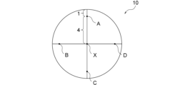
この半導体膜は、膜表面の、半導体膜の外周縁に内接する最大円(以下、最大内接円という)の中心点X並びに4つの外周点A、B、C及びDの各々において、レーザーラマン分光法により測定される、半導体膜のラマンスペクトルにおける250cm-1付近のピークの半値幅が10cm-1以下であるのが好ましい。このとき、外周点A、B、C及びDが、i)外周点A及び外周点Cを結ぶ直線と、外周点B及び外周点Dを結ぶ直線とが中心点Xで直角に交わり、かつ、ii)外周点A、B、C及びDの半導体膜の外縁からの各最短距離が半導体膜の半径の1/5となるように定められる。また、この半導体膜は円形状であるのが好ましく、その場合は図1に示されるように半導体膜10の最大内接円は外周縁と一致しうる。このように互いに十分に離れた5点においてラマンスペクトルにおける250cm-1付近のピークの半値幅が10cm-1以下であるε-Ga2O3系半導体膜は、膜の中心部から外周部に至るまでの広範囲にわたって、上記半値幅が小さいものということができ、そのような半導体膜は結晶性が高く不純物濃度が低い。
It is preferable that the half-width of the peak near 250 cm −1 in the Raman spectrum of the semiconductor film measured by laser Raman spectroscopy is 10 cm −1 or less at the center point X of the maximum circle (hereinafter referred to as the maximum inscribed circle) inscribed in the outer periphery of the semiconductor film on the film surface and at each of the four outer periphery points A, B, C, and D. In this case, the outer periphery points A, B, C, and D are determined such that i) a straight line connecting the outer periphery points A and C and a straight line connecting the outer periphery points B and D intersect at a right angle at the center point X, and ii) each of the shortest distances from the outer periphery of the semiconductor film to the outer periphery points A, B, C, and D is 1/5 of the radius of the semiconductor film. In addition, it is preferable that the semiconductor film is circular, and in that case, the maximum inscribed circle of the
本発明の半導体膜は、ラマンスペクトルにおける250cm-1付近のピークの半値幅が10cm-1以下であり、好ましくは8.0cm-1以下であり、より好ましくは7.0cm-1以下である。不純物濃度の低減の観点から、ラマンスペクトルにおける250cm-1付近のピークの半値幅は小さければ小さい方が良いため、ラマンスペクトルにおける250cm-1付近のピークの半値幅の下限値は特に限定されないが、典型的には0.1cm-1以上、より典型的には1.0cm-1以上である。 The semiconductor film of the present invention has a half-width of a peak near 250 cm −1 in a Raman spectrum of 10 cm −1 or less, preferably 8.0 cm −1 or less, and more preferably 7.0 cm −1 or less. From the viewpoint of reducing the impurity concentration, the smaller the half-width of a peak near 250 cm −1 in a Raman spectrum, the better. Therefore, the lower limit of the half-width of a peak near 250 cm −1 in a Raman spectrum is not particularly limited, but is typically 0.1 cm −1 or more, more typically 1.0 cm −1 or more.
本発明の半導体膜は、(好ましくは最大内接円の中心点X並びに外周点A、B、C及びDの各々における)ラマンスペクトルにおいて、250cm-1付近でのピーク強度I250の、260cm-1付近でのピーク強度I260に対するピーク強度比I250/I260が、2.0以上であるのが好ましく、より好ましくは5.0以上であり、さらに好ましくは8.0以上である。I250/I260は、高い方が良いためその上限値は特に限定されないが、典型的には50以下である。ここで、「260cm-1付近」とは、典型的には250cm-1付近でのピークの波数に10cm-1を足した波数を意味する。例えば、250cm-1付近のピークのピークトップが245cm-1であった場合、「260cm-1付近」のピークとは255cm-1のピークを意味する。 In the semiconductor film of the present invention, in the Raman spectrum (preferably at the center point X and the outer periphery points A, B, C, and D of the maximum inscribed circle), the peak intensity ratio I 250 /I 260 of the peak intensity I 250 near 250 cm -1 to the peak intensity I 260 near 260 cm -1 is preferably 2.0 or more, more preferably 5.0 or more, and even more preferably 8.0 or more. The higher the I 250 /I 260 , the better, so the upper limit is not particularly limited, but is typically 50 or less. Here, "near 260 cm -1 " typically means the wave number of the peak near 250 cm -1 plus 10 cm -1 . For example, if the peak top of the peak near 250 cm -1 is 245 cm -1 , the peak "near 260 cm -1 " means the peak at 255 cm -1 .
本発明の半導体膜は、(好ましくは最大内接円の中心点X並びに外周点A、B、C及びDの各々における)ラマンスペクトルにおける113cm-1付近のピークの半値幅が10cm-1以下であるのが好ましく、より好ましくは8.0cm-1以下であり、さらに好ましくは6.0cm-1以下である。不純物濃度の低減の観点から、ラマンスペクトルにおける113cm-1付近のピークの半値幅は小さければ小さい方が良いため、ラマンスペクトルにおける113cm-1付近のピークの半値幅の下限値は特に限定されないが、典型的には0.1cm-1以上、より典型的には1.0cm-1以上である。 In the semiconductor film of the present invention, the half width of the peak near 113 cm −1 in the Raman spectrum (preferably at each of the center point X and the outer periphery points A, B, C, and D of the maximum inscribed circle) is preferably 10 cm −1 or less, more preferably 8.0 cm −1 or less, and even more preferably 6.0 cm −1 or less. From the viewpoint of reducing the impurity concentration, the smaller the half width of the peak near 113 cm −1 in the Raman spectrum, the better, so the lower limit of the half width of the peak near 113 cm −1 in the Raman spectrum is not particularly limited, but is typically 0.1 cm −1 or more, more typically 1.0 cm −1 or more.
上述したように、特にFe、Ti等の遷移金属元素、Na等のアルカリ金属、F等のハロゲン元素が半導体膜に含まれると、半導体膜の諸特性のバラツキが生じやすい。この点、本発明の半導体膜は結晶性が高いため含まれうる不純物を少なくすることができる。すなわち、半導体膜の表面のTi濃度は1.0×1015atoms/cm3以下であるのが好ましく、より好ましくは1.0×1014atoms/cm3以下、さらに好ましくは1.0×1013atoms/cm3以下である。半導体膜の表面のFe濃度は1.0×1015atoms/cm3以下であるのが好ましく、より好ましくは1.0×1014atoms/cm3以下、さらに好ましくは1.0×1013atoms/cm3以下である。半導体膜の表面のNa濃度は2.0×1013atoms/cm3以下であるのが好ましく、より好ましくは1.0×1012atoms/cm3以下、さらに好ましくは1.0×1011atoms/cm3以下である。半導体膜の表面のF濃度は2.0×1015atoms/cm3以下であるのが好ましく、より好ましくは1.0×1014atoms/cm3以下、さらに好ましくは1.0×1013atoms/cm3以下である。同様に、半導体膜の表面のSi濃度は1.0×1016atoms/cm3以下であるのが好ましく、より好ましくは1.0×1015atoms/cm3以下、さらに好ましくは1.0×1014atoms/cm3以下である。半導体膜表面におけるTi、Fe、Na、F及びSiの各元素の濃度は低い方が良いため、その下限は特に限定されない。 As described above, when the semiconductor film contains transition metal elements such as Fe and Ti, alkali metals such as Na, and halogen elements such as F, the semiconductor film is likely to have variations in its characteristics. In this respect, the semiconductor film of the present invention has high crystallinity, so that the amount of impurities that can be contained can be reduced. That is, the Ti concentration on the surface of the semiconductor film is preferably 1.0×10 15 atoms/cm 3 or less, more preferably 1.0×10 14 atoms/cm 3 or less, and even more preferably 1.0×10 13 atoms/cm 3 or less. The Fe concentration on the surface of the semiconductor film is preferably 1.0×10 15 atoms/cm 3 or less, more preferably 1.0×10 14 atoms/cm 3 or less, and even more preferably 1.0×10 13 atoms/cm 3 or less. The Na concentration of the surface of the semiconductor film is preferably 2.0×10 13 atoms/cm 3 or less, more preferably 1.0×10 12 atoms/cm 3 or less, and even more preferably 1.0×10 11 atoms/cm 3 or less. The F concentration of the surface of the semiconductor film is preferably 2.0×10 15 atoms/cm 3 or less, more preferably 1.0×10 14 atoms/cm 3 or less, and even more preferably 1.0×10 13 atoms/cm 3 or less. Similarly, the Si concentration of the surface of the semiconductor film is preferably 1.0×10 16 atoms/cm 3 or less, more preferably 1.0×10 15 atoms/cm 3 or less, and even more preferably 1.0×10 14 atoms/cm 3 or less. Since it is better for the concentrations of each of the elements Ti, Fe, Na, F and Si in the semiconductor film surface to be low, there is no particular lower limit.
もっとも、Siは半導体膜へのドーパントとして用いられることもあり、その場合、半導体膜の表面のSi濃度は上記好ましい範囲の上限を超えてもよく、例えば1.0×10¹⁵~1.0×10²¹atoms/cm3でありうる。 However, Si may be used as a dopant for the semiconductor film, in which case the Si concentration at the surface of the semiconductor film may exceed the upper limit of the above preferred range, and may be, for example, 1.0×10 15 to 1.0×10 21 atoms/cm 3 .
上述のとおり、本発明の半導体膜は、ε-Ga2O3、又はε-Ga2O3系固溶体で構成される結晶を主相とするものである。本明細書において「ε-Ga2O3、又はε-Ga2O3系固溶体で構成される結晶を主相とする」とは、ε-Ga2O3、又はε-Ga2O3系固溶体で構成される結晶が半導体膜の80重量%以上、好ましくは90重量%以上、より好ましくは95重量%以上、さらに好ましくは97重量%以上、特に好ましくは99重量%以上、最も好ましくは100重量%を占めていることを意味する。ε-Ga2O3系固溶体は、ε-Ga2O3に他の成分が固溶したものである。例えば、本発明の半導体膜は、ε-Ga2O3に、Cr2O3、Fe2O3、Ti2O3、V2O3、Ir2O3、Rh2O3、In2O3及びAl2O3からなる群から選択される1種以上の成分が固溶したε-Ga2O3系固溶体で構成されるものとすることができる。また、これらの成分を固溶させることで半導体膜のバンドギャップ、電気特性、及び/又は格子定数を制御することが可能となる。これらの成分の固溶量は所望の特性に合わせて適宜変更することができる。また、ε-Ga2O3系固溶体には、その他の成分として、Si、Sn、Ge、N、Mg等の元素がドーパントとして含まれていてもよい。 As described above, the semiconductor film of the present invention has a crystal composed of ε-Ga 2 O 3 or ε-Ga 2 O 3 solid solution as a main phase. In this specification, "having a crystal composed of ε-Ga 2 O 3 or ε-Ga 2 O 3 solid solution as a main phase" means that the crystal composed of ε-Ga 2 O 3 or ε-Ga 2 O 3 solid solution accounts for 80% by weight or more of the semiconductor film, preferably 90% by weight or more, more preferably 95% by weight or more, even more preferably 97% by weight or more, particularly preferably 99% by weight or more, and most preferably 100% by weight. The ε-Ga 2 O 3 solid solution is a solid solution of ε-Ga 2 O 3 with other components. For example, the semiconductor film of the present invention may be composed of an ε-Ga 2 O 3 solid solution in which one or more components selected from the group consisting of Cr 2 O 3 , Fe 2 O 3 , Ti 2 O 3 , V 2 O 3 , Ir 2 O 3 , Rh 2 O 3 , In 2 O 3 and Al 2 O 3 are dissolved in ε-Ga 2 O 3. By dissolving these components in solid solution, it becomes possible to control the band gap, electrical characteristics and/or lattice constant of the semiconductor film. The amount of these components dissolved in solid solution can be appropriately changed according to the desired characteristics. In addition, the ε-Ga 2 O 3 solid solution may contain other components such as Si, Sn, Ge, N, Mg, etc. as dopants.
ところで、ε-Ga2O3の結晶構造は、現在の技術水準では十分に解明されていないこともあり、結晶構造解析で、κ-Ga2O3と同定されるものがε-Ga2O3としても同定されたり、あるいはε-Ga2O3と同定されるものがκ-Ga2O3としても同定されたりすることが起こりうる。例えば、非特許文献3(Ildiko Cora et al., "The real structure of ε-Ga2O3 and its relation to κ-phase," CrystEngComm, 2017, 19, 1509-1516)には、プローブ技術の分解能によっては、ε-Ga2O3の結晶構造(六方晶)とκ-Ga2O3の結晶構造(直方晶)とが混同される可能性があることが示唆されている。したがって、本明細書において「ε-Ga2O3」という用語は、ε-Ga2O3のみを指すものではなく、κ-Ga2O3をも指すものとする。すなわち、本明細書において、κ-Ga2O3の結晶構造を有すると同定されるものであっても、「ε-Ga2O3」とみなすものとし、「ε-Ga2O3」なる用語に包含されるものとする。 However, the crystal structure of ε-Ga 2 O 3 has not been fully elucidated at the current technical level, and it may happen that what is identified as κ-Ga 2 O 3 in the crystal structure analysis is also identified as ε-Ga 2 O 3 , or what is identified as ε-Ga 2 O 3 is also identified as κ-Ga 2 O 3. For example, Non-Patent Document 3 (Ildiko Cora et al., "The real structure of ε-Ga 2 O 3 and its relation to κ-phase," CrystEngComm, 2017, 19, 1509-1516) suggests that the crystal structure of ε-Ga 2 O 3 (hexagonal crystal) and the crystal structure of κ-Ga 2 O 3 (rectangular crystal) may be confused depending on the resolution of the probe technology. Therefore, in this specification, the term "ε-Ga 2 O 3 " refers not only to ε-Ga 2 O 3 but also to κ-Ga 2 O 3. That is, even if a material is identified as having the crystal structure of κ-Ga 2 O 3 in this specification, it is considered to be "ε-Ga 2 O 3 " and is included in the term "ε-Ga 2 O 3 ".
本発明のε-Ga2O3系半導体膜の略法線方向の配向方位は特に限定されないが、c軸配向であることが好ましい。もっとも、典型的なε-Ga2O3系半導体膜は、ε-Ga2O3、又はε-Ga2O3と異種材料の混晶で構成され、c軸及びa軸の2軸方向に配向しているものである。2軸配向している限り、ε-Ga2O3系半導体膜は、モザイク結晶であってもよい。モザイク結晶とは、明瞭な粒界は有しないが、結晶の配向方位がc軸及びa軸の一方又は両方がわずかに異なる結晶の集まりになっているものをいう。2軸配向の評価方法は、特に限定されるものではないが、例えばEBSD(Electron Back Scatter Diffraction Patterns)法やX線極点図等の公知の分析手法を用いることができる。例えば、EBSD法を用いる場合、2軸配向ε-Ga2O3膜の表面(膜面)、又は膜面と直交する断面の逆極点図マッピングを測定する。得られた逆極点図マッピングにおいて、(A)膜面の略法線方向に特定方位に配向していること、かつ、(B)法線方向と直交する略膜面内方向に略法線方向の配向方位と直交する軸に配向していること、という2つの条件を満たすときに略法線方向と略膜面方向の2軸に配向していると定義できる。言い換えると、上記2つの条件を満たしている場合に、c軸及びa軸の2軸に配向していると判断する。例えば膜面の略法線方向がc軸に配向している場合、略膜面内方向がc軸と直交する特定方位(例えばa軸)に配向していればよい。 The orientation direction of the ε-Ga 2 O 3 -based semiconductor film of the present invention in the approximately normal direction is not particularly limited, but is preferably c-axis orientation. However, a typical ε-Ga 2 O 3 -based semiconductor film is composed of ε-Ga 2 O 3 or a mixed crystal of ε-Ga 2 O 3 and a different material, and is oriented in two axes, the c-axis and the a-axis. As long as it is oriented in two axes, the ε-Ga 2 O 3 -based semiconductor film may be a mosaic crystal. A mosaic crystal is a collection of crystals that do not have clear grain boundaries, but whose orientation orientations are slightly different in one or both of the c-axis and the a-axis. The method for evaluating the biaxial orientation is not particularly limited, but known analytical methods such as EBSD (Electron Back Scatter Diffraction Patterns) method and X-ray pole figures can be used. For example, when using the EBSD method, the inverse pole figure mapping of the surface (film surface) of the biaxially oriented ε-Ga 2 O 3 film or the cross section perpendicular to the film surface is measured. In the obtained inverse pole figure mapping, when the following two conditions are satisfied: (A) the film surface is oriented in a specific direction, and (B) the film surface is oriented in an axis perpendicular to the orientation direction of the approximately normal direction in a direction perpendicular to the normal direction, the film surface can be defined as being oriented in two axes, the approximately normal direction and the approximately film surface direction. In other words, when the above two conditions are satisfied, it is determined that the film surface is oriented in two axes, the c-axis and the a-axis. For example, when the approximately normal direction of the film surface is oriented to the c-axis, the approximately film surface direction may be oriented in a specific direction (e.g., the a-axis) perpendicular to the c-axis.
本発明の半導体膜は、その外周縁に内接する最大円の直径(すなわち最大内接円)が5.08cm(2インチ)以上となるサイズを有していてもよく、最大内接円の直径は10.0cm以上であってもよい。最大内接円の直径の上限値は特に限定されないが、典型的には30.0cm以下、より典型的には20.0cm以下である。典型的な半導体膜は円形状であり、その場合は図1に示されるように半導体膜10の最大内接円の直径は半導体膜10の直径と一致しうる。なお、本明細書において、「円形状」とは、完全な円形状である必要はなく、全体として概ね円形と認識されうる略円形状であってもよい。例えば、円形の一部が結晶方位の特定又はその他の目的のために切り欠かれた形状や円形の一部にスリットが設けられた形状であってもよく、その場合は切り欠かれた外周縁やスリットを除いた外周縁に内接する最大円の直径に基づきサイズを決定すればよい。ところで、本発明の半導体膜はラマンスペクトルにおける250cm-1付近のピークの半値幅が10cm-1以下と小さいことを特徴としたものであり、中心点X並びに外周点A、B、C及びDは、半導体膜全体の代表的なピーク半値幅を評価できるよう、一つの例として便宜的に規定したものにすぎない。したがって、中心点X並びに外周点A、B、C及びDの位置を一義的に決定するため、半導体膜の形状を好ましくは円形と述べたが、半導体膜の形状が円形でなくても本質的な意味は何ら変わらない。例えば、半導体膜の形状が正方形や矩形(長方形)であっても、半導体膜の250cm-1付近のピークの半値幅が小さいものであれば本発明の半導体膜に包含される。このような形状の半導体膜においては、正方形や矩形の半導体膜を上面視したときに膜の外周縁に内接する最大円(最大内接円)を仮想円として規定し、その仮想円の中心点Xと仮想円の直径から(上述した円形状の半導体膜の場合と同様にして)外周点A、B、C及びDの位置を決定すればよい。こうして決定した中心点X並びに外周点A、B、C及びDにおける250cm-1付近のピークの半値幅を評価することで、円形状の半導体膜と同様の評価を実施することができる。なお、正方形や矩形の半導体膜の一部にスリットが設けられていたとしても、正方形や矩形の半導体膜を上面視したときに膜の外周縁に内接する最大円(最大内接円)を仮想円として規定することに変わりはない。
The semiconductor film of the present invention may have a size such that the diameter of the maximum circle inscribed in its outer periphery (i.e., the maximum inscribed circle) is 5.08 cm (2 inches) or more, and the diameter of the maximum inscribed circle may be 10.0 cm or more. The upper limit of the diameter of the maximum inscribed circle is not particularly limited, but is typically 30.0 cm or less, more typically 20.0 cm or less. A typical semiconductor film is circular, and in this case, the diameter of the maximum inscribed circle of the
本発明の半導体膜は、ドーパントとして14族元素を含むことができる。ここで、14族元素はIUPAC(国際純正・応用化学連合)が策定した周期律表による第14族元素のことであり、具体的には、炭素(C)、珪素(Si)、ゲルマニウム(Ge)、錫(Sn)及び鉛(Pb)のいずれかの元素である。半導体膜におけるドーパント(14族元素)として、C、Ge、Sn、及びPbの合計含有量は、好ましくは1.0×10¹⁵~1.0×10²¹/cm3、より好ましくは1.0×1017~1.0×1019/cm3である。これらのドーパントは膜中に均質に分布し、半導体膜の表面と裏面のドーパント濃度は同程度であることが好ましい。 The semiconductor film of the present invention may contain a Group 14 element as a dopant. Here, the Group 14 element refers to a Group 14 element according to the periodic table established by IUPAC (International Union of Pure and Applied Chemistry), specifically, any one of carbon (C), silicon (Si), germanium (Ge), tin (Sn) and lead (Pb). The total content of C, Ge, Sn and Pb as dopants (Group 14 elements) in the semiconductor film is preferably 1.0×10 15 to 1.0×10 21 /cm 3 , more preferably 1.0×10 17 to 1.0×10 19 /cm 3 . These dopants are distributed homogeneously in the film, and it is preferable that the dopant concentrations on the front and back surfaces of the semiconductor film are similar.
本発明の半導体膜の厚さは、コスト面及び要求される特性の観点から適宜調整すればよい。すなわち、厚すぎると成膜に時間がかかるため、コスト面からは極端に厚くない方が好ましい。一方、結晶品質を高くするためには、ある程度厚い膜とすることが好ましい。このように所望の特性に合わせて膜厚を適宜調整すればよい。The thickness of the semiconductor film of the present invention may be adjusted appropriately from the viewpoints of cost and the required characteristics. In other words, if the film is too thick, it takes a long time to form, so from a cost perspective it is preferable that the film is not extremely thick. On the other hand, in order to improve the crystal quality, it is preferable to have a film that is relatively thick. In this way, the film thickness may be adjusted appropriately to match the desired characteristics.
本発明の半導体膜は、膜単独の自立膜の形態であってもよい。また、成膜用下地基板上に作製した半導体膜を分離し、別の支持基板に転載してもよい。別の支持基板の材質は特に限定はないが、材料物性の観点から好適なものを選択すればよい。例えば、熱伝導率の観点では、Cu等の金属基板、SiC、AlN等のセラミックス基板等が好ましい。また、25~400℃での熱膨張率が6~13ppm/Kである基板を用いるのも好ましい。このような熱膨張率を有する支持基板を用いることで、半導体膜との熱膨張差を小さくすることができ、その結果、熱応力による半導体膜中のクラック発生や膜剥がれ等を抑制できる。このような支持基板の例としては、Cu-Mo複合金属で構成される基板が挙げられる。CuとMoの複合比率は、半導体膜との熱膨張率マッチング、熱伝導率、導電率等を勘案して、適宜選択することができる。The semiconductor film of the present invention may be in the form of a free-standing film of the film alone. Also, the semiconductor film formed on the base substrate for film formation may be separated and transferred to another support substrate. The material of the other support substrate is not particularly limited, but a suitable one may be selected from the viewpoint of material properties. For example, from the viewpoint of thermal conductivity, a metal substrate such as Cu, a ceramic substrate such as SiC or AlN, etc. are preferable. It is also preferable to use a substrate having a thermal expansion coefficient of 6 to 13 ppm/K at 25 to 400°C. By using a support substrate having such a thermal expansion coefficient, the thermal expansion difference with the semiconductor film can be reduced, and as a result, crack generation in the semiconductor film and film peeling due to thermal stress can be suppressed. An example of such a support substrate is a substrate made of a Cu-Mo composite metal. The composite ratio of Cu and Mo can be appropriately selected taking into consideration the thermal expansion coefficient matching with the semiconductor film, thermal conductivity, electrical conductivity, etc.
半導体膜の製造方法
本発明の半導体膜は、下地基板としてGaN単結晶基板を用いて、その上にε-Ga2O3系材料を成膜することにより、好ましく製造することができる。半導体層の形成手法は公知の手法が可能であるが、好ましい例としては、ミストCVD法(ミスト化学気相成長法)、HVPE法(ハライド気相成長法)、MBE法(分子線エピタキシー法)、MOCVD法(有機金属気相成長法)、及び水熱合成法が挙げられ、ミストCVD法又はHVPE法が特に好ましい。ミストCVD法やHVPE法等の気相成長法の場合、下地基板の厚さは、反りを抑制する観点では厚い方が望ましく、好ましくは0.5mm以上、より好ましくは0.8mm以上、さらに好ましくは1.4mm以上である。一方で、この厚さは、コストの観点では薄い方が望ましく、好ましくは1.0mm以下、より好ましくは0.5mm以下である。このように所望の特性に合わせて下地基板の膜さを適宜調整すればよい。下地基板の厚さの上限は特に限定されないが、典型的には5.0mm以下、より典型的には4.0mm以下である。また、膜の中心部から外周部に至るまでの広範囲にわたって250cm-1付近のピークの半値幅が10cm-1以下と小さいε-Ga2O3系半導体膜は、下地基板を回転させながら成膜を行うことにより好ましく実現することができる。 Manufacturing method of semiconductor film The semiconductor film of the present invention can be preferably manufactured by using a GaN single crystal substrate as a base substrate and forming a film of an ε-Ga 2 O 3 -based material thereon. The semiconductor layer can be formed by a known method, but preferred examples include mist CVD (mist chemical vapor deposition), HVPE (halide vapor phase epitaxy), MBE (molecular beam epitaxy), MOCVD (metal organic vapor phase epitaxy), and hydrothermal synthesis, with mist CVD or HVPE being particularly preferred. In the case of vapor phase epitaxy such as mist CVD or HVPE, the thickness of the base substrate is preferably thicker from the viewpoint of suppressing warping, and is preferably 0.5 mm or more, more preferably 0.8 mm or more, and even more preferably 1.4 mm or more. On the other hand, this thickness is preferably thinner from the viewpoint of cost, and is preferably 1.0 mm or less, and more preferably 0.5 mm or less. In this way, the thickness of the base substrate may be appropriately adjusted according to the desired characteristics. The upper limit of the thickness of the base substrate is not particularly limited, but is typically 5.0 mm or less, more typically 4.0 mm or less. In addition, an ε-Ga 2 O 3 -based semiconductor film having a small half-width of the peak near 250 cm −1 of 10 cm −1 or less over a wide range from the center to the outer periphery of the film can be preferably realized by forming the film while rotating the base substrate.
以下、特に好ましい成膜方法であるHVPE法及びミストCVD法について説明する。 Below, we will explain the HVPE method and the mist CVD method, which are particularly preferred film formation methods.
HVPE法(ハライド気相成長法)はCVDの一種であり、Ga2O3やGaN等の化合物半導体の成膜に適用可能な方法である。この方法では、Ga原料とハロゲン化物を反応させてハロゲン化ガリウムガスを発生させ、成膜用下地基板上に供給する。同時にO2ガスを成膜用下地基板上に供給し、ハロゲン化ガリウムガスとO2ガスが反応することで成膜用下地基板上にGa2O3が成長する。高速及び厚膜成長が可能であり、工業的にも広く実績を有する方法であり、ε-Ga2O3だけでなくα-Ga2O3、β-Ga2O3の成膜例が報告されている。 The HVPE method (halide vapor phase epitaxy) is a type of CVD and is a method applicable to the deposition of compound semiconductors such as Ga 2 O 3 and GaN. In this method, a Ga raw material is reacted with a halide to generate gallium halide gas, which is then supplied onto a substrate for deposition. At the same time, O 2 gas is supplied onto the substrate for deposition, and the gallium halide gas and O 2 gas react with each other to grow Ga 2 O 3 on the substrate for deposition. This method allows high-speed and thick film growth and has a wide track record in the industrial field, and examples of deposition of not only ε-Ga 2 O 3 but also α-Ga 2 O 3 and β-Ga 2 O 3 have been reported.
図2にHVPE法を用いた気相成長装置(HVPE装置)の一例を示す。HVPE装置20は、リアクタ22と、成膜用下地基板24を載置するサセプタ26と、酸素原料供給源30と、キャリアガス供給源28と、GeCl4供給源32と、Ga原料供給源34と、ヒータ36と、ガス排出部38を備えている。リアクタ22は、原料と反応しない任意のリアクタが適用され、例えば石英管である。ヒータ36は少なくとも700℃(好ましくは900℃以上)まで加熱可能な任意のヒータが適用され、例えば抵抗加熱式のヒータである。
2 shows an example of a vapor phase growth apparatus (HVPE apparatus) using the HVPE method. The
Ga原料供給源34には内部に金属Gaが載置されており、ハロゲンガス又はハロゲン化水素ガス、例えばHClが供給される。ハロゲンガス又はハロゲン化ガスは好ましくはCl2又はHClである。供給されたハロゲンガス又はハロゲン化ガスは金属Gaと反応し、ハロゲン化ガリウムガスが生じ、成膜用下地基板24に供給される。ハロゲン化ガリウムガスは、好ましくはGaCl及び又はGaCl3を含む。酸素原料供給源30は、O2、H2O及びN2Oからなる群から選択される酸素源が供給可能だが、O2が好ましい。これらの酸素原料ガスは、ハロゲン化ガリウムガスと同時に下地基板に供給される。GeCl4供給源32は、GeCl4液体をバブリングして発生するGeCl4蒸気をリアクタ22内に供給する。なお、Ga原料や酸素原料ガスはN2や希ガス等のキャリアガスとともに供給してもよい。
The
ガス排出部38は、例えば、拡散ポンプ、ロータリーポンプ等の真空ポンプに接続されていてもよく、リアクタ22内の未反応のガスの排出だけでなく、リアクタ22内を減圧下に制御してもよい。これにより、気相反応の抑制、及び成長速度分布が改善され得る。The
ヒータ36を用いて所定の温度まで成膜用下地基板24を加熱し、ハロゲン化ガリウムガスと酸素原料ガスを同時に供給することで、成膜用下地基板24上にε-Ga2O3が形成される。成膜温度はε-Ga2O3が成膜され、膜中の不純物が少なくなる限り特に限定されないが、例えば250℃~900℃が典型的である。Ga原料ガスや酸素原料ガスの分圧も特に限定はされない。例えば、Ga原料ガス(ハロゲン化ガリウムガス)の分圧は0.05kPa以上10kPa以下の範囲としてもよく、酸素原料ガスの分圧は0.25kPa以上50kPa以下の範囲としてもよい。
The
ドーパントとして14族元素を含有するε-Ga2O3系半導体膜を成膜する場合や、InやAlの酸化物等を含むε-Ga2O3との混晶膜を成膜する場合は、別途供給源(例えば図2ではGeCl4供給源32)を設けてそれらのハロゲン化物等を供給してもよいし、Ga原料供給源34からハロゲン化物を混合して供給してもよい。また、金属Gaと同じ箇所に14族元素やIn、Al等を含有する材料を載置し、ハロゲンガス又はハロゲン化水素ガスと反応させ、ハロゲン化物として供給してもよい。成膜用下地基板24に供給されたそれらのハロゲン化物ガスは、ハロゲン化ガリウムと同様、酸素原料ガスと反応して酸化物となり、ε-Ga2O3系半導体膜中に取り込まれる。
When forming an ε-Ga 2 O 3 based semiconductor film containing a group 14 element as a dopant, or when forming a mixed crystal film with ε-Ga 2 O 3 containing oxides of In or Al, a separate supply source (for example, a GeCl 4 supply source 32 in FIG. 2) may be provided to supply the halide or the like, or a mixture of halides may be supplied from a Ga raw
ミストCVD法は、原料溶液を霧化又は液滴化してミスト又は液滴を発生させ、キャリアガスを用いてミスト又は液滴を基板を備えた成膜室に搬送し、成膜室内でミスト又は液滴を熱分解及び化学反応させて基板上に膜を形成及び成長させる手法であり、真空プロセスを必要とせず、短時間で大量のサンプルを作製することができる。図3にミストCVD装置の一例を示す。図3に示されるミストCVD装置40は、キャリアガスG及び原料溶液LからミストMを発生させるミスト発生室42と、ミストMを基板56に吹き付けて熱分解及び化学反応を経て半導体膜58を形成する成膜室50とを有する。ミスト発生室42は、キャリアガスGが導入されるキャリアガス導入口44と、ミスト発生室42内に設けられる超音波振動子46と、ミスト発生室42内で発生したミストMを成膜室50に搬送するダクト48とを備えている。ミスト発生室42内には原料溶液Lが収容される。超音波振動子46は、原料溶液Lに超音波振動を与えてキャリアガスGとともにミストMを発生できるように構成される。成膜室50は、ダクト48を介して導入されるミストMを基板56に吹き付けるためのノズル52と、基板56が固定されるステージ54と、ステージ54の裏面近傍に設けられてステージ54及び基板56を加熱するためのヒータ62と、キャリアガスGを排出するための排気口64とを備える。The mist CVD method is a method in which a raw material solution is atomized or turned into droplets to generate mist or droplets, and the mist or droplets are transported to a film-forming chamber equipped with a substrate using a carrier gas, and the mist or droplets are thermally decomposed and chemically reacted in the film-forming chamber to form and grow a film on the substrate. This method does not require a vacuum process and can produce a large number of samples in a short time. Figure 3 shows an example of a mist CVD apparatus. The
ミストCVD法に用いる原料溶液Lとしては、ε-Ga2O3系半導体膜が得られる溶液であれば、限定されるものではないが、例えば、Ga及び/又はGaと固溶体を形成する金属の有機金属錯体やハロゲン化物を溶媒に溶解させたものが挙げられる。有機金属錯体の例としては、アセチルアセトナート錯体が挙げられる。また、半導体層にドーパントを加える場合には、原料溶液にドーパント成分の溶液を加えてもよい。さらに、原料溶液には塩酸等の添加剤を加えてもよい。溶媒としては水やアルコール等を使用することができる。 The raw material solution L used in the mist CVD method is not limited as long as it is a solution that can obtain an ε-Ga 2 O 3 -based semiconductor film, but examples thereof include organometallic complexes and halides of Ga and/or metals that form solid solutions with Ga dissolved in a solvent. An example of an organometallic complex is an acetylacetonate complex. In addition, when a dopant is added to the semiconductor layer, a solution of a dopant component may be added to the raw material solution. Furthermore, an additive such as hydrochloric acid may be added to the raw material solution. Water, alcohol, etc. can be used as the solvent.
次に、得られた原料溶液Lを霧化又は液滴化してミストM又は液滴を発生させる。霧化又は液滴化する方法の好ましい例としては、超音波振動子46を用いて原料溶液Lを振動させる手法が挙げられる。その後、得られたミストM又は液滴を、キャリアガスGを用いて成膜室50に搬送する。キャリアガスGとしては特に限定されるものではないが、酸素、オゾン、窒素等の不活性ガス、及び水素等の還元ガスの一種又は二種以上を用いることができる。Next, the obtained raw material solution L is atomized or turned into droplets to generate mist M or droplets. A preferred example of a method for atomizing or turning into droplets is a technique in which the raw material solution L is vibrated using an
成膜室50には基板56が備えられている。成膜室50に搬送されたミストM又は液滴は、そこで熱分解及び化学反応されて、基板56上に半導体膜58を形成する。反応温度は原料溶液Lの種類に応じて異なるが、好ましくは300~800℃、より好ましくは400~700℃である。また、成膜室50内の雰囲気は、所望の半導体膜が得られる限り特に限定されるものではなく、典型的には、酸素ガス雰囲気、不活性ガス雰囲気、真空雰囲気、還元雰囲気、及び大気雰囲気のいずれかから選択される。The
このようにして得られた半導体膜は、そのままの形態又は分割して半導体素子とすることが可能である。あるいは、半導体膜を下地基板から剥離して膜単体の形態としてもよい。この場合、下地基板からの剥離を容易にするために、下地基板の表面(成膜面)に予め剥離層を設けたものを用いてもよい。このような剥離層は、下地基板表面にC注入層やH注入層を設けたものが挙げられる。また、半導体膜の成膜初期にCやHを膜中に注入させ、半導体膜側に剥離層を設けてもよい。さらに、下地基板上に成膜された半導体膜の表面(すなわち下地基板とは反対側の面)に下地基板とは異なる支持基板(実装基板)を接着及び接合し、その後、半導体膜から下地基板を剥離除去することも可能である。このような支持基板(実装基板)として、25~400℃での熱膨張率が6~13ppm/Kであるもの、例えばCu-Mo複合金属で構成される基板を用いることができる。また、半導体膜と支持基板(実装基板)を接着及び接合する手法の例としては、ロウ付け、半田、固相接合等の公知の手法を挙げることができる。さらに、半導体膜と支持基板との間に、オーミック電極、ショットキー電極等の電極、又は接着層等の他の層を設けてもよい。The semiconductor film thus obtained can be used as it is or divided into a semiconductor element. Alternatively, the semiconductor film may be peeled off from the base substrate to form a single film. In this case, a peeling layer may be provided on the surface (film formation surface) of the base substrate in advance to facilitate peeling from the base substrate. Examples of such a peeling layer include a C-injected layer or an H-injected layer provided on the surface of the base substrate. Alternatively, C or H may be injected into the film at the initial stage of the semiconductor film formation, and a peeling layer may be provided on the semiconductor film side. Furthermore, it is also possible to bond and attach a support substrate (mounting substrate) different from the base substrate to the surface of the semiconductor film formed on the base substrate (i.e., the surface opposite to the base substrate), and then peel and remove the base substrate from the semiconductor film. As such a support substrate (mounting substrate), a substrate having a thermal expansion coefficient of 6 to 13 ppm/K at 25 to 400°C, for example, a substrate made of a Cu-Mo composite metal, can be used. Examples of methods for bonding and joining the semiconductor film and the support substrate (mounting substrate) include known methods such as brazing, soldering, and solid-state bonding. Furthermore, an electrode such as an ohmic electrode or a Schottky electrode, or another layer such as an adhesive layer may be provided between the semiconductor film and the supporting substrate.
パワーデバイス等の半導体素子の製造においては、半導体膜上にドリフト層等の機能層が形成されることになる。ドリフト層等の機能層の形成についても、公知の手法が可能であり、好ましい例としては、ミストCVD法、HVPE法、MBE法、MOCVD法、及び水熱合成法が挙げられ、ミストCVD法又はHVPE法が特に好ましい。In the manufacture of semiconductor elements such as power devices, functional layers such as drift layers are formed on semiconductor films. Formation of functional layers such as drift layers can be performed using known methods, and preferred examples include mist CVD, HVPE, MBE, MOCVD, and hydrothermal synthesis, with mist CVD or HVPE being particularly preferred.
複合基板
本発明の半導体膜は、下地基板として好ましくはGaN単結晶基板を用いて、その上にε-Ga2O3系材料を成膜することにより製造することができる。すなわち、本発明によれば、GaN単結晶基板と、GaN単結晶基板上に形成された上述した半導体膜とを備えた、複合基板が提供される。The semiconductor film of the present invention can be manufactured by forming a film of an ε-Ga 2 O 3 based material on a GaN single crystal substrate, which is preferably used as a base substrate. That is, the present invention provides a composite substrate comprising a GaN single crystal substrate and the above-mentioned semiconductor film formed on the GaN single crystal substrate.
本発明を以下の例によってさらに具体的に説明する。The present invention will be further illustrated by the following examples.
例1
(1)ミストCVD法によるε-Ga2O3系半導体膜の作製
(1a)下地基板の準備
下地基板として、厚さ約0.4mmで直径5.08cm(2インチ)のc面GaN単結晶基板を準備した。 Example 1
(1) Preparation of ε-Ga 2 O 3 -Based Semiconductor Film by Mist CVD Method (1a) Preparation of Base Substrate A c-plane GaN single crystal substrate having a thickness of about 0.4 mm and a diameter of 5.08 cm (2 inches) was prepared as a base substrate.
(1b)原料溶液の作製
塩酸に金属Gaを添加して室温で3週間撹拌することで、ガリウムイオン濃度が3mol/Lの塩化ガリウム溶液を得た。得られた塩化ガリウム溶液に水を加えてガリウムイオン濃度が55mmol/Lとなるように水溶液を調整した。この水溶液に水酸化アンモニウムを添加してpHを4.0となるように調整し、原料溶液とした。
(1b) Preparation of raw material solution Metal Ga was added to hydrochloric acid and stirred at room temperature for 3 weeks to obtain a gallium chloride solution with a gallium ion concentration of 3 mol/L. Water was added to the obtained gallium chloride solution to adjust the aqueous solution to a gallium ion concentration of 55 mmol/L. Ammonium hydroxide was added to this aqueous solution to adjust the pH to 4.0 to obtain a raw material solution.
(1c)成膜準備
図3に示される構成のミストCVD装置40を準備した。ミストCVD装置40の構成については前述したとおりである。ミストCVD装置40において、上記(1b)で得られた原料溶液Lをミスト発生室42内に収容した。基板56として直径5.08cm(2インチ)のc面GaN基板をステージ54にセットし、ノズル52の先端と基板56の間の距離を120mmとした。ヒータ62により、ステージ54の温度を520℃にまで昇温させ、温度安定化のため30分保持した。流量調節弁(図示せず)を開いてキャリアガスGとしての窒素ガスを、ミスト発生室42を経て成膜室50内に供給し、成膜室50の雰囲気をキャリアガスGで十分置換した。その後、キャリアガスGの流量を1.7L/minに調節した。
(1c) Film Formation Preparation A
(1d)成膜
超音波振動子46によって原料溶液Lを霧化し、発生したミストMをキャリアガスGによって成膜室50内に導入した。ミストMを成膜室50内、特に基板56(具体的にはGaN基板)の表面で反応させることによって、基板56上に半導体膜58を60分にわたって形成した。下地基板及び成膜の条件を表1に示す。
(1d) Film formation The raw material solution L was atomized by the
(2)半導体膜の評価
(2a)表面EDX
得られた膜表面のEDX測定を行った結果、Ga及びOのみが検出され、得られた膜はGa酸化物であることが分かった。
(2) Evaluation of semiconductor film (2a) Surface EDX
The surface of the obtained film was subjected to EDX measurement, and as a result, only Ga and O were detected, and it was found that the obtained film was a Ga oxide.
(2b)表面EBSD
電子線後方散乱回折装置(EBSD)(オックスフォード・インストゥルメンツ社製Nordlys Nano)を取り付けたSEM(日立ハイテクノロジーズ社製、SU-5000)にてGa酸化物膜表面の逆極点図方位マッピングを約25μm×20μmの視野で実施した。装置に付属したソフトウエア(Twist)を用いて、非特許文献4(F. Mezzadri, et al., "Crystal Structure and Ferroelectric Properties of ε-Ga2O3 Films Grown on (0001)-Sapphire," Inorg. Chem. 2016, 55, 12079-12084)に記載のε-Ga2O3(六方晶)の空間群、単位格子パラメータ(辺及び角度)、原子位置の結晶情報をデータベース登録し、これを用いてEBSD測定を行った。
(2b) Surface EBSD
Inverse pole figure orientation mapping of the Ga oxide film surface was performed using a SEM (SU-5000, Hitachi High-Technologies Corporation) equipped with an electron backscatter diffraction (EBSD) (Nordlys Nano, Oxford Instruments). The measurement was performed with a field of view of 25 μm × 20 μm. Using the software (Twist) attached to the device, the crystal structure and ferroelectric properties of ε-Ga 2 O 3 Films Grown in accordance with the method described in Non-Patent Document 4 (F. Mezzadri, et al., "Crystal Structure and Ferroelectric Properties of ε-Ga 2 O 3 Films Grown in The space group, unit cell parameters (sides and angles), and atomic positions of ε-Ga 2 O 3 (hexagonal crystal) described in "Patent Document 1: Crystal Structure of ε-Ga 2 O 3 on (0001)-Sapphire," Inorg. Chem. 2016, 55, 12079-12084" are shown. The information was entered into a database and used to perform EBSD measurements.
このEBSD測定の諸条件は以下のとおりとした。
<EBSD測定条件>
・加速電圧:15kV
・スポット強度:70
・ワーキングディスタンス:22.5mm
・ステップサイズ:0.5μm
・試料傾斜角:70°
・測定プログラム:Aztec(version 3.3)
The conditions for this EBSD measurement were as follows:
<EBSD measurement conditions>
Acceleration voltage: 15 kV
Spot Intensity: 70
Working distance: 22.5 mm
Step size: 0.5 μm
Sample tilt angle: 70°
Measurement program: Aztec (version 3.3)
得られた逆極点図方位マッピングから、Ga酸化物膜は、基板法線方向にc軸配向し、面内も配向した2軸配向の結晶構造を有することが分かった。これらの結果から、得られた半導体膜はε-Ga2O3で構成される結晶構造の配向膜であることが確認された。 From the obtained inverse pole figure orientation mapping, it was found that the Ga oxide film has a biaxially oriented crystal structure with the c-axis oriented in the normal direction of the substrate and also oriented in-plane. These results confirmed that the obtained semiconductor film is an oriented film with a crystal structure composed of ε-Ga 2 O 3 .
(2c)ラマンスペクトル
半導体膜58の膜面の中心点X、並びに外周点A、B、C及びDにおけるラマンスペクトルを、堀場製作所製レーザーラマン分光測定装置LabRAM ARAMISを用い、操作ソフトウェアLabSpec(Ver.5.78)を用いて測定した。光学系はツェルニターナ型分光系、後方散乱方式であり、光源として半導体励起固体レーザー(DPSS、532nm)を用いた。サンプルの測定前にはSiウェハを用い、校正を行った。半導体膜58に対するラマンスペクトルの測定は、レーザー出力を24mWに調整しHole(コンフォーカルホール径)を400μm、分光器の中心波数を520cm-1、Slitを100μm、グレーティングを1800gr/mm、対物レンズを100倍とし、点分析モードで行った。露光時間は60秒、積算回数を2回とし、波数範囲は100~900cm-1とした。減光フィルターは最強ピークのカウントが3000以上50000以下となるように適宜設定した。また、測定時にNeランプを使用し、得られたスペクトルに対し、Neランプ輝線に起因するピークのピークトップの波数が278.28cm-1となるように、スペクトルを補正した。ベースラインの補正は、ソフトウェアLabSpec上の機能にて「Type」を「Lines」、「Degree」を「5」、「Attach」を「No」、「Style」を「-」に設定し、「Auto」にして行った。このように得られたスペクトルを図4に示す。得られたスペクトルに対し、中心点X、並びに外周点A、B、C及びDにおける、250cm-1付近のピークのピークトップの波数をNX、NA、NB、NC及びND、並びに113cm-1付近のピークのピークトップの波数をNX、NA、NB、NC及びNDとした。また、波数NX、NA、NB、NC及びNDにおける半値幅を、WX、WA、WB、WC及びWDとした。さらに、中心点X、並びに外周点A、B、C及びDにおける、250cm-1付近にピークトップを持つピークでのピーク強度I250の、260cm-1でのピーク強度I260に対するピーク強度比I250/I260を求めた。本例では、例えば、250cm-1付近のピークのピークトップの波数NXが251.1cm-1であり、このピークに対する半値幅WXを算出したところ、8.8cm-1となり、結晶性の高いε-Ga2O3であることがわかった。結果は、表2に示されるとおりであった。
(2c) Raman spectrum The Raman spectrum at the center point X of the film surface of the
(2d)各元素の濃度
二次イオン質量分析装置(SIMS)を用いて、ε-Ga2O3の膜表面の組成分析を行い、Fe、Ti、Na、F及びSiの濃度を測定した。このD-SIMS分析の諸条件は以下のとおりとした。結果は、表2に示されるとおりであった。
(2d) Concentration of each element Using a secondary ion mass spectrometer (SIMS), the composition of the ε-Ga 2 O 3 film surface was analyzed to measure the concentrations of Fe, Ti, Na, F and Si. The conditions for this D-SIMS analysis were as follows. The results are shown in Table 2.
<D-SIMS分析条件(Fe、Ti及びNaを検出する場合)>
・注目元素:Fe、Ti、Na
・装置:CAMECA社製 IMS-7f
・一次イオン種:O22+
・一次イオン加速エネルギー:8keV
・二次イオン極性:Positive
・検出領域:直径30μm
<D-SIMS analysis conditions (when detecting Fe, Ti, and Na)>
・Elements of interest: Fe, Ti, Na
・Apparatus: CAMECA IMS-7f
Primary ion species: O2
Primary ion acceleration energy: 8 keV
Secondary ion polarity: Positive
Detection area:
<D-SIMS分析条件(F及びSiを検出する場合)>
・注目元素:F、Si
・装置:CAMECA社製 IMS-7f
・一次イオン種:Cs+
・一次イオン加速エネルギー:15.0keV
・二次イオン極性:Negative
・検出領域:直径30μm
<D-SIMS analysis conditions (when detecting F and Si)>
・Notable elements: F, Si
・Apparatus: CAMECA IMS-7f
Primary ion species: Cs +
Primary ion acceleration energy: 15.0 keV
Secondary ion polarity: Negative
Detection area:
例2
上記(1c)及び(1d)において、ミストCVD法で成膜する際に、ステージ54の温度を500℃で安定化させた上で成膜を開始すると共に、520℃まで20分間かけて昇温させたこと以外は、例1と同様にして半導体膜の作製及び各種評価を行った。250cm-1付近のピークのピークトップの波数NXが246.8cm-1であり、このピークに対する半値幅WXを算出したところ、6.7cm-1となった。このことから、250cm-1付近のピークはシャープなピークであることが分かった。また、この半導体膜は不純物濃度が低かった。結果は、表1及び2に示されるとおりであった。 Example 2
In the above (1c) and (1d), when forming a film by mist CVD, the temperature of the
例3
ミストCVD法(上記(1))の代わりに、以下に説明するHVPE法によりε-Ga2O3系半導体膜を作製したこと以外は、例1と同様にして各種評価を行った。250cm-1付近のピークのピークトップの波数NXが248.3cm-1であり、このピークに対する半値幅WXを算出したところ、7.0cm-1となった。このことから、250cm-1付近のピークはシャープなピークであることが分かった。また、この半導体膜は不純物濃度が低かった。結果は、表1及び2に示されるとおりであった。 Example 3
Various evaluations were performed in the same manner as in Example 1, except that an ε-Ga 2 O 3 -based semiconductor film was produced by the HVPE method described below instead of the mist CVD method (above (1)). The wave number N X of the peak top of the peak near 250 cm -1 was 248.3 cm -1 , and the half-width W X for this peak was calculated to be 7.0 cm -1 . From this, it was found that the peak near 250 cm -1 was a sharp peak. In addition, this semiconductor film had a low impurity concentration. The results were as shown in Tables 1 and 2.
(1’)HVPE法によるε-Ga2O3系半導体膜の作製
(1a’)下地基板の準備
下地基板として、厚さ約0.4mmで直径5.08cm(2インチ)のc面GaN単結晶基板を準備した。
(1') Preparation of ε-Ga 2 O 3 -based semiconductor film by HVPE method (1a') Preparation of base substrate A c-plane GaN single crystal substrate with a thickness of about 0.4 mm and a diameter of 5.08 cm (2 inches) was prepared as a base substrate.
(1b’)成膜
図2に示される構成のHVPE装置20を準備した。HVPE装置20の構成については前述したとおりである。金属Gaをリアクタ22内に配置し、塩化水素ガス(HCl)を供給した。これにより金属Gaと塩化水素を反応させてGaのハロゲン化物を生成させて、成膜用下地基板24へ供給した。同時に、酸素原料としてのO2ガス及びキャリアガスとしてN2ガスをリアクタ22内に導入した。こうしてHVPE法による成膜を550℃の成長温度で15分間行い、成膜用下地基板24及びその上に形成された半導体膜を複合材料として得た。
(1b') Film formation An
例4
HVPE法における上記(1b’)において、成長温度を550℃で安定化させた上で成膜を開始すると共に、580℃まで30分間かけて昇温させたこと以外は、例3と同様にして半導体膜の作製及び各種評価を行った。250cm-1付近のピークのピークトップの波数NXが254.9cm-1であり、このピークに対する半値幅WXを算出したところ、5.9cm-1となった。このことから、250cm-1付近のピークはシャープなピークであることが分かった。また、この半導体膜は不純物濃度が低かった。結果は、表1及び2に示されるとおりであった。 Example 4
In the above (1b') in the HVPE method, the growth temperature was stabilized at 550°C before starting the film formation, and the temperature was raised to 580°C over 30 minutes. Except for this, the semiconductor film was produced and various evaluations were performed in the same manner as in Example 3. The wave number N X of the peak top of the peak near 250 cm -1 was 254.9 cm -1 , and the half-width W X for this peak was calculated to be 5.9 cm -1 . From this, it was found that the peak near 250 cm -1 was a sharp peak. In addition, this semiconductor film had a low impurity concentration. The results were as shown in Tables 1 and 2.
例5(比較)
ミストCVD法における上記(1c)及び(1d)において、成膜する際に、ステージ54の温度を500℃で安定化させたこと以外は、例1と同様にして半導体膜の作製及び各種評価を行った。250cm-1付近のピークのピークトップの波数NXが251.9cm-1であり、このピークに対する半値幅WXを算出したところ、16.5cm-1となった。このことから、250cm-1付近のピークはブロードなピークであることが分かった。また、この半導体膜は不純物濃度が高かった。結果は、表1及び2に示されるとおりであった。 Example 5 (Comparison)
In the mist CVD method (1c) and (1d) above, the temperature of the
例6(比較)
HVPE法における上記(1b’)において、成長温度を500℃で安定化させたこと以外は、例3と同様にして半導体膜の作製及び各種評価を行った。250cm-1付近のピークのピークトップの波数NXが251.7cm-1であり、このピークに対する半値幅WXを算出したところ、14.3cm-1となった。このことから、250cm-1付近のピークはブロードなピークであることが分かった。また、この半導体膜は不純物濃度が高かった。結果は、表1及び2に示されるとおりであった。 Example 6 (Comparison)
In the above (1b') in the HVPE method, except that the growth temperature was stabilized at 500° C., the semiconductor film was produced and various evaluations were performed in the same manner as in Example 3. The wave number N X of the peak top of the peak near 250 cm −1 was 251.7 cm −1 , and the half-width W X for this peak was calculated to be 14.3 cm −1 . From this, it was found that the peak near 250 cm −1 was a broad peak. In addition, this semiconductor film had a high impurity concentration. The results were as shown in Tables 1 and 2.


Claims (9)
レーザーラマン分光法により測定される、前記半導体膜のラマンスペクトルにおける250cm-1付近のピークの半値幅が10cm-1以下であり、
前記半導体膜の表面の、前記半導体膜の外周縁に内接する最大円の中心点X並びに4つの外周点A、B、C及びDの各々において、レーザーラマン分光法により測定される、前記半導体膜のラマンスペクトルにおける250cm -1 付近のピークの半値幅が10cm -1 以下であり、
前記外周点A、B、C及びDが、i)前記外周点A及び前記外周点Cを結ぶ直線と、前記外周点B及び前記外周点Dを結ぶ直線とが前記中心点Xで直角に交わり、かつ、ii)前記外周点A、B、C及びDの前記半導体膜の外縁からの各最短距離が前記半導体膜の半径の1/5となるように定められ、
前記半導体膜は、前記半導体膜の外周縁に内接する最大円の直径が5.08cm以上となるサイズを有する、半導体膜。 A semiconductor film having a crystal phase mainly composed of ε-Ga 2 O 3 or an ε-Ga 2 O 3 solid solution,
the half-width of a peak at about 250 cm −1 in a Raman spectrum of the semiconductor film measured by laser Raman spectroscopy is 10 cm −1 or less ;
the half-width of a peak near 250 cm −1 in a Raman spectrum of the semiconductor film measured by laser Raman spectroscopy at a center point X of the largest circle inscribed in the outer periphery of the semiconductor film and at each of four outer periphery points A, B, C and D on the surface of the semiconductor film is 10 cm −1 or less,
the outer periphery points A, B, C, and D are determined such that i) a straight line connecting the outer periphery points A and C and a straight line connecting the outer periphery points B and D intersect at a right angle at the center point X, and ii) the shortest distance from the outer edge of the semiconductor film to each of the outer periphery points A, B, C, and D is 1/5 of the radius of the semiconductor film;
The semiconductor film has a size such that the diameter of the maximum circle inscribed on the outer periphery of the semiconductor film is 5.08 cm or more .
Applications Claiming Priority (3)
| Application Number | Priority Date | Filing Date | Title |
|---|---|---|---|
| JP2021139270 | 2021-08-27 | ||
| JP2021139270 | 2021-08-27 | ||
| PCT/JP2022/023323 WO2023026633A1 (en) | 2021-08-27 | 2022-06-09 | Semiconductor film and composite substrate |
Publications (2)
| Publication Number | Publication Date |
|---|---|
| JPWO2023026633A1 JPWO2023026633A1 (en) | 2023-03-02 |
| JP7620719B2 true JP7620719B2 (en) | 2025-01-23 |
Family
ID=85321722
Family Applications (1)
| Application Number | Title | Priority Date | Filing Date |
|---|---|---|---|
| JP2023543703A Active JP7620719B2 (en) | 2021-08-27 | 2022-06-09 | Semiconductor film and composite substrate |
Country Status (2)
| Country | Link |
|---|---|
| JP (1) | JP7620719B2 (en) |
| WO (1) | WO2023026633A1 (en) |
Citations (7)
| Publication number | Priority date | Publication date | Assignee | Title |
|---|---|---|---|---|
| JP2017007871A (en) | 2015-06-16 | 2017-01-12 | 国立研究開発法人物質・材料研究機構 | ε-Ga2O3 single crystal, ε-Ga2O3 manufacturing method, and semiconductor device using the same |
| JP2019009405A (en) | 2017-06-28 | 2019-01-17 | 株式会社Flosfia | Laminate structure and semiconductor device |
| JP2019012826A (en) | 2017-06-30 | 2019-01-24 | 国立研究開発法人物質・材料研究機構 | Gallium nitride semiconductor substrate, gallium nitride semiconductor device, imaging device, and manufacturing method thereof |
| JP2019142756A (en) | 2018-02-22 | 2019-08-29 | トヨタ自動車株式会社 | Film deposition method |
| JP2020011859A (en) | 2018-07-17 | 2020-01-23 | トヨタ自動車株式会社 | Film deposition method, and manufacturing method of semiconductor device |
| WO2021048950A1 (en) | 2019-09-11 | 2021-03-18 | 日本碍子株式会社 | Semiconductor film |
| CN113066902A (en) | 2021-03-25 | 2021-07-02 | 北京邮电大学 | Method for regulating and controlling photoelectric response performance of epsilon-phase gallium oxide through oxygen vacancy concentration |
-
2022
- 2022-06-09 WO PCT/JP2022/023323 patent/WO2023026633A1/en not_active Ceased
- 2022-06-09 JP JP2023543703A patent/JP7620719B2/en active Active
Patent Citations (7)
| Publication number | Priority date | Publication date | Assignee | Title |
|---|---|---|---|---|
| JP2017007871A (en) | 2015-06-16 | 2017-01-12 | 国立研究開発法人物質・材料研究機構 | ε-Ga2O3 single crystal, ε-Ga2O3 manufacturing method, and semiconductor device using the same |
| JP2019009405A (en) | 2017-06-28 | 2019-01-17 | 株式会社Flosfia | Laminate structure and semiconductor device |
| JP2019012826A (en) | 2017-06-30 | 2019-01-24 | 国立研究開発法人物質・材料研究機構 | Gallium nitride semiconductor substrate, gallium nitride semiconductor device, imaging device, and manufacturing method thereof |
| JP2019142756A (en) | 2018-02-22 | 2019-08-29 | トヨタ自動車株式会社 | Film deposition method |
| JP2020011859A (en) | 2018-07-17 | 2020-01-23 | トヨタ自動車株式会社 | Film deposition method, and manufacturing method of semiconductor device |
| WO2021048950A1 (en) | 2019-09-11 | 2021-03-18 | 日本碍子株式会社 | Semiconductor film |
| CN113066902A (en) | 2021-03-25 | 2021-07-02 | 北京邮电大学 | Method for regulating and controlling photoelectric response performance of epsilon-phase gallium oxide through oxygen vacancy concentration |
Non-Patent Citations (1)
| Title |
|---|
| 森本 尚太 他,ミストCVD法による塩化物原料を用いたGaNテンプレート上へのε-Ga2O3薄膜成長,第78回応用物理学会秋季学術講演会 講演予稿集,日本,応用物理学会,2017年,P. 16-045 |
Also Published As
| Publication number | Publication date |
|---|---|
| WO2023026633A1 (en) | 2023-03-02 |
| JPWO2023026633A1 (en) | 2023-03-02 |
Similar Documents
| Publication | Publication Date | Title |
|---|---|---|
| US20220049348A1 (en) | Method of manufacturing oxide crystal thin film | |
| CN113832544B (en) | Growth method of β-Ga2O3 single crystal film and crystal stacked structure | |
| US12159907B2 (en) | Semiconductor film | |
| JP2005529484A (en) | Manufacturing process for gallium-rich gallium nitride films | |
| TW201108411A (en) | Growth of planar, non-polar a-plane gallium nitride by hydride vapor phase epitaxy | |
| CN1237795A (en) | Gallium nitride monocrystal substrate and its manufacturing method | |
| JP2015070248A (en) | Oxide thin film and method for manufacturing the same | |
| TW201203606A (en) | GaN substrate and light-emitting device | |
| CN113454272B (en) | GaN crystal and substrate | |
| US12351906B2 (en) | Semiconductor film | |
| JP2018052797A (en) | GaN crystal manufacturing method | |
| CN100555687C (en) | Semiconductor light emitting element and method for manufacturing the same | |
| JP7620719B2 (en) | Semiconductor film and composite substrate | |
| CN101506947B (en) | Method for making doped III-N bulk crystals and free-standing, doped III-N substrates and doped III-N bulk crystals and free-standing, doped III-N substrates | |
| US12406845B2 (en) | α-Ga2O3 semiconductor film | |
| WO2020195355A1 (en) | Underlying substrate | |
| JP7591154B2 (en) | Semiconductor film and composite substrate | |
| JP7221410B2 (en) | α-Ga2O3 semiconductor film | |
| TW202434766A (en) | GaN substrate | |
| JP7612029B2 (en) | Laminate | |
| JP2023085571A (en) | semiconductor film | |
| WO2020261356A1 (en) | Semiconductor film | |
| JP2021100077A (en) | Film formation method | |
| CN119923494A (en) | GaN crystal and method for producing GaN crystal | |
| JPH01318268A (en) | Manufacture of semiconductor light emitting element |
Legal Events
| Date | Code | Title | Description |
|---|---|---|---|
| A621 | Written request for application examination |
Free format text: JAPANESE INTERMEDIATE CODE: A621 Effective date: 20230907 |
|
| A131 | Notification of reasons for refusal |
Free format text: JAPANESE INTERMEDIATE CODE: A131 Effective date: 20240819 |
|
| A521 | Request for written amendment filed |
Free format text: JAPANESE INTERMEDIATE CODE: A523 Effective date: 20240920 |
|
| TRDD | Decision of grant or rejection written | ||
| A01 | Written decision to grant a patent or to grant a registration (utility model) |
Free format text: JAPANESE INTERMEDIATE CODE: A01 Effective date: 20241218 |
|
| A61 | First payment of annual fees (during grant procedure) |
Free format text: JAPANESE INTERMEDIATE CODE: A61 Effective date: 20250110 |
|
| R150 | Certificate of patent or registration of utility model |
Ref document number: 7620719 Country of ref document: JP Free format text: JAPANESE INTERMEDIATE CODE: R150 |