JP7613552B2 - Inverter, parallel inverter system, and inverter control method - Google Patents
Inverter, parallel inverter system, and inverter control method Download PDFInfo
- Publication number
- JP7613552B2 JP7613552B2 JP2023503375A JP2023503375A JP7613552B2 JP 7613552 B2 JP7613552 B2 JP 7613552B2 JP 2023503375 A JP2023503375 A JP 2023503375A JP 2023503375 A JP2023503375 A JP 2023503375A JP 7613552 B2 JP7613552 B2 JP 7613552B2
- Authority
- JP
- Japan
- Prior art keywords
- inverter
- power
- voltage
- frequency
- value
- Prior art date
- Legal status (The legal status is an assumption and is not a legal conclusion. Google has not performed a legal analysis and makes no representation as to the accuracy of the status listed.)
- Active
Links
Images


Classifications
-
- H—ELECTRICITY
- H02—GENERATION; CONVERSION OR DISTRIBUTION OF ELECTRIC POWER
- H02M—APPARATUS FOR CONVERSION BETWEEN AC AND AC, BETWEEN AC AND DC, OR BETWEEN DC AND DC, AND FOR USE WITH MAINS OR SIMILAR POWER SUPPLY SYSTEMS; CONVERSION OF DC OR AC INPUT POWER INTO SURGE OUTPUT POWER; CONTROL OR REGULATION THEREOF
- H02M7/00—Conversion of AC power input into DC power output; Conversion of DC power input into AC power output
- H02M7/42—Conversion of DC power input into AC power output without possibility of reversal
- H02M7/44—Conversion of DC power input into AC power output without possibility of reversal by static converters
- H02M7/48—Conversion of DC power input into AC power output without possibility of reversal by static converters using discharge tubes with control electrode or semiconductor devices with control electrode
- H02M7/493—Conversion of DC power input into AC power output without possibility of reversal by static converters using discharge tubes with control electrode or semiconductor devices with control electrode the static converters being arranged for operation in parallel
-
- H—ELECTRICITY
- H02—GENERATION; CONVERSION OR DISTRIBUTION OF ELECTRIC POWER
- H02J—ELECTRIC POWER NETWORKS; CIRCUIT ARRANGEMENTS OR SYSTEMS FOR SUPPLYING OR DISTRIBUTING ELECTRIC POWER; SYSTEMS FOR STORING ELECTRIC ENERGY
- H02J3/00—Circuit arrangements for AC mains or AC distribution networks
- H02J3/001—Arrangements for handling faults or abnormalities, e.g. emergencies or contingencies
- H02J3/0014—Arrangements for handling faults or abnormalities, e.g. emergencies or contingencies for preventing or reducing power oscillations in networks
- H02J3/00142—Oscillations concerning frequency
-
- H—ELECTRICITY
- H02—GENERATION; CONVERSION OR DISTRIBUTION OF ELECTRIC POWER
- H02J—ELECTRIC POWER NETWORKS; CIRCUIT ARRANGEMENTS OR SYSTEMS FOR SUPPLYING OR DISTRIBUTING ELECTRIC POWER; SYSTEMS FOR STORING ELECTRIC ENERGY
- H02J3/00—Circuit arrangements for AC mains or AC distribution networks
- H02J3/38—Arrangements for feeding a single network from two or more generators or sources in parallel; Arrangements for feeding already energised networks from additional generators or sources in parallel
- H02J3/40—Synchronisation of generators for connection to a network or to another generator
-
- H—ELECTRICITY
- H02—GENERATION; CONVERSION OR DISTRIBUTION OF ELECTRIC POWER
- H02M—APPARATUS FOR CONVERSION BETWEEN AC AND AC, BETWEEN AC AND DC, OR BETWEEN DC AND DC, AND FOR USE WITH MAINS OR SIMILAR POWER SUPPLY SYSTEMS; CONVERSION OF DC OR AC INPUT POWER INTO SURGE OUTPUT POWER; CONTROL OR REGULATION THEREOF
- H02M1/00—Details of apparatus for conversion
- H02M1/0003—Details of control, feedback or regulation circuits
- H02M1/0025—Arrangements for modifying reference values, feedback values or error values in the control loop of a converter
-
- H—ELECTRICITY
- H02—GENERATION; CONVERSION OR DISTRIBUTION OF ELECTRIC POWER
- H02J—ELECTRIC POWER NETWORKS; CIRCUIT ARRANGEMENTS OR SYSTEMS FOR SUPPLYING OR DISTRIBUTING ELECTRIC POWER; SYSTEMS FOR STORING ELECTRIC ENERGY
- H02J2101/00—Supply or distribution of decentralised, dispersed or local electric power generation
- H02J2101/20—Dispersed power generation using renewable energy sources
- H02J2101/22—Solar energy
- H02J2101/24—Photovoltaics
-
- H—ELECTRICITY
- H02—GENERATION; CONVERSION OR DISTRIBUTION OF ELECTRIC POWER
- H02J—ELECTRIC POWER NETWORKS; CIRCUIT ARRANGEMENTS OR SYSTEMS FOR SUPPLYING OR DISTRIBUTING ELECTRIC POWER; SYSTEMS FOR STORING ELECTRIC ENERGY
- H02J3/00—Circuit arrangements for AC mains or AC distribution networks
- H02J3/38—Arrangements for feeding a single network from two or more generators or sources in parallel; Arrangements for feeding already energised networks from additional generators or sources in parallel
- H02J3/381—Dispersed generators
-
- H—ELECTRICITY
- H02—GENERATION; CONVERSION OR DISTRIBUTION OF ELECTRIC POWER
- H02J—ELECTRIC POWER NETWORKS; CIRCUIT ARRANGEMENTS OR SYSTEMS FOR SUPPLYING OR DISTRIBUTING ELECTRIC POWER; SYSTEMS FOR STORING ELECTRIC ENERGY
- H02J3/00—Circuit arrangements for AC mains or AC distribution networks
- H02J3/38—Arrangements for feeding a single network from two or more generators or sources in parallel; Arrangements for feeding already energised networks from additional generators or sources in parallel
- H02J3/46—Controlling the sharing of generated power between the generators, sources or networks
-
- H—ELECTRICITY
- H02—GENERATION; CONVERSION OR DISTRIBUTION OF ELECTRIC POWER
- H02M—APPARATUS FOR CONVERSION BETWEEN AC AND AC, BETWEEN AC AND DC, OR BETWEEN DC AND DC, AND FOR USE WITH MAINS OR SIMILAR POWER SUPPLY SYSTEMS; CONVERSION OF DC OR AC INPUT POWER INTO SURGE OUTPUT POWER; CONTROL OR REGULATION THEREOF
- H02M7/00—Conversion of AC power input into DC power output; Conversion of DC power input into AC power output
- H02M7/42—Conversion of DC power input into AC power output without possibility of reversal
- H02M7/44—Conversion of DC power input into AC power output without possibility of reversal by static converters
- H02M7/48—Conversion of DC power input into AC power output without possibility of reversal by static converters using discharge tubes with control electrode or semiconductor devices with control electrode
- H02M7/53—Conversion of DC power input into AC power output without possibility of reversal by static converters using discharge tubes with control electrode or semiconductor devices with control electrode using devices of a triode or transistor type requiring continuous application of a control signal
- H02M7/537—Conversion of DC power input into AC power output without possibility of reversal by static converters using discharge tubes with control electrode or semiconductor devices with control electrode using devices of a triode or transistor type requiring continuous application of a control signal using semiconductor devices only, e.g. single switched pulse inverters
- H02M7/539—Conversion of DC power input into AC power output without possibility of reversal by static converters using discharge tubes with control electrode or semiconductor devices with control electrode using devices of a triode or transistor type requiring continuous application of a control signal using semiconductor devices only, e.g. single switched pulse inverters with automatic control of output wave form or frequency
-
- Y—GENERAL TAGGING OF NEW TECHNOLOGICAL DEVELOPMENTS; GENERAL TAGGING OF CROSS-SECTIONAL TECHNOLOGIES SPANNING OVER SEVERAL SECTIONS OF THE IPC; TECHNICAL SUBJECTS COVERED BY FORMER USPC CROSS-REFERENCE ART COLLECTIONS [XRACs] AND DIGESTS
- Y02—TECHNOLOGIES OR APPLICATIONS FOR MITIGATION OR ADAPTATION AGAINST CLIMATE CHANGE
- Y02E—REDUCTION OF GREENHOUSE GAS [GHG] EMISSIONS, RELATED TO ENERGY GENERATION, TRANSMISSION OR DISTRIBUTION
- Y02E10/00—Energy generation through renewable energy sources
- Y02E10/50—Photovoltaic [PV] energy
- Y02E10/56—Power conversion systems, e.g. maximum power point trackers
Landscapes
- Engineering & Computer Science (AREA)
- Power Engineering (AREA)
- Inverter Devices (AREA)
Description
本開示は、インバータ、並列インバータシステム、及び、インバータの制御方法に関する。本出願は、2021年3月3日出願の日本出願第2021-33734号に基づく優先権を主張し、前記日本出願に記載された全ての記載内容を援用するものである。This disclosure relates to an inverter, a parallel inverter system, and a method for controlling an inverter. This application claims priority to Japanese Application No. 2021-33734, filed on March 3, 2021, and incorporates by reference all of the contents of said Japanese application.
近年、太陽光発電に代表される再生可能エネルギーに基づく発電装置が、電力事業者及び小規模需要家に普及している。このような発電装置は、商用電力系統と系統連系して並列運転されている。また、さらに、商用電力系統に依存せず、自家発電能力を高めるために、インバータ(電力変換装置)の自立出力を互いに並列に接続して負荷に交流電力を供給することも考えられている(例えば、特許文献1参照。)。In recent years, power generation equipment based on renewable energy, such as solar power generation, has become popular among power companies and small-scale consumers. Such power generation equipment is interconnected with the commercial power grid and operated in parallel. Furthermore, in order to increase private power generation capacity without relying on the commercial power grid, it has also been considered to supply AC power to a load by connecting independent outputs of inverters (power conversion devices) in parallel with each other (see, for example, Patent Document 1).
本開示は、以下の発明を含む。但し、本発明は請求の範囲によって定められるものである。This disclosure includes the following inventions, however, the invention is defined by the claims.
(インバータ)
本開示のインバータは、交流電源が接続された交流電路に並列に接続され自立出力を提供するインバータであって、
直流電力を交流電力に変換して前記交流電路に電力を供給する電力変換部と、
前記交流電路の交流電圧を検出する電圧センサと、
前記電力変換部を制御する制御部と、を備え、
前記制御部は、前記交流電圧に基づいて実行する位相同期ループにおいて周波数検出値を算出する演算に、当該周波数検出値の前回値と周波数基準値との比較結果に比例積分を施して得た周波数補正値を加える周波数フィードバック処理を付加する、インバータである。
(Inverter)
The inverter disclosed herein is an inverter that is connected in parallel to an AC circuit to which an AC power source is connected and provides an independent output,
a power conversion unit that converts DC power into AC power and supplies the power to the AC circuit;
a voltage sensor for detecting an AC voltage of the AC current path;
A control unit that controls the power conversion unit,
The control unit is an inverter that adds a frequency feedback process to a calculation for calculating a frequency detection value in a phase-locked loop that is executed based on the AC voltage, in which a frequency correction value obtained by applying proportional integration to a comparison result between the previous value of the frequency detection value and a frequency reference value is added.
(並列インバータシステム)
また、本開示は、交流電路に自立出力を提供する第1インバータと、
前記第1インバータと並列に前記交流電路に接続され、前記交流電路に自立出力を提供する第2インバータと、を備えた並列インバータシステムであって、
前記第1インバータ及び前記第2インバータの各々は、
直流電力を交流電力に変換して前記交流電路に電力を供給する電力変換部と、
前記交流電路の交流電圧を検出する電圧センサと、
前記電力変換部を制御する制御部と、を備え、
前記制御部は、前記交流電圧に基づいて実行する位相同期ループにおいて周波数検出値を算出する演算に、当該周波数検出値の前回値と周波数基準値との比較結果に比例積分を施して得た周波数補正値を加える周波数フィードバック処理を付加する、並列インバータシステムである。
(Parallel inverter system)
The present disclosure also provides a power supply for a power grid comprising: a first inverter for providing an isolated output to an AC power line;
A parallel inverter system including: a second inverter connected in parallel with the first inverter to the AC power line and providing an independent output to the AC power line;
Each of the first inverter and the second inverter has
a power conversion unit that converts DC power into AC power and supplies the power to the AC circuit;
a voltage sensor for detecting an AC voltage of the AC current path;
A control unit that controls the power conversion unit,
The control unit is a parallel inverter system that adds a frequency feedback process to a calculation for calculating a frequency detection value in a phase-locked loop that is executed based on the AC voltage, in which a frequency correction value obtained by applying proportional integration to a comparison result between the previous value of the frequency detection value and a frequency reference value is added.
(インバータの制御方法)
方法の観点からは、交流電源が接続された交流電路に並列に接続され自立出力を提供するインバータの制御方法であって、
電力変換部により、直流電力を交流電力に変換して前記交流電路に電力を供給し、
前記電力変換部を制御する制御部は、前記交流電路の交流電圧に基づいて実行する位相同期ループにおいて周波数検出値を算出する演算に、当該周波数検出値の前回値と周波数基準値との比較結果に比例積分を施して得た周波数補正値を加える周波数フィードバック処理を付加する、インバータの制御方法である。
(Inverter control method)
From the viewpoint of a method, there is provided a method for controlling an inverter that is connected in parallel to an AC circuit to which an AC power source is connected and provides an independent output, the method comprising the steps of:
A power conversion unit converts DC power into AC power and supplies the power to the AC circuit;
This is an inverter control method in which a control unit that controls the power conversion unit adds a frequency feedback process to a calculation for calculating a frequency detection value in a phase-locked loop that is executed based on the AC voltage of the AC power circuit, in which a frequency correction value obtained by applying proportional integration to a comparison result between the previous value of the frequency detection value and a frequency reference value is added.
[本開示が解決しようとする課題]
自立出力を提供する複数のインバータを並列運転するには、互いに位相を一致させる必要があり、そのために位相同期ループ(PLL:Phase Locked Loop)が用いられる。系統連系に用いられる位相同期ループは、交流電圧を基準信号としてdq変換(パーク変換)により得られるvqを0にすることにより位相同期ができる。ところが、位相同期ループを並列運転の自立出力インバータに用いると、周波数が一定値に収束せず変化し続け、時間が経過すると制御不能になる、ということがわかってきた。
[Problem to be solved by the present disclosure]
In order to operate multiple inverters that provide independent output in parallel, it is necessary to match the phases of the inverters with each other, and for this purpose, a phase locked loop (PLL) is used. A phase locked loop used for grid interconnection can achieve phase synchronization by setting vq obtained by dq transformation (Park transformation) to 0 using an AC voltage as a reference signal. However, it has been found that when a phase locked loop is used for parallel operation of independent output inverters, the frequency does not converge to a constant value but continues to change, and becomes uncontrollable over time.
かかる課題に鑑み、本開示は、自立出力を交流電路に提供するインバータの並列運転を安定させることを目的とする。In view of such problems, the present disclosure aims to stabilize parallel operation of inverters that provide independent output to AC power circuits.
[本開示の効果]
本開示によれば、自立出力を交流電路に提供するインバータの並列運転を安定させることができる。
[Effects of the present disclosure]
According to the present disclosure, it is possible to stabilize parallel operation of inverters that provide an independent output to an AC power line.
[本開示の実施形態の説明]
本開示の実施形態には、その要旨として、少なくとも以下のものが含まれる。
[Description of the embodiments of the present disclosure]
The gist of the present disclosure includes at least the following.
(1)これは、交流電源が接続された交流電路に並列に接続され自立出力を提供するインバータであって、直流電力を交流電力に変換して前記交流電路に電力を供給する電力変換部と、前記交流電路の交流電圧を検出する電圧センサと、前記電力変換部を制御する制御部と、を備え、前記制御部は、前記交流電圧に基づいて実行する位相同期ループにおいて周波数検出値を算出する演算に、当該周波数検出値の前回値と周波数基準値との比較結果に比例積分を施して得た周波数補正値を加える周波数フィードバック処理を付加する。 (1) This is an inverter that is connected in parallel to an AC circuit to which an AC power source is connected and provides an independent output, and includes a power conversion unit that converts DC power into AC power and supplies the power to the AC circuit, a voltage sensor that detects the AC voltage of the AC circuit, and a control unit that controls the power conversion unit, and the control unit adds a frequency feedback process to the calculation of a frequency detection value in a phase-locked loop executed based on the AC voltage, in which a frequency correction value obtained by applying proportional integration to the comparison result between the previous value of the frequency detection value and a frequency reference value is added.
このようなインバータは、自立出力の周波数が目標値に漸近して収束する。従って、かかるインバータを複数台並列に接続した場合、または、他の交流電源と並列接続した場合に、安定した並列運転を行うことができる。 In such inverters, the frequency of the independent output asymptotically converges to the target value. Therefore, when multiple such inverters are connected in parallel, or when connected in parallel with another AC power source, stable parallel operation can be achieved.
(2)前記(1)のインバータにおいて、前記周波数補正値を第2の周波数補正値とすると、前記制御部は、前記電圧センサの検出出力に基づく電圧位相と前記位相同期ループ内の内部位相との偏差に基づいて、第1の周波数補正値を求める第1演算と、前記周波数基準値に、前記第1の周波数補正値及び前記第2の周波数補正値を加算して新たな周波数検出値を求める第2演算と、前記新たな周波数検出値に基づいて前記電力変換部の出力を制御する制御信号を生成する第3演算と、を実行する。
この場合、特に、第2演算を行うことにより、自立出力の周波数が収束しない状態に陥るのを抑制することができる。
(2) In the inverter of (1), when the frequency correction value is a second frequency correction value, the control unit executes a first calculation to obtain a first frequency correction value based on a deviation between a voltage phase based on a detection output of the voltage sensor and an internal phase in the phase-locked loop, a second calculation to obtain a new frequency detection value by adding the first frequency correction value and the second frequency correction value to the frequency reference value, and a third calculation to generate a control signal for controlling the output of the power conversion unit based on the new frequency detection value.
In this case, in particular, by performing the second calculation, it is possible to prevent the frequency of the independent output from falling into a state where it does not converge.
(3)前記(2)のインバータにおいて、前記第3演算には、前記新たな周波数検出値に基づいて電圧指令値を求めること、及び、前記電圧指令値と、前記交流電圧との偏差に、比例演算を施して電圧補正値を求めること、が含まれる。
この場合、比例積分演算ではなく比例演算を行うことにより、他の交流電源との間で、交流電圧として検出した値に差があっても、横流を抑制することができる。
(3) In the inverter of (2), the third calculation includes determining a voltage command value based on the new frequency detection value, and determining a voltage correction value by performing a proportional calculation on the deviation between the voltage command value and the AC voltage.
In this case, by performing proportional calculation instead of proportional-integral calculation, cross current can be suppressed even if there is a difference in the value detected as the AC voltage between the other AC power source.
(4)前記(2)又は(3)のインバータにおいて、前記内部位相は、前記電力変換部の出力電流に応じて変化する前記交流電圧の位相、に対して位相差を有する。
位相差は出力電流と比例的な関係にあり、出力電流が増大すれば、位相差も増大する。これは、同期発電機の出力電流と内部位相角との関係と同様である。すなわち、位相同期ループに周波数フィードバック処理を付加したインバータは、一種の仮想同期発電機として動作する。従って、当該インバータは、同期発電機との並列運転も可能である。
(4) In the inverter according to (2) or (3), the internal phase has a phase difference with respect to a phase of the AC voltage that changes according to an output current of the power conversion unit.
The phase difference is proportional to the output current, and as the output current increases, the phase difference also increases. This is similar to the relationship between the output current and the internal phase angle of a synchronous generator. In other words, an inverter with frequency feedback processing added to a phase-locked loop operates as a kind of virtual synchronous generator. Therefore, the inverter can also be operated in parallel with a synchronous generator.
(5)前記(1)から(4)のいずれかのインバータにおいて、前記電力変換部は、交流電力から直流電力への変換も可能であり、前記制御部は、前記交流電源の交流電力を直流電力に変換して前記電力変換部の直流側に接続される直流電圧源を充電するよう、前記電力変換部を制御することもできる。
交流電路に、太陽光発電を電源とする系統連系型のインバータのように、交流電路の電圧に同期する電流を出力する交流電源(電流源)が接続された場合に、負荷での消費電力の余剰電力を、自立出力インバータが順変換(交流→直流)して直流電圧源(蓄電池を含むもの)を充電することができる。
(5) In any of the inverters (1) to (4), the power conversion unit can also convert AC power to DC power, and the control unit can also control the power conversion unit to convert the AC power of the AC power source into DC power and charge a DC voltage source connected to the DC side of the power conversion unit.
When an AC power source (current source) that outputs a current synchronized with the voltage of the AC circuit, such as a grid-connected inverter powered by solar power generation, is connected to the AC circuit, the independent output inverter can convert (AC to DC) the surplus power consumed by the load to charge a DC voltage source (including a storage battery).
(6)また、開示するのは、交流電路に自立出力を提供する第1インバータと、前記第1インバータと並列に前記交流電路に接続され、前記交流電路に自立出力を提供する第2インバータと、を備えた並列インバータシステムである。そして、前記第1インバータ及び前記第2インバータの各々は、直流電力を交流電力に変換して前記交流電路に電力を供給する電力変換部と、前記交流電路の交流電圧を検出する電圧センサと、前記電力変換部を制御する制御部と、を備え、前記制御部は、前記交流電圧に基づいて実行する位相同期ループにおいて周波数検出値を算出する演算に、当該周波数検出値の前回値と周波数基準値との比較結果に比例積分を施して得た周波数補正値を加える周波数フィードバック処理を付加する。(6) Also disclosed is a parallel inverter system including a first inverter that provides an independent output to an AC circuit, and a second inverter that is connected to the AC circuit in parallel with the first inverter and provides an independent output to the AC circuit. Each of the first inverter and the second inverter includes a power conversion unit that converts DC power into AC power and supplies the power to the AC circuit, a voltage sensor that detects the AC voltage of the AC circuit, and a control unit that controls the power conversion unit. The control unit adds a frequency feedback process to a calculation that calculates a frequency detection value in a phase-locked loop that is executed based on the AC voltage, the frequency correction value being obtained by applying proportional integration to a comparison result between a previous value of the frequency detection value and a frequency reference value.
このような並列インバータシステムにおける各インバータは、自立出力の周波数が目標値に漸近して収束する。従って、かかる並列インバータシステムは、安定した並列運転を行うことができる。In such a parallel inverter system, the frequency of the independent output of each inverter asymptotically converges to the target value. Therefore, such a parallel inverter system can perform stable parallel operation.
(7)方法の観点からは、交流電源が接続された交流電路に並列に接続され自立出力を提供するインバータの制御方法であって、電力変換部により、直流電力を交流電力に変換して前記交流電路に電力を供給し、前記電力変換部を制御する制御部は、前記交流電路の交流電圧に基づいて実行する位相同期ループにおいて周波数検出値を算出する演算に、当該周波数検出値の前回値と周波数基準値との比較結果に比例積分を施して得た周波数補正値を加える周波数フィードバック処理を付加する、インバータの制御方法である。 (7) From the viewpoint of a method, a control method for an inverter that is connected in parallel to an AC circuit to which an AC power source is connected and provides an independent output, in which a power conversion unit converts DC power into AC power and supplies the power to the AC circuit, and a control unit that controls the power conversion unit adds a frequency feedback process to a calculation that calculates a frequency detection value in a phase-locked loop that is executed based on the AC voltage of the AC circuit, in which the control method adds a frequency correction value obtained by applying proportional integration to a comparison result between the previous value of the frequency detection value and a frequency reference value.
このようなインバータの制御方法によれば、自立出力の周波数が目標値に漸近して収束する。従って、かかるインバータを複数台並列に接続した場合、または、他の交流電源と並列接続した場合に、安定した並列運転を行うことができる。 According to this inverter control method, the frequency of the independent output asymptotically converges to the target value. Therefore, when multiple such inverters are connected in parallel, or when connected in parallel with another AC power source, stable parallel operation can be achieved.
[本開示の実施形態の詳細]
以下、本開示のインバータ、並列インバータシステム、及び、インバータの制御方法について、図面を参照して説明する。
[Details of the embodiment of the present disclosure]
Hereinafter, an inverter, a parallel inverter system, and an inverter control method according to the present disclosure will be described with reference to the drawings.
《並列インバータシステム》
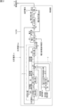
図1は、自立運転する2台のインバータ1,2を、交流電路5に対して並列に接続した、並列インバータシステム100の一例を示す接続図である。なお、各インバータ1,2は、商用電力系統と系統連系して運転することもできるが、本開示では、自立運転時の状態についてのみ示している。2台のインバータとしたのは「複数」の最小限構成例であり、3台以上であってもよい。
Parallel inverter system
1 is a connection diagram showing an example of a
図1において、第1のインバータ1には、直流電圧源3が接続されている。直流電圧源3は、太陽光発電パネル又は蓄電池等の電源そのものであってもよいし、電源にDC/DCコンバータを介した回路であってもよい。同様に、第2のインバータ2には、直流電圧源4が接続されている。第1のインバータ1及び第2のインバータ2は、交流電路5に対して並列に接続されている。交流電路5には負荷(交流負荷)6が接続されている。In FIG. 1, a DC voltage source 3 is connected to a
第1のインバータ1は、制御部1Aと、電力変換部1Bとによって構成される。電力変換部1Bは、直流電圧源3に接続されたフルブリッジ回路10と、フルブリッジ回路10の交流側の2線に設けられた交流リアクトル15と、交流側コンデンサ16と、電圧センサ17と、電流センサ18と、電圧センサ19とを備え、これらは図示のように接続されている。The
フルブリッジ回路10は、スイッチング素子11,12,13,14と、これらにそれぞれ逆並列に接続されたダイオード11d,12d,13d,14dとによって構成されている。図示しているスイッチング素子11,12,13,14は、IGBT(Insulated Gate Bipolar Transistor)であるが、代わりにMOS-FET(Metal-Oxide-Semiconductor Field Effect Transistor)を用いてもよい。The full-
フルブリッジ回路10は、直流電圧源3の両端に接続されている。電圧センサ17は、直流電圧源3からフルブリッジ回路10に入力される直流電圧を検出し、検出出力を制御部1Aに送る。電流センサ18は、交流リアクトル15に流れる電流を検出し、検出出力を制御部1Aに送る。電圧センサ19は、交流電路5に出力される交流電圧を検出し、検出出力を制御部1Aに送る。The
上記のように構成されたインバータ1は、自立運転時に、直流電圧源3から入力された直流電力を、PWM(Pulse Width Modulation)制御されるフルブリッジ回路10により、電圧制御された交流電力に変換する。交流波形に含まれる高周波リプルは交流リアクトル15及び交流側コンデンサ16により抑制される。インバータ1の交流出力は、交流電路5に提供され、負荷6に供給される。During independent operation, the
同様に、第2のインバータ2は、制御部2Aと、電力変換部2Bとによって構成される。電力変換部2Bは、直流電圧源4に接続されたフルブリッジ回路20と、フルブリッジ回路20の交流側の2線に設けられた交流リアクトル25と、交流側コンデンサ26と、電圧センサ27と、電流センサ28と、電圧センサ29とを備え、これらは図示のように接続されている。Similarly, the
フルブリッジ回路20は、スイッチング素子21,22,23,24と、これらにそれぞれ逆並列に接続されたダイオード21d,22d,23d,24dとによって構成されている。The
フルブリッジ回路20は、直流電圧源4の両端に接続されている。電圧センサ27は、直流電圧源4からフルブリッジ回路20に入力される直流電圧を検出し、検出出力を制御部2Aに送る。電流センサ28は、交流リアクトル25に流れる電流を検出し、検出出力を制御部2Aに送る。電圧センサ29は、交流電路5に出力される交流電圧を検出し、検出出力を制御部2Aに送る。The
上記のように構成されたインバータ2は、自立運転時に、直流電圧源4から入力された直流電力を、PWM制御されるフルブリッジ回路20により、電圧制御された交流電力に変換する。交流波形に含まれる高周波リプルは交流リアクトル25及び交流側コンデンサ26により抑制される。インバータ2の交流出力は、交流電路5に提供され、負荷6に供給される。During independent operation, the
第1のインバータ1及び第2のインバータにおける制御部1A,2Aは共に、コンピュータを含み、コンピュータがソフトウェア(コンピュータプログラム)を実行することで、必要な制御機能を実現する。ソフトウェアは、制御部の記憶装置(図示せず。)に格納される。The
《制御部の機能》
次に、制御部1Aの機能(制御部2Aも同様であり、以下、単に「制御部」と言う。)について説明する。
図2は、制御部における電圧制御に関する制御ブロック図である。なお、この図は、説明の簡素化のため、電流制御ループを含まない最もシンプルな例としている。また、図3は、図2の制御ブロック図を、フローチャートとして表現した図である。
<<Function of the control unit>>
Next, the function of the
Fig. 2 is a control block diagram relating to voltage control in the control unit. For the sake of simplicity, this diagram shows the simplest example that does not include a current control loop. Fig. 3 is a diagram expressing the control block diagram of Fig. 2 as a flow chart.
以下、図2と図3とを対応付けて説明する。
まず、図3において、制御部は、位相差検出値Δθを求める(ステップS1)。
図2では、位相差検出器B1に、交流電圧vaと内部位相(前回値)θとが入力され、位相差検出値Δθが得られる。
The following description will be given with reference to FIG. 2 and FIG.
First, in FIG. 3, the control unit obtains a phase difference detection value Δθ (step S1).
In FIG. 2, an AC voltage va and an internal phase (previous value) θ are input to a phase difference detector B1, which obtains a phase difference detection value Δθ.
次に、図3において、制御部は第1の周波数補正値Δf1を求める(ステップS2)。
図2では、位相差検出値Δθが、第1比例積分器B2を経て、周波数補正値Δf1となる。
Next, in FIG. 3, the control unit obtains a first frequency correction value Δf1 (step S2).
In FIG. 2, the phase difference detection value Δθ passes through a first proportional integrator B2 and becomes a frequency correction value Δf1.
次に、図3において、制御部は第2の周波数補正値Δf2を求める(ステップS3)。
図2では、加算器B5において、周波数基準値foと、周波数検出値fの前回値とが比較され、その差が、第2比例積分器B6を経て、周波数補正値Δf2となる。
Next, in FIG. 3, the control unit obtains a second frequency correction value Δf2 (step S3).
In FIG. 2, an adder B5 compares the reference frequency value fo with the previous value of the detected frequency value f, and the difference between them is passed through a second proportional integrator B6 to become a frequency correction value Δf2.
次に、図3において、制御部は、周波数検出値fを求める(ステップS4)。
図2では、周波数補正値Δf1と、周波数補正値Δf2と、周波数基準値foとが相互に加算器B3により加算され、新しい周波数検出値fが得られる。最初に、新しい周波数検出値fを決める際は、前回値の周波数検出値fが用いられる。
Next, in FIG. 3, the control unit obtains a frequency detection value f (step S4).
2, the frequency correction value Δf1, the frequency correction value Δf2, and the frequency reference value fo are added together by an adder B3 to obtain a new frequency detection value f. First, when determining a new frequency detection value f, the previous frequency detection value f is used.
次に、図3において、制御部は、内部位相θを求める(ステップS5)。
図2では、周波数検出値fが積分器B4を経て内部位相θとなる。内部位相θは、位相同期ループLの出力であり、また、この位相同期ループLの中に、ループ内ループとして、周波数フィードバックループFが組み込まれていることになる。
Next, in FIG. 3, the control unit obtains the internal phase θ (step S5).
2, the frequency detection value f passes through an integrator B4 to become an internal phase θ. The internal phase θ is the output of a phase-locked loop L, in which a frequency feedback loop F is incorporated as an inner loop.
次に、図3において、制御部は、電圧指令値va*を求める(ステップS6)。
図2では、内部位相θと、電圧振幅基準値E0とに基づいて、電圧指令部B7が電圧指令値va*を出力する。
Next, in FIG. 3, the control unit obtains a voltage command value va * (step S6).
In FIG. 2, a voltage command unit B7 outputs a voltage command value va * based on an internal phase θ and a voltage amplitude reference value E0.
次に、図3において、制御部は、電圧補正値Δvaを求める(ステップS7)。
図2では、電圧指令値va*と交流電圧vaとが加算器B8により比較され、比例器B9により比例処理を施されて電圧補正値Δvaとなる。なお、電圧補正値Δvaを求める演算には、交流電流iaを用いることもできる。
Next, in FIG. 3, the control unit obtains a voltage correction value Δva (step S7).
2, the voltage command value va * and the AC voltage va are compared by an adder B8, and proportional processing is performed by a proportionality calculator B9 to obtain a voltage correction value Δva. Note that the AC current ia can also be used in the calculation to obtain the voltage correction value Δva.
電圧補正値Δvaの演算に、仮に、比例積分制御を用いると、2台のインバータの交流電圧vaの偏差が大きくなるに従って、2台のインバータの間に流れる横流による無効電力が大きくなる。この結果、出力電流に偏差、直流分、及び、位相差が発生する。しかし、比例制御(比例器B9)とすれば2台のインバータ間で交流電圧vaに偏差が1%程度あっても横流は、ほとんど流れず、2台のインバータの出力は均一になる。If proportional-integral control is used to calculate the voltage correction value Δva, the greater the deviation in the AC voltage va between the two inverters, the greater the reactive power caused by the cross current flowing between the two inverters. This results in a deviation in the output current, a DC component, and a phase difference. However, if proportional control (proportional regulator B9) is used, even if the deviation in the AC voltage va between the two inverters is around 1%, almost no cross current flows, and the output of the two inverters becomes uniform.
そして、図3において、制御部は、インバータの制御信号を求める(ステップS8)。
図2では、電圧指令値va*と電圧補正値Δvaとに基づいてPWM信号生成部B10により、パルス幅変調されたインバータ制御信号が生成され、これに基づいてインバータのゲート駆動信号が得られる。PWM信号生成部B10には、直流電圧viも与えられている。
Then, in FIG. 3, the control unit obtains a control signal for the inverter (step S8).
2, a PWM signal generating unit B10 generates a pulse-width modulated inverter control signal based on the voltage command value va * and the voltage correction value Δva, and a gate drive signal for the inverter is obtained based on this. The PWM signal generating unit B10 is also supplied with a DC voltage vi.
図3のフローチャートに示す処理は、インバータ1,2の自立運転中、繰り返し実行される。
図2において、位相差検出器B1、第1比例積分器B2、加算器B3、及び、積分器B4は、位相同期ループLを形成している。
また、加算器B3、加算器B5、及び、第2比例積分器B6は、周波数フィードバックループFを形成している。自立運転ではなく、系統連系運転を行う場合のインバータは、このような周波数フィードバックループFを使用しなくてもよい。
The process shown in the flowchart of FIG. 3 is repeatedly executed during the independent operation of the
In FIG. 2, a phase-locked loop L is formed by a phase difference detector B1, a first proportional integrator B2, an adder B3, and an integrator B4.
Further, the adder B3, the adder B5, and the second proportional integrator B6 form a frequency feedback loop F. In the case of performing grid-connected operation rather than stand-alone operation, the inverter does not need to use such a frequency feedback loop F.
《検証》
まず、上記のような周波数フィードバックループを使用しない制御の参考例から、シミュレーションにより検証する。
"verification"
First, a reference example of control that does not use a frequency feedback loop as described above will be verified by simulation.
(参考例1)
図4は、系統連系運転を行う場合と同様の制御により、第1,第2の2台のインバータを自立出力で並列運転した場合の、シミュレーション結果である。(a),(b),(c),(d)における横軸は共通であり、時間を表している(0~2秒)。縦軸の数値は、電圧、電流又は周波数を表している。この制御では、第1のインバータを先に運転して、1秒後に第2のインバータの運転を開始している。
(Reference Example 1)
Figure 4 shows the simulation results when two inverters, the first and second inverters, are operated in parallel with independent output under the same control as in the case of grid-connected operation. The horizontal axis in (a), (b), (c), and (d) is the same and represents time (0 to 2 seconds). The values on the vertical axis represent voltage, current, or frequency. In this control, the first inverter is operated first, and the second inverter starts operating one second later.
(a)は、交流電圧vaと、第1のインバータが出力する交流電流とを、重ねて表示した波形図である。振幅が大きい方が交流電圧va、小さい方が交流電流である。
(b)は、dq変換後の2相の電圧vd(上)、vq(下)の波形図である。
(c)は、位相同期ループの出力周波数である。
(d)は、第1のインバータ及び第2のインバータの出力電流である。0~約1.1秒までは、振幅の大きい方が第1のインバータ、振幅の小さい方が第2のインバータである。約1.1秒~約1.5秒では、両者が互いに重なっている。
1A is a waveform diagram showing an AC voltage va and an AC current output from a first inverter, the larger amplitude being the AC voltage va and the smaller amplitude being the AC current.
4B is a waveform diagram of two-phase voltages vd (top) and vq (bottom) after dq transformation.
(c) is the output frequency of the phase locked loop.
(d) shows the output currents of the first inverter and the second inverter. From 0 to about 1.1 seconds, the first inverter has a larger amplitude, and the second inverter has a smaller amplitude. From about 1.1 seconds to about 1.5 seconds, the two inverters overlap each other.
図4の(d)より、第2のインバータの出力開始後すぐに、2台のインバータは出力電流を均等に分担し、横流もほとんど発生しない。しかし、(b)に示すように、電圧vqは0にならず、-20V付近にとどまっている。周波数は、(c)に示すように、初期値から下がり続け、1.5秒を超えると制御不能になった。系統電圧がある場合には、位相同期ループに入力する交流電圧の位相は、位相同期ループの内部周波数によらず一定である。そのため、dq変換で得られる電圧vqを位相比較器として使うことができる。しかし、自立出力では交流電圧の位相が内部周波数によって変化するので、交流電圧を基準位相にすると周波数は収束しない。As shown in (d) of Figure 4, immediately after the second inverter starts outputting, the two inverters share the output current equally and almost no cross current occurs. However, as shown in (b), the voltage vq does not become 0 but remains near -20V. As shown in (c), the frequency continues to drop from the initial value and becomes uncontrollable after 1.5 seconds. When there is a grid voltage, the phase of the AC voltage input to the phase-locked loop is constant regardless of the internal frequency of the phase-locked loop. Therefore, the voltage vq obtained by the dq transformation can be used as a phase comparator. However, in an independent output, the phase of the AC voltage changes depending on the internal frequency, so if the AC voltage is used as the reference phase, the frequency does not converge.
(参考例2)
図5は、周波数を60Hzに固定した基準電圧信号を用いて、第1,第2の2台のインバータを自立出力で並列運転した場合の、シミュレーション結果である。(a),(b),(c),(d)における横軸は共通であり、時間を表している(0~10秒)。縦軸の数値は、電圧、電流又は周波数を表している。右端には、10秒直前の横軸(時間軸)を拡大し、かつ、(c)及び(d)については縦軸も拡大した図を示している。
(Reference Example 2)
Figure 5 shows the simulation results when two inverters, the first and second, are operated in parallel with independent output using a reference voltage signal with a fixed frequency of 60 Hz. The horizontal axis in (a), (b), (c), and (d) is the same and represents time (0 to 10 seconds). The values on the vertical axis represent voltage, current, or frequency. The rightmost figure shows an expanded horizontal axis (time axis) just before 10 seconds, and an expanded vertical axis for (c) and (d).
(a)は、交流電圧vaと、第1のインバータが出力する交流電流とを、重ねて表示した波形図である。振幅が大きい方が交流電圧va、0付近で振動するのが交流電流である。
(b)は、dq変換後の2相の電圧vd(上)、vq(下)の波形図である。
(c)は、位相同期ループの出力周波数である。
(d)は、第1のインバータ及び第2のインバータの出力電流である。第1のインバータより1秒遅れて第2のインバータが運転開始している。
1A is a waveform diagram showing an AC voltage va and an AC current output from the first inverter, superimposed on each other. The AC voltage va has a larger amplitude, and the AC current oscillates near 0.
4B is a waveform diagram of two-phase voltages vd (top) and vq (bottom) after dq transformation.
(c) is the output frequency of the phase locked loop.
(d) shows the output currents of the first inverter and the second inverter. The second inverter starts operating one second after the first inverter.
図5の(b)によれば電圧Vqは0となり、位相同期ループの出力周波数は(c)に示すように、60Hzに収束する。しかし、この制御では、2台のインバータに共通の基準電圧信号を共有するための信号線が必要になる。そのため、信号線へのノイズの影響を受けやすくなる。According to (b) of Figure 5, the voltage Vq becomes 0, and the output frequency of the phase-locked loop converges to 60 Hz as shown in (c). However, this control requires a signal line to share a common reference voltage signal between the two inverters. This makes the signal line susceptible to noise.
(図2の制御ブロック図に基づく制御)
図6は、図2の制御ブロック図に基づく制御を行った場合の、シミュレーション結果である。(a),(b),(c),(d)における横軸は共通であり、時間を表している(0~10秒)。縦軸の数値は、電圧、電流又は周波数を表している。右端には、10秒直前の横軸(時間軸)を拡大し、かつ、(c)及び(d)については縦軸も拡大した図を示している。周波数フィードバックループFにおける第2比例積分器B6の比例ゲインを0.2、積分時定数を0.01秒とした。
(Control based on the control block diagram of FIG. 2)
Figure 6 shows the simulation results when control is performed based on the control block diagram of Figure 2. The horizontal axis in (a), (b), (c), and (d) is the same and represents time (0 to 10 seconds). The values on the vertical axis represent voltage, current, or frequency. The rightmost diagram shows an enlarged view of the horizontal axis (time axis) just before 10 seconds, and the vertical axis in (c) and (d) is also enlarged. The proportional gain of the second proportional integrator B6 in the frequency feedback loop F was set to 0.2, and the integral time constant was set to 0.01 seconds.
(a)は、交流電圧vaと、第1のインバータが出力する交流電流とを、重ねて表示した波形図である。振幅が大きい方が交流電圧va、0付近で振動するのが交流電流である。
(b)は、dq変換後の2相の電圧vd(上)、vq(下)の波形図である。
(c)は、位相同期ループの出力周波数である。
(d)は、第1のインバータ及び第2のインバータの出力電流である。第1のインバータより1秒遅れて第2のインバータが運転開始している。
1A is a waveform diagram showing an AC voltage va and an AC current output from the first inverter, superimposed on each other. The AC voltage va has a larger amplitude, and the AC current oscillates near 0.
4B is a waveform diagram of two-phase voltages vd (top) and vq (bottom) after dq transformation.
(c) is the output frequency of the phase locked loop.
(d) shows the output currents of the first inverter and the second inverter. The second inverter starts operating one second after the first inverter.
図6によれば、(b)に示すように、電圧vqは0にはならないが、負の一定値に収束する。位相同期ループLの周波数は、(c)に示すように、概ね目標どおりの一定値に収束する。また、(d)に示すように、第2のインバータが運転開始してからの出力電流は2台で均等に分担され、力率1で、直流分も発生していない。制御不能となるような事態は発生せず、周波数は安定している。このように、位相同期ループLの周波数制御に、周波数フィードバックループFを取り入れたことで、自立出力を交流電路に提供するインバータの並列運転を安定させることができる。 According to FIG. 6, as shown in (b), the voltage vq does not become 0, but converges to a constant negative value. As shown in (c), the frequency of the phase-locked loop L converges to a constant value roughly as targeted. Also, as shown in (d), the output current after the second inverter starts operating is shared equally between the two inverters, the power factor is 1, and no DC component is generated. No uncontrollable situation occurs, and the frequency is stable. In this way, by incorporating a frequency feedback loop F into the frequency control of the phase-locked loop L, it is possible to stabilize the parallel operation of inverters that provide independent outputs to AC circuits.
《発電機との並列運転》
図8の(a)は、図2に示す周波数フィードバック付きの位相同期ループを有するインバータの、並列運転を行った場合において、インバータ(電力変換部)の出力電流Iと、内部位相差φとの関係の一例を示すグラフである。位相差φは出力電流Iと比例的な関係にあり、出力電流Iが増大すれば、位相差φも増大する。これは、同期発電機の出力電流と内部位相角との関係と同様である。
<Parallel operation with a generator>
Fig. 8(a) is a graph showing an example of the relationship between the output current I and the internal phase difference φ of the inverter (power conversion unit) when the inverters having the phase-locked loop with frequency feedback shown in Fig. 2 are operated in parallel. The phase difference φ is proportional to the output current I, and as the output current I increases, the phase difference φ also increases. This is similar to the relationship between the output current and the internal phase angle of a synchronous generator.
図8の(b)は、等価的な誘導起電力Eと、位相差φと、交流電圧Vとの関係を示すベクトル図である。ここで、インバータを、同期リアクタンスxsの同期発電機と考えると、位相差φは、sinφ≒φとすれば、以下の関係となる。
φ≒(jxsI)/E
すなわち、位相同期ループに周波数フィードバック処理を付加したインバータは、一種の仮想同期発電機(VSG:Vertual Synchronous Generator)として動作する。従って、当該インバータは、同期発電機との並列運転も可能である。
8B is a vector diagram showing the relationship between the equivalent induced electromotive force E, the phase difference φ, and the AC voltage V. If the inverter is considered as a synchronous generator with synchronous reactance xs , and the phase difference φ is sinφ≈φ, then the following relationship holds:
φ≒(jx s I)/E
That is, an inverter in which frequency feedback processing is added to a phase locked loop operates as a kind of virtual synchronous generator (VSG). Therefore, the inverter can be operated in parallel with a synchronous generator.
図7は、図1の並列インバータシステム100と、商用電力系統の発電機とを並列運転した場合の、シミュレーション結果である。(a),(b),(c),(d)における横軸は共通であり、時間を表している(9.9~10.1秒)。縦軸の数値は、電圧、電流又は周波数を表している。
Figure 7 shows the simulation results when the
図7の(a)は、交流電圧vaと、第1のインバータが出力する交流電流とを、重ねて表示した波形図である。振幅が大きい方が交流電圧va、0付近で振動するのが交流電流である。
(b)は、dq変換後の2相の電圧vd(上)、vq(下)の波形図である。
(c)は、位相同期ループの出力周波数である。
(d)は、第1のインバータ及び第2のインバータの出力電流である。時刻10秒で発電機を解列している。
7A is a waveform diagram showing the AC voltage va and the AC current output by the first inverter, superimposed on each other. The AC voltage va has a larger amplitude, and the AC current oscillates near 0.
4B is a waveform diagram of two-phase voltages vd (top) and vq (bottom) after dq transformation.
(c) is the output frequency of the phase locked loop.
(d) is the output current of the first inverter and the second inverter. The generator is disconnected at
図7に示すように、2台のインバータと発電機とを互いに並列接続した場合にも、並列運転は可能であり、2台のインバータの出力電流は一致した。但し、出力電流には実効値の50%強の直流分が含まれており、力率は0.824に低下する。負荷には直流分は流れておらず、インバータが出力する直流電流成分を交流電源が吸収している。 As shown in Figure 7, parallel operation is possible even when two inverters and generators are connected in parallel with each other, and the output currents of the two inverters are the same. However, the output current contains a DC component that is just over 50% of the effective value, and the power factor drops to 0.824. No DC component flows through the load, and the DC current component output by the inverter is absorbed by the AC power supply.
電流指令値の演算には、直流分抑制のためのハイパスフィルタ、及び、発振抑制のためのローパスフィルタを設ける。その結果として、直流分は低減され、力率は0.993に改善される。10秒経過後に発電機を解列すると、交流電圧vaは、ほとんど変化せず、2台のインバータの出力電流が増えて、発電機が負担していた電流を補った。解列後は電圧vq及び位相同期ループの出力周波数が僅かに低下したが、2台のインバータが負荷電流20Aの半分をそれぞれ均等に負担している。 A high-pass filter to suppress the DC component and a low-pass filter to suppress oscillation are provided in the calculation of the current command value. As a result, the DC component is reduced and the power factor is improved to 0.993. When the generator is disconnected after 10 seconds, the AC voltage va barely changes, and the output current of the two inverters increases, compensating for the current that the generator had been carrying. After disconnection, the voltage vq and the output frequency of the phase-locked loop drop slightly, but the two inverters each bear half of the load current of 20A equally.
2台のインバータが負担する電流の割合を制御するには、インバータの出力に応じて、制御目標値を変化させればよい。電圧位相を進めれば有効電力が増え、電圧振幅を大きくすれば無効電力が増えるので、最も単純な方法としては、例えば電圧指令値v*を、
v*=E*cos2πf*t
とすると、無効電力の増大に応じて電圧振幅目標値E*が低下し、また、有効電力の増大に応じて周波数目標値f*が低下する垂下特性を付与することが考えられる。
To control the ratio of the current shared by the two inverters, the control target value can be changed according to the inverter output. If the voltage phase is advanced, the active power increases, and if the voltage amplitude is increased, the reactive power increases. Therefore, the simplest method is to set the voltage command value v * as follows:
v * = E * cos2πf * t
In this case, it is possible to provide a drooping characteristic in which the voltage amplitude target value E * decreases in response to an increase in reactive power, and the frequency target value f * decreases in response to an increase in active power.
位相同期ループの出力位相は、同期発電機と同様に交流電圧よりも進み、位相差はインバータの出力電流に比例して増加する。このような位相同期ループで制御した自立出力のインバータは、複数台を並列運転するだけでなく、他の交流電源との並列運転も行うことができ、仮想同期発電機として扱うことができる。 The output phase of the phase-locked loop leads the AC voltage, just like a synchronous generator, and the phase difference increases in proportion to the inverter's output current. Inverters with independent output controlled by such a phase-locked loop can be operated not only in parallel in multiple units, but also in parallel with other AC power sources, and can be treated as virtual synchronous generators.
《まとめ》
以上の開示は、一般化して以下のように表現することができる。
図1に示した第1のインバータ(1)及び第2のインバータ(2)の各々における制御部は、交流電圧(Va)に基づいて実行する位相同期ループ(L)において周波数検出値を算出する演算に、当該周波数検出値の前回値と周波数基準値との比較結果に比例積分を施して得た周波数補正値(Δf2)を加える周波数フィードバック処理(周波数フィードバックループ(F))を付加している。
このようなインバータは、自立出力の周波数が目標値に漸近して収束する。従って、かかるインバータを複数台並列に接続した場合、または、他の交流電源と並列接続した場合に、安定した並列運転を行うことができる。
"summary"
The above disclosure can be generalized and expressed as follows.
The control unit in each of the first inverter (1) and the second inverter (2) shown in FIG. 1 adds a frequency feedback process (frequency feedback loop (F)) to a calculation for calculating a frequency detection value in a phase-locked loop (L) executed based on an AC voltage (Va), in which a frequency correction value (Δf2) obtained by applying proportional integration to a comparison result between a previous value of the frequency detection value and a frequency reference value is added.
In such an inverter, the frequency of the independent output asymptotically converges to a target value, and therefore, when multiple such inverters are connected in parallel or when connected in parallel to another AC power source, stable parallel operation can be achieved.
より具体的には、前記周波数補正値(Δf2)を第2の周波数補正値とすると、制御部は、電圧センサ(19,29)の検出出力に基づく電圧位相と位相同期ループ(L)内の内部位相との偏差に基づいて、第1の周波数補正値(Δf1)を求める第1演算と、周波数基準値(fo)に、第1の周波数補正値(Δf1)及び第2の周波数補正値(Δf2)を加算して新たな周波数検出値(f)を求める第2演算と、新たな周波数検出値(f)に基づいて、新たな周波数検出値に基づいて電力変換部(1B,2B)の出力を制御する制御する制御信号を生成する第3演算と、を実行する。
上記の第2演算を行うことにより、自立出力の周波数が収束しない状態に陥るのを抑制することができる。
More specifically, when the frequency correction value (Δf2) is defined as a second frequency correction value, the control unit executes a first calculation to obtain a first frequency correction value (Δf1) based on the deviation between the voltage phase based on the detection output of the voltage sensor (19, 29) and the internal phase in the phase-locked loop (L), a second calculation to obtain a new frequency detection value (f) by adding the first frequency correction value (Δf1) and the second frequency correction value (Δf2) to the frequency reference value (fo), and a third calculation to generate a control signal for controlling the output of the power conversion unit (1B, 2B) based on the new frequency detection value (f).
By performing the above-described second calculation, it is possible to prevent the frequency of the independent output from falling into a state where it does not converge.
また、第3演算には、新たな周波数検出値(f)に基づいて電圧指令値(va*)を求めること、及び、電圧指令値(va*)と、交流電圧との偏差に、比例演算を施して電圧補正値(Δva)を求めること、が含まれる。
この場合、比例積分演算ではなく比例演算を行うことにより、他の交流電源との間で、交流電圧として検出した値に差があっても、横流を抑制することができる。
The third calculation also includes determining a voltage command value (va * ) based on the new frequency detection value (f), and determining a voltage correction value (Δva) by applying a proportional calculation to the deviation between the voltage command value (va * ) and the AC voltage.
In this case, by performing proportional calculation instead of proportional-integral calculation, cross current can be suppressed even if there is a difference in the value detected as the AC voltage between the other AC power source.
《順変換(充電)について補足》
図1のインバータ1,2は、自立出力のインバータとして説明したが、直流電圧源が蓄電池に基づく場合は、インバータ1,2(電力変換部1B,2B)は、交流電力から直流電力への変換を行うようにしてもよい。例えば、交流電路5に、太陽光発電を電源とする系統連系型のインバータのように、交流電路5の電圧に同期する電流を出力する交流電源(電流源)が接続された場合を考える。この場合、制御部1A,2Aは、交流電源の交流電力を直流電力に変換して電力変換部1B,2Bの直流側に接続される蓄電池を充電するよう制御する。負荷6での消費電力の余剰電力を、インバータ1,2が順変換(交流→直流)して直流電圧源3,4に含まれる蓄電池を充電することができる。なお。この場合は、インバータの位相同期ループにおける内部位相は、交流電圧の位相より遅れる。
<Additional information about forward conversion (charging)>
The
《その他》
なお、図1のフルブリッジ回路10,20は、2レグの単相インバータ回路であるが、3レグの三相インバータ回路であっても、同様に、図2、図3の処理を適用することができる。
"others"
Although the full-
《補記》
なお、今回開示された実施の形態はすべての点で例示であって制限的なものではないと考えられるべきである。本発明の範囲は請求の範囲によって示され、請求の範囲と均等の意味及び範囲内での全ての変更が含まれることが意図される。
《Addendum》
The embodiments disclosed herein should be considered to be illustrative and not restrictive in all respects. The scope of the present invention is defined by the claims, and it is intended to include all modifications within the scope and meaning equivalent to the claims.
1 第1のインバータ
1A 制御部
1B 電力変換部
2 第2のインバータ
2A 制御部
2B 電力変換部
3,4 直流電圧源
5 交流電路
6 負荷
10 フルブリッジ回路
11,12,13,14 スイッチング素子
11d,12d,13d,14d ダイオード
15 交流リアクトル
16交流側コンデンサ
17 電圧センサ
18 電流センサ
19 電圧センサ
20 フルブリッジ回路
21,22,23,24 スイッチング素子
21d,22d,23d,24d ダイオード
25 交流リアクトル
26交流側コンデンサ
27 電圧センサ
28 電流センサ
29 電圧センサ
100 並列インバータシステム
B1 位相差検出器
B2 第1比例積分器
B3 加算器
B4 積分器
B5 加算器
B6 第2比例積分器
B7 電圧指令部
B8 加算器
B9 比例器
B10 PWM信号生成部
F 周波数フィードバックループ
L 位相同期ループ
LIST OF
Claims (7)
直流電力を交流電力に変換して前記交流電路に電力を供給する電力変換部と、
前記交流電路の交流電圧を検出する電圧センサと、
前記電力変換部を制御する制御部と、を備え、
前記制御部は、前記交流電圧に基づいて実行する位相同期ループにおいて周波数検出値を算出する演算に、当該周波数検出値の前回値と周波数基準値との比較結果に比例積分を施して得た周波数補正値を加える周波数フィードバック処理を付加する、インバータ。 An inverter that is connected in parallel to an AC circuit to which an AC power source is connected and provides an independent output,
a power conversion unit that converts DC power into AC power and supplies the power to the AC circuit;
a voltage sensor for detecting an AC voltage of the AC current path;
A control unit that controls the power conversion unit,
The control unit adds a frequency feedback process to a calculation for calculating a frequency detection value in a phase-locked loop executed based on the AC voltage, the frequency correction value being obtained by applying proportional integration to a comparison result between the previous value of the frequency detection value and a frequency reference value.
前記電圧センサの検出出力に基づく電圧位相と前記位相同期ループ内の内部位相との偏差に基づいて、第1の周波数補正値を求める第1演算と、
前記周波数基準値に、前記第1の周波数補正値及び前記第2の周波数補正値を加算して新たな周波数検出値を求める第2演算と、
前記新たな周波数検出値に基づいて前記電力変換部の出力を制御する制御信号を生成する第3演算と、
を実行する請求項1に記載のインバータ。 When the frequency correction value is a second frequency correction value, the control unit
a first calculation for determining a first frequency correction value based on a deviation between a voltage phase based on a detection output of the voltage sensor and an internal phase in the phase locked loop;
a second calculation of adding the first frequency correction value and the second frequency correction value to the frequency reference value to obtain a new frequency detection value;
a third calculation for generating a control signal for controlling an output of the power conversion unit based on the new frequency detection value;
2. The inverter according to claim 1, wherein the inverter performs
前記新たな周波数検出値に基づいて電圧指令値を求めること、及び、
前記電圧指令値と、前記交流電圧との偏差に、比例演算を施して電圧補正値を求めること、
が含まれる請求項2に記載のインバータ。 The third calculation includes:
determining a voltage command value based on the new frequency detection value; and
determining a voltage correction value by performing a proportional operation on the deviation between the voltage command value and the AC voltage;
3. The inverter of claim 2 including:
前記制御部は、前記交流電源の交流電力を直流電力に変換して前記電力変換部の直流側に接続される直流電圧源を充電するよう、前記電力変換部を制御する請求項1から請求項4のいずれか1項に記載のインバータ。 The power conversion unit is also capable of converting AC power to DC power,
5. The inverter according to claim 1, wherein the control unit controls the power conversion unit to convert AC power from the AC power source into DC power and charge a DC voltage source connected to a DC side of the power conversion unit.
前記第1インバータと並列に前記交流電路に接続され、前記交流電路に自立出力を提供する第2インバータと、を備えた並列インバータシステムであって、
前記第1インバータ及び前記第2インバータの各々は、
直流電力を交流電力に変換して前記交流電路に電力を供給する電力変換部と、
前記交流電路の交流電圧を検出する電圧センサと、
前記電力変換部を制御する制御部と、を備え、
前記制御部は、前記交流電圧に基づいて実行する位相同期ループにおいて周波数検出値を算出する演算に、当該周波数検出値の前回値と周波数基準値との比較結果に比例積分を施して得た周波数補正値を加える周波数フィードバック処理を付加する、並列インバータシステム。 a first inverter for providing an isolated output to the AC power line;
A parallel inverter system including: a second inverter connected in parallel with the first inverter to the AC line and providing an independent output to the AC line;
Each of the first inverter and the second inverter has
a power conversion unit that converts DC power into AC power and supplies the power to the AC circuit;
a voltage sensor for detecting an AC voltage of the AC current path;
A control unit that controls the power conversion unit,
The control unit adds a frequency feedback process to a calculation for calculating a frequency detection value in a phase-locked loop executed based on the AC voltage, the frequency correction value being obtained by applying proportional integration to a comparison result between a previous value of the frequency detection value and a frequency reference value.
電力変換部により、直流電力を交流電力に変換して前記交流電路に電力を供給し、
前記電力変換部を制御する制御部は、前記交流電路の交流電圧に基づいて実行する位相同期ループにおいて周波数検出値を算出する演算に、当該周波数検出値の前回値と周波数基準値との比較結果に比例積分を施して得た周波数補正値を加える周波数フィードバック処理を付加する、
インバータの制御方法。
A method for controlling an inverter that is connected in parallel to an AC circuit to which an AC power source is connected and provides an independent output, comprising the steps of:
A power conversion unit converts DC power into AC power and supplies the power to the AC circuit;
The control unit that controls the power conversion unit adds a frequency feedback process to a calculation of a frequency detection value in a phase-locked loop that is executed based on the AC voltage of the AC power line, the frequency correction value being obtained by applying proportional integral to a comparison result between a previous value of the frequency detection value and a frequency reference value.
Inverter control method.
Applications Claiming Priority (3)
| Application Number | Priority Date | Filing Date | Title |
|---|---|---|---|
| JP2021033734 | 2021-03-03 | ||
| JP2021033734 | 2021-03-03 | ||
| PCT/JP2021/040360 WO2022185614A1 (en) | 2021-03-03 | 2021-11-02 | Inverter, parallel inverter system, and method for controlling inverter |
Publications (2)
| Publication Number | Publication Date |
|---|---|
| JPWO2022185614A1 JPWO2022185614A1 (en) | 2022-09-09 |
| JP7613552B2 true JP7613552B2 (en) | 2025-01-15 |
Family
ID=83154244
Family Applications (1)
| Application Number | Title | Priority Date | Filing Date |
|---|---|---|---|
| JP2023503375A Active JP7613552B2 (en) | 2021-03-03 | 2021-11-02 | Inverter, parallel inverter system, and inverter control method |
Country Status (3)
| Country | Link |
|---|---|
| US (1) | US12463554B2 (en) |
| JP (1) | JP7613552B2 (en) |
| WO (1) | WO2022185614A1 (en) |
Families Citing this family (2)
| Publication number | Priority date | Publication date | Assignee | Title |
|---|---|---|---|---|
| US12199441B2 (en) | 2022-02-18 | 2025-01-14 | The University Of North Carolina At Charlotte | Apparatus and method for controlling one or more inverters |
| EP4555616A1 (en) * | 2022-07-11 | 2025-05-21 | Nextracker LLC | Parallel inverter systems and methods |
Citations (3)
| Publication number | Priority date | Publication date | Assignee | Title |
|---|---|---|---|---|
| JP2010161901A (en) | 2009-01-09 | 2010-07-22 | Daihen Corp | Inverter control circuit and grid-connected inverter system with this inverter control circuit |
| JP2015100224A (en) | 2013-11-20 | 2015-05-28 | 株式会社ダイヘン | Control circuit for controlling inverter circuit, inverter device including the control circuit, power system including the inverter device, and control method |
| JP2017225214A (en) | 2016-06-13 | 2017-12-21 | 新電元工業株式会社 | Parallel operation control method and parallel operation control device for three-phase inverter |
Family Cites Families (5)
| Publication number | Priority date | Publication date | Assignee | Title |
|---|---|---|---|---|
| JP4396926B2 (en) | 2004-02-12 | 2010-01-13 | 東芝三菱電機産業システム株式会社 | Power converter |
| US9450513B2 (en) | 2013-09-27 | 2016-09-20 | Daihen Corporation | Control circuit and control method for inverter circuit, and control circuit and control method for power conversion circuit |
| WO2017126205A1 (en) * | 2016-01-20 | 2017-07-27 | 三菱電機株式会社 | Electric power conversion device and electric power conversion system |
| FI3869682T3 (en) * | 2020-02-24 | 2024-07-10 | Danfoss As | METHOD AND CONTROL DEVICE FOR ADJUSTING A POWER CONVERTER |
| JP7387497B2 (en) * | 2020-03-11 | 2023-11-28 | 株式会社東芝 | power converter |
-
2021
- 2021-11-02 WO PCT/JP2021/040360 patent/WO2022185614A1/en not_active Ceased
- 2021-11-02 JP JP2023503375A patent/JP7613552B2/en active Active
- 2021-11-02 US US18/278,410 patent/US12463554B2/en active Active
Patent Citations (3)
| Publication number | Priority date | Publication date | Assignee | Title |
|---|---|---|---|---|
| JP2010161901A (en) | 2009-01-09 | 2010-07-22 | Daihen Corp | Inverter control circuit and grid-connected inverter system with this inverter control circuit |
| JP2015100224A (en) | 2013-11-20 | 2015-05-28 | 株式会社ダイヘン | Control circuit for controlling inverter circuit, inverter device including the control circuit, power system including the inverter device, and control method |
| JP2017225214A (en) | 2016-06-13 | 2017-12-21 | 新電元工業株式会社 | Parallel operation control method and parallel operation control device for three-phase inverter |
Also Published As
| Publication number | Publication date |
|---|---|
| US20240235421A9 (en) | 2024-07-11 |
| WO2022185614A1 (en) | 2022-09-09 |
| JPWO2022185614A1 (en) | 2022-09-09 |
| US20240136947A1 (en) | 2024-04-25 |
| US12463554B2 (en) | 2025-11-04 |
Similar Documents
| Publication | Publication Date | Title |
|---|---|---|
| US8848406B2 (en) | Single-phase voltage type AC/DC converter, three-phase voltage type AC/DC converter, and stabilization control method | |
| CN102299659B (en) | For system and the method for the control of multiphase power converter | |
| US20130181654A1 (en) | Motor drive system employing an active rectifier | |
| JP6744477B2 (en) | Uninterruptible power supply and test method for uninterruptible power supply | |
| US20050195624A1 (en) | Method and arrangement in connection with network inverter | |
| JP7613552B2 (en) | Inverter, parallel inverter system, and inverter control method | |
| JPH0336930A (en) | Three-phase converter | |
| JP2018129963A (en) | Controller of power converter | |
| JP4717114B2 (en) | Control device for power converter | |
| JP2012005202A (en) | Three-phase power converter | |
| JPWO2020105133A1 (en) | Power converter | |
| JP7136368B2 (en) | power converter | |
| JP5833524B2 (en) | Power converter and control device for power converter | |
| JP2017153277A (en) | Self-excited reactive power compensation apparatus | |
| Shin et al. | Active power control for minimum switching of three-phase electrolytic capacitor-less PWM converter | |
| Busquets-Monge et al. | Closed-loop control design for a three-level three-phase neutral-point-clamped inverter using the optimized nearest-three virtual-space-vector modulation | |
| WO2014050935A1 (en) | Single-phase voltage type ac-dc conversion device | |
| JP5616412B2 (en) | Single-phase voltage type AC / DC converter | |
| JP2014135878A (en) | Controller of three-phase converter and electric power conversion system using the same | |
| JP2023050505A (en) | power converter | |
| JP2025031393A (en) | Water electrolysis cell system and method for controlling the water electrolysis cell system | |
| JP2024022201A (en) | Inverter device and motor drive device | |
| Pany | Design considerations of Traction converter for three phase AC locomotive | |
| JP2014072983A (en) | Single-phase voltage type ac-dc conversion device | |
| JPH0720370B2 (en) | Power converter control circuit |
Legal Events
| Date | Code | Title | Description |
|---|---|---|---|
| A621 | Written request for application examination |
Free format text: JAPANESE INTERMEDIATE CODE: A621 Effective date: 20240422 |
|
| TRDD | Decision of grant or rejection written | ||
| A01 | Written decision to grant a patent or to grant a registration (utility model) |
Free format text: JAPANESE INTERMEDIATE CODE: A01 Effective date: 20241126 |
|
| A61 | First payment of annual fees (during grant procedure) |
Free format text: JAPANESE INTERMEDIATE CODE: A61 Effective date: 20241209 |
|
| R150 | Certificate of patent or registration of utility model |
Ref document number: 7613552 Country of ref document: JP Free format text: JAPANESE INTERMEDIATE CODE: R150 |