JP7608865B2 - System equipped with electromagnetic wave absorber and method for absorbing electromagnetic waves using electromagnetic wave absorber - Google Patents
System equipped with electromagnetic wave absorber and method for absorbing electromagnetic waves using electromagnetic wave absorber Download PDFInfo
- Publication number
- JP7608865B2 JP7608865B2 JP2021028922A JP2021028922A JP7608865B2 JP 7608865 B2 JP7608865 B2 JP 7608865B2 JP 2021028922 A JP2021028922 A JP 2021028922A JP 2021028922 A JP2021028922 A JP 2021028922A JP 7608865 B2 JP7608865 B2 JP 7608865B2
- Authority
- JP
- Japan
- Prior art keywords
- electromagnetic wave
- dielectric
- wave absorber
- frequency
- electromagnetic
- Prior art date
- Legal status (The legal status is an assumption and is not a legal conclusion. Google has not performed a legal analysis and makes no representation as to the accuracy of the status listed.)
- Active
Links
Images


Classifications
-
- H—ELECTRICITY
- H01—ELECTRIC ELEMENTS
- H01Q—ANTENNAS, i.e. RADIO AERIALS
- H01Q17/00—Devices for absorbing waves radiated from an antenna; Combinations of such devices with active antenna elements or systems
-
- H—ELECTRICITY
- H05—ELECTRIC TECHNIQUES NOT OTHERWISE PROVIDED FOR
- H05K—PRINTED CIRCUITS; CASINGS OR CONSTRUCTIONAL DETAILS OF ELECTRIC APPARATUS; MANUFACTURE OF ASSEMBLAGES OF ELECTRICAL COMPONENTS
- H05K9/00—Screening of apparatus or components against electric or magnetic fields
Landscapes
- Engineering & Computer Science (AREA)
- Microelectronics & Electronic Packaging (AREA)
- Shielding Devices Or Components To Electric Or Magnetic Fields (AREA)
- Aerials With Secondary Devices (AREA)
Description
本発明は、電磁波吸収体を備えたシステム、及び電磁波吸収体を用いた電磁波の吸収方法に関する。 The present invention relates to a system equipped with an electromagnetic wave absorber and a method for absorbing electromagnetic waves using an electromagnetic wave absorber.
メタマテリアルは、そのサイズが対象とする電磁波の波長に比べて小さい人工物質であり、自然界の物質には無い特性を示すことから、近年、注目を浴びている。特に、左手系メタマテリアルと呼ばれる物質は、特定の周波数領域で負の屈折率を示す。そのため、完全レンズや透明マントといった新規な光学用途での応用を目指して、研究開発が盛んにおこなわれている。 Metamaterials are artificial materials whose size is smaller than the wavelength of the electromagnetic waves they target, and have attracted attention in recent years because they exhibit properties not found in natural materials. In particular, materials known as left-handed metamaterials exhibit a negative refractive index in a specific frequency range. For this reason, research and development is being actively conducted with the aim of applying them to new optical applications such as perfect lenses and invisibility cloaks.
1999年に英国の物理学者J.B.Pendryは、電磁波の波長に比べて小さい周期構造を有するナノメタル構造体を提案し、この構造体の屈折率が負になることを理論的に示した(非特許文献1)。このナノメタル構造体は、微小なスプリットリング共振器(SRR)とメタルワイヤからなるナノユニットを3次元的に配列した構造を備えている。ナノユニットのサイズを小さくすることで、ナノメタル構造体は電磁波に対して均質な媒質として働き、SRRとメタルワイヤの機能に依存する電磁波応答を示す。SRRは電磁波に対してLC共振器として働き、共振周波数の上側で負の透磁率を示す。また導電性メタルワイヤは負の誘電率を示す。SRRとメタルワイヤを組み合わせることで、実効誘電率と実効透磁率の両方が負になり、その結果、誘電率の平方根と透磁率の平方根との積で表される屈折率が負になる。さらにPendryは、負の屈折率を示す左手系メタマテリアルを用いることで、光の回折限界を超えて、いくらでも細かな構造を観察できる完全レンズが実現できることを理論的に示した(非特許文献2)。 In 1999, British physicist J. B. Pendry proposed a nanometal structure with a periodic structure smaller than the wavelength of electromagnetic waves, and theoretically demonstrated that the refractive index of this structure is negative (Non-Patent Document 1). This nanometal structure has a structure in which nanounits consisting of tiny split ring resonators (SRRs) and metal wires are arranged three-dimensionally. By reducing the size of the nanounits, the nanometal structure acts as a homogeneous medium for electromagnetic waves and exhibits electromagnetic wave response that depends on the functions of the SRRs and metal wires. The SRRs act as LC resonators for electromagnetic waves and exhibit negative permeability above the resonant frequency. In addition, conductive metal wires exhibit negative dielectric constants. By combining the SRRs and metal wires, both the effective dielectric constant and the effective permeability become negative, and as a result, the refractive index, which is expressed as the product of the square root of the dielectric constant and the square root of the permeability, becomes negative. Furthermore, Pendry theoretically demonstrated that by using a left-handed metamaterial that exhibits a negative refractive index, it is possible to realize a perfect lens that goes beyond the diffraction limit of light and allows the observation of infinitesimally fine structures (Non-Patent Document 2).
Pendryの発表を受けて、米国の物理学者D.R.Smithらは、SRRとメタルワイヤからなるナノメタル構造体を実際に作製し、この構造物の誘電率と透磁率とがマイクロ波領域で負になることを実証した(非特許文献3)。これらの発表を受けて、メタマテリアルは一気に注目を浴びるようになった。 Following Pendry's announcement, American physicist D. R. Smith and his colleagues actually created a nanometal structure consisting of SRRs and metal wires, and demonstrated that the dielectric constant and permeability of this structure are negative in the microwave region (Non-Patent Document 3). Following these announcements, metamaterials suddenly began to attract attention.
一方で、ナノメタル構造体の代わりに誘電体を用いた誘電体メタマテリアルが提案されている。ナノメタル構造物は、導体損が大きく、また製造のために精密微細な加工技術が必要との欠点がある。これに対して、誘電体メタマテリアルは、非共振時の損失が小さく、製造が容易という利点がある。 On the other hand, dielectric metamaterials have been proposed, which use dielectrics instead of nanometal structures. Nanometal structures have the disadvantages of large conductor loss and the need for precise and fine processing techniques for manufacturing. In contrast, dielectric metamaterials have the advantages of small loss when not resonating and being easy to manufacture.
例えば、R.Yahiaouiらは、高誘電率TiO2セラミックディスクからなる誘電体共振器を2次元的に周期配列した構造を提案している(非特許文献4)。誘電体共振器のサイズを電磁波の波長程度に小さくすると、Mie共鳴が起こる。そのためTE共振とTM共振のいずれの共振モードを利用することが可能になる。誘電体共振器は、TE共振モードにおいて共振周波数の上側で負の実効透磁率を示す。またTM共振モードにおいて共振周波数の上側で負の実効誘電率を示す。この点、TE共振モードが、ナノメタル構造のSRRに相当し、TM共振モードがメタルワイヤに相当すると言うことができる。 For example, R. Yahiaoui et al. have proposed a structure in which dielectric resonators made of high dielectric constant TiO2 ceramic disks are arranged periodically in a two-dimensional manner (Non-Patent Document 4). When the size of the dielectric resonator is reduced to about the wavelength of the electromagnetic wave, Mie resonance occurs. Therefore, it becomes possible to use either the TE resonance or the TM resonance mode. In the TE resonance mode, the dielectric resonator shows a negative effective permeability above the resonance frequency. Also, in the TM resonance mode, the dielectric resonator shows a negative effective permittivity above the resonance frequency. In this respect, it can be said that the TE resonance mode corresponds to the SRR of the nanometal structure, and the TM resonance mode corresponds to the metal wire.
このように、誘電体メタマテリアルなどのメタマテリアルに関する開発が盛んに行われるものの、その殆どが、負の屈折率を示す物質、即ち左手系メタマテリアルを対象とし、また完全レンズや透明マントといった光学用途での応用を目指している。ナノメタル構造体を、マイクロ波領域におけるアンテナや伝送線路に適用する技術が僅かに知られるものの、誘電体メタマテリアルを光学部品以外の電子デバイスに適用することを目指した技術は知られていない。 Though there has been active development of metamaterials such as dielectric metamaterials, most of this research focuses on materials that exhibit a negative refractive index, i.e., left-handed metamaterials, and aims for optical applications such as perfect lenses and transparency cloaks. Although there are a few known technologies for applying nanometal structures to antennas and transmission lines in the microwave region, there is no known technology aimed at applying dielectric metamaterials to electronic devices other than optical components.
一方で、近年の電子情報通信技術の急速な発展に伴い、電磁波の利用が急速に増えるとともに、使用される電磁波の高周波化及び広帯域化が進んでいる。また電磁波の利用拡大及び高周波化が進むにつれて、電磁ノイズによる電子機器の誤作動や身体への悪影響といった電磁干渉の問題がクローズアップされ、EMC対策への要望が高まっている。 On the other hand, with the rapid development of electronic, information and communication technology in recent years, the use of electromagnetic waves has increased rapidly, and the electromagnetic waves used are becoming higher in frequency and wider in bandwidth. Furthermore, as the use of electromagnetic waves expands and becomes more frequent, issues of electromagnetic interference, such as malfunctions of electronic devices and adverse effects on the body due to electromagnetic noise, have come into focus, and there is a growing demand for EMC measures.
EMC対策の一手段として、電磁波吸収体(電波吸収体)を用いて不要な電磁波を吸収し、その侵入を防ぐ手法が提案されている。電磁波吸収体は、入射した電磁波のエネルギー(電磁波エネルギー)を吸収体が吸収し、これを熱エネルギーに変換して放射する現象(吸収減衰)を利用する。吸収減衰を効果的に利用するためには、優れた吸収特性を示す吸収体(吸収材料)を用いることが重要である。具体的には、吸収体の伝送減衰量(率)が吸収帯域において高いことが望まれる。 As one method of EMC countermeasures, a method has been proposed in which electromagnetic wave absorbers (radio wave absorbers) are used to absorb unnecessary electromagnetic waves and prevent their intrusion. Electromagnetic wave absorbers utilize the phenomenon (absorption attenuation) in which the absorber absorbs the energy of incident electromagnetic waves (electromagnetic wave energy), converts it to thermal energy, and radiates it. To effectively utilize absorption attenuation, it is important to use an absorber (absorption material) that exhibits excellent absorption characteristics. Specifically, it is desirable for the absorber's transmission attenuation (rate) to be high in the absorption band.
電磁波吸収には、吸収体を構成する材料の磁気損失、誘電損失、または抵抗損失が利用され、これらの損失を利用する吸収体をそれぞれ磁性電磁波吸収体、誘電性電磁波吸収体、及び抵抗性電磁波吸収体とよぶ。このうち、軟磁性金属粉末やフェライト粉末などの強磁性材料を用いた磁性電磁波吸収体は、優れた吸収特性を示すことから広く利用されている。 Electromagnetic wave absorption utilizes the magnetic loss, dielectric loss, or resistive loss of the material that makes up the absorber, and absorbers that utilize these losses are called magnetic electromagnetic wave absorbers, dielectric electromagnetic wave absorbers, and resistive electromagnetic wave absorbers, respectively. Of these, magnetic electromagnetic wave absorbers that use ferromagnetic materials such as soft magnetic metal powder and ferrite powder are widely used because they exhibit excellent absorption characteristics.
磁性電磁波吸収体は、強磁性体の磁気共鳴に基づき発現する損失を利用している。すなわち強磁性体は、主として磁性元素(Fe、Ni、Co等)に束縛される電子(3d電子)のスピン角運動量に基づく磁気モーメントを有している。また相互作用により各磁気モーメントの向く方向に束縛が生じ、その結果、自発磁化が生じている。磁性体に電磁波を照射すると、低周波領域では磁壁移動により、高周波領域では磁化回転により、磁化の向きが変動する。周波数が高くなると、特定の周波数で磁化変動が電磁波と干渉し合う結果、磁化が共鳴する現象、すなわち磁気共鳴が生じる。磁気共鳴が生じる周波数では、透磁率の虚部(μ’’)がピークをもち、損失が極大となる。磁気共鳴に基づく損失を磁気損失とよぶ。 Magnetic electromagnetic wave absorbers utilize the loss that occurs due to the magnetic resonance of ferromagnetic materials. That is, ferromagnetic materials have a magnetic moment based on the spin angular momentum of electrons (3d electrons) that are mainly bound to magnetic elements (Fe, Ni, Co, etc.). In addition, due to interactions, the direction of each magnetic moment is bound, resulting in spontaneous magnetization. When electromagnetic waves are irradiated to a magnetic material, the direction of magnetization fluctuates due to domain wall movement in the low frequency range and due to magnetization rotation in the high frequency range. As the frequency increases, the magnetization fluctuation interferes with the electromagnetic wave at a specific frequency, resulting in a phenomenon in which the magnetization resonates, that is, magnetic resonance. At the frequency at which magnetic resonance occurs, the imaginary part of the magnetic permeability (μ'') peaks and the loss becomes maximum. Loss due to magnetic resonance is called magnetic loss.
しかしながら、従来から提案される磁性電磁波吸収体には改良の余地があった。すなわち磁性電磁波吸収体は、強磁性材料の磁気損失を利用して電磁波を吸収している。一方で、磁性に関してスネーク(Snoek)の限界と呼ばれる理論が知られており、この理論によれば、磁性体の透磁率の上限と共鳴周波数との間に関係がある。そのため、高周波領域で高い透磁率を維持するのは困難であり、それ故、優れた電磁波吸収特性を高周波領域で得る上で限界があった。 However, there is room for improvement in magnetic electromagnetic wave absorbers proposed so far. That is, magnetic electromagnetic wave absorbers absorb electromagnetic waves by utilizing the magnetic loss of ferromagnetic materials. On the other hand, there is a known theory regarding magnetism called Snoek's limit, which states that there is a relationship between the upper limit of the magnetic permeability of a magnetic material and the resonant frequency. For this reason, it is difficult to maintain high magnetic permeability in the high frequency range, and therefore there is a limit to obtaining excellent electromagnetic wave absorption characteristics in the high frequency range.
本発明者は、このような実情に鑑みて鋭意検討を行った。その結果、磁性元素を含まない誘電体であっても、その特性及び形状を制御すれば、Mie共鳴モードが発現して磁気共鳴が起こること、この磁気共鳴を利用すれば、誘電体の厚み制御によって電磁波を吸収体内部に侵入させることができ、その結果、電磁波の吸収が起こることを見出した。 The inventors conducted extensive research in light of these circumstances. As a result, they discovered that even in a dielectric that does not contain magnetic elements, if the characteristics and shape are controlled, a Mie resonance mode will be generated and magnetic resonance will occur, and that if this magnetic resonance is utilized, it is possible to allow electromagnetic waves to penetrate into the absorber by controlling the thickness of the dielectric, resulting in the absorption of electromagnetic waves.
本発明は、このような知見に基づき完成されたものであり、誘電体のMie共鳴に基づく磁気損失を利用した電磁波吸収体を備えたシステム、及びこの電磁波吸収体を用いた電磁波吸収方法の提供を課題とする。 The present invention was completed based on such findings, and aims to provide a system equipped with an electromagnetic wave absorber that utilizes magnetic loss due to Mie resonance of a dielectric, and an electromagnetic wave absorption method using this electromagnetic wave absorber.
本発明は、下記(A)~(F)の態様を包含する。なお本明細書において「~」なる表現は、その両端の数値を含む。すなわち「X~Y」は「X以上Y以下」と同義である。 The present invention encompasses the following aspects (A) to (F). In this specification, the expression "to" includes both ends of the expression. In other words, "X to Y" is synonymous with "X or more and Y or less."
(A)電磁波放射源と電磁波吸収体とを備えたシステムであって、
前記電磁波吸収体は円板状誘電体を備え、
前記円板状誘電体は、100MHzにおける比誘電率実部εr’が30以上、且つ厚さT(単位:μm)に対する直径D(単位:μm)の比(D/T比)が3以上であり、
前記電磁波放射源が放射する電磁波の周波数f(単位:Hz)と、前記円板状誘電体の100MHzにおける比誘電率実部εr’及び厚さT(単位:μm)と、が、下記(1)及び(2)式(ただし、cは光速(3.0×1014μm/秒))を満足する、システム。

![]()
The electromagnetic wave absorber comprises a disk-shaped dielectric material,
the disk-shaped dielectric has a relative dielectric constant real part ε r ′ at 100 MHz of 30 or more and a ratio (D/T ratio) of a diameter D (unit: μm) to a thickness T (unit: μm) of 3 or more;
a frequency f (unit: Hz) of an electromagnetic wave radiated from the electromagnetic wave radiation source, a real part ε r ′ of a relative dielectric constant at 100 MHz and a thickness T (unit: μm) of the disk-shaped dielectric satisfy the following formulas (1) and (2) (where c is the speed of light (3.0×10 14 μm/sec)):
![]()
(B)前記電磁波放射源が、伝送線路、高周波回路、電子素子、電子部品、電子機器、レーダー、及び/又はケーブルである、上記(A)のシステム。 (B) The system of (A) above, in which the electromagnetic radiation source is a transmission line, a high-frequency circuit, an electronic element, an electronic component, an electronic device, a radar, and/or a cable.
(C)前記周波数fにおける前記電磁波吸収体の反射減衰量の絶対値が10dB以上である、上記(A)又は(B)のシステム。 (C) A system according to (A) or (B) above, in which the absolute value of the return loss of the electromagnetic wave absorber at the frequency f is 10 dB or more.
(D)電磁波吸収体を用いた電磁波の吸収方法であって、
前記電磁波吸収体は円板状誘電体を備え、
前記円板状誘電体は、100MHzにおける比誘電率実部εr’が30以上、且つ厚さT(単位:μm)に対する直径D(単位:μm)の比(D/T比)が3以上であり、
前記電磁波の周波数f(単位:Hz)と、前記円板状誘電体の100MHzにおける比誘電率実部εr’及び厚さT(単位:μm)と、が、下記(1)及び(2)式(ただし、cは光速(3.0×1014μm/秒))を満足する、方法。

![]()
The electromagnetic wave absorber comprises a disk-shaped dielectric material,
the disk-shaped dielectric has a relative dielectric constant real part ε r ′ at 100 MHz of 30 or more and a ratio (D/T ratio) of a diameter D (unit: μm) to a thickness T (unit: μm) of 3 or more;
a frequency f (unit: Hz) of the electromagnetic wave, a real part ε r ′ of a relative dielectric constant at 100 MHz and a thickness T (unit: μm) of the disk-shaped dielectric satisfy the following formulas (1) and (2) (where c is the speed of light (3.0×10 14 μm/sec)):
![]()
(E)前記電磁波が、伝送線路、高周波回路、電子素子、電子部品、電子機器、レーダー、及び/又はケーブルからの漏洩電磁波である、上記(D)の方法。 (E) The method of (D) above, wherein the electromagnetic waves are leakage electromagnetic waves from a transmission line, a high-frequency circuit, an electronic element, an electronic component, an electronic device, a radar, and/or a cable.
(F)前記周波数fにおける前記電磁波吸収体の反射減衰量の絶対値が10dB以上である、上記(D)又は(E)の方法。 (F) Method (D) or (E) above, in which the absolute value of the return loss of the electromagnetic wave absorber at the frequency f is 10 dB or more.
本発明によれば、誘電体のMie共鳴に基づく磁気損失を利用した電磁波吸収体を備えたシステム、及びこの電磁波吸収体を用いた電磁波の吸収方法が提供される。 The present invention provides a system equipped with an electromagnetic wave absorber that utilizes magnetic loss based on Mie resonance of a dielectric, and a method for absorbing electromagnetic waves using this electromagnetic wave absorber.
1.電磁波吸収体を備えたシステム
本実施形態のシステムは電磁波放射源と電磁波吸収体とを備える。この電磁波吸収体は円板状誘電体を備える。また、この円板状誘電体は、100MHzにおける比誘電率実部εr’が30以上、且つ厚さT(単位:μm)に対する直径D(単位:μm)の比(D/T比)が3以上である。さらに電磁波放射源が放射する電磁波の周波数f(単位:Hz)と、円板状誘電体の100MHzにおける比誘電率実部εr’及び厚さT(単位:μm)と、が、下記(1)及び(2)式(ただし、cは光速(3.0×1014μm/秒))を満足する。
1. System with Electromagnetic Wave Absorber The system of this embodiment includes an electromagnetic wave radiation source and an electromagnetic wave absorber. The electromagnetic wave absorber includes a disk-shaped dielectric. The disk-shaped dielectric has a real part ε r ' of relative dielectric constant at 100 MHz of 30 or more, and a ratio (D/T ratio) of diameter D (unit: μm) to thickness T (unit: μm) of 3 or more. Furthermore, the frequency f (unit: Hz) of the electromagnetic wave radiated by the electromagnetic wave radiation source, and the real part ε r ' of relative dielectric constant at 100 MHz and thickness T (unit: μm) of the disk-shaped dielectric satisfy the following formulas (1) and (2) (where c is the speed of light (3.0×10 14 μm/sec)).

![]()
![]()
<電磁波放射源>
本実施形態のシステムは電磁波放射源を備える。ここで電磁波放射源とは、伝送線路、高周波回路、電子素子、電子部品、電子機器、レーダー、及び/又はケーブルなどの漏洩(不要)電磁波放射源となるものである。高周波回路を含む電子素子、電子部品、または電子機器は、動作中の回路からたえず漏洩電磁波が周囲に放射される。また高周波信号を伝送する伝送線やケーブルは、信号の伝送に伴い漏洩電磁波が周囲に放射される。車載用レーダーなどのレーダーの送信機、アンテナ及び受信機は、動作に伴い多量の電磁波を放射する。電磁波吸収体を設けることで、このような漏洩電磁波が吸収され、その結果、他の伝送線路、高周波回路、電子素子、電子部品、電子機器、ケーブル、レーダー、あるいは人体などの周囲環境への電磁波障害を防ぐことができる。なお電磁波吸収体の詳細については後述する。
<Electromagnetic radiation source>
The system of the present embodiment includes an electromagnetic radiation source. Here, the electromagnetic radiation source is a source of leakage (unwanted) electromagnetic radiation, such as a transmission line, a high-frequency circuit, an electronic element, an electronic component, an electronic device, a radar, and/or a cable. An electronic element, an electronic component, or an electronic device including a high-frequency circuit constantly radiates leakage electromagnetic waves from the circuit during operation to the surroundings. In addition, a transmission line or cable transmitting a high-frequency signal radiates leakage electromagnetic waves to the surroundings as the signal is transmitted. A transmitter, an antenna, and a receiver of a radar such as an in-vehicle radar radiate a large amount of electromagnetic waves as they operate. By providing an electromagnetic wave absorber, such leakage electromagnetic waves are absorbed, and as a result, electromagnetic interference to the surrounding environment, such as other transmission lines, high-frequency circuits, electronic elements, electronic components, electronic devices, cables, radars, or the human body, can be prevented. Details of the electromagnetic wave absorber will be described later.
本実施形態のシステムは、単数の漏洩(不要)電磁波放射源を備えてもよく、あるいは複数の放射源を含んでもよい。また電磁波吸収体は、漏洩電磁波を吸収して電磁波障害を防ぐことができる限り、その設置態様は限定されない。例えば、一個の漏洩電磁波放射源と、その内部あるいは外面に設けられた電磁波吸収体と、からシステムを構成してもよい。電磁波吸収体を内部に設ける場合には、電子回路の一区画に電磁波吸収体を設けて、他の回路への漏洩を防ぐ態様が考えられる。また電子部品の内部に電磁波吸収体を組み込み、この電子部品内に含まれる素子間の電磁干渉を防ぐ態様としてもよい。電子部品のパッケージに電磁波吸収体を組み込み、他の部品との電磁干渉を防ぐ態様としてもよい。電子機器の筐体に電磁波吸収体を設けて、他の機器または人体への電磁波障害を防ぐ態様としてもよい。ケーブルの外部被膜に電磁波吸収体を組み込み、電磁波漏洩を防ぐ態様としてもよい。電磁波放射源と、この放射源からの漏洩電磁波を防ぐように電磁波吸収体が設けられる限り、本実施形態のシステムはいずれの態様をとることが可能である。 The system of this embodiment may include a single leakage (unwanted) electromagnetic wave radiation source, or may include multiple radiation sources. The electromagnetic wave absorber may be installed in any manner, as long as it can absorb the leakage electromagnetic waves and prevent electromagnetic interference. For example, the system may be configured with one leakage electromagnetic wave radiation source and an electromagnetic wave absorber provided inside or on the outside of the source. When the electromagnetic wave absorber is provided inside, it may be provided in a section of an electronic circuit to prevent leakage to other circuits. An electromagnetic wave absorber may be incorporated inside an electronic component to prevent electromagnetic interference between elements contained in the electronic component. An electromagnetic wave absorber may be incorporated in the package of an electronic component to prevent electromagnetic interference with other components. An electromagnetic wave absorber may be provided in the housing of an electronic device to prevent electromagnetic interference to other devices or the human body. An electromagnetic wave absorber may be incorporated in the outer coating of a cable to prevent electromagnetic wave leakage. As long as an electromagnetic wave radiation source and an electromagnetic wave absorber are provided to prevent electromagnetic waves leaking from the radiation source, the system of this embodiment can take any form.
<電磁波吸収体>
本実施形態のシステムは電磁波吸収体を備える。この電磁波吸収体は、下記第1の態様及び第2の態様のいずれを満足するものであってよい。このうち第2の態様は第1の態様の一実施形態であり、第1の態様に包含される。各態様における電磁波吸収体を以下に説明する。
<Electromagnetic wave absorber>
The system of the present embodiment includes an electromagnetic wave absorber. This electromagnetic wave absorber may satisfy either the first aspect or the second aspect described below. Of these, the second aspect is an embodiment of the first aspect and is included in the first aspect. The electromagnetic wave absorber in each aspect will be described below.
-第1の態様-
第1の態様における電磁波吸収体は円板状誘電体(以下、「誘電体」と称する場合がある)を備える。この誘電体は、誘電体メタマテリアルとして働き、Mie共鳴として知られる共鳴モードを示す。そのため、磁気共鳴に基づく磁気損失を所定の周波数領域で示し、この周波数領域で電磁波吸収特性を示す。
-First aspect-
The electromagnetic wave absorber in the first embodiment comprises a disk-shaped dielectric (hereinafter, sometimes referred to as a "dielectric"). This dielectric acts as a dielectric metamaterial and exhibits a resonant mode known as Mie resonance. Therefore, it exhibits magnetic loss due to magnetic resonance in a predetermined frequency range and exhibits electromagnetic wave absorption characteristics in this frequency range.
まずMie共鳴についての一般論を説明する。誘電体のサイズが入射電磁波の波長と同程度、またはそれよりも小さいとき、ある周波数(第1Mie共鳴周波数)で誘電体内部に電場と磁場の定常状態が生まれ、これにより共鳴現象が発現する。この共鳴現象をMie共鳴と呼ぶ。より詳細に説明するに、電磁波放射源が遠方界にある場合、電磁波は平面波として誘電体に入射する。この際、誘電体と空気との界面で電磁波電界成分の接線成分と垂直成分の両方が境界条件を満足するように電磁波が入射する。その結果、誘電体内ではそれまでの伝搬媒体と異なる電磁界分布が生じる。この中でも磁気的なMie共鳴に対応するモードでは、誘電体内部に渦をまくような電界および変位電流の分布が生じる。 First, a general theory of Mie resonance will be explained. When the size of a dielectric is about the same as or smaller than the wavelength of the incident electromagnetic wave, a steady state of electric and magnetic fields is generated inside the dielectric at a certain frequency (the first Mie resonance frequency), which causes a resonance phenomenon. This resonance phenomenon is called Mie resonance. To explain in more detail, when an electromagnetic wave radiation source is in the far field, the electromagnetic wave is incident on the dielectric as a plane wave. At this time, the electromagnetic wave is incident so that both the tangential and perpendicular components of the electromagnetic wave electric field component satisfy the boundary conditions at the interface between the dielectric and the air. As a result, an electromagnetic field distribution different from that of the previous propagation medium is generated inside the dielectric. Among these, in the mode corresponding to magnetic Mie resonance, a vortex-like distribution of electric field and displacement current is generated inside the dielectric.
誘電体内で渦状の変位電流(電界)が生じる結果、誘電体内部には変位電流(電界)と垂直に振動磁界が発生する。この点、誘電体内の渦状の変位電流(電界)分布を磁気双極子と見なすことができる。この振動する磁気双極子は、入射電磁波の磁界成分と相互に作用して、特定の周波数(第1Mie共鳴周波数)で磁気的な共鳴(磁気共鳴)を引き起こす。要するに、入射電磁波の電界成分が誘電体内に磁気双極子を生じさせ、この磁気双極子と電磁波磁界成分が作用し合うことで磁気共鳴が起こる。 As a result of the generation of a vortex-shaped displacement current (electric field) within the dielectric, an oscillating magnetic field is generated inside the dielectric perpendicular to the displacement current (electric field). In this regard, the vortex-shaped displacement current (electric field) distribution within the dielectric can be considered a magnetic dipole. This oscillating magnetic dipole interacts with the magnetic field component of the incident electromagnetic wave to cause magnetic resonance at a specific frequency (first Mie resonance frequency). In short, the electric field component of the incident electromagnetic wave creates a magnetic dipole within the dielectric, and magnetic resonance occurs when this magnetic dipole interacts with the electromagnetic wave magnetic field component.
同様にして、電気共鳴も起きる。すなわち、入射電磁波の磁界成分が誘電体内に電気双極子を生じさせ、この電気双極子と電磁波電界成分とが特定の周波数(第2Mie共鳴周波数)で電気的に共鳴(電気共鳴)する。 In a similar manner, electrical resonance also occurs. That is, the magnetic field component of the incident electromagnetic wave creates an electric dipole in the dielectric, and this electric dipole and the electromagnetic wave electric field component resonate electrically at a specific frequency (the second Mie resonance frequency).
本発明者が調べたところ、Mie共鳴に基づく磁気共鳴により磁気損失が生じ、その大きさは電磁波を十分に吸収する程度に大きいことが分かった。すなわち、本発明者は、電磁波中の物質の散乱モデル(Lewinモデル)に基づき、誘電体の実効誘電率(εeff)及び実効透磁率(μeff)を算出し、さらに合計則に基づき、磁気損失(QM)の大きさを見積もった。 The inventors have found that magnetic resonance based on Mie resonance generates magnetic loss, and that the magnitude of the magnetic loss is large enough to absorb electromagnetic waves. That is, the inventors have calculated the effective dielectric constant (ε eff ) and effective permeability (μ eff ) of a dielectric material based on a scattering model (Lewin model) of materials in electromagnetic waves, and further estimated the magnitude of magnetic loss (Q M ) based on the sum rule.
ここで、Lewinモデルは、多数の球状粒子(粒径a、誘電率ε2、透磁率ε2)がマトリックス(誘電率ε1、透磁率μ1)中に周期間隔pを保ちながら分散している複合体について、電磁波応答を理論的に考察したモデルである。複合体の実効誘電率(εeff)と実効透磁率(μeff)は下記(3)~(5)式にしたがって求められる。また、磁気損失(QM)は下記(6)式に示す合計則にしたがって求められる。なお下記(3)~(6)式において、vはマトリックス中球状粒子の体積割合、fは周波数、ωは角周波数、cは光速である。またμ’’は実効透磁率μeffの虚部である。 Here, the Lewin model is a model that theoretically considers the electromagnetic wave response of a composite in which a large number of spherical particles (particle size a, dielectric constant ε 2 , magnetic permeability ε 2 ) are dispersed in a matrix (dielectric constant ε 1 , magnetic permeability μ 1 ) while maintaining a periodic interval p. The effective dielectric constant (ε eff ) and effective permeability (μ eff ) of the composite are calculated according to the following formulas (3) to (5). The magnetic loss (Q M ) is calculated according to the summation rule shown in the following formula (6). In the following formulas (3) to (6), v is the volume fraction of the spherical particles in the matrix, f is the frequency, ω is the angular frequency, and c is the speed of light. μ'' is the imaginary part of the effective permeability μ eff .
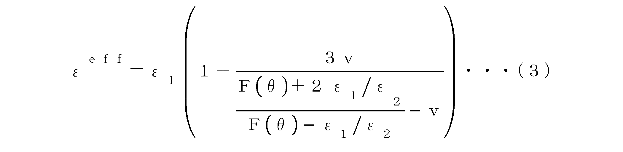

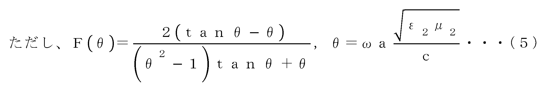

上記(3)~(6)式を用いて、シミュレーションにより磁気損失(QM)を求めたところ、球状粒子及びマトリックスが磁性成分(磁性元素)をもたない場合、即ちμ1=μ2=1の場合であっても、磁気損失(QM)が生じることが分かった。また、この磁気損失(QM)は、球状粒子とマトリックスの誘電率(ε1、ε2)に大きく依存することが分かった。さらに電磁波の周波数(f)が大きくなるにつれ、磁気損失(QM)は急増することが分かった。 When the magnetic loss (Q M ) was calculated by simulation using the above formulas (3) to (6), it was found that magnetic loss (Q M ) occurs even when the spherical particles and matrix do not have a magnetic component (magnetic element), i.e., when μ 1 = μ 2 = 1. It was also found that this magnetic loss (Q M ) is highly dependent on the dielectric constants (ε 1 , ε 2 ) of the spherical particles and matrix. Furthermore, it was found that the magnetic loss (Q M ) increases sharply as the frequency (f) of the electromagnetic wave increases.
このように、誘電率の高い誘電体を用いることで、Mie共鳴に基づく大きな磁気損失が高周波領域で生じることが分かった。またこの磁気損失を電磁波吸収の用途に適用できることが期待された。 In this way, it was found that by using a dielectric with a high dielectric constant, large magnetic loss due to Mie resonance occurs in the high frequency range. It is also expected that this magnetic loss can be applied to electromagnetic wave absorption.
次に本実施形態の誘電体について説明する。誘電体は、高誘電率材料から構成される限り、その材質は限定されない。例えば、チタン酸バリウム(BaTiO3)、チタン酸ストロンチウム(SrTiO3)、チタン酸カルシウム(CaTiO3)、チタン酸ビスマスアルカリ(Bi0.5K0.5TiO3、Bi0.5Na0.5TiO3等)、ニオブ酸アルカリ(NaNbO3、KNbO3等)、鉛系材料(PZT、PMN-PT等)、ビスマス層状化合物(SBT等)などの高誘電率材料を挙げることができる。誘電体は、これらの材料を1種のみ含んでもよく、あるいは複数種の材料を含んでもよい。複数種の材料を含む場合には、混晶の形態で含んでもよく、あるいは固溶体の形態で含んでもよい。誘電体は、チタン酸バリウム(BaTiO3)及びチタン酸ビスマスカリウム(Bi0.5K0.5TiO3)の少なくとも一方を含んでもよい。 Next, the dielectric of this embodiment will be described. The material of the dielectric is not limited as long as it is made of a high dielectric constant material. For example, high dielectric constant materials such as barium titanate (BaTiO 3 ), strontium titanate (SrTiO 3 ), calcium titanate (CaTiO 3 ), bismuth alkali titanate (Bi 0.5 K 0.5 TiO 3 , Bi 0.5 Na 0.5 TiO 3 , etc.), alkali niobate (NaNbO 3 , KNbO 3 , etc.), lead-based materials (PZT, PMN-PT, etc.), and bismuth layered compounds (SBT, etc.) can be mentioned. The dielectric may contain only one of these materials, or may contain multiple types of materials. When multiple types of materials are contained, they may be contained in the form of a mixed crystal or in the form of a solid solution. The dielectric may include at least one of barium titanate (BaTiO 3 ) and bismuth potassium titanate (Bi 0.5 K 0.5 TiO 3 ).
また誘電体は、多結晶でよく、あるいは単結晶であってもよい。さらに誘電体は、誘電材料の乾燥体、成形体又は焼結体であってもよい。ここで乾燥体は、誘電材料を乾燥させて有機溶剤などの液体成分を乾燥させたものであり、また成形体は、誘電材料を成形したものである。さらに焼結体は、成形体を焼結したものである。なお乾燥体において一部の溶剤が残存する懸念がある。したがって、溶剤は残存しにくい沸点の低いものが好ましい。また仮に残存したとしても問題が生じにくい誘電率の高いものが好ましい。ただしペースト中での粉の分散も重要であるため、分散性とのバランスを考えて溶剤を選択すればよい。分散剤についても同様である。 The dielectric may be polycrystalline or single crystalline. The dielectric may be a dried, molded or sintered body of the dielectric material. A dried body is a dielectric material that has been dried to remove liquid components such as organic solvents, and a molded body is a molded dielectric material. A sintered body is a molded body that has been sintered. There is a concern that some of the solvent may remain in the dried body. Therefore, it is preferable for the solvent to have a low boiling point so that it is less likely to remain. It is also preferable for the solvent to have a high dielectric constant so that problems are less likely to occur even if it remains. However, since the dispersion of the powder in the paste is also important, the solvent should be selected while taking into consideration the balance with dispersibility. The same applies to the dispersant.
誘電体は、公知の手法で作製すればよい。例えば、セラミック焼結体である誘電体は、誘電体原料を成形及び焼成して作製すればよい。誘電体原料は、固相反応法、錯体重合法、共沈法、水熱合成法、ゾルゲル法、及び気相法などの公知の手法で合成すればよい。また誘電体原料以外に、成形助剤や焼結助剤などの添加剤を加えてもよい。単結晶である誘電体は、水溶液法、水熱合成法、フラックス法、ベルヌーイ法、チョクラルスキー法、ブリッジマン法、浮遊帯溶融法、スカイメルト法、昇華再結晶法、化学輸送法、及び化学気相成長法などの公知の手法で作製すればよい。 The dielectric may be produced by a known method. For example, a dielectric that is a ceramic sintered body may be produced by molding and firing a dielectric raw material. The dielectric raw material may be synthesized by a known method such as a solid-phase reaction method, a complex polymerization method, a coprecipitation method, a hydrothermal synthesis method, a sol-gel method, or a gas-phase method. In addition to the dielectric raw material, additives such as a molding aid or a sintering aid may be added. A dielectric that is a single crystal may be produced by a known method such as an aqueous solution method, a hydrothermal synthesis method, a flux method, a Bernoulli method, a Czochralski method, a Bridgman method, a floating zone melting method, a skymelt method, a sublimation recrystallization method, a chemical transport method, or a chemical vapor deposition method.
誘電体は、100MHzにおける比誘電率実部εr’が30以上である。高誘電率誘電体を用いることで、この誘電体を備える電磁波吸収体に高い電磁波吸収性能を付与することが可能になる。すなわち、誘電体の誘電率が高いほど、屈折率増大に基づく電磁波の波長短縮効果が大きくなり、より小さい吸収体でMie共鳴が実現する。誘電体の誘電率は高いほど好ましい。εr’は100以上が好ましく、300以上がより好ましい。εr’の上限は特に限定されない、しかしながら、典型的には2000以下、より典型的には1000以下である。なお測定周波数を100MHzに設定した理由は、GHz超の周波数域では測定手法上の問題があり、高誘電率材料の誘電率を精度よく測定することが困難であるからである。 The dielectric has a relative permittivity real part ε r ' at 100 MHz of 30 or more. By using a high permittivity dielectric, it is possible to impart high electromagnetic wave absorption performance to an electromagnetic wave absorber equipped with this dielectric. That is, the higher the permittivity of the dielectric, the greater the wavelength shortening effect of the electromagnetic wave based on the increase in the refractive index, and Mie resonance is realized with a smaller absorber. The higher the permittivity of the dielectric, the more preferable it is. ε r ' is preferably 100 or more, more preferably 300 or more. The upper limit of ε r ' is not particularly limited, but is typically 2000 or less, more typically 1000 or less. The reason for setting the measurement frequency to 100 MHz is that there are problems with the measurement technique in the frequency range above GHz, making it difficult to accurately measure the permittivity of a high permittivity material.
誘電体は、厚さT(単位:μm)に対する直径D(単位:μm)の比(D/T比)が3以上である。本発明者が検討を重ねた結果、扁平形状の誘電体の方が、より薄い吸収体を実現できることが分かった。すなわちD/T比(アスペクト比)を高くすることで、厚みが同じ場合に比べて、より低周波でMie共鳴が生じる。換言するに、Mie共鳴周波数が同じであれば、より薄型の吸収体を実現できる。D/T比は5以上が好ましく、10以上がさらに好ましい。 The ratio (D/T ratio) of the diameter D (unit: μm) to the thickness T (unit: μm) of the dielectric is 3 or more. After extensive research, the inventors found that a flat-shaped dielectric can realize a thinner absorber. In other words, by increasing the D/T ratio (aspect ratio), Mie resonance occurs at a lower frequency compared to the case of the same thickness. In other words, if the Mie resonance frequency is the same, a thinner absorber can be realized. The D/T ratio is preferably 5 or more, and more preferably 10 or more.
本実施形態の電磁波吸収体が備える各誘電体は円板状の形状を有している。すなわち断面が円形である。誘電体の断面は、できるだけ完全な円形に近いほど好ましい。完全な円では径が一定である。しかしながら断面が完全な円形の誘電体は、その製造が困難な場合がある。したがって誘電体は断面が完全な円形であるものに限定されない。各誘電体において、径のバラツキが±10%以下であれば許容される。 Each dielectric in the electromagnetic wave absorber of this embodiment has a disk-like shape. That is, the cross section is circular. It is preferable that the cross section of the dielectric is as close to a perfect circle as possible. A perfect circle has a constant diameter. However, it can be difficult to manufacture a dielectric with a perfectly circular cross section. Therefore, the dielectric is not limited to one with a perfectly circular cross section. For each dielectric, a variation in diameter of ±10% or less is acceptable.
本実施形態のシステムにおいて、電磁波放射源が放射する電磁波の周波数f(単位:Hz)と、円板状誘電体の100MHzにおける比誘電率実部εr’及び厚さT(単位:μm)と、が、下記(1)及び(2)式(ただし、cは光速(3.0×1014μm/秒))を満足する。 In the system of the present embodiment, the frequency f (unit: Hz) of the electromagnetic wave radiated by the electromagnetic wave radiation source, the real part ε r ′ of the relative dielectric constant at 100 MHz and the thickness T (unit: μm) of the disk-shaped dielectric satisfy the following formulas (1) and (2) (where c is the speed of light (3.0× 10 μm/sec)):

![]()
![]()
この点について説明するに、Mie共鳴時の物質はFabry-Perot共振と類似の挙動を示すことが知られている。またFabry-Perot共振において、物質の厚さd’は、共振時の波長λR’及び共振周波数fRと下記(7)式に示す関係を満足することが知られている。なお下記(7)式において、cは光速であり、ε’は物質の比誘電率実部である。 To explain this point, it is known that a material in Mie resonance behaves similarly to a Fabry-Perot resonance. It is also known that in Fabry-Perot resonance, the thickness d' of the material satisfies the relationship shown in the following formula (7) with the wavelength λ R ' and the resonance frequency f R at resonance. In the following formula (7), c is the speed of light, and ε' is the real part of the relative dielectric constant of the material.

Fabry-Perot共振の結果から推論するに、Mie共鳴においても、誘電体の厚さdが上記(7)式の関係を満足する条件、すなわち誘電体の厚さTが共振波長の半波長分(λR’/2)に近い条件で磁気損失が大きくなると期待される。 Inferring from the results of Fabry-Perot resonance, it is expected that magnetic loss will also increase in Mie resonance when the dielectric thickness d satisfies the relationship in equation (7) above, that is, when the dielectric thickness T is close to half the resonant wavelength (λ R '/2).
したがって電磁波吸収体に備えられる誘電体の平均厚さTが上記(2)式を満足する条件で、Mie共鳴に基づく磁気損失が引き起こされ、それにより電磁波が効率的に吸収される。なお上記(2)式において、λ’は誘電体内での電磁波の波長(単位:μm)である。誘電体内での波長は、真空中の電磁波の波長(c/f)に比べて誘電率の平方根に逆比例するように短縮される。また上記(2)式においてTの上限を広くとっているのは、誘電率実部εr’が100MHzで測定した値であるからである。高周波側では誘電率が低下するため、その低下分を見込んでTの上限を幅広くとっている。ただし、温度における吸収周波数の変化を抑える観点では、誘電率の周波数に対する変化は小さいほうが好ましい。つまり上記(7)式に近い関係が保たれていることが好ましい。したがってTは下記(8)式の関係を満足することが好ましく、下記(9)式の関係を満足することがより好ましく、下記(10)式の関係を満足することがさらに好ましい。 Therefore, under the condition that the average thickness T of the dielectric provided in the electromagnetic wave absorber satisfies the above formula (2), magnetic loss based on Mie resonance is induced, and the electromagnetic wave is efficiently absorbed. In the above formula (2), λ' is the wavelength of the electromagnetic wave in the dielectric (unit: μm). The wavelength in the dielectric is shortened in inverse proportion to the square root of the dielectric constant compared to the wavelength (c/f) of the electromagnetic wave in a vacuum. The reason why the upper limit of T is set wide in the above formula (2) is that the real part of the dielectric constant ε r ' is a value measured at 100 MHz. Since the dielectric constant decreases on the high frequency side, the upper limit of T is set wide in anticipation of this decrease. However, from the viewpoint of suppressing the change in the absorption frequency with temperature, it is preferable that the change in the dielectric constant with respect to the frequency is small. In other words, it is preferable that the relationship close to the above formula (7) is maintained. Therefore, it is preferable that T satisfies the relationship of the following formula (8), more preferably the relationship of the following formula (9), and even more preferably the relationship of the following formula (10).
![]()
![]()
![]()
![]()
![]()
![]()
本実施形態の電磁波吸収体は、誘電体メタマテリアルとして働く上記誘電体配置群を備えることで、特定波長の電磁波に対してMie共鳴モードに基づく磁気損失を示す。具体的には、電磁波吸収体は、特定の周波数(fmax;磁気損失最大周波数)で実効的な比透磁率虚部(μ’’ar)及び損失係数(tanδaM)の極大値をもつ。複素比透磁率虚部(μ’’ar)の極大値は0.50以上、1.00以上、または1.50以上であってよい。また損失係数(tanδaM)の極大値は0.50以上、1.00以上、1.50以上、または2.00以上であってよい。 The electromagnetic wave absorber of this embodiment includes the dielectric arrangement group that functions as a dielectric metamaterial, and thus exhibits magnetic loss based on the Mie resonance mode for electromagnetic waves of a specific wavelength. Specifically, the electromagnetic wave absorber has maximum values of the effective imaginary part of relative permeability (μ″ ar ) and loss factor (tan δ aM ) at a specific frequency (f max ; maximum magnetic loss frequency). The maximum value of the imaginary part of complex relative permeability (μ″ ar ) may be 0.50 or more, 1.00 or more, or 1.50 or more. The maximum value of the loss factor (tan δ aM ) may be 0.50 or more, 1.00 or more, 1.50 or more, or 2.00 or more.
電磁波放射源が放射する電磁波の周波数fは、特に限定されない。しかしながら1GHz以上10THz以下が好ましく、3GHz以上5THz以下がより好ましく、10GHz以上1THz以下がさらに好ましく、10GHz以上300GHz以下が特に好ましく、30GHz以上100GHz以下が最も好ましい。周波数fは60GHz以上80GHz以下であってもよい。本実施形態のシステムは、上述した電磁波吸収体を備えることで、GHz帯域における漏洩(不要)電磁波を十分に吸収することができる。具体的には、上記周波数範囲内に電磁波吸収の極大をもたせ、この極大時の反射減衰量の絶対値を10dB以上、15dB以上、または20dB以上にすることができる。 The frequency f of the electromagnetic waves emitted by the electromagnetic wave radiation source is not particularly limited. However, it is preferably 1 GHz to 10 THz, more preferably 3 GHz to 5 THz, even more preferably 10 GHz to 1 THz, particularly preferably 10 GHz to 300 GHz, and most preferably 30 GHz to 100 GHz. The frequency f may be 60 GHz to 80 GHz. The system of this embodiment is equipped with the above-mentioned electromagnetic wave absorber, and can sufficiently absorb leakage (unwanted) electromagnetic waves in the GHz band. Specifically, the electromagnetic wave absorption maximum is set within the above frequency range, and the absolute value of the return loss at this maximum can be 10 dB or more, 15 dB or more, or 20 dB or more.
-第2の態様-
第2の態様における電磁波吸収体は基体と誘電体配置群を備える。この誘電体配置群は複数個の円板状誘電体から構成される。また、この誘電体配置群を構成する各誘電体は、前面及び底面を有し、且つ底面が基体の一表面と対向するように配置される。さらにこの誘電体配置群を構成する誘電体は、100MHzにおける比誘電率実部εr’が30以上、平均直径Dmが100μm以上10000μm以下(0.1mm以上10mm以下)、且つ平均厚さTmが20μm以上300μm以下(0.02mm以上0.3mm以下)である。またこの誘電体は、平均厚さTmに対する平均直径Dmの比(Dm/Tm比)が3以上であり、厚さTの変動係数CVが20%以下である。
-Second aspect-
The electromagnetic wave absorber in the second embodiment includes a base and a dielectric arrangement group. The dielectric arrangement group is composed of a plurality of disk-shaped dielectrics. Each of the dielectrics constituting the dielectric arrangement group has a front surface and a bottom surface, and is arranged so that the bottom surface faces one surface of the base. The dielectrics constituting the dielectric arrangement group have a relative dielectric constant real part εr ' of 30 or more at 100 MHz, an average diameter Dm of 100 μm or more and 10,000 μm or less (0.1 mm or more and 10 mm or less), and an average thickness Tm of 20 μm or more and 300 μm or less (0.02 mm or more and 0.3 mm or less). The ratio of the average diameter Dm to the average thickness Tm ( Dm / Tm ratio) of the dielectric is 3 or more, and the coefficient of variation CV of the thickness T is 20% or less.
第2の態様における電磁波吸収体は、基体を備える。基体は、誘電体を保持する機能を有しており、この機能を有する限り、その材質は限定されない。例えば、樹脂、金属、セラミックスなどが例示される。また、その形状も限定されず、例えば、板、シート、及び箔が例示さる。シート状樹脂基体や箔状金属基体を用いることで、電磁波吸収体に可撓性を付与することが可能になる。また金属基体を用いることで、基体に電磁波反射層としての機能を付与できる。 The electromagnetic wave absorber in the second aspect includes a substrate. The substrate has a function of holding the dielectric, and the material is not limited as long as it has this function. Examples include resin, metal, and ceramics. The shape is also not limited, and examples include a plate, sheet, and foil. By using a sheet-shaped resin substrate or a foil-shaped metal substrate, it is possible to impart flexibility to the electromagnetic wave absorber. Furthermore, by using a metal substrate, the substrate can be given the function of an electromagnetic wave reflecting layer.
第2の態様における電磁波吸収体は、基体の他に、複数個の円板状誘電体から構成される誘電体配置群を備える。この誘電体配置群を構成する各誘電体は、前面及び底面を有し、且つその底面が基体の一表面と対向するように配置されている。すなわち円板状誘電体は、その底面が基体表面に略平行になるように基体上に分散配置されている。円板状誘電体を分散配置させることで、電磁波を効率よく吸収することが可能になる。すなわち、電磁波は、その一部が誘電体の表面で反射される。そのため、入射する電磁波の全てが誘電体中に侵入して減衰する訳ではない。例えば、基体上に誘電体を一様に形成すると、誘電体表面で反射する電磁波の割合が多くなり、吸収特性が低下する恐れがある。これに対して、複数の円板状誘電体を配置すると誘電体間に間隙ができ、この間隙に電磁波が侵入する。間隙に侵入した電磁波が誘電体と共鳴することで吸収が生じる。 The electromagnetic wave absorber in the second aspect includes a base and a dielectric arrangement group consisting of a plurality of disk-shaped dielectrics. Each of the dielectrics constituting the dielectric arrangement group has a front surface and a bottom surface, and is arranged so that its bottom surface faces one surface of the base. That is, the disk-shaped dielectrics are distributed on the base so that their bottom surfaces are approximately parallel to the surface of the base. By distributing the disk-shaped dielectrics, it becomes possible to efficiently absorb electromagnetic waves. That is, a part of the electromagnetic waves is reflected by the surface of the dielectric. Therefore, not all of the incident electromagnetic waves penetrate into the dielectric and are attenuated. For example, if the dielectric is formed uniformly on the base, the proportion of electromagnetic waves reflected by the dielectric surface increases, and there is a risk of the absorption characteristics being reduced. In contrast, when a plurality of disk-shaped dielectrics are arranged, gaps are formed between the dielectrics, and electromagnetic waves penetrate into these gaps. The electromagnetic waves that penetrate into the gaps resonate with the dielectric, causing absorption.
第2の態様において、電磁波吸収体が備える各誘電体は円板状の形状を有している。すなわち断面が円形である。誘電体の断面は、できるだけ完全な円形に近いほど好ましい。完全な円では径が一定である。しかしながら断面が完全な円形の誘電体は、その製造が困難な場合がある。したがって誘電体は断面が完全な円形であるものに限定されない。各誘電体において、径のバラツキが±10%以下であれば許容される。 In the second embodiment, each dielectric in the electromagnetic wave absorber has a disk shape. That is, the cross section is circular. It is preferable that the cross section of the dielectric is as close to a perfect circle as possible. A perfect circle has a constant diameter. However, it may be difficult to manufacture a dielectric with a perfectly circular cross section. Therefore, the dielectric is not limited to a perfectly circular cross section. A variation in diameter of ±10% or less is acceptable for each dielectric.
第2の態様において、誘電体配置群に含まれる誘電体間のサイズ(径)のバラツキが小さいほど好ましい。誘電体サイズ(径)にバラツキが生じると、それぞれの誘電体がもつ共鳴周波数が揃わないため、急峻で深い電磁波吸収特性を得ることが困難になる恐れがある。誘電体の径の大きさのバラツキは±10%以下が好ましい。 In the second aspect, it is preferable that the variation in size (diameter) between the dielectrics included in the dielectric arrangement group is as small as possible. If variation in the dielectric size (diameter) occurs, the resonant frequencies of the respective dielectrics will not be uniform, which may make it difficult to obtain steep and deep electromagnetic wave absorption characteristics. It is preferable that the variation in the diameter of the dielectrics is ±10% or less.
誘電体配置群に含まれる誘電体を規則的に配置してもよく、あるいは不規則に配置してもよい。さらに誘電体の個数も、2個以上であればよい。誘電体の間隙を樹脂などの材料で充填した態様としてもよく、あるいは充填しない態様としてもよい。このように誘電体を配置することで、吸収体表面から入射した電磁波が効率的に誘電体内に侵入し、そこで吸収される。 The dielectrics included in the dielectric arrangement group may be arranged regularly or irregularly. Furthermore, the number of dielectrics may be two or more. The gaps between the dielectrics may be filled with a material such as resin, or may not be filled. By arranging the dielectrics in this way, electromagnetic waves incident on the absorber surface can efficiently penetrate into the dielectrics and be absorbed there.
第2の態様における誘電体の材質や製造方法は、第1の態様における誘電体と同様である。すなわち、誘電体は、高誘電率材料から構成される限り、その材質は限定されない。
また誘電体は、多結晶であってよく、あるいは単結晶であってもよい。誘電体は、誘電材料の乾燥体、成形体又は焼結体であってもよい。さらに誘電体は、公知の手法で作製すればよい。
The material and manufacturing method of the dielectric in the second embodiment are the same as those of the dielectric in the first embodiment. That is, the material of the dielectric is not limited as long as it is made of a high dielectric constant material.
The dielectric may be polycrystalline or single crystalline. The dielectric may be a dried, molded or sintered body of a dielectric material. The dielectric may be produced by a known method.
Fabry-Perot共振の結果から推論するに、第2の態様における誘電体の平均厚さTmを限定することで、例えば30GHz以上1THz以下の周波数域において、Mie共鳴に基づく磁気損失を効果的に利用することができ、その結果、電磁波吸収特性を十分に発揮させることが可能になる。平均厚さTmは30μm以上250μm以下であってよく、50μm以上200μm以下であってよく、70μm以上150μm以下であってもよい。 Inferred from the results of Fabry-Perot resonance, by limiting the average thickness Tm of the dielectric material in the second embodiment, it is possible to effectively utilize the magnetic loss based on Mie resonance in the frequency range of, for example, 30 GHz to 1 THz, and as a result, it is possible to fully exhibit the electromagnetic wave absorption characteristics. The average thickness Tm may be 30 μm to 250 μm, 50 μm to 200 μm, or 70 μm to 150 μm.
第2の態様において、誘電体配置群を構成する誘電体は、平均直径Dmが100μm以上10000μm以下(0.1mm以上10mm以下)である。本発明者が調べたところ、第2の態様における円板状誘電体の径を入射電磁波の波長より小さくすることで、電磁波の吸収効率を最大にできることが分かった。すなわち先述したように、複数の円板状誘電体を配置することで、誘電体間に間隙ができる。この間隙に電磁波が侵入することで電磁波吸収が効率的に行われる。入射する電磁波の波長より誘電体の径を小さくすることで、誘電体間の間隙への電磁波の侵入が促進され、その結果、誘電体の共鳴現象がより顕著に起こる。平均直径Dmは200μm以上5000μm以下であってよく、300μm以上3000μm以下であってよく、500μm以上2000μm以下であってもよい。 In the second embodiment, the dielectrics constituting the dielectric arrangement group have an average diameter Dm of 100 μm or more and 10,000 μm or less (0.1 mm or more and 10 mm or less). The inventors have investigated and found that the efficiency of absorbing electromagnetic waves can be maximized by making the diameter of the disk-shaped dielectrics in the second embodiment smaller than the wavelength of the incident electromagnetic waves. That is, as described above, by arranging a plurality of disk-shaped dielectrics, gaps are formed between the dielectrics. The electromagnetic waves penetrate into these gaps, and thus electromagnetic wave absorption is efficiently performed. By making the diameter of the dielectrics smaller than the wavelength of the incident electromagnetic waves, the penetration of the electromagnetic waves into the gaps between the dielectrics is promoted, and as a result, the resonance phenomenon of the dielectrics occurs more significantly. The average diameter Dm may be 200 μm or more and 5,000 μm or less, 300 μm or more and 3,000 μm or less, or 500 μm or more and 2,000 μm or less.
第2の態様において、誘電体配置群を構成する誘電体は、平均厚さTmに対する平均直径Dmの比(Dm/Tm比)が3以上である。Dm/Tm比(アスペクト比)を高くすることで、厚みが同じ場合に比べて、より低周波でMie共鳴が生じる。つまり、より薄型の吸収体が実現される。Dm/Tm比は5以上が好ましく、10以上がさらに好ましい。 In the second aspect, the dielectrics constituting the dielectric arrangement group have a ratio of average diameter Dm to average thickness Tm ( Dm / Tm ratio) of 3 or more. By increasing the Dm / Tm ratio (aspect ratio), Mie resonance occurs at a lower frequency compared to the case where the thickness is the same. In other words, a thinner absorber is realized. The Dm / Tm ratio is preferably 5 or more, and more preferably 10 or more.
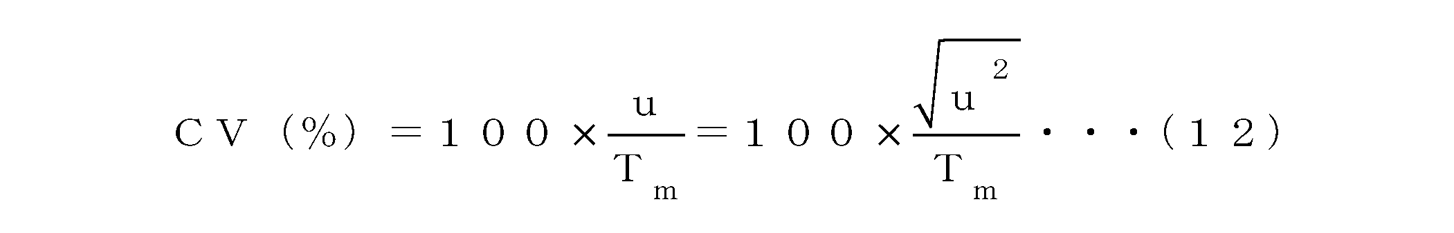
第2の態様において、誘電体配置群は、これを構成する誘電体の厚さTの変動係数CVが20%以下である。ここで変動係数CVはバラツキの指標となるものである。すなわち誘電体配置群を構成する誘電体間での厚さのバラツキを小さくすることで、それぞれの誘電体がもつ共鳴周波数が揃う。そのため、より急峻で深い電磁波吸収特性を得ることができる。変動係数は15%以下が好ましく、10%以下がさらに好ましい。なお変動係数CVは、誘電体配置群を構成する個々の誘電体の厚さTiと平均厚さTmとを用いて、下記(11)式及び(12)式にしたがって求められる。なお下記(11)式及び(12)式において、nは誘電体配置群を構成する誘電体の個数、u2は厚さの不偏分散(標本分散)、uは厚さの標本標準偏差である。 In the second embodiment, the dielectric arrangement group has a coefficient of variation CV of thickness T of the dielectrics constituting the dielectric arrangement group of 20% or less. Here, the coefficient of variation CV is an index of variation. That is, by reducing the variation in thickness between the dielectrics constituting the dielectric arrangement group, the resonance frequencies of the respective dielectrics are uniform. Therefore, it is possible to obtain a steeper and deeper electromagnetic wave absorption characteristic. The coefficient of variation is preferably 15% or less, and more preferably 10% or less. The coefficient of variation CV is calculated according to the following formulas (11) and (12) using the thickness T i and the average thickness T m of each dielectric constituting the dielectric arrangement group. In the following formulas (11) and (12), n is the number of dielectrics constituting the dielectric arrangement group, u 2 is the unbiased variance (sample variance) of the thickness, and u is the sample standard deviation of the thickness.

第2の態様において、好ましくは、誘電体配置群を構成する誘電体の面積割合は10%以上90%以下である。ここで誘電体の面積割合とは、基体表面のうち誘電体が分散配置されている領域の総面積に対する、誘電体前面(または底面)の合計面積の割合のことである。すなわち電磁波吸収体を上方から見たときに誘電体が占める面積の割合のことである。面積割合を10%以上にすると、磁気共鳴(Mie共鳴)を起す誘電体の割合が大きくなる結果、電磁波吸収特性がより優れたものになる。また面積割合を90%以下にすることで、誘電体間に十分な間隙を設けることができるため、この間隙に侵入した電磁波が引き起こす磁気共鳴現象を十分に利用することができる。そのため電磁波吸収特性が優れたものになる。面積割合は10%以上75%以下であってよく、10%以上50%以下であってもよい。 In the second embodiment, the area ratio of the dielectrics constituting the dielectric arrangement group is preferably 10% or more and 90% or less. Here, the area ratio of the dielectrics refers to the ratio of the total area of the front surface (or bottom surface) of the dielectrics to the total area of the region on the substrate surface where the dielectrics are distributed. In other words, it refers to the ratio of the area occupied by the dielectrics when the electromagnetic wave absorber is viewed from above. If the area ratio is 10% or more, the ratio of the dielectrics that cause magnetic resonance (Mie resonance) increases, resulting in better electromagnetic wave absorption characteristics. Furthermore, by setting the area ratio to 90% or less, sufficient gaps can be provided between the dielectrics, so that the magnetic resonance phenomenon caused by the electromagnetic waves that penetrate into these gaps can be fully utilized. Therefore, the electromagnetic wave absorption characteristics are excellent. The area ratio may be 10% or more and 75% or less, or may be 10% or more and 50% or less.
第2の態様において、好ましくは、誘電体配置群を構成する誘電体の個数面密度は3個/cm2以上である。ここで個数密度とは、基体表面のうち誘電体が分散配置されている領域の総面積に対する、誘電体の総個数の比である。すなわち電磁波吸収体を上方から見たときに単位面積当たりの誘電体の個数のことである。個数面密度を高めることで、磁気共鳴(Mie共鳴)を起す誘電体の割合が高くなり、その結果、電磁波吸収特性がより優れたものになる。個数面密度は15個/cm2以上が好ましく、30個/cm2以上がより好ましい。 In the second embodiment, the number surface density of the dielectrics constituting the dielectric arrangement group is preferably 3 pieces/ cm2 or more. Here, the number density is the ratio of the total number of dielectrics to the total area of the region in which the dielectrics are dispersed on the surface of the substrate. That is, it is the number of dielectrics per unit area when the electromagnetic wave absorber is viewed from above. By increasing the number surface density, the proportion of dielectrics that cause magnetic resonance (Mie resonance) increases, resulting in better electromagnetic wave absorption characteristics. The number surface density is preferably 15 pieces/cm2 or more , more preferably 30 pieces/cm2 or more .
第2の態様において、好ましくは、誘電体配置群を構成する誘電体の誘電正接(tanδ)は0.03以上である。誘電正接の高い誘電体を用いることで、Mie共鳴時の磁気損失が大きくなるとともに誘電損失も電磁波吸収に利用することができる。そのため、電磁波吸収特性がより一層優れたものになると期待される。誘電正接は0.06以上、0.09以上、または0.12以上であってもよい。 In the second embodiment, the dielectric loss tangent (tan δ) of the dielectrics constituting the dielectric arrangement group is preferably 0.03 or more. By using a dielectric with a high dielectric loss tangent, the magnetic loss during Mie resonance increases and the dielectric loss can also be utilized for electromagnetic wave absorption. Therefore, it is expected that the electromagnetic wave absorption characteristics will be even better. The dielectric loss tangent may be 0.06 or more, 0.09 or more, or 0.12 or more.
第2の態様において、電磁波放射源が放射する電磁波の周波数f(単位:Hz)と、電磁波吸収体が備える誘電体の比誘電率実部εr’、平均直径Dm(単位:μm)及び厚さTm(単位:μm)と、は、下記(13)~(16)式を満足する。なお下記(13)及び(14)式において、cは光速(3.0×1014μm/秒=3.0×108m/秒)である。 In a second aspect, the frequency f (unit: Hz) of the electromagnetic wave radiated by the electromagnetic wave radiation source, and the real part ε r ' of the relative dielectric constant, average diameter D m (unit: μm) and thickness T m (unit: μm) of the dielectric of the electromagnetic wave absorber satisfy the following formulas (13) to (16). Note that in the following formulas (13) and (14), c is the speed of light (3.0×10 14 μm/sec=3.0×10 8 m/sec).


![]()
![]()
![]()
![]()
この点について説明するに、第2の態様において、第1の態様の場合と同様に誘電体の厚さ(T)が共振波長の半波長(λR’/2)に近似しているときに磁気損失が生じる。したがって電磁波吸収体に備えられる複数の誘電体の平均厚さTmが上記(16)式を満足する条件で、Mie共鳴に基づく磁気損失が引き起こされ、それにより電磁波が効率的に吸収される。なお上記(16)式において、λ’は誘電体内での電磁波の波長(単位:μm)である。誘電体内での波長は、真空中の電磁波の波長(c/f)に比べて誘電率の平方根に逆比例するように短縮される。また上記(16)式においてTmの上限を広くとっているのは、誘電率実部εr’が100MHzで測定した値であるからである。高周波側では誘電率が低下するため、その低下分を見込んでTmの上限を幅広くとっている。ただし、温度における吸収周波数の変化を抑える観点では、誘電率の周波数に対する変化は小さいほうが好ましい。つまり上記(7)式に近い関係が保たれていることが好ましい。したがってTmは下記(17)式の関係を満足することが好ましく、下記(18)式の関係を満足することがより好ましく、下記(19)式の関係を満足することがさらに好ましい。 To explain this point, in the second embodiment, magnetic loss occurs when the thickness (T) of the dielectric is close to half the wavelength (λ R '/2) of the resonance wavelength, as in the first embodiment. Therefore, under the condition that the average thickness T m of the plurality of dielectrics provided in the electromagnetic wave absorber satisfies the above formula (16), magnetic loss based on Mie resonance is induced, and the electromagnetic wave is efficiently absorbed. In the above formula (16), λ ' is the wavelength (unit: μm) of the electromagnetic wave in the dielectric. The wavelength in the dielectric is shortened so as to be inversely proportional to the square root of the dielectric constant compared to the wavelength (c/f) of the electromagnetic wave in a vacuum. In addition, the upper limit of T m is set wide in the above formula (16) because the real part of the dielectric constant ε r ' is a value measured at 100 MHz. Since the dielectric constant decreases on the high frequency side, the upper limit of T m is set wide in anticipation of this decrease. However, from the viewpoint of suppressing the change in the absorption frequency with temperature, it is preferable that the change in the dielectric constant with respect to the frequency is small. That is, it is preferable that a relationship close to the above formula (7) is maintained. Therefore, Tm preferably satisfies the relationship of the following formula (17), more preferably satisfies the relationship of the following formula (18), and further preferably satisfies the relationship of the following formula (19).
![]()
![]()
![]()
![]()
![]()
![]()
第2の態様において、上述したように、入射する電磁波の波長より誘電体の径を小さくすることで、電磁波吸収を効率的に行える。したがって電磁波吸収体に備えられる複数の誘電体の平均直径Dmが上記(15)式を満足する条件で電磁波の吸収効率が改善される。なお上記(15)式において、λは真空下での電磁波の波長(単位:μm)であり、これは大気下での波長と殆ど同じである。Dmは下記(20)式の関係を満足することが好ましく、下記(21)式の関係を満足することがより好ましく、下記(22)式の関係を満足することがさらに好ましい。 In the second aspect, as described above, the diameter of the dielectric is made smaller than the wavelength of the incident electromagnetic wave, so that electromagnetic wave absorption can be performed efficiently. Therefore, the electromagnetic wave absorption efficiency is improved under the condition that the average diameter Dm of the plurality of dielectrics provided in the electromagnetic wave absorber satisfies the above formula (15). In the above formula (15), λ is the wavelength (unit: μm) of the electromagnetic wave in a vacuum, which is almost the same as the wavelength in the atmosphere. Dm preferably satisfies the relationship of the following formula (20), more preferably satisfies the relationship of the following formula (21), and even more preferably satisfies the relationship of the following formula (22).
![]()
![]()
![]()
![]()
![]()
![]()
第2の態様において、電磁波放射源が放射する電磁波の周波数fは、特に限定されない。しかしながら1GHz以上10THz以下が好ましく、3GHz以上5THz以下がより好ましく、10GHz以上1THz以下がさらに好ましく、10GHz以上300GHz以下が特に好ましく、30GHz以上100GHz以下が最も好ましい。周波数fは60GHz以上80GHz以下であってもよい。本実施形態のシステムは、上述した電磁波吸収体を備えることで、GHz帯域における漏洩(不要)電磁波を十分に吸収することができる。具体的には、上記周波数範囲内に電磁波吸収の極大をもたせ、この極大時の反射減衰量の絶対値を10dB以上、15dB以上、または20dB以上にすることができる。 In the second aspect, the frequency f of the electromagnetic waves emitted by the electromagnetic wave radiation source is not particularly limited. However, it is preferably 1 GHz to 10 THz, more preferably 3 GHz to 5 THz, even more preferably 10 GHz to 1 THz, particularly preferably 10 GHz to 300 GHz, and most preferably 30 GHz to 100 GHz. The frequency f may be 60 GHz to 80 GHz. The system of this embodiment is provided with the above-mentioned electromagnetic wave absorber, and can sufficiently absorb leakage (unwanted) electromagnetic waves in the GHz band. Specifically, the electromagnetic wave absorption maximum is set within the above frequency range, and the absolute value of the return loss at this maximum can be 10 dB or more, 15 dB or more, or 20 dB or more.
第1の態様及び第2の態様のいずれであっても、電磁波吸収体は基体と誘電体配置群以外の他の部材を含んでもよい。例えば表面にインピーダンス整合層や表面保護層を設けてもよい。また裏面に反射部材を設けてもよい。インピーダンス整合層として、磁性粉や誘電体粉末を樹脂中に分散させた層が例示される。表面保護層として、樹脂やガラスからなる層が例示される。反射部材として、膜状、箔状、板状、または網状の金属部材が挙げられる。 In either the first or second embodiment, the electromagnetic wave absorber may include other members in addition to the substrate and the dielectric arrangement group. For example, an impedance matching layer or a surface protection layer may be provided on the surface. A reflective member may also be provided on the back surface. An example of the impedance matching layer is a layer in which magnetic powder or dielectric powder is dispersed in a resin. An example of the surface protection layer is a layer made of resin or glass. An example of the reflective member is a film-like, foil-like, plate-like, or mesh-like metal member.
2.電磁波吸収方法
本実施形態の電磁波の吸収方法は、電磁波吸収体を用いる。また、この電磁波吸収体は円板状誘電体を備える。この円板状誘電体は、100MHzにおける比誘電率実部εr’が30以上、且つ厚さT(単位:μm)に対する直径D(単位:μm)の比(D/T比)が3以上である。さらに電磁波の周波数f(単位:Hz)と、円板状誘電体の100MHzにおける比誘電率実部εr’及び厚さT(単位:μm)と、が、下記(1)及び(2)式(ただし、cは光速(3.0×1014μm/秒))を満足する。
2. Electromagnetic Wave Absorption Method The electromagnetic wave absorption method of this embodiment uses an electromagnetic wave absorber. The electromagnetic wave absorber includes a disk-shaped dielectric. The disk-shaped dielectric has a relative dielectric constant real part ε r ' at 100 MHz of 30 or more, and a ratio (D/T ratio) of diameter D (unit: μm) to thickness T (unit: μm) of 3 or more. Furthermore, the frequency f (unit: Hz) of the electromagnetic wave, the relative dielectric constant real part ε r ' at 100 MHz and thickness T (unit: μm) of the disk-shaped dielectric satisfy the following formulas (1) and (2) (where c is the speed of light (3.0×10 14 μm/sec)).

![]()
![]()
本実施形態の電磁波の吸収方法の詳細は、本実施形態のシステムについて説明したとおりである。すなわち電磁波は、伝送線路、高周波回路、電子素子、電子部品、電子機器、レーダー、及び/又はケーブルなどの電磁波放射源が放射する漏洩電磁波である。また電磁波吸収体の詳細は、上述した第1及び第2態様のいずれかにおける電磁波吸収体と同様である。 Details of the electromagnetic wave absorption method of this embodiment are as described for the system of this embodiment. That is, the electromagnetic waves are leakage electromagnetic waves emitted from electromagnetic wave radiation sources such as transmission lines, high-frequency circuits, electronic elements, electronic components, electronic devices, radar, and/or cables. Details of the electromagnetic wave absorber are the same as those of the electromagnetic wave absorber in either the first or second aspect described above.
電磁波の周波数fは、特に限定されない。しかしながら1GHz以上10THz以下が好ましく、3GHz以上5THz以下がより好ましく、10GHz以上1THz以下がさらに好ましく、10GHz以上300GHz以下が特に好ましく、30GHz以上100GHz以下が最も好ましい。周波数fは60GHz以上80GHz以下であってもよい。本実施形態の方法は、上述した電磁波吸収体を用いることで、GHz帯域における不要電磁波を十分に吸収することができる。具体的には、上記周波数範囲内に電磁波吸収の極大をもたせ、この極大時の反射減衰量の絶対値を10dB以上、15dB以上、または20dB以上にすることができる。 The frequency f of the electromagnetic wave is not particularly limited. However, it is preferably 1 GHz or more and 10 THz or less, more preferably 3 GHz or more and 5 THz or less, even more preferably 10 GHz or more and 1 THz or less, particularly preferably 10 GHz or more and 300 GHz or less, and most preferably 30 GHz or more and 100 GHz or less. The frequency f may be 60 GHz or more and 80 GHz or less. The method of this embodiment can sufficiently absorb unnecessary electromagnetic waves in the GHz band by using the above-mentioned electromagnetic wave absorber. Specifically, it is possible to provide a maximum of electromagnetic wave absorption within the above frequency range, and to set the absolute value of the return loss at this maximum to 10 dB or more, 15 dB or more, or 20 dB or more.
このような本実施形態によれば、誘電体のMie共鳴に基づく磁気損失を利用した電磁波吸収体を備えたシステム、及びこの電磁波吸収体を用いた電磁波吸収方法が実現される。このシステム及び吸収方法には様々な利点がある。 According to this embodiment, a system is realized that includes an electromagnetic wave absorber that utilizes magnetic loss based on the Mie resonance of a dielectric, and an electromagnetic wave absorption method that uses this electromagnetic wave absorber. This system and absorption method have various advantages.
従来の電磁波吸収体では、誘電材料の誘電特性、及び/又は磁性材料の磁気特性を利用して電磁波吸収を図っている。具体的には、誘電材料の誘電損失や磁性材料の磁気損失を利用して電磁波エネルギーを熱エネルギーに変換している。また誘電材料の誘電率と磁性材料の透磁率を個別に制御することで、材料の特性インピーダンスを外部環境の特性インピーダンスと整合させ、それにより吸収体表面での電磁波反射を防いでいる。 Conventional electromagnetic wave absorbers attempt to absorb electromagnetic waves by utilizing the dielectric properties of dielectric materials and/or the magnetic properties of magnetic materials. Specifically, they convert electromagnetic wave energy into thermal energy by utilizing the dielectric loss of the dielectric material and the magnetic loss of the magnetic material. In addition, by individually controlling the dielectric constant of the dielectric material and the magnetic permeability of the magnetic material, the characteristic impedance of the material is matched to the characteristic impedance of the external environment, thereby preventing electromagnetic wave reflection on the absorber surface.
しかしながら、スネーク(Snoek)の限界によれば、磁性材料の高い磁気特性を高周波まで維持することは困難である。そのため従来の材料では、特にGHz以上の高周波域で高い吸収特性を得る上で限界があった。また電磁波吸収体の背面に金属板を設置して、吸収体表面での反射波と吸収体表面での反射波を干渉させることで電磁波を減衰させる手法も知られているが、この手法では、吸収周波数が電磁波の入射角に強く依存するという問題があった。 However, according to Snoek's limit, it is difficult to maintain the high magnetic properties of magnetic materials up to high frequencies. Therefore, conventional materials have limitations in obtaining high absorption properties, especially in the high frequency range of GHz and above. There is also a known method of attenuating electromagnetic waves by placing a metal plate on the back of the electromagnetic wave absorber and causing interference between the waves reflected on the absorber surface, but this method has the problem that the absorption frequency is strongly dependent on the angle of incidence of the electromagnetic waves.
これに対して、本実施形態のシステムや吸収方法は、誘電体のMie共鳴に基づく磁気損失を利用している、強磁性体を用いていないためスネークの限界の縛りを受けず、高周波域まで高い吸収性能を維持することが可能である。また共振周波数の電磁波入射角依存性が小さいため、様々な方向から入射する電磁波に対処できるという利点がある。 In contrast, the system and absorption method of this embodiment utilizes magnetic loss based on the Mie resonance of the dielectric, and since it does not use a ferromagnetic material, it is not bound by the snake's limit and can maintain high absorption performance up to the high frequency range. In addition, since the resonant frequency has little dependence on the electromagnetic wave incident angle, it has the advantage of being able to handle electromagnetic waves incident from various directions.
その上、本実施形態のシステムや吸収方法で用いられる電磁波吸収体は、複数個の円板状誘電体を備えている。また限定されるものではないが、入射する電磁波の波長より誘電体の直径を小さくするとともに、誘電体の面積割合を90%以下に限定している。そして、これらにより電磁波吸収特性がより一層優れたものになる。すなわち複数個の誘電体を設けることで誘電体間に間隙ができる。そして誘電体の直径を小さくするとともに、適度に疎となるように誘電体を配置することで、電磁波がこの間隙に侵入して、誘電体のMie共鳴が効果的に発現されるようになる。これに対して、従来の電磁波吸収体は、Mie共鳴を利用していない。そのため、通常は占有率を上げるため吸収物質を一面に配置する。つまり本実施形態とは異なり、吸収物質は適度に疎になるように配置されていない。 Furthermore, the electromagnetic wave absorber used in the system and absorption method of this embodiment has multiple disk-shaped dielectrics. Although not limited to this, the diameter of the dielectric is smaller than the wavelength of the incident electromagnetic wave, and the area ratio of the dielectric is limited to 90% or less. This makes the electromagnetic wave absorption characteristics even better. In other words, by providing multiple dielectrics, gaps are created between the dielectrics. By reducing the diameter of the dielectrics and arranging the dielectrics so that they are moderately sparse, the electromagnetic waves penetrate into these gaps, and the Mie resonance of the dielectrics is effectively expressed. In contrast, conventional electromagnetic wave absorbers do not use Mie resonance. Therefore, the absorbing material is usually arranged on one surface to increase the occupancy rate. In other words, unlike this embodiment, the absorbing material is not arranged so that it is moderately sparse.
Mie共鳴に基づく磁気損失を利用する本実施形態のシステム、及び電磁波吸収方法は、従来は全くなかったコンセプトに基づくものであり、学術的にも産業的にも画期的なものである。 The system and electromagnetic wave absorption method of this embodiment, which utilizes magnetic loss due to Mie resonance, is based on a completely unprecedented concept and is groundbreaking both academically and industrially.
(1)電磁波吸収体の作製
[例1]
例1では、チタン酸バリウム(BTO;BaTiO3)焼結体を誘電体として用いて電磁波吸収体を作製した。
(1) Preparation of electromagnetic wave absorber [Example 1]
In Example 1, an electromagnetic wave absorber was produced using a barium titanate (BTO; BaTiO 3 ) sintered body as a dielectric.
誘電体原料としてD50が60nmのチタン酸バリウム粉末、溶剤としてネオペンチルグルコールジオレート(日油株式会社、ユニスターHP281R)、及び分散剤(Lubrizol社、HPA-N107)を下記表1に示す配合組成が得られるように秤量し、自公転ミキサーを用いて混錬した。これによりペーストを作製した。 Barium titanate powder with a D50 of 60 nm was used as the dielectric raw material, neopentyl glycol diolate (NOF Corporation, Unistar HP281R) was used as the solvent, and a dispersant (Lubrizol, HPA-N107) was weighed out to obtain the composition shown in Table 1 below, and kneaded using a planetary mixer. This produced a paste.
次いで、複数個の円形の穴(φ1.2mm)を設けたメタルマスク(厚み150μm)をアルミナ板上に置き、作製したペーストをメタルマスク上に塗布した。その後、メタルマスクを外して、アルミナ上に厚さ150μmのペーストパターンを形成した。そして、作製したペーストパターンを1025℃×3時間の条件で焼成して、複数個のチタン酸バリウム焼結体を誘電体として得た。 Next, a metal mask (thickness 150 μm) with multiple circular holes (φ1.2 mm) was placed on the alumina plate, and the prepared paste was applied onto the metal mask. The metal mask was then removed, and a paste pattern with a thickness of 150 μm was formed on the alumina. The prepared paste pattern was then fired under conditions of 1025°C x 3 hours, to obtain multiple barium titanate sintered bodies as dielectrics.
得られたチタン酸バリウム焼結体5200個をポリエチレンテレフタレート(PET)フィルム(12cm×12cm×0.05mm)上にランダムに配置し、その間隙にエポキシ樹脂を注入及び硬化させて、電磁波吸収体を作製した。得られた電磁波吸収体の特性を下記表3に示す。 5,200 pieces of the obtained barium titanate sintered bodies were randomly arranged on a polyethylene terephthalate (PET) film (12 cm x 12 cm x 0.05 mm), and epoxy resin was injected into the gaps and cured to produce an electromagnetic wave absorber. The properties of the obtained electromagnetic wave absorber are shown in Table 3 below.
[例2]
例2では、チタン酸バリウム(BTO;BaTiO3)焼結体を誘電体として用いて電磁波吸収体を作製した。
[Example 2]
In Example 2, an electromagnetic wave absorber was produced using a barium titanate (BTO; BaTiO 3 ) sintered body as a dielectric.
誘電体原料として、粒径(D50)の異なる3種類のチタン酸バリウム粉末を用いた。また誘電体原料、溶剤及び分散剤の秤量を、下記表1に示す配合組成が得られるように行った。さらにメタルマスクの厚みを125μmに変えて、厚さ125μmのペーストパターンを形成した。それ以外は例1と同様にして電磁波吸収体を作製した。 Three types of barium titanate powder with different particle sizes (D50) were used as the dielectric raw material. The dielectric raw material, solvent, and dispersant were weighed out so as to obtain the composition shown in Table 1 below. Furthermore, the thickness of the metal mask was changed to 125 μm, and a paste pattern with a thickness of 125 μm was formed. Otherwise, the electromagnetic wave absorber was produced in the same manner as in Example 1.
[例3]
例3では、チタン酸バリウム(BTO;BaTiO3)成形体を誘電体として用いて電磁波吸収体を作製した。
[Example 3]
In Example 3, an electromagnetic wave absorber was produced using a barium titanate (BTO; BaTiO 3 ) compact as a dielectric.
複数個の円形の穴(φ1.2mm)を設けたメタルマスク(厚み125μm)をPETフィルム(12cm×12cm×0.05mm)上に置き、例2で得られたペーストをメタルマス上に塗布した。その後、メタルマスクを外して、PETフィルム上に厚さ125μmのペーストパターンを形成した。得られたペーストパターンを200℃で減圧乾燥して溶剤の一部を揮発除去させた。このようにしてPET上にチタン酸バリウム成形体2500個を誘電体として作製した。その後、成形体の間隙にエポキシ樹脂を注入及び硬化させて電磁波吸収体を作製した。例3では、例1と異なり、誘電体の配置はメタルマスクの規則的なペーストパターンを維持しており、ランダム配置にはなっていない。 A metal mask (thickness 125 μm) with multiple circular holes (φ1.2 mm) was placed on a PET film (12 cm × 12 cm × 0.05 mm), and the paste obtained in Example 2 was applied onto the metal mask. The metal mask was then removed, and a paste pattern with a thickness of 125 μm was formed on the PET film. The resulting paste pattern was dried under reduced pressure at 200°C to volatilize and remove part of the solvent. In this way, 2,500 barium titanate molded bodies were produced as dielectrics on the PET. Then, epoxy resin was injected into the gaps between the molded bodies and cured to produce an electromagnetic wave absorber. In Example 3, unlike Example 1, the arrangement of the dielectrics maintains the regular paste pattern of the metal mask and is not randomly arranged.
[例4]
例4では、チタン酸バリウムストロンチウム(BSTO;Ba0.8Sr0.2TiO3)焼結体を誘電体として用いて電磁波吸収体を作製した。
[Example 4]
In Example 4, an electromagnetic wave absorber was produced using a barium strontium titanate (BSTO; Ba 0.8 Sr 0.2 TiO 3 ) sintered body as a dielectric.
誘電体原料としてチタン酸バリウムストロンチウム(Ba0.8Sr0.2TiO3)粉末を用いた。まず炭酸バリウム(BaTiO3)、炭酸ストロンチウム(SrCO3)及び酸化チタン(TiO2)を用いて固相反応法でチタン酸バリウムストロンチウム粉末を合成した。次いで、誘電体原料、溶剤及び分散剤を下記表1に示す配合組成が得られるように秤量し、自公転ミキサーを用いて混錬した。これによりペーストを作製した。 Barium strontium titanate ( Ba0.8Sr0.2TiO3 ) powder was used as the dielectric raw material. First , barium strontium titanate powder was synthesized by a solid-state reaction method using barium carbonate ( BaTiO3 ), strontium carbonate ( SrCO3 ) and titanium oxide ( TiO2 ). Next, the dielectric raw material, solvent and dispersant were weighed so as to obtain the composition shown in Table 1 below, and kneaded using a planetary mixer. This produced a paste.
次いで、複数個の円形の穴(φ1.2mm)を設けたメタルマスク(厚み100μm)をアルミナ板上に置き、作製したペーストをメタルマスク上に塗布した。その後、メタルマスクを外して、アルミナ上に厚さ100μmのペーストパターンを形成した。そして、作製したペーストパターンを1200℃×3時間の条件で焼成して、複数個のチタン酸バリウムストロンチウム焼結体を誘電体として得た。 Next, a metal mask (thickness 100 μm) with multiple circular holes (φ1.2 mm) was placed on the alumina plate, and the prepared paste was applied onto the metal mask. After that, the metal mask was removed, and a paste pattern with a thickness of 100 μm was formed on the alumina. The prepared paste pattern was then fired under conditions of 1200°C x 3 hours, to obtain multiple barium strontium titanate sintered bodies as dielectrics.
得られたチタン酸バリウムストロンチウム焼結体をポリエチレンテレフタレート(PET)フィルム上にランダムに配置し、その間隙にエポキシ樹脂を注入及び硬化させて、電磁波吸収体を作製した。 The obtained barium strontium titanate sintered bodies were randomly arranged on a polyethylene terephthalate (PET) film, and epoxy resin was injected into the gaps and cured to produce an electromagnetic wave absorber.

(2)評価
例1~例4について、各種特性の評価を以下のとおり行った。
(2) Evaluation Regarding Examples 1 to 4, various characteristics were evaluated as follows.
<誘電体の寸法>
例1~例4のそれぞれについて、ペーストパターンの直径を誘電体の平均直径Dmと見なした。焼成後の直径方向の収縮は小さいため、ペーストパターンの直径と焼結体の直径を同一視できるからである。厚みについては、得られた複数個の誘電体(焼結体、成形体)から無作為に20個の誘電体を選び、各誘電体の中心部における厚みTi(i=1,2・・・20)をレーザー顕微鏡で測定し、その平均値Tmを求めた。そして、上記(11)式及び(12)に従って、厚さの変動係数CVを求めた。
<Dimensions of dielectric>
For each of Examples 1 to 4, the diameter of the paste pattern was regarded as the average diameter Dm of the dielectric. This is because the shrinkage in the diameter direction after firing is small, and the diameter of the paste pattern can be regarded as the same as the diameter of the sintered body. Regarding the thickness, 20 dielectrics were randomly selected from the obtained multiple dielectrics (sintered bodies, compacts), and the thickness T i (i=1, 2...20) at the center of each dielectric was measured with a laser microscope, and the average value T m was obtained. Then, the coefficient of variation CV of the thickness was obtained according to the above formulas (11) and (12).
<誘電体の誘電特性>
例1~例4で得られた誘電体について、100MHzにおける誘電特性を測定した。具体的には以下の手順で測定を行った。まず誘電体の両面に銀ペーストを塗布して電極を形成してサンプルを作製した。次いで、電圧電流法でサンプルのインピーダンスを求め、得られたインピーダンスを解析してキャパシタ成分及び抵抗成分を求めた。そしてサンプル厚み及び電極面積を用いて、キャパシタ成分及び抵抗成分から複素比誘電率(εr=εr’-jεr’’)を算出した。ここで、εr’とεr’’は、それぞれ複素比誘電率の実部と虚部である。また複素比誘電率の実部εr’と虚部εr’’を用いて、誘電正接(tanδ)下記(23)式にしたがって求めた。
<Dielectric properties of dielectric materials>
The dielectric properties at 100 MHz were measured for the dielectrics obtained in Examples 1 to 4. Specifically, the measurements were performed in the following procedure. First, a sample was prepared by applying silver paste to both sides of the dielectric to form electrodes. Next, the impedance of the sample was obtained by a voltage-current method, and the obtained impedance was analyzed to obtain the capacitor component and the resistor component. Then, the complex dielectric constant (ε r = ε r '-jε r '') was calculated from the capacitor component and the resistor component using the sample thickness and the electrode area. Here, ε r ' and ε r '' are the real part and the imaginary part of the complex dielectric constant, respectively. In addition, the dielectric loss tangent (tan δ) was calculated according to the following formula (23) using the real part ε r ' and the imaginary part ε r '' of the complex dielectric constant.

<電磁波吸収体の特性>
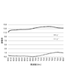
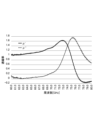
例1~例4で得られた電磁波吸収体について、60~80GHzにおける複素比誘電率、複素比透磁率、及び電磁波吸収特性の測定を、以下の手順で行った。すなわち、自由空間法により、ベクトルネットワークアナライザ(アンリツ株式会社、ME7838A)を用いてサンプルの反射特性及び透過特性を測定し、得られた反射特性と透過特性から複素比誘電率(εar=εar’-jεar’’)と複素比透磁率(μar=μar’-jμar’’)を算出した。ここでεarとμarのそれぞれは電磁波吸収体全体の実効複素比誘電率と実効比透磁率であり、誘電体の複素誘電率εr及び複素比透磁率μrとは区別される。
<Characteristics of electromagnetic wave absorbers>
The complex relative permittivity, complex relative permeability, and electromagnetic wave absorption characteristics at 60 to 80 GHz of the electromagnetic wave absorbers obtained in Examples 1 to 4 were measured in the following manner. That is, the reflection characteristics and transmission characteristics of the samples were measured using a vector network analyzer (ME7838A, Anritsu Corporation) by the free space method, and the complex relative permittivity (εa r = εa r '-jεa r '') and the complex relative permeability (μa r = μa r '-jμa r '') were calculated from the obtained reflection characteristics and transmission characteristics. Here, ε ar and μ ar are the effective complex relative permittivity and effective relative permeability of the entire electromagnetic wave absorber, respectively, and are distinguished from the complex permittivity ε r and complex relative permeability μ r of the dielectric.
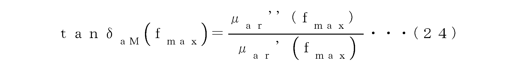
そして電磁波吸収体の比透磁率実部μar’と虚部μar’’の周波数分散を求め、虚部μar’’が極大値をもつ周波数を磁気損失最大周波数fmaxとした。そしてfmaxにおける比透磁率実部μar’(fmax)と虚部μar’’(fmax)を用いて、損失係数tanδaM(fmax)を下記(24)式にしたがって算出した。 The frequency dispersion of the relative permeability real part μ ar ' and imaginary part μ ar '' of the electromagnetic wave absorber was then determined, and the frequency at which the imaginary part μ ar '' had a maximum value was defined as the maximum magnetic loss frequency f max . The loss factor tan δ aM (f max ) was calculated according to the following formula (24) using the relative permeability real part μ ar ' (f max ) and imaginary part μ ar '' (f max ) at f max .
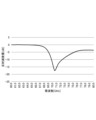
またサンプルの背後に厚さ1mmの金属板を設置し、電磁波の透過成分を十分に低減させた状態で反射特性を求めた。そして入射波強度と反射波強度の比から反射減衰量(率)RLを求めた。さらに反射減衰量の極大(吸収量の極大)が測定周波数内に存在するサンプルについて、反射減衰量が極大となる周波数を吸収周波数fRとし、fRにおける反射減衰量の絶対値を最大反射減衰量RLRとして求めた。またfRにおける電磁波(吸収電磁波)の大気中での波長λR、及び誘電体中での波長λR’を、下記(25)式及び(26)式にしたがって算出した。なお、下記(25)及び(26)式において、cは光速、εr’は誘電体の100MHzにおける複素比誘電率実部である。 A metal plate with a thickness of 1 mm was placed behind the sample, and the reflection characteristics were obtained in a state where the transmitted component of the electromagnetic wave was sufficiently reduced. The reflection loss (rate) RL was obtained from the ratio of the incident wave intensity to the reflected wave intensity. Furthermore, for samples in which the maximum reflection loss (maximum absorption amount) exists within the measurement frequency, the frequency at which the reflection loss is maximum was defined as the absorption frequency fR , and the absolute value of the reflection loss at fR was obtained as the maximum reflection loss RLR . The wavelength λR of the electromagnetic wave (absorbed electromagnetic wave) at fR in the atmosphere and the wavelength λR ' in the dielectric were calculated according to the following formulas (25) and (26). In the following formulas (25) and (26), c is the speed of light, and εr ' is the real part of the complex relative dielectric constant of the dielectric at 100 MHz.


(3)評価結果
例1~例4について誘電体の構成を表2にまとめて示す。また例1~4の電磁波吸収体の誘電率、透磁率及び伝送減衰量の周波数特性を図1~図9に示す。さらに電磁波吸収体の磁気特性及び吸収特性を表3及び表4にまとめて示す。
(3) Evaluation Results The dielectric structures of Examples 1 to 4 are summarized in Table 2. The frequency characteristics of the dielectric constant, magnetic permeability, and transmission attenuation of the electromagnetic wave absorbers of Examples 1 to 4 are shown in Figs. 1 to 9. Furthermore, the magnetic properties and absorption properties of the electromagnetic wave absorbers are summarized in Tables 3 and 4.
[例1]
表2に示されるように、例1の誘電体(焼結体)は、平均厚みが135μmであり、標準偏差が13μmであった。例1では、誘電体作製時の原料ペースト中のBaTiO3含有率が小さかった。そのため焼成時の厚み収縮が大きく、これが比較的大きい標準偏差につながったと考えられる。また表2に示されるように、例1の誘電体は、100MHzにおける比誘電率実部εr’が500程度と大きかった。このことから真空に対して大きな誘電応答を示すことが分かった。
[Example 1]
As shown in Table 2, the dielectric (sintered body) of Example 1 had an average thickness of 135 μm and a standard deviation of 13 μm. In Example 1, the BaTiO 3 content in the raw material paste during dielectric preparation was small. Therefore, the thickness shrinkage during firing was large, which is thought to have led to a relatively large standard deviation. Also, as shown in Table 2, the dielectric of Example 1 had a large relative dielectric constant real part ε r ' at 100 MHz of about 500. This shows that the dielectric exhibits a large dielectric response to vacuum.
例1の電磁波吸収体の比誘電率を図1に示す。誘電体(焼結体)を樹脂中に分散させて作製したたため、誘電体単体の場合と比べて誘電率が大きく低下していた。また誘電率に明確な共鳴挙動が見られなかった。 The relative dielectric constant of the electromagnetic wave absorber of Example 1 is shown in Figure 1. Because it was produced by dispersing the dielectric (sintered body) in the resin, the dielectric constant was significantly lower than in the case of a single dielectric. In addition, no clear resonance behavior was observed in the dielectric constant.
例1の電磁波吸収体の比透磁率を図2に示す。低周波側での透磁率実部はほぼ1であった。電磁波吸収体に含まれる誘電体は磁性元素を含んでいない。低周波側での透磁率実部の値は、磁性元素に基づく強磁性的な磁気秩序が生じていないことを裏付けている。一方で、強磁性的な磁気秩序が生じていないにもかかわらず、70GHz近傍で磁気的な共鳴が生じて、透磁率虚部が極大となっていた。透磁率虚部が最大となる周波数(磁気損失最大周波数)fmaxにおける比透磁率虚部μar’’は1.53、損失係数(tanδM)は1.79と非常に大きかった(表3)。強磁性的な磁気秩序が生じていないことから、誘電体の誘電率と厚みに依存するMie共鳴モードに起因する磁気損失が生じと考えられる。 The relative permeability of the electromagnetic wave absorber of Example 1 is shown in FIG. 2. The real part of the permeability on the low frequency side was almost 1. The dielectric contained in the electromagnetic wave absorber does not contain a magnetic element. The value of the real part of the permeability on the low frequency side confirms that a ferromagnetic magnetic order based on a magnetic element does not occur. On the other hand, even though a ferromagnetic magnetic order does not occur, magnetic resonance occurs near 70 GHz, and the imaginary part of the permeability becomes maximum. The imaginary part of the permeability μ ar ″ at the frequency fmax at which the imaginary part of the permeability becomes maximum (maximum magnetic loss frequency) was 1.53, and the loss factor (tan δ M ) was 1.79, which was very large (Table 3). Since a ferromagnetic magnetic order does not occur, it is considered that a magnetic loss occurs due to a Mie resonance mode that depends on the dielectric constant and thickness of the dielectric.
例1の電磁波吸収体の伝送減衰量(吸収特性)を図6に示す。70GHz近傍で伝送減衰量が極大となり、そのときのピーク値は-10dB超であった。誘電体の厚みを電磁波波長の1/2長程度にすることでMie共鳴が生じる。しかしながら強誘電体内ではその誘電率に起因した波長短縮が起こるため、表4に示すように厚みが波長と比べて十分小さい範囲で共鳴モードが生じることとなる。大半の強誘電体のGHz帯における比誘電率は100~10000の間にあるが、この場合、誘電体の厚みを測定波長の1/20~1/200程度にすることで上述した共鳴モードが生じると考えられる。本共鳴モード近傍では電磁波が焼結体内に効率よく侵入し吸収されると考えられる。 Figure 6 shows the transmission attenuation (absorption characteristics) of the electromagnetic wave absorber of Example 1. The transmission attenuation reaches a maximum near 70 GHz, with a peak value exceeding -10 dB. Mie resonance occurs when the thickness of the dielectric is about half the length of the electromagnetic wave wavelength. However, in the ferroelectric, wavelength shortening occurs due to its dielectric constant, so a resonance mode occurs in a range where the thickness is sufficiently smaller than the wavelength, as shown in Table 4. The relative dielectric constant of most ferroelectrics in the GHz band is between 100 and 10,000, but in this case, it is believed that the above-mentioned resonance mode will occur by making the thickness of the dielectric about 1/20 to 1/200 of the measured wavelength. It is believed that electromagnetic waves efficiently penetrate and are absorbed in the sintered body near this resonance mode.
[例2]
例2では、例1と同様にBaTiO3からなる誘電体(焼結体)を樹脂中に分散させて電磁波吸収体を作製した。誘電体作製時に3種類の異なる粒径(D50)をもつBaTiO3を混合することでペーストのBaTiO3含有率を高めた。その結果、表2に示すように、メタルマスク厚みと焼結体厚みの差が例1では15μmであるのに対し、例2では7μmと抑制されていた。また、収縮率低下に起因すると考えられる厚みの変動係数の低下も確認できた。加えて例1と比べて焼結体中のBaTiO3密度も向上していると考えられ、表2に示すような誘電体(焼結体)の誘電率増加も確認した。その結果、例2は例1と比べて波長短縮効果が強まり、表4に示すようにλR’と誘電体厚みの比が増大していた。
[Example 2]
In Example 2, an electromagnetic wave absorber was prepared by dispersing a dielectric (sintered body) made of BaTiO 3 in a resin in the same manner as in Example 1. The BaTiO 3 content of the paste was increased by mixing three types of BaTiO 3 with different particle sizes (D50) during dielectric preparation. As a result, as shown in Table 2, the difference between the metal mask thickness and the sintered body thickness was 15 μm in Example 1, whereas it was suppressed to 7 μm in Example 2. In addition, a decrease in the coefficient of variation of the thickness, which is thought to be due to a decrease in the shrinkage rate, was also confirmed. In addition, it is thought that the BaTiO 3 density in the sintered body is also improved compared to Example 1, and an increase in the dielectric constant of the dielectric (sintered body) was also confirmed as shown in Table 2. As a result, the wavelength shortening effect was strengthened in Example 2 compared to Example 1, and the ratio of λ R ' to the dielectric thickness was increased as shown in Table 4.
例2の電磁波吸収体の透磁率を図3に示す。例2では電磁波吸収体が備える誘電体の厚みが例1より薄いにも関わらず、例1と同程度の周波数で共鳴ピークが観察された。これは、誘電体の厚み低下による共鳴モードの高周波化が、誘電率の増加に依る共鳴モードの低周波化とほぼ打ち消しあったためと考えられる。 The magnetic permeability of the electromagnetic wave absorber of Example 2 is shown in Figure 3. In Example 2, even though the thickness of the dielectric material in the electromagnetic wave absorber is thinner than in Example 1, a resonance peak was observed at a frequency similar to that of Example 1. This is thought to be because the shift to higher frequencies in the resonance mode due to the reduced thickness of the dielectric material almost cancels out the shift to lower frequencies in the resonance mode due to the increased dielectric constant.
例2の電磁波吸収体の伝送減衰量(吸収特性)を図7に示す。透磁率の場合と同様に、吸収が極大となる周波数が例1とほぼ同じであることを確認した。 Figure 7 shows the transmission attenuation (absorption characteristics) of the electromagnetic wave absorber of Example 2. As with the magnetic permeability, it was confirmed that the frequency at which absorption was maximized was almost the same as in Example 1.
[例3]
例3では、例2と同じ配合組成でペーストを作製したものの、焼成は行わず乾燥のみ行って誘電体(成形体)を作製し、この成形体を樹脂中に分散して電磁波吸収体を作製した。誘電体(成形体)の平均厚みが例2と比べてわずかに増加していた。これは溶媒及び分散剤の一部が残留したためと考えられる。
[Example 3]
In Example 3, a paste was prepared with the same composition as in Example 2, but no firing was performed and only drying was performed to prepare a dielectric (molded body), and this molded body was dispersed in a resin to prepare an electromagnetic wave absorber. The average thickness of the dielectric (molded body) was slightly increased compared to Example 2. This is thought to be due to the fact that a part of the solvent and dispersant remained.
例3の電磁波吸収体の透磁率を図4に示す。例3の電磁波吸収体は成形体からなる誘電体を備えているが、焼結体からなる誘電体を備えた場合(例1及び例2)と同様の共鳴的挙動が見られた。しかしながら共鳴が起こる周波数が例2と比較して若干高周波側に移行していた。溶剤及び分散剤の一部が残留することで成形体全体の誘電率が低下し、波長短縮効果が弱まったためと考えられる。 The magnetic permeability of the electromagnetic wave absorber of Example 3 is shown in Figure 4. The electromagnetic wave absorber of Example 3 has a dielectric made of a molded body, and resonant behavior was observed similar to that of the cases with a dielectric made of a sintered body (Examples 1 and 2). However, the frequency at which resonance occurred was shifted slightly higher compared to Example 2. This is thought to be because some of the solvent and dispersant remained, lowering the dielectric constant of the entire molded body and weakening the wavelength shortening effect.
例3の電磁波吸収体の伝送減衰量(吸収特性)を図8に示す。磁気的な共鳴モードに対応して、焼結体を用いた場合(例1及び例2)と同様の吸収が起こることを確認した。また例3では、誘電体(成形体)をメタルマスクのパターンと同じく規則的に配置して電磁波吸収体を作製しているものの、ランダム配置した場合(例1及び例2)と類似の効果が得られている。個々の誘電体が電磁波吸収能をもつため、周囲の誘電体との配置態様が吸収能に与える影響が少ないためと考えられる。 Figure 8 shows the transmission attenuation (absorption characteristics) of the electromagnetic wave absorber of Example 3. It was confirmed that absorption occurred in the same way as in the case of using a sintered body (Examples 1 and 2) in response to the magnetic resonance mode. In Example 3, the dielectrics (molded bodies) were arranged in a regular pattern similar to the metal mask pattern to create the electromagnetic wave absorber, but an effect similar to that obtained when they were arranged randomly (Examples 1 and 2) was obtained. This is thought to be because each dielectric has electromagnetic wave absorption ability, and therefore the arrangement of the dielectrics relative to the surrounding dielectrics has little effect on absorption ability.
[例4]
例4では、BaTiO3のBaの一部をSrに置換した組成について誘電体(焼結体)を作製し、この誘電体を樹脂中に分散させて電磁波吸収体を作製した。この組成を有するペロブスカイト型化合物は室温においてリラクサー的な挙動を示すことが知られている。そのため誘電体(焼結体)は100MHzにおける誘電率が例1及び例2より高かった。
[Example 4]
In Example 4, a dielectric (sintered body) was prepared for a composition in which part of the Ba in BaTiO3 was replaced with Sr, and this dielectric was dispersed in a resin to prepare an electromagnetic wave absorber. It is known that perovskite compounds having this composition exhibit relaxor-like behavior at room temperature. Therefore, the dielectric constant of the dielectric (sintered body) at 100 MHz was higher than those of Examples 1 and 2.
例4の電磁波吸収体の透磁率を図5に示す。例1と比較すると誘電体の厚みが薄くなっているにも関わらず、ほぼ同じ周波数で共鳴的な挙動が見られた。これは、共鳴モードが生じる周波数に関して、誘電率増加による波長短縮及び周波数低減の効果と、誘電体厚み減少による周波数増加の効果が打ち消しあったためと考えられる。 Figure 5 shows the magnetic permeability of the electromagnetic wave absorber of Example 4. Although the dielectric thickness is thinner than in Example 1, resonant behavior was observed at approximately the same frequency. This is thought to be because, with regard to the frequency at which the resonant mode occurs, the effect of wavelength shortening and frequency reduction due to increased dielectric constant and the effect of frequency increase due to reduced dielectric thickness cancel each other out.
例4の電磁波吸収体の伝送減衰量を図9に示す。磁気的な共鳴モードに起因すると考えらえる吸収が確認された。 The transmission attenuation of the electromagnetic wave absorber of Example 4 is shown in Figure 9. Absorption thought to be due to a magnetic resonance mode was confirmed.

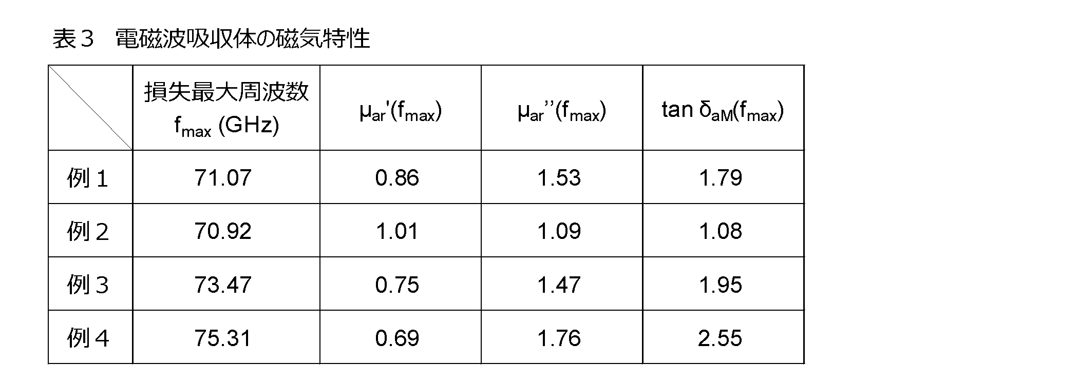

Claims (6)
前記電磁波吸収体は円板状誘電体を備え、
前記円板状誘電体は、100MHzにおける比誘電率実部εr’が30以上、且つ厚さT(単位:μm)に対する直径D(単位:μm)の比(D/T比)が3以上であり、
前記電磁波放射源が放射する電磁波の周波数f(単位:Hz)と、前記円板状誘電体の100MHzにおける比誘電率実部εr’及び厚さT(単位:μm)と、が、下記(1)及び(2)式(ただし、cは光速(3.0×1014μm/秒))を満足する、システム。

The electromagnetic wave absorber comprises a disk-shaped dielectric material,
the disk-shaped dielectric has a relative dielectric constant real part ε r ′ at 100 MHz of 30 or more and a ratio (D/T ratio) of a diameter D (unit: μm) to a thickness T (unit: μm) of 3 or more;
a frequency f (unit: Hz) of an electromagnetic wave radiated from the electromagnetic wave radiation source, a real part ε r ′ of a relative dielectric constant at 100 MHz and a thickness T (unit: μm) of the disk-shaped dielectric satisfy the following formulas (1) and (2) (where c is the speed of light (3.0×10 14 μm/sec)):
前記電磁波吸収体は円板状誘電体を備え、
前記円板状誘電体は、100MHzにおける比誘電率実部εr’が30以上、且つ厚さT(単位:μm)に対する直径D(単位:μm)の比(D/T比)が3以上であり、
前記電磁波の周波数f(単位:Hz)と、前記円板状誘電体の100MHzにおける比誘電率実部εr’及び厚さT(単位:μm)と、が、下記(1)及び(2)式(ただし、cは光速(3.0×1014μm/秒))を満足する、方法。

The electromagnetic wave absorber comprises a disk-shaped dielectric material,
the disk-shaped dielectric has a relative dielectric constant real part ε r ′ at 100 MHz of 30 or more and a ratio (D/T ratio) of a diameter D (unit: μm) to a thickness T (unit: μm) of 3 or more;
a frequency f (unit: Hz) of the electromagnetic wave, a real part ε r ′ of a relative dielectric constant at 100 MHz and a thickness T (unit: μm) of the disk-shaped dielectric satisfy the following formulas (1) and (2) (where c is the speed of light (3.0×10 14 μm/sec)):
6. The method according to claim 4, wherein the absolute value of the return loss of the electromagnetic wave absorber at the frequency f is 10 dB or more.
Priority Applications (2)
| Application Number | Priority Date | Filing Date | Title |
|---|---|---|---|
| JP2021028922A JP7608865B2 (en) | 2021-02-25 | 2021-02-25 | System equipped with electromagnetic wave absorber and method for absorbing electromagnetic waves using electromagnetic wave absorber |
| PCT/JP2022/007936 WO2022181774A1 (en) | 2021-02-25 | 2022-02-25 | System equipped with electromagnetic wave absorber, and electromagnetic wave absorbing method using electromagnetic wave absorber |
Applications Claiming Priority (1)
| Application Number | Priority Date | Filing Date | Title |
|---|---|---|---|
| JP2021028922A JP7608865B2 (en) | 2021-02-25 | 2021-02-25 | System equipped with electromagnetic wave absorber and method for absorbing electromagnetic waves using electromagnetic wave absorber |
Publications (2)
| Publication Number | Publication Date |
|---|---|
| JP2022130001A JP2022130001A (en) | 2022-09-06 |
| JP7608865B2 true JP7608865B2 (en) | 2025-01-07 |
Family
ID=83047538
Family Applications (1)
| Application Number | Title | Priority Date | Filing Date |
|---|---|---|---|
| JP2021028922A Active JP7608865B2 (en) | 2021-02-25 | 2021-02-25 | System equipped with electromagnetic wave absorber and method for absorbing electromagnetic waves using electromagnetic wave absorber |
Country Status (2)
| Country | Link |
|---|---|
| JP (1) | JP7608865B2 (en) |
| WO (1) | WO2022181774A1 (en) |
Families Citing this family (2)
| Publication number | Priority date | Publication date | Assignee | Title |
|---|---|---|---|---|
| JP2024166539A (en) * | 2023-05-19 | 2024-11-29 | 出光興産株式会社 | Radio wave absorber |
| WO2025206355A1 (en) * | 2024-03-29 | 2025-10-02 | 戸田工業株式会社 | Laminate including ferrite sintered plate |
Citations (2)
| Publication number | Priority date | Publication date | Assignee | Title |
|---|---|---|---|---|
| JP2004153135A (en) | 2002-10-31 | 2004-05-27 | Nichias Corp | Electromagnetic wave absorber |
| JP2013201359A (en) | 2012-03-26 | 2013-10-03 | Nitto Denko Corp | Electromagnetic wave absorber and method for manufacturing the same |
Family Cites Families (1)
| Publication number | Priority date | Publication date | Assignee | Title |
|---|---|---|---|---|
| JP5281504B2 (en) * | 2009-07-02 | 2013-09-04 | 株式会社ユポ・コーポレーション | EMI shield |
-
2021
- 2021-02-25 JP JP2021028922A patent/JP7608865B2/en active Active
-
2022
- 2022-02-25 WO PCT/JP2022/007936 patent/WO2022181774A1/en not_active Ceased
Patent Citations (2)
| Publication number | Priority date | Publication date | Assignee | Title |
|---|---|---|---|---|
| JP2004153135A (en) | 2002-10-31 | 2004-05-27 | Nichias Corp | Electromagnetic wave absorber |
| JP2013201359A (en) | 2012-03-26 | 2013-10-03 | Nitto Denko Corp | Electromagnetic wave absorber and method for manufacturing the same |
Also Published As
| Publication number | Publication date |
|---|---|
| JP2022130001A (en) | 2022-09-06 |
| WO2022181774A1 (en) | 2022-09-01 |
Similar Documents
| Publication | Publication Date | Title |
|---|---|---|
| Panwar et al. | Design of ferrite–graphene-based thin broadband radar wave absorber for stealth application | |
| Falcone et al. | Babinet principle applied to the design of metasurfaces and metamaterials | |
| Baskey et al. | Design of flexible hybrid nanocomposite structure based on frequency selective surface for wideband radar cross section reduction | |
| WO2004093155A2 (en) | Synthesis of metamaterial ferrites for rf applications using electromagnetic bandgap structures | |
| JP7608865B2 (en) | System equipped with electromagnetic wave absorber and method for absorbing electromagnetic waves using electromagnetic wave absorber | |
| KR101614716B1 (en) | Electromagnetic wave absorbation film and absorber with conductor pattern for absorbing near field noise | |
| Varghese et al. | Microwave materials for defense and aerospace applications | |
| Petrov et al. | Miniature antenna based on magnetoelectric composites | |
| Kim et al. | Active self-tuning metasurface with enhanced absorbing frequency range for suppression of high-power surface currents | |
| Wee et al. | Investigation of the characteristics of barium strontium titanate (BST) dielectric resonator ceramic loaded on array antennas | |
| Edries et al. | A tri-band metamaterial absorber for radar cross section reduction | |
| JP7600750B2 (en) | Electromagnetic wave absorber, system equipped with electromagnetic wave absorber, and method for absorbing electromagnetic waves using electromagnetic wave absorber | |
| Dey et al. | High-gain dielectric endfire antenna by forward scattering of dielectric spheres | |
| CN113015424B (en) | Superstructure millimeter wave absorbing plate and application thereof | |
| Yang et al. | Harmonic engineering of antennas with time-periodic substrate permittivity | |
| CN108183338A (en) | A kind of crown-shaped regulatable plasma Meta Materials broadband wave absorbing device | |
| Jacobsen et al. | Tunable water-based metasurface for anomalous wave reflection | |
| Dash et al. | Simulation and characterization of Mg-doped (BaTiO3–BaZrO3) ceramic metamaterial absorber for EMI shielding in Ku-band | |
| Saikia et al. | Synthesis and development of Fe3O4-expanded graphite embedded cement nanocomposites as excellent X-band microwave absorber | |
| WO2022158587A1 (en) | Method for manufacturing electromagnetic wave absorber | |
| De Sabata et al. | Design of Liquid Based Frequency Selective Surfaces Operating as Absorbers | |
| Garg et al. | Design of a compact band pass frequency selective surface for WLAN applications based on meander line topology | |
| Genovesi et al. | Miniaturized high impedance surfaces with angular stability by using zirconium tin titanate substrates and convoluted FSS elements | |
| Poplavko et al. | Microwave absorption mechanisms in dielectrics, semiconductors, ferrites, and metals | |
| CN116368004A (en) | Electromagnetic wave absorbing sheet |
Legal Events
| Date | Code | Title | Description |
|---|---|---|---|
| A621 | Written request for application examination |
Free format text: JAPANESE INTERMEDIATE CODE: A621 Effective date: 20230920 |
|
| TRDD | Decision of grant or rejection written | ||
| A01 | Written decision to grant a patent or to grant a registration (utility model) |
Free format text: JAPANESE INTERMEDIATE CODE: A01 Effective date: 20241119 |
|
| A61 | First payment of annual fees (during grant procedure) |
Free format text: JAPANESE INTERMEDIATE CODE: A61 Effective date: 20241202 |
|
| R150 | Certificate of patent or registration of utility model |
Ref document number: 7608865 Country of ref document: JP Free format text: JAPANESE INTERMEDIATE CODE: R150 |