JP7608801B2 - Adhesive for circuit connection, connection structure, and method for producing the connection structure - Google Patents
Adhesive for circuit connection, connection structure, and method for producing the connection structure Download PDFInfo
- Publication number
- JP7608801B2 JP7608801B2 JP2020198510A JP2020198510A JP7608801B2 JP 7608801 B2 JP7608801 B2 JP 7608801B2 JP 2020198510 A JP2020198510 A JP 2020198510A JP 2020198510 A JP2020198510 A JP 2020198510A JP 7608801 B2 JP7608801 B2 JP 7608801B2
- Authority
- JP
- Japan
- Prior art keywords
- adhesive
- circuit
- mass
- electrode
- circuit connection
- Prior art date
- Legal status (The legal status is an assumption and is not a legal conclusion. Google has not performed a legal analysis and makes no representation as to the accuracy of the status listed.)
- Active
Links
Images


Landscapes
- Adhesive Tapes (AREA)
- Adhesives Or Adhesive Processes (AREA)
- Conductive Materials (AREA)
Description
本発明は、回路接続用接着剤、接続構造体及び接続構造体の製造方法に関する。 The present invention relates to a circuit connection adhesive, a connection structure, and a method for manufacturing a connection structure.
従来、回路接続を行うために各種の接着材料が使用されている。例えば、液晶ディスプレイ(LCD)を駆動させる半導体が搭載されたTCP(Tape Carrier Package)又はCOF(Chip On Flex)とLCDパネル、あるいは、TCP又はCOFとプリント配線板とを電気的に接続するための接着材料(回路接続材料)として、接着剤中に導電粒子が分散された回路接続用接着剤が使用されている。 Conventionally, various adhesive materials have been used to connect circuits. For example, a circuit connection adhesive with conductive particles dispersed in it has been used as an adhesive material (circuit connection material) for electrically connecting a TCP (Tape Carrier Package) or COF (Chip On Flex) equipped with a semiconductor that drives a liquid crystal display (LCD) to an LCD panel, or a TCP or COF to a printed wiring board.
また、半導体をフェイスダウンで直接LCDパネル又はプリント配線板に実装する場合でも、従来のワイヤーボンディング法ではなく、薄膜化及び狭ピッチ接続に有利なフリップチップ実装が採用されており、ここでも、回路接続材料として、接着剤中に導電粒子が分散された回路接続用接着剤が用いられている(例えば、特許文献1参照)。 Even when semiconductors are mounted face-down directly on LCD panels or printed wiring boards, flip-chip mounting, which is advantageous for thin film and narrow pitch connections, is used instead of the conventional wire bonding method, and here too, a circuit connection adhesive in which conductive particles are dispersed is used as the circuit connection material (see, for example, Patent Document 1).
通常、回路接続用接着剤を用いた回路部材同士の接続は、回路部材間に当該回路接続用接着剤を介在させた状態で、加熱しながら回路部材同士を圧着(熱圧着)することにより行われている。熱圧着時の加熱温度は、回路部材の種類等により異なるが、例えば、回路部材として、プラスチック基板等の耐熱性に劣る基板、薄膜のガラス基板などを有する部材を用いる場合には、130~160℃程度の温度で熱圧着が行われる。 Normally, circuit components are connected together using a circuit connection adhesive by pressing the circuit components together while heating them (thermocompression bonding) with the circuit connection adhesive between them. The heating temperature during thermocompression bonding varies depending on the type of circuit component, but for example, when using circuit components that have substrates with poor heat resistance such as plastic substrates or thin glass substrates, thermocompression bonding is performed at a temperature of about 130 to 160°C.
近年、圧着箇所周辺の低耐熱性部材の破損の抑制、歩留まりの改善等の観点から、熱圧着時の温度の更なる低温化及び圧着時間の短時間化が求められており、例えば、130℃未満、5秒間以下の熱圧着により回路接続を行うことが求められている。しかしながら、本発明者らの検討の結果、従来の回路接続用接着剤を用いた場合、上記のような条件での熱圧着では、対向する電極間の接続抵抗値が上昇することが明らかとなった。 In recent years, from the viewpoints of preventing damage to low heat-resistant materials around the bonding points and improving yields, there has been a demand for lowering the temperature during thermocompression bonding and shortening the bonding time. For example, there is a demand for circuit connections to be made by thermocompression bonding at less than 130°C for 5 seconds or less. However, as a result of the inventors' investigations, it has become clear that when conventional circuit connection adhesives are used, thermocompression bonding under the above-mentioned conditions results in an increase in the connection resistance between opposing electrodes.
そこで、本発明は、低温短時間での熱圧着により、対向する電極間の接続抵抗が充分に低い接続構造体を得ることができる、回路接続用接着剤を提供することを主な目的する。 The main objective of the present invention is to provide an adhesive for circuit connections that can obtain a connection structure with sufficiently low connection resistance between opposing electrodes by thermocompression bonding at low temperatures in a short time.
本発明者らは、下記式(1)で表されるアニオンを有するオニウム塩が、脂環式エポキシ化合物と組み合わせた場合に特異的に低温硬化性の向上効果を示すことを見出し、本発明を完成させた。

すなわち、本発明の一側面は、以下の[1]に記載の回路接続用接着剤に関する。 That is, one aspect of the present invention relates to an adhesive for circuit connection as described in [1] below.
[1]カチオン重合性化合物と、熱カチオン重合開始剤と、導電粒子と、を含有し、前記カチオン重合性化合物が、脂環式エポキシ化合物を含み、前記熱カチオン重合開始剤が、下記式(1)で表されるアニオンを有するオニウム塩を含む、回路接続用接着剤。

上記側面の回路接続用接着剤によれば、低温短時間での熱圧着により、対向する電極間の接続抵抗が充分に低い接続構造体を得ることができる。このような効果が得られる理由は、明らかではないが、上記側面の回路接続用接着剤は、脂環式エポキシ化合物と上記式(1)で表されるアニオンを有するオニウム塩との組み合わせによって優れた低温硬化性を有するため、熱圧着時の導電粒子の過度な流動が抑制され、対向する電極間での導電粒子の捕捉性が向上し、結果として、接続抵抗の上昇が抑制されると推察される。 The circuit connection adhesive described above can be used to obtain a connection structure with sufficiently low connection resistance between opposing electrodes by thermocompression bonding at low temperatures in a short time. The reason for this effect is unclear, but it is presumed that the circuit connection adhesive described above has excellent low-temperature curing properties due to the combination of an alicyclic epoxy compound and an onium salt having an anion represented by formula (1) above, which suppresses excessive flow of conductive particles during thermocompression bonding, improves the capture of conductive particles between opposing electrodes, and as a result, suppresses an increase in connection resistance.
上記側面の回路接続用接着剤は、以下の[2]~[4]に記載の回路接続用接着剤であってよい。 The circuit connection adhesive on the side surface may be any of the circuit connection adhesives described in [2] to [4] below.
[2]前記熱カチオン重合開始剤が、前記オニウム塩として、スルホニウム塩及びアンモニウム塩からなる群より選択される少なくとも一種の化合物を含む、[1]に記載の回路接続用接着剤。 [2] The circuit connection adhesive described in [1], in which the thermal cationic polymerization initiator contains at least one compound selected from the group consisting of sulfonium salts and ammonium salts as the onium salt.
[3]フィルム状である、[1]又は[2]に記載の回路接続用接着剤。 [3] The circuit connection adhesive described in [1] or [2], which is in the form of a film.
[4]第一の接着剤層と、前記第一の接着剤層上に積層された第二の接着剤層と、を備え、前記第一の接着剤層が、前記カチオン重合性化合物と、前記熱カチオン重合開始剤と、前記導電粒子と、を含有する、[3]に記載の回路接続用接着剤。 [4] The circuit connection adhesive described in [3], comprising a first adhesive layer and a second adhesive layer laminated on the first adhesive layer, the first adhesive layer containing the cationic polymerizable compound, the thermal cationic polymerization initiator, and the conductive particles.
本発明の他の一側面は、以下の[5]に記載の接続構造体に関する。 Another aspect of the present invention relates to a connection structure as described in [5] below.
[5]第一の電極を有する第一の回路部材と、第二の電極を有する第二の回路部材と、前記第一の回路部材及び前記第二の回路部材の間に配置され、前記第一の電極及び前記第二の電極を互いに電気的に接続する回路接続部と、を備え、前記回路接続部が、[1]~[4]のいずれかに記載の回路接続用接着剤の硬化物を含む、接続構造体。 [5] A connection structure comprising a first circuit member having a first electrode, a second circuit member having a second electrode, and a circuit connection portion disposed between the first circuit member and the second circuit member and electrically connecting the first electrode and the second electrode to each other, the circuit connection portion including a cured product of the circuit connection adhesive described in any one of [1] to [4].
本発明の他の一側面は、以下の[6]に記載の接続構造体の製造方法に関する。 Another aspect of the present invention relates to a method for manufacturing a connection structure as described in [6] below.
[6]第一の電極を有する第一の回路部材と、第二の電極を有する第二の回路部材との間に、[1]~[4]のいずれかに記載の回路接続用接着剤を介在させ、前記第一の回路部材及び前記第二の回路部材を熱圧着して、前記第一の電極及び前記第二の電極を互いに電気的に接続する工程を備える、接続構造体の製造方法。 [6] A method for manufacturing a connection structure, comprising the steps of: interposing a circuit connection adhesive described in any one of [1] to [4] between a first circuit member having a first electrode and a second circuit member having a second electrode; and thermocompressing the first circuit member and the second circuit member to electrically connect the first electrode and the second electrode to each other.
本発明によれば、低温短時間での熱圧着により、対向する電極間の接続抵抗が充分に低い接続構造体を得ることができる、回路接続用接着剤を提供することができる。 The present invention provides an adhesive for circuit connections that can obtain a connection structure with sufficiently low connection resistance between opposing electrodes by thermocompression bonding at low temperatures in a short time.
本明細書において、「(メタ)アクリレート」とは、アクリレート、及び、それに対応するメタクリレートの少なくとも一方を意味する。「(メタ)アクリル」、「(メタ)アクリロイル」等の他の類似の表現においても同様である。また、「A又はB」とは、A及びBのどちらか一方を含んでいればよく、両方とも含んでいてもよい。また、「室温」とは、25℃を意味する。 In this specification, "(meth)acrylate" means at least one of acrylate and the corresponding methacrylate. The same applies to other similar expressions such as "(meth)acrylic" and "(meth)acryloyl". Furthermore, "A or B" means that either A or B is included, and may include both. Furthermore, "room temperature" means 25°C.
以下で例示する材料は、特に断らない限り、1種単独で用いてもよく、2種以上を組み合わせて用いてもよい。組成物中の各成分の含有量は、組成物中に各成分に該当する物質が複数存在する場合、特に断らない限り、組成物中に存在する当該複数の物質の合計量を意味する。また、「~」を用いて示された数値範囲は、「~」の前後に記載される数値をそれぞれ最小値及び最大値として含む範囲を示す。本明細書中に段階的に記載されている数値範囲において、ある段階の数値範囲の上限値又は下限値は、他の段階の数値範囲の上限値又は下限値に置き換えてもよい。また、本明細書中に記載されている数値範囲において、その数値範囲の上限値又は下限値は、実施例に示されている値に置き換えてもよい。また、個別に記載した上限値及び下限値は任意に組み合わせ可能である。 Unless otherwise specified, the materials exemplified below may be used alone or in combination of two or more. When a plurality of substances corresponding to each component are present in the composition, the content of each component in the composition means the total amount of the plurality of substances present in the composition, unless otherwise specified. Furthermore, a numerical range indicated using "~" indicates a range including the numerical values before and after "~" as the minimum and maximum values, respectively. In the numerical ranges described in stages in this specification, the upper or lower limit of a certain numerical range may be replaced by the upper or lower limit of a numerical range of another stage. Furthermore, in the numerical ranges described in this specification, the upper or lower limit of the numerical range may be replaced by the values shown in the examples. Furthermore, the upper and lower limits described individually can be combined arbitrarily.
以下、本発明の実施形態について説明するが、本発明はこれらの実施形態に何ら限定されるものではない。 The following describes embodiments of the present invention, but the present invention is not limited to these embodiments.
<回路接続用接着剤>
回路接続用接着剤は、カチオン重合性化合物(以下、「(a)成分」ともいう)と、熱カチオン重合開始剤(以下、「(b)成分」ともいう)と、導電粒子(以下、「(c)成分」ともいう)と、を含有する。この回路接続用接着剤において、カチオン重合性化合物は、脂環式エポキシ化合物を含み、熱カチオン重合開始剤は、下記式(1)で表されるアニオン(テトラキス[3,5-ビス(トリフルオロメチル)フェニル]ボレートアニオン)を有するオニウム塩(以下、「オニウム塩(1)」ともいう。)を含む。

The adhesive for circuit connection contains a cationic polymerizable compound (hereinafter also referred to as "component (a)"), a thermal cationic polymerization initiator (hereinafter also referred to as "component (b)"), and conductive particles (hereinafter also referred to as "component (c)"). In this adhesive for circuit connection, the cationic polymerizable compound includes an alicyclic epoxy compound, and the thermal cationic polymerization initiator includes an onium salt having an anion represented by the following formula (1) (tetrakis[3,5-bis(trifluoromethyl)phenyl]borate anion) (hereinafter also referred to as "onium salt (1)").
上記回路接続用接着剤は、例えば、第一の電極を有する第一の回路部材と、第二の電極を有する第二の回路部材との間に介在させ、第一の回路部材及び第二の回路部材を熱圧着して、第一の電極及び第二の電極を互いに電気的に接続するために用いられる。 The circuit connection adhesive is used, for example, to be interposed between a first circuit member having a first electrode and a second circuit member having a second electrode, and to electrically connect the first electrode and the second electrode to each other by thermocompression bonding the first circuit member and the second circuit member.
上記回路接続用接着剤によれば、回路接続時の熱圧着を低温短時間で行う場合において、対向する電極間の接続抵抗が充分に低い接続構造体を得ることができる。また、上記回路接続用接着剤によれば、接続信頼性に優れる回路接続構造体が得られる傾向がある。すなわち、上記回路接続用接着剤を用いて得られた接続構造体は、高温高湿雰囲気(例えば85℃、85%RH)に長期間さらされた場合でも剥離等の不具合を生じがたく、充分に低い接続抵抗を維持できる傾向がある。 When the above circuit connection adhesive is used, it is possible to obtain a connection structure in which the connection resistance between opposing electrodes is sufficiently low when thermocompression bonding during circuit connection is performed at a low temperature for a short period of time. Furthermore, the above circuit connection adhesive tends to provide a circuit connection structure with excellent connection reliability. That is, a connection structure obtained using the above circuit connection adhesive is unlikely to suffer from problems such as peeling even when exposed to a high-temperature, high-humidity atmosphere (e.g., 85°C, 85% RH) for a long period of time, and tends to be able to maintain a sufficiently low connection resistance.
回路接続用接着剤は、例えば、フィルム状である。以下では、フィルム状の回路接続用接着剤(回路接続用接着剤フィルム)を例に挙げて、回路接続用接着剤の詳細を説明する。 The circuit connection adhesive is, for example, in the form of a film. Below, the circuit connection adhesive is described in detail using a film-shaped circuit connection adhesive (circuit connection adhesive film) as an example.
回路接続用接着剤フィルムは、カチオン重合性化合物及び熱カチオン重合開始剤を含む接着剤成分と、接着剤成分中に分散された導電粒子とからなる、異方導電性の接着剤フィルムである。なお、本明細書では、回路接続用接着剤フィルムに含まれる導電粒子以外の成分を総称して接着剤成分と称する。また、「異方導電性」とは、加圧方向には導通し、非加圧方向では絶縁性を保つという意味である。 The circuit connection adhesive film is an anisotropically conductive adhesive film consisting of an adhesive component containing a cationic polymerizable compound and a thermal cationic polymerization initiator, and conductive particles dispersed in the adhesive component. In this specification, all components other than the conductive particles contained in the circuit connection adhesive film are collectively referred to as the adhesive component. In addition, "anisotropically conductive" means that it is conductive in the direction of pressure application and maintains insulation in the direction of no pressure application.
[(a)カチオン重合性化合物]
(a)成分は、例えば、熱によって熱カチオン重合開始剤(熱カチオン発生剤)が発生したカチオン種によって重合する化合物である。(a)成分は、少なくとも脂環式エポキシ化合物を含む。ここで、脂環式エポキシ化合物とは、脂環式エポキシ基を有する化合物をいう。
[(a) Cationic polymerizable compound]
The component (a) is, for example, a compound that undergoes polymerization by a cationic species generated by a thermal cationic polymerization initiator (thermal cationic generator) due to heat. The component (a) includes at least an alicyclic epoxy compound. Here, the alicyclic epoxy compound refers to a compound having an alicyclic epoxy group.
脂環式エポキシ化合物1分子中の脂環式エポキシ基の数は1つであっても2つ以上であってもよい。脂環式エポキシ化合物1分子中の脂環式エポキシ基の数が2つ以上である場合、硬化後の架橋密度が高くなる傾向がある。脂環式エポキシ化合物1分子中の脂環式エポキシ基の数は、例えば、6つ以下であってよい。 The number of alicyclic epoxy groups in one molecule of the alicyclic epoxy compound may be one or two or more. When the number of alicyclic epoxy groups in one molecule of the alicyclic epoxy compound is two or more, the crosslink density after curing tends to be high. The number of alicyclic epoxy groups in one molecule of the alicyclic epoxy compound may be, for example, six or less.
脂環式エポキシ化合物としては、シクロヘキセン、シクロペンテン等の脂環構造を有する化合物を酸化して得られる化合物(例えば、シクロヘキセンオキシド、シクロペンテンオキシド等を有する化合物)が挙げられる。 Alicyclic epoxy compounds include compounds obtained by oxidizing compounds having an alicyclic structure such as cyclohexene and cyclopentene (e.g., compounds having cyclohexene oxide, cyclopentene oxide, etc.).
脂環式エポキシ化合物の具体例としては、2-(3,4-エポキシシクロヘキシル-5,5-スピロ-3,4-エポキシ)シクロヘキサン-メタジオキサン、3,4-エポキシ-1-メチルシクロヘキシル-3,4-エポキシ-1-メチルヘキサンカルボキシレート、3,4-エポキシ-3-メチルシクロヘキシルメチル-3,4-エポキシ-3-メチルシクロヘキサンカルボキシレート、3,4-エポキシ-5-メチルシクロヘキシルメチル-3,4-エポキシ-5-メチルシクロヘキサンカルボキシレート、3,4-エポキシ-6-メチルシクロエキシルカルボキシレート、3,4-エポキシシクロヘキシルメチル-3,4-エポキシシクロヘキサンカルボキシレート、6-メチル-3,4-エポキシシクロヘキシルメチル-6-メチル-3,4-エポキシシクロヘキサンカルボキシレート、エチレンビス(3,4-エポキシシクロヘキサンカルボキシレート)、ジシクロペンタジエンジエポキシド、ビス(3,4-エポキシシクロヘキシルメチル)アジペート、メチレンビス(3,4-エポキシシクロヘキサン)、3,4-エポキシシクロヘキシルメチル(メタ)アクリレート、(3,3’、4,4’-ジエポキシ)ビシクロヘキシル、水添ビスフェノールA型エポキシ樹脂、水添ビスフェノールF型エポキシ樹脂等が挙げられる。 Specific examples of alicyclic epoxy compounds include 2-(3,4-epoxycyclohexyl-5,5-spiro-3,4-epoxy)cyclohexane-metadioxane, 3,4-epoxy-1-methylcyclohexyl-3,4-epoxy-1-methylhexanecarboxylate, 3,4-epoxy-3-methylcyclohexylmethyl-3,4-epoxy-3-methylcyclohexanecarboxylate, 3,4-epoxy-5-methylcyclohexylmethyl-3,4-epoxy-5-methylcyclohexanecarboxylate, 3,4-epoxy-6-methylcyclohexylcarboxylate, 3,4-epoxycyclohexylmethyl- Examples include 3,4-epoxycyclohexane carboxylate, 6-methyl-3,4-epoxycyclohexylmethyl-6-methyl-3,4-epoxycyclohexane carboxylate, ethylene bis(3,4-epoxycyclohexane carboxylate), dicyclopentadiene diepoxide, bis(3,4-epoxycyclohexylmethyl)adipate, methylene bis(3,4-epoxycyclohexane), 3,4-epoxycyclohexylmethyl(meth)acrylate, (3,3',4,4'-diepoxy)bicyclohexyl, hydrogenated bisphenol A type epoxy resin, hydrogenated bisphenol F type epoxy resin, etc.
脂環式エポキシ化合物の市販品としては、例えば、EHPE3150、EHPE3150CE、CEL(セロキサイド)8010、CEL(セロキサイド)2021P、CEL(セロキサイド)2081(商品名、株式会社ダイセル製)等が挙げられる。 Commercially available alicyclic epoxy compounds include, for example, EHPE3150, EHPE3150CE, CEL (celloxide) 8010, CEL (celloxide) 2021P, and CEL (celloxide) 2081 (trade names, manufactured by Daicel Corporation).
脂環式エポキシ化合物は1種を単独で用いてよく、複数種を組み合わせて用いてもよい。 The alicyclic epoxy compounds may be used alone or in combination.
脂環式エポキシ化合物のエポキシ当量は、例えば、接着強度の観点から、100~300g/eqであってよい。エポキシ当量は、JIS K 7236に準拠して決定される。 The epoxy equivalent of the alicyclic epoxy compound may be, for example, 100 to 300 g/eq from the viewpoint of adhesive strength. The epoxy equivalent is determined in accordance with JIS K 7236.
脂環式エポキシ化合物の含有量は、回路接続用接着剤の硬化性を担保する観点から、接着剤成分の合計量を基準として、10質量%以上、15質量%以上又は20質量%以上であってよい。脂環式エポキシ化合物の含有量は、回路接続用接着剤のフィルム形成性を担保する観点から、接着剤成分の合計量を基準として、60質量%以下、55質量%以下又は50質量%以下であってよい。これらの観点から、脂環式エポキシ化合物の含有量は、接着剤成分の合計量を基準として、10~60質量%、15~55質量%又は20~50質量%であってよい。 The content of the alicyclic epoxy compound may be 10% by mass or more, 15% by mass or more, or 20% by mass or more, based on the total amount of the adhesive components, from the viewpoint of ensuring the curability of the circuit connection adhesive. The content of the alicyclic epoxy compound may be 60% by mass or less, 55% by mass or less, or 50% by mass or less, based on the total amount of the adhesive components, from the viewpoint of ensuring the film formability of the circuit connection adhesive. From these viewpoints, the content of the alicyclic epoxy compound may be 10 to 60% by mass, 15 to 55% by mass, or 20 to 50% by mass, based on the total amount of the adhesive components.
(a)成分は、脂環式エポキシ化合物以外のカチオン重合性化合物を更に含んでいてよい。脂環式エポキシ化合物以外のカチオン重合性化合物としては、例えば、脂環式エポキシ化合物以外のエポキシ化合物、オキセタン化合物等の環状エーテル基を有する化合物が挙げられる。これらの中でも、(a)成分がオキセタン化合物を更に含む場合、架橋密度が高くなり、接続抵抗の低減効果がより顕著に得られる傾向があり、また、より優れた接続信頼性が得られる傾向がある。 Component (a) may further contain a cationic polymerizable compound other than an alicyclic epoxy compound. Examples of cationic polymerizable compounds other than an alicyclic epoxy compound include epoxy compounds other than alicyclic epoxy compounds, and compounds having a cyclic ether group such as oxetane compounds. Among these, when component (a) further contains an oxetane compound, the crosslink density tends to be high, the effect of reducing the connection resistance tends to be more significant, and better connection reliability tends to be obtained.
オキセタン化合物は、オキセタニル基を有する化合物である。オキセタン化合物1分子中のオキセタニル基の数は1つであっても2つ以上であってもよい。オキセタン化合物1分子中のオキセタニル基の数が2つ以上である場合、硬化後の架橋密度がより一層高くなりやすく、また、脂環式エポキシ化合物との組み合わせによる相乗効果が得られやすくなる。オキセタン化合物1分子中のオキセタニル基の数は、例えば、6つ以下であってよい。 The oxetane compound is a compound having an oxetanyl group. The number of oxetanyl groups in one molecule of the oxetane compound may be one or two or more. When the number of oxetanyl groups in one molecule of the oxetane compound is two or more, the crosslink density after curing tends to be higher, and a synergistic effect is more easily obtained by combining with an alicyclic epoxy compound. The number of oxetanyl groups in one molecule of the oxetane compound may be, for example, six or less.
オキセタン化合物としては、例えば、2-エチルヘキシルオキセタン、3-ヒドロキシメチル-3-メチルオキセタン、3-ヒドロキシメチル-3-エチルオキセタン、3-ヒドロキシメチル-3-プロピルオキセタン、3-ヒドロキシメチル-3-ノルマルブチルオキセタン、3-ヒドロキシメチル-3-フェニルオキセタン、3-ヒドロキシメチル-3-ベンジルオキセタン、3-ヒドロキシエチル-3-メチルオキセタン、3-ヒドロキシエチル-3-エチルオキセタン、3-ヒドロキシエチル-3-プロピルオキセタン、3-ヒドロキシエチル-3-フェニルオキセタン、3-ヒドロキシプロピル-3-メチルオキセタン、3-ヒドロキシプロピル-3-エチルオキセタン、3-ヒドロキシプロピル-3-プロピルオキセタン、3-ヒドロキシプロピル-3-フェニルオキセタン、3-ヒドロキシブチル-3-メチルオキセタン、4,4’-ビス[(3-エチル-3-オキセタニル)メトキシメチル]ビフェニル等が挙げられる。 Examples of oxetane compounds include 2-ethylhexyloxetane, 3-hydroxymethyl-3-methyloxetane, 3-hydroxymethyl-3-ethyloxetane, 3-hydroxymethyl-3-propyloxetane, 3-hydroxymethyl-3-n-butyloxetane, 3-hydroxymethyl-3-phenyloxetane, 3-hydroxymethyl-3-benzyloxetane, 3-hydroxyethyl-3-methyloxetane, and 3-hydroxyethyl-3-ethyloxetane. Examples include oxetane, 3-hydroxyethyl-3-propyloxetane, 3-hydroxyethyl-3-phenyloxetane, 3-hydroxypropyl-3-methyloxetane, 3-hydroxypropyl-3-ethyloxetane, 3-hydroxypropyl-3-propyloxetane, 3-hydroxypropyl-3-phenyloxetane, 3-hydroxybutyl-3-methyloxetane, and 4,4'-bis[(3-ethyl-3-oxetanyl)methoxymethyl]biphenyl.
オキセタン化合物の市販品としては、例えば、ETERNACOLL OXBP(商品名、4,4’-ビス[(3-エチル-3-オキセタニル)メトキシメチル]ビフェニル、宇部興産株式会社製)、OXSQ、OXT-121、OXT-221、OXT-101、OXT-212(商品名、東亜合成株式会社製)等が挙げられる。 Commercially available oxetane compounds include, for example, ETERNACOLL OXBP (product name, 4,4'-bis[(3-ethyl-3-oxetanyl)methoxymethyl]biphenyl, manufactured by Ube Industries, Ltd.), OXSQ, OXT-121, OXT-221, OXT-101, and OXT-212 (product names, manufactured by Toagosei Co., Ltd.).
オキセタン化合物は1種を単独で用いてよく、複数種を組み合わせて用いてもよい。 The oxetane compounds may be used alone or in combination.
(a)成分がオキセタン化合物を更に含む場合、脂環式エポキシ化合物の含有量に対するオキセタン化合物の含有量の質量比率(オキセタン化合物の含有量/脂環式エポキシ化合物の含有量)は、オキセタン化合物の反応性を向上させ、脂環式エポキシ化合物との組み合わせによる相乗効果が得られやすくなる観点から、0.2以上、0.5以上、1.0以上又は1.5以上であってよく、5.0以下、4.0以下、3.0以下又は2.5以下であってよく、0.2~5.0、0.5~4.0、1.0~3.0又は1.5~2.5であってよい。 When component (a) further contains an oxetane compound, the mass ratio of the content of the oxetane compound to the content of the alicyclic epoxy compound (content of oxetane compound/content of alicyclic epoxy compound) may be 0.2 or more, 0.5 or more, 1.0 or more, or 1.5 or more, and may be 5.0 or less, 4.0 or less, 3.0 or less, or 2.5 or less, or may be 0.2 to 5.0, 0.5 to 4.0, 1.0 to 3.0, or 1.5 to 2.5, from the viewpoint of improving the reactivity of the oxetane compound and making it easier to obtain a synergistic effect by combining it with the alicyclic epoxy compound.
(a)成分の含有量は、回路接続用接着剤の硬化性を担保する観点から、接着剤成分の合計量を基準として、10質量%以上、15質量%以上、20質量%以上であってよい。(a)成分の含有量は、回路接続用接着剤のフィルム形成性を担保する観点から、接着剤成分の合計量を基準として、50質量%以下、40質量%以下又は30質量%以下であってよい。これらの観点から、(a)成分の含有量は、接着剤成分の合計量を基準として、10~50質量%、15~40質量%又は20~30質量%であってよい。 The content of component (a) may be 10% by mass or more, 15% by mass or more, or 20% by mass or more based on the total amount of the adhesive components, from the viewpoint of ensuring the curability of the circuit connection adhesive. The content of component (a) may be 50% by mass or less, 40% by mass or less, or 30% by mass or less based on the total amount of the adhesive components, from the viewpoint of ensuring the film formability of the circuit connection adhesive. From these viewpoints, the content of component (a) may be 10 to 50% by mass, 15 to 40% by mass, or 20 to 30% by mass, based on the total amount of the adhesive components.
[(b)熱カチオン重合開始剤]
(b)成分は、加熱によりカチオン種(酸等)を発生して重合を開始させる化合物であり、例えば、カチオンとアニオンとから構成される塩化合物である。(b)成分は、少なくともオニウム塩(1)を含む。
[(b) Thermal cationic polymerization initiator]
The component (b) is a compound that generates a cationic species (such as an acid) upon heating to initiate polymerization, and is, for example, a salt compound composed of a cation and an anion. The component (b) contains at least an onium salt (1).
オニウム塩(1)が有するカチオンは特に限定されない。オニウム塩(1)は、例えば、スルホニウム塩、ホスホニウム塩、アンモニウム塩、ジアゾニウム塩又はヨードニウム塩であってよい。これらの中でも、スルホニウム塩及びアンモニウム塩からなる群より選択される少なくとも一種を用いる場合、より低い接続抵抗が得られる傾向がある。かかる傾向は、アンモニウム塩(特にアニリニウム塩)を用いる場合に強くなる。 The cation contained in the onium salt (1) is not particularly limited. The onium salt (1) may be, for example, a sulfonium salt, a phosphonium salt, an ammonium salt, a diazonium salt, or an iodonium salt. Among these, when at least one selected from the group consisting of a sulfonium salt and an ammonium salt is used, a lower connection resistance tends to be obtained. This tendency becomes stronger when an ammonium salt (particularly anilinium salt) is used.
アニリニウム塩としては、例えば、N-アルキルアニリニウム塩、N,N-ジアルキルアニリニウム塩、N,N,N-トリアルキルアニリニウム塩、N-ベンジルアニリニウム塩(N-アルキル-N-ベンジルアニリニウム塩及びN,N-ジアルキル-N-ベンジルアニリニウム塩を含む)等が挙げられる。これらのアニリニウム塩において、窒素原子に結合する炭化水素基(アルキル及びベンジル)は、置換基を有するものであってよい。 Examples of anilinium salts include N-alkylanilinium salts, N,N-dialkylanilinium salts, N,N,N-trialkylanilinium salts, and N-benzylanilinium salts (including N-alkyl-N-benzylanilinium salts and N,N-dialkyl-N-benzylanilinium salts). In these anilinium salts, the hydrocarbon group (alkyl and benzyl) bonded to the nitrogen atom may have a substituent.
オニウム塩(1)は、低温短時間での熱圧着時における接続抵抗の低減効果を向上させる観点から、下記式(2)で表されるカチオン(N-ベンジルアニリニウムイオン)を有する塩であってよい。

式(2)中、R1、R2、R3、R8、R9及びR10は、それぞれ独立して、水素原子、ハロゲン原子、炭素数1~3のアルキル基、炭素数1~12のアルコキシ基、ニトロ基、アミノ基、アルキルアミノ基、シアノ基、アルコキシカルボニル基、又はカルボニル基を示し、R4及びR5は、それぞれ独立して、水素原子、炭素数1~3のアルキル基、又はハロゲン原子を示し、R6及びR7は、それぞれ独立して、ハロゲン原子、炭素数1~3のアルキル基を示す。 In formula (2), R 1 , R 2 , R 3 , R 8 , R 9 and R 10 each independently represent a hydrogen atom, a halogen atom, an alkyl group having 1 to 3 carbon atoms, an alkoxy group having 1 to 12 carbon atoms, a nitro group, an amino group, an alkylamino group, a cyano group, an alkoxycarbonyl group, or a carbonyl group; R 4 and R 5 each independently represent a hydrogen atom, an alkyl group having 1 to 3 carbon atoms, or a halogen atom; and R 6 and R 7 each independently represent a halogen atom or an alkyl group having 1 to 3 carbon atoms.
上記式(2)で表されるカチオンの具体例としては、N-ベンジル-N,N-ジメチルアニリニウムイオン、N-(4-ニトロベンジル)-N,N-ジメチルアニリニウムイオン、N-(4-メトキシベンジル)-N,N-ジメチルアニリニウムイオン、N-(α-フェニルベンジル)-N,N-ジメチルアニリニウムイオン、N-(α-メチルベンジル)-N,N-ジメチルアニリニウムイオン、N-(1-ナフチルメチル)-N,N-ジメチルアニリニウムイオン、N-シンナミル-N,N-ジメチルアニリニウムイオン等が挙げられる。 Specific examples of the cation represented by the above formula (2) include N-benzyl-N,N-dimethylanilinium ion, N-(4-nitrobenzyl)-N,N-dimethylanilinium ion, N-(4-methoxybenzyl)-N,N-dimethylanilinium ion, N-(α-phenylbenzyl)-N,N-dimethylanilinium ion, N-(α-methylbenzyl)-N,N-dimethylanilinium ion, N-(1-naphthylmethyl)-N,N-dimethylanilinium ion, and N-cinnamyl-N,N-dimethylanilinium ion.
オニウム塩(1)は、例えば、上記式(1)で表されるアニオンとナトリウムイオンとの塩と、オニウム塩(1)の対カチオンとなるイオンとヨウ化物イオンとの塩と、を用意し、これらを混合すること等により調製することができる。 The onium salt (1) can be prepared, for example, by preparing a salt of the anion represented by the above formula (1) and a sodium ion, and a salt of an ion that serves as a counter cation of the onium salt (1) and an iodide ion, and mixing these together.
オニウム塩(1)は1種を単独で用いてよく、複数種を組み合わせて用いてもよい。 The onium salt (1) may be used alone or in combination with multiple types.
オニウム塩化物(1)の含有量は、低温短時間での熱圧着時における接続抵抗の低減効果を向上させる観点から、脂環式エポキシ化合物100質量部に対して、10質量部以上、15質量部以上又は20質量部以上であってよい。オニウム塩化物(1)の含有量は、低温短時間での熱圧着時における接続抵抗の低減効果を向上させる観点から、脂環式エポキシ化合物100質量部に対して、45質量部以下、40質量部以下又は35質量部以下であってよい。これらの観点から、オニウム塩化物(1)の含有量は、脂環式エポキシ化合物100質量部に対して、10~45質量部、10~40質量部、15~45質量部、15~40質量部又は20~35質量部であってよい。 The content of onium chloride (1) may be 10 parts by mass or more, 15 parts by mass or more, or 20 parts by mass or more, relative to 100 parts by mass of the alicyclic epoxy compound, from the viewpoint of improving the effect of reducing the connection resistance during thermocompression bonding at low temperature in a short time. The content of onium chloride (1) may be 45 parts by mass or less, 40 parts by mass or less, or 35 parts by mass or less, relative to 100 parts by mass of the alicyclic epoxy compound, from the viewpoint of improving the effect of reducing the connection resistance during thermocompression bonding at low temperature in a short time. From these viewpoints, the content of onium chloride (1) may be 10 to 45 parts by mass, 10 to 40 parts by mass, 15 to 45 parts by mass, 15 to 40 parts by mass, or 20 to 35 parts by mass, relative to 100 parts by mass of the alicyclic epoxy compound.
オニウム塩化物(1)の含有量は、低温短時間での熱圧着時における接続抵抗の低減効果を向上させる観点から、接着剤成分の合計量を基準として、0.5質量%以上、1.0質量%以上又は3.0質量%以上であってよい。オニウム塩化物(1)の含有量は、低温短時間での熱圧着時における接続抵抗の低減効果を向上させる観点から、接着剤成分の合計量を基準として、20質量%以下、15質量%以下又は10質量%以下であってよい。これらの観点から、オニウム塩化物(1)の含有量は、接着剤成分の合計量を基準として、0.5~20質量%、1.0~15質量%又は3.0~10質量%であってよい。 The content of onium chloride (1) may be 0.5% by mass or more, 1.0% by mass or more, or 3.0% by mass or more based on the total amount of adhesive components, from the viewpoint of improving the effect of reducing connection resistance during thermocompression bonding at low temperatures in a short time. The content of onium chloride (1) may be 20% by mass or less, 15% by mass or less, or 10% by mass or less based on the total amount of adhesive components, from the viewpoint of improving the effect of reducing connection resistance during thermocompression bonding at low temperatures in a short time. From these viewpoints, the content of onium chloride (1) may be 0.5 to 20% by mass, 1.0 to 15% by mass, or 3.0 to 10% by mass based on the total amount of adhesive components.
(b)成分は、オニウム塩化物(1)以外の熱カチオン重合開始剤を含んでいてもよい。(b)成分の全質量を基準とするオニウム塩化物(1)の含有量は、例えば、90質量%以上であってよく、100質量%であってもよい。 The (b) component may contain a thermal cationic polymerization initiator other than the onium chloride (1). The content of the onium chloride (1) based on the total mass of the (b) component may be, for example, 90% by mass or more, or may be 100% by mass.
(b)成分の含有量は、低温短時間での熱圧着時における接続抵抗の低減効果を向上させる観点から、接着剤成分の合計量を基準として、0.5質量%以上、1.0質量%以上又は3.0質量%以上であってよい。(b)成分の含有量は、低温短時間での熱圧着時における接続抵抗の低減効果を向上させる観点から、接着剤成分の合計量を基準として、20質量%以下、15質量%以下又は10質量%以下であってよい。これらの観点から、(b)成分の含有量は、接着剤成分の合計量を基準として、0.5~20質量%、1.0~15質量%又は3.0~10質量%であってよい。 The content of the (b) component may be 0.5 mass% or more, 1.0 mass% or more, or 3.0 mass% or more based on the total amount of the adhesive components, from the viewpoint of improving the effect of reducing the connection resistance during thermocompression bonding at low temperatures in a short time. The content of the (b) component may be 20 mass% or less, 15 mass% or less, or 10 mass% or less based on the total amount of the adhesive components, from the viewpoint of improving the effect of reducing the connection resistance during thermocompression bonding at low temperatures in a short time. From these viewpoints, the content of the (b) component may be 0.5 to 20 mass%, 1.0 to 15 mass%, or 3.0 to 10 mass% based on the total amount of the adhesive components.
[(c)導電粒子]
(c)成分としては、導電性を有する粒子であれば特に制限されず、金、銀、パラジウム、ニッケル、銅、はんだ等の金属で構成された金属粒子、導電性カーボンで構成された導電性カーボン粒子などであってよい。(c)成分は、非導電性のガラス、セラミック、プラスチック(ポリスチレン等)などを含む核と、上記金属又は導電性カーボンを含み、核を被覆する被覆層とを備える被覆導電粒子であってもよい。これらの中でも、(c)成分が、熱溶融性の金属で形成された金属粒子及び被覆導電粒子からなる群より選ばれる少なくとも一種を含む場合(特に被覆導電粒子を含む場合)、加熱及び/又は加圧することにより変形させることが容易となり、電極同士を電気的に接続する際に、電極と導電粒子との接触面積を増加させ、電極間の導電性をより向上させることができる。
[(c) Conductive Particles]
The (c) component is not particularly limited as long as it is a conductive particle, and may be a metal particle composed of a metal such as gold, silver, palladium, nickel, copper, or solder, or a conductive carbon particle composed of conductive carbon. The (c) component may be a coated conductive particle having a core containing non-conductive glass, ceramic, plastic (polystyrene, etc.), and a coating layer containing the above metal or conductive carbon and coating the core. Among these, when the (c) component contains at least one selected from the group consisting of metal particles and coated conductive particles formed of a heat-fusible metal (especially when it contains coated conductive particles), it becomes easy to deform by heating and/or pressing, and when the electrodes are electrically connected to each other, the contact area between the electrodes and the conductive particles can be increased, and the conductivity between the electrodes can be further improved.
(c)成分の平均粒子径は、分散性及び導電性に優れる観点から、1.0μm以上、2.0μm以上又は2.5μm以上であってよい。(c)成分の平均粒子径は、隣り合う電極間の絶縁性を確保する観点から、6.0μm以下、5.5μm以下又は5.0μm以下であってよい。これらの観点から、(c)成分の平均粒子径は、1.0~6.0μm、2.0~5.5μm又は2.5~5.0μmであってよい。なお、回路接続用接着剤に含まれる導電粒子300個について、走査型電子顕微鏡(SEM)を用いた観察により粒子径の測定を行い、得られた粒子径の平均値を(c)成分の平均粒子径とする。導電粒子が球形ではない場合、導電粒子の粒子径は、SEMによる観察画像における導電粒子に外接する円の直径とする。 The average particle diameter of the (c) component may be 1.0 μm or more, 2.0 μm or more, or 2.5 μm or more, from the viewpoint of excellent dispersibility and conductivity. The average particle diameter of the (c) component may be 6.0 μm or less, 5.5 μm or less, or 5.0 μm or less, from the viewpoint of ensuring insulation between adjacent electrodes. From these viewpoints, the average particle diameter of the (c) component may be 1.0 to 6.0 μm, 2.0 to 5.5 μm, or 2.5 to 5.0 μm. The particle diameters of 300 conductive particles contained in the circuit connection adhesive are measured by observation using a scanning electron microscope (SEM), and the average value of the particle diameters obtained is taken as the average particle diameter of the (c) component. If the conductive particles are not spherical, the particle diameter of the conductive particles is taken as the diameter of a circle circumscribing the conductive particles in the image observed by SEM.
(c)成分は、回路接続用接着剤フィルム中で均一に分散されていてよい。回路接続用接着剤フィルムにおける(c)成分の粒子密度は、安定した接続抵抗が得られる観点から、100個/mm2以上、1000個/mm2以上又は3000個/mm2以上であってよい。回路接続用接着剤フィルムにおける(c)成分の粒子密度は、隣り合う電極間の絶縁性を確保する観点から、100000個/mm2以下、50000個/mm2以下又は30000個/mm2以下であってよい。これらの観点から、回路接続用接着剤フィルムにおける(c)成分の粒子密度は、100~100000個/mm2、1000~50000個/mm2又は3000~30000個/mm2であってよい。 The (c) component may be uniformly dispersed in the circuit connection adhesive film. The particle density of the (c) component in the circuit connection adhesive film may be 100 particles/mm2 or more , 1000 particles/mm2 or more, or 3000 particles/mm2 or more , from the viewpoint of obtaining a stable connection resistance. The particle density of the (c) component in the circuit connection adhesive film may be 100,000 particles/mm2 or less , 50,000 particles/mm2 or less , or 30,000 particles/mm2 or less , from the viewpoint of ensuring insulation between adjacent electrodes. From these viewpoints, the particle density of the (c) component in the circuit connection adhesive film may be 100 to 100,000 particles/ mm2 , 1000 to 50,000 particles/ mm2 , or 3000 to 30,000 particles/ mm2 .
(c)成分の含有量は、安定した接続抵抗が得られる観点から、回路接続用接着剤の全質量を基準として、10質量%以上、20質量%以上又は30質量%以上であってよい。(c)成分の含有量は、隣り合う電極間の絶縁性を確保する観点から、回路接続用接着剤の全質量を基準として、60質量%以下、50質量%以下又は40質量%以下であってよい。 The content of component (c) may be 10% by mass or more, 20% by mass or more, or 30% by mass or more, based on the total mass of the circuit connection adhesive, from the viewpoint of obtaining a stable connection resistance. The content of component (c) may be 60% by mass or less, 50% by mass or less, or 40% by mass or less, based on the total mass of the circuit connection adhesive, from the viewpoint of ensuring insulation between adjacent electrodes.
[その他の成分]
回路接続用接着剤フィルムは、上述した成分以外の成分(その他の成分)を更に含有してもよい。その他の成分としては、例えば、熱可塑性樹脂、カップリング剤、充填材等が挙げられる。これらの成分は、接着剤成分に含まれる。
[Other ingredients]
The adhesive film for circuit connection may further contain components (other components) other than the components described above. Examples of the other components include thermoplastic resins, coupling agents, fillers, etc. These components are included in the adhesive component.
-熱可塑性樹脂
熱可塑性樹脂は、回路接続用接着剤のフィルム形成性の向上に寄与する。熱可塑性樹脂としては、フェノキシ樹脂、ポリエステル樹脂、ポリアミド樹脂、ポリウレタン樹脂、ポリエステルウレタン樹脂、アクリルゴム、エポキシ樹脂(25℃で固形)等が挙げられる。これらは、一種を単独で用いてもよく、二種以上を組み合わせて用いてもよい。
Thermoplastic resins contribute to improving the film-forming properties of the circuit-connecting adhesive. Examples of thermoplastic resins include phenoxy resins, polyester resins, polyamide resins, polyurethane resins, polyester urethane resins, acrylic rubbers, and epoxy resins (solid at 25°C). These may be used alone or in combination of two or more.
熱可塑性樹脂の重量平均分子量(Mw)は、例えば、5000~200000であってよく、10000~100000であってよく、20000~80000であってよく、40000~60000であってよい。なお、熱可塑性樹脂の重量平均分子量は、ゲルパーミエーションクロマトグラフィー(GPC)で測定し、標準ポリスチレンによる検量線を用いて換算した値を意味する。 The weight average molecular weight (Mw) of the thermoplastic resin may be, for example, 5,000 to 200,000, 10,000 to 100,000, 20,000 to 80,000, or 40,000 to 60,000. The weight average molecular weight of the thermoplastic resin refers to a value measured by gel permeation chromatography (GPC) and converted using a calibration curve based on standard polystyrene.
熱可塑性樹脂の含有量は、接着剤成分の合計量を基準として、1.0質量%以上であってよく、5.0質量%以上であってよく、10質量%以上であってよく、15質量%以上であってよい。熱可塑性樹脂の含有量は、接着剤成分の合計量を基準として、50質量%以下であってよく、40質量%以下であってよく、30質量%以下であってよく、20質量%以下であってよい。熱可塑性樹脂の含有量は、接着剤成分の合計量を基準として、1.0~50質量%であってよく、5.0~40質量%であってよく、10~30質量%であってよく、15~20質量%であってよい。 The content of the thermoplastic resin may be 1.0% by mass or more, 5.0% by mass or more, 10% by mass or more, or 15% by mass or more, based on the total amount of the adhesive components. The content of the thermoplastic resin may be 50% by mass or less, 40% by mass or less, 30% by mass or less, or 20% by mass or less, based on the total amount of the adhesive components. The content of the thermoplastic resin may be 1.0 to 50% by mass, 5.0 to 40% by mass, 10 to 30% by mass, or 15 to 20% by mass, based on the total amount of the adhesive components.
-カップリング剤
カップリング剤は、接着性の向上に寄与する。カップリング剤は、例えばシランカップリング剤であってよい。カップリング剤としては、例えば、ビニルトリメトキシシラン、ビニルトリエトキシシラン、3-グリシドキシプロピルトリメトキシシラン、3-グリシドキシプロピルメチルジエトキシシラン、3-(メタ)アクリロキシプロピルメチルジメトキシシラン、3-(メタ)アクリロキシプロピルトリメトキシシラン、3-(メタ)アクリロキシプロピルメチルジエトキシシラン、3-(メタ)アクリロキシプロピルトリエトキシシラン、N-2-(アミノエチル)-3-アミノプロピルメチルジメトキシシラン、N-フェニル-3-アミノプロピルトリメトキシシラン、3-ウレイドプロピルトリエトキシシラン、3-メルカプトプロピルトリメトキシシラン、3-イソシアネートプロピルトリエトキシシラン、及び、これらの縮合物が挙げられる。これらは、一種を単独で用いてもよく、二種以上を組み合わせて用いてもよい。
Coupling Agent The coupling agent contributes to improving the adhesiveness. The coupling agent may be, for example, a silane coupling agent. Examples of the coupling agent include vinyltrimethoxysilane, vinyltriethoxysilane, 3-glycidoxypropyltrimethoxysilane, 3-glycidoxypropylmethyldiethoxysilane, 3-(meth)acryloxypropylmethyldimethoxysilane, 3-(meth)acryloxypropyltrimethoxysilane, 3-(meth)acryloxypropylmethyldiethoxysilane, 3-(meth)acryloxypropyltriethoxysilane, N-2-(aminoethyl)-3-aminopropylmethyldimethoxysilane, N-phenyl-3-aminopropyltrimethoxysilane, 3-ureidopropyltriethoxysilane, 3-mercaptopropyltrimethoxysilane, 3-isocyanatepropyltriethoxysilane, and condensates thereof. These may be used alone or in combination of two or more.
カップリング剤の含有量は、接着剤成分の合計量を基準として、0.1質量%以上であってよく、0.5質量%以上であってよく、1.0質量%以上であってよく、1.5質量%以上であってよい。カップリング剤の含有量は、接着剤成分の合計量を基準として、10質量%以下であってよく、8.0質量%以下であってよく、5.0質量%以下であってよく、3.0質量%以下であってよい。カップリング剤の含有量は、接着剤成分の合計量を基準として、0.1~10質量%であってよく、0.5~8.0質量%であってよく、1.0~5.0質量%であってよく、1.5~3.0質量%であってよい。 The content of the coupling agent may be 0.1% by mass or more, 0.5% by mass or more, 1.0% by mass or more, or 1.5% by mass or more, based on the total amount of the adhesive components. The content of the coupling agent may be 10% by mass or less, 8.0% by mass or less, 5.0% by mass or less, or 3.0% by mass or less, based on the total amount of the adhesive components. The content of the coupling agent may be 0.1 to 10% by mass, 0.5 to 8.0% by mass, 1.0 to 5.0% by mass, or 1.5 to 3.0% by mass, based on the total amount of the adhesive components.
-充填材
充填材は、接続信頼性の向上に寄与する。充填材としては、非導電性のフィラー(例えば、非導電粒子)が挙げられる。充填材は、無機フィラー及び有機フィラーのいずれであってもよい。
Filler The filler contributes to improving connection reliability. Examples of the filler include non-conductive fillers (e.g., non-conductive particles). The filler may be either an inorganic filler or an organic filler.
無機フィラーとしては、シリカ粒子、アルミナ粒子、シリカ-アルミナ粒子、チタニア粒子、ジルコニア粒子等の金属酸化物粒子;金属窒化物粒子などが挙げられる。これらは、一種を単独で用いてもよく、二種以上を組み合わせて用いてもよい。 Examples of inorganic fillers include metal oxide particles such as silica particles, alumina particles, silica-alumina particles, titania particles, and zirconia particles; metal nitride particles, etc. These may be used alone or in combination of two or more types.
有機フィラーとしては、例えば、シリコーン粒子、メタアクリレート・ブタジエン・スチレン粒子、アクリル・シリコーン粒子、ポリアミド粒子、ポリイミド粒子等が挙げられる。これらは、一種を単独で用いてもよく、二種以上を組み合わせて用いてもよい。 Examples of organic fillers include silicone particles, methacrylate-butadiene-styrene particles, acrylic-silicone particles, polyamide particles, polyimide particles, etc. These may be used alone or in combination of two or more.
充填材は、フィルム成形性及び接続構造体の信頼性を向上させる観点では、無機フィラーであってよい。この効果は、充填材がシリカ粒子を含む場合に顕著に得られる傾向がある。シリカ粒子は、結晶性シリカ粒子又は非結晶性シリカ粒子であってよい。これらのシリカ粒子は合成品であってよい。シリカ粒子の合成方法は、乾式法又は湿式法であってよい。シリカ粒子は、ヒュームドシリカ粒子及びゾルゲルシリカ粒子からなる群より選ばれる少なくとも一種を含んでいてよい。 The filler may be an inorganic filler from the viewpoint of improving the film formability and the reliability of the connection structure. This effect tends to be more pronounced when the filler contains silica particles. The silica particles may be crystalline silica particles or non-crystalline silica particles. These silica particles may be synthetic products. The method for synthesizing the silica particles may be a dry method or a wet method. The silica particles may contain at least one type selected from the group consisting of fumed silica particles and sol-gel silica particles.
シリカ粒子は、接着剤成分中での分散性に優れる観点から、表面処理されたシリカ粒子であってよい。表面処理されたシリカ粒子は、例えば、アルコキシシラン化合物、ジシラザン化合物、シロキサン化合物等のシラン化合物により表面処理されたシリカ粒子であってよく、シランカップリング剤により表面処理されたシリカ粒子であってよい。表面処理されたシリカ粒子は、例えば、シリカ粒子の表面の水酸基をシラン化合物又はシランカップリング剤により疎水化したものである。 The silica particles may be surface-treated silica particles from the viewpoint of excellent dispersibility in the adhesive component. The surface-treated silica particles may be, for example, silica particles surface-treated with a silane compound such as an alkoxysilane compound, a disilazane compound, or a siloxane compound, or may be silica particles surface-treated with a silane coupling agent. The surface-treated silica particles are, for example, silica particles in which the hydroxyl groups on the surface are hydrophobized with a silane compound or a silane coupling agent.
アルコキシシラン化合物としては、メチルトリメトキシシラン、ジメチルジメトキシシラン、フェニルトリメトキシシラン、ジメトキシジフェニルシラン、テトラエトキシシラン、メチルトリエトキシシラン、ジメチルジエトキシシラン、フェニルトリエトキシシラン、n-プロピルトリメトキシシラン、n-プロピルトリエトキシシラン、ヘキシルトリメトキシシラン、ヘキシルトリエトキシシラン、オクチルトリエトキシシラン、デシルトリメトキシシラン、1,6-ビス(トリメトキシシリル)ヘキサン、3,3,3-トリフルオロプロピルトリメトキシシラン等が挙げられる。 Examples of alkoxysilane compounds include methyltrimethoxysilane, dimethyldimethoxysilane, phenyltrimethoxysilane, dimethoxydiphenylsilane, tetraethoxysilane, methyltriethoxysilane, dimethyldiethoxysilane, phenyltriethoxysilane, n-propyltrimethoxysilane, n-propyltriethoxysilane, hexyltrimethoxysilane, hexyltriethoxysilane, octyltriethoxysilane, decyltrimethoxysilane, 1,6-bis(trimethoxysilyl)hexane, and 3,3,3-trifluoropropyltrimethoxysilane.
ジシラザン化合物としては、1,1,1,3,3,3-ヘキサメチルジシラザン、1,3-ジフェニルテトラメチルジシラザン、1,3-ビス(3,3,3,-トリフルオロプロピル)-1,1,3,3,-テトラメチルジシラザン、1,3-ジビニル-1,1,3,3-テトラメチルジシラザン等が挙げられる。 Examples of disilazane compounds include 1,1,1,3,3,3-hexamethyldisilazane, 1,3-diphenyltetramethyldisilazane, 1,3-bis(3,3,3-trifluoropropyl)-1,1,3,3-tetramethyldisilazane, and 1,3-divinyl-1,1,3,3-tetramethyldisilazane.
シロキサン化合物としては、テトラデカメチルシクロヘプタシロキサン、デカメチルシクロペンタシロキサン、ヘキサフェニルシクロシロキサン、オクタデカメチルシクロノナシロキサン、ヘキサデカメチルシクロオクタシロキサン、ドデカメチルシクロヘキサシロキサン、オクタフェニルシクロテトラシロキサン、ヘキサメチルシクロトリシロキサン、ヘプタフェニルヂシロキサン、テトラデカメチルヘキサシロキサン、ドデカメチルペンタシロキサン、ヘキサメチルジシロキサン、デカメチルテトラシロキサン、ヘキサメトキシジシロキサン、オクタメチルトリシロキサン、オクタメチルシクロテトラシロキサン、1,3-ビニルテトラメチルジシロキサン、2,4,6-トリメチル-2,4,6-トリビニルシクロトリシロキサン、1,3-ジメトキシ-1,1,3,3-テトラフェニルジシロキサン、1,1,3,3-テトラメチル-1,3-ジフェニルジシロキサン、1,3-ジメチル-1,3-ジフェニル-1,3-ジビニルジシロキサン、2,4,6,8-テトラメチル-2,4,6,8-テトラビニルシクロテトラシロキサン、1,1,1,3,5,5,5,-ヘプタメチル-3-(3-グリシドイロキシプロピル)トリシロキサン、1,3,5-トリス(3,3,3-トリフルオロプロピル)-1,3,5-トリメチルシクロトリシロキサン、1,1,1,3,5,5,5,-ヘプタメチル-3-[(トリメチルシリル)オキシ]トリシロキサン、1,3,-ビス[2-(7-オキサビシクロ[4.1.0]ヘプタン-3-イル)エチル]-1,1,3,3,-テトラメチルジシロキサン、1,1,1,5,5,5-ヘキサメチル-3-[(トリメチルシリル)オキシ]-3-ビニルトリシロキサン、3-[[ジメチル(ビニル)シリル]オキシ]-1,1,5,5,-テトラメチル-3-フェニル-1,5-ビニルトリシロキサン、オクタビニルオクタシルセスキオキサン、オクタフェニルオクタシラシルセスキオキサン等が挙げられる。 Siloxane compounds include tetradecamethylcycloheptasiloxane, decamethylcyclopentasiloxane, hexaphenylcyclosiloxane, octadecamethylcyclononasiloxane, hexadecamethylcyclooctasiloxane, dodecamethylcyclohexasiloxane, octaphenylcyclotetrasiloxane, hexamethylcyclotrisiloxane, heptaphenyldisiloxane, tetradecamethylhexasiloxane, dodecamethylpentasiloxane, hexame ethyldisiloxane, decamethyltetrasiloxane, hexamethoxydisiloxane, octamethyltrisiloxane, octamethylcyclotetrasiloxane, 1,3-vinyltetramethyldisiloxane, 2,4,6-trimethyl-2,4,6-trivinylcyclotrisiloxane, 1,3-dimethoxy-1,1,3,3-tetraphenyldisiloxane, 1,1,3,3-tetramethyl-1,3-diphenyldisiloxane, 1,3-dimethyl-1,3-diphenyl-1,3-di Vinyldisiloxane, 2,4,6,8-tetramethyl-2,4,6,8-tetravinylcyclotetrasiloxane, 1,1,1,3,5,5,5,-heptamethyl-3-(3-glycidyloxypropyl)trisiloxane, 1,3,5-tris(3,3,3-trifluoropropyl)-1,3,5-trimethylcyclotrisiloxane, 1,1,1,3,5,5,5,-heptamethyl-3-[(trimethylsilyl)oxy]trisiloxane, 1,3,-bis[2-(7- Examples include oxabicyclo[4.1.0]heptan-3-yl)ethyl]-1,1,3,3-tetramethyldisiloxane, 1,1,1,5,5,5-hexamethyl-3-[(trimethylsilyl)oxy]-3-vinyltrisiloxane, 3-[[dimethyl(vinyl)silyl]oxy]-1,1,5,5-tetramethyl-3-phenyl-1,5-vinyltrisiloxane, octavinyloctasilsesquioxane, and octaphenyloctasilasilsesquioxane.
シランカップリング剤としては、ビニルトリメトキシシラン、ビニルトリエトキシシラン、2-(3,4-エポキシシクロヘキシル)エチルトリメトキシシラン、3-グリシドキシプロピルメチルジメトキシシラン、3-グリシドキシプロピルトリメトキシシラン、3-グリシドキシプロピルメチルジエトキシシラン、3-グリシドキシプロピルトリエトキシシラン、p-スチリルトリメトキシシラン、3-メタクリロキシプロピルメチルジメトキシシラン、3-メタクリロキシプロピルトリメトキシシラン、3-メタクリロキシプロピルメチルジエトキシシラン、3-メタクリロキシプロピルトリエトキシシラン、3-アクリロキシプロピルトリメトキシシラン、N-2-(アミノエチル)-3-アミノプロピルメチルジメトキシシラン、N-2-(アミノエチル)-3-アミノプロピルトリメトキシシラン、3-アミノプロピルトリメトキシシラン、3-アミノプロピルトリエトキシシラン、3-トリエトキシシリル-N-(1,3-ジメチル-ブチリデン)プロピルアミン、N-フェニル-3-アミノプロピルトリメトキシシラン、トリス-(トリメトキシシリルプロピル)イソシアヌレート、3-ウレイドプロピルトリアルコキシシラン、3-メルカプトプロピルメチルジメトキシシラン、3-メルカプトプロピルトリメトキシシラン、3-イソシアネートプロピルトリエトキシシラン、3-トリメトキシシリルプロピルコハク酸無水物等が挙げられる。 Silane coupling agents include vinyltrimethoxysilane, vinyltriethoxysilane, 2-(3,4-epoxycyclohexyl)ethyltrimethoxysilane, 3-glycidoxypropylmethyldimethoxysilane, 3-glycidoxypropyltrimethoxysilane, 3-glycidoxypropylmethyldiethoxysilane, 3-glycidoxypropyltriethoxysilane, p-styryltrimethoxysilane, 3-methacryloxypropylmethyldimethoxysilane, 3-methacryloxypropyltrimethoxysilane, 3-methacryloxypropylmethyldiethoxysilane, 3-methacryloxypropyltriethoxysilane, 3-acryloxypropyltrimethoxysilane, N-2-(amino ethyl)-3-aminopropylmethyldimethoxysilane, N-2-(aminoethyl)-3-aminopropyltrimethoxysilane, 3-aminopropyltrimethoxysilane, 3-aminopropyltriethoxysilane, 3-triethoxysilyl-N-(1,3-dimethyl-butylidene)propylamine, N-phenyl-3-aminopropyltrimethoxysilane, tris-(trimethoxysilylpropyl)isocyanurate, 3-ureidopropyltrialkoxysilane, 3-mercaptopropylmethyldimethoxysilane, 3-mercaptopropyltrimethoxysilane, 3-isocyanatopropyltriethoxysilane, 3-trimethoxysilylpropylsuccinic anhydride, etc.
シラン化合物又はシランカップリング剤により表面処理されたシリカ粒子は、シリカ粒子表面の水酸性基残基を更に疎水化するために、3-メタクリロキシプロピルトリメトキシシラン、ビニルトリメトキシシラン、トリメトキシフェニルシラン等のシラン化合物などを用いて表面処理し、更に疎水化させてもよい。 Silica particles that have been surface-treated with a silane compound or a silane coupling agent may be surface-treated with a silane compound such as 3-methacryloxypropyltrimethoxysilane, vinyltrimethoxysilane, or trimethoxyphenylsilane to further hydrophobize the hydroxyl group residues on the surface of the silica particles.
表面処理されたシリカ粒子は、回路接続用接着剤フィルムを圧着する際に、流動性を制御しやすい観点、圧着後の接続構造体の機械的物性及び耐水性を向上させる観点から、シリカとトリメトキシオクチルシランとの反応生成物(加水分解生成物)、シリカとジメチルシロキサンとの反応生成物、二酸化ケイ素又はシリカとジクロロ(ジメチル)シランとの反応生成物、シリカとビス(トリメチルシリル)アミンの反応生成物(加水分解生成物)、及びシリカとヘキサメチルジシラザンの反応生成物からなる群より選ばれる少なくとも一種を含んでいてよい。これらの中では、シリカとトリメトキシオクチルシランとの反応生成物、及びシリカとビス(トリメチルシリル)アミンの反応生成物からなる群より選ばれる少なくとも一種を含むことが好ましい。 From the viewpoint of easily controlling the fluidity when the circuit connection adhesive film is pressed, and from the viewpoint of improving the mechanical properties and water resistance of the connection structure after pressing, the surface-treated silica particles may contain at least one selected from the group consisting of a reaction product (hydrolysis product) of silica and trimethoxyoctylsilane, a reaction product of silica and dimethylsiloxane, a reaction product of silicon dioxide or silica and dichloro(dimethyl)silane, a reaction product (hydrolysis product) of silica and bis(trimethylsilyl)amine, and a reaction product of silica and hexamethyldisilazane. Of these, it is preferable that the surface-treated silica particles contain at least one selected from the group consisting of a reaction product of silica and trimethoxyoctylsilane, and a reaction product of silica and bis(trimethylsilyl)amine.
充填材の含有量は、接着剤成分の合計量を基準として、0.1質量%以上であってよく、1.0質量%以上であってよく、5.0質量%以上であってよく、10質量%以上であってよい。充填材の含有量は、接着剤成分の合計量を基準として、50質量%以下であってよく、40質量%以下であってよく、30質量%以下であってよく、20質量%以下であってよい。充填材の含有量は、接着剤成分の合計量を基準として、0.1~50質量%であってよく、1.0~40質量%であってよく、5.0~30質量%であってよく、10~20質量%であってよい。 The content of the filler may be 0.1% by mass or more, 1.0% by mass or more, 5.0% by mass or more, or 10% by mass or more, based on the total amount of the adhesive components. The content of the filler may be 50% by mass or less, 40% by mass or less, 30% by mass or less, or 20% by mass or less, based on the total amount of the adhesive components. The content of the filler may be 0.1 to 50% by mass, 1.0 to 40% by mass, 5.0 to 30% by mass, or 10 to 20% by mass, based on the total amount of the adhesive components.
回路接続用接着剤フィルムは、未硬化の状態であってよく、一部が硬化している状態であってもよい。 The circuit connection adhesive film may be in an uncured state or in a partially cured state.
回路接続用接着剤フィルムの厚さは、例えば、5μm以上又は10μm以上であってよく、30μm以下又は20μm以下であってよい。 The thickness of the circuit connection adhesive film may be, for example, 5 μm or more or 10 μm or more, and may be 30 μm or less or 20 μm or less.
回路接続用接着剤フィルムは、単層構造であっても、多層構造(二層以上の構造)であってもよい。多層構造を有する回路接続用接着剤フィルムの例を図1に示す。 The adhesive film for circuit connection may have a single layer structure or a multilayer structure (two or more layers). An example of an adhesive film for circuit connection having a multilayer structure is shown in Figure 1.
図1は、二層構造を有する回路接続用接着剤フィルムの模式断面図である。図1に示す回路接続用接着剤フィルム1は、第一の接着剤層1Aと第二の接着剤層1Bとを備える。第一の接着剤層1Aは、第一の接着剤成分2A及び第一の接着剤成分2A中に分散された導電粒子3Aとからなる。第二の接着剤層1Bは、第二の接着剤成分2Bからなる。
Figure 1 is a schematic cross-sectional view of an adhesive film for circuit connection having a two-layer structure. The adhesive film for
第一の接着剤成分2A及び第二の接着剤成分2Bの少なくとも一方は、脂環式エポキシ化合物及びオニウム塩(1)を含む。第一の接着剤成分2A及び第二の接着剤成分2Bにおける、脂環式エポキシ化合物及びオニウム塩(1)の含有量(第一の接着剤成分2Aの合計量基準及び第二の接着剤成分の合計量基準)は、上述した回路接続用接着剤フィルム全体におけるこれらの成分の含有量(接着剤成分の合計量基準)と同じ範囲であってよい。また、第一の接着剤成分2A及び第二の接着剤成分2Bにおける、(a)成分、(b)成分及びその他の成分の含有量(第一の接着剤成分2Aの合計量基準及び第二の接着剤成分の合計量基準)も、上述した回路接続用接着剤フィルム全体におけるこれらの成分の含有量(接着剤成分の合計量基準)と同じ範囲であってよい。
At least one of the
第一の接着剤層1Aにおける導電粒子3Aの含有量は、安定した接続抵抗が得られる観点から、第一の接着剤層1Aの全質量を基準として、10質量%以上、20質量%以上又は30質量%以上であってよい。第一の接着剤層1Aにおける導電粒子3Aの含有量は、隣り合う電極間の絶縁性を確保する観点から、第一の接着剤層1Aの全質量を基準として、60質量%以下、50質量%以下又は40質量%以下であってよい。
The content of the
第二の接着剤層1Bにおける導電粒子の含有量は、第二の接着剤層の全質量を基準として、例えば、1質量%以下であり、0質量%であってもよい。すなわち、第二の接着剤層1Bは、導電粒子を含有しなくてよい。
The content of conductive particles in the second
第一の接着剤層1A及び第二の接着剤層1Bは、それぞれ、未硬化の状態であってよく、一部が硬化している状態であってもよい。
The first
第一の接着剤層1Aの厚さは、例えば、3μm以上又は5μm以上であってよく、15μm以下又は10μm以下であってよい。
The thickness of the first
第二の接着剤層1Bの厚さは、例えば、5μm以上又は10μm以上であってよく、20μm以下又は15μm以下であってよい。
The thickness of the second
第一の接着剤層1Aの厚さと第二の接着剤層1Bの厚さとの比(第一の接着剤層1Aの厚さ/第二の接着剤層1Bの厚さ)は、0.1以上又は0.3以上であってよく、1.0以下又は0.5以下であってよい。
The ratio of the thickness of the first
回路接続用接着剤フィルムは、例えば、上述した(a)成分と、(b)成分と、(c)成分と、必要に応じて、その他の成分とを、有機溶媒中で撹拌混合、混練等を行うことによって、溶解又は分散させ、ワニス組成物(ワニス状の接着剤組成物)を調製し、離型処理を施した基材上に、当該ワニス組成物をナイフコーター、ロールコーター、アプリケーター、コンマコーター、ダイコーター等を用いて塗布した後、加熱によって有機溶媒を揮発させることによって作製することができる。このとき、ワニス組成物の塗布量を調整することによって、回路接続用接着剤フィルムの厚さを調整することができる。 The circuit connection adhesive film can be produced, for example, by dissolving or dispersing the above-mentioned components (a), (b), and (c), and, if necessary, other components, in an organic solvent by stirring, mixing, kneading, etc. to prepare a varnish composition (varnish-like adhesive composition), applying the varnish composition to a release-treated substrate using a knife coater, roll coater, applicator, comma coater, die coater, etc., and then volatilizing the organic solvent by heating. At this time, the thickness of the circuit connection adhesive film can be adjusted by adjusting the amount of varnish composition applied.
ワニス組成物の調製において使用される有機溶媒は、各成分を均一に溶解又は分散し得る特性を有するものであれば特に制限されない。このような有機溶媒としては、例えば、トルエン、アセトン、メチルエチルケトン、メチルイソブチルケトン、酢酸エチル、酢酸プロピル、酢酸ブチル等が挙げられる。これらの有機溶媒は、単独で又は2種以上を組み合わせて使用することができる。ワニス組成物の調製の際の撹拌混合又は混練は、例えば、撹拌機、らいかい機、3本ロール、ボールミル、ビーズミル、ホモディスパー等を用いて行うことができる。 The organic solvent used in the preparation of the varnish composition is not particularly limited as long as it has the property of being able to uniformly dissolve or disperse each component. Examples of such organic solvents include toluene, acetone, methyl ethyl ketone, methyl isobutyl ketone, ethyl acetate, propyl acetate, butyl acetate, etc. These organic solvents can be used alone or in combination of two or more. The stirring, mixing, or kneading in the preparation of the varnish composition can be performed using, for example, a stirrer, a grinding machine, a three-roll mill, a ball mill, a bead mill, a homodisper, etc.
基材は、有機溶媒を揮発させる際の加熱条件に耐え得る耐熱性を有するものであれば特に制限されない。このような基材としては、例えば、延伸ポリプロピレン(OPP)、ポリエチレンテレフタレート(PET)、ポリエチレンナフタレート、ポリエチレンイソフタレート、ポリブチレンテレフタレート、ポリオレフィン、ポリアセテート、ポリカーボネート、ポリフェニレンサルファイド、ポリアミド、ポリイミド、セルロース、エチレン・酢酸ビニル共重合体、ポリ塩化ビニル、ポリ塩化ビニリデン、合成ゴム系、液晶ポリマー等からなる基材(例えば、フィルム)を用いることができる。 The substrate is not particularly limited as long as it has heat resistance that can withstand the heating conditions when volatilizing the organic solvent. Examples of such substrates that can be used include substrates (e.g., films) made of oriented polypropylene (OPP), polyethylene terephthalate (PET), polyethylene naphthalate, polyethylene isophthalate, polybutylene terephthalate, polyolefin, polyacetate, polycarbonate, polyphenylene sulfide, polyamide, polyimide, cellulose, ethylene-vinyl acetate copolymer, polyvinyl chloride, polyvinylidene chloride, synthetic rubber, liquid crystal polymer, etc.
基材へ塗布したワニス組成物から有機溶媒を揮発させる際の加熱条件は、使用する有機溶媒等に合わせて適宜設定することができる。加熱条件は、例えば、40~120℃で0.1~10分間であってよい。 The heating conditions for volatilizing the organic solvent from the varnish composition applied to the substrate can be appropriately set according to the organic solvent used. The heating conditions may be, for example, 40 to 120°C for 0.1 to 10 minutes.
回路接続用接着剤フィルム中には、溶剤の一部が除去されずに残っていてもよい。回路接続用接着剤フィルムにおける溶剤の含有量は、接着剤フィルムの全質量を基準として、例えば、10質量%以下であってよい。 Some of the solvent may remain in the circuit connection adhesive film without being removed. The content of the solvent in the circuit connection adhesive film may be, for example, 10 mass % or less based on the total mass of the adhesive film.
回路接続用接着剤フィルムが図1に示すような二層構造の接着剤フィルムである場合、上記と同様の方法で、基材上に第二の接着剤層を形成した後、更に同様にして、第二の接着剤層上に第一の接着剤層を形成することで接着剤フィルムを作製してよい。また、基材上に第一の接着剤層を備える第一の接着剤フィルムと、基材上に第二の接着剤層を備える第二の接着剤フィルムと、を作製し、これらを貼り合わせることによって接着剤フィルムを作製することもできる。 When the adhesive film for circuit connection is a two-layer structure adhesive film as shown in FIG. 1, the adhesive film may be produced by forming a second adhesive layer on the substrate in the same manner as above, and then forming a first adhesive layer on the second adhesive layer in the same manner. Alternatively, the adhesive film may be produced by producing a first adhesive film having a first adhesive layer on the substrate and a second adhesive film having a second adhesive layer on the substrate, and bonding them together.
以上説明した、回路接続用接着剤フィルムは、基材(例えば上記製造に使用した基材)上に、剥離可能に貼付された状態で提供されてよい。換言すれば、本発明は、一側面において、基材と、基材上に形成された回路接続用接着剤フィルムとを備える、基材付き接着剤フィルムを提供する。 The circuit connection adhesive film described above may be provided in a state in which it is releasably attached to a substrate (e.g., the substrate used in the above-mentioned production). In other words, in one aspect, the present invention provides a substrate-attached adhesive film comprising a substrate and a circuit connection adhesive film formed on the substrate.
<接続構造体及びその製造方法>
本発明の他の実施形態は、第一の電極を有する第一の回路部材と、第二の電極を有する第二の回路部材と、上記第一の回路部材及び上記第二の回路部材の間に配置され、上記第一の電極及び上記第二の電極を互いに電気的に接続する回路接続部と、を備え、上記回路接続部が、上記回路接続用接着剤の硬化物を含む、接続構造体である。
<Connection structure and method for producing same>
Another embodiment of the present invention is a connection structure comprising a first circuit member having a first electrode, a second circuit member having a second electrode, and a circuit connection portion disposed between the first circuit member and the second circuit member and electrically connecting the first electrode and the second electrode to each other, wherein the circuit connection portion includes a cured product of the circuit connection adhesive.
本発明の他の実施形態は、第一の電極を有する第一の回路部材と、第二の電極を有する第二の回路部材との間に、上記回路接続用接着剤を介在させ、上記第一の回路部材及び上記第二の回路部材を熱圧着して、上記第一の電極及び上記第二の電極を互いに電気的に接続する工程を備える、接続構造体の製造方法である。 Another embodiment of the present invention is a method for manufacturing a connection structure, comprising the steps of: interposing the circuit connection adhesive between a first circuit member having a first electrode and a second circuit member having a second electrode; and thermocompressing the first circuit member and the second circuit member to electrically connect the first electrode and the second electrode to each other.
以下、回路接続材料として上述した回路接続用接着剤フィルム1を用いた接続構造体及びその製造方法について説明する。
The following describes a connection structure using the circuit connection
図2は、接続構造体の一実施形態を示す模式断面図である。図2に示すように、接続構造体10は、相互に対向する第一の回路部材4及び第二の回路部材5と、第一の回路部材4及び第二の回路部材5の間において第一の回路部材4及び第二の回路部材5を接続する回路接続部6と、を備えている。
Figure 2 is a schematic cross-sectional view showing one embodiment of a connection structure. As shown in Figure 2, the
第一の回路部材4は、第一の回路基板41と、第一の回路基板41の主面41a上に形成された第一の電極42とを備えている。第二の回路部材5は、第二の回路基板51と、第二の回路基板51の主面51a上に形成された第二の電極52とを備えている。
The
第一の回路部材4及び第二の回路部材5は、電気的接続を必要とする電極が形成された部材であれば特に制限はない。電極が形成された部材(回路部材等)としては、半導体、ガラス、セラミック等の無機基板;TCP、FPC、COF等に代表されるポリイミド基板;ポリカーボネート、ポリエステル、ポリエーテルスルホン等のフィルム上に電極を形成した基板;プリント配線板などが用いられ、これらのうちの複数を組み合わせて用いてもよい。
There are no particular limitations on the
回路接続部6は、回路接続用接着剤フィルム1の硬化物を含む。回路接続部6は、例えば、第一の回路部材4と第二の回路部材5とが互いに対向する方向(以下「対向方向」)における第一の回路部材4側に位置する第一の領域7と、対向方向における第二の回路部材5側に位置する第二の領域8と、少なくとも第一の電極42及び第二の電極52の間に介在して(第一の電極42及び第二の電極52の双方に接触して)第一の電極42及び第二の電極52を互いに電気的に接続する導電粒子3Aと、を有する。導電粒子3Aは、対向する第一の電極42と第二の電極52との間のみならず、第一の回路基板41の主面41aと第二の回路基板51の主面51aとの間に配置されていてもよい。
The
第一の領域7は、例えば、第一の接着剤成分2Aの硬化物を含む絶縁性物質で構成されている。第二の領域8は、例えば、第二の接着剤成分2Bの硬化物を含む絶縁性物質で構成されている。回路接続部6は、第一の領域7及び第二の領域8のように2つの領域を有していなくてもよく、例えば、第一の接着剤成分2Aと第二の接着剤成分2Bとが混在した状態で硬化してなる硬化物からなっていてもよい。
The first region 7 is composed of, for example, an insulating material containing a cured product of the
図3は、接続構造体10の製造方法を示す模式断面図である。接続構造体10の製造方法では、図3の(a)に示されるように、まず、第一の回路部材4と、回路接続用接着剤フィルム1とを用意する。次に、回路接続用接着剤フィルム1を第一の回路部材4の主面41a上に配置する。回路接続用接着剤フィルム1が基材(図示せず)上に積層されている場合には、当該基材の回路接続用接着剤フィルム1側を第一の回路部材4に向けるようにして、回路接続用接着剤フィルム1と基材とを備える積層体を第一の回路部材4上に配置する。この際、回路接続用接着剤フィルム1の第一の接着剤層1A側を第一の回路部材4の主面41aと対向させることで、対向する電極間に捕捉される導電粒子数を向上させることができる。
Figure 3 is a schematic cross-sectional view showing a method for manufacturing the
そして、回路接続用接着剤フィルム1を、図3の(a)の矢印A及びB方向に加圧し、回路接続用接着剤フィルム1を第一の回路部材4に仮接続する(図3の(b)参照)。このとき、加圧と共に加熱を行ってもよい。
Then, the circuit connection
続いて、図3の(c)に示すように、第一の回路部材4上に配置された回路接続用接着剤フィルム1上に、第二の電極52側を第一の回路部材4に向けるようにして(すなわち、第一の電極42と第二の電極52とが対向配置される状態にして、第一の回路部材4と、第二の回路部材5との間に、回路接続用接着剤フィルム1を介在させて)第二の回路部材5を更に配置する。回路接続用接着剤フィルム1が基材(図示せず)上に積層されている場合には、基材を剥離してから第二の回路部材5を回路接続用接着剤フィルム1上に配置する。
3(c), the
そして、回路接続用接着剤フィルム1を図3の(c)の矢印A及びB方向に熱圧着する。これにより、回路接続用接着剤フィルム1が硬化され、第一の電極42及び第二の電極52を互いに電気的に接続する本接続が行われる。その結果、図2に示すような接続構造体10が得られる。
Then, the circuit connection
上記のようにして得られる接続構造体10においては、対向する第一の電極42及び第二の電極52の双方に導電粒子3を接触させることが可能であり、第一の電極42及び第二の電極52間の接続抵抗を充分に低減することができる。したがって、第一の電極42及び第二の電極52間の電流の流れを円滑にすることが可能であり、第一の回路部材4及び第二の回路部材5が有する機能を充分に発揮させることができる。
In the
熱圧着時の温度は、回路接続用接着剤フィルム1を充分に硬化させ、第一の回路部材4と第二の回路部材5とを接着できる温度である。熱圧着時の温度は、130℃未満であってよく、125℃以下又は115℃以下であってもよい。熱圧着時の温度は110℃以上であってよい。なお、上記温度は、回路接続用接着剤フィルムの最高到達温度である。
The temperature during thermocompression bonding is a temperature at which the circuit connection
熱圧着の時間は、10秒未満であってよく、7秒以下又は5秒以下であってもよい。熱圧着の時間は3秒以上であってよく、4秒以上であってもよい。 The time for thermocompression may be less than 10 seconds, or may be 7 seconds or less, or 5 seconds or less. The time for thermocompression may be 3 seconds or more, or may be 4 seconds or more.
以下、実験例により本発明を具体的に説明する。但し、本発明は下記の実験例のみに限定されるものではない。 The present invention will be specifically explained below using experimental examples. However, the present invention is not limited to the following experimental examples.
実験例では以下に示す材料を用いた。
・熱カチオン重合開始剤
A1:下記合成例1で合成した(N,N-ジメチル,N-(4-メトキシベンジル)アニリニウム・テトラキス[3,5-ビス(トリフルオロメチル)フェニル]ボレート
A2:下記合成例2で合成したN,N-ジメチル,N-(4-メトキシベンジル)アニリニウム・テトラキス(ペンタフルオロフェニル)ボレート
・カチオン重合性化合物
B1:ビス-7-オキサビシクロ[4,1,0]ヘプタン(商品名:セロキサイド8010、株式会社ダイセル製)
B2:4,4’-ビス[(3-エチル-3-オキセタニル)メチル]ビフェニル(商品名:OXBP、宇部興産株式会社製)
B3:ビスフェノールA型エポキシ樹脂(エポキシ当量:180~190、商品名:YL980、三菱ケミカル株式会社製)
・熱可塑性樹脂
C1:ビスフェノールA型及びビスフェノールF型の共重合フェノキシ樹脂(重量平均分子量:62000、ガラス転移温度:71℃、商品名:ZX-1356-2、日鉄ケミカル&マテリアル株式会社製)、有機溶媒(2-ブタノン)で不揮発分50質量%に希釈したものを使用
C2:下記合成例3で合成したP-1(フルオレン型フェノキシ樹脂)
C3:ビスフェノールA型固形エポキシ樹脂(商品名:jER1010、三菱化学株式会社製)
・導電粒子
D1:下記作製例1で作製した導電粒子
・カップリング剤
E1:γ-グリシドキシプロピルトリメトキシシラン(商品名:KBM-403、信越化学工業株式会社製)
・充填材
F1:表面処理されたシリカ粒子(シリカとビス(トリメチルシリル)アミンとの加水分解生成物)
F2:表面処理されたシリカ微粒子(トリメトキシオクチルシランとシリカの加水分解生成物、商品名:アエロジルR805、Evonik Industries AG社製、有機溶媒で不揮発分の含有量を10質量%に希釈したものを使用)
In the experimental examples, the following materials were used.
Thermal cationic polymerization initiator A1: N,N-dimethyl,N-(4-methoxybenzyl)anilinium tetrakis[3,5-bis(trifluoromethyl)phenyl]borate synthesized in Synthesis Example 1 below A2: N,N-dimethyl,N-(4-methoxybenzyl)anilinium tetrakis(pentafluorophenyl)borate synthesized in Synthesis Example 2 below Cationic polymerizable compound B1: bis-7-oxabicyclo[4,1,0]heptane (product name: Celloxide 8010, manufactured by Daicel Corporation)
B2: 4,4'-bis[(3-ethyl-3-oxetanyl)methyl]biphenyl (product name: OXBP, manufactured by Ube Industries, Ltd.)
B3: Bisphenol A type epoxy resin (epoxy equivalent: 180 to 190, product name: YL980, manufactured by Mitsubishi Chemical Corporation)
Thermoplastic resin C1: bisphenol A type and bisphenol F type copolymer phenoxy resin (weight average molecular weight: 62,000, glass transition temperature: 71 ° C., product name: ZX-1356-2, manufactured by Nippon Steel Chemical & Material Co., Ltd.), diluted with an organic solvent (2-butanone) to a non-volatile content of 50 mass %. C2: P-1 (fluorene type phenoxy resin) synthesized in Synthesis Example 3 below.
C3: Bisphenol A type solid epoxy resin (product name: jER1010, manufactured by Mitsubishi Chemical Corporation)
Conductive particles D1: Conductive particles prepared in Preparation Example 1 below Coupling agent E1: γ-glycidoxypropyltrimethoxysilane (product name: KBM-403, manufactured by Shin-Etsu Chemical Co., Ltd.)
Filler F1: Surface-treated silica particles (hydrolysis product of silica and bis(trimethylsilyl)amine)
F2: Surface-treated silica fine particles (hydrolysis product of trimethoxyoctylsilane and silica, trade name: Aerosil R805, manufactured by Evonik Industries AG, diluted with an organic solvent to a non-volatile content of 10% by mass)
<合成例1>
(N,N-ジメチル,N-(4-メトキシベンジル)アニリニウム・テトラキス[3,5-ビス(トリフルオロメチル)フェニル]ボレート)の合成)
[工程1]
マグネチックスターラー上にスターラーチップを入れた200ml三角フラスコを準備し、脱水アセトン100ml(富士フイルム和光純薬株式会社製)と、4-メトキシベンジルクロリド3.11g(20mmol、富士フイルム和光純薬株式会社製)、及びヨウ化ナトリウム6.00g(40mmol、富士フイルム和光純薬株式会社製)を溶解し、室温で2時間攪拌した。攪拌後の沈殿物を濾過し後、溶液を更に、ヘキサン100ml(富士フイルム和光純薬製)と水50mlの3回洗浄し、有機層を硫酸ナトリウム20g(富士フイルム和光純薬株式会社製)で乾燥した。有機層を留去することにより、薄黄色液体として、4.61g(収率99%)の4-メトキシベンジルヨーダイドを得た。
<Synthesis Example 1>
(Synthesis of N,N-dimethyl,N-(4-methoxybenzyl)anilinium tetrakis[3,5-bis(trifluoromethyl)phenyl]borate)
[Step 1]
A 200 ml Erlenmeyer flask with a magnetic stirrer and a stirrer tip was prepared, and 100 ml of dehydrated acetone (manufactured by FUJIFILM Wako Pure Chemical Industries, Ltd.), 3.11 g of 4-methoxybenzyl chloride (20 mmol, manufactured by FUJIFILM Wako Pure Chemical Industries, Ltd.), and 6.00 g of sodium iodide (40 mmol, manufactured by FUJIFILM Wako Pure Chemical Industries, Ltd.) were dissolved therein, and the mixture was stirred at room temperature for 2 hours. After filtering the precipitate after stirring, the solution was further washed three times with 100 ml of hexane (manufactured by FUJIFILM Wako Pure Chemical Industries, Ltd.) and 50 ml of water, and the organic layer was dried with 20 g of sodium sulfate (manufactured by FUJIFILM Wako Pure Chemical Industries, Ltd.). The organic layer was distilled off to obtain 4.61 g (yield 99%) of 4-methoxybenzyl iodide as a pale yellow liquid.
[工程2]
マグネチックスターラー上にスターラーチップを入れた200ml三角フラスコを準備し、ヘキサン100ml(富士フイルム和光純薬株式会社製)と、4-メトキシベンジルヨーダイド4.61g(19mmol、富士フイルム和光純薬株式会社製)と、を混合した。5mlのヘキサンに混合したN,N-ジメチルアニリン2.30g(19mmol、富士フイルム和光純薬株式会社製)を三角フラスコに滴下し、室温で30分攪拌した。攪拌後の反応物にメタノール50ml(富士フイルム和光純薬株式会社製)を投入し、メタノール層をヘキサン100mlで3回洗浄した後、メタノールを留去することにより、6.00g(収率85%)のN,N-ジメチル,N-(4-メトキシベンジル)アニリニウム・ヨーダイドを得た。
[Step 2]
A 200 ml Erlenmeyer flask with a magnetic stirrer and a stirrer tip was prepared, and 100 ml of hexane (manufactured by FUJIFILM Wako Pure Chemical Industries, Ltd.) and 4.61 g of 4-methoxybenzyl iodide (19 mmol, manufactured by FUJIFILM Wako Pure Chemical Industries, Ltd.) were mixed. 2.30 g of N,N-dimethylaniline (19 mmol, manufactured by FUJIFILM Wako Pure Chemical Industries, Ltd.) mixed with 5 ml of hexane was dropped into the Erlenmeyer flask and stirred at room temperature for 30 minutes. 50 ml of methanol (manufactured by FUJIFILM Wako Pure Chemical Industries, Ltd.) was added to the reaction product after stirring, and the methanol layer was washed three times with 100 ml of hexane, and then the methanol was distilled off to obtain 6.00 g (yield 85%) of N,N-dimethyl,N-(4-methoxybenzyl)anilinium iodide.
(工程3A)
マグネチックスターラー上にスターラーチップを入れた200ml三角フラスコを準備し、酢酸エチル50ml(富士フイルム和光純薬株式会社製)と、水50mlと、を混合した。5mlの2-ブタノン(富士フイルム和光純薬株式会社製)に溶解したN,N-ジメチル,N-(4-メトキシベンジル)アニリニウム・ヨーダイド1.89g(5.1mmol)と、5mLの2-ブタノンに溶解したナトリウム・テトラキス[3,5-ビス(トリフルオロメチル)フェニル]ボレート4.56g(5.1mmol、アポロサイエンティフィック社製)と、を三角フラスコに滴下し、室温で30分攪拌した。攪拌後の反応物を、飽和炭酸水素ナトリウム水溶液50mlで1回、水50mlで3回、飽和食塩水で1回洗浄し、有機層を硫酸ナトリウム20gで乾燥した。その後、有機溶剤を留去して、減圧乾燥することにより、4.22g(収率69%)のN,N-ジメチル,N-(4-メトキシベンジル)アニリニウム・テトラキス[3,5-ビス(トリフルオロメチル)フェニル]ボレートを得た。
(
A 200 ml Erlenmeyer flask with a magnetic stirrer and a stirrer tip was prepared, and 50 ml of ethyl acetate (manufactured by Fujifilm Wako Pure Chemical Industries, Ltd.) and 50 ml of water were mixed. 1.89 g (5.1 mmol) of N,N-dimethyl,N-(4-methoxybenzyl)anilinium iodide dissolved in 5 ml of 2-butanone (manufactured by Fujifilm Wako Pure Chemical Industries, Ltd.) and 4.56 g (5.1 mmol, manufactured by Apollo Scientific Co., Ltd.) of sodium tetrakis[3,5-bis(trifluoromethyl)phenyl]borate dissolved in 5 mL of 2-butanone were dropped into the Erlenmeyer flask and stirred at room temperature for 30 minutes. After stirring, the reaction product was washed once with 50 ml of saturated aqueous sodium bicarbonate solution, three times with 50 ml of water, and once with saturated saline, and the organic layer was dried over 20 g of sodium sulfate. Thereafter, the organic solvent was distilled off, and the residue was dried under reduced pressure to obtain 4.22 g (yield 69%) of N,N-dimethyl,N-(4-methoxybenzyl)anilinium tetrakis[3,5-bis(trifluoromethyl)phenyl]borate.
[化合物の同定]
上記で得られた化合物の1H NMRスペクトルをNMR(日本電子株式会社製、JNM-ECX400II)を使用して測定した。各化合物のスペクトルデータを以下に示す。
・4-メトキシベンジルヨーダイド(400MHz、CDCl3), δ:3.79(s,3H),4.48(s,2H),6.82(d,2H,J=8.8Hz),7.32(d,2H,J=8.8Hz)
・N,N-ジメチル,N-(4-メトキシベンジル)アニリニウム・ヨーダイド(400MHz,CD3OD), δ:3.64(s,6H),3.77(s,3H),4.98(s,2H),6.84(dt,2H,J=8.8,2.4Hz),7.01(dt,2H,J=8.8,2.4Hz),7.06~7.62(m,3H),7.75~7.77(m,2H)
・N,N-ジメチル,N-(4-メトキシベンジル)アニリニウム・テトラキス[3,5-ビス(トリフルオロメチル)フェニル]ボレート(400MHz,CD3OD), δ:3.60(s,6H),3.75(s,3H),4.92(s,2H),6.83(dt,2H,J=8.8,2.4Hz),6.97(dt,2H,J=8.8,2.4Hz),7.58~7.61(m,15H),7.71~7.73(m,2H)
[Identification of Compounds]
The 1 H NMR spectrum of the compounds obtained above was measured using an NMR (JNM-ECX400II, manufactured by JEOL Ltd.) The spectral data of each compound are shown below.
4-Methoxybenzyl iodide (400 MHz, CDCl 3 ) , δ: 3.79 (s, 3H), 4.48 (s, 2H), 6.82 (d, 2H, J = 8.8 Hz), 7.32 (d, 2H, J = 8.8 Hz)
N,N-dimethyl,N-(4-methoxybenzyl)anilinium iodide (400MHz, CD 3 OD), δ: 3.64 (s, 6H), 3.77 (s, 3H), 4.98 (s, 2H), 6.84 (dt, 2H, J = 8.8, 2.4Hz), 7.01 (dt, 2H, J = 8.8, 2.4Hz), 7.06-7.62 (m, 3H), 7.75-7.77 (m, 2H)
N,N-dimethyl,N-(4-methoxybenzyl)anilinium tetrakis[3,5-bis(trifluoromethyl)phenyl]borate (400MHz, CD 3 OD), δ: 3.60 (s, 6H), 3.75 (s, 3H), 4.92 (s, 2H), 6.83 (dt, 2H, J = 8.8, 2.4Hz), 6.97 (dt, 2H, J = 8.8, 2.4Hz), 7.58-7.61 (m, 15H), 7.71-7.73 (m, 2H)
<合成例2>
(N,N-ジメチル,N-(4-メトキシベンジル)アニリニウム・テトラキス(ペンタフルオロフェニル)ボレートの合成)
工程3Aを、以下の工程3Bに変更したこと以外は、合成例1と同様にして、N,N-ジメチル,N-(4-メトキシベンジル)アニリニウム・テトラキス(ペンタ不フルオロフェニル)ボレートを合成した。
<Synthesis Example 2>
(Synthesis of N,N-dimethyl,N-(4-methoxybenzyl)anilinium tetrakis(pentafluorophenyl)borate)
N,N-dimethyl,N-(4-methoxybenzyl)anilinium tetrakis(pentafluorophenyl)borate was synthesized in the same manner as in Synthesis Example 1, except that
[工程3B]
マグネチックスターラー上にスターラーチップを入れた200ml三角フラスコを準備し、酢酸エチル50mlと、N,N-ジメチル,N-(4-メトキシベンジル)アニリニウムヨーダイド1.85g(5.0mmol)と、を混合した。三角フラスコにナトリウム・テトラキス(ペンタフルオロフェニル)ボレート10%溶液38.61g(5.0mmol、株式会社日本触媒製、TE-PB-NA-10-W)を滴下し、室温で30分攪拌した。攪拌後の反応物を、飽和炭酸水素ナトリウム水溶液50mlで1回、水50mlで3回、飽和食塩水で1回洗浄し、有機層を硫酸ナトリウム20gで乾燥した。その後、有機溶剤を留去して、減圧乾燥することにより、N,N-ジメチル,N-(4-メトキシベンジル)アニリニウム・テトラキス(ペンタフルオロフェニル)ボレート2.16g(収率47%)を得た。
[Step 3B]
A 200 ml Erlenmeyer flask with a stirrer tip placed on a magnetic stirrer was prepared, and 50 ml of ethyl acetate and 1.85 g (5.0 mmol) of N,N-dimethyl,N-(4-methoxybenzyl)anilinium iodide were mixed. 38.61 g of a 10% solution of sodium tetrakis(pentafluorophenyl)borate (5.0 mmol, manufactured by Nippon Shokubai Co., Ltd., TE-PB-NA-10-W) were dropped into the Erlenmeyer flask, and the mixture was stirred at room temperature for 30 minutes. After stirring, the reaction product was washed once with 50 ml of saturated aqueous sodium bicarbonate solution, three times with 50 ml of water, and once with saturated saline, and the organic layer was dried with 20 g of sodium sulfate. The organic solvent was then distilled off, and the mixture was dried under reduced pressure to obtain 2.16 g (yield 47%) of N,N-dimethyl,N-(4-methoxybenzyl)anilinium tetrakis(pentafluorophenyl)borate.
[化合物の同定]
上記で得られた化合物の1H NMRスペクトルをNMR(日本電子株式会社製、JNM-ECX400II)を使用して測定した。化合物のスペクトルデータを以下に示す。
・N,N-ジメチル,N-(4-メトキシベンジル)アニリニウム・テトラキス(ペンタフルオロフェニル)ボレート(400MHz,CD3OD), δ:3.60(s,6H),3.75(s,3H),4.92(s,2H),6.83(dt,2H,J=8.8,2.4Hz),6.97(dt,2H,J=8.8,2.4Hz),7.58~7.63(m,3H),7.69~7.73(m,2H)
[Identification of Compounds]
The 1 H NMR spectrum of the compound obtained above was measured using an NMR (JNM-ECX400II, manufactured by JEOL Ltd.) The spectrum data of the compound is shown below.
N,N-dimethyl,N-(4-methoxybenzyl)anilinium tetrakis(pentafluorophenyl)borate (400 MHz, CD 3 OD), δ: 3.60 (s, 6H), 3.75 (s, 3H), 4.92 (s, 2H), 6.83 (dt, 2H, J = 8.8, 2.4 Hz), 6.97 (dt, 2H, J = 8.8, 2.4 Hz), 7.58-7.63 (m, 3H), 7.69-7.73 (m, 2H)
<合成例3>
(熱可塑性樹脂P-1の合成)
ジムロート冷却管と、塩化カルシウム管と、攪拌モーターに接続されたテフロン(登録商標)攪拌棒と、を装着した3000mLの3つ口フラスコ中で、4,4’-(9-フルオレニリデン)-ジフェノール45g(シグマアルドリッチジャパン株式会社製)及び3,3’,5,5’-テトラメチルビフェノールジグリシジルエーテル50g(商品名:YX-4000H、三菱化学株式会社製)をN-メチルピロリドン1000mLに溶解して反応液とした。この反応液に炭酸カリウム21gを加え、マントルヒーターで110℃に加熱しながら3時間攪拌した。攪拌後の反応液を1000mLのメタノールが入ったビーカーに滴下し、吸引ろ過することによって生成した沈殿物をろ取した。ろ取した沈殿物をさらに300mLのメタノールで3回洗浄して、フェノキシ樹脂P-1を75g得た。得られたフェノキシ樹脂P-1の分子量を高速液体クロマトグラフ(東ソー株式会社製、GP8020、カラム:株式会社日立ハイテクフィールディング製ゲルパックGL-A150S及びGLA160S、溶離液:テトラヒドロフラン、流速:1.0mL/分)を用いて測定したところ、ポリスチレン換算でMn=15769、Mw=38045、Mw/Mn=2.413であった。
<Synthesis Example 3>
(Synthesis of Thermoplastic Resin P-1)
In a 3000 mL three-neck flask equipped with a Dimroth condenser, a calcium chloride tube, and a Teflon (registered trademark) stirring rod connected to a stirring motor, 45 g of 4,4'-(9-fluorenylidene)-diphenol (manufactured by Sigma-Aldrich Japan Co., Ltd.) and 50 g of 3,3',5,5'-tetramethylbiphenol diglycidyl ether (trade name: YX-4000H, manufactured by Mitsubishi Chemical Corporation) were dissolved in 1000 mL of N-methylpyrrolidone to obtain a reaction solution. 21 g of potassium carbonate was added to this reaction solution, and the mixture was stirred for 3 hours while being heated to 110 ° C. with a mantle heater. The reaction solution after stirring was dropped into a beaker containing 1000 mL of methanol, and the precipitate formed by suction filtration was collected by filtration. The collected precipitate was further washed three times with 300 mL of methanol to obtain 75 g of phenoxy resin P-1. The molecular weight of the obtained phenoxy resin P-1 was measured using a high performance liquid chromatograph (GP8020 manufactured by Tosoh Corporation, column: Gelpack GL-A150S and GLA160S manufactured by Hitachi High-Tech Fielding Corporation, eluent: tetrahydrofuran, flow rate: 1.0 mL/min), and the polystyrene equivalent molecular weights were Mn=15769, Mw=38045, and Mw/Mn=2.413.
<作製例1>
(導電粒子の作製)
架橋ポリスチレン粒子の表面上に、層の厚さが0.15μmとなるようにニッケルからなる層を形成した。このようにして、平均粒子径3.3μm、最大粒子径3.5μm、比重2.7の導電粒子を得た。
<Preparation Example 1>
(Preparation of conductive particles)
A layer of nickel was formed on the surface of the crosslinked polystyrene particles to a thickness of 0.15 μm, thus obtaining conductive particles having an average particle size of 3.3 μm, a maximum particle size of 3.5 μm, and a specific gravity of 2.7.
<実験例A1~A6>
(接着剤フィルムの作製)
表1に示す各成分を同表に示す配合量(単位:質量部)で2-ブタノン(メチルエチルケトン)と混合することにより、ワニス状の接着剤組成物X1~X6を調製した。表中の各成分の配合量は不揮発分の配合量を表す。なお、熱カチオン重合開始剤の配合量は単位物質量当たりの質量が等しくなるように配合した。
<Experimental Examples A1 to A6>
(Preparation of Adhesive Film)
Varnish-like adhesive compositions X1 to X6 were prepared by mixing each component shown in Table 1 in the amount (unit: parts by mass) shown in the same table with 2-butanone (methyl ethyl ketone). The amount of each component in the table represents the amount of non-volatile matter. The amount of the thermal cationic polymerization initiator was such that the mass per unit substance amount was equal.

接着剤組成物X1~X6をそれぞれ基材(PETフィルム)の上に塗布し、乾燥させ、有機溶媒を除去することにより、基材上に厚さ10μmの接着剤フィルムX1~X6を形成した。 Adhesive compositions X1 to X6 were each applied onto a substrate (PET film), dried, and the organic solvent was removed to form adhesive films X1 to X6 with a thickness of 10 μm on the substrate.
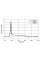
(DSC評価)
接着剤フィルムX1~X6について、パーキンエルマー社製の示差走査熱量計(商品名:DSC Q1000)を用いて、窒素(N2)雰囲気下、昇温速度10℃/分の条件で50℃から300℃までのDSC測定を実施し、発熱開始温度[℃]、ピークトップ温度[℃]、発熱終了温度[℃]、発熱量[J/g]を算出した。結果を表2及び図4~6に示す。
(DSC evaluation)
For the adhesive films X1 to X6, DSC measurements were carried out using a PerkinElmer differential scanning calorimeter (product name: DSC Q1000) under a nitrogen (N 2 ) atmosphere at a temperature rise rate of 10°C/min from 50°C to 300°C, and the heat generation start temperature [°C], peak top temperature [°C], heat generation end temperature [°C], and heat generation amount [J/g] were calculated. The results are shown in Table 2 and Figures 4 to 6.

実験例A1と実験例A2との対比、及び、実験例A3と実験例A4との対比により示されるように、カチオン重合性化合物として脂環式エポキシ化合物を用い、熱カチオン重合開始剤として、テトラキス[3,5-ビス(トリフルオロメチル)フェニル]ボレートアニオンを有するオニウム塩を用いることで、DSCの発熱開始温度及びピークトップ温度が低温化することが確認された。また、実験例A5と実験例A6との対比より、上記低温化が、カチオン重合性化合物として脂環式エポキシ化合物を用いた場合に特異的に生じる効果であることが確認された。 As shown by the comparison of Experimental Example A1 with Experimental Example A2, and the comparison of Experimental Example A3 with Experimental Example A4, it was confirmed that the heat generation onset temperature and peak top temperature of the DSC were lowered by using an alicyclic epoxy compound as the cationic polymerizable compound and an onium salt having a tetrakis[3,5-bis(trifluoromethyl)phenyl]borate anion as the thermal cationic polymerization initiator. In addition, the comparison of Experimental Example A5 with Experimental Example A6 confirmed that the above-mentioned lowering of the temperature is an effect that occurs specifically when an alicyclic epoxy compound is used as the cationic polymerizable compound.
(硬化物性の評価)
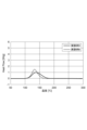
接着剤フィルムX3~X4について、硬化物性の評価を行った。具体的には、接着剤フィルムを複数枚用意し、200μmの厚さになるようにラミネートし、180℃のオーブンで1時間加熱することで、評価用の硬化フィルムを作製した。その後、硬化フィルムをTAインスツルメントジャパン株式会社製の動的粘弾性装置(商品名:RSA-3)を用いて、昇温速度10℃/分の条件で50℃から300℃までのDMA測定を行い、250℃での貯蔵弾性率を求めた。また、硬化フィルムをエスアイアイ・ナノテクノジー株式会社製のTG/DTA測定装置(商品名:TG/DTA7200)を用いて、昇温速度20℃/分の条件で100℃から400℃までのTG/DTA測定を行い、5%重量減少開始温度を求めた。結果を表3及び図7~8に示す。
(Evaluation of cured properties)
The cured physical properties of the adhesive films X3 to X4 were evaluated. Specifically, a plurality of adhesive films were prepared, laminated to a thickness of 200 μm, and heated in an oven at 180 ° C. for 1 hour to prepare a cured film for evaluation. Thereafter, the cured film was subjected to DMA measurement from 50 ° C. to 300 ° C. at a heating rate of 10 ° C./min using a dynamic viscoelasticity device (product name: RSA-3) manufactured by TA Instruments Japan Co., Ltd., to obtain the storage modulus at 250 ° C. In addition, the cured film was subjected to TG / DTA measurement from 100 ° C. to 400 ° C. at a heating rate of 20 ° C./min using a TG / DTA measurement device (product name: TG / DTA7200) manufactured by SII Nano Technology Co., Ltd., to obtain the 5% weight loss onset temperature. The results are shown in Table 3 and Figures 7 to 8.

実験例A3と実験例A4との対比により、カチオン重合性化合物として脂環式エポキシ化合物及びオキセタン化合物を用い、熱カチオン重合開始剤として、テトラキス[3,5-ビス(トリフルオロメチル)フェニル]ボレートアニオンを有するオニウム塩を用いることで、耐熱性が向上する(貯蔵弾性率が向上し、また、5%重量減少開始温度も高くなる)ことが確認された。 Comparing Experimental Example A3 and Experimental Example A4, it was confirmed that the heat resistance was improved (the storage modulus was improved and the 5% weight loss onset temperature was also increased) by using an alicyclic epoxy compound and an oxetane compound as the cationic polymerizable compound and an onium salt having a tetrakis[3,5-bis(trifluoromethyl)phenyl]borate anion as the thermal cationic polymerization initiator.
<実験例B1~B5>
(回路接続用接着剤の作製)
表4及び表5に示す各成分を同表に示す配合量(単位:質量部)で2-ブタノン(メチルエチルケトン)と混合することにより、第一の接着剤層を形成するためのワニス状の接着剤組成物(第一の接着剤組成物)Y1~Y4、及び、第二の接着剤層を形成するためのワニス状の接着剤組成物(第二の接着剤組成物)Z1~Z4を調製した。表中の各成分の配合量は不揮発分の配合量を表す。なお、熱カチオン重合開始剤の配合量は単位物質量当たりの質量が等しくなるように配合した。
<Experimental Examples B1 to B5>
(Preparation of Circuit Connection Adhesive)
Varnish-like adhesive compositions (first adhesive compositions) Y1 to Y4 for forming a first adhesive layer and varnish-like adhesive compositions (second adhesive compositions) Z1 to Z4 for forming a second adhesive layer were prepared by mixing each of the components shown in Tables 4 and 5 in the amounts (unit: parts by mass) shown in the tables with 2-butanone (methyl ethyl ketone). The amount of each component in the tables represents the amount of non-volatile matter. The amounts of the thermal cationic polymerization initiators were blended so that the mass per unit substance amount was equal.


表6に示す組み合わせで第一の接着剤組成物及び第二の接着剤組成物を用いて回路接続用接着剤フィルムを作製した。具体的には、まず、基材(PETフィルム)の上に第二の接着剤組成物を塗布し、乾燥させ、有機溶媒を除去することにより、基材上に厚さ11μmの第二の接着剤層を形成した。次いで、第二の接着剤層の上に第一の接着剤組成物を塗布し、乾燥させ、有機溶媒を除去することにより、第二の接着剤層上に厚さ7μmの第一の接着剤層を形成した。これにより、基材、第二の接着剤層及び第一の接着剤層がこの順に積層された異方導電フィルム(回路接続用接着剤フィルム)を作製した。 An adhesive film for circuit connection was produced using the first adhesive composition and the second adhesive composition in the combination shown in Table 6. Specifically, the second adhesive composition was first applied onto a substrate (PET film), dried, and the organic solvent was removed to form a second adhesive layer having a thickness of 11 μm on the substrate. Next, the first adhesive composition was applied onto the second adhesive layer, dried, and the organic solvent was removed to form a first adhesive layer having a thickness of 7 μm on the second adhesive layer. In this way, an anisotropic conductive film (adhesive film for circuit connection) was produced in which the substrate, the second adhesive layer, and the first adhesive layer were laminated in this order.
(接続構造体の作製)
第一の回路部材として、無アルカリガラス基板(OA-11、日本電気硝子株式会社製、外形:38mm×28mm、厚さ:0.3mm)の表面に、AlNd(100nm)/Mo(50nm)/ITO(100nm)の配線パターン(パターン幅:19μm、電極間スペース:5μm)を形成した配線付きガラス基板を準備した。第二の回路部材として、バンプ電極を2列で千鳥状に配列したICチップ(外形:0.9mm×20.3mm、厚さ:0.3mm、バンプ電極の大きさ:70μm×12μm、バンプ電極間スペース:12μm、バンプ電極厚さ:8μm)を準備した。
(Preparation of connection structure)
As a first circuit member, a glass substrate with wiring was prepared in which a wiring pattern (pattern width: 19 μm, space between electrodes: 5 μm) of AlNd (100 nm)/Mo (50 nm)/ITO (100 nm) was formed on the surface of an alkali-free glass substrate (OA-11, manufactured by Nippon Electric Glass Co., Ltd., outer dimensions: 38 mm×28 mm, thickness: 0.3 mm). As a second circuit member, an IC chip (outer dimensions: 0.9 mm×20.3 mm, thickness: 0.3 mm, bump electrode size: 70 μm×12 μm, space between bump electrodes: 12 μm, bump electrode thickness: 8 μm) in which bump electrodes were arranged in two rows in a staggered pattern was prepared.
上記で作製した異方導電フィルムを、第一の接着剤層と第一の回路部材の配線が形成されている面とが接するように、第一の回路部材上に配置した。セラミックヒータからなるステージとツール(8mm×50mm)とから構成される熱圧着装置(LD-06、株式会社大橋製作所製)を用いて、50℃、0.98MPa(10kgf/cm2)の条件で2秒間加熱及び加圧することにより、異方導電フィルムを第一の回路部材に貼り付けた。次いで、異方導電フィルムの第一の回路部材とは反対側の離型フィルムを剥離した。次いで、第一の回路部材の回路電極と第二の回路部材のバンプ電極との位置合わせを行った後、ヒートツールを8mm×45mmで用い、緩衝材として厚さ50μmのPTFEシートを介して、80℃に加熱した台座上で加熱・加圧した。実装温度(異方導電フィルムの実測最高到達温度)は115℃又は125℃とし、加熱時間は5秒間とし、加圧時の圧力(バンプ電極での面積換算圧力)は60MPaとした。これにより異方導電フィルムの第二の接着剤層を第二の回路部材に貼り付け、接続構造体を得た。 The anisotropic conductive film prepared above was placed on the first circuit member so that the first adhesive layer was in contact with the surface on which the wiring of the first circuit member was formed. Using a thermocompression bonding device (LD-06, manufactured by Ohashi Manufacturing Co., Ltd.) consisting of a stage made of a ceramic heater and a tool (8 mm x 50 mm), the anisotropic conductive film was attached to the first circuit member by heating and pressing for 2 seconds under conditions of 50°C and 0.98 MPa (10 kgf/cm 2 ). Next, the release film on the side of the anisotropic conductive film opposite to the first circuit member was peeled off. Next, after aligning the circuit electrodes of the first circuit member and the bump electrodes of the second circuit member, a heat tool of 8 mm x 45 mm was used to heat and press the anisotropic conductive film on a base heated to 80°C via a PTFE sheet having a thickness of 50 μm as a buffer material. The mounting temperature (the maximum temperature actually measured for the anisotropic conductive film) was 115° C. or 125° C., the heating time was 5 seconds, and the pressure applied (the pressure converted into the area of the bump electrode) was 60 MPa. In this way, the second adhesive layer of the anisotropic conductive film was attached to the second circuit member, and a connection structure was obtained.
<接続構造体の評価>
上記で作製した接続構造体について、初期(作製直後)及び高温高湿試験後の接続抵抗を四端子測定法で測定し、対向する電極間の電気的導通性を評価した。具体的には、マルチメータ(MLR21、楠本化成株式会社製)を用いて、14箇所で接続抵抗を測定し、接続抵抗値の最大値(最大抵抗値)を比較した。高温高湿試験は、温度85℃湿度85%RHの恒温恒湿槽にて接続構造体を250時間保管することにより行った。評価結果を表6に示す。
<Evaluation of connection structure>
The connection resistance of the connection structure produced above was measured by a four-terminal measurement method at the initial stage (immediately after production) and after the high temperature and humidity test to evaluate the electrical conductivity between the opposing electrodes. Specifically, the connection resistance was measured at 14 points using a multimeter (MLR21, manufactured by Kusumoto Chemical Co., Ltd.), and the maximum connection resistance values (maximum resistance values) were compared. The high temperature and humidity test was performed by storing the connection structure in a constant temperature and humidity chamber at a temperature of 85° C. and a humidity of 85% RH for 250 hours. The evaluation results are shown in Table 6.
また、接続構造体の初期(作製直後)及び高温高湿試験後、第一の回路部材の異方導電フィルムとの接着面の反対側から、FPD/LSI検査顕微鏡(株式会社ニコンインステック製、ECLIPSE L300ND)を用いて、第一の回路部材と回路接続部(異方導電フィルムの硬化物)との界面を観察し、剥離の有無を確認した。第一の回路部材と回路接続部との界面で剥離が発生しなかったものを評価A(接着性良好)、剥離が発生したものを評価B(接着不良)とした。評価結果を表6に示す。 In addition, the interface between the first circuit member and the circuit connection portion (cured product of the anisotropic conductive film) was observed using an FPD/LSI inspection microscope (Nikon Instech Corporation, ECLIPSE L300ND) from the opposite side of the adhesive surface of the first circuit member to the anisotropic conductive film at the initial stage (immediately after preparation) and after the high temperature and high humidity test to confirm the presence or absence of peeling. Those where no peeling occurred at the interface between the first circuit member and the circuit connection portion were rated A (good adhesion), and those where peeling occurred were rated B (poor adhesion). The evaluation results are shown in Table 6.
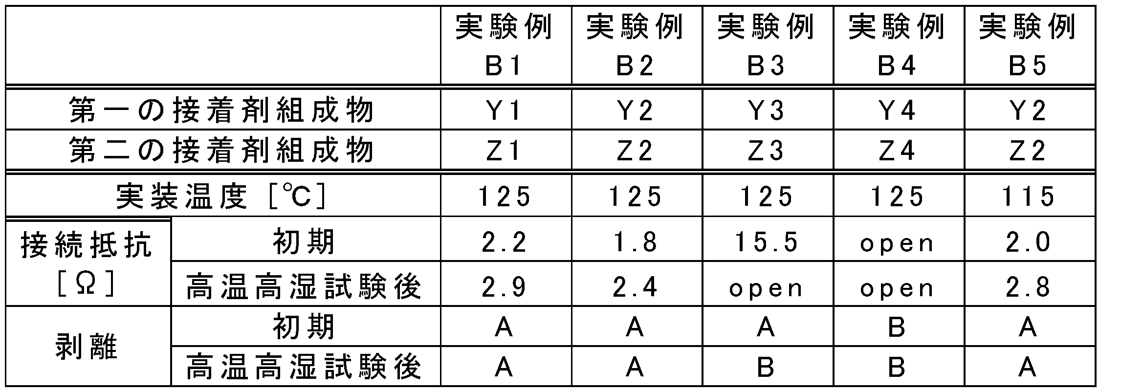
1…回路接続用接着剤フィルム、1A…第一の接着剤層、1B…第二の接着剤層、2A,2B…接着剤成分、3A…導電粒子、4…第一の回路部材、5…第二の回路部材、6…回路接続部、10…接続構造体、41…第一の回路基板、42…第一の電極、51…第二の回路基板、52…第二の電極。
1...adhesive film for circuit connection, 1A...first adhesive layer, 1B...second adhesive layer, 2A, 2B...adhesive component, 3A...conductive particles, 4...first circuit member, 5...second circuit member, 6...circuit connection portion, 10...connection structure, 41...first circuit board, 42...first electrode, 51...second circuit board, 52...second electrode.
Claims (6)
前記カチオン重合性化合物が、脂環式エポキシ化合物を含み、
前記熱カチオン重合開始剤が、下記式(1)で表されるアニオンを有するオニウム塩を含む、回路接続用接着剤。

the cationically polymerizable compound comprises an alicyclic epoxy compound,
The adhesive for circuit connection, wherein the thermal cationic polymerization initiator contains an onium salt having an anion represented by the following formula (1):
前記第一の接着剤層が、前記カチオン重合性化合物と、前記熱カチオン重合開始剤と、前記導電粒子と、を含有する、請求項3に記載の回路接続用接着剤。 A first adhesive layer and a second adhesive layer laminated on the first adhesive layer,
The adhesive for circuit connection according to claim 3 , wherein the first adhesive layer contains the cationically polymerizable compound, the thermal cationic polymerization initiator, and the conductive particles.
前記回路接続部が、請求項1~4のいずれか一項に記載の回路接続用接着剤の硬化物を含む、接続構造体。 a first circuit member having a first electrode, a second circuit member having a second electrode, and a circuit connection portion disposed between the first circuit member and the second circuit member, electrically connecting the first electrode and the second electrode to each other;
A connection structure, wherein the circuit connection portion comprises a cured product of the circuit connection adhesive according to any one of claims 1 to 4.
13. A method for manufacturing a connection structure, comprising the steps of: interposing the circuit connection adhesive according to any one of claims 1 to 4 between a first circuit member having a first electrode and a second circuit member having a second electrode; and thermocompression bonding the first circuit member and the second circuit member to electrically connect the first electrode and the second electrode to each other.
Priority Applications (1)
| Application Number | Priority Date | Filing Date | Title |
|---|---|---|---|
| JP2020198510A JP7608801B2 (en) | 2020-11-30 | 2020-11-30 | Adhesive for circuit connection, connection structure, and method for producing the connection structure |
Applications Claiming Priority (1)
| Application Number | Priority Date | Filing Date | Title |
|---|---|---|---|
| JP2020198510A JP7608801B2 (en) | 2020-11-30 | 2020-11-30 | Adhesive for circuit connection, connection structure, and method for producing the connection structure |
Publications (2)
| Publication Number | Publication Date |
|---|---|
| JP2022086478A JP2022086478A (en) | 2022-06-09 |
| JP7608801B2 true JP7608801B2 (en) | 2025-01-07 |
Family
ID=81894549
Family Applications (1)
| Application Number | Title | Priority Date | Filing Date |
|---|---|---|---|
| JP2020198510A Active JP7608801B2 (en) | 2020-11-30 | 2020-11-30 | Adhesive for circuit connection, connection structure, and method for producing the connection structure |
Country Status (1)
| Country | Link |
|---|---|
| JP (1) | JP7608801B2 (en) |
Families Citing this family (1)
| Publication number | Priority date | Publication date | Assignee | Title |
|---|---|---|---|---|
| JP2024099220A (en) * | 2023-01-12 | 2024-07-25 | 株式会社レゾナック | Adhesive composition, adhesive film for circuit connection, connection structure, and method for producing the connection structure |
Citations (10)
| Publication number | Priority date | Publication date | Assignee | Title |
|---|---|---|---|---|
| JP2000007684A (en) | 1998-06-16 | 2000-01-11 | Nippon Kayaku Co Ltd | Diaryliodonium salt type reaction initiator, energy-ray- curing composition containing the same and cured product of its composition |
| JP2011111557A (en) | 2009-11-27 | 2011-06-09 | Hitachi Chem Co Ltd | Adhesive composition, circuit connecting material, connector and connection method of circuit member, and semiconductor device |
| JP2011116977A (en) | 2009-11-05 | 2011-06-16 | Hitachi Chem Co Ltd | Thermopolymerization initiator system and adhesive composition |
| JP2012171980A (en) | 2011-02-17 | 2012-09-10 | Hitachi Chemical Co Ltd | Adhesive composition, circuit-connecting material, connected body, method for producing the same and semiconductor device |
| JP2017152354A (en) | 2016-02-22 | 2017-08-31 | デクセリアルズ株式会社 | Anisotropic conductive film |
| JP2017214472A (en) | 2016-05-31 | 2017-12-07 | 日立化成株式会社 | Adhesive composition and film-like adhesive composition |
| WO2018180685A1 (en) | 2017-03-30 | 2018-10-04 | デクセリアルズ株式会社 | Anisotropic electroconductive adhesive and production method for connection body |
| WO2018181536A1 (en) | 2017-03-29 | 2018-10-04 | 日立化成株式会社 | Adhesive composition and structural body |
| JP2018168345A (en) | 2017-03-30 | 2018-11-01 | デクセリアルズ株式会社 | Anisotropic conductive adhesive |
| WO2019050011A1 (en) | 2017-09-11 | 2019-03-14 | 日立化成株式会社 | Adhesive film for circuit connections and manufacturing method thereof, manufacturing method of circuit connection structure, and adhesive film housing set |
Family Cites Families (1)
| Publication number | Priority date | Publication date | Assignee | Title |
|---|---|---|---|---|
| JPH101507A (en) * | 1996-06-17 | 1998-01-06 | Toyo Ink Mfg Co Ltd | Polymerizable composition and cured product thereof |
-
2020
- 2020-11-30 JP JP2020198510A patent/JP7608801B2/en active Active
Patent Citations (10)
| Publication number | Priority date | Publication date | Assignee | Title |
|---|---|---|---|---|
| JP2000007684A (en) | 1998-06-16 | 2000-01-11 | Nippon Kayaku Co Ltd | Diaryliodonium salt type reaction initiator, energy-ray- curing composition containing the same and cured product of its composition |
| JP2011116977A (en) | 2009-11-05 | 2011-06-16 | Hitachi Chem Co Ltd | Thermopolymerization initiator system and adhesive composition |
| JP2011111557A (en) | 2009-11-27 | 2011-06-09 | Hitachi Chem Co Ltd | Adhesive composition, circuit connecting material, connector and connection method of circuit member, and semiconductor device |
| JP2012171980A (en) | 2011-02-17 | 2012-09-10 | Hitachi Chemical Co Ltd | Adhesive composition, circuit-connecting material, connected body, method for producing the same and semiconductor device |
| JP2017152354A (en) | 2016-02-22 | 2017-08-31 | デクセリアルズ株式会社 | Anisotropic conductive film |
| JP2017214472A (en) | 2016-05-31 | 2017-12-07 | 日立化成株式会社 | Adhesive composition and film-like adhesive composition |
| WO2018181536A1 (en) | 2017-03-29 | 2018-10-04 | 日立化成株式会社 | Adhesive composition and structural body |
| WO2018180685A1 (en) | 2017-03-30 | 2018-10-04 | デクセリアルズ株式会社 | Anisotropic electroconductive adhesive and production method for connection body |
| JP2018168345A (en) | 2017-03-30 | 2018-11-01 | デクセリアルズ株式会社 | Anisotropic conductive adhesive |
| WO2019050011A1 (en) | 2017-09-11 | 2019-03-14 | 日立化成株式会社 | Adhesive film for circuit connections and manufacturing method thereof, manufacturing method of circuit connection structure, and adhesive film housing set |
Also Published As
| Publication number | Publication date |
|---|---|
| JP2022086478A (en) | 2022-06-09 |
Similar Documents
| Publication | Publication Date | Title |
|---|---|---|
| JP7214912B2 (en) | Adhesive composition, adhesive film for circuit connection, connected structure, and method for producing connected structure | |
| JP2024099206A (en) | Adhesive composition, adhesive film for circuit connection, connection structure, and method for producing the connection structure | |
| WO2023136273A1 (en) | Adhesive composition, adhesive film for circuit connection, and method for producing connection structure | |
| JP7608801B2 (en) | Adhesive for circuit connection, connection structure, and method for producing the connection structure | |
| JP7608800B2 (en) | Adhesive for circuit connection, connection structure, and method for producing the connection structure | |
| WO2023068277A1 (en) | Adhesive tape for circuit connection, connection structure, and method for producing connection structure | |
| WO2022220285A1 (en) | Hardener, adhesive composition, adhesive film for circuit connection, connected structure, and method for producing connected structure | |
| JP7740254B2 (en) | Adhesive film for circuit connection, connection structure, and method for manufacturing the connection structure | |
| JP7729201B2 (en) | Adhesive composition, adhesive film for circuit connection, connection structure, and method for producing the connection structure | |
| JP2020107511A (en) | Anisotropic conductive film, cured product thereof and production method of anisotropic conductive film | |
| JP2024099224A (en) | Adhesive composition, adhesive film for circuit connection, connection structure, and method for producing connection structure | |
| JP2024099217A (en) | Adhesive composition, adhesive film for circuit connection, connection structure, and method for producing the connection structure | |
| JP2024099219A (en) | Adhesive composition, adhesive film for circuit connection, connection structure, and method for producing the connection structure | |
| JP2024099220A (en) | Adhesive composition, adhesive film for circuit connection, connection structure, and method for producing the connection structure | |
| JP2024099305A (en) | Adhesive composition, adhesive film for circuit connection, connection structure, and method for producing the connection structure | |
| JP6894221B2 (en) | Anisotropic conductive films, laminated films containing them, and methods for manufacturing them. | |
| WO2025018368A1 (en) | Adhesive composition, adhesive film for circuit connection, connected structure, and method for producing connected structure | |
| TW202229488A (en) | Adhesive film for circuit connection, and circuit connection structure and production method therefor |
Legal Events
| Date | Code | Title | Description |
|---|---|---|---|
| A621 | Written request for application examination |
Free format text: JAPANESE INTERMEDIATE CODE: A621 Effective date: 20231003 |
|
| A977 | Report on retrieval |
Free format text: JAPANESE INTERMEDIATE CODE: A971007 Effective date: 20240523 |
|
| A131 | Notification of reasons for refusal |
Free format text: JAPANESE INTERMEDIATE CODE: A131 Effective date: 20240528 |
|
| A601 | Written request for extension of time |
Free format text: JAPANESE INTERMEDIATE CODE: A601 Effective date: 20240729 |
|
| TRDD | Decision of grant or rejection written | ||
| A01 | Written decision to grant a patent or to grant a registration (utility model) |
Free format text: JAPANESE INTERMEDIATE CODE: A01 Effective date: 20241119 |
|
| A61 | First payment of annual fees (during grant procedure) |
Free format text: JAPANESE INTERMEDIATE CODE: A61 Effective date: 20241202 |
|
| R150 | Certificate of patent or registration of utility model |
Ref document number: 7608801 Country of ref document: JP Free format text: JAPANESE INTERMEDIATE CODE: R150 |