JP7602004B2 - 液晶光制御装置 - Google Patents
液晶光制御装置 Download PDFInfo
- Publication number
- JP7602004B2 JP7602004B2 JP2023500745A JP2023500745A JP7602004B2 JP 7602004 B2 JP7602004 B2 JP 7602004B2 JP 2023500745 A JP2023500745 A JP 2023500745A JP 2023500745 A JP2023500745 A JP 2023500745A JP 7602004 B2 JP7602004 B2 JP 7602004B2
- Authority
- JP
- Japan
- Prior art keywords
- liquid crystal
- crystal cell
- electrode
- substrate
- strip
- Prior art date
- Legal status (The legal status is an assumption and is not a legal conclusion. Google has not performed a legal analysis and makes no representation as to the accuracy of the status listed.)
- Active
Links
Images


Classifications
-
- G—PHYSICS
- G02—OPTICS
- G02F—OPTICAL DEVICES OR ARRANGEMENTS FOR THE CONTROL OF LIGHT BY MODIFICATION OF THE OPTICAL PROPERTIES OF THE MEDIA OF THE ELEMENTS INVOLVED THEREIN; NON-LINEAR OPTICS; FREQUENCY-CHANGING OF LIGHT; OPTICAL LOGIC ELEMENTS; OPTICAL ANALOGUE/DIGITAL CONVERTERS
- G02F1/00—Devices or arrangements for the control of the intensity, colour, phase, polarisation or direction of light arriving from an independent light source, e.g. switching, gating or modulating; Non-linear optics
- G02F1/01—Devices or arrangements for the control of the intensity, colour, phase, polarisation or direction of light arriving from an independent light source, e.g. switching, gating or modulating; Non-linear optics for the control of the intensity, phase, polarisation or colour
- G02F1/13—Devices or arrangements for the control of the intensity, colour, phase, polarisation or direction of light arriving from an independent light source, e.g. switching, gating or modulating; Non-linear optics for the control of the intensity, phase, polarisation or colour based on liquid crystals, e.g. single liquid crystal display cells
- G02F1/133—Constructional arrangements; Operation of liquid crystal cells; Circuit arrangements
- G02F1/1333—Constructional arrangements; Manufacturing methods
- G02F1/1343—Electrodes
-
- G—PHYSICS
- G02—OPTICS
- G02F—OPTICAL DEVICES OR ARRANGEMENTS FOR THE CONTROL OF LIGHT BY MODIFICATION OF THE OPTICAL PROPERTIES OF THE MEDIA OF THE ELEMENTS INVOLVED THEREIN; NON-LINEAR OPTICS; FREQUENCY-CHANGING OF LIGHT; OPTICAL LOGIC ELEMENTS; OPTICAL ANALOGUE/DIGITAL CONVERTERS
- G02F1/00—Devices or arrangements for the control of the intensity, colour, phase, polarisation or direction of light arriving from an independent light source, e.g. switching, gating or modulating; Non-linear optics
- G02F1/01—Devices or arrangements for the control of the intensity, colour, phase, polarisation or direction of light arriving from an independent light source, e.g. switching, gating or modulating; Non-linear optics for the control of the intensity, phase, polarisation or colour
- G02F1/13—Devices or arrangements for the control of the intensity, colour, phase, polarisation or direction of light arriving from an independent light source, e.g. switching, gating or modulating; Non-linear optics for the control of the intensity, phase, polarisation or colour based on liquid crystals, e.g. single liquid crystal display cells
- G02F1/133—Constructional arrangements; Operation of liquid crystal cells; Circuit arrangements
- G02F1/1333—Constructional arrangements; Manufacturing methods
- G02F1/1337—Surface-induced orientation of the liquid crystal molecules, e.g. by alignment layers
-
- G—PHYSICS
- G02—OPTICS
- G02F—OPTICAL DEVICES OR ARRANGEMENTS FOR THE CONTROL OF LIGHT BY MODIFICATION OF THE OPTICAL PROPERTIES OF THE MEDIA OF THE ELEMENTS INVOLVED THEREIN; NON-LINEAR OPTICS; FREQUENCY-CHANGING OF LIGHT; OPTICAL LOGIC ELEMENTS; OPTICAL ANALOGUE/DIGITAL CONVERTERS
- G02F1/00—Devices or arrangements for the control of the intensity, colour, phase, polarisation or direction of light arriving from an independent light source, e.g. switching, gating or modulating; Non-linear optics
- G02F1/01—Devices or arrangements for the control of the intensity, colour, phase, polarisation or direction of light arriving from an independent light source, e.g. switching, gating or modulating; Non-linear optics for the control of the intensity, phase, polarisation or colour
- G02F1/13—Devices or arrangements for the control of the intensity, colour, phase, polarisation or direction of light arriving from an independent light source, e.g. switching, gating or modulating; Non-linear optics for the control of the intensity, phase, polarisation or colour based on liquid crystals, e.g. single liquid crystal display cells
- G02F1/133—Constructional arrangements; Operation of liquid crystal cells; Circuit arrangements
- G02F1/1333—Constructional arrangements; Manufacturing methods
- G02F1/1343—Electrodes
- G02F1/134309—Electrodes characterised by their geometrical arrangement
- G02F1/134363—Electrodes characterised by their geometrical arrangement for applying an electric field parallel to the substrate, i.e. in-plane switching [IPS]
-
- G—PHYSICS
- G02—OPTICS
- G02F—OPTICAL DEVICES OR ARRANGEMENTS FOR THE CONTROL OF LIGHT BY MODIFICATION OF THE OPTICAL PROPERTIES OF THE MEDIA OF THE ELEMENTS INVOLVED THEREIN; NON-LINEAR OPTICS; FREQUENCY-CHANGING OF LIGHT; OPTICAL LOGIC ELEMENTS; OPTICAL ANALOGUE/DIGITAL CONVERTERS
- G02F1/00—Devices or arrangements for the control of the intensity, colour, phase, polarisation or direction of light arriving from an independent light source, e.g. switching, gating or modulating; Non-linear optics
- G02F1/01—Devices or arrangements for the control of the intensity, colour, phase, polarisation or direction of light arriving from an independent light source, e.g. switching, gating or modulating; Non-linear optics for the control of the intensity, phase, polarisation or colour
- G02F1/13—Devices or arrangements for the control of the intensity, colour, phase, polarisation or direction of light arriving from an independent light source, e.g. switching, gating or modulating; Non-linear optics for the control of the intensity, phase, polarisation or colour based on liquid crystals, e.g. single liquid crystal display cells
- G02F1/133—Constructional arrangements; Operation of liquid crystal cells; Circuit arrangements
- G02F1/1333—Constructional arrangements; Manufacturing methods
- G02F1/1347—Arrangement of liquid crystal layers or cells in which the final condition of one light beam is achieved by the addition of the effects of two or more layers or cells
- G02F1/13471—Arrangement of liquid crystal layers or cells in which the final condition of one light beam is achieved by the addition of the effects of two or more layers or cells in which all the liquid crystal cells or layers remain transparent, e.g. FLC, ECB, DAP, HAN, TN, STN, SBE-LC cells
-
- G—PHYSICS
- G02—OPTICS
- G02F—OPTICAL DEVICES OR ARRANGEMENTS FOR THE CONTROL OF LIGHT BY MODIFICATION OF THE OPTICAL PROPERTIES OF THE MEDIA OF THE ELEMENTS INVOLVED THEREIN; NON-LINEAR OPTICS; FREQUENCY-CHANGING OF LIGHT; OPTICAL LOGIC ELEMENTS; OPTICAL ANALOGUE/DIGITAL CONVERTERS
- G02F1/00—Devices or arrangements for the control of the intensity, colour, phase, polarisation or direction of light arriving from an independent light source, e.g. switching, gating or modulating; Non-linear optics
- G02F1/01—Devices or arrangements for the control of the intensity, colour, phase, polarisation or direction of light arriving from an independent light source, e.g. switching, gating or modulating; Non-linear optics for the control of the intensity, phase, polarisation or colour
- G02F1/13—Devices or arrangements for the control of the intensity, colour, phase, polarisation or direction of light arriving from an independent light source, e.g. switching, gating or modulating; Non-linear optics for the control of the intensity, phase, polarisation or colour based on liquid crystals, e.g. single liquid crystal display cells
- G02F1/133—Constructional arrangements; Operation of liquid crystal cells; Circuit arrangements
- G02F1/1333—Constructional arrangements; Manufacturing methods
- G02F1/1343—Electrodes
- G02F1/134309—Electrodes characterised by their geometrical arrangement
- G02F1/134336—Matrix
Landscapes
- Physics & Mathematics (AREA)
- Nonlinear Science (AREA)
- Mathematical Physics (AREA)
- Chemical & Material Sciences (AREA)
- Crystallography & Structural Chemistry (AREA)
- General Physics & Mathematics (AREA)
- Optics & Photonics (AREA)
- Geometry (AREA)
- Liquid Crystal (AREA)
- Spectroscopy & Molecular Physics (AREA)
- Optical Modulation, Optical Deflection, Nonlinear Optics, Optical Demodulation, Optical Logic Elements (AREA)
Description
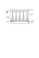
液晶光制御装置100は、液晶光制御素子102の各液晶セルに印加する制御信号の選択により、光源部(106)から放射される光の配光パターンを様々に制御することができる。図9は、一例として、光源部(106)から放射される光を四角形状の配光パターンに制御する場合を示す。

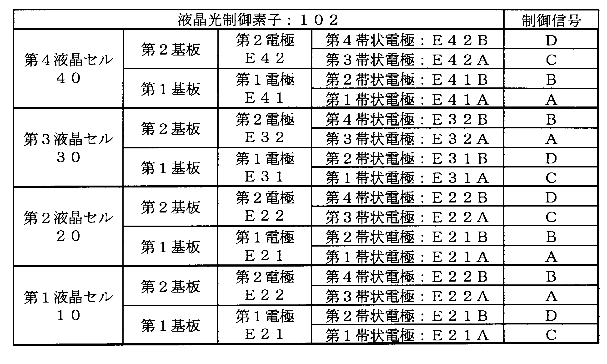
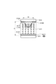
図12は、光源部106から放射される光を十字状の配光パターンに制御する一例を示す。図12に示す液晶光制御素子102の各液晶セルの配置は、図9と同じである。


図13は、光源部106から放射される光をライン状(X軸方向)の配光パターンに制御する一例を示す。図13に示す液晶光制御素子102の各液晶セルの配置は、図9と同じである。


図14は、光源部106から放射される光をライン状(Y軸方向)の配光パターンに制御する一例を示す。図14に示す液晶光制御素子102の各液晶セルの配置は、図9と同じである。


Claims (8)
- 第1液晶セルと、
第2液晶セルと、
第3液晶セルと、
第4液晶セルと、を含み、
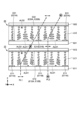
前記第1乃至第4液晶セルは、光が入射する側から、前記第1液晶セル、前記第2液晶セル、前記第3液晶セル、及び前記第4液晶セルがこの順番で重なるように配置され、
前記第1液晶セル、前記第2液晶セル、前記第3液晶セル、及び前記第4液晶セルのそれぞれは、
帯状パターンを含む第1電極が設けられた第1基板と、
帯状パターン含む第2電極が設けられた第2基板と、
前記第1基板に設けられた第1配向膜と、
前記第2基板に設けられた第2配向膜と、
前記第1基板と前記第2基板との間の液晶層と、を含み、
前記第1電極は、前記帯状パターンを有する少なくとも1つの第1帯状電極と、前記帯状パターンを有する少なくとも1つの第2帯状電極と、を含み、前記少なくとも1つの第1帯状電極と前記少なくとも1つの第2帯状電極とは離隔して交互に配置され、
前記第2電極は、前記帯状パターンを有する少なくとも1つの第3帯状電極と、前記帯状パターンを有する少なくとも1つの第4帯状電極と、を含み、前記少なくとも1つの第3帯状電極と前記少なくとも1つの第4帯状電極とは離隔して交互に配置され、
前記第1電極及び前記第2電極の前記帯状パターンの長手方向が交差するように前記第1基板と前記第2基板とが配置され、
前記第1配向膜の配向方向が前記第1電極の前記帯状パターンの長手方向と交差する方向であり、
前記第2配向膜の配向方向が前記第2電極の前記帯状パターンの長手方向と交差する方向であり、
前記第1液晶セル、前記第2液晶セル、前記第3液晶セル、及び前記第4液晶セルの内、2つの液晶セルは前記第1電極の帯状パターンの長手方向が第1方向と平行な方向に配置され、他の2つの液晶セルの第1電極の帯状パターンの長手方向は、前記第1方向と交差する第2方向と平行な方向に配置されている、ことを特徴とする液晶光制御装置。 - 前記第1液晶セルの第1電極と前記第2液晶セルの第1電極とは前記帯状パターンの長手方向が前記第1方向と平行な方向に配置され、前記第1液晶セルの第2電極と前記第2液晶セルの第2電極とは前記帯状パターンの長手方向が前記第2方向と平行な方向に配置され、
前記第3液晶セルの第1電極と前記第4液晶セルの第1電極とは前記帯状パターンの長手方向が前記第2方向と平行な方向に配置され、前記第3液晶セルの第2電極と前記第4液晶セルの第2電極とは前記帯状パターンの長手方向が前記第1方向と平行な方向に配置されている、請求項1に記載の液晶光制御装置。 - 前記第1液晶セルの第1電極と前記第3液晶セルの第1電極とは前記帯状パターンの長手方向が前記第1方向と平行な方向に配置され、前記第1液晶セルの第2電極と前記第3液晶セルの第2電極とは前記帯状パターンの長手方向が前記第2方向と平行な方向に配置され、
前記第2液晶セルの第1電極と前記第4液晶セルの第1電極とは前記帯状パターンの長手方向が前記第2方向と平行な方向に配置され、前記第2液晶セルの第2電極と前記第4液晶セルの第2電極とは前記帯状パターンの長手方向が前記第1方向と平行な方向に配置されている、請求項1に記載の液晶光制御装置。 - 前記第1液晶セルの第2基板と前記第2液晶セルの第2基板とが隣接し、
前記第2液晶セルの第1基板と前記第3液晶セルの第1基板とが隣接し、
前記第3液晶セルの第2基板と前記第4液晶セルの第2基板とが隣接している、請求項3に記載の液晶光制御装置。 - 前記第1電極は、前記第1帯状電極と前記第2帯状電極との間で横電界を発生させ、前記第2電極は、前記第3帯状電極と前記第4帯状電極との間で横電界を発生させる、請求項1に記載の液晶光制御装置。
- 前記第1液晶セル、前記第2液晶セル、前記第3液晶セル、前記第4液晶セルの前記液晶層の厚さが、前記第1帯状電極と前記第2帯状電極の中心間距離の1倍以上の長さを有する、請求項1に記載の液晶光制御装置。
- 前記第1液晶セル、前記第2液晶セル、前記第3液晶セル、及び前記第4液晶セルのそれぞれは、前記液晶層が、前記第1電極で発生する横電界と前記第2電極で発生する横電界とが干渉しない厚さを有する、請求項1に記載の液晶光制御装置。
- 前記液晶層が、ねじれネマチック液晶である、請求項1に記載の液晶光制御装置。
Priority Applications (2)
| Application Number | Priority Date | Filing Date | Title |
|---|---|---|---|
| JP2024212267A JP7716561B2 (ja) | 2021-02-18 | 2024-12-05 | 液晶光制御装置 |
| JP2025121233A JP2025143527A (ja) | 2021-02-18 | 2025-07-18 | 液晶光制御装置 |
Applications Claiming Priority (3)
| Application Number | Priority Date | Filing Date | Title |
|---|---|---|---|
| JP2021024713 | 2021-02-18 | ||
| JP2021024713 | 2021-02-18 | ||
| PCT/JP2022/004747 WO2022176684A1 (ja) | 2021-02-18 | 2022-02-07 | 液晶光制御装置 |
Related Child Applications (1)
| Application Number | Title | Priority Date | Filing Date |
|---|---|---|---|
| JP2024212267A Division JP7716561B2 (ja) | 2021-02-18 | 2024-12-05 | 液晶光制御装置 |
Publications (2)
| Publication Number | Publication Date |
|---|---|
| JPWO2022176684A1 JPWO2022176684A1 (ja) | 2022-08-25 |
| JP7602004B2 true JP7602004B2 (ja) | 2024-12-17 |
Family
ID=82930500
Family Applications (3)
| Application Number | Title | Priority Date | Filing Date |
|---|---|---|---|
| JP2023500745A Active JP7602004B2 (ja) | 2021-02-18 | 2022-02-07 | 液晶光制御装置 |
| JP2024212267A Active JP7716561B2 (ja) | 2021-02-18 | 2024-12-05 | 液晶光制御装置 |
| JP2025121233A Pending JP2025143527A (ja) | 2021-02-18 | 2025-07-18 | 液晶光制御装置 |
Family Applications After (2)
| Application Number | Title | Priority Date | Filing Date |
|---|---|---|---|
| JP2024212267A Active JP7716561B2 (ja) | 2021-02-18 | 2024-12-05 | 液晶光制御装置 |
| JP2025121233A Pending JP2025143527A (ja) | 2021-02-18 | 2025-07-18 | 液晶光制御装置 |
Country Status (9)
| Country | Link |
|---|---|
| US (2) | US12216363B2 (ja) |
| EP (1) | EP4296769B1 (ja) |
| JP (3) | JP7602004B2 (ja) |
| KR (1) | KR102811455B1 (ja) |
| CN (1) | CN116830030B (ja) |
| BR (1) | BR112023016456A2 (ja) |
| CA (1) | CA3207954A1 (ja) |
| MX (1) | MX2023009609A (ja) |
| WO (1) | WO2022176684A1 (ja) |
Families Citing this family (9)
| Publication number | Priority date | Publication date | Assignee | Title |
|---|---|---|---|---|
| JP7817910B2 (ja) * | 2022-09-28 | 2026-02-19 | 株式会社ジャパンディスプレイ | 電気光学装置および照明装置 |
| CN119816780A (zh) * | 2022-10-19 | 2025-04-11 | 株式会社日本显示器 | 光学元件以及照明装置 |
| JP7796893B2 (ja) * | 2022-10-25 | 2026-01-09 | 株式会社ジャパンディスプレイ | 照明装置 |
| WO2024090049A1 (ja) * | 2022-10-25 | 2024-05-02 | 株式会社ジャパンディスプレイ | 照明装置とその駆動方法 |
| CN120225949A (zh) * | 2022-11-02 | 2025-06-27 | 株式会社日本显示器 | 照明装置 |
| CN120435702A (zh) * | 2022-12-21 | 2025-08-05 | 株式会社日本显示器 | 照明装置的控制装置 |
| CN120500661A (zh) * | 2023-02-21 | 2025-08-15 | 株式会社日本显示器 | 照明装置 |
| CN121444004A (zh) * | 2023-07-21 | 2026-01-30 | 株式会社日本显示器 | 液晶光控制装置 |
| CN121729640A (zh) * | 2023-09-21 | 2026-03-24 | 株式会社日本显示器 | 液晶光学元件及照明装置 |
Citations (2)
| Publication number | Priority date | Publication date | Assignee | Title |
|---|---|---|---|---|
| JP2016506541A (ja) | 2012-12-18 | 2016-03-03 | レンズヴェクター インコーポレイテッドLensvector Incorporated | 高度な電界制御能力を備えた液晶光学装置 |
| US20190025657A1 (en) | 2015-09-12 | 2019-01-24 | Lensvector Inc. | Liquid crystal beam control device |
Family Cites Families (11)
| Publication number | Priority date | Publication date | Assignee | Title |
|---|---|---|---|---|
| JPH0764081A (ja) * | 1993-08-31 | 1995-03-10 | Toshiba Lighting & Technol Corp | 照明装置,バックライト,液晶表示装置および表示装置 |
| JP4471729B2 (ja) | 2004-04-30 | 2010-06-02 | シチズン電子株式会社 | 液晶レンズ付き発光装置 |
| EP2140304B1 (en) | 2007-04-17 | 2011-08-31 | Koninklijke Philips Electronics N.V. | Beam-shaping device |
| JP5417005B2 (ja) | 2009-03-26 | 2014-02-12 | パナソニック株式会社 | 照明装置 |
| CN102231033B (zh) * | 2011-05-27 | 2014-11-05 | 深圳超多维光电子有限公司 | 液晶透镜及其控制方法、3d显示装置以及计算机系统 |
| US10126607B2 (en) * | 2015-09-12 | 2018-11-13 | Lensvector Inc. | Liquid crystal beam control device |
| CN105702171A (zh) * | 2016-04-19 | 2016-06-22 | 京东方科技集团股份有限公司 | 显示装置及显示方法 |
| JP6783461B2 (ja) * | 2016-10-18 | 2020-11-11 | 国立大学法人 筑波大学 | 光計測システムおよび光計測方法 |
| CN108267897A (zh) * | 2016-12-30 | 2018-07-10 | 深圳超多维光电子有限公司 | 偏振成像装置和方法 |
| KR20180108977A (ko) * | 2017-03-24 | 2018-10-05 | 에스케이씨하이테크앤마케팅(주) | 무안경 입체 영상 표시 장치용 필름 |
| CN110582719B (zh) * | 2017-04-20 | 2021-11-30 | 兰斯维克托公司 | 具有改进光束匀称性的液晶光束拓宽装置 |
-
2022
- 2022-02-07 CN CN202280014059.9A patent/CN116830030B/zh active Active
- 2022-02-07 EP EP22756005.9A patent/EP4296769B1/en active Active
- 2022-02-07 WO PCT/JP2022/004747 patent/WO2022176684A1/ja not_active Ceased
- 2022-02-07 MX MX2023009609A patent/MX2023009609A/es unknown
- 2022-02-07 CA CA3207954A patent/CA3207954A1/en active Pending
- 2022-02-07 BR BR112023016456A patent/BR112023016456A2/pt unknown
- 2022-02-07 JP JP2023500745A patent/JP7602004B2/ja active Active
- 2022-02-07 KR KR1020237026551A patent/KR102811455B1/ko active Active
-
2023
- 2023-08-08 US US18/231,306 patent/US12216363B2/en active Active
-
2024
- 2024-12-05 JP JP2024212267A patent/JP7716561B2/ja active Active
- 2024-12-19 US US18/988,096 patent/US20250116900A1/en active Pending
-
2025
- 2025-07-18 JP JP2025121233A patent/JP2025143527A/ja active Pending
Patent Citations (2)
| Publication number | Priority date | Publication date | Assignee | Title |
|---|---|---|---|---|
| JP2016506541A (ja) | 2012-12-18 | 2016-03-03 | レンズヴェクター インコーポレイテッドLensvector Incorporated | 高度な電界制御能力を備えた液晶光学装置 |
| US20190025657A1 (en) | 2015-09-12 | 2019-01-24 | Lensvector Inc. | Liquid crystal beam control device |
Also Published As
| Publication number | Publication date |
|---|---|
| CN116830030A (zh) | 2023-09-29 |
| JP2025023292A (ja) | 2025-02-14 |
| US20250116900A1 (en) | 2025-04-10 |
| EP4296769A1 (en) | 2023-12-27 |
| BR112023016456A2 (pt) | 2023-10-10 |
| WO2022176684A1 (ja) | 2022-08-25 |
| CA3207954A1 (en) | 2022-08-25 |
| KR102811455B1 (ko) | 2025-05-22 |
| US20230375883A1 (en) | 2023-11-23 |
| JPWO2022176684A1 (ja) | 2022-08-25 |
| JP7716561B2 (ja) | 2025-07-31 |
| EP4296769A4 (en) | 2025-01-08 |
| US12216363B2 (en) | 2025-02-04 |
| EP4296769B1 (en) | 2026-04-08 |
| MX2023009609A (es) | 2023-10-25 |
| CN116830030B (zh) | 2026-02-13 |
| KR20230125321A (ko) | 2023-08-29 |
| JP2025143527A (ja) | 2025-10-01 |
Similar Documents
| Publication | Publication Date | Title |
|---|---|---|
| JP7602004B2 (ja) | 液晶光制御装置 | |
| JP7703758B2 (ja) | 液晶光制御装置 | |
| JP7527472B2 (ja) | 液晶光制御装置 | |
| JP7776500B2 (ja) | 光学装置 | |
| WO2021157225A1 (ja) | 光制御装置及び照明装置 | |
| JP7592879B2 (ja) | 液晶光制御素子及び照明装置 | |
| JP7565454B2 (ja) | 光学素子の駆動方法 | |
| HK40092860A (zh) | 液晶光控制装置 | |
| HK40096212A (zh) | 液晶光控制装置 | |
| CN121444004A (zh) | 液晶光控制装置 | |
| HK40102873A (zh) | 液晶光控制元件以及照明装置 |
Legal Events
| Date | Code | Title | Description |
|---|---|---|---|
| A621 | Written request for application examination |
Free format text: JAPANESE INTERMEDIATE CODE: A621 Effective date: 20230807 |
|
| A131 | Notification of reasons for refusal |
Free format text: JAPANESE INTERMEDIATE CODE: A131 Effective date: 20240402 |
|
| A601 | Written request for extension of time |
Free format text: JAPANESE INTERMEDIATE CODE: A601 Effective date: 20240522 |
|
| A521 | Request for written amendment filed |
Free format text: JAPANESE INTERMEDIATE CODE: A523 Effective date: 20240704 |
|
| A131 | Notification of reasons for refusal |
Free format text: JAPANESE INTERMEDIATE CODE: A131 Effective date: 20240903 |
|
| A521 | Request for written amendment filed |
Free format text: JAPANESE INTERMEDIATE CODE: A523 Effective date: 20241017 |
|
| TRDD | Decision of grant or rejection written | ||
| A01 | Written decision to grant a patent or to grant a registration (utility model) |
Free format text: JAPANESE INTERMEDIATE CODE: A01 Effective date: 20241105 |
|
| A61 | First payment of annual fees (during grant procedure) |
Free format text: JAPANESE INTERMEDIATE CODE: A61 Effective date: 20241205 |
|
| R150 | Certificate of patent or registration of utility model |
Ref document number: 7602004 Country of ref document: JP Free format text: JAPANESE INTERMEDIATE CODE: R150 |