JP7586866B2 - Focused Ion Beam Equipment - Google Patents
Focused Ion Beam Equipment Download PDFInfo
- Publication number
- JP7586866B2 JP7586866B2 JP2022136135A JP2022136135A JP7586866B2 JP 7586866 B2 JP7586866 B2 JP 7586866B2 JP 2022136135 A JP2022136135 A JP 2022136135A JP 2022136135 A JP2022136135 A JP 2022136135A JP 7586866 B2 JP7586866 B2 JP 7586866B2
- Authority
- JP
- Japan
- Prior art keywords
- processing
- ion beam
- setting
- irradiation current
- area
- Prior art date
- Legal status (The legal status is an assumption and is not a legal conclusion. Google has not performed a legal analysis and makes no representation as to the accuracy of the status listed.)
- Active
Links
Images


Classifications
-
- H—ELECTRICITY
- H01—ELECTRIC ELEMENTS
- H01J—ELECTRIC DISCHARGE TUBES OR DISCHARGE LAMPS
- H01J37/00—Discharge tubes with provision for introducing objects or material to be exposed to the discharge, e.g. for the purpose of examination or processing thereof
- H01J37/30—Electron-beam or ion-beam tubes for localised treatment of objects
- H01J37/3002—Details
- H01J37/3007—Electron or ion-optical systems
-
- H—ELECTRICITY
- H01—ELECTRIC ELEMENTS
- H01J—ELECTRIC DISCHARGE TUBES OR DISCHARGE LAMPS
- H01J37/00—Discharge tubes with provision for introducing objects or material to be exposed to the discharge, e.g. for the purpose of examination or processing thereof
- H01J37/02—Details
- H01J37/20—Means for supporting or positioning the object or the material; Means for adjusting diaphragms or lenses associated with the support
-
- H—ELECTRICITY
- H01—ELECTRIC ELEMENTS
- H01J—ELECTRIC DISCHARGE TUBES OR DISCHARGE LAMPS
- H01J37/00—Discharge tubes with provision for introducing objects or material to be exposed to the discharge, e.g. for the purpose of examination or processing thereof
- H01J37/30—Electron-beam or ion-beam tubes for localised treatment of objects
- H01J37/302—Controlling tubes by external information, e.g. programme control
-
- H—ELECTRICITY
- H01—ELECTRIC ELEMENTS
- H01J—ELECTRIC DISCHARGE TUBES OR DISCHARGE LAMPS
- H01J37/00—Discharge tubes with provision for introducing objects or material to be exposed to the discharge, e.g. for the purpose of examination or processing thereof
- H01J37/30—Electron-beam or ion-beam tubes for localised treatment of objects
- H01J37/305—Electron-beam or ion-beam tubes for localised treatment of objects for casting, melting, evaporating, or etching
- H01J37/3053—Electron-beam or ion-beam tubes for localised treatment of objects for casting, melting, evaporating, or etching for evaporating or etching
- H01J37/3056—Electron-beam or ion-beam tubes for localised treatment of objects for casting, melting, evaporating, or etching for evaporating or etching for microworking, e. g. etching of gratings or trimming of electrical components
-
- H—ELECTRICITY
- H01—ELECTRIC ELEMENTS
- H01J—ELECTRIC DISCHARGE TUBES OR DISCHARGE LAMPS
- H01J2237/00—Discharge tubes exposing object to beam, e.g. for analysis treatment, etching, imaging
- H01J2237/30—Electron or ion beam tubes for processing objects
- H01J2237/304—Controlling tubes
- H01J2237/30472—Controlling the beam
- H01J2237/30483—Scanning
-
- H—ELECTRICITY
- H01—ELECTRIC ELEMENTS
- H01J—ELECTRIC DISCHARGE TUBES OR DISCHARGE LAMPS
- H01J2237/00—Discharge tubes exposing object to beam, e.g. for analysis treatment, etching, imaging
- H01J2237/30—Electron or ion beam tubes for processing objects
- H01J2237/317—Processing objects on a microscale
- H01J2237/3174—Etching microareas
- H01J2237/31745—Etching microareas for preparing specimen to be viewed in microscopes or analyzed in microanalysers
-
- H—ELECTRICITY
- H01—ELECTRIC ELEMENTS
- H01J—ELECTRIC DISCHARGE TUBES OR DISCHARGE LAMPS
- H01J2237/00—Discharge tubes exposing object to beam, e.g. for analysis treatment, etching, imaging
- H01J2237/30—Electron or ion beam tubes for processing objects
- H01J2237/317—Processing objects on a microscale
- H01J2237/31749—Focused ion beam
Landscapes
- Chemical & Material Sciences (AREA)
- Analytical Chemistry (AREA)
- Physics & Mathematics (AREA)
- Engineering & Computer Science (AREA)
- Plasma & Fusion (AREA)
- Sampling And Sample Adjustment (AREA)
- Welding Or Cutting Using Electron Beams (AREA)
- Drying Of Semiconductors (AREA)
Description
本発明は、集束イオンビーム装置に関する。 The present invention relates to a focused ion beam device.
集束イオンビーム装置は、集束させたイオンビームで試料表面を走査することによって、試料を加工する装置である。 A focused ion beam device is a device that processes samples by scanning the sample surface with a focused ion beam.
集束イオンビーム装置において、試料の断面を作製する場合、最初にイオンビームの照射電流を大きくして粗加工し、その後、イオンビームの照射電流を小さくして仕上げ加工する。これにより、短時間で、きれいな断面を得ることができる。このように、集束イオンビーム装置では、照射電流などの加工条件を変更しながら、加工を進める。 When preparing a cross-section of a sample using a focused ion beam device, the ion beam's projection current is first increased to perform rough processing, and then the ion beam's projection current is decreased to perform finish processing. This allows a clean cross-section to be obtained in a short amount of time. In this way, with a focused ion beam device, processing proceeds while changing processing conditions such as the projection current.
例えば、特許文献1には、ユーザーが加工領域の大きさや加工仕上げ具合などのデータを入力すると、ビーム径などの加工条件を自動で算出する集束イオンビーム装置が開示されている。
For example,
特許文献1に開示された集束イオンビーム装置では、ユーザーが設定した1つの加工領域に対して1つの加工条件しか設定できない。そのため、照射電流などの加工条件を変更しながら加工を進める場合には、ユーザーは加工領域を何度も設定しなければならない。
In the focused ion beam device disclosed in
本発明に係る集束イオンビーム装置の一態様は、
試料をイオンビームで走査することによって、前記試料の断面を加工する集束イオンビーム装置であって、
前記試料を前記イオンビームで走査する光学系と、
前記試料の加工領域の設定、および1つの前記加工領域に対する複数の加工条件の設定を受け付ける受付部と、
前記光学系を制御する制御部と、
を含み、
前記制御部は、1つの前記加工領域内に対して設定された複数の加工条件に基づいて、前記光学系に前記加工領域を前記イオンビームで走査させ、
前記受付部は、前記加工領域を前記イオンビームで走査するときの走査線ごとに加工条件の設定を受け付け、
前記制御部は、走査線ごとに設定された加工条件に基づいて、前記光学系に前記加工領域を前記イオンビームで走査させる。
本発明に係る集束イオンビーム装置の一態様は、
試料をイオンビームで走査することによって、前記試料の断面を加工する集束イオンビーム装置であって、
前記試料を前記イオンビームで走査する光学系と、
前記試料の加工領域の設定、および1つの前記加工領域に対する複数の加工条件の設定を受け付ける受付部と、
前記光学系を制御する制御部と、
前記加工条件を設定する設定部と、
を含み、
前記制御部は、1つの前記加工領域内に対して設定された複数の加工条件に基づいて、前記光学系に前記加工領域を前記イオンビームで走査させ、
前記加工条件は、前記イオンビームの照射電流を含み、
前記設定部は、設定された前記加工領域に基づいて、前記イオンビームの最大照射電流である第1照射電流を設定する。
One aspect of the focused ion beam device according to the present invention is
1. A focused ion beam apparatus for processing a cross section of a sample by scanning the sample with an ion beam, comprising:
an optical system for scanning the sample with the ion beam;
A reception unit that receives a setting of a processing area of the sample and a setting of a plurality of processing conditions for one of the processing areas;
A control unit that controls the optical system;
Including,
The control unit causes the optical system to scan the processing region with the ion beam based on a plurality of processing conditions set for one of the processing regions ;
the reception unit receives settings of processing conditions for each scanning line when scanning the processing region with the ion beam;
The control unit causes the optical system to scan the processing region with the ion beam based on processing conditions set for each scanning line .
One aspect of the focused ion beam device according to the present invention is
1. A focused ion beam apparatus for processing a cross section of a sample by scanning the sample with an ion beam, comprising:
an optical system for scanning the sample with the ion beam;
A reception unit that receives a setting of a processing area of the sample and a setting of a plurality of processing conditions for one of the processing areas;
A control unit that controls the optical system;
A setting unit for setting the processing conditions;
Including,
The control unit causes the optical system to scan the processing region with the ion beam based on a plurality of processing conditions set for one of the processing regions;
the processing conditions include a irradiation current of the ion beam,
The setting unit sets a first irradiation current that is a maximum irradiation current of the ion beam based on the set processing area .
このような集束イオンビーム装置では、1つの加工領域に複数の加工条件を設定できる。そのため、このような集束イオンビーム装置では、ユーザーは加工条件を変更するごとに加工領域を設定しなくてもよく、容易に複数の加工条件を設定できる。 In such a focused ion beam device, multiple processing conditions can be set for one processing area. Therefore, in such a focused ion beam device, the user does not have to set the processing area every time the processing conditions are changed, and multiple processing conditions can be easily set.
以下、本発明の好適な実施形態について図面を用いて詳細に説明する。なお、以下に説明する実施形態は、特許請求の範囲に記載された本発明の内容を不当に限定するものではない。また、以下で説明される構成の全てが本発明の必須構成要件であるとは限らない。 Below, preferred embodiments of the present invention are described in detail with reference to the drawings. Note that the embodiments described below do not unduly limit the content of the present invention described in the claims. Furthermore, not all of the configurations described below are necessarily essential components of the present invention.
1. 第1実施形態
1.1. 集束イオンビーム装置
まず、第1実施形態に係る集束イオンビーム装置について図面を参照しながら説明する。図1は、第1実施形態に係る集束イオンビーム装置100の構成を示す図である。
1. First embodiment 1.1 Focused ion beam device First, a focused ion beam device according to a first embodiment will be described with reference to the drawings. Fig. 1 is a diagram showing the configuration of a focused
集束イオンビーム装置100は、図1に示すように、光学系10と、試料ステージ20と、二次電子検出器30と、ガス銃40と、処理部50と、操作部60と、表示部62と、記憶部64と、を含む。
As shown in FIG. 1, the focused
集束イオンビーム装置100では、集束したイオンビームIBで試料Sを走査することによって、試料Sを加工(エッチング)できる。また、集束イオンビーム装置100では、試料S表面付近にガス銃40によってガスを供給しながら、イオンビームIBを照射することで、試料S上にデポジション膜を形成できる。また、集束イオンビーム装置100では、集束したイオンビームIBで試料Sを走査し、試料Sから放出された電子を二次電子検出器30で検出することによって、SIM像(scanning ion microscope image)を取得できる。
In the focused
光学系10は、イオンビームIBで試料Sを走査する。光学系10は、イオン源11と、引出電極12と、加速電極13と、集束レンズ14と、ビームブランキング電極15と、可変マルチアパーチャー16と、ビーム偏向電極17と、対物レンズ18と、を含む。
The
イオン源11は、イオンを発生させる。引出電極12は、イオン源11からイオンを引き出す。加速電極13は、イオン源11から引き出されたイオンを加速させる。これにより、所定の加速電圧でイオンを加速させることができる。集束レンズ14は、イオンビームIBを集束させる。
The
ビームブランキング電極15は、イオンビームIBの試料Sへの照射のオン・オフを制御する。可変マルチアパーチャー16は、イオンビームIBの照射電流を選択的に制限する。可変マルチアパーチャー16は径の異なる複数の絞り孔を有している。集束イオンビーム装置100では、イオンビームIBの経路上に配置される絞り孔を切り替えることによって、イオンビームIBの照射電流を制御できる。
The
ビーム偏向電極17は、イオンビームIBを偏向する。ビーム偏向電極17によってイオンビームIBを偏向させることで、イオンビームIBで試料S上を二次元的に走査できる。対物レンズ18は、イオンビームIBを集束させる。
The
試料ステージ20は、試料Sを支持する。試料ステージ20は、試料Sを水平方向に移動させることができる。試料ステージ20は、さらに、試料Sを回転させたり、傾斜させたりすることができる。
The
二次電子検出器30は、イオンビームIBが試料Sに照射されることにより、試料Sで発生した二次電子を検出する。二次電子検出器30で検出された二次電子の検出信号(強度信号)は、イオンビームIBの走査と同期した画像データとして、処理部50に送られる。処理部50は、画像データに基づいてSIM像を生成し、表示部62に表示させる。
The
ガス銃40は、化合物ガスを試料Sの表面に供給する。化合物ガスを試料Sの表面に充満させたところにイオンビームIBを照射すると、イオンビームIBが試料Sに照射されることによって発生する二次電子によって、化合物ガスが分解される。分解された化合物ガスは、試料表面に吸着し堆積する。これにより、デポジション膜が成膜される。例えば、化合物ガスとして、W(CO)6を用いた場合、タングステン膜が成膜される。
The
操作部60は、ユーザーによる操作に応じた操作信号を取得し、処理部50に送る。操作部60は、例えば、ボタン、キー、タッチパネル型ディスプレイ、マイクなどの入力機器である。ユーザーは、操作部60を介して、加工領域および加工条件を設定できる。
The
表示部62は、処理部50で生成された画像を表示させる。表示部62は、例えば、LCD(liquid crystal display)などのディスプレイにより実現できる。表示部62には、例えば、GUI(Graphical User Interface)画面やSIM像が表示される。
The
記憶部64は、処理部50が各種計算処理や制御処理を行うためのプログラムやデータを記憶している。また、記憶部64は、処理部50のワーク領域としても用いられる。記憶部64は、例えば、RAM(Random Access Memory)、ROM(Read Only Memory)、およびハードディスクなどにより実現できる。
The
処理部50の機能は、各種プロセッサー(CPU(Central Processing Unit)など)でプログラムを実行することにより実現できる。なお、処理部50の機能の少なくとも一部を、ASIC(ゲートアレイ等)などの専用回路により実現してもよい。処理部50は、受付部52と、制御部54と、を含む。
The functions of the
受付部52は、加工領域の設定および1つの加工領域に対する複数の加工条件の設定を受け付ける。制御部54は、光学系10、試料ステージ20、二次電子検出器30、およびガス銃40を制御する。受付部52および制御部54の処理の詳細については後述する。
The
1.2. 動作
集束イオンビーム装置100では、1つの加工領域内に設定された複数の加工条件に基づいて、加工領域を加工できる。以下では、集束イオンビーム装置100を用いた断面加工方法について説明する。
1.2 Operation The focused
図2は、集束イオンビーム装置100を用いた断面加工方法の一例を示すフローチャートである。
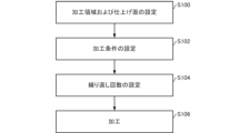
Figure 2 is a flowchart showing an example of a cross-section processing method using the focused
(1)加工領域および仕上げ面を設定する処理S100
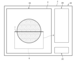
まず、ユーザーが加工領域および仕上げ面を設定する。図3は、GUI画面2を模式的に示す図である。
(1) Processing step S100 for setting the machining area and the finishing surface
First, the user sets the machining area and the finishing surface.
受付部52は、表示部62にGUI画面2を表示させる。GUI画面2には、加工領域を設定するための領域2Aが表示されている。
The
領域2Aには、試料Sの表面のSIM像4が表示されている。ユーザーは、SIM像4上で加工枠6を描くことによって加工領域を設定できる。加工枠6で囲まれたSIM像4上の領域に対応する試料Sの領域が加工領域として設定される。加工枠6は、例えば、四角形であり、大きさおよび縦横比を変更できる。
A
また、ユーザーは、SIM像4上で加工枠6の一辺を指定することによって、仕上げ面の位置を設定できる。仕上げ面は、イオンビームIBで最後に加工される面であり、加工目標となる試料Sの断面となる。仕上げ面の位置を設定することで、イオンビームIBで走査する方向が決まる。図3に示す例では、加工枠6の辺7が仕上げ面として指定されており、辺7とは反対側の辺8からイオンビームIBの走査が開始される。
The user can also set the position of the finishing surface by specifying one side of the
加工領域の設定および仕上げ面の設定は、ユーザーが操作部60を介して行う。
The user sets the machining area and the finishing surface via the
(2)加工条件を設定する処理S102
次に、ユーザーが加工条件を設定する。図4は、GUI画面2を模式的に示す図である。
(2) Processing Condition Setting Step S102
Next, the user sets the processing conditions.
GUI画面2には、加工条件を設定するための入力欄2Bが表示されている。加工条件は、1つの加工領域に対して複数設定できる。加工条件は、走査線ごとに設定できる。ここでは、イオンビームIBの照射電流Ipを設定する場合について説明する。
The
照射電流Ipは、走査線ごとに設定できる。ここで、加工領域をイオンビームIBで走査するときには、一次元的に走査線を引き、走査線を引いた方向とは垂直な方向にイオンビームIBを移動させて次の走査線を引くことを繰り返す。 The irradiation current Ip can be set for each scan line. When scanning the processing area with the ion beam IB, a scan line is drawn one-dimensionally, and the ion beam IB is moved in a direction perpendicular to the direction in which the scan line was drawn to draw the next scan line, and this process is repeated.
図4に示す例では、第1走査線L1を引いた後、第1走査線L1に垂直な方向にイオンビームIBを移動させ、第1走査線L1に平行に第2走査線L2を引く。第3走査線L3から第N走査線LNまでの走査線についても同様に走査線を引くことで、加工領域をエッチングできる。 In the example shown in FIG. 4, after drawing the first scanning line L1, the ion beam IB is moved in a direction perpendicular to the first scanning line L1, and a second scanning line L2 is drawn parallel to the first scanning line L1. By drawing scanning lines from the third scanning line L3 to the Nth scanning line LN in the same manner, the processing area can be etched.
走査線の数Nは、加工条件(照射電流(ビーム径)など)によって決まる。なお、第1走査線L1を同じ位置で複数回引いた後に、第1走査線L1に垂直な方向にイオンビームIBを移動させて第2走査線L2を複数回引いてもよい。すなわち、同じ位置で走査線を複数回引いてもよい。これにより、試料Sをより深くエッチングできる。 The number N of scanning lines is determined by the processing conditions (such as irradiation current (beam diameter)). After drawing the first scanning line L1 multiple times at the same position, the ion beam IB may be moved in a direction perpendicular to the first scanning line L1 to draw the second scanning line L2 multiple times. In other words, scanning lines may be drawn multiple times at the same position. This allows the sample S to be etched more deeply.
ユーザーが、操作部60を介して、入力欄2Bに、走査線ごとに電流量を入力することによって走査線ごとに照射電流Ipを設定できる。図4に示す例では、第1走査線L1を引くときの照射電流Ipが90nAに設定されている。また、第2走査線L2から第5走査線L5までの走査線を引くときの照射電流Ipが90nAに設定されている。また、第6走査線L6から第9走査線L9までの走査線を引くときの照射電流Ipが50nAに設定されている。また、第N-3走査線LN-3、第N-2走査線LN-2、および第N-1走査線LN-1を引くときの照射電流Ipが10nAに設定されている。また、第N走
査線LNを引くときの照射電流Ipが1nAに設定されている。
A user can set the emission current Ip for each scanning line by inputting the current amount for each scanning line in the
なお、第1走査線L1から第5走査線L5までの区間に対して、照射電流Ipとして90nAを入力することで、第1走査線L1から第5走査線L5までの区間に対して照射電流Ipを設定してもよい。このように、複数の走査線Lに対してまとめて1つの照射電流Ipを設定してもよい。 The emission current Ip may be set for the section from the first scanning line L1 to the fifth scanning line L5 by inputting 90 nA as the emission current Ip for the section from the first scanning line L1 to the fifth scanning line L5. In this way, a single emission current Ip may be set for multiple scanning lines L collectively.
上記では、加工条件として、照射電流Ipを設定する場合について説明したが、加工条件の項目は、照射電流Ipに限定されない。加工条件の項目は、照射電流Ipの他に、加工ピッチ、滞在時間(Dwell time)、加工時間、加速電圧、加工位置オフセットなどを含む。 In the above, a case where the projection current Ip is set as a processing condition has been described, but the processing condition items are not limited to the projection current Ip. In addition to the projection current Ip, the processing condition items include the processing pitch, dwell time, processing time, acceleration voltage, processing position offset, etc.
加工ピッチは、走査線を引くときの隣り合うイオンビームIBの照射点間の距離である。滞在時間は、1つの照射点あたりのイオンビームIBの滞在時間である。加工時間は、1つの走査線で走査する時間であり、加工時間として1つの走査線を引く時間の2倍の時間が設定された場合、同じ場所で走査線が2回引かれる。すなわち、第1走査線L1に対して加工時間として、第1走査線L1を引く時間の2倍の時間が設定された場合、第1走査線L1が2回引かれる。加速電圧は、イオンビームIBを加速させる電圧である。加工位置オフセットは、イオンビームIBのエッジの位置を決めるものであり、イオンビームIBの中心とイオンビームIBのエッジとの間の距離で表される。ビーム径が小さくなれば、加工位置オフセットも小さくなる。 The processing pitch is the distance between adjacent irradiation points of the ion beam IB when drawing a scan line. The residence time is the residence time of the ion beam IB per irradiation point. The processing time is the time to scan with one scan line, and if the processing time is set to twice the time to draw one scan line, the scan line is drawn twice at the same location. In other words, if the processing time for the first scan line L1 is set to twice the time to draw the first scan line L1, the first scan line L1 is drawn twice. The acceleration voltage is the voltage that accelerates the ion beam IB. The processing position offset determines the position of the edge of the ion beam IB and is expressed as the distance between the center of the ion beam IB and the edge of the ion beam IB. If the beam diameter becomes smaller, the processing position offset also becomes smaller.
上述した加工条件の各項目についても、照射電流Ipと同様に走査線Lごとに設定できる。図示はしないが、加工条件の各項目の設定は、照射電流Ipを設定する場合と同様に、操作部60を介して、入力欄に、走査線ごとに各項目の値を入力することによって行われる。
Each of the above-mentioned processing conditions can be set for each scanning line L, similar to the projection current Ip. Although not shown, each of the processing conditions is set by inputting the value of each item for each scanning line in the input field via the
(3)繰り返し回数を設定する処理S104
次に、加工を繰り返す回数を設定する。GUI画面2には、加工を繰り返す回数を設定するための入力欄2Cが表示されている。加工領域において、第1走査線L1から第N走査線LNを引くまでを加工の単位として、加工を繰り返す回数を設定する。すなわち、1回の加工は、第1走査線L1から第N走査線LNまでの走査線を引くことで行われる。ユーザーが、操作部60を介して、入力欄2Cに繰り返し回数を入力することによって繰り返し回数を設定できる。加工を繰り返すことによって、加工領域Aをより深く加工できる。
(3) Processing S104 for setting the number of repetitions
Next, the number of times the processing is repeated is set. An
(4)加工処理S106
図5は、集束イオンビーム装置100を用いた断面加工方法を説明するための図である。
(4) Processing S106
FIG. 5 is a diagram for explaining a cross-section processing method using the focused
まず、ガス銃40を用いて、加工領域Aの全体を覆うように、デポジション膜を成膜する。これにより、試料S上にデポジション膜を形成することによって試料Sを保護できる。
First, a deposition film is formed using a
次に、加工領域Aを加工する。集束イオンビーム装置100は、加工領域Aを設定する処理S100において設定された試料Sの加工領域Aを、加工条件を設定する処理S102において設定された加工条件および繰り返し回数を設定する処理S104において設定された繰り返し回数に基づいて加工する。
Next, the processing area A is processed. The focused
具体的には、光学系10が加工領域A内に第1走査線L1から第N走査線LNまでの走
査線を引くことによって、加工領域Aをエッチングする。光学系10は、第1走査線L1を引くときは、第1走査線L1に対して設定された加工条件に基づいて動作する。すなわち、光学系10は、第1走査線L1を引くときは、第1走査線L1に対して設定された、照射電流Ip、加工ピッチ、滞在時間、加工時間、加速電圧、および加工位置オフセットに従って動作する。図4に示す例では、第1走査線L1を引くときの照射電流Ipとして90nAが設定されているため、光学系10は、照射電流Ip=90nAで第1走査線L1を引く。光学系10は、その他の走査線Lを引くときについても同様に、走査線ごとに設定された加工条件に従って動作する。
Specifically, the
光学系10は、第1走査線L1から第N走査線LNまでの走査線を引く加工を処理S104で設定された回数繰り返す。
The
この結果、加工領域Aをエッチングすることができ、目的の断面を得ることができる。 As a result, the processing area A can be etched and the desired cross section can be obtained.
1.3. 処理
図6は、集束イオンビーム装置100の処理部50の断面加工処理の一例を示すフローチャートである。
1.3 Processing FIG. 6 is a flow chart showing an example of a cross-section processing process by the
ユーザーが操作部60を介して、加工領域A、仕上げ面F、加工条件、および繰り返し回数を設定すると、受付部52は、ユーザーが設定した、加工領域A、仕上げ面F、加工条件、および繰り返し回数の設定を受け付ける(S200)。
When the user sets the processing area A, the finishing surface F, the processing conditions, and the number of repetitions via the
受付部52は、ユーザーが設定した、加工領域Aの情報、仕上げ面Fの情報、および加工条件の情報を記憶部64に記憶させる。加工条件の情報は、走査線ごとに設定され、走査線ごとに記憶部64に記憶される。
The
次に、制御部54は、受付部52が受け付けた加工領域Aの情報、仕上げ面Fの情報、および加工条件の情報に基づいて、光学系10に加工領域Aを加工させる(S202)。
Next, the
制御部54は、記憶部64から第1走査線L1を引くときの光学条件を読み出し、当該光学条件に基づいて光学系10を制御する。これにより、試料S上に第1走査線L1が引かれる。同様に、制御部54は、記憶部64から第2走査線L2を引くときの光学条件を読み出し、当該光学条件に基づいて光学系10を制御する。これにより、試料S上に第2走査線L2が引かれる。制御部54は、第1走査線L1から第N走査線LNまで同様に走査線を引く。
The
例えば、図4に示すように、第5走査線L5に対して設定された照射電流Ipと第6走査線L6に対して設定された照射電流Ipが異なる場合、制御部54は、第5走査線L5を引いた後に、第6走査線L6を引く前に、光学系10に、イオンビームIBの走査を停止させて、照射電流Ipを切り替えさせる。さらに、制御部54は、照射電流Ipが切り替わったことによる、コントラストおよびブライトネスの変化を補正するためにコントラストおよびブライトネスの調整を行う。さらに、制御部54は、照射電流Ipが切り替わったことによるフォーカスのずれを補正するために、フォーカスの調整を行う。さらに、制御部54は、照射電流Ipが切り替わったことによる加工位置のずれを補正する。
For example, as shown in FIG. 4, when the irradiation current Ip set for the fifth scanning line L5 is different from the irradiation current Ip set for the sixth scanning line L6, the
制御部54は、光学系10に、第1走査線L1から第N走査線LNまでの走査線を引かせた後、設定された回数だけ加工領域Aを加工したか否かを判定する(S204)。
After causing the
制御部54は、設定された回数だけ加工領域Aを加工していないと判定した場合(S204のNo)、処理S202に戻って、光学系10に加工領域Aを加工させる(S202
)。制御部54は、設定された回数だけ加工領域Aを加工したと判定されるまで、処理S202を繰り返す。
When the
The
制御部54は、設定された回数だけ加工領域Aを加工したと判定した場合(S204のYes)、断面加工処理を終了する。
When the
1.4. 効果
集束イオンビーム装置100では、受付部52が試料Sの加工領域Aの設定、および1つの加工領域Aに対する複数の加工条件の設定を受け付け、制御部54が1つの加工領域A内に対して設定された複数の加工条件に基づいて、光学系10に加工領域AをイオンビームIBで走査させる。そのため、集束イオンビーム装置100では、1つの加工領域Aに複数の加工条件を設定できる。したがって、ユーザーは加工条件を変更するごとに加工領域Aを設定しなくてもよく、容易に複数の加工条件を設定できる。
1.4. Effects In the focused
図7は、1つの加工領域に対して1つの加工条件を設定する場合を説明するための図である。 Figure 7 is a diagram to explain the case where one processing condition is set for one processing area.
1つの加工領域に対して1つの加工条件しか設定できない場合、図7に示すように、ユーザーは加工条件を変更するごとに加工領域を設定しなければならない。これに対して、集束イオンビーム装置100では、1つの加工領域Aに対して複数の加工条件を設定できるため、1つの加工領域に対して1つの加工条件しか設定できない場合と比べて、容易に複数の加工条件を設定できる。
When only one processing condition can be set for one processing area, as shown in FIG. 7, the user must set the processing area each time the processing conditions are changed. In contrast, the focused
また、図7に示すように、1つの加工領域に対して1つの加工条件しか設定できない場合、前の加工が終わらなければ、次の加工領域および次の加工条件を設定できない。これに対して、集束イオンビーム装置100では、1つの加工領域に対して複数の加工条件を設定できるため、このような問題が生じない。例えば、集束イオンビーム装置100では、最初に加工領域および複数の加工条件を設定すれば、加工が終了するまで新たに加工領域および加工条件を設定しなくてもよい。
Also, as shown in FIG. 7, if only one processing condition can be set for one processing area, the next processing area and the next processing conditions cannot be set until the previous processing is completed. In contrast, the focused
集束イオンビーム装置100では、受付部52は走査線Lごとに加工条件の設定を受け付け、制御部54は走査線ごとに設定された加工条件に基づいて、光学系10に加工領域AをイオンビームIBで走査させる。そのため、集束イオンビーム装置100では、試料Sを加工する際に、1ラインごとに加工条件を変更できる。したがって、集束イオンビーム装置100では、加工条件を連続的に変化させることができる。
In the focused
2. 第2実施形態
2.1. 集束イオンビーム装置
次に、第2実施形態に係る集束イオンビーム装置について、図面を参照しながら説明する。図8は、第2実施形態に係る集束イオンビーム装置200の構成を示す図である。以下、第2実施形態に係る集束イオンビーム装置200において、第1実施形態に係る集束イオンビーム装置100の構成部材と同様の機能を有する部材については同一の符号を付し、その詳細な説明を省略する。
2. Second embodiment 2.1. Focused ion beam device Next, a focused ion beam device according to the second embodiment will be described with reference to the drawings. Fig. 8 is a diagram showing the configuration of a focused
上述した第1実施形態に係る集束イオンビーム装置100では、ユーザーがイオンビームIBの照射電流Ipを設定した。これに対して、第2実施形態に係る集束イオンビーム装置200では、処理部50は、イオンビームIBの照射電流Ipを設定する設定部53を含む。
In the focused
2.2. 処理
図9は、集束イオンビーム装置200の処理部50の断面加工処理の一例を示すフローチャートである。以下、上述した図6に示す処理部50の処理と異なる点について説明し、同様の点についてはその説明を省略する。
9 is a flowchart showing an example of a cross-section processing process by the
ユーザーが操作部60を介して、加工領域A、仕上げ面F、照射電流Ipを除く加工条件、および繰り返し回数を設定すると、受付部52が、ユーザーが設定した、加工領域A、仕上げ面F、照射電流を除く加工条件、および繰り返し回数の設定を受け付ける(S300)。受付部52は、受け付けた加工領域Aの情報、仕上げ面Fの情報、照射電流を除く加工条件の情報、および繰り返し回数の情報を記憶部64に記憶させる。
When the user sets the processing area A, the finishing surface F, the processing conditions excluding the irradiation current Ip, and the number of repetitions via the
次に、設定部53は、走査線ごとに照射電流Ipを設定する(S302)。照射電流Ipを設定する処理については後述する。受付部52は、設定部53による照射電流Ipの設定を受け付ける(S303)。
Next, the setting
次に、制御部54は、受付部52が受け付けた加工領域Aの情報、仕上げ面Fの情報、および照射電流Ipを含む加工条件の情報に基づいて、光学系10に加工領域Aを加工させる(S304)。
Next, the
制御部54は、記憶部64から第1走査線L1を引くときの光学条件を読み出し、当該光学条件に基づいて光学系10を制御する。これにより、試料S上に第1走査線L1が引かれる。同様に、制御部54は、記憶部64から第2走査線L2を引くときの光学条件を読み出し、当該光学条件に基づいて光学系10を制御する。これにより、試料S上に第2走査線L2が引かれる。制御部54は、第1走査線L1から第N走査線LNまで同様の処理を繰り返す。
The
制御部54は、光学系10に、第1走査線L1から第N走査線LNまでの走査線を引かせた後、設定された回数だけ加工領域Aを加工したか否かを判定する(S306)。
After causing the
制御部54は、設定された回数だけ加工領域Aを加工していないと判定した場合(S306のNo)、処理S304に戻って、加工領域Aの情報、仕上げ面Fの情報、および加工条件の情報に基づいて、光学系10に加工領域Aを加工させる(S304)。制御部54は、設定された回数だけ加工領域Aを加工したと判定されるまで、処理S304を繰り返す。
When the
制御部54は、設定された回数だけ加工領域Aを加工したと判定した場合(S306のYes)、断面加工処理を終了する。
When the
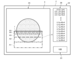
図10は、照射電流Ipを設定する処理S302の一例を示すフローチャートである。図11~図13は、照射電流Ipの設定方法を説明するための図である。 Figure 10 is a flowchart showing an example of process S302 for setting the emission current Ip. Figures 11 to 13 are diagrams for explaining a method for setting the emission current Ip.
設定部53は、まず、図11に示すように、設定された加工領域Aに基づいて、第1照射電流Ip-1を設定する(S400)。
First, the setting
第1照射電流Ip-1は、加工領域Aを加工する際に用いるイオンビームIBの照射電流Ipのうちの最大の照射電流である。 The first irradiation current Ip-1 is the maximum irradiation current among the irradiation currents Ip of the ion beam IB used when processing the processing area A.
設定部53は、例えば、加工領域Aの加工幅Wに基づいて、第1照射電流Ip-1を設定する。加工幅Wは、加工領域Aの走査線Lを引く方向の大きさである。設定部53は、加工幅Wが大きいほど、第1照射電流Ip-1を大きく設定する。加工幅Wに基づいて第1照射電流Ip-1を設定することによって、加工幅Wが大きいほど大きな照射電流で加
工することができ、短時間に効率よく加工領域Aを加工できる。
The setting
例えば、下記の条件式(1)を満たす照射電流のうちの最大の照射電流を第1照射電流Ip-1として設定する。 For example, the maximum emission current among the emission currents that satisfy the following conditional expression (1) is set as the first emission current Ip-1.
(W/D)>100 ・・・(1)
ここで、Wは加工幅であり、DはイオンビームIBのビーム径(直径)である。イオンビームIBのビーム径Dは、照射電流Ipに対応している。照射電流Ipが大きいほど、ビーム径Dが大きくなる。
(W/D)>100...(1)
Here, W is the processing width, and D is the beam diameter of the ion beam IB. The beam diameter D of the ion beam IB corresponds to the irradiation current Ip. The larger the irradiation current Ip, the The diameter D becomes larger.
記憶部64には、ビーム径と照射電流Ipを関連づけるテーブルが記憶されている。設定部53は、当該テーブルを用いて、上記条件式(1)を満たすビーム径から照射電流Ipを求めてもよい。なお、記憶部64には、ビーム径と照射電流Ipを関連づける関係式が記憶されており、設定部53は当該関係式を用いて上記条件式(1)を満たすビーム径から照射電流Ipを求めてもよい。
The
なお、第1照射電流Ip-1を求める方法は、上記の例に限定されず、例えば、設定された加工領域Aの面積に基づいて第1照射電流Ip-1を設定してもよい。すなわち、加工領域Aの面積が大きいほど、第1照射電流Ip-1を大きく設定してもよい。設定部53は、記憶部64に記憶された加工領域Aの面積と第1照射電流Ip-1を関連付けるテーブルまたは関係式を用いて、加工領域Aの面積から第1照射電流Ip-1を求めてもよい。加工領域Aの面積に基づいて第1照射電流Ip-1を設定することによって、加工領域Aの面積が大きいほど大きな照射電流で加工することができ、短時間に効率よく加工領域Aを加工できる。また、例えば、設定された加工領域Aの走査線Lを引く方向と垂直な方向の大きさに基づいて最大照射電流を設定してもよい。
The method of calculating the first emission current Ip-1 is not limited to the above example, and the first emission current Ip-1 may be set based on the area of the set processing area A. That is, the larger the area of the processing area A, the larger the first emission current Ip-1 may be set. The setting
次に、設定部53は、第1照射電流Ip-1で加工する第1領域A1を設定する(S402)。
Next, the setting
設定部53は、第1照射電流Ip-1に基づいて、第1照射電流Ip-1で加工する第1領域A1を設定する。設定部53は、第1照射電流Ip-1が大きいほど仕上げ面Fとの間の距離D1が大きくなるように第1領域A1を設定する。距離D1は、走査線Lを引く方向と垂直な方向における、仕上げ面Fと第1領域A1との間の最短距離である。
The setting
例えば、記憶部64には、照射電流Ipと、当該照射電流Ipで加工したときに仕上げ面Fにダメージを与えない距離と、が関連づけられたテーブルが記憶されている。設定部53は、当該テーブルを参照して、第1照射電流Ip-1から距離D1の情報を取得する。設定部53は、取得した距離D1の情報に基づいて第1領域A1を設定する。すなわち、設定部53は、加工領域Aのうちの仕上げ面Fから距離D1以上離れた領域を第1領域A1として設定する。
For example, the
第1照射電流Ip-1に基づいて第1領域A1を設定することによって、仕上げ面Fに対するイオンビームIBによるダメージを低減しつつ、加工時間を短くできる。 By setting the first area A1 based on the first irradiation current Ip-1, the processing time can be shortened while reducing damage caused by the ion beam IB to the finishing surface F.
設定部53は、第1照射電流Ip-1(ビーム径)および第1領域A1の走査線Lを引く方向とは垂直な方向の大きさに基づいて、第1領域A1における走査線Lの数を設定する。
The setting
図11に示す例では、第1領域A1における走査線Lの数は5本であり、第1領域A1において第1走査線L1から第5走査線L5までの走査線が引かれる。第1走査線L1か
ら第5走査線L5までの各走査線に対して、第1照射電流Ip-1として80nAが設定されている。
11, the number of scanning lines L in the first region A1 is five, and scanning lines from the first scanning line L1 to the fifth scanning line L5 are drawn in the first region A1. A first emission current Ip-1 of 80 nA is set for each of the scanning lines from the first scanning line L1 to the fifth scanning line L5.
なお、ここでは、第1領域A1を設定するためのパラメーターとして、照射電流を用いたが、第1領域A1を設定するためのパラメーターは、ビーム径に基づく値であればよい。 Here, the irradiation current is used as the parameter for setting the first region A1, but the parameter for setting the first region A1 may be any value based on the beam diameter.
次に、設定部53は、図12に示すように、第1領域A1の次に加工する第2領域A2における第2照射電流Ip-2を設定する(S404)。
Next, the setting
設定部53は、第1照射電流Ip-1に基づいて、第2照射電流Ip-2を設定する。設定部53は、第2照射電流Ip-2を、第1照射電流Ip-1よりも少ない電流量に設定する。例えば、設定部53は、第1照射電流Ip-1で得られるビーム径の1/2のビーム径が得られる照射電流を、第2照射電流Ip-2と設定する。なお、設定部53は、第1照射電流Ip-1で得られるビーム径の1/4のビーム径が得られる照射電流を第2照射電流Ip-2として設定してもよい。
The setting
次に、設定部53は、第2照射電流Ip-2で加工する第2領域A2を設定する(S406)。
Next, the setting
設定部53は、第1領域A1を設定する方法と同様の方法で第2領域A2を設定する。すなわち、設定部53は、第2照射電流Ip-2に基づいて、第2領域A2を設定する。設定部53は、第2照射電流Ip-2が大きいほど仕上げ面Fとの間の距離D2が大きくなるように第2領域A2を設定する。
The setting
設定部53は、第2照射電流Ip-2(ビーム径)および第2領域A2の走査線Lを引く方向とは垂直な方向の大きさに基づいて、第2領域A2における走査線Lの数を設定する。
The setting
設定部53は、照射電流Ipと、当該照射電流Ipで加工したときに仕上げ面Fにダメージを与えない距離と、が関連付けられたテーブルを参照して、第2照射電流Ip-2から距離D2の情報を取得する。設定部53は、取得した距離D2の情報に基づいて第2領域A2を設定する。すなわち、設定部53は、加工領域Aのうちの仕上げ面Fから距離D2以上離れた領域であって、第1領域A1を除いた領域を第2領域A2として設定する。
The setting
図12に示す例では、第2領域A2における走査線Lの数は4本であり、第2領域A2において第6走査線L6から第9走査線L9までの走査線が引かれる。第6走査線L6から第9走査線L9までの各走査線に対して、第2照射電流Ip-2として40nAが設定されている。 In the example shown in FIG. 12, the number of scanning lines L in the second region A2 is four, and scanning lines from the sixth scanning line L6 to the ninth scanning line L9 are drawn in the second region A2. For each of the scanning lines from the sixth scanning line L6 to the ninth scanning line L9, the second irradiation current Ip-2 is set to 40 nA.
設定部53は、第2照射電流Ip-2が仕上げ面Fを加工するときの加工条件を満たすか否かを判定する(S408)。
The setting
設定部53は、例えば、以下の条件式(2)を満たした場合に、第2照射電流Ip-2を、仕上げ面Fの加工条件を満たすと判定する。
The setting
(W/D)>2000 ・・・(2)
設定部53は、加工幅Wに対してビーム径Dが十分に小さくなった場合に、仕上げ面Fを加工できる照射電流Ipとなったと判定する。上記の条件式(2)では、ビーム径Dが加工幅Wの1/2000未満となった場合に、仕上げ面Fの加工条件を満たすと判定され
る。
(W/D)>2000...(2)
The setting
設定部53は、第2照射電流Ip-2が仕上げ面Fを加工するときの加工条件を満たさないと判定した場合(S410のNo)、処理S404に戻って、第2照射電流Ip-2に基づいて第3照射電流Ip-3を設定する(S404)。第3照射電流Ip-3は、第2照射電流Ip-2を設定する場合と同様に、第2照射電流Ip-2で得られるビーム径の1/2のビーム径が得られる照射電流に設定される。
When the
次に、設定部53は、第3照射電流Ip-3に基づいて、第3照射電流Ip-3で加工する第3領域A3を設定する(S406)。第3領域A3は、第2領域A2を設定する場合と同様に、第3照射電流Ip-3(第3照射電流Ip-3で得られるビーム径)に基づいて設定される。
Next, the setting
次に、設定部53は、第3照射電流Ip-3が仕上げ面Fを加工するときの加工条件を満たすか否かを判定する(S408)。このように、設定部53は、照射電流Ipが仕上げ面Fを加工するときの加工条件を満たすまで、処理S404、処理S406、処理S408、および処理S410を繰り返す。
Next, the setting
すなわち、設定部53は、図13に示すように、第M照射電流Ip-M(Mは2以上N以下の整数)を第M-1照射電流Ip-(M-1)で得られるビーム径の1/2のビーム径が得られる照射電流に設定し(S404)、第M領域AMを第M照射電流Ip-M(第M照射電流Ip-Mで得られるビーム径)に基づいて設定する(S406)。
That is, as shown in FIG. 13, the setting
設定部53は、第M照射電流Ip-Mが仕上げ面Fを加工するときの加工条件を満たすと判定した場合(S410のYes)、照射電流を設定する処理を終了する。
When the
以上の処理により、走査線Lごとに照射電流Ipを設定できる。 By performing the above process, the irradiation current Ip can be set for each scanning line L.
なお、上記の条件式(2)では、ビーム径Dの上限を設定しているが、ビーム径Dの上限および下限を設定してもよい。例えば、第M照射電流Ip-Mを設定した後、仕上げ面Fの加工条件を満たすか否かを判定する処理S408において、下記の条件式(3)を満たした場合に仕上げ面Fの加工条件を満たすと判定してもよい。 In the above conditional formula (2), an upper limit for the beam diameter D is set, but upper and lower limits for the beam diameter D may be set. For example, after setting the Mth irradiation current Ip-M, in process S408 for determining whether the machining conditions for the finishing surface F are satisfied, it may be determined that the machining conditions for the finishing surface F are satisfied if the following conditional formula (3) is satisfied.
2000<(W/D)<10000 ・・・(3)
なお、第M照射電流Ip-Mで得られるビーム径が加工幅Wの1/10000以下になった場合には、設定部53は、第M照射電流Ip-Mを、関係式(3)を満たすビーム径Dが得られる電流量に設定し、照射電流Ipを設定する処理を終了する。
2000<(W/D)<10000...(3)
In addition, when the beam diameter obtained by the Mth irradiation current Ip-M becomes 1/10000 or less of the processing width W, the setting
2.3. 効果
集束イオンビーム装置200は、イオンビームIBの照射電流Ipを設定する設定部53を含み、設定部53は、設定された加工領域Aに基づいて、イオンビームIBの最大照射電流である第1照射電流Ip-1を設定する。そのため、集束イオンビーム装置200では、ユーザーが最大照射電流を設定する手間を省くことができる。
2.3 Effects The focused
集束イオンビーム装置200では、加工領域Aの加工幅Wに基づいて、第1照射電流Ip-1を設定する。そのため、集束イオンビーム装置200では、ユーザーが最大照射電流を設定する手間を省くことができる。
In the focused
また、集束イオンビーム装置200では、加工領域Aの面積に基づいて、第1照射電流Ip-1を設定してもよい。そのため、集束イオンビーム装置200では、ユーザーが最
大照射電流を設定する手間を省くことができる。
Furthermore, in the focused
集束イオンビーム装置200では、設定部53は、第1照射電流Ip-1に基づいて、加工領域Aのうちの第1照射電流Ip-1で加工する第1領域A1を設定する。そのため、集束イオンビーム装置200では、ユーザーが最大照射電流で加工する第1領域A1を設定する手間を省くことができる。
In the focused
集束イオンビーム装置200では、設定部53は、第1照射電流Ip-1に基づいて、第1領域A1の次に加工する第2領域A2における第2照射電流Ip-2を設定し、第2照射電流Ip-2に基づいて第2領域A2を設定する。また、集束イオンビーム装置200では、受付部52は、加工目標となる試料Sの断面の位置である仕上げ面Fの設定を受け付ける。設定部53は、加工目標となる試料Sの断面と第2領域A2との間の距離D2が、仕上げ面Fと第1領域A1との間の距離D1よりも小さくなるように、第2領域A2を設定する。そのため、集束イオンビーム装置200では、ユーザーが第2照射電流Ip-2で加工する第2領域A2を設定する手間を省くことができる。
In the focused
このように集束イオンビーム装置200では、照射電流Ipが自動で設定されるため、集束イオンビーム装置200の能力についての知識がなくても、作製したい断面に適した加工条件を設定できる。
In this way, the focused
2.4. 変形例
上述した図10に示す照射電流Ipを設定する処理S302では、設定部53が加工領域Aの加工幅Wに基づいて第1照射電流Ip-1を設定した(S400)。これに対して、設定部53は、第1照射電流Ip-1の複数の候補を提示し、ユーザーによる候補の選択を受け付けることによって、第1照射電流Ip-1を設定する。
10, the setting
設定部53は、第1照射電流Ip-1の候補として、上述した条件式(1)を満たす照射電流から複数の候補を提示する。
The setting
設定部53は、例えば、条件式(1)を満たすビーム径Dのうちの最大のビーム径Dが得られる照射電流を第1照射電流Ip-1の第1候補とし、第1候補からあらかじめ設定された割合だけ照射電流を減少させた照射電流を第2候補とし、第2候補からあらかじめ設定された割合だけ照射電流を減少させた照射電流を第3候補とする。第1候補、第2候補、および第3候補は、表示部62に表示される。
The setting
なお、候補を列挙する方法は特に限定されず、条件式(1)を満たすビーム径Dのうちの最大のビーム径Dが得られる照射電流を第1照射電流Ip-1の第1候補とし、第1候補からあらかじめ設定された割合だけ電流量を上昇させた照射電流を第2候補とし、第1候補からあらかじめ設定された割合だけ電流量を減少させた照射電流を第3候補としてもよい。また、候補を列挙する数も特に限定されず、候補の数は3以上であってもよい。 The method of listing the candidates is not particularly limited, and the irradiation current that produces the largest beam diameter D among the beam diameters D that satisfy conditional formula (1) may be set as the first candidate for the first irradiation current Ip-1, an irradiation current whose current amount is increased from the first candidate by a preset percentage may be set as the second candidate, and an irradiation current whose current amount is decreased from the first candidate by a preset percentage may be set as the third candidate. In addition, the number of candidates to be listed is not particularly limited, and the number of candidates may be three or more.
ユーザーは、提示された複数の候補のなかから1つの候補を選択する。ユーザーは、操作部60を介して、複数の候補のなかから1つを選択できる。設定部53は、操作部60を介して、ユーザーによる候補の選択を受け付ける。これにより、第1照射電流Ip-1が設定される。
The user selects one candidate from among the multiple candidates presented. The user can select one from among the multiple candidates via the
このように、設定部53が提示した第1照射電流Ip-1の複数の候補からユーザーが1つを選択することによって、第1照射電流Ip-1を設定できる。
In this way, the user can set the first emission current Ip-1 by selecting one from multiple candidates for the first emission current Ip-1 presented by the setting
なお、設定部53は、第M照射電流Ip-M(ただしMは2以上N以下の整数)を設定
する処理S404についても同様に、複数の候補を提示し、ユーザーによる候補の選択を受け付けることによって第M照射電流Ip-Mを設定してもよい。
Similarly, for process S404 of setting the Mth irradiation current Ip-M (where M is an integer greater than or equal to 2 and less than or equal to N), the setting
例えば、設定部53は、第M照射電流Ip-Mの候補として、第M-1照射電流Ip-(M-1)で得られるビーム径の1/2のビーム径が得られる照射電流を第1候補とし、第M-1照射電流Ip-(M-1)で得られるビーム径の1/4のビーム径が得られる照射電流を第2候補とし、第M-1照射電流Ip-(M-1)で得られるビーム径の1/8のビーム径が得られる照射電流を第3候補としてもよい。
For example, as candidates for the Mth irradiation current Ip-M, the setting
3. 変形例
なお、本発明は上述した実施形態に限定されず、本発明の要旨の範囲内で種々の変形実施が可能である。
3. Modifications The present invention is not limited to the above-described embodiment, and various modifications can be made within the scope of the present invention.
例えば、上述した第2実施形態では、設定部53が照射電流Ipを設定する場合について説明したが、設定部53は加速電圧を設定してもよい。
For example, in the second embodiment described above, the setting
加速電圧も照射電流Ipと同様にビーム径Dに対応するため、設定部53は、第1照射電流Ip-1を設定する場合と同様に、加工領域Aに基づいて最大加速電圧である第1加速電圧を設定してもよい。また、設定部53は、設定された第1加速電圧に基づいて第2領域A2を加工するときの第2加速電圧を設定してもよい。
Since the acceleration voltage also corresponds to the beam diameter D, like the irradiation current Ip, the setting
このように、設定部53は、照射電流Ipを設定する場合と同様に、加速電圧を設定してもよい。
In this way, the setting
本発明は、上述した実施形態に限定されるものではなく、さらに種々の変形が可能である。例えば、本発明は、実施形態で説明した構成と実質的に同一の構成を含む。実質的に同一の構成とは、例えば、機能、方法、及び結果が同一の構成、あるいは目的及び効果が同一の構成である。また、本発明は、実施形態で説明した構成の本質的でない部分を置き換えた構成を含む。また、本発明は、実施形態で説明した構成と同一の作用効果を奏する構成又は同一の目的を達成することができる構成を含む。また、本発明は、実施形態で説明した構成に公知技術を付加した構成を含む。 The present invention is not limited to the above-described embodiments, and various modifications are possible. For example, the present invention includes configurations that are substantially the same as the configurations described in the embodiments. Substantially the same configurations are, for example, configurations that have the same functions, methods, and results, or configurations that have the same purpose and effect. The present invention also includes configurations in which non-essential parts of the configurations described in the embodiments are replaced. The present invention also includes configurations that have the same effects as the configurations described in the embodiments, or that can achieve the same purpose. The present invention also includes configurations in which publicly known technology is added to the configurations described in the embodiments.
2…GUI画面、2A…領域、2B…入力欄、2C…入力欄、4…SIM像、6…加工枠、7…辺、8…辺、10…光学系、11…イオン源、12…引出電極、13…加速電極、14…集束レンズ、15…ビームブランキング電極、16…可変マルチアパーチャー、17…ビーム偏向電極、18…対物レンズ、20…試料ステージ、30…二次電子検出器、40…ガス銃、50…処理部、52…受付部、53…設定部、54…制御部、60…操作部、62…表示部、64…記憶部、100…集束イオンビーム装置、200…集束イオンビーム装置 2...GUI screen, 2A...area, 2B...input field, 2C...input field, 4...SIM image, 6...processing frame, 7...side, 8...side, 10...optical system, 11...ion source, 12...extraction electrode, 13...acceleration electrode, 14...focusing lens, 15...beam blanking electrode, 16...variable multi-aperture, 17...beam deflection electrode, 18...objective lens, 20...sample stage, 30...secondary electron detector, 40...gas gun, 50...processing unit, 52...reception unit, 53...setting unit, 54...control unit, 60...operation unit, 62...display unit, 64...storage unit, 100...focused ion beam device, 200...focused ion beam device
Claims (8)
前記試料を前記イオンビームで走査する光学系と、
前記試料の加工領域の設定、および1つの前記加工領域に対する複数の加工条件の設定を受け付ける受付部と、
前記光学系を制御する制御部と、
を含み、
前記制御部は、1つの前記加工領域内に対して設定された複数の加工条件に基づいて、前記光学系に前記加工領域を前記イオンビームで走査させ、
前記受付部は、前記加工領域を前記イオンビームで走査するときの走査線ごとに加工条件の設定を受け付け、
前記制御部は、走査線ごとに設定された加工条件に基づいて、前記光学系に前記加工領域を前記イオンビームで走査させる、集束イオンビーム装置。 1. A focused ion beam apparatus for processing a cross section of a sample by scanning the sample with an ion beam, comprising:
an optical system for scanning the sample with the ion beam;
A reception unit that receives a setting of a processing area of the sample and a setting of a plurality of processing conditions for one of the processing areas;
A control unit that controls the optical system;
Including,
The control unit causes the optical system to scan the processing region with the ion beam based on a plurality of processing conditions set for one of the processing regions ;
the reception unit receives settings of processing conditions for each scanning line when scanning the processing region with the ion beam;
The control unit is a focused ion beam device that causes the optical system to scan the processing region with the ion beam based on processing conditions set for each scanning line .
前記試料を前記イオンビームで走査する光学系と、
前記試料の加工領域の設定、および1つの前記加工領域に対する複数の加工条件の設定を受け付ける受付部と、
前記光学系を制御する制御部と、
前記加工条件を設定する設定部と、
を含み、
前記制御部は、1つの前記加工領域内に対して設定された複数の加工条件に基づいて、前記光学系に前記加工領域を前記イオンビームで走査させ、
前記加工条件は、前記イオンビームの照射電流を含み、
前記設定部は、設定された前記加工領域に基づいて、前記イオンビームの最大照射電流である第1照射電流を設定する、集束イオンビーム装置。 1. A focused ion beam apparatus for processing a cross section of a sample by scanning the sample with an ion beam, comprising:
an optical system for scanning the sample with the ion beam;
A reception unit that receives a setting of a processing area of the sample and a setting of a plurality of processing conditions for one of the processing areas;
A control unit that controls the optical system;
A setting unit for setting the processing conditions;
Including,
The control unit causes the optical system to scan the processing region with the ion beam based on a plurality of processing conditions set for one of the processing regions ;
the processing conditions include a irradiation current of the ion beam,
The focused ion beam device , wherein the setting unit sets a first irradiation current that is a maximum irradiation current of the ion beam based on the set processing area .
前記加工条件は、前記イオンビームの照射電流を含む、集束イオンビーム装置。 In claim 1,
A focused ion beam apparatus, wherein the processing conditions include an irradiation current of the ion beam.
前記設定部は、前記加工領域の走査線を引く方向の大きさに基づいて、前記第1照射電流を設定する、集束イオンビーム装置。 In claim 2 ,
The setting unit sets the first irradiation current based on a size of the processing area in a direction in which a scan line is drawn.
前記設定部は、前記加工領域の面積に基づいて、前記第1照射電流を設定する、集束イオンビーム装置。 In claim 2 ,
The setting unit sets the first irradiation current based on an area of the processing region.
前記設定部は、前記第1照射電流に基づいて、前記加工領域のうちの前記第1照射電流で加工する第1領域を設定する、集束イオンビーム装置。 In claim 2 ,
The setting unit sets a first region to be processed with the first irradiation current in the processing region based on the first irradiation current.
前記設定部は、
前記第1照射電流に基づいて、前記第1領域の次に加工する第2領域における第2照射電流を設定し、
前記第2照射電流に基づいて、前記第2領域を設定する、集束イオンビーム装置。 In claim 6 ,
The setting unit is
A second irradiation current in a second region to be processed next to the first region is set based on the first irradiation current;
A focused ion beam device that sets the second area based on the second irradiation current.
前記受付部は、加工目標となる前記試料の断面の位置の設定を受け付け、
前記設定部は、加工目標となる前記試料の断面と前記第2領域との間の距離が、加工目標となる前記試料の断面と前記第1領域との間の距離よりも小さくなるように、前記第2領域を設定する、集束イオンビーム装置。 In claim 7 ,
The receiving unit receives a setting of a position of a cross section of the sample that is to be processed,
A focused ion beam device, wherein the setting unit sets the second region so that a distance between a cross-section of the sample to be processed and the second region is smaller than a distance between a cross-section of the sample to be processed and the first region.
Priority Applications (3)
| Application Number | Priority Date | Filing Date | Title |
|---|---|---|---|
| JP2022136135A JP7586866B2 (en) | 2022-08-29 | 2022-08-29 | Focused Ion Beam Equipment |
| US18/238,715 US20240071718A1 (en) | 2022-08-29 | 2023-08-28 | Focused Ion Beam Apparatus |
| EP23193877.0A EP4333021A3 (en) | 2022-08-29 | 2023-08-29 | Focused ion beam apparatus |
Applications Claiming Priority (1)
| Application Number | Priority Date | Filing Date | Title |
|---|---|---|---|
| JP2022136135A JP7586866B2 (en) | 2022-08-29 | 2022-08-29 | Focused Ion Beam Equipment |
Publications (2)
| Publication Number | Publication Date |
|---|---|
| JP2024032464A JP2024032464A (en) | 2024-03-12 |
| JP7586866B2 true JP7586866B2 (en) | 2024-11-19 |
Family
ID=87863508
Family Applications (1)
| Application Number | Title | Priority Date | Filing Date |
|---|---|---|---|
| JP2022136135A Active JP7586866B2 (en) | 2022-08-29 | 2022-08-29 | Focused Ion Beam Equipment |
Country Status (3)
| Country | Link |
|---|---|
| US (1) | US20240071718A1 (en) |
| EP (1) | EP4333021A3 (en) |
| JP (1) | JP7586866B2 (en) |
Citations (3)
| Publication number | Priority date | Publication date | Assignee | Title |
|---|---|---|---|---|
| JP2005108472A (en) | 2003-09-29 | 2005-04-21 | Hitachi Ltd | Method of forming film using charged particle beam, selective etching method, and charged particle beam apparatus |
| JP2006164792A (en) | 2004-12-08 | 2006-06-22 | Jeol Ltd | Sample processing method |
| JP2006313704A (en) | 2005-05-09 | 2006-11-16 | Jeol Ltd | Focused ion beam device |
Family Cites Families (2)
| Publication number | Priority date | Publication date | Assignee | Title |
|---|---|---|---|---|
| JP3060613B2 (en) * | 1991-07-12 | 2000-07-10 | 株式会社日立製作所 | Focused ion beam apparatus and cross-section processing method using focused ion beam |
| JPH11260307A (en) * | 1998-03-12 | 1999-09-24 | Jeol Ltd | Focused ion beam equipment |
-
2022
- 2022-08-29 JP JP2022136135A patent/JP7586866B2/en active Active
-
2023
- 2023-08-28 US US18/238,715 patent/US20240071718A1/en active Pending
- 2023-08-29 EP EP23193877.0A patent/EP4333021A3/en active Pending
Patent Citations (3)
| Publication number | Priority date | Publication date | Assignee | Title |
|---|---|---|---|---|
| JP2005108472A (en) | 2003-09-29 | 2005-04-21 | Hitachi Ltd | Method of forming film using charged particle beam, selective etching method, and charged particle beam apparatus |
| JP2006164792A (en) | 2004-12-08 | 2006-06-22 | Jeol Ltd | Sample processing method |
| JP2006313704A (en) | 2005-05-09 | 2006-11-16 | Jeol Ltd | Focused ion beam device |
Also Published As
| Publication number | Publication date |
|---|---|
| JP2024032464A (en) | 2024-03-12 |
| EP4333021A3 (en) | 2024-03-13 |
| EP4333021A2 (en) | 2024-03-06 |
| US20240071718A1 (en) | 2024-02-29 |
Similar Documents
| Publication | Publication Date | Title |
|---|---|---|
| US20100181478A1 (en) | Charged particle beam adjusting method and charged particle beam apparatus | |
| JP4563049B2 (en) | Ion beam processing method using FIB-SEM composite apparatus | |
| CN104040676B (en) | Charged particle line apparatus and oblique view method for displaying image | |
| US6118122A (en) | Ion beam working apparatus | |
| JP4194526B2 (en) | Charged particle beam adjustment method and charged particle beam apparatus | |
| JP5247761B2 (en) | FIB-SEM combined device | |
| JP6953324B2 (en) | Scanning electron microscope autofocus method | |
| JP7586866B2 (en) | Focused Ion Beam Equipment | |
| JP6266312B2 (en) | Focused ion beam apparatus and ion beam focus adjustment method | |
| US7528394B2 (en) | Focused ion beam system | |
| US11676796B2 (en) | Charged particle beam device | |
| US20190006145A1 (en) | Method of verifying operation parameter of scanning electron microscope | |
| JP2005005055A (en) | Sample height information acquisition method | |
| JP6814109B2 (en) | Microstructure processing method and microstructure processing equipment | |
| JP4829584B2 (en) | Method for automatically adjusting electron beam apparatus and electron beam apparatus | |
| JP7271717B2 (en) | Incident angle adjustment mechanism to charged particle beam diaphragm and charged particle beam device | |
| JP2013114893A (en) | Scanning electron microscope, and automatic focusing method for the same | |
| JP7698796B2 (en) | Charged Particle Beam System | |
| JP2012114014A (en) | Charged beam device, and image display method of charged beam device | |
| JP7208212B2 (en) | Transmission Electron Microscope and Optical System Adjustment Method | |
| JPH11260307A (en) | Focused ion beam equipment | |
| JPH10302704A (en) | Charged particle beam equipment | |
| JP2017162606A (en) | Axial alignment method and electro microscope | |
| WO2024142368A1 (en) | Charged particle beam device and method for adjusting charged particle beam device | |
| JP2007109560A (en) | Focused ion beam apparatus and processing position setting method of focused ion beam apparatus |
Legal Events
| Date | Code | Title | Description |
|---|---|---|---|
| A621 | Written request for application examination |
Free format text: JAPANESE INTERMEDIATE CODE: A621 Effective date: 20231206 |
|
| A977 | Report on retrieval |
Free format text: JAPANESE INTERMEDIATE CODE: A971007 Effective date: 20240710 |
|
| A131 | Notification of reasons for refusal |
Free format text: JAPANESE INTERMEDIATE CODE: A131 Effective date: 20240716 |
|
| A521 | Request for written amendment filed |
Free format text: JAPANESE INTERMEDIATE CODE: A523 Effective date: 20240905 |
|
| TRDD | Decision of grant or rejection written | ||
| A01 | Written decision to grant a patent or to grant a registration (utility model) |
Free format text: JAPANESE INTERMEDIATE CODE: A01 Effective date: 20241029 |
|
| A61 | First payment of annual fees (during grant procedure) |
Free format text: JAPANESE INTERMEDIATE CODE: A61 Effective date: 20241107 |
|
| R150 | Certificate of patent or registration of utility model |
Ref document number: 7586866 Country of ref document: JP Free format text: JAPANESE INTERMEDIATE CODE: R150 |