JP7583000B2 - Computer and data processing method - Google Patents
Computer and data processing method Download PDFInfo
- Publication number
- JP7583000B2 JP7583000B2 JP2022141346A JP2022141346A JP7583000B2 JP 7583000 B2 JP7583000 B2 JP 7583000B2 JP 2022141346 A JP2022141346 A JP 2022141346A JP 2022141346 A JP2022141346 A JP 2022141346A JP 7583000 B2 JP7583000 B2 JP 7583000B2
- Authority
- JP
- Japan
- Prior art keywords
- data
- register
- encrypted
- processor
- user data
- Prior art date
- Legal status (The legal status is an assumption and is not a legal conclusion. Google has not performed a legal analysis and makes no representation as to the accuracy of the status listed.)
- Active
Links
Images


Classifications
-
- G—PHYSICS
- G06—COMPUTING OR CALCULATING; COUNTING
- G06F—ELECTRIC DIGITAL DATA PROCESSING
- G06F21/00—Security arrangements for protecting computers, components thereof, programs or data against unauthorised activity
- G06F21/60—Protecting data
- G06F21/602—Providing cryptographic facilities or services
-
- G—PHYSICS
- G06—COMPUTING OR CALCULATING; COUNTING
- G06F—ELECTRIC DIGITAL DATA PROCESSING
- G06F21/00—Security arrangements for protecting computers, components thereof, programs or data against unauthorised activity
- G06F21/60—Protecting data
- G06F21/64—Protecting data integrity, e.g. using checksums, certificates or signatures
-
- G—PHYSICS
- G06—COMPUTING OR CALCULATING; COUNTING
- G06F—ELECTRIC DIGITAL DATA PROCESSING
- G06F21/00—Security arrangements for protecting computers, components thereof, programs or data against unauthorised activity
- G06F21/70—Protecting specific internal or peripheral components, in which the protection of a component leads to protection of the entire computer
- G06F21/78—Protecting specific internal or peripheral components, in which the protection of a component leads to protection of the entire computer to assure secure storage of data
Landscapes
- Engineering & Computer Science (AREA)
- Theoretical Computer Science (AREA)
- Computer Security & Cryptography (AREA)
- Computer Hardware Design (AREA)
- Software Systems (AREA)
- Physics & Mathematics (AREA)
- General Engineering & Computer Science (AREA)
- General Physics & Mathematics (AREA)
- General Health & Medical Sciences (AREA)
- Health & Medical Sciences (AREA)
- Bioethics (AREA)
- Signal Processing For Digital Recording And Reproducing (AREA)
- Storage Device Security (AREA)
Description
本発明は、ユーザデータの暗号化及び復号の技術に関する。 The present invention relates to technology for encrypting and decrypting user data.
内蔵されている記憶媒体からユーザデータが不正に読み出されないように、ユーザデータを暗号化して保存する機能を有するストレージシステムがある。前述の機能を有するストレージシステムは、ライトコマンドに応じて、外部のホストコンピュータから入力されたユーザデータを暗号化し、暗号化されたユーザデータを記憶媒体に保存する。また、前述の機能を有するストレージシステムは、リードコマンドに応じて、記憶媒体に保存された暗号化されたユーザデータを復号し、ユーザデータを出力する。 There is a storage system that has the function of encrypting and storing user data to prevent unauthorized reading of the user data from the built-in storage medium. In response to a write command, the storage system with the above-mentioned function encrypts user data input from an external host computer and stores the encrypted user data in the storage medium. In response to a read command, the storage system with the above-mentioned function decrypts the encrypted user data stored in the storage medium and outputs the user data.
ストレージシステムがデータの暗号化及び復号を支援するハードウェアを有していない場合、ストレージシステムが備えるCPUが、複数のCPU命令で構成されたプログラムコードにしたがって、ライト処理に伴うユーザデータの暗号化及びリード処理に伴う暗号化ユーザデータの復号を実行する。ストレージシステムのCPUの暗号化及び復号の処理性能が高いほうが、ユーザデータの読み書きのレスポンスが高くなる。 If the storage system does not have hardware to support data encryption and decryption, the CPU in the storage system performs encryption of user data associated with write processing and decryption of encrypted user data associated with read processing in accordance with program code consisting of multiple CPU instructions. The higher the encryption and decryption processing performance of the storage system's CPU, the higher the response time for reading and writing user data.
暗号化及び復号の処理性能を向上するため、暗号専用命令をサポートしているCPUがある。AES-NIと呼ばれる命令セットは暗号専用命令の一例である。 Some CPUs support encryption-specific instructions to improve encryption and decryption processing performance. An instruction set called AES-NI is one example of encryption-specific instructions.
特許文献1は、CPUが暗号専用命令を毎サイクルディスパッチすることによって、異なるデータブロックに対する独立した暗号化/復号を並列的に行い、暗号化/復号のスループットを向上させる技術を開示している(例えば、図4を参照)。
特許文献2は、CPUが、平文データと鍵ストリームの排他的論理和を取って暗号文データを生成するストリーム暗号処理にSIMD命令(1回の命令で複数データに同じ処理を行うことができる命令)を適用し、その性能を倍増させる技術を開示している(TABLE3を参照)。
情報処理装置としての信頼性を向上させるために、ホストコンピュータから受信したユーザデータの処理において、ユーザデータを誤って壊していないか、別のユーザデータと取り違えていないかを確認できるように、ユーザデータにDIF(データ保全性フィールド)と呼ばれる管理情報を付加する機能を有するストレージシステムも知られている。前述の機能を有するストレージシステムは、ライト処理及びリード処理において、DIFの生成及び検査等を行う。ストレージシステムがDIFの生成及び検査を支援するハードウェアを有していない場合、ストレージシステムが備えるCPUが、複数のCPU命令で構成されたプログラムコードに従ってDIFの生成及び検査を実行する。 To improve the reliability of the information processing device, some storage systems are known that have a function for adding management information called a DIF (Data Integrity Field) to user data so that it can be confirmed that the user data received from the host computer has not been accidentally destroyed or mistaken for other user data when processed. Storage systems with the above-mentioned function generate and check the DIF during write and read processes. If the storage system does not have hardware that supports the generation and checking of the DIF, the CPU included in the storage system generates and checks the DIF according to program code consisting of multiple CPU instructions.
ユーザデータを暗号化して保存する機能及びユーザデータにDIFを付加する機能を有するストレージシステムにおいて、CPUが実行するユーザデータの暗号化の処理性能を高めるための詳細な方法については従来の技術には開示されていない。 In a storage system that has the function of encrypting and storing user data and the function of adding a DIF to the user data, the prior art does not disclose detailed methods for improving the processing performance of the encryption of user data executed by the CPU.
本願において開示される発明の代表的な一例を示せば以下の通りである。すなわち、複数のデータブロックを含むユーザデータの書き込み及び読み出しを行う計算機であって、プロセッサ、前記プロセッサに接続されるメモリ、前記プロセッサに接続される記憶媒体、及び前記プロセッサに接続される接続インタフェースを備え、前記プロセッサは、複数のレジスタを有し、前記ユーザデータの書き込みリクエストを受信し、前記書き込みリクエストに従って書き込まれる前記ユーザデータを前記メモリに格納し、前記複数のレジスタを用いて、複数の暗号化データブロックを含む暗号化ユーザデータを生成する暗号化処理を実行し、前記暗号化ユーザデータに含まれる前記複数の暗号化データブロックの各々に、第1誤り符号を含む第1データ保全性フィールドを付加し、前記暗号化ユーザデータを前記記憶媒体に格納する。前記暗号化処理では、所定の数の前記データブロックから、前記データブロックの一部である部分データを読み出し、第1レジスタに格納する第1処理と、前記第1レジスタに格納される前記部分データを暗号化した暗号化部分データを第2レジスタに格納する第2処理と、前記第2レジスタに格納される前記暗号化部分データを用いて、前記第1誤り符号を算出するための第1演算を実行し、前記第1演算の結果を第3レジスタに格納する第3処理と、が繰り返し実行される。 A representative example of the invention disclosed in the present application is as follows. That is, a computer that writes and reads user data including a plurality of data blocks includes a processor, a memory connected to the processor, a storage medium connected to the processor, and a connection interface connected to the processor, the processor has a plurality of registers, receives a write request for the user data, stores the user data written in accordance with the write request in the memory, and performs an encryption process using the plurality of registers to generate encrypted user data including a plurality of encrypted data blocks, adds a first data integrity field including a first error code to each of the plurality of encrypted data blocks included in the encrypted user data, and stores the encrypted user data in the storage medium. In the encryption process, a first process of reading partial data that is a part of the data blocks from a predetermined number of the data blocks and storing the data in a first register, a second process of encrypting the partial data stored in the first register to generate encrypted partial data, and a third process of performing a first operation to calculate the first error code using the encrypted partial data stored in the second register, and storing the result of the first operation in a third register are repeatedly performed.
本発明の一形態によれば、暗号化処理の処理性能を向上させることができる。上記した以外の課題、構成及び効果は、以下の実施例の説明により明らかにされる。 According to one embodiment of the present invention, it is possible to improve the processing performance of encryption processing. Problems, configurations, and effects other than those described above will become clear from the description of the following embodiment.
本発明の一実施例について、図面を参照して説明する。ただし、本発明は以下に示す実施例の記載内容に限定して解釈されるものではない。本発明の思想ないし趣旨から逸脱しない範囲で、その具体的構成を変更し得ることは当業者であれば容易に理解される。 One embodiment of the present invention will be described with reference to the drawings. However, the present invention should not be interpreted as being limited to the description of the embodiment shown below. Those skilled in the art will easily understand that the specific configuration can be changed without departing from the concept or spirit of the present invention.
以下に説明する発明の構成において、同一又は類似する構成又は機能には同一の符号を付し、重複する説明は省略する。 In the configuration of the invention described below, the same or similar configurations or functions are given the same reference symbols, and duplicate explanations are omitted.
本明細書等における「第1」、「第2」、「第3」等の表記は、構成要素を識別するために付するものであり、必ずしも、数又は順序を限定するものではない。 The terms "first," "second," "third," and the like used in this specification are used to identify components and do not necessarily limit the number or order.
図1は、実施例1の計算機システムの構成例を示す図である。 Figure 1 is a diagram showing an example of the configuration of a computer system in the first embodiment.
実施例1に係る計算機システム100は、ホスト計算機110及びストレージシステム120を有する。ホスト計算機110及びストレージシステム120は、直接又はネットワークを介して互いに接続される。
The
ストレージシステム120は、データの読み書きを行う計算機の一例である。ストレージシステム120は、ストレージコントローラ130及びストレージデバイス140を有する。ストレージデバイス140は、例えば、HDD(Hard Disk Drive)及びSSD(Solid State Drive)等である。ストレージデバイス140は、ストレージコントローラ130に搭載されてもよい。
The
ストレージコントローラ130は、1つ以上のフロントエンドインタフェース(FE I/F)131、1つ以上のバックエンドインタフェース(BE I/F)132、CPU133、及びDRAM(Dynamio Random Access Memory)134を有する。DRAM134は、バイト単位で読み書きが可能な揮発性メモリ(メモリデバイス)である。
The
図1では、ストレージシステム120のハードウェア要素を一つずつ図示しているが、冗長化、高性能化、又は大容量化等を実現するために、各構成要素は複数存在してもよい。
In FIG. 1, each hardware element of the
実施例1に係るストレージコントローラ130は、ホスト計算機110に論理ボリュームを提供する。提供方法としては、以下のような方法がある。
The
(提供方法1)複数のストレージデバイス140から一つないし複数の論理ボリューム(実体的な論理ボリューム)を形成して、ホスト計算機110に提供する。
(Provision method 1) One or more logical volumes (physical logical volumes) are formed from multiple storage devices 140 and provided to the
(提供方法2)ストレージコントローラ130は、シンプロビジョニング技術によって形成される論理ボリュームをホスト計算機110に提供する。当該論理ボリュームは仮想的なボリュームであって、実際の記憶領域は動的に割り当てられる。
(Provisioning method 2) The
ホスト計算機110は、提供された論理ボリューム及び論理ボリューム内の位置(論理ブロック番号。LBAと略記されることもある)を指定したI/Oコマンド(ライトコマンド又はリードコマンド)を発行することによって、論理ボリュームに対するユーザデータのライト/リードを要求する。
The
FE I/F131は、ホスト計算機110と通信するためのインタフェースデバイスである。FE I/F131はホスト計算機110から受信したユーザデータにDIF(データ保全性フィールド)と呼ばれる情報を付加する機能を有する。また、FE I/F131は、ホスト計算機110へ送信するデータに付加されたDIFを検査し、除去する機能を有する。DIFは、例えばT10-DIFである。T10-DIFは、米国規格協会(ANSI)によって標準化されている。
The FE I/
BE I/F132は、ストレージデバイス140と通信するためのインタフェースデバイスである。BE I/F132は、例えばSAS、SATA、NVMe、及びFibre Channel等である。
The BE I/
CPU133は、ライト処理/リード処理で用いる複数のレジスタを有し、I/Oコマンド(ライトコマンド)に応じてユーザデータのライト処理を実行し、I/Oコマンド(リードコマンド)に応じてユーザデータのリード処理を実行する。ライト処理では、ホスト計算機110から受信したユーザデータが暗号化され、暗号化ユーザデータがストレージデバイス140に永続的に格納される。リード処理では、ストレージデバイス140に格納された暗号化ユーザデータが、ユーザデータに復号され、ホスト計算機110に送信される。これらライト/リード処理の内容は以降に詳しく説明する。
The
CPU133は、例えば、Intel(Intelは登録商標、以下同じ。)社がサーバ向けに開発したマイクロプロセッサである、第3世代Xeon(Xeonは登録商標、以下同じ。)スケーラブルプロセッサ(コードネーム:IceLake-SP)である。
The
DRAM134は、CPU133が実行するプログラム、及びプログラムが扱うデータを格納する。また、DRAM134はキャッシュ領域を含む。キャッシュ領域には、ホスト計算機110から受信したI/Oコマンド(ライトコマンド)に従って入力されたユーザデータ、ストレージデバイス140に書き込まれる暗号化ユーザデータ、ストレージデバイス140から読み出された暗号化ユーザデータ、ホスト計算機110から受信したI/Oコマンド(リードコマンド)に従って出力されるユーザデータがキャッシュされる。
なお、CPU133は、I/Oコマンド(ライトコマンド)とともに入力されたユーザデータをキャッシュ領域にキャッシュする場合、ユーザデータを多重化して、格納する。CPU133は、キャッシュされたユーザデータの破損が検出された場合、多重化されたユーザデータを用いてライト処理等を行う。これによって、ユーザデータの損失を防止することができる。
When the
また、ストレージシステム120は、ストレージデバイス140の故障による暗号化ユーザデータの損失を防ぐために、RAID(Redundant Arrays of Independent Disks)技術に基づく、冗長化を施してから暗号化ユーザデータを格納する。具体的には、N台(Nは2以上の整数)のストレージデバイス140が搭載されている場合、CPU133は、書き出すデータを(N-1)に均等に配分して各ストレージデバイス140に記録し、各ストレージデバイス140に書き込むデータの排他的論理和によって生成されたパリティを1つのストレージデバイス140に格納する。これによって、1つのストレージデバイス140が故障しても、データ回復が可能となる。例えば、N=4のとき、CPU133は、3つのストレージデバイス140に同じサイズのデータD1、D2、D3を記録して、1つのストレージデバイス140にデータD1、D2、D3の排他的論理和から生成されるパリティP(P=D1+D2+D3:+は排他的論理和を示す)を記録する。例えば、D2が記録されるストレージデバイス140が故障した場合、CPU133は、パリティP、データD1、及びデータD3の排他的論理和によってデータD2を回復する。
In addition, in order to prevent loss of encrypted user data due to failure of a storage device 140, the
図2A、図2B、及び図2Cは、実施例1のストレージシステム120が扱うデータのフォーマットを示す図である。
Figures 2A, 2B, and 2C are diagrams showing the format of data handled by the
図2Aに示すデータフォーマット200は、ホスト計算機110から送信されたライトコマンドとともに送信されるユーザデータ、又は、リードコマンドによってストレージシステム120からホスト計算機110に送信されるユーザデータのフォーマットの一例である。
The
ユーザデータは、1つ以上のユーザデータブロック201から構成される。ユーザデータブロック201のサイズは、例えば、512バイトである。図2に示すユーザデータは4つのユーザデータブロック201-1、201-2、201-3、201-4から構成された2048バイトのデータである。例えば、ホスト計算機110が8192バイトのユーザデータをライト又はリードする場合、ユーザデータは16個のユーザデータブロック201から構成される。
User data is made up of one or more user data blocks 201. The size of a user data block 201 is, for example, 512 bytes. The user data shown in FIG. 2 is 2048 bytes of data made up of four user data blocks 201-1, 201-2, 201-3, and 201-4. For example, when the
図2Bに示すデータフォーマット210は、ストレージシステム120がDRAM134にキャッシュするユーザデータのフォーマットの一例である。
The
ストレージシステム120のFE I/F131は、ユーザデータを構成する各ユーザデータブロック201の末尾にDIF202を付加する。図2Bでは、ユーザデータブロック201-1、201-2、201-3、201-4の各々に、DIF202-1、202-2、202-3、202-4が付加されている。
The FE I/
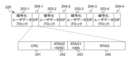
DIF202はT10-DIFの規格に従っており、2バイトのCRC(Cyclic Redundancy Check)231、2バイトのATAG(Application Tag)(0)232、2バイトのATAG(1)233、4バイトのRTAG(Reference Tag)234から構成される。 The DIF 202 conforms to the T10-DIF standard and is composed of a 2-byte CRC (Cyclic Redundancy Check) 231, a 2-byte ATAG (Application Tag) (0) 232, a 2-byte ATAG (1) 233, and a 4-byte RTAG (Reference Tag) 234.
CRC231は、DIF202の前に位置する512バイトのユーザデータブロック201から算出される16ビットの誤り検出符号である。RTAG234は、DIF202の前に位置する512バイトのユーザデータブロック201に対応づけられたアドレスである。RTAG234に設定するアドレスは、ユーザデータの先頭のユーザデータブロック201から終端のユーザデータブロック201に向かって昇順に設定される。例えば、ユーザデータブロック201-1のアドレスがK(Kは整数)である場合、ユーザデータブロック201-2のアドレスはK+1、ユーザデータブロック201-3のアドレスはK+2、ユーザデータブロック201-4のアドレスはK+3である。ATAG(0)232及びATA(1)233は任意の用途に用いることができる。ユーザデータをDRAM134にキャッシュしている場合、ATAG(0)232及びATAG(1)233は使用されないため、ストレージシステム120はATAG(0)232及びATAG(1)233の各々に00hを設定する。
ストレージシステム120は、DRAM134に格納されるユーザデータの各ユーザデータブロック201にDIF202を付加することによって、ライト処理/リード処理におけるエラーの発生を検出できる。具体的には、ストレージシステム120は、CRC231を検査することによって、ユーザデータブロック201の破損を検出できる。ストレージシステム120は、RTAG234を検査することによって、ユーザデータブロック201の順序が入れ替わりを検出できる。FE I/F131がホスト計算機110にユーザデータを送信する場合に行うDIF検査は、前述の検査である。
The
図2Cに示すデータフォーマット220は、ストレージシステム120がストレージデバイス140に保存する暗号化ユーザデータのフォーマットの一例である。図2Cに示す暗号化ユーザデータは、ユーザデータブロック201-1、201-2、201-3、201-4を暗号化した暗号化ユーザデータブロック203-1、203-2、203-3、203-4から構成される。
The
ストレージシステム120は、ユーザデータを構成する各ユーザデータブロック201をAES(Advanced Encryption Standard)アルゴリズムのXTS(XEX encryption mode with Tweak and ciphertext Stealing)モードを用いて、暗号化ユーザデータブロック203に暗号化する。
The
AESは、米国国立標準技術研究所(NIST)が標準暗号として定めた共通鍵暗号アルゴリズムである。AES鍵のサイズは、例えば256ビットである。ただし、ASE鍵のサイズは256ビットでなくてもよい。XTSモードは、標準化文章IEEE1619で制定されているストレージデバイス向けのブロック暗号方式である。以下の説明では、AESアルゴリズムのXTSモードによる暗号化をXTS暗号化、当該モードによる復号をXTS復号と記載する。 AES is a symmetric key encryption algorithm defined as a standard encryption by the National Institute of Standards and Technology (NIST). The size of the AES key is, for example, 256 bits. However, the size of the ASE key does not have to be 256 bits. The XTS mode is a block encryption method for storage devices established in the standard document IEEE 1619. In the following explanation, encryption using the XTS mode of the AES algorithm will be referred to as XTS encryption, and decryption using this mode will be referred to as XTS decryption.
ストレージシステム120は、ユーザデータのキャッシュと同様に、各暗号化ユーザデータブロック203にDIF204を付加する。
The
DIF204は、DIF202と同様にT10-DIFの規格に従っており、2バイトのCRC241、2バイトのATAG(0)242、2バイトのATAG(1)243、4バイトのRTAG244から構成される。 DIF204, like DIF202, conforms to the T10-DIF standard and is composed of a 2-byte CRC241, a 2-byte ATAG(0)242, a 2-byte ATAG(1)243, and a 4-byte RTAG244.
CRC241は、DIF204の前に位置する512バイトの暗号化ユーザデータブロック203から算出される16ビットの誤り検出符号である。RTAG244は、DIF204の前に位置する512バイトの暗号化ユーザデータブロック203に対応づけられたアドレスである。RTAG244に設定するアドレスは、暗号化ユーザデータの先頭の暗号化ユーザデータブロック203から終端の暗号化ユーザデータブロック203に向かって昇順に設定される。ストレージシステム120は、暗号化ユーザデータをストレージデバイス140に保存する場合、ATAG(0)242にWSC(ライトシーケンスコード)と呼ばれる符号を設定する。WSCの仕様については図3を用いて説明する。ATAG(1)243は使用しないため、00hが設定される。
ストレージシステム120は、ストレージデバイス140に保存される暗号化ユーザデータの各暗号化ユーザデータブロック203にDIF204を付加することによって、書き込みエラー又は読み出しエラーの発生を検出できる。具体的には、ストレージシステム120は、CRC241を検査することによって、読み出した暗号化ユーザデータブロック203の破損を検出できる。ストレージシステム120は、RTAG244を検査することによって、ストレージデバイス140に読み出しを指示したアドレスの誤りを検出できる。ストレージデバイス140への暗号化ユーザデータの書き込みのエラーは、ATAG(0)242に設定されたWSCを検査することによって検出できる。
The
以下の説明では、ユーザデータブロック201及び暗号化ユーザデータブロック203を区別しない場合、データブロックと記載する。 In the following description, when there is no need to distinguish between user data block 201 and encrypted user data block 203, they will be referred to as data blocks.
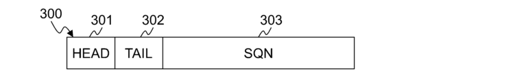
図3A、図3B、及び図3Cは、実施例1のWSCの仕様を説明する図である。 Figures 3A, 3B, and 3C are diagrams explaining the specifications of the WSC in Example 1.
図3Aに示すデータフォーマット300は、WSCのデータフォーマットの一例である。WSCは、ATAG0(242)に格納される1バイト(8ビット)の符号であり、1ビットのHEADフラグ301、1ビットのTAILフラグ302、6ビットのSQN(シーケンス番号)303から構成される。
The
HEADフラグ301は、ストレージデバイス140に書き込む暗号化ユーザデータブロック203が先頭であるか否かを示す値を格納するフラグである。TAILフラグ302は、ストレージデバイス140に書き込む暗号化ユーザデータブロック203が終端であるか否かを示す値を格納するフラグである。
The
ストレージデバイス140に書き込む暗号化ユーザデータブロック203が先頭である場合、HEADフラグ301に1が設定され、ストレージデバイス140に書き込む暗号化ユーザデータブロック203が終端である場合、TAILフラグ302に1が設定される。先頭及び終端のいずれにも該当しない暗号化ユーザデータブロック203のHEADフラグ301及びTAILフラグ302には0が設定される。1つの暗号化ユーザデータブロック203から構成される暗号化ユーザデータを書き込む場合、HEADフラグ301及びTAILフラグ302には1が設定される。
If the encrypted user data block 203 to be written to the storage device 140 is the first, the
SQN303はストレージデバイス140に書き込まれる暗号化ユーザデータの世代番号を格納する。世代番号は、書き込むたびに異なる値を用いる。 SQN303 stores the generation number of the encrypted user data written to the storage device 140. A different value is used for the generation number each time it is written.
図3Bは、ストレージデバイス140のアドレス0~9に暗号化ユーザデータブロック203を書き込む場合のWSCの設定例を示す。
Figure 3B shows an example of WSC settings when writing encrypted user data blocks 203 to
状態1では、10個の暗号化ユーザデータブロック203から構成される暗号化ユーザデータが書き込まれる。ここではSQNとして0x0Aが指定されているものとする。
In
アドレス0に書き込まれた暗号化ユーザデータブロック203は先頭であるためHEAD301は1となり、WSCは0x8Aとなる。アドレス9に書き込まれた暗号化ユーザデータブロック203は終端であるためTAIL302が1となり、WSCは0x4Aとなる。他のアドレスに書き込まれた暗号化ユーザデータブロック203のWSCは0x0Aとなる。
The encrypted user data block 203 written to address 0 is the first, so
状態2では、アドレス3~7に対して5つの暗号化ユーザデータブロック203から構成される暗号化ユーザデータが書き込まれる。ここではSQNには0x0Bが指定されているものとする。
In
5つのアドレスに対してデータが上書きされるためWSCが更新される。アドレス3に書き込まれた暗号化ユーザデータブロック203は先頭であるためHEAD301は1となり、WSCは0x8Bとなる。アドレス7に書き込まれた暗号化ユーザデータブロック230は終端であるためTAIL302は1となり、WSCは0x4Bとなる。アドレス4~6に書き込まれた暗号化ユーザデータブロック203のWSCは0x0Bとなる。
The WSC is updated because data is overwritten at five addresses. The encrypted user data block 203 written to address 3 is the first, so
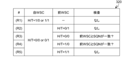
図3Cに示す表320は、WSCに基づいて書き込みエラーの有無を検査するためのルールの一例を示す。ストレージシステム120は、ストレージデバイス140に暗号化ユーザデータを書き込む場合、WSCを読み出して、表320に示したルールに従って、書き込みエラーの有無を検査する。
Table 320 in FIG. 3C shows an example of rules for checking for write errors based on the WSC. When the
表320には、以下のようなルールが定義されている。
(R1)自ブロックのWSCのHEAD/TAILが1/0又は1/1の場合、検査は行われない。
(R2)自ブロックのWSCのHEAD/TAILが0/0又は0/1、かつ、前のブロックのWSCのHEAD/TAILが0/1である場合、検査は行われない。
(R3)自ブロックのWSCのHEAD/TAILが0/0又は0/1、かつ、前のブロックのWSCのHEAD/TAILが0/0の場合、ストレージシステム120は、自ブロックのWSCのSQNが前ブロックのWSCのSQNと一致するか否かを検査する。
(R4)自ブロックのWSCのHEAD/TAILが0/0又は0/1、かつ、その前のブロックのWSCのHEAD/TAILが1/0の場合、ストレージシステム120は、自ブロックのWSCのSQNが前ブロックのWSCのSQNと一致するか否かを検査する。
(R5)自ブロックのWSCのHEAD/TAILが0/0又は0/1、かつ、前のブロックのWSCのHEAD/TAILが1/1の場合、検査は行われない。
In table 320, the following rules are defined:
(R1) If the HEAD/TAIL of the WSC of the own block is 1/0 or 1/1, no check is performed.
(R2) If the HEAD/TAIL of the WSC of the own block is 0/0 or 0/1 and the HEAD/TAIL of the WSC of the previous block is 0/1, no check is performed.
(R3) If the HEAD/TAIL of the WSC of the current block is 0/0 or 0/1 and the HEAD/TAIL of the WSC of the previous block is 0/0, the
(R4) If the HEAD/TAIL of the WSC of the own block is 0/0 or 0/1 and the HEAD/TAIL of the WSC of the previous block is 1/0, the
(R5) If the HEAD/TAIL of the WSC of the own block is 0/0 or 0/1 and the HEAD/TAIL of the WSC of the previous block is 1/1, no check is performed.
(R3)、(R4)は、自ブロックが先頭でなく、前ブロックが終端でなかった場合、暗号化ユーザデータブロック203のSQNの一致を検査することを表す。これによって、複数ブロックで構成されたユーザデータの書き込みが間欠なく成功しているか否かが確認できる。例えば、図3Bの矩形311、312、313に含まれるアドレスのWSCは(R3)、(R4)の条件に合致するため検査対象となる。アドレス3~7に対する5つのブロックの書き込みにおいて、アドレス5への書き込みが失敗していた場合、アドレス5のWSCは更新されず0x0Aのままとなる。このエラーはアドレス5のWSC検査において、アドレス5のSQN(0x0A)がアドレス4のSQN(0x0B)と不一致となることで検出可能である。アドレス3~7に対する5つのブロックの書き込みにおいて、アドレス3への書き込みが失敗していた場合、アドレス3のWSCは更新されず0x0Aのままとなる。このエラーはアドレス4のWSC検査において、SQN(0x0B)がアドレス3のSQN(0x0A)と不一致となることで検出可能である。
(R3) and (R4) indicate that if the current block is not the first block and the previous block is not the last block, the SQN of the encrypted user data block 203 is checked for consistency. This allows you to check whether the writing of user data consisting of multiple blocks is successful without interruption. For example, the WSC of the addresses included in the
(R1)、(R2)、(R5)は、自ブロックが先頭である場合、又は、前のブロックが終端である場合、自ブロックのWSCのSQNと、前のブロックのWSCのSQNとが一致している必要がないため、検査を行わないことを表す。 (R1), (R2), and (R5) indicate that if the current block is the first block or the previous block is the last block, the SQN of the WSC of the current block does not need to match the SQN of the WSC of the previous block, so no check is performed.
図4は、実施例1のストレージシステム120が実行するライト処理の一例を説明するフローチャートである。以下の説明では、XTS暗号化されていないユーザデータブロック201を平文ブロック、XTS暗号化によって暗号化ユーザデータブロック203を暗号文ブロックと記載する。
Figure 4 is a flowchart illustrating an example of a write process executed by the
ストレージシステム120は、ホスト計算機110からライトコマンドとともにユーザデータを受信する(ステップS401)。
The
ストレージシステム120は、ユーザデータを構成する平文ブロックにDIF202を付加する(ステップS402)。具体的には、FE I/F131は、平文ブロックから16ビットの誤り検出符号を算出してCRC231として設定し、また、ブロックアドレスをTRAG234として設定する。
The
ストレージシステム120のCPU133は、DIF202を付加したユーザデータをDRAM134に格納する(ステップS403)。このとき、ストレージシステム120は、ユーザデータの損失を防ぐために、ユーザデータを多重してDRAM134に格納する。
The
ストレージシステム120のCPU133は、DRAM134から平文ブロックの一部を読み出し、レジスタにロードする(ステップS404)。
The
ストレージシステム120のCPU133は、レジスタにロードされたデータを用いて平文ブロックのCRCを算出するための演算(CRC計算)を実行し、XTS暗号化によってデータを暗号化する(ステップS405)。これによって、暗号文ブロックの一部が生成される。暗号化されたデータはレジスタに格納され、また、DRAM134にも格納される。
The
ストレージシステム120のCPU133は、レジスタに格納される暗号化されたデータを用いて、暗号文ブロックのCRCを算出するためのCRC計算を実行する(ステップS406)。
The
ストレージシステム120のCPU133は、全ての平文ブロックの暗号化が完了したか否かを判定する(ステップS407)。
The
全ての平文ブロックの暗号化が完了していない場合、ストレージシステム120のCPU133は、ステップS404に戻り同様の処理を実行する。このように、ストレージシステム120は、平文ブロックの先頭から終端に向かってロード元ポイントを順次移動させ、逐次的にデータを暗号化する。
If encryption of all plaintext blocks has not been completed, the
全ての平文ブロックの暗号化が完了した場合、平文ブロック及び暗号文ブロックのそれぞれのCRCが算出され、また、暗号化ユーザデータが生成された状態となっている。 When encryption of all plaintext blocks is complete, the CRCs of the plaintext blocks and ciphertext blocks are calculated, and encrypted user data is generated.
ストレージシステム120のCPU133は、算出された平文ブロックのCRCと、DIF202に含まれるCRC231とを比較することによって、ユーザデータが破損しているか否かを判定する(ステップS408)。具体的には、各CRCが一致しているか否かが判定される。少なくとも一つのCRCが不一致の場合、ユーザデータが破損していると判定される。
The
CRCの検査によってユーザデータの破損が検出された場合、ストレージシステム120のCPU133は、多重化されたユーザデータを用いてユーザデータを回復し(ステップS410)、その後、ステップS404に戻る。
If the CRC check detects corruption of the user data, the
CRCの検査によってユーザデータの破損が検出されなかった場合、ストレージシステム120のCPU133は、DIF202に含まれるRTAG234に基づいて、ユーザデータが破損しているか否かを判定する(ステップS409)。具体的には、アドレスが昇順になっているか否かが判定される。アドレスが昇順になっていない場合、ユーザデータが破損していると判定される。
If the CRC check does not detect any corruption of the user data, the
RTAG234の検査によってユーザデータの破損が検出された場合、ストレージシステム120のCPU133は、多重化されたユーザデータを用いてユーザデータを回復し(ステップS410)、その後、ステップS404に戻る。
If corruption of user data is detected by inspection of RTAG234, the
RTAG234の検査によってユーザデータの破損が検出されなかった場合、ストレージシステム120のCPU133は、各暗号文ブロックにDIF204を付加する(ステップS411)。具体的には、暗号文ブロックから算出された16ビットの誤り検出符号がCRC241に設定され、図3で説明したWSCがATAG0(242)に設定され、暗号文ブロックのアドレスがRTAG234に設定される。
If no corruption of user data is detected by checking the
ストレージシステム120のCPU133は、DIF204が付加された暗号化ユーザデータをストレージデバイス140にライトする(ステップS412)。この時、CPU133は、N-1等分に分割された暗号化ユーザデータと、RAID技術によって生成されたパリティとを複数のストレージデバイス140にライトする。以上がライト処理の説明である。
The
図5は、実施例1のストレージシステム120が実行するリード処理の一例を説明するフローチャートである。
Figure 5 is a flowchart illustrating an example of a read process executed by the
ストレージシステム120のCPU133は、ホスト計算機110からリードコマンドを受信した場合、ストレージデバイス140からDIF204が付加された暗号化ユーザデータを読み出し、DRAM134に格納する(ステップS501)。
When the
ストレージシステム120のCPU133は、DRAM134から暗号文ブロックの一部をレジスタにロードする(ステップS502)。
The
ストレージシステム120のCPU133は、レジスタにロードされたデータを用いて暗号文ブロックのCRCを算出するための演算(CRC計算)を実行し、XTS復号によってデータを復号する(ステップS503)。これによって、平文ブロックの一部が生成される。復号されたデータはレジスタに格納され、また、DRAM134にも格納される。
The
ストレージシステム120のCPU133は、レジスタに格納される復号されたデータを用いて、平文ブロックのCRCを算出するための演算(CRC計算)を実行する(ステップS504)。
The
ストレージシステム120のCPU133は、全ての暗号文ブロックの復号が完了したか否かを判定する(ステップS505)。
The
全ての暗号文ブロックの復号が完了していない場合、ストレージシステム120のCPU133は、ステップS502に戻り同様の処理を実行する。このように、暗号文ブロックの先頭から終端に向かってロード元ポイントを順次移動させ、逐次的にデータを復号する。
If decryption of all ciphertext blocks has not been completed, the
全ての暗号文ブロックの復号が完了した場合、暗号文ブロック及び平文ブロックのそれぞれのCRCが算出され、また、ユーザデータが生成された状態となっている。 When all ciphertext blocks have been decrypted, the CRCs of the ciphertext blocks and plaintext blocks have been calculated, and user data has been generated.
ストレージシステム120のCPU133は、算出された暗号文ブロックのCRCと、DIF204に含まれるCRC241とを比較することによって、暗号化ユーザデータが破損しているか否かを判定する(ステップS506)。すなわち、暗号化ユーザデータのリード又はライトに失敗しているか否かが判定される。具体的には、各CRCが一致しているか否かが判定される。少なくとも1つのCRCが不一致である場合、暗号化ユーザデータが破損していると判定される。
The
CRCの検査によって暗号化ユーザデータの破損が検出された場合、ストレージシステム120のCPU133は、ストレージシステム120からパリティを読み出し、暗号化ユーザデータを回復し(ステップS509)、その後、ステップS502に戻る。
If the CRC check detects corruption of the encrypted user data, the
CRCの検査によって暗号化ユーザデータの破損が検出されなかった場合、ストレージシステム120のCPU133は、DIF204に含まれるWSCに基づいて、暗号化ユーザデータが破損しているか否かを判定する(ステップS507)。すなわち、暗号化ユーザデータのリード又はライトに失敗しているか否かが判定される。具体的には、図3Cに示した表320に従った検査が行われる。
If the CRC check does not detect any corruption of the encrypted user data, the
WSCの検査によって暗号化ユーザデータの破損が検出された場合、ストレージシステム120のCPU133は、ストレージシステム120からパリティを読み出し、暗号化ユーザデータを回復し(ステップS509)、その後、ステップS502に戻る。
If corruption of the encrypted user data is detected by the WSC inspection, the
WSCの検査によって暗号化ユーザデータの破損が検出されなかった場合、ストレージシステム120のCPU133は、DIF204に含まれるRTAG234に基づいて、暗号化ユーザデータが破損しているか否かを判定する(ステップS508)。すなわち、暗号化ユーザデータのリード又はライトに失敗しているか否かが判定される。具体的には、アドレスが昇順になっているか否かが判定される。アドレスが昇順になっていない場合、暗号化ユーザデータが破損していると判定される。
If the WSC inspection does not detect corruption of the encrypted user data, the
RTAG234の検査によって暗号化ユーザデータの破損が検出された場合、ストレージシステム120のCPU133は、ストレージシステム120からパリティを読み出し、暗号化ユーザデータを回復し(ステップS509)、その後、ステップS502に戻る。
If corruption of the encrypted user data is detected by inspection of RTAG234, the
RTAG234の検査によってユーザデータの破損が検出されなかった場合、ストレージシステム120のCPU133は、各平文ブロックにDIF202を付加する(ステップS510)。具体的には、平文ブロックから算出された16ビットの誤り検出符号がCRC231に設定され、平文ブロックのアドレスがRTAG234に設定される。
If no corruption of user data is detected by checking the
ストレージシステム120のCPU133は、DIF202が付加されたユーザデータをDRAM134に格納する(ステップS511)。
The
ストレージシステム120は、ホスト計算機110にユーザデータを送信する(ステップS512)。この時、FE I/F131は、DIFの検査を行って、ユーザデータからDIFを除去する。以上がリード処理である。
The
図6A及び図6Bは、従来のXTS暗号化/復号を説明する図である。 Figures 6A and 6B are diagrams explaining conventional XTS encryption/decryption.
図6Aは、XTS暗号化の処理手順を示す。XTS暗号化では、512バイトの平文ブロックが16バイトずつ暗号化される。まず、(E1)16バイトのTweakと平文ブロックの一部との排他的論理和が算出される。次に、(E2)AES暗号化アルゴリズムに基づく暗号化が行われる。最後に、(E3)暗号化の結果とTweakとの排他的論理和が算出され、16バイトの暗号文要素が生成される。(E1)、(E2)、(E3)の処理のサイクルを32回実行することによって512バイトの暗号文ブロックが生成される。 Figure 6A shows the procedure for XTS encryption. In XTS encryption, a 512-byte plaintext block is encrypted in 16-byte chunks. First, (E1) an exclusive-OR is calculated between a 16-byte tweak and a part of the plaintext block. Next, (E2) encryption is performed based on the AES encryption algorithm. Finally, (E3) an exclusive-OR is calculated between the encryption result and the tweak to generate a 16-byte ciphertext element. A 512-byte ciphertext block is generated by performing the process cycle of (E1), (E2), and (E3) 32 times.
Tweakは16バイトのデータを暗号化する毎に変更される。また、Tweakは512バイトのブロック毎に異なる値である。
Tweak is changed every
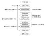
(E2)のAESアルゴリズムでは15個の暗号化ラウンド鍵(128ビット)を用いて暗号化が行われる。これらのラウンド鍵は、規定された拡張処理(Key Expansion)を256ビット暗号鍵に施して生成される。最初に、(E2-1)AddRoundKey処理が実行され、次に、(E2-2)SubBytes、ShiftRows、MixColumns、AddRoundKeyの4つの処理が13回繰り返され、最後に、(E2-3)SubBytes、ShiftRows、AddRoundKeyの3つの処理が実行される。15回実行されるAddRoundKey処理では、暗号化ラウンド鍵0~14が使用される。
In the AES algorithm (E2), encryption is performed using 15 encryption round keys (128 bits). These round keys are generated by applying a prescribed expansion process (Key Expansion) to a 256-bit encryption key. First, (E2-1) AddRoundKey process is performed, then (E2-2) four processes of SubBytes, ShiftRows, MixColumns, and AddRoundKey are repeated 13 times, and finally (E2-3) three processes of SubBytes, ShiftRows, and AddRoundKey are performed. In the AddRoundKey process, which is performed 15 times,
前述した各処理は、以下のようなCPU命令に対応させることができる。データ及びTweakの排他的論理和はXOR命令に対応する。AddRoundKey処理は、CPU命令として、前段の処理結果と暗号化ラウンド鍵との排他的論理和(XOR)に対応する。(E2-2)の4つの処理は、AESENC命令に対応する。つまり、AESENC命令は13回実行する必要がある。(E2-3)の3つの処理は、AESENCLAST命令に対応する。AESENC命令とAESENCLAST命令は、Intel社が2010年頃以降に製品化しているマイクロプロセッサにおいて、AES-NI(AES New Instructions)と呼ばれる暗号専用命令セットの一部として実装されている。 Each of the above processes can be associated with the following CPU instructions. The exclusive OR of data and Tweak corresponds to the XOR instruction. The AddRoundKey process corresponds to the exclusive OR (XOR) of the previous process result and the encryption round key as a CPU instruction. The four processes in (E2-2) correspond to the AESENC instruction. In other words, the AESENC instruction needs to be executed 13 times. The three processes in (E2-3) correspond to the AESENCLAST instruction. The AESENC and AESENCLAST instructions are implemented as part of a dedicated encryption instruction set called AES-NI (AES New Instructions) in microprocessors that Intel has commercialized since around 2010.
図6Bは、XTS復号の処理手順を示す。XTS復号では、512バイトの暗号文ブロックが16バイトずつ復号される。まず、(D1)16バイトのTweakと暗号化ブロックの一部との排他的論理和が算出される。次に、(D2)AESアルゴリズムに基づく復号が行われる。最後に、(D3)復号の結果とTweakとの排他的論理和が算出され、16バイトの平文要素が生成される。(D1)、(D2)、(D3)を32回実行することによって512バイトの平文ブロックが生成される。 Figure 6B shows the procedure for XTS decryption. In XTS decryption, a 512-byte ciphertext block is decrypted in 16-byte chunks. First, (D1) an exclusive-OR is calculated between a 16-byte tweak and a part of the encrypted block. Next, (D2) decryption is performed based on the AES algorithm. Finally, (D3) an exclusive-OR is calculated between the decryption result and the tweak to generate a 16-byte plaintext element. A 512-byte plaintext block is generated by executing (D1), (D2), and (D3) 32 times.
Tweakは16バイトのデータを復号する毎に変更される。また、Tweakは512バイトのブロック毎に異なる値である。
Tweak is changed every
(D2)のAES復号アルゴリズムでは15個の復号ラウンド鍵(128ビット)を用いて復号が行われる。これらのラウンド鍵は、規定された拡張処理(Key Expansion)を256ビット暗号鍵に施して生成する。256ビット暗号鍵は暗号化で使用した暗号鍵と同一である。最初に、(D2-1)AddRoundKey処理が実行され、次に、(D2-2)InvShiftRows、InvSubBytes、AddRoundKey、InvMixColumnsの4つの処理が13回繰り返され、最後に、(D2-3)InvShiftRows、InvSubBytes、AddRoundKeyの3つの処理が実行される。15回実行されるAddRoundKey処理では、復号ラウンド鍵0~14が使用される。
In the AES decryption algorithm (D2), decryption is performed using 15 decryption round keys (128 bits). These round keys are generated by applying a prescribed expansion process (Key Expansion) to a 256-bit encryption key. The 256-bit encryption key is the same as the encryption key used in encryption. First, (D2-1) AddRoundKey processing is performed, then (D2-2) four processes of InvShiftRows, InvSubBytes, AddRoundKey, and InvMixColumns are repeated 13 times, and finally (D2-3) three processes of InvShiftRows, InvSubBytes, and AddRoundKey are performed. In the AddRoundKey processing, which is performed 15 times,
前述した各処理は、以下のようなCPU命令に対応させることができる。データ及びTweakの排他的論理和はXOR命令に対応する。AddRoundKey処理は、前段の処理結果と復号ラウンド鍵との排他的論理和(XOR)に対応する。(D2-2)の4つの処理は、AESDEC命令に対応する。つまり、AESDEC命令は13回実行する必要がある。(D2-3)の3つの処理は、AESDECLAST命令に対応する。AESDEC命令とAESDECLAST命令は、上記と同様にAES-NIの一部として実装されている。 Each of the above processes can be associated with a CPU instruction as follows. The exclusive OR of data and Tweak corresponds to the XOR instruction. The AddRoundKey process corresponds to the exclusive OR (XOR) of the previous process result and the decryption round key. The four processes in (D2-2) correspond to the AESDEC instruction. In other words, the AESDEC instruction needs to be executed 13 times. The three processes in (D2-3) correspond to the AESDECLAST instruction. The AESDEC and AESDECLAST instructions are implemented as part of AES-NI, as above.
図7A、図7B、及び図7Cは、実施例1のストレージシステム120におけるXTS暗号化/復号を説明する図である。
Figures 7A, 7B, and 7C are diagrams explaining XTS encryption/decryption in the
CPU133は、第3世代Xeonスケーラブルプロセッサ等であり、AES-NIをサポートし、さらにその中のAESENC命令、AESENCLAST命令、AESDEC命令、AESDECLAST命令のそれぞれをVector化した命令(VAESENC命令、VAESENCLAST命令、VAESDEC命令、VAESDECLAST命令)もサポートしている。
The
Vecror命令は、1回の実行において、複数データに対して同じ演算を並列に実施することができる命令である。SIMD(Single Instruction/Multiple Data)命令とも呼ばれる。Vector命令ではZmmレジスタと呼ばれる512ビット(64バイト)レジスタを使用し、128ビット(16バイト)の4つのデータに対して同じ演算を実行する。演算結果もまたZmmレジスタに格納される。CPU133は、32個のZmmレジスタ(Zmm0レジスタ~Zmm31レジスタ)を利用する。CPU133は、マイクロプロセッサに一般的な演算(加算、減算、乗算、排他的論理和、シフト、比較など)を行う命令についても、Vector化した命令をサポートしている。
A Vector instruction is an instruction that can perform the same operation on multiple pieces of data in parallel in one execution. It is also called a SIMD (Single Instruction/Multiple Data) instruction. A Vector instruction uses a 512-bit (64-byte) register called a Zmm register to perform the same operation on four pieces of 128-bit (16-byte) data. The operation result is also stored in the Zmm register. The
CPU133は、これらのVector命令を用いてXTS暗号化/復号を並列的に実行する。具体的には、4つのデータブロック(512バイト)を並列で暗号化/復号する。
The
図7Aは、CPU133による、4つの平文ブロックの並列的なXTS暗号化を示す。
Figure 7A shows parallel XTS encryption of four plaintext blocks by
CPU133は、DRAM134に格納された4つの平文ブロック(512バイト)の各々から16バイトのデータをZmmレジスタにロードする。Zmmレジスタには合計で64バイトのデータが格納される。
The
CPU133は、(P1)Vector XOR命令を実行することによって、Zmmレジスタに格納されるデータと、各平文ブロックの4つのTweakを並べた値との排他的論理和を算出する。次に、CPU133は、(P2)Vector XOR命令、13回のVAESENC命令、及びVAESENCLAST命令を実行することによって、4つの平文ブロックのXTS暗号化を並列で行う。最後に、CPU133は、(P3)(P2)の演算結果と、4つのTweakを並べた値との排他的論理和を算出する。これによって、4つの16バイトの暗号文要素が同時に生成される。
The
暗号文要素はZmmレジスタから逐次DRAM134に格納される。(P1)、(P2)、(P3)の処理のサイクルを複数回実行することによって、4つの暗号文ブロック(512バイト)が生成される。なお、(P2)で用いる暗号化ラウンド鍵0~14は各平文ブロックで共通である。
The ciphertext elements are stored sequentially from the Zmm register to the
図7Bは、CPU133による、4つの暗号文ブロックの並列的なXTS復号を示す。
Figure 7B shows parallel XTS decryption of four ciphertext blocks by
CPU133は、DRAM134に格納された4つの暗号文ブロック(512バイト)の各々から16バイトのデータをZmmレジスタにロードする。Zmmレジスタには合計で64バイトのデータが格納される。
The
CPU133は、(P4)Vector XOR命令を実行することによって、Zmmレジスタに格納されるデータと、各暗号文ブロックの4つのTweakを並べた値との排他的論理和を算出する。次に、CPU133は、(P5)Vector XOR命令、13回のVAESDEC命令、及びVAESDECLAST命令を実行することによって、4つの暗号文ブロックのXTS復号を並列で行う。最後に、CPU133は、(P6)(P5)の演算結果と、4つのTweakを並べた値との排他的論理和を算出する。これによって、4つの16バイトの平文要素が同時に生成される。
The
平文要素はZmmレジスタから逐次DRAM134に格納される。(P4)、(P5)、(P6)の処理のサイクルを複数回実行することによって、4つの平文ブロック(512バイト)が生成される。なお、(P5)で用いる復号ラウンド鍵0~14は各暗号文ブロックで共通である。
The plaintext elements are stored sequentially from the Zmm register to the
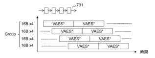
図7Cは、Vector化した上記4種のAES命令の実行順序を最適化する方法を示す。 Figure 7C shows how to optimize the execution order of the above four vectorized AES instructions.
図7CのVAES*は、VAESENC、VAESENCLAST、VAESDEC、VAESDECLASTに置き換えられる。 VAES* in Figure 7C is replaced with VAESENC, VAESENCLAST, VAESDEC, and VAESDECLAST.
これらの命令で用いる演算回路はそれぞれ4段のパイプライン構造731となっており、処理完了までのサイクル数は4である。パイプライン回路は、データがN段目から(N+1)段目に移行した時に、N段目は次のデータを受け入れ可能である。そのため、VAES*命令を4つ並べて実行すると、パイプラインには4サイクル連続でデータを供給できるため、処理効率が向上する。この考え方に基づき、CPU133は、図7Aに示す暗号化及び図7Bに示す復号において、4つのデータブロックからそれぞれ16バイトをZmmレジスタにロードする場合に、4つのZmmレジスタを確保して16バイト×4のロードを4回分先行して行う。そして、CPU133は、4つのZmmレジスタに対する4つのVAES*命令を連続で実行し、パイプライン処理の効率を向上させる。以下、4連続のVAES*命令で処理されるデータのまとまりをGroupと呼ぶ。
The arithmetic circuits used in these instructions each have a four-
図8は、実施例1のストレージシステム120が実行するVector命令を用いたXTS暗号化/復号における入力データの構造を示す図である。
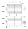
Figure 8 is a diagram showing the structure of input data for XTS encryption/decryption using the Vector command executed by the
4つのデータブロックのXTS暗号化/復号の並列実行においては、図7Cで示すGourpはGourp0~7の8個から構成される。すなわち、「4つのZmmレジスタに対して4つのVAES*命令を連続で実行する」手順は、4つのデータブロックのXTS暗号化/復号の並列処理の1回の実行において8回実行される。
In parallel execution of XTS encryption/decryption of four data blocks, the Group shown in FIG. 7C is made up of eight Groups,
1つのGroupを構成する4つの64バイトデータ(16バイト×4)はそれぞれZmm0レジスタ~Zmm3レジスタにロードされる。例えば、Zmm0レジスタにロードされるデータは破線810で囲った64バイトデータである。なお、ロード先のZmmレジスタの番号は一例であって、他のレジスタ番号でもよい。
The four 64-byte data (16 bytes x 4) that make up one Group are loaded into the Zmm0 to Zmm3 registers, respectively. For example, the data loaded into the Zmm0 register is the 64-byte data enclosed by the dashed
DRAM134に格納されるユーザデータ又は暗号化ユーザデータの各データブロックの終端にはそれぞれ8バイトのDIFが付加されている。4つのデータブロックのDIFの検査は並列で実行されるため、1つのZmmレジスタにDIFがロードされる。図8では、Zmm8レジスタに4つのデータブロックに付加されたDIFがロードされている。
An 8-byte DIF is added to the end of each data block of user data or encrypted user data stored in
Zmmレジスタは16バイトのデータを4つ保持可能である。ただし、DIFは8バイトであるため、8バイトの間隔をあけてZmmレジスタにロードされる。なお、DIFロード先のZmmレジスタの番号は一例であって、他のレジスタ番号でもよい。 The Zmm register can hold four 16-byte data items. However, since DIF is 8 bytes, it is loaded into the Zmm register with 8-byte intervals between each. Note that the number of the Zmm register into which DIF is loaded is just an example, and other register numbers may be used.
XTS暗号化/復号処理に同時に入力される4つのデータブロックのアドレスは昇順で連続しており、4N、4N+1、4N+2、4N+3(Nは整数)である。例えば、ライト/リードするユーザデータのサイズが128Kバイト(256ブロック)の場合、4つのデータブロックのXTS暗号化/復号の並列処理を64回行う必要がある。 The addresses of the four data blocks input simultaneously to the XTS encryption/decryption process are consecutive in ascending order: 4N, 4N+1, 4N+2, 4N+3 (N is an integer). For example, if the size of the user data to be written/read is 128 KB (256 blocks), the XTS encryption/decryption of the four data blocks must be performed in parallel 64 times.
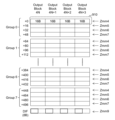
図9は、実施例1のストレージシステム120が実行するVector命令を用いたXTS暗号化/復号における出力データの構造を示す図である。
Figure 9 is a diagram showing the structure of output data in XTS encryption/decryption using the Vector command executed by the
図9のGourp0~7は、図8のGourp0~7のデータをXTS暗号化/復号した結果をDRAM134に格納する場合の出力位置に対応する。XTS暗号化/復号の結果の出力先の位置関係は入力元のそれと同じである。すなわち、入力ブロック先頭位置がX、出力ブロック先頭位置がYの時、入力ブロック先頭からP(Pは0以上)だけ離れたX+Pの位置にあるデータをXTS暗号化/復号した結果はY+Pの位置に出力される。
1つのGroupをXTS暗号化/復号した結果はZmm4~7の4つのレジスタに保持されており、4つの64バイトのデータ(16バイト×4)はこの規則に従った位置に格納される。例えば、破線910で囲った64バイトのデータは、図8の破線810で囲った64バイトのデータのXTS暗号化/復号の結果であり、Zmm4レジスタに格納される。なお、これら格納元のZmmレジスタの番号は一例であって、他のレジスタ番号でもよい。
The results of XTS encryption/decryption of one Group are held in four registers, Zmm4 to 7, and the four 64-byte data (16 bytes x 4) are stored in positions that follow this rule. For example, the 64 bytes of data enclosed by dashed
DRAM134に格納されるユーザデータ又は暗号化ユーザデータの各データブロックの終端にはそれぞれ8バイトのDIFが格納される。4つのブロックのDIFの生成は並列で実行されため、1つのZmmレジスタからDIFが読み出される。図9では、Zmm9からDIFが読み出されている。
An 8-byte DIF is stored at the end of each data block of user data or encrypted user data stored in
Zmm9レジスタに格納されるDIFは8バイトの間隔をあけて格納される。なお、DIFの格納元のZmmレジスタの番号は一例であって、他のレジスタ番号でもよい。 The DIF stored in the Zmm9 register is stored with 8-byte intervals. Note that the number of the Zmm register from which the DIF is stored is just an example, and other register numbers may be used.
XTS暗号化/復号処理の結果が同時に出力される4つのデータブロックのアドレスは、図8と同様に昇順で連続しており、4N、4N+1、4N+2、4N+3(Nは整数)である。 The addresses of the four data blocks to which the results of the XTS encryption/decryption process are output simultaneously are consecutive in ascending order, as in Figure 8, and are 4N, 4N+1, 4N+2, and 4N+3 (N is an integer).
以上、図7~9を用いて説明した、4つデータブロックのXTS暗号化/復号の並列処理は、図4のステップS405及び図5のステップS503において適用される。 The parallel processing of XTS encryption/decryption of four data blocks described above using Figures 7 to 9 is applied in step S405 of Figure 4 and step S503 of Figure 5.
図10A、図10B、及び図10Cは、実施例1のストレージシステム120におけるCRCの算出方法を説明する図である。
Figures 10A, 10B, and 10C are diagrams explaining the CRC calculation method in the
まず、図10Aを参照しながら、CRC計算の理論を説明する。一般に、バイナリ多項式M(x)に対応する任意長のバイナリデータMのCRCは式(1)で定義される。 First, the theory of CRC calculation will be explained with reference to FIG. 10A. In general, the CRC of binary data M of any length corresponding to a binary polynomial M(x) is defined by equation (1).
![]()
![]()
ここで、degは多項式の次数を表し、P(x)はCRCアルゴリズムを定義する多項式を表し、記号「・」はキャリーレス乗算を表す。16ビットCRCアルゴリズムの場合、P(x)は次数16の多項式である。CRCは、ガロア体GF(2)上で定義された大きな次数の多項式M(x)をCRC多項式P(x)で割った時の剰余多項式として計算できる。
Here, deg represents the degree of the polynomial, P(x) represents the polynomial that defines the CRC algorithm, and the symbol "." represents carry-less multiplication. For a 16-bit CRC algorithm, P(x) is a polynomial of
図10Aは、ストレージシステム120において典型的な512バイト(4096ビット)のブロックから16ビットのCRCを算出する方法を示している。キャリーレス乗算を効率的に実行できるCPU命令があれば、バイナリ多項式の除算は効率的に実行できる。
Figure 10A shows how a 16-bit CRC is calculated from a typical 512-byte (4096-bit) block in
図10B及び図10Cは、最大で64ビット×64ビットのキャリーレス乗算が実行可能なPCLMULQDQ命令を用いたCRC計算の方法を示している。PCLMULQDQ命令は、Intel社が2010年頃以降に製品化しているマイクロプロセッサに搭載されている。 Figures 10B and 10C show a method of CRC calculation using the PCLMULQDQ instruction, which can perform carry-less multiplication of up to 64 bits by 64 bits. The PCLMULQDQ instruction is included in microprocessors that Intel has commercialized since around 2010.
図10Bは、512バイト(4096ビット)のバイナリデータのCRC計算を、128ビットのバイナリデータのCRC計算に短縮する方法を示している。1回の短縮処理によってバイナリデータのビット数は128だけ減る。k回の短縮処理を施した後のバイナリ多項式Mk(x)と、さらに1回の短縮処理を施して得られる多項式Mk+1(x)との関係は式(2)で与えられる。 Figure 10B shows a method for shortening the CRC calculation of 512 bytes (4096 bits) of binary data to a CRC calculation of 128 bits of binary data. The number of bits of the binary data is reduced by 128 by one shortening process. The relationship between the binary polynomial Mk(x) after k shortening processes and the polynomial Mk+1(x) obtained by one further shortening process is given by equation (2).

ここで、M0(x)=M(x)である。H(x)はMk(x)が示すバイナリデータの上位64ビットからなる多項式を表し、L(x)はMk(x)が示すバイナリデータの上位64ビットに続く64ビットからなる多項式を表す。Gk(x)はMk(x)が示すバイナリデータの上位128ビットを除いた残りデータからなる多項式を表す。Tは当該残りデータのビット数を表す。記号「+」はビット単位の排他的論理和を表す。 Here, M0(x) = M(x). H(x) represents a polynomial consisting of the upper 64 bits of the binary data represented by Mk(x), and L(x) represents a polynomial consisting of the 64 bits following the upper 64 bits of the binary data represented by Mk(x). Gk(x) represents a polynomial consisting of the remaining data excluding the upper 128 bits of the binary data represented by Mk(x). T represents the number of bits of the remaining data. The symbol "+" represents a bitwise exclusive OR.
PCLMULQDQ命令によって、H(x)とL(x)が示す64ビット値にそれぞれ定数を乗じて2つの128ビット値を求め、それらとGk(x)が示す残りデータとの排他的論理和を算出することによって、CRC計算の対象となるバイナリデータのビット数を128だけ減らすことができる。この短縮処理を31回行うことで、512バイト(4096ビット)のバイナリデータのCRC計算は、M31(x)が示す128ビットのバイナリデータのCRC計算に帰着する。 The PCLMULQDQ instruction multiplies the 64-bit values indicated by H(x) and L(x) by a constant to obtain two 128-bit values, and then calculates the exclusive OR of these values with the remaining data indicated by Gk(x), thereby reducing the number of bits of binary data subject to CRC calculation by 128. By performing this shortening process 31 times, the CRC calculation of 512 bytes (4096 bits) of binary data is reduced to the CRC calculation of the 128-bit binary data indicated by M31(x).
図10Cは、M31(x)が示す128ビットのバイナリデータのCRC計算(図10Bの最終計算)を行う方法を示している。 Figure 10C shows how to perform the CRC calculation (the final calculation in Figure 10B) on the 128-bit binary data represented by M31(x).
まず、CPU133は、PCLMULQDQ命令によって、上位64ビット値に定数を乗じて80ビット値(1031)を求め、それと下位64ビット値との排他的論理和を算出することによって、CRC計算の対象データのビット数を80に減らす。次に、CPU133は、PCLMULQDQ命令によって、その上位32ビット値に定数を乗じて48ビット値(1032)を求め、それと80ビット値(1031)の下位48ビットとの排他的論理和を算出することによって、CRC計算の対象データのビット数を48に減らす。その結果をRとする。最後に、CPU133は、Barrett Reductionと呼ばれるアルゴリズムに基づいて、48ビットのRから16ビットのCRCを算出する。具体的には、CPU133が、式(3)、(4)、(5)、(6)を順で演算を行う。
First, the
![]()
![]()
![]()
![]()
![]()
![]()
![]()
![]()
ここで、R(x)はRからなる多項式を表し、Floorは多項式からxの0次以上の項を残す操作を表し、記号「+」はビット単位の排他的論理和を表す。C(x)が示す16ビット値が求めるCRCである。このように、Barrett Reductionでも、PCLMULQDQ命令が適用可能なキャリーレス乗算が2回使用される。
Here, R(x) represents a polynomial made up of R, Floor represents the operation of leaving terms of
CPU133は、PCLMULQDQ命令をサポートしており、さらに、それをVector化したVPCLMULQDQ命令もサポートしている。
The
CPU133は、VPCLMULQDQ命令を用いて4つのデータブロックのCRC計算を並列で実行する。具体的には、4つの512バイトのデータブロックのCRC計算を並列で実行する。
The
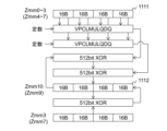
図11A及び図11Bは、実施例1のストレージシステム120におけるCRC計算の並列方法を示す図である。この方法は、図4のステップS405とステップS406、図5のステップS503とステップS504におけるCRC計算に適用される。
Figures 11A and 11B are diagrams showing a parallel method for CRC calculation in the
図11Aは、CPU133による4つのデータブロックのCRC計算の並列処理における、バイナリデータの短縮処理(図10Bの処理全体に相当)の方法を示す。
Figure 11A shows a method for shortening binary data (corresponding to the entire process in Figure 10B) in parallel processing of CRC calculations of four data blocks by the
Zmmレジスタ1111は、図7~9を用いて説明した4つのデータブロックのXTS暗号化/復号の並列処理において、暗号化/復号の入力データ又は暗号化/復号の出力データの構成要素である、4つのデータブロックに対応する16バイトのデータを保持するレジスタである。具体的には、XTS暗号化/復号の入力データの場合はZmm0レジスタ、Zmm1レジスタ、Zmm2レジスタ、又はZmm3レジスタを示し、XTS暗号化/復号の出力データの場合はZmm4レジスタ、Zmm5レジスタ、Zmm6レジスタ、又はZmm7レジスタを示す。
本発明は、Zmmレジスタ1111がXTS暗号化/復号のために保持しているデータを用いて、CRC計算の対象データの短縮処理を並列で行う。Zmmレジスタ1111の16バイトのデータは、図10BのH(x)とL(x)が示す2つの64ビット値を並べた128ビット値に相当する。
The present invention performs parallel shortening of the data subject to CRC calculation using the data held in
Zmmレジスタ1112は、短縮処理の途中、又は短縮処理後に得られる、4つのデータブロックの128ビットのバイナリデータを保持するレジスタである。具体的には、XTS暗号化/復号の入力データのCRC計算の場合はZmm10レジスタを示し、XTS暗号化/復号の出力データのCRC計算の場合はZmm9レジスタを示す。
まず、CPU133は、(PP1)VPCLMULQDQ命令を実行することによって、Zmmレジスタ1111の16バイトのデータの上位64ビットに同じ定数を乗じる。演算結果として128ビットのデータが4つ出力される。次に、CPU133は、(PP2)VPCLMULQDQ命令を実行することによって、Zmmレジスタの各16バイトのデータの下位64ビットに同じ定数を乗じる。演算結果として128ビットのデーが4つ出力される。CPU133は、(PP3)これら2つの結果とZmmレジスタ1112との排他的論理和を算出し、その結果を再びZmmレジスタ1112に格納する。(PP1)~(PP3)の処理が1回の短縮処理に対応する。
First, CPU 133 (PP1) executes the VPCLMULQDQ instruction to multiply the upper 64 bits of the 16 bytes of data in
CPU133は、4つのデータブロックのXTS暗号化/復号の並列処理において、Zmmレジスタ1111に次の16バイトのデータが格納された場合、(PP1)~(PP3)で示す短縮処理を繰り返す。CPU133は、短縮処理を31回実行し、Zmmレジスタ1111にブロック最後の16バイトのデータ(つまり、Group7の4つ目)が格納された場合、Zmmレジスタ1111の値とZmmレジスタ1112との排他的論理和を算出し、その結果を再びZmmレジスタ1112に格納する。
When the next 16 bytes of data are stored in
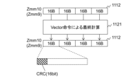
図11Bは、CPU133による4ブロックデータのCRC計算の並列処理における、最終計算(図10Bの最終処理)の方法を示す。
Figure 11B shows the method of the final calculation (final processing in Figure 10B) in the parallel processing of CRC calculation of four block data by
Zmmレジスタ1112は、4つのデータブロックの、最終計算に用いる128ビットのバイナリデータを保持している。本発明はCRC計算の最終計算を、このZmmレジスタ1112に保持したデータを利用して並列で行う。ここで並列の最終計算1121は、図10Bの最終計算に用いるCPU命令を、対応するVector命令に置き換えて実装する。すなわち、XOR命令はVector XOR命令、PCLMULQDQ命令はVPCLMULQDQ命令に置き換える。Barrett Reductionを構成する各命令も同様に、それに対応するVector命令に置き換える。最終的なCRC計算の結果は、Zmmレジスタ1112に格納する。具体的には、XTS暗号化/復号の入力データのCRC計算の場合はZmm10レジスタを示し、XTS暗号化/復号の出力データのCRC計算の場合はZmm9レジスタを示す。4つのCRC計算の結果が格納される位置は、Zmmレジスタ1112の各16バイトの先頭16ビットである。なお、CRC計算の完了時点で、各16バイトの残り部分(112ビット)は未使用である。
図12A及び図12Bは、実施例1のストレージシステム120における4つのデータブロックのDIFの並列的な生成方法を説明する図である。
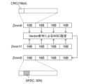
Figures 12A and 12B are diagrams illustrating a method for generating DIFs in parallel for four data blocks in
図12Aは、図11に示す方法により、XTS暗号化/復号の出力データから並列的に計算された4つのCRCを保持するZmm9レジスタに対して、CPU133が各CRCの後続部に1バイト(8ビット)のWSCを並列的に付加する方法を示す。
Figure 12A shows how the
付加するWSCは、図3を用いて説明したように、先頭ブロックのHEAD301は1、非先頭ブロックのHEAD301は0とし、終端ブロックのTAIL302は1、非終端ブロックのTAIL302は0とし、すべてのデータブロックのSQNは共通の6ビット値とする。この設定規則に基づくWSCを含む512ビットパタン(ただし、ATAG(1)233、243の各8ビットには00hが設定される。)を保持するZmm11レジスタを用意し、これをZmm9レジスタの各CRCの後の8ビット部分のみに重ね書きする。重ね書きには、例えば、ビットマスク付きMOV命令をVector化した命令を使用する。その結果、Zmm9レジスタはCRCとWSCの組を4つ格納される。
As explained with reference to FIG. 3, the WSC to be added is such that
例えば、ライト/リードするユーザデータのサイズが128Kバイト(256ブロック)の場合、WSCの付加の並列処理は64回行う必要がある。1回目の付加で、先頭ブロックのDIFのWSCのHEAD301には1が設定され、64回目の付加で、終端ブロックのDIFのWSCのTAIL302には1が設定される。その他のHEAD301とTAIL302には0が設定される。
For example, if the size of the user data to be written/read is 128 KB (256 blocks), the parallel processing of adding WSCs must be performed 64 times. In the first addition, 1 is set to HEAD 301 of the WSC in the DIF of the first block, and in the 64th addition, 1 is set to
図12Bは、CPU133がZmm9レジスタに対して、各ATAG(1)233、243の後続部に4バイトのRTAG234、244を並列的に付加する方法を示す。
Figure 12B shows how the
付加するRTAG234、244は、昇順に並んだ4つのデータブロックのアドレスである。この設定規則に基づくRTAG234、244を含む512ビットパタンを格納するZmm12レジスタを用意し、これをZmm9レジスタの各ATAG(1)233、234の後の4バイト部分のみに重ね書きする。重ね書きには、例えば、ビットマスク付きMOV命令をVector化した命令を使用する。その結果、Zmm9レジスタにはDIF(つまり、CRC、WSC、RTAGの組)が4つ格納される。これは図9において、付加する4つのDIFを保持するZmm9レジスタに相当する。このZmm9レジスタからDRAM134への格納命令によって、4つの出力データブロックの各終端にDIFが付加される。
The
以上に述べた、並列的なDIF生成の方法は、図4のS411及び図5のS509に適用する。 The parallel DIF generation method described above is applied to S411 in FIG. 4 and S509 in FIG. 5.
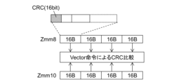
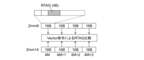
図13A、図13B、及び図13Cは、実施例1のストレージシステム120における4つのデータブロックのDIFの並列的な検査方法を説明する図である。
Figures 13A, 13B, and 13C are diagrams illustrating a method for parallel inspection of the DIFs of four data blocks in the
図13A、図13B、及び図13Cにおいて、Zmm8レジスタは、図8でXTS暗号化/復号の入力データの各データブロックに後続するDIF(合わせて4つ)を格納するZmmレジスタである。 In Figures 13A, 13B, and 13C, the Zmm8 register is a Zmm register that stores the DIFs (four in total) that follow each data block of the input data for XTS encryption/decryption in Figure 8.
図13Aは、Zmm8レジスタに対を用いた、4つのCRCの並列的な検査方法を示す。 Figure 13A shows a method for checking four CRCs in parallel using pairs in the Zmm8 register.
図11に示す方法により、Zmm10レジスタは、XTS暗号化/復号の入力データから並列的に計算された4つのCRCを保持する。これらの各CRCが、Zmm8レジスタに格納される各CRCと一致するか否かを並列に検査する。当該検査には、例えば、ビットマスク付きCOMPARE命令をVector化した命令が使用される。その結果、4つの比較結果がすべて一致となればCRC検査は成功である。この検査方法は、図4のステップS408及び図5のステップS506に適用する。 Using the method shown in FIG. 11, the Zmm10 register holds four CRCs calculated in parallel from the input data for XTS encryption/decryption. Each of these CRCs is checked in parallel to see if it matches each CRC stored in the Zmm8 register. For this check, for example, an instruction that is a vectorized version of a bit-masked COMPARE instruction is used. If all four comparison results match, the CRC check is successful. This check method is applied to step S408 in FIG. 4 and step S506 in FIG. 5.
図13Bは、Zmm8レジスタを用いた4つのWSCの並列的な検査方法を示す。 Figure 13B shows a method for testing four WSCs in parallel using Zmm8 registers.
Zmm13レジスタは、下位48バイトにはZmm8レジスタの内容を16バイト右方向にシフトしたもの、上位16バイトには前回検査した第4のブロック(つまり、アドレスが4N+3)のDIFを保持する。これらの各WSCのSQNが、Zmm8レジスタのWSCのSQNと一致するか否かを並列に検査する。当該検査には、例えば、ビットマスク付きCOMPARE命令をVector化した命令を使用される。
The lower 48 bytes of the Zmm13 register hold the contents of the Zmm8 register shifted 16 bytes to the right, and the upper 16 bytes hold the DIF of the fourth block (i.e.,
ただし、図3Cの表320に示す(R3)、(R4)の条件に合わないWSCのSQNの検査は行われない。この場合、例えば、COMPARE命令のマスクパラメタを部分的にゼロにする。 However, the SQN of a WSC that does not meet the conditions (R3) or (R4) shown in table 320 in FIG. 3C is not inspected. In this case, for example, the mask parameter of the COMPARE instruction is partially set to zero.
WSCの検査後に、Zmm8レジスタ上の、第4のブロックのDIFを含む下位16バイトを次回のWSC検査のためにレジスタに退避する。その結果、有効なSQN比較(最大で4つ)の結果がすべて一致すればWSC検査は成功である。このように、Zmm13レジスタに、1ブロック分シフトしたWSCを保持することにより、1回のVector COMPARE命令を実行することによって、自WSCと前WSCとのSQN比較を4つ同時に実行できる。この検査方法は、図5のステップS507に適用する。 After checking the WSC, the lower 16 bytes including the DIF of the fourth block in the Zmm8 register are saved to a register for the next WSC check. As a result, if all valid SQN comparisons (up to four) result in a match, the WSC check is successful. In this way, by holding the WSC shifted by one block in the Zmm13 register, four SQN comparisons between the current WSC and the previous WSC can be performed simultaneously by executing one Vector COMPARE command. This check method is applied to step S507 in Figure 5.
例えば、ライト/リードするユーザデータのサイズが128Kバイト(256ブロック)の場合、4つの暗号化データブロックのWSCの並列検査は64回行う必要がある。Zmm8レジスタ上の、第4のブロックのDIFを含む下位16バイトは、1回目~63回目の検査で退避され、2回目~64回目の検査でZmm13レジスタの上位16バイトに転送される。1回目の検査でZmm13レジスタの上位16バイトには何も転送しないが、最初のWSCは検査されないため、この場所には無効な値が含まれていてよい。 For example, if the size of the user data to be written/read is 128 KB (256 blocks), then 64 parallel checks of the WSC of the four encrypted data blocks must be performed. The lower 16 bytes of the Zmm8 register, including the DIF of the fourth block, are saved during the first through 63rd checks, and are transferred to the upper 16 bytes of the Zmm13 register during the second through 64th checks. Nothing is transferred to the upper 16 bytes of the Zmm13 register during the first check, but because the first WSC is not checked, this location may contain an invalid value.
図13Cは、Zmm8レジスタを用いた4つのRTAGの並列的な検査方法を示す。 Figure 13C shows a method for testing four RTAGs in parallel using Zmm8 registers.
Zmm14レジスタは、昇順に並んだ4つのアドレスを保持する。これらの各アドレスが、Zmm8レジスタ上の対応するRTAGと一致するかを並列に検査する。当該検査には、例えば、ビットマスク付きCOMPARE命令をVector化した命令が使用される。その結果、4つのアドレスがすべて一致となればRTAG検査は成功である。この検査方法は、図4のステップS409及び図5のステップS508に適用する。 The Zmm14 register holds four addresses arranged in ascending order. Each of these addresses is checked in parallel to see if it matches the corresponding RTAG in the Zmm8 register. For this check, for example, an instruction that is a vectorized version of a bit-masked COMPARE instruction is used. As a result, if all four addresses match, the RTAG check is successful. This check method is applied to step S409 in FIG. 4 and step S508 in FIG. 5.
図12と図13において、DIFの検査/生成に用いられるZmmレジスタの番号(Zmm11レジスタ、Zmm12レジスタ、Zmm13レジスタ、Zmm14レジスタ)は一例であって、他のレジスタ番号でもよい。 In Figures 12 and 13, the numbers of the Zmm registers used to inspect/generate DIF (register Zmm11, register Zmm12, register Zmm13, and register Zmm14) are merely examples, and other register numbers may be used.
以上、本発明を適用したストレージシステム120のCPU133は、ライト/リード処理において、512ビットのZmmレジスタとVector命令とを用い、XTS暗号化/復号、CRC計算、DIF生成、及びDIF検査を、並列で実行できる。また、上に述べたZmmレジスタの使い方に従えば、ZmmレジスタとDRAM134との間のロード/格納の回数は必要最小限に抑えられ、データ演算サイクル以外のオーバヘッドサイクルが最小化される。
As described above, the
なお、ライト/リードするユーザデータのサイズが、2048Uバイト(Uは整数)の場合、4ブロック並列のライト/リード処理をU回行う必要があるが、ステップS401のデータ受信、ステップS412のデータライト、ステップS501のデータリード、ステップS512のデータ送信は、それぞれU回に分けて実施せず、1回にまとめて実施してもよい。 When the size of the user data to be written/read is 2048U bytes (U is an integer), it is necessary to perform U times of parallel write/read processing of four blocks, but the data reception in step S401, the data write in step S412, the data read in step S501, and the data transmission in step S512 may be performed all at once instead of being divided into U times.
なお、本発明は、4つの処理データを保持する512ビットのZmmレジスタの代わりに、2つの処理データを保持する256ビットのYmmレジスタを用いてもよい。その場合、上に述べた方法と同様に、Ymmレジスタに対するVector命令を適用して、XTS暗号化/復号、CRC計算、DIF生成、DIF検査を、すべて2ブロック並列で処理することができる。 In addition, the present invention may use a 256-bit Ymm register that holds two pieces of processing data instead of a 512-bit Zmm register that holds four pieces of processing data. In that case, similar to the method described above, by applying a Vector instruction to the Ymm register, XTS encryption/decryption, CRC calculation, DIF generation, and DIF checking can all be processed in two blocks in parallel.
本発明は、ホスト計算機110から受信したユーザデータを暗号化してストレージデバイスに格納するライト処理、及びストレージデバイスに格納された暗号化ユーザデータを復号してホスト計算機110に送信するリード処理を、従来よりも高速に実行することができるという効果を奏する。
The present invention has the effect of enabling faster execution of write processing, in which user data received from a
以上、本発明の一実施例を説明したが、これは本発明の説明のための例示であって、本発明の範囲をこの実施例にのみ限定する趣旨ではない。すなわち、本発明は、他の種々の形態でも実施する事が可能である。 One embodiment of the present invention has been described above, but this is merely an example for the purpose of explaining the present invention, and is not intended to limit the scope of the present invention to only this embodiment. In other words, the present invention can be implemented in various other forms.
110 ホスト計算機
120 ストレージシステム
130 ストレージコントローラ
131 FE I/F
132 BE I/F
133 CPU
134 DRAM
140 ストレージデバイス
110
132 BE I/F
133 CPU
134 DRAM
140 Storage device
Claims (21)
プロセッサ、前記プロセッサに接続されるメモリ、前記プロセッサに接続される記憶媒体、及び前記プロセッサに接続される接続インタフェースを備え、
前記プロセッサは、
複数のレジスタを有し、
前記ユーザデータの書き込みリクエストを受信し、
前記書き込みリクエストに従って書き込まれる前記ユーザデータを前記メモリに格納し、
前記複数のレジスタを用いて、複数の暗号化データブロックを含む暗号化ユーザデータを生成する暗号化処理を実行し、
2以上の第1データ保全性フィールドを第1レジスタに格納し、
前記第1レジスタに格納された前記2以上の前記第1データ保全性フィールドの各々に、前記暗号化データブロックの格納位置を示す第1アドレスを設定する設定処理を並列に実行し、
前記暗号化ユーザデータに含まれる前記複数の暗号化データブロックの各々に、前記第1アドレスが設定された第1データ保全性フィールドを付加し、
前記暗号化ユーザデータを前記記憶媒体に格納する、
ことを特徴とする計算機。 A computer that writes and reads user data including a plurality of data blocks, comprising:
a processor, a memory connected to the processor, a storage medium connected to the processor, and a connection interface connected to the processor;
The processor,
A plurality of registers are included.
receiving a request to write the user data;
storing the user data written in accordance with the write request in the memory;
performing an encryption process using the plurality of registers to generate encrypted user data including a plurality of encrypted data blocks;
storing two or more first data integrity fields in a first register;
performing in parallel a setting process for setting a first address indicating a storage location of the encrypted data block in each of the two or more first data integrity fields stored in the first register;
adding a first data integrity field, the first address being set to each of the plurality of encrypted data blocks included in the encrypted user data;
storing the encrypted user data on the storage medium ;
1. A computer comprising:
前記第1データ保全性フィールドには、前記データブロックの書き込みの世代を表す第1世代番号を設定することができ、A first generation number representing a generation of writing of the data block can be set in the first data integrity field,
前記プロセッサは、前記第1レジスタに格納された前記2以上の前記第1データ保全性フィールドの各々に、前記暗号化データブロックの前記第1世代番号を設定する設定処理を並列に実行することを特徴とする計算機。a first data integrity field storing means for storing a first generation number of the encrypted data block in each of the first data integrity fields stored in the first register, the first generation number being set in the first data integrity field in parallel;
前記第1データ保全性フィールドは第1誤り符号を含むことを特徴とする計算機。The first data integrity field includes a first error code.
前記プロセッサは、
前記暗号化ユーザデータの読み出しリクエストを受信し、
前記記憶媒体から、前記読み出しリクエストによって指定された前記暗号化ユーザデータを読み出し、前記メモリに格納し、
前記複数のレジスタを用いて、前記暗号化ユーザデータを復号する復号処理を実行し、
第2レジスタに2以上の第2データ保全性フィールドを格納し、
前記第2レジスタに格納された前記2以上の前記第2データ保全性フィールドの各々に、前記暗号化データブロックの格納位置を示す第2アドレスを設定する設定処理を並列に実行し、
復号された前記ユーザデータに含まれる前記複数のデータブロックの各々に、前記第2アドレスが設定された第2データ保全性フィールドを付加し、前記メモリに格納する、
ことを特徴とする計算機。 3. The computer of claim 2,
The processor,
receiving a request to read the encrypted user data;
reading from said storage medium said encrypted user data specified by said read request and storing said encrypted user data in said memory;
performing a decryption process for decrypting the encrypted user data using the plurality of registers;
storing two or more second data integrity fields in a second register;
performing in parallel a setting process for setting a second address indicating a storage location of the encrypted data block in each of the two or more second data integrity fields stored in the second register;
adding a second data integrity field, in which the second address is set, to each of the plurality of data blocks included in the decrypted user data, and storing the data in the memory;
1. A computer comprising:
前記第2データ保全性フィールドには、前記データブロックの書き込みの世代を表す第2世代番号を設定することができ、A second generation number representing a generation of writing of the data block can be set in the second data integrity field,
前記プロセッサは、前記第2レジスタに格納された前記2以上の前記第2データ保全性フィールドの各々に、前記データブロックの前記第2世代番号を設定する設定処理を並列に実行することを特徴とする計算機。a second data integrity field storing means for storing a second generation number of the data block in each of the two or more second data integrity fields stored in the second register, the second generation number being set in the second data integrity field in parallel;
前記プロセッサは、The processor,
SIMD命令を用いて、前記第1レジスタに格納された前記2以上の前記第1データ保全性フィールドの各々に前記第1アドレスを設定する設定処理を並列で実行し、performing a setting operation in parallel using a SIMD instruction to set each of the two or more first data integrity fields stored in the first register to the first address;
前記SIMD命令を用いて、前記第1レジスタに格納された前記2以上の前記第1データ保全性フィールドの各々に前記第1世代番号を設定する設定処理を並列で実行し、executing, in parallel, a setting process for setting the first generation number in each of the two or more first data integrity fields stored in the first register using the SIMD instruction;
前記SIMD命令を用いて、前記第2レジスタに格納された前記2以上の前記第2データ保全性フィールドの各々に前記第2アドレスを設定する設定処理を並列で実行し、performing a setting operation in parallel using the SIMD instruction to set the second address in each of the two or more second data integrity fields stored in the second register;
前記SIMD命令を用いて、前記第2レジスタに格納された前記2以上の前記第2データ保全性フィールドの各々に前記第2世代番号を設定する設定処理を並列で実行することを特徴とする計算機。a setting process for setting the second generation number in each of the two or more second data integrity fields stored in the second register in parallel using the SIMD instruction.
前記第2データ保全性フィールドは第1誤り符号を含むことを特徴とする計算機。The second data integrity field includes a first error code.
プロセッサ、前記プロセッサに接続されるメモリ、前記プロセッサに接続される記憶媒体、及び前記プロセッサに接続される接続インタフェースを備え、
前記プロセッサは、
複数のレジスタを有し、
前記ユーザデータの書き込みリクエストを受信し、
前記書き込みリクエストに従って書き込まれる前記ユーザデータを前記メモリに格納し、
前記複数のレジスタを用いて、複数の暗号化データブロックを含む暗号化ユーザデータを生成する暗号化処理を実行し、
前記複数のレジスタを用いて、前記ユーザデータの破損を検出するための第1検査処理を実行し、
前記暗号化ユーザデータを前記記憶媒体に格納し、
前記ユーザデータに含まれる前記複数のデータブロックの各々には、第1誤り符号を含む第1データ保全性フィールドが付加され、
前記暗号化処理では、
所定の数の前記データブロックから、前記データブロックの一部である部分データを読み出し、第1レジスタに格納する第1処理と、
前記第1レジスタに格納される前記部分データを暗号化した暗号化部分データを第2レジスタに格納する第2処理と、
前記第1レジスタに格納される前記部分データを用いて、前記第1誤り符号を生成するための第1演算を実行し、前記第1演算の結果を第3レジスタに格納する第3処理と、
が繰り返し実行され、
前記第1検査処理は、
第4レジスタに、所定の数の前記データブロックの前記第1データ保全性フィールドを読み出す処理と、
前記第3レジスタに格納される前記第1誤り符号と、前記第4レジスタに格納される前記第1データ保全性フィールドに含まれる前記第1誤り符号とを比較することによって、前記メモリから読み出された前記ユーザデータが破損しているか否かを判定する処理と、
を含むことを特徴とする計算機。 A computer that writes and reads user data including a plurality of data blocks, comprising:
a processor, a memory connected to the processor, a storage medium connected to the processor, and a connection interface connected to the processor;
The processor,
A plurality of registers are included.
receiving a request to write the user data;
storing the user data written in accordance with the write request in the memory;
performing an encryption process using the plurality of registers to generate encrypted user data including a plurality of encrypted data blocks;
performing a first test process using the plurality of registers to detect corruption of the user data;
storing the encrypted user data on the storage medium;
a first data integrity field including a first error code is added to each of the plurality of data blocks included in the user data;
In the encryption process,
a first process of reading partial data, which is a part of the data blocks, from a predetermined number of the data blocks and storing the partial data in a first register;
a second process of encrypting the partial data stored in the first register and storing the encrypted partial data in a second register;
a third process of executing a first operation for generating the first error-correcting code by using the partial data stored in the first register, and storing a result of the first operation in a third register;
is executed repeatedly,
The first inspection process includes:
reading said first data integrity field of a predetermined number of said data blocks into a fourth register;
determining whether the user data read from the memory is corrupted by comparing the first error code stored in the third register with the first error code included in the first data integrity field stored in the fourth register;
23. A computer comprising:
前記第1データ保全性フィールドは、前記データブロックの格納位置を示す第1アドレスを含み、
前記第1検査処理は、
第5レジスタに、所定の数の前記データブロックの前記第1アドレスを読み出す処理と、
前記第5レジスタに格納される前記第1アドレスと、前記第4レジスタに格納される前記第1データ保全性フィールドに含まれる前記第1アドレスとを比較することによって、前記メモリから読み出された前記ユーザデータが破損しているか否かを判定する処理と、
を含むことを特徴とする計算機。 9. The computer of claim 8,
the first data integrity field includes a first address indicating a storage location of the data block;
The first inspection process includes:
reading the first addresses of a predetermined number of the data blocks into a fifth register;
determining whether the user data read from the memory is corrupted by comparing the first address stored in the fifth register with the first address included in the first data integrity field stored in the fourth register;
23. A computer comprising:
前記プロセッサは、
前記暗号化ユーザデータの読み出しリクエストを受信し、
前記記憶媒体から、前記読み出しリクエストによって指定された前記暗号化ユーザデータを読み出し、前記メモリに格納し、
前記複数のレジスタを用いて、前記暗号化ユーザデータを復号する復号処理を実行し、
前記複数のレジスタを用いて、前記暗号化ユーザデータの破損を検出するための第2検査処理を実行し、
前記ユーザデータを前記メモリに格納し、
前記暗号化ユーザデータに含まれる前記複数の暗号化データブロックの各々には、第2誤り符号を含む第2データ保全性フィールドが付加され、
前記復号処理では、
所定の数の前記暗号化データブロックから、前記暗号化データブロックの一部である部分暗号化データを読み出し、第6レジスタに格納する第8処理と、
前記第6レジスタに格納される前記部分暗号化データを復号した前記部分データを第7レジスタに格納する第9処理と、
前記第6レジスタに格納される前記暗号化部分データを用いて、前記第2誤り符号を生成するための第2演算を実行し、前記第2演算の結果を第8レジスタに格納する第10処理と、
が繰り返し実行され、
前記第2検査処理は、
第9レジスタに、所定の数の前記暗号化データブロックの前記第2データ保全性フィールドを読み出す処理と、
前記第8レジスタに格納される前記第2誤り符号と、前記第9レジスタに格納される前記第1データ保全性フィールドに含まれる前記第2誤り符号とを比較することによって、前記記憶媒体から読み出された前記暗号化ユーザデータが破損しているか否かを判定する処理と、
を含むことを特徴とする計算機。 10. The computer of claim 9,
The processor,
receiving a request to read the encrypted user data;
reading from said storage medium said encrypted user data specified by said read request and storing said encrypted user data in said memory;
performing a decryption process for decrypting the encrypted user data using the plurality of registers;
performing a second checking process using the plurality of registers to detect corruption of the encrypted user data;
storing said user data in said memory;
a second data integrity field including a second error code is added to each of the plurality of encrypted data blocks included in the encrypted user data;
In the decoding process,
an eighth process of reading partial encrypted data, which is a part of the encrypted data block, from a predetermined number of the encrypted data blocks and storing the partial encrypted data in a sixth register;
a ninth process of storing the partial data obtained by decrypting the partially encrypted data stored in the sixth register in a seventh register;
a tenth process of performing a second operation for generating the second error code by using the encrypted partial data stored in the sixth register, and storing a result of the second operation in an eighth register;
is executed repeatedly,
The second inspection process includes:
reading said second data integrity field of a predetermined number of said encrypted data blocks into a ninth register;
determining whether the encrypted user data read from the storage medium is corrupted by comparing the second error code stored in the eighth register with the second error code included in the first data integrity field stored in the ninth register;
23. A computer comprising:
前記第2データ保全性フィールドは、前記暗号化データブロックの格納位置を示す第2アドレスを含み、
前記第2検査処理は、
第10レジスタに、所定の数の前記暗号化データブロックに対応する前記第2アドレスを読み出す処理と、
前記第9レジスタに格納される前記第2データ保全性フィールドに含まれる前記第2アドレスと、前記第10レジスタに格納される前記第2アドレスとを比較することによって、前記記憶媒体から読み出された前記暗号化ユーザデータが破損しているか否かを判定する処理と、
を含むことを特徴とする計算機。 11. The computer of claim 10,
the second data integrity field includes a second address indicating a storage location of the encrypted data block;
The second inspection process includes:
reading, into a tenth register, the second addresses corresponding to a predetermined number of the encrypted data blocks;
determining whether the encrypted user data read from the storage medium is corrupted by comparing the second address contained in the second data integrity field stored in the ninth register with the second address stored in the tenth register;
23. A computer comprising:
前記第2データ保全性フィールドは、前記データブロックの書き込みの世代を表す第2世代番号を含み、
前記第2検査処理は、
第11レジスタに、所定の数の前記暗号化データブロックに対応する前記第2世代番号を読み出す処理と、
前記第9レジスタに格納される前記第1データ保全性フィールドに含まれる前記第2世代番号と、前記第11レジスタに格納される前記第2世代番号とを比較することによって、前記記憶媒体から読み出された前記暗号化ユーザデータが破損しているか否かを判定する処理と、
を含むことを特徴とする計算機。 12. The computer of claim 11,
the second data integrity field includes a second generation number representing a generation of writing of the data block;
The second inspection process includes:
reading, into an eleventh register, the second generation numbers corresponding to a predetermined number of the encrypted data blocks;
determining whether the encrypted user data read from the storage medium is corrupted by comparing the second generation number included in the first data integrity field stored in the ninth register with the second generation number stored in the eleventh register;
23. A computer comprising:
前記プロセッサは、SIMD命令を用いて、前記複数のデータブロック及び前記複数の暗号化データブロックに対する処理を並列で実行することを特徴とする計算機。 13. The computer of claim 12,
The processor executes processing on the plurality of data blocks and the plurality of encrypted data blocks in parallel using SIMD instructions.
前記計算機は、プロセッサ、前記プロセッサに接続されるメモリ、前記プロセッサに接続される記憶媒体、及び前記プロセッサに接続される接続インタフェースを有し、
前記プロセッサは、複数のレジスタを有し、
前記データ処理方法は、
前記プロセッサが、前記ユーザデータの書き込みリクエストを受信するステップと、
前記プロセッサが、前記書き込みリクエストに従って書き込まれる前記ユーザデータを前記メモリに格納するステップと、
前記プロセッサが、前記複数のレジスタを用いて、複数の暗号化データブロックを含む暗号化ユーザデータを生成する暗号化処理を実行するステップと、
前記プロセッサが、前記複数のレジスタを用いて、前記ユーザデータの破損を検出するための検査処理を実行するステップと、
前記プロセッサが、前記暗号化ユーザデータに含まれる前記複数の暗号化データブロックの各々に、第1誤り符号を含む第1データ保全性フィールドを付加するステップと、
前記プロセッサが、前記暗号化ユーザデータを前記記憶媒体に格納するステップと、
を含み、
前記暗号化処理では、
所定の数の前記データブロックから、前記データブロックの一部である部分データを読み出し、第1レジスタに格納する第1処理と、
前記第1レジスタに格納される前記部分データを暗号化した暗号化部分データを第2レジスタに格納する第2処理と、
前記第2レジスタに格納される前記暗号化部分データを用いて、前記第1誤り符号を算出するための第1演算を実行し、前記第1演算の結果を第3レジスタに格納する第3処理と、
が繰り返し実行され、
前記検査処理は、
第4レジスタに、所定の数の前記データブロックの前記第1データ保全性フィールドを読み出す処理と、
前記第3レジスタに格納される前記第1誤り符号と、前記第4レジスタに格納される前記第1データ保全性フィールドに含まれる前記第1誤り符号とを比較することによって、前記メモリから読み出された前記ユーザデータが破損しているか否かを判定する処理と、
を含むことを特徴とするデータ処理方法。 1. A computer-implemented data processing method for writing and reading user data including a plurality of data blocks, comprising:
the computer includes a processor, a memory connected to the processor, a storage medium connected to the processor, and a connection interface connected to the processor;
The processor has a plurality of registers;
The data processing method includes:
receiving a request by the processor to write the user data;
storing, by the processor, in the memory, the user data to be written in accordance with the write request;
performing an encryption process using the plurality of registers to generate encrypted user data including a plurality of encrypted data blocks;
The processor executes a test process using the plurality of registers to detect corruption of the user data;
the processor appending a first data integrity field including a first error code to each of the plurality of encrypted data blocks included in the encrypted user data;
storing, by the processor, the encrypted user data on the storage medium;
Including,
In the encryption process,
a first process of reading partial data, which is a part of the data blocks, from a predetermined number of the data blocks and storing the partial data in a first register;
a second process of encrypting the partial data stored in the first register and storing the encrypted partial data in a second register;
a third process of performing a first operation for calculating the first error code by using the encrypted partial data stored in the second register, and storing a result of the first operation in a third register;
is executed repeatedly,
The inspection process includes:
reading said first data integrity field of a predetermined number of said data blocks into a fourth register;
determining whether the user data read from the memory is corrupted by comparing the first error code stored in the third register with the first error code included in the first data integrity field stored in the fourth register;
13. A data processing method comprising:
プロセッサ、前記プロセッサに接続されるメモリ、前記プロセッサに接続される記憶媒体、及び前記プロセッサに接続される接続インタフェースを備え、a processor, a memory connected to the processor, a storage medium connected to the processor, and a connection interface connected to the processor;
前記プロセッサは、The processor,
複数のレジスタを有し、A plurality of registers are included.
前記ユーザデータの書き込みリクエストを受信し、receiving a request to write the user data;
前記書き込みリクエストに従って書き込まれる前記ユーザデータを前記メモリに格納し、storing the user data written in accordance with the write request in the memory;
前記複数のレジスタを用いて、複数の暗号化データブロックを含む暗号化ユーザデータを生成する暗号化処理を実行し、performing an encryption process using the plurality of registers to generate encrypted user data including a plurality of encrypted data blocks;
前記暗号化ユーザデータに含まれる前記複数の暗号化データブロックの各々に、第1誤り符号を含む第1データ保全性フィールドを付加し、appending a first data integrity field including a first error code to each of the plurality of encrypted data blocks included in the encrypted user data;
前記暗号化ユーザデータを前記記憶媒体に格納し、storing the encrypted user data on the storage medium;
前記暗号化処理では、In the encryption process,
所定の数の前記データブロックから、前記データブロックの一部である部分データを読み出し、第1レジスタに格納する第1処理と、a first process of reading partial data, which is a part of the data blocks, from a predetermined number of the data blocks and storing the partial data in a first register;
前記第1レジスタに格納される前記部分データを暗号化した暗号化部分データを第2レジスタに格納する第2処理と、a second process of encrypting the partial data stored in the first register and storing the encrypted partial data in a second register;
前記第2レジスタに格納される前記暗号化部分データを用いて、前記第1誤り符号を算出するための第1演算を実行し、前記第1演算の結果を第3レジスタに格納する第3処理と、a third process of performing a first operation for calculating the first error code by using the encrypted partial data stored in the second register, and storing a result of the first operation in a third register;
が繰り返し実行され、is executed repeatedly,
前記第1データ保全性フィールドには、前記暗号化データブロックの格納位置を示す第1アドレスを設定することができ、A first address indicating a storage location of the encrypted data block may be set in the first data integrity field,
前記プロセッサは、The processor,
第4レジスタに、所定の数の前記暗号化データブロックの前記第1誤り符号を読み出し、reading the first error code for a predetermined number of the encrypted data blocks into a fourth register;
前記第4レジスタに格納される前記第1誤り符号に、当該第1誤り符号が付加される前記暗号化データブロックの前記第1アドレスを追加することによって、前記第1データ保全性フィールドを生成し、generating the first data integrity field by appending to the first error code stored in the fourth register the first address of the encrypted data block to which the first error code is to be appended;
前記第1データ保全性フィールドには、前記データブロックの書き込みの世代を表す第1世代番号を設定することができ、A first generation number representing a generation of writing of the data block can be set in the first data integrity field,
前記プロセッサは、前記第4レジスタに格納される前記第1誤り符号に、当該第1誤り符号が付加される前記暗号化データブロックの前記第1世代番号を追加することによって、前記第1データ保全性フィールドを生成することを特徴とする計算機。The processor generates the first data integrity field by adding the first generation number of the encrypted data block to which the first error code is added to the first error code stored in the fourth register.
前記プロセッサは、The processor,
前記暗号化ユーザデータの読み出しリクエストを受信し、receiving a request to read the encrypted user data;
前記記憶媒体から、前記読み出しリクエストによって指定された前記暗号化ユーザデータを読み出し、前記メモリに格納し、reading from said storage medium said encrypted user data specified by said read request and storing said encrypted user data in said memory;
前記複数のレジスタを用いて、前記暗号化ユーザデータを復号する復号処理を実行し、performing a decryption process for decrypting the encrypted user data using the plurality of registers;
復号された前記ユーザデータに含まれる前記複数のデータブロックの各々に、第2誤り符号を含む第2データ保全性フィールドを付加し、前記メモリに格納し、adding a second data integrity field including a second error code to each of the plurality of data blocks included in the decoded user data, and storing the second data integrity field in the memory;
前記復号処理では、In the decoding process,
所定の数の前記暗号化データブロックから、前記暗号化データブロックの一部である部分暗号化データを読み出し、第5レジスタに格納する第4処理と、a fourth process of reading partial encrypted data, which is a part of the encrypted data blocks, from a predetermined number of the encrypted data blocks and storing the partial encrypted data in a fifth register;
前記第5レジスタに格納される前記部分暗号化データを復号した前記部分データを第6レジスタに格納する第5処理と、a fifth process of decrypting the partial encrypted data stored in the fifth register and storing the partial data in a sixth register;
前記第6レジスタに格納される前記部分データを用いて、前記第2誤り符号を算出するための第2演算を実行し、前記第2演算の結果を第7レジスタに格納する第8処理と、an eighth process of performing a second operation for calculating the second error code by using the partial data stored in the sixth register, and storing a result of the second operation in a seventh register;
が繰り返し実行されることを特徴とする計算機。A computer characterized in that:
前記第2データ保全性フィールドには、前記暗号化データブロックの格納位置を示す第2アドレスを設定することができ、A second address indicating a storage location of the encrypted data block may be set in the second data integrity field,
前記プロセッサは、The processor,
第8レジスタに、所定の数の前記データブロックの前記第2誤り符号を読み出し、reading the second error codes of a predetermined number of the data blocks into an eighth register;
前記第8レジスタに格納される前記第2誤り符号に、当該第2誤り符号が付加される前記データブロックの前記第2アドレスを追加することによって、前記第2データ保全性フィールドを生成することを特徴とする計算機。generating the second data integrity field by appending to the second error code stored in the eighth register the second address of the data block to which the second error code is to be added.
前記第2データ保全性フィールドには、前記データブロックの書き込みの世代を表す第2世代番号を設定することができ、A second generation number representing a generation of writing of the data block can be set in the second data integrity field,
前記プロセッサは、前記第8レジスタに格納される前記第2誤り符号に、当該第2誤り符号が付加される前記データブロックの前記第2世代番号を追加することによって、前記第2データ保全性フィールドを生成することを特徴とする計算機。The processor generates the second data integrity field by adding the second generation number of the data block to which the second error code is added to the second error code stored in the eighth register.
前記プロセッサは、SIMD命令を用いて、前記複数のデータブロック及び前記複数の暗号化データブロックに対する処理を並列で実行することを特徴とする計算機。The processor executes processing on the plurality of data blocks and the plurality of encrypted data blocks in parallel using SIMD instructions.
前記計算機は、プロセッサ、前記プロセッサに接続されるメモリ、前記プロセッサに接続される記憶媒体、及び前記プロセッサに接続される接続インタフェースを備え、the computer includes a processor, a memory connected to the processor, a storage medium connected to the processor, and a connection interface connected to the processor;
前記プロセッサは、複数のレジスタを有し、The processor has a plurality of registers;
前記データ処理方法は、The data processing method includes:
前記プロセッサが、前記ユーザデータの書き込みリクエストを受信するステップと、receiving a request by the processor to write the user data;
前記プロセッサが、前記書き込みリクエストに従って書き込まれる前記ユーザデータを前記メモリに格納するステップと、storing, by the processor, in the memory, the user data to be written in accordance with the write request;
前記プロセッサが、前記複数のレジスタを用いて、複数の暗号化データブロックを含む暗号化ユーザデータを生成する暗号化処理を実行するステップと、performing an encryption process using the plurality of registers to generate encrypted user data including a plurality of encrypted data blocks;
前記プロセッサが、2以上の第1データ保全性フィールドを第1レジスタに格納するステップと、storing two or more first data integrity fields in a first register by the processor;
前記プロセッサが、前記第1レジスタに格納された前記2以上の前記第1データ保全性フィールドの各々に、前記暗号化データブロックの格納位置を示す第1アドレスを設定する設定処理を並列に実行するステップと、a step of executing, in parallel, a setting process by the processor, setting a first address indicating a storage location of the encrypted data block in each of the two or more first data integrity fields stored in the first register;
前記プロセッサが、前記暗号化ユーザデータに含まれる前記複数の暗号化データブロックの各々に、前記第1アドレスが設定された第1データ保全性フィールドを付加するステップと、the processor appending a first data integrity field, the first address being set to each of the plurality of encrypted data blocks included in the encrypted user data;
前記プロセッサが、前記暗号化ユーザデータを前記記憶媒体に格納するステップと、storing, by the processor, the encrypted user data on the storage medium;
を含むことを特徴とするデータ処理方法。13. A data processing method comprising:
プロセッサ、前記プロセッサに接続されるメモリ、前記プロセッサに接続される記憶媒体、及び前記プロセッサに接続される接続インタフェースを有し、a processor, a memory connected to the processor, a storage medium connected to the processor, and a connection interface connected to the processor;
前記プロセッサは、複数のレジスタを有し、The processor has a plurality of registers;
前記データ処理方法は、The data processing method includes:
前記プロセッサが、前記ユーザデータの書き込みリクエストを受信するステップと、receiving a request by the processor to write the user data;
前記プロセッサが、前記書き込みリクエストに従って書き込まれる前記ユーザデータを前記メモリに格納するステップと、storing, by the processor, in the memory, the user data to be written in accordance with the write request;
前記プロセッサが、前記複数のレジスタを用いて、複数の暗号化データブロックを含む暗号化ユーザデータを生成する暗号化処理を実行するステップと、performing an encryption process using the plurality of registers to generate encrypted user data including a plurality of encrypted data blocks;
前記プロセッサが、前記暗号化ユーザデータに含まれる前記複数の暗号化データブロックの各々に、第1誤り符号を含む第1データ保全性フィールドを付加するステップと、the processor appending a first data integrity field including a first error code to each of the plurality of encrypted data blocks included in the encrypted user data;
前記プロセッサが、前記暗号化ユーザデータを前記記憶媒体に格納するステップと、storing, by the processor, the encrypted user data on the storage medium;
を含み、Including,
前記暗号化処理では、In the encryption process,
所定の数の前記データブロックから、前記データブロックの一部である部分データを読み出し、第1レジスタに格納する第1処理と、a first process of reading partial data, which is a part of the data blocks, from a predetermined number of the data blocks and storing the partial data in a first register;
前記第1レジスタに格納される前記部分データを暗号化した暗号化部分データを第2レジスタに格納する第2処理と、a second process of encrypting the partial data stored in the first register and storing the encrypted partial data in a second register;
前記第2レジスタに格納される前記暗号化部分データを用いて、前記第1誤り符号を算出するための第1演算を実行し、前記第1演算の結果を第3レジスタに格納する第3処理と、a third process of performing a first operation for calculating the first error code by using the encrypted partial data stored in the second register, and storing a result of the first operation in a third register;
が繰り返し実行され、is executed repeatedly,
前記第1データ保全性フィールドには、前記暗号化データブロックの格納位置を示す第1アドレスを設定することができ、A first address indicating a storage location of the encrypted data block may be set in the first data integrity field,
前記プロセッサは、The processor,
第4レジスタに、所定の数の前記暗号化データブロックの前記第1誤り符号を読み出し、reading the first error code for a predetermined number of the encrypted data blocks into a fourth register;
前記第4レジスタに格納される前記第1誤り符号に、当該第1誤り符号が付加される前記暗号化データブロックの前記第1アドレスを追加することによって、前記第1データ保全性フィールドを生成し、generating the first data integrity field by appending to the first error code stored in the fourth register the first address of the encrypted data block to which the first error code is to be appended;
前記第1データ保全性フィールドには、前記データブロックの書き込みの世代を表す第1世代番号を設定することができ、A first generation number representing a generation of writing of the data block can be set in the first data integrity field,
前記プロセッサは、前記第4レジスタに格納される前記第1誤り符号に、当該第1誤り符号が付加される前記暗号化データブロックの前記第1世代番号を追加することによって、前記第1データ保全性フィールドを生成することを特徴とするデータ処理方法。The data processing method, characterized in that the processor generates the first data integrity field by adding the first generation number of the encrypted data block to which the first error code is added to the first error code stored in the fourth register.
Priority Applications (2)
| Application Number | Priority Date | Filing Date | Title |
|---|---|---|---|
| JP2022141346A JP7583000B2 (en) | 2022-09-06 | 2022-09-06 | Computer and data processing method |
| US18/112,079 US12430475B2 (en) | 2022-09-06 | 2023-02-21 | Computer and data processing method |
Applications Claiming Priority (1)
| Application Number | Priority Date | Filing Date | Title |
|---|---|---|---|
| JP2022141346A JP7583000B2 (en) | 2022-09-06 | 2022-09-06 | Computer and data processing method |
Publications (2)
| Publication Number | Publication Date |
|---|---|
| JP2024036837A JP2024036837A (en) | 2024-03-18 |
| JP7583000B2 true JP7583000B2 (en) | 2024-11-13 |
Family
ID=90060644
Family Applications (1)
| Application Number | Title | Priority Date | Filing Date |
|---|---|---|---|
| JP2022141346A Active JP7583000B2 (en) | 2022-09-06 | 2022-09-06 | Computer and data processing method |
Country Status (2)
| Country | Link |
|---|---|
| US (1) | US12430475B2 (en) |
| JP (1) | JP7583000B2 (en) |
Citations (2)
| Publication number | Priority date | Publication date | Assignee | Title |
|---|---|---|---|---|
| US20210150074A1 (en) | 2020-12-23 | 2021-05-20 | Jose Niell | Vm encryption of block storage with end-to-end data integrity protection in a smartnic |
| JP2021132342A (en) | 2020-02-20 | 2021-09-09 | 株式会社日立製作所 | Storage system and encryption processing method |
Family Cites Families (4)
| Publication number | Priority date | Publication date | Assignee | Title |
|---|---|---|---|---|
| US8194854B2 (en) | 2008-02-27 | 2012-06-05 | Intel Corporation | Method and apparatus for optimizing advanced encryption standard (AES) encryption and decryption in parallel modes of operation |
| US10320558B2 (en) | 2012-05-07 | 2019-06-11 | Dark Signal Research, Llc | Method and apparatus for a secure and deduplicated write once read many virtual disk |
| CN116134421A (en) * | 2020-07-14 | 2023-05-16 | 微软技术许可有限责任公司 | Stream data to a multi-tile processing system |
| KR20220124923A (en) * | 2021-03-04 | 2022-09-14 | 삼성전자주식회사 | Storage devices and how they work |
-
2022
- 2022-09-06 JP JP2022141346A patent/JP7583000B2/en active Active
-
2023
- 2023-02-21 US US18/112,079 patent/US12430475B2/en active Active
Patent Citations (2)
| Publication number | Priority date | Publication date | Assignee | Title |
|---|---|---|---|---|
| JP2021132342A (en) | 2020-02-20 | 2021-09-09 | 株式会社日立製作所 | Storage system and encryption processing method |
| US20210150074A1 (en) | 2020-12-23 | 2021-05-20 | Jose Niell | Vm encryption of block storage with end-to-end data integrity protection in a smartnic |
Non-Patent Citations (2)
| Title |
|---|
| Keith Holt,"End-to-End Data Protection Justification",T10/03-224r0,T10 Technical Committee,2003年06月01日,[2024年5月17日検索],インターネット <URL:https://www.t10.org/ftp/t10/document.03/03-224r0.pdf> |
| 岡田 尚也,"ストレージシステム適用に向けたプロセッサPCIe性能の評価",FIT2016 第15回情報科学技術フォーラム 講演論文集 第1分冊,2016年 |
Also Published As
| Publication number | Publication date |
|---|---|
| US20240078347A1 (en) | 2024-03-07 |
| JP2024036837A (en) | 2024-03-18 |
| US12430475B2 (en) | 2025-09-30 |
Similar Documents
| Publication | Publication Date | Title |
|---|---|---|
| US11301344B2 (en) | Aggregate GHASH-based message authentication code (MAC) over multiple cachelines with incremental updates | |
| US10761928B2 (en) | Combined secure mac and device correction using encrypted parity with multi-key domains | |
| US9819659B2 (en) | Iterative data secret-sharing transformation | |
| CN103975302B (en) | Matrix multiply accumulate instruction | |
| US8150031B2 (en) | Method and apparatus to perform redundant array of independent disks (RAID) operations | |
| US8464125B2 (en) | Instruction-set architecture for programmable cyclic redundancy check (CRC) computations | |
| TWI642294B (en) | Computer program product , system and method of cipher message with authentication instruction | |
| US10235134B1 (en) | Rotating bit values while generating a large, non-compressible data stream | |
| US10656996B2 (en) | Integrated security and data redundancy | |
| CN109800103B (en) | Cryptographic System Memory Management | |
| US20120166909A1 (en) | Method and apparatus for increasing data reliability for raid operations | |
| US10038733B1 (en) | Generating a large, non-compressible data stream | |
| US12341532B2 (en) | Accelerated polynomial coding system and method | |
| US10163371B1 (en) | Rotating bit values based on a data structure while generating a large, non-compressible data stream | |
| JP2023130311A (en) | Method for protecting electronic computers from side channel attacks and electronic computers | |
| JP2010532880A (en) | System and method for processing data for data security | |
| JP7583000B2 (en) | Computer and data processing method | |
| CN117331746A (en) | Devices for redundant array of independent disks | |
| CN108572882B (en) | Data storage method and storage device | |
| CN117850667A (en) | Data protection and recovery | |
| JP5278115B2 (en) | Redundant code generation method and apparatus, data restoration method and apparatus, and RAID storage device | |
| US12130701B1 (en) | Residue-code-based error detection for cipher generation | |
| Klein et al. | Storage architecture with integrity, redundancy and encryption | |
| CN117331747A (en) | Uncached data transfer | |
| HK40003948B (en) | Cipher message with authentication instruction |
Legal Events
| Date | Code | Title | Description |
|---|---|---|---|
| A621 | Written request for application examination |
Free format text: JAPANESE INTERMEDIATE CODE: A621 Effective date: 20230522 |
|
| A131 | Notification of reasons for refusal |
Free format text: JAPANESE INTERMEDIATE CODE: A131 Effective date: 20240528 |
|
| A601 | Written request for extension of time |
Free format text: JAPANESE INTERMEDIATE CODE: A601 Effective date: 20240709 |
|
| A711 | Notification of change in applicant |
Free format text: JAPANESE INTERMEDIATE CODE: A712 Effective date: 20240814 |
|
| A521 | Request for written amendment filed |
Free format text: JAPANESE INTERMEDIATE CODE: A523 Effective date: 20240924 |
|
| TRDD | Decision of grant or rejection written | ||
| A01 | Written decision to grant a patent or to grant a registration (utility model) |
Free format text: JAPANESE INTERMEDIATE CODE: A01 Effective date: 20241008 |
|
| A61 | First payment of annual fees (during grant procedure) |
Free format text: JAPANESE INTERMEDIATE CODE: A61 Effective date: 20241031 |
|
| R150 | Certificate of patent or registration of utility model |
Ref document number: 7583000 Country of ref document: JP Free format text: JAPANESE INTERMEDIATE CODE: R150 |