JP7561589B2 - Power supplies, power supply units, test equipment - Google Patents
Power supplies, power supply units, test equipment Download PDFInfo
- Publication number
- JP7561589B2 JP7561589B2 JP2020198413A JP2020198413A JP7561589B2 JP 7561589 B2 JP7561589 B2 JP 7561589B2 JP 2020198413 A JP2020198413 A JP 2020198413A JP 2020198413 A JP2020198413 A JP 2020198413A JP 7561589 B2 JP7561589 B2 JP 7561589B2
- Authority
- JP
- Japan
- Prior art keywords
- power supply
- output
- channel
- voltage
- channels
- Prior art date
- Legal status (The legal status is an assumption and is not a legal conclusion. Google has not performed a legal analysis and makes no representation as to the accuracy of the status listed.)
- Active
Links
Images


Classifications
-
- H—ELECTRICITY
- H02—GENERATION; CONVERSION OR DISTRIBUTION OF ELECTRIC POWER
- H02M—APPARATUS FOR CONVERSION BETWEEN AC AND AC, BETWEEN AC AND DC, OR BETWEEN DC AND DC, AND FOR USE WITH MAINS OR SIMILAR POWER SUPPLY SYSTEMS; CONVERSION OF DC OR AC INPUT POWER INTO SURGE OUTPUT POWER; CONTROL OR REGULATION THEREOF
- H02M1/00—Details of apparatus for conversion
- H02M1/0067—Converter structures employing plural converter units, other than for parallel operation of the units on a single load
- H02M1/0077—Plural converter units whose outputs are connected in series
-
- G—PHYSICS
- G01—MEASURING; TESTING
- G01R—MEASURING ELECTRIC VARIABLES; MEASURING MAGNETIC VARIABLES
- G01R31/00—Arrangements for testing electric properties; Arrangements for locating electric faults; Arrangements for electrical testing characterised by what is being tested not provided for elsewhere
- G01R31/28—Testing of electronic circuits, e.g. by signal tracer
-
- H—ELECTRICITY
- H02—GENERATION; CONVERSION OR DISTRIBUTION OF ELECTRIC POWER
- H02M—APPARATUS FOR CONVERSION BETWEEN AC AND AC, BETWEEN AC AND DC, OR BETWEEN DC AND DC, AND FOR USE WITH MAINS OR SIMILAR POWER SUPPLY SYSTEMS; CONVERSION OF DC OR AC INPUT POWER INTO SURGE OUTPUT POWER; CONTROL OR REGULATION THEREOF
- H02M1/00—Details of apparatus for conversion
- H02M1/0003—Details of control, feedback or regulation circuits
- H02M1/0009—Devices or circuits for detecting current in a converter
-
- H—ELECTRICITY
- H02—GENERATION; CONVERSION OR DISTRIBUTION OF ELECTRIC POWER
- H02M—APPARATUS FOR CONVERSION BETWEEN AC AND AC, BETWEEN AC AND DC, OR BETWEEN DC AND DC, AND FOR USE WITH MAINS OR SIMILAR POWER SUPPLY SYSTEMS; CONVERSION OF DC OR AC INPUT POWER INTO SURGE OUTPUT POWER; CONTROL OR REGULATION THEREOF
- H02M1/00—Details of apparatus for conversion
- H02M1/0003—Details of control, feedback or regulation circuits
- H02M1/0016—Control circuits providing compensation of output voltage deviations using feedforward of disturbance parameters
-
- H—ELECTRICITY
- H02—GENERATION; CONVERSION OR DISTRIBUTION OF ELECTRIC POWER
- H02M—APPARATUS FOR CONVERSION BETWEEN AC AND AC, BETWEEN AC AND DC, OR BETWEEN DC AND DC, AND FOR USE WITH MAINS OR SIMILAR POWER SUPPLY SYSTEMS; CONVERSION OF DC OR AC INPUT POWER INTO SURGE OUTPUT POWER; CONTROL OR REGULATION THEREOF
- H02M1/00—Details of apparatus for conversion
- H02M1/0067—Converter structures employing plural converter units, other than for parallel operation of the units on a single load
-
- H—ELECTRICITY
- H02—GENERATION; CONVERSION OR DISTRIBUTION OF ELECTRIC POWER
- H02M—APPARATUS FOR CONVERSION BETWEEN AC AND AC, BETWEEN AC AND DC, OR BETWEEN DC AND DC, AND FOR USE WITH MAINS OR SIMILAR POWER SUPPLY SYSTEMS; CONVERSION OF DC OR AC INPUT POWER INTO SURGE OUTPUT POWER; CONTROL OR REGULATION THEREOF
- H02M1/00—Details of apparatus for conversion
- H02M1/0083—Converters characterised by their input or output configuration
-
- H—ELECTRICITY
- H02—GENERATION; CONVERSION OR DISTRIBUTION OF ELECTRIC POWER
- H02M—APPARATUS FOR CONVERSION BETWEEN AC AND AC, BETWEEN AC AND DC, OR BETWEEN DC AND DC, AND FOR USE WITH MAINS OR SIMILAR POWER SUPPLY SYSTEMS; CONVERSION OF DC OR AC INPUT POWER INTO SURGE OUTPUT POWER; CONTROL OR REGULATION THEREOF
- H02M1/00—Details of apparatus for conversion
- H02M1/32—Means for protecting converters other than automatic disconnection
-
- H—ELECTRICITY
- H02—GENERATION; CONVERSION OR DISTRIBUTION OF ELECTRIC POWER
- H02M—APPARATUS FOR CONVERSION BETWEEN AC AND AC, BETWEEN AC AND DC, OR BETWEEN DC AND DC, AND FOR USE WITH MAINS OR SIMILAR POWER SUPPLY SYSTEMS; CONVERSION OF DC OR AC INPUT POWER INTO SURGE OUTPUT POWER; CONTROL OR REGULATION THEREOF
- H02M3/00—Conversion of DC power input into DC power output
- H02M3/02—Conversion of DC power input into DC power output without intermediate conversion into AC
- H02M3/04—Conversion of DC power input into DC power output without intermediate conversion into AC by static converters
- H02M3/10—Conversion of DC power input into DC power output without intermediate conversion into AC by static converters using discharge tubes with control electrode or semiconductor devices with control electrode
- H02M3/145—Conversion of DC power input into DC power output without intermediate conversion into AC by static converters using discharge tubes with control electrode or semiconductor devices with control electrode using devices of a triode or transistor type requiring continuous application of a control signal
- H02M3/155—Conversion of DC power input into DC power output without intermediate conversion into AC by static converters using discharge tubes with control electrode or semiconductor devices with control electrode using devices of a triode or transistor type requiring continuous application of a control signal using semiconductor devices only
- H02M3/156—Conversion of DC power input into DC power output without intermediate conversion into AC by static converters using discharge tubes with control electrode or semiconductor devices with control electrode using devices of a triode or transistor type requiring continuous application of a control signal using semiconductor devices only with automatic control of output voltage or current, e.g. switching regulators
- H02M3/157—Conversion of DC power input into DC power output without intermediate conversion into AC by static converters using discharge tubes with control electrode or semiconductor devices with control electrode using devices of a triode or transistor type requiring continuous application of a control signal using semiconductor devices only with automatic control of output voltage or current, e.g. switching regulators with digital control
-
- H—ELECTRICITY
- H02—GENERATION; CONVERSION OR DISTRIBUTION OF ELECTRIC POWER
- H02M—APPARATUS FOR CONVERSION BETWEEN AC AND AC, BETWEEN AC AND DC, OR BETWEEN DC AND DC, AND FOR USE WITH MAINS OR SIMILAR POWER SUPPLY SYSTEMS; CONVERSION OF DC OR AC INPUT POWER INTO SURGE OUTPUT POWER; CONTROL OR REGULATION THEREOF
- H02M3/00—Conversion of DC power input into DC power output
- H02M3/22—Conversion of DC power input into DC power output with intermediate conversion into AC
- H02M3/24—Conversion of DC power input into DC power output with intermediate conversion into AC by static converters
- H02M3/28—Conversion of DC power input into DC power output with intermediate conversion into AC by static converters using discharge tubes with control electrode or semiconductor devices with control electrode to produce the intermediate AC
-
- H—ELECTRICITY
- H02—GENERATION; CONVERSION OR DISTRIBUTION OF ELECTRIC POWER
- H02M—APPARATUS FOR CONVERSION BETWEEN AC AND AC, BETWEEN AC AND DC, OR BETWEEN DC AND DC, AND FOR USE WITH MAINS OR SIMILAR POWER SUPPLY SYSTEMS; CONVERSION OF DC OR AC INPUT POWER INTO SURGE OUTPUT POWER; CONTROL OR REGULATION THEREOF
- H02M1/00—Details of apparatus for conversion
- H02M1/0003—Details of control, feedback or regulation circuits
- H02M1/0025—Arrangements for modifying reference values, feedback values or error values in the control loop of a converter
-
- H—ELECTRICITY
- H02—GENERATION; CONVERSION OR DISTRIBUTION OF ELECTRIC POWER
- H02M—APPARATUS FOR CONVERSION BETWEEN AC AND AC, BETWEEN AC AND DC, OR BETWEEN DC AND DC, AND FOR USE WITH MAINS OR SIMILAR POWER SUPPLY SYSTEMS; CONVERSION OF DC OR AC INPUT POWER INTO SURGE OUTPUT POWER; CONTROL OR REGULATION THEREOF
- H02M1/00—Details of apparatus for conversion
- H02M1/36—Means for starting or stopping converters
-
- H—ELECTRICITY
- H02—GENERATION; CONVERSION OR DISTRIBUTION OF ELECTRIC POWER
- H02M—APPARATUS FOR CONVERSION BETWEEN AC AND AC, BETWEEN AC AND DC, OR BETWEEN DC AND DC, AND FOR USE WITH MAINS OR SIMILAR POWER SUPPLY SYSTEMS; CONVERSION OF DC OR AC INPUT POWER INTO SURGE OUTPUT POWER; CONTROL OR REGULATION THEREOF
- H02M3/00—Conversion of DC power input into DC power output
- H02M3/22—Conversion of DC power input into DC power output with intermediate conversion into AC
- H02M3/24—Conversion of DC power input into DC power output with intermediate conversion into AC by static converters
- H02M3/28—Conversion of DC power input into DC power output with intermediate conversion into AC by static converters using discharge tubes with control electrode or semiconductor devices with control electrode to produce the intermediate AC
- H02M3/325—Conversion of DC power input into DC power output with intermediate conversion into AC by static converters using discharge tubes with control electrode or semiconductor devices with control electrode to produce the intermediate AC using devices of a triode or a transistor type requiring continuous application of a control signal
- H02M3/335—Conversion of DC power input into DC power output with intermediate conversion into AC by static converters using discharge tubes with control electrode or semiconductor devices with control electrode to produce the intermediate AC using devices of a triode or a transistor type requiring continuous application of a control signal using semiconductor devices only
- H02M3/33507—Conversion of DC power input into DC power output with intermediate conversion into AC by static converters using discharge tubes with control electrode or semiconductor devices with control electrode to produce the intermediate AC using devices of a triode or a transistor type requiring continuous application of a control signal using semiconductor devices only with automatic control of the output voltage or current, e.g. flyback converters
- H02M3/33515—Conversion of DC power input into DC power output with intermediate conversion into AC by static converters using discharge tubes with control electrode or semiconductor devices with control electrode to produce the intermediate AC using devices of a triode or a transistor type requiring continuous application of a control signal using semiconductor devices only with automatic control of the output voltage or current, e.g. flyback converters with digital control
-
- Y—GENERAL TAGGING OF NEW TECHNOLOGICAL DEVELOPMENTS; GENERAL TAGGING OF CROSS-SECTIONAL TECHNOLOGIES SPANNING OVER SEVERAL SECTIONS OF THE IPC; TECHNICAL SUBJECTS COVERED BY FORMER USPC CROSS-REFERENCE ART COLLECTIONS [XRACs] AND DIGESTS
- Y02—TECHNOLOGIES OR APPLICATIONS FOR MITIGATION OR ADAPTATION AGAINST CLIMATE CHANGE
- Y02B—CLIMATE CHANGE MITIGATION TECHNOLOGIES RELATED TO BUILDINGS, e.g. HOUSING, HOUSE APPLIANCES OR RELATED END-USER APPLICATIONS
- Y02B70/00—Technologies for an efficient end-user side electric power management and consumption
- Y02B70/10—Technologies improving the efficiency by using switched-mode power supplies [SMPS], i.e. efficient power electronics conversion e.g. power factor correction or reduction of losses in power supplies or efficient standby modes
Landscapes
- Engineering & Computer Science (AREA)
- Power Engineering (AREA)
- General Engineering & Computer Science (AREA)
- Physics & Mathematics (AREA)
- General Physics & Mathematics (AREA)
- Control Of Voltage And Current In General (AREA)
- Direct Current Feeding And Distribution (AREA)
- Dc-Dc Converters (AREA)
- Tests Of Electronic Circuits (AREA)
- Testing Electric Properties And Detecting Electric Faults (AREA)
- Testing Of Individual Semiconductor Devices (AREA)
Description
本発明は、デバイスに電源電圧もしくは電源電流を供給する電源装置に関する。 The present invention relates to a power supply device that supplies a power supply voltage or a power supply current to a device.
近年、省エネルギー化を目的として、高電圧を高速にスイッチングすることで高効率な電力変換が可能なSiC(炭化ケイ素)FET(Field-Effect Transistor)やGaN(窒化ガリウム)HEMT(High Electron Mobility Transistor)などのパワーデバイスの研究開発が盛んになっている。それにともない、高電圧を印加するデバイス試験の需要も増大し、試験時間短縮の要求が強くなっている。それらのデバイス試験においては1000V、デバイスによっては2000Vの高電圧かつ高精度な直流電圧印加が必要である。 In recent years, with the aim of saving energy, there has been active research and development into power devices such as SiC (silicon carbide) FETs (field-effect transistors) and GaN (gallium nitride) HEMTs (high electron mobility transistors), which enable highly efficient power conversion by switching high voltages at high speeds. This has led to an increase in demand for device testing that applies high voltages, and there is a strong demand for shorter test times. These device tests require the application of high-voltage, highly accurate DC voltages of 1000V, and for some devices, 2000V.
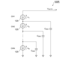
試験装置用の電源装置の最高出力電圧が、負荷に供給すべき高電圧に満たない場合、複数のチャンネルの電源装置(以下、電源ユニットと称する)を直列接続(以下、スタック接続)する必要がある。 If the maximum output voltage of the power supply for the test equipment is not sufficient to supply the high voltage to the load, it is necessary to connect multiple channels of power supplies (hereafter referred to as power supply units) in series (hereafter referred to as stack connection).
図1は、高電圧電源100Rのブロック図である。図1を参照すると、高電圧電源100Rは、スタック接続された複数チャンネルCH1~CHNの電源ユニット110_1~110_Nを備える。各チャンネルの電源ユニット110は、一次側Pと二次側Sを有し、一次側Pと二次側Sは、トランスやキャパシタなどのアイソレーションバリア112を介して絶縁されている。複数の電源ユニット110_1~110_Nの一次側Pの接地端子GND同士は、共通に接続される。
Figure 1 is a block diagram of the high-
電源ユニット110の二次側Sには、正極出力OUTPと負極出力OUTNが設けられ、正極出力OUTPと負極出力OUTNの間には、出力段120が設けられる。図1の構成では、全チャンネルが独立に動作し、i番目(i=1~N)のチャンネルの出力段120は、自身の出力電圧Viが目標値VREFに近づくように定電圧制御される。
A positive output OUTP and a negative output OUTN are provided on the secondary side S of the power supply unit 110, and an
i番目(1≦i≦N-1)のチャンネルの電源ユニット110_iの負極出力OUTNは、i+1番目のチャンネルの電源ユニット110_(i+1)の正極出力OUTPと接続される。1番目のチャンネルの電源ユニット110_1の正極出力OUTPは負荷1と接続され、N番目のチャンネルの電源ユニット110の負極出力OUTNは接地される。
The negative output OUTN of the power supply unit 110_i of the i-th (1≦i≦N-1) channel is connected to the positive output OUTP of the power supply unit 110_(i+1) of the i+1-th channel. The positive output OUTP of the power supply unit 110_1 of the 1st channel is connected to the
負荷1の両端間に供給される高電圧VOUTHは、各チャンネルの出力段120の発生電圧V1~VNの和であり、以下の式で表される。
VOUTH=Σ1:NVi
V1~VNそれぞれがVREFに安定化される定常状態では、出力電圧VOUTHは、N×VREFとなる。
The high voltage V OUTH supplied across the
VOUTH = Σ1: NVi
In a steady state where each of V 1 to V N is stabilized at V REF , the output voltage V OUTH is N×V REF .
複数のチャンネルの電源ユニットをスタック接続する場合の問題を説明する。図2(a)は、高電圧電源の出力電圧の波形図(シミュレーション結果)であり、図2(b)は、スタック段数Nとセトリング時間の関係を示す図である。なお、電圧波形は、セトリング後の電圧レベルで除算して正規化している。"simulation"は、図2(a)の波形から得られるスタック段数Nとセトリング時間の関係を示しており、スタック段数Nを増やすほど、セトリング時間が長くなってしまう。一方で、"expectation"で示すように、セトリング時間はスタック段数Nに係わらず一定であることが望まれる。 We will explain the problems that occur when power supply units of multiple channels are connected in a stack. Figure 2(a) is a waveform diagram (simulation result) of the output voltage of a high-voltage power supply, and Figure 2(b) is a diagram showing the relationship between the number of stack stages N and the settling time. Note that the voltage waveform is normalized by dividing it by the voltage level after settling. "Simulation" shows the relationship between the number of stack stages N and the settling time obtained from the waveform in Figure 2(a), and the more the number of stack stages N is increased, the longer the settling time becomes. On the other hand, as shown in "expectation", it is desirable for the settling time to be constant regardless of the number of stack stages N.
本開示の一態様は係る状況においてなされたものであり、その例示的な目的のひとつは、セトリング時間を短縮した高電圧電源の提供にある。 One aspect of the present disclosure has been made in this context, and one of its exemplary objectives is to provide a high-voltage power supply with reduced settling time.
本開示のある態様の電源装置は、スタック接続される複数チャンネルの電源ユニットを備える。複数チャンネルの電源ユニットはそれぞれ、正極出力および負極出力と、制御信号に応じて、正極出力と負極出力の間に出力電圧を発生する出力段と、出力電圧を示す電圧検出信号を生成する電圧検出器と、を備える。複数チャンネルのひとつであるマスターチャンネルの電源ユニットは、複数チャンネルの残りであるスレーブチャンネルの電源ユニットから電圧検出信号を受信し、全チャンネルの電圧検出信号にもとづくフィードバック信号を生成するフィードバック信号生成部と、フィードバック信号が目標値に近づくように、制御信号を生成するフィードバックコントローラと、をさらに備える。全チャンネルの出力段は、マスターチャンネルのフィードバックコントローラが生成する制御信号にもとづいて動作する。 A power supply device according to one embodiment of the present disclosure includes power supply units of multiple channels connected in a stack. Each of the power supply units of the multiple channels includes a positive output and a negative output, an output stage that generates an output voltage between the positive output and the negative output in response to a control signal, and a voltage detector that generates a voltage detection signal indicative of the output voltage. The power supply unit of a master channel, which is one of the multiple channels, further includes a feedback signal generating unit that receives a voltage detection signal from the power supply unit of a slave channel, which is the remaining channel, and generates a feedback signal based on the voltage detection signals of all the channels, and a feedback controller that generates a control signal so that the feedback signal approaches a target value. The output stages of all the channels operate based on the control signal generated by the feedback controller of the master channel.
本開示のある態様は、電源ユニットである。この電源ユニットは、複数個をスタックして電源装置を構成可能である。電源ユニットは、正極出力および負極出力と、制御信号に応じて、正極出力と負極出力の間に出力電圧を発生する出力段と、出力電圧を示す電圧検出信号を生成する電圧検出器と、マスターチャンネルに設定されたときにアクティブとなり、全チャンネルの電圧検出信号にもとづくフィードバック信号を生成するフィードバック信号生成部と、マスターチャンネルに設定されたときにアクティブとなり、フィードバック信号が目標値に近づくように、制御信号を生成するフィードバックコントローラと、マスターチャンネルに設定されたとき、他のチャンネルから電圧検出信号を受信するとともに、他のチャンネルに制御信号を送信し、スレーブチャンネルに設定されたとき、マスターチャンネルから制御信号を受信するとともに、マスターチャンネルに電圧検出信号を送信するインタフェース回路と、を備える。 One aspect of the present disclosure is a power supply unit. A power supply device can be configured by stacking a plurality of such power supply units. The power supply unit includes a positive output and a negative output, an output stage that generates an output voltage between the positive output and the negative output in response to a control signal, a voltage detector that generates a voltage detection signal indicating the output voltage, a feedback signal generating unit that becomes active when set to the master channel and generates a feedback signal based on the voltage detection signals of all channels, a feedback controller that becomes active when set to the master channel and generates a control signal so that the feedback signal approaches a target value, and an interface circuit that, when set to the master channel, receives a voltage detection signal from the other channels and transmits a control signal to the other channels, and, when set to the slave channel, receives a control signal from the master channel and transmits a voltage detection signal to the master channel.
なお、以上の構成要素の任意の組み合わせや、本発明の構成要素や表現を、方法、装置、システムなどの間で相互に置換したものもまた、本発明の態様として有効である。 In addition, any combination of the above components, or mutual substitution of the components or expressions of the present invention between methods, devices, systems, etc., are also valid aspects of the present invention.
本開示のある態様によれば、スタック段数が多いときのセトリング時間を短縮できる。 According to one aspect of the present disclosure, it is possible to reduce the settling time when there are many stack stages.
(実施形態の概要)
本開示のいくつかの例示的な実施形態の概要を説明する。この概要は、後述する詳細な説明の前置きとして、実施形態の基本的な理解を目的として、1つまたは複数の実施形態のいくつかの概念を簡略化して説明するものであり、発明あるいは開示の広さを限定するものではない。またこの概要は、考えられるすべての実施形態の包括的な概要ではなく、実施形態の欠くべからざる構成要素を限定するものではない。便宜上、「一実施形態」は、本明細書に開示するひとつの実施形態(実施例や変形例)または複数の実施形態(実施例や変形例)を指すものとして用いる場合がある。
(Overview of the embodiment)
A summary of some exemplary embodiments of the present disclosure will be described. This summary is intended to provide a simplified summary of some concepts of one or more embodiments for a basic understanding of the embodiments as a prelude to the detailed description that follows, and is not intended to limit the scope of the invention or disclosure. Furthermore, this summary is not an exhaustive summary of all possible embodiments, and is not intended to limit essential components of the embodiments. For convenience, the term "one embodiment" may be used to refer to one embodiment (example or variant) or multiple embodiments (examples or variants) disclosed in this specification.
はじめに、スタック段数Nが大きいほど、セトリング時間が長くなる理由について、本発明らが考察した結果を説明する。 First, we will explain the findings of the inventors regarding why the settling time increases as the number of stack stages N increases.
図3は、図1の高電圧電源100Rの等価回路図である。図1に示すように、各チャンネルの電源ユニット110は、一次側Pの接地端子GNDと二次側Sの負極出力OUTNの間に、アイソレーション容量CISOが存在する。図3に示すように、アイソレーション容量CISOは、出力段120から静電容量負荷として見え、スタックの段数(チャンネル数)Nが増えるほど、静電容量負荷が大きくなる。
Fig. 3 is an equivalent circuit diagram of the high
チャンネルごとに、静電容量負荷の大きさが異なるため、セトリング性能は、チャンネルごとにばらつくこととなる。このセトリング性能のばらつきが、高電圧電源100Rの出力電圧VOUTHのセトリング時間が長くなる原因のひとつとなる。
Since the capacitance load differs for each channel, the settling performance varies for each channel. This variation in settling performance is one of the causes of the long settling time of the output voltage VOUTH of the high
加えて、電源ユニット110(出力段120)には、電流クランプ機能(過電流保護機能)が実装される場合が多い。具体的には、電源ユニット110の出力段120は、その出力電流が所定のリミット値より低い状態では、定電圧制御が有効であるが、出力電流がリミット値を超えると、定電圧制御が無効となり、出力電流がリミット値に制限される(電流クランプ制御あるいは定電流制御ともいう)。
In addition, the power supply unit 110 (output stage 120) often has a current clamp function (overcurrent protection function) implemented. Specifically, when the output current of the
静電容量負荷が存在する状態で電圧印加を行うと、静電容量負荷に対して突入電流が流れ込む。各出力段120の出力電流は、負荷に流れる負荷電流と、突入電流の合計であるところ、突入電流の大きさは、チャンネルごとに異なる場合がある。すなわち1段目のチャンネルではアイソレーション容量CISOが見えないため、突入電流が発生しにくいのに対して、2段目以降のチャンネルでは、静電容量CISOが見えるため、突入電流が発生しやすい。
When a voltage is applied in the presence of a capacitive load, an inrush current flows into the capacitive load. The output current of each
一部のチャンネルで大きな突入電流が発生すると、そのチャンネルの出力段120の動作モードが、定電圧制御から電流クランプ制御に移行する。電流クランプ制御と定電圧制御が併存すると、図2(a)に示したように、高電圧電源100Rの出力電圧VOUTHに変曲点が現れて波形が歪む。そしてスタック段数が増えるほど、充電すべき静電容量が増えるため、出力電圧VOUTHが上昇する傾きは小さくなるため、セトリング時間が長くなる。
When a large inrush current occurs in a certain channel, the operation mode of the
以下では、セトリング時間の増加を抑制するための技術を説明する。 Below, we explain techniques for suppressing the increase in settling time.
一実施形態に係る電源装置は、スタック接続される複数チャンネルの電源ユニットを備える。複数チャンネルの電源ユニットはそれぞれ、正極出力および負極出力と、制御信号に応じて、正極出力と負極出力の間に出力電圧を発生する出力段と、出力電圧を示す電圧検出信号を生成する電圧検出器と、を備える。複数チャンネルのひとつであるマスターチャンネルの電源ユニットは、複数チャンネルの残りであるスレーブチャンネルの電源ユニットから電圧検出信号を受信し、全チャンネルの電圧検出信号にもとづくフィードバック信号を生成するフィードバック信号生成部と、フィードバック信号が目標値に近づくように、制御信号を生成するフィードバックコントローラと、をさらに備える。全チャンネルの出力段は、マスターチャンネルのフィードバックコントローラが生成する制御信号にもとづいて動作する。 A power supply device according to one embodiment includes power supply units for multiple channels that are stacked together. Each of the power supply units for the multiple channels includes a positive output and a negative output, an output stage that generates an output voltage between the positive output and the negative output in response to a control signal, and a voltage detector that generates a voltage detection signal that indicates the output voltage. The power supply unit for a master channel, which is one of the multiple channels, further includes a feedback signal generator that receives a voltage detection signal from a power supply unit for a slave channel, which is the remaining channel, and generates a feedback signal based on the voltage detection signals of all the channels, and a feedback controller that generates a control signal so that the feedback signal approaches a target value. The output stages for all the channels operate based on the control signal generated by the feedback controller for the master channel.
この構成によると、複数チャンネルの電源ユニットの出力段が、同じ制御信号にもとづいて動作する。そのため、チャンネルごとのセトリング性能のばらつきを解消することができ、これにより、チャンネル数を増やしたときにセトリング時間が増加するのを抑制できる。 With this configuration, the output stages of the power supply units for multiple channels operate based on the same control signal. This eliminates the variation in settling performance between channels, thereby preventing the settling time from increasing when the number of channels is increased.
一実施形態において、マスターチャンネルの電源ユニットは、出力段の出力電流を示す電流検出信号を生成する電流検出器をさらに備えてもよい。フィードバックコントローラは、電流検出信号が所定のリミット値を超えるとき、電流検出信号がリミット値に近づくように、制御信号を生成してもよい。 In one embodiment, the power supply unit of the master channel may further include a current detector that generates a current detection signal indicative of the output current of the output stage. When the current detection signal exceeds a predetermined limit value, the feedback controller may generate a control signal such that the current detection signal approaches the limit value.
電流クランプ制御は、マスターチャンネルが主導して全チャンネルで一斉に有効となる。したがって、電流クランプ制御と定電圧制御との混在を防止でき、セトリング時間が長くなるのを抑制できる。 The master channel takes the lead in controlling the current clamp control, which is enabled simultaneously for all channels. This prevents current clamp control and constant voltage control from being mixed together, and suppresses long settling times.
複数チャンネルの電源ユニットはそれぞれ、フィードバック信号生成部とフィードバックコントローラを備え、同様に構成されてもよい。各電源ユニットは、マスターモードとスレーブモードが選択可能であり、マスターモードに設定されたとき、フィードバック信号生成部とフィードバックコントローラが有効化され、スレーブモードに設定されたとき、フィードバック信号生成部とフィードバックコントローラが無効化されてもよい。なお、「ある回路ブロックを無効化する」ことは、当該ブロックを動作させない場合のみでなく、動作はさせるが、その出力を遮断あるいはマスクするなどして使用しない場合も含みうる。 The power supply units of the multiple channels may each have a feedback signal generating unit and a feedback controller and may be configured similarly. Each power supply unit may be able to select between master mode and slave mode, and when set to master mode, the feedback signal generating unit and the feedback controller may be enabled, and when set to slave mode, the feedback signal generating unit and the feedback controller may be disabled. Note that "disabling a certain circuit block" does not only mean that the block is not operated, but may also include a case where the block is operated but its output is blocked or masked so that it is not used.
同じ電源ユニットを複数用意し、接続関係を組み替えて、モードを適切に設定することにより、負荷の個数を変化させたりすることが可能となる。たとえばN個の電源ユニットがある場合に、N個をスタックしてそのうちのひとつをマスターモード、残りをスレーブモードとすれば、1個の負荷に対して電力を供給できる。あるいは、N個すべてをマスターモードとして独立に使用すれば、N個の負荷に対して電力を供給できる。 By preparing multiple identical power supply units, rearranging the connections, and setting the mode appropriately, it is possible to change the number of loads. For example, if there are N power supply units, you can stack them and set one to master mode and the rest to slave mode to supply power to one load. Alternatively, you can use all N units independently in master mode to supply power to N loads.
フィードバック信号は、全チャンネルの電圧検出信号の平均値であってもよい。これにより、全チャンネルの出力段や電圧検出器の特性のばらつきを加味して、正確な電圧を生成できる。 The feedback signal may be the average value of the voltage detection signals of all channels. This allows an accurate voltage to be generated taking into account the variations in the characteristics of the output stages and voltage detectors of all channels.
マスターチャンネルは、複数チャンネルのうち最上段に位置してもよい。突入電流がもっとも少ない最上段をマスターチャンネルとすることにより、電流クランプがかかりにくくなり、セトリング時間を短くできる。 The master channel may be located at the top of the multiple channels. By making the top channel, which has the least inrush current, the master channel, current clamping is less likely to occur, and the settling time can be shortened.
一実施形態に係る電源ユニットは、複数個をスタックして電源装置を構成可能である。電源ユニットは、正極出力および負極出力と、制御信号に応じて、正極出力と負極出力の間に出力電圧を発生する出力段と、出力電圧を示す電圧検出信号を生成する電圧検出器と、マスターチャンネルに設定されたときにアクティブとなり、全チャンネルの電圧検出信号にもとづくフィードバック信号を生成するフィードバック信号生成部と、マスターチャンネルに設定されたときにアクティブとなり、フィードバック信号が目標値に近づくように、制御信号を生成するフィードバックコントローラと、マスターチャンネルに設定されたとき、他のチャンネルから電圧検出信号を受信するとともに、他のチャンネルに制御信号を送信し、スレーブチャンネルに設定されたとき、マスターチャンネルから制御信号を受信するとともに、マスターチャンネルに電圧検出信号を送信するインタフェース回路と、を備える。 A power supply device can be configured by stacking a plurality of power supply units according to one embodiment. The power supply unit includes a positive output and a negative output, an output stage that generates an output voltage between the positive output and the negative output in response to a control signal, a voltage detector that generates a voltage detection signal indicating the output voltage, a feedback signal generating section that becomes active when set to the master channel and generates a feedback signal based on the voltage detection signals of all channels, a feedback controller that becomes active when set to the master channel and generates a control signal so that the feedback signal approaches a target value, and an interface circuit that receives voltage detection signals from other channels and transmits control signals to other channels when set to the master channel, and receives control signals from the master channel and transmits voltage detection signals to the master channel when set to the slave channel.
この構成によると、複数チャンネルをスタックした場合に、すべての電源ユニットの出力段が、同じ制御信号にもとづいて動作する。そのため、チャンネルごとのセトリング性能のばらつきを解消することができ、これにより、チャンネル数を増やしたときにセトリング時間が増加するのを抑制できる。また、同じ電源ユニットを複数用意し、接続関係を組み替えて、モードを適切に設定することにより、負荷の個数を変化させたりすることが可能となる。 With this configuration, when multiple channels are stacked, the output stages of all power supply units operate based on the same control signal. This eliminates the variation in settling performance between channels, which makes it possible to prevent the settling time from increasing when the number of channels is increased. In addition, by preparing multiple identical power supply units, rearranging the connections, and appropriately setting the mode, it is possible to change the number of loads.
(実施形態)
以下、本発明を好適な実施の形態をもとに図面を参照しながら説明する。各図面に示される同一または同等の構成要素、部材、処理には、同一の符号を付するものとし、適宜重複した説明は省略する。また、実施の形態は、発明を限定するものではなく例示であって、実施の形態に記述されるすべての特徴やその組み合わせは、必ずしも発明の本質的なものであるとは限らない。
(Embodiment)
The present invention will be described below based on preferred embodiments with reference to the drawings. The same or equivalent components, parts, and processes shown in each drawing are given the same reference numerals, and duplicated descriptions are omitted as appropriate. In addition, the embodiments are illustrative rather than limiting the invention, and all features and combinations thereof described in the embodiments are not necessarily essential to the invention.
本明細書において、「部材Aが、部材Bと接続された状態」とは、部材Aと部材Bが物理的に直接的に接続される場合のほか、部材Aと部材Bが、それらの電気的な接続状態に実質的な影響を及ぼさない、あるいはそれらの結合により奏される機能や効果を損なわせない、その他の部材を介して間接的に接続される場合も含む。 In this specification, "a state in which component A is connected to component B" includes not only cases in which component A and component B are directly physically connected, but also cases in which component A and component B are indirectly connected via other components that do not substantially affect their electrical connection state or impair the function or effect achieved by their combination.
同様に、「部材Cが、部材Aと部材Bの間に設けられた状態」とは、部材Aと部材C、あるいは部材Bと部材Cが直接的に接続される場合のほか、それらの電気的な接続状態に実質的な影響を及ぼさない、あるいはそれらの結合により奏される機能や効果を損なわせない、その他の部材を介して間接的に接続される場合も含む。 Similarly, "a state in which component C is provided between components A and B" includes not only cases in which components A and C, or components B and C, are directly connected, but also cases in which they are indirectly connected via other components that do not substantially affect their electrical connection state or impair the function or effect achieved by their combination.
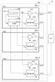
図4は、実施の形態に係る電源装置100を備える試験装置2を示すブロック図である。試験装置2は、DUT(被試験デバイス)1に電圧信号や電流信号などの試験信号を印加し、DUT1の応答を測定する。DUT1の種類は特に限定されないが、高耐圧パワートランジスタやパワーモジュールなどの1000Vを超えるような高電圧の電圧印加を必要とするデバイス、あるいはそうしたデバイスを含む回路、もしくは回路システムが、本試験装置2の試験対象として好適である。
Figure 4 is a block diagram showing a
試験装置2は、DUT1に電源信号を供給する電源装置100を備える。電源信号は、典型的には、所定の電圧レベルに安定化された電圧信号VOUTHである。なお、図4では、DUT1に直接、電源信号VOUTHが供給されているが、その限りでなく、この電源信号VOUTHは、DUT1の周辺回路や、DUT1を駆動する回路、DUT1とのインタフェースとなる回路に供給されてもよい。
The
試験装置2は、電源装置100に加えて、電圧センサや電流センサ、信号発生器やドライバ、コンパレータ、A/Dコンバータ、D/Aコンバータなどを備えるが、それらはDUT1の種類や試験項目に応じており、図4では省略している。
In addition to the
電源装置100は、スタック接続される複数Nチャンネル(CH1~CHN)の電源ユニット200_1~200_Nを備える。各電源ユニット200は、正極出力OUTPと負極出力OUTNを有している。電源ユニット200は、図1の電源ユニット110と同様に、絶縁された1次側と2次側を有しているが、図4には二次側の構成のみを示す。負極出力OUTNは、二次側の基準電位(グランド)をなす。
The
i番目(1≦i≦N-1)のチャンネルの電源ユニット110_iの負極出力OUTNは、i+1番目のチャンネルの電源ユニット110_(i+1)の正極出力OUTPと接続される。1番目のチャンネルの電源ユニット110_1の正極出力OUTPは負荷1と接続され、N番目のチャンネルの電源ユニット110の負極出力OUTNは接地される。
The negative output OUTN of the power supply unit 110_i of the i-th (1≦i≦N-1) channel is connected to the positive output OUTP of the power supply unit 110_(i+1) of the i+1-th channel. The positive output OUTP of the power supply unit 110_1 of the 1st channel is connected to the
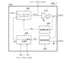
複数チャンネルの電源ユニット200はそれぞれ、出力段210、電圧検出器220を備える。i番目(i=1~N)の電源ユニット200_iの出力段210は、制御信号Vctrlに応じて、正極出力OUTPと負極出力OUTNの間に出力電圧Viを発生する。またi番目の電源ユニット200_iの電圧検出器220は、対応する出力電圧Viを示す電圧検出信号Vsiを生成する。
Each of the
本実施形態において、複数NチャンネルCH1~CHNは、ひとつがマスターチャンネルに、残りがスレーブチャンネルに設定される。その限りでないが、図4では1番目のチャンネルCH1がマスターチャンネルであり、2番目~N番目のチャンネルCH2~CHNがスレーブチャンネルである。 In this embodiment, of the multiple N channels CH1 to CHN, one is set as the master channel and the rest are set as slave channels. Although not limited to this, in FIG. 4, the first channel CH1 is the master channel and the second to Nth channels CH2 to CHN are slave channels.
マスターチャンネルとスレーブチャンネルとの間は、信号の送受信が可能となっている。スレーブチャンネルの電源ユニット200_2~200_Nは、電圧検出信号Vs1~VsNを、マスターチャンネルの電源ユニット200_1に送信する。 Signals can be transmitted and received between the master channel and the slave channel. The power supply units 200_2 to 200_N of the slave channels transmit voltage detection signals Vs 1 to Vs N to the power supply unit 200_1 of the master channel.
マスターチャンネルの電源ユニット200_1は、出力段210および電圧検出器220に加えて、フィードバック信号生成部230およびフィードバックコントローラ240を備える。
The power supply unit 200_1 of the master channel includes an
フィードバック信号生成部230は、スレーブチャンネルの電源ユニット200_2~200_Nから電圧検出信号Vs2~VsNを受信し、全チャンネルCH1~CHNの電圧検出信号Vs1~VsNにもとづくフィードバック信号Vfbを生成する。たとえばフィードバック信号Vfbは、複数の電圧検出信号Vs1~VsNの単純平均値であってもよい。なお、フィードバック信号Vfbはそれに限定されない。
The feedback
たとえば複数のチャンネルの電源ユニット200_1~200_Nにバラツキが存在する場合、バラツキを考慮した係数を利用して、重み付け平均を取ってもよい。 For example, if there is variation in the power supply units 200_1 to 200_N of multiple channels, a weighted average may be calculated using a coefficient that takes the variation into account.
フィードバックコントローラ240には、目標値Vrefが入力される。フィードバックコントローラ240は、フィードバック信号Vfbが目標値Vrefに近づくように、制御信号Vctrlの信号レベル(大きさ)をフィードバック制御する。
The target value Vref is input to the
フィードバックコントローラ240が生成した制御信号Vctrlは、マスターチャンネルの出力段210に供給される。さらにこの制御信号Vctrlは、マスターチャンネルの電源ユニット200_1から、スレーブチャンネルの電源ユニット200_2~200_Nに伝送される。そして全チャンネルCH1~CHNの出力段210は、マスターチャンネルCH1のフィードバックコントローラ240が生成する制御信号Vctrlにもとづいて動作する。
The control signal Vctrl generated by the
以上が電源装置100の基本構成である。
The above is the basic configuration of the
この構成によると、複数チャンネルCH1~CHNの電源ユニット200_1~200_Nの出力段210が、同じ制御信号Vctrlにもとづいて動作する。そのため、チャンネルごとのセトリング性能のばらつきを解消することができ、これにより、チャンネル数Nを増やしたときにセトリング時間が増加するのを抑制できる。 With this configuration, the output stages 210 of the power supply units 200_1 to 200_N of the multiple channels CH1 to CHN operate based on the same control signal Vctrl. This eliminates the variation in settling performance between channels, thereby preventing the settling time from increasing when the number of channels N is increased.
本開示は、図4のブロック図や回路図として把握され、あるいは上述の説明から導かれるさまざまな装置、方法に及ぶものであり、特定の構成に限定されるものではない。以下、本発明の範囲を狭めるためではなく、発明の本質や動作の理解を助け、またそれらを明確化するために、より具体的な構成例や実施例を説明する。 This disclosure covers various devices and methods that can be understood as the block diagram or circuit diagram of FIG. 4 or derived from the above description, and is not limited to any particular configuration. Below, more specific configuration examples and examples are described, not to narrow the scope of the present invention, but to aid in understanding and clarify the essence and operation of the invention.
(実施例1)
図5は、実施例1に係るマスターチャンネルの電源ユニット200_1の構成例を示すブロック図である。この電源ユニット200_1は電流クランプ機能を有する。具体的には電源ユニット200_1は、図4の電源ユニット200_1に加えて、電流検出器250を備える。電流検出器250は、出力段210の出力電流IOUTを示す電流検出信号Is1を生成する。この電流検出信号Is1は、フィードバックコントローラ240に入力される。
Example 1
5 is a block diagram showing a configuration example of a power supply unit 200_1 of the master channel according to the first embodiment. This power supply unit 200_1 has a current clamp function. Specifically, the power supply unit 200_1 includes a
フィードバックコントローラ240は、電流検出信号Is1が所定のリミット値より低い状態では、上述のように、フィードバック信号Vfbが目標値Vrefに近づくように、制御信号Vctrlを生成する(定電圧制御)。一方、電流検出信号Is1がリミット値を超えた状態では、定電圧制御が無効となり、電流検出信号Is1がリミット値に近づくように、制御信号Vctrlを生成する(電流クランプ制御)。
When the current detection signal Is1 is lower than a predetermined limit value, the
電流クランプ機能に関するハードウェアはマスターチャンネルにのみ設けられ、あるいは、後述のように、設けられる場合であっても、スレーブチャンネルにおいて当該ハードウェアは無効化される。 Hardware for the current clamp function is provided only in the master channel, or, if provided, the hardware is disabled in the slave channels, as described below.
マスターチャンネルにおいて電流検出信号Is1がリミット値を超えると、電流クランプ制御のための制御信号Vctrlが生成され、これによって、全チャンネルの出力段210が動作する。つまり電流クランプ制御は、マスターチャンネルが主導して全チャンネルで一斉に有効となる。したがって、図1の構成において生じていた、電流クランプ制御と定電圧制御との混在を防止でき、セトリング時間が長くなるのを抑制できる。 When the current detection signal Is1 in the master channel exceeds the limit value, a control signal Vctrl for current clamp control is generated, which operates the output stages 210 of all channels. In other words, the current clamp control is enabled simultaneously in all channels under the initiative of the master channel. This makes it possible to prevent the current clamp control and the constant voltage control from being mixed together, as occurred in the configuration of FIG. 1, and to suppress the settling time from becoming long.
なお、図3を参照して説明したように、複数チャンネルをスタックする場合、最も高電位側のチャンネルが、アイソレーション容量CISOの影響を受けにくく、したがって突入電流が発生しにくいといえる。したがって、マスターチャンネルに電流クランプ機能を実装する場合、突入電流が発生しにくい最上段のチャンネルをマスターチャンネルとすることで、電流クランプがかかりにくくなるため、セトリング時間をさらに短縮できる。 As described with reference to Fig. 3, when multiple channels are stacked, the channel with the highest potential is less susceptible to the isolation capacitance CISO and therefore is less likely to generate inrush current. Therefore, when implementing a current clamp function in the master channel, by making the topmost channel, which is less likely to generate inrush current, the current clamp is less likely to be applied as the master channel, and the settling time can be further shortened.
(実施例2)
マスターチャンネルの電源ユニット200と、スレーブチャンネルの電源ユニット200は、はじめから別々の構成として設計しておいてもよいが、以下で説明するように、同じ構成として、マスターチャンネルとして動作させるときのモードと、スレーブチャンネルとして動作させるときのモードを、切りかえ可能に構成してもよい。
Example 2
The
図6は、実施例2に係る電源ユニット200のブロック図である。この電源ユニット200は、マスターチャンネル、スレーブチャンネルの両方で使用可能である。電源ユニット200は、モードセレクタ260、マルチプレクサ(スイッチ)270を備える。
FIG. 6 is a block diagram of a
モードセレクタ260は、マスターチャンネルで使用されるときマスターモード、スレーブチャンネルで使用されるときスレーブモードであることを示すモード制御信号MODEを生成する。モード制御信号MODEは、フィードバック信号生成部230、フィードバックコントローラ240、電流検出器250のイネーブル端子に入力され、これらのブロックは、モード制御信号MODEがマスターモードを示すときにイネーブル、スレーブモードを示すときにディセーブルとなる。
The
マルチプレクサ270のひとつの入力ノードには、同じ電源ユニット200内のフィードバックコントローラ240の出力が接続される。またマルチプレクサ270の別の入力ノードには、別の電源ユニット200において生成された制御信号Vctrlが入力可能となっている。マルチプレクサ270は、モード制御信号MODEがマスターモードを示すときに、同じ電源ユニット200内の制御信号(内部制御信号)Vctrl_intを選択し、スレーブモードを示すときに他の電源ユニット200で生成された外部からの制御信号Vctrl_extを選択する。
One input node of the
また電源ユニット200は、その内部で生成した制御信号Vctrl_int、電圧検出信号Vsiは、外部に出力可能となっている。また電源ユニット200は、外部で生成された制御信号Vctrl_ext、電圧検出信号Vsiを受信可能となっている。
The
図7(a)、(b)は、マスターモード、スレーブモードにおける図6の電源ユニット200の状態を示す図である。図7(a)、(b)において、ディセーブルとなるブロックや信号線は一点鎖線で示す。
Figures 7(a) and (b) are diagrams showing the states of the
図8は、電源ユニット200の具体的な構成例を示すブロック図である。この電源ユニット200は、その制御系がデジタル回路のアーキテクチャで実装され、検出信号や制御信号はデジタル信号である。
Figure 8 is a block diagram showing a specific example configuration of the
出力段210は、D/Aコンバータ212およびパワーアンプ214を含む。出力段210は、入力されたデジタルの制御信号Vctrlをアナログの制御信号に変換する。パワーアンプ214は、アナログの制御信号を増幅し、正極出力OUTPに出力する。
The
電圧検出器220は、電圧センスアンプ222とA/Dコンバータ224を含む。電圧センスアンプ222は、2つの出力OUTPTとOUTN間の電圧Viを増幅する。A/Dコンバータ224は、センスアンプ222の出力をデジタルの電圧検出信号Vsiに変換する。電圧検出信号Vsiはインタフェース回路280を介して他のチャンネルと共有可能となっている。
The
フィードバック信号生成部230は、加減算器232および除算器234を含む。加減算器232は、同じチャンネルおよび他のチャンネルの電圧検出信号Vsiを加算する。除算器234は、加減算器232の出力を、チャンネル数Nで除算し、平均値にもとづくフィードバック信号Vfbを生成する。除算器234は、加減算器232の出力に係数1/Nを乗算する係数回路とも把握できる。
The feedback
電流検出器250は、センス抵抗252、センスアンプ254、A/Dコンバータ256を含む。センス抵抗252は、出力段210の出力電流IOUTの経路上に設けられる。センス抵抗252には、出力電流IOUTに比例した電圧降下が発生する。センスアンプ254は、センス抵抗252の電圧降下を増幅する。A/Dコンバータ256は、センスアンプ254の出力をデジタルの電流検出信号Isiに変換する。フィードバックコントローラ240には、電圧の目標値Vrefと、電流のリミット値Ilimが入力される。
The
加減算器242は、目標値Vrefとフィードバック信号Vfbの差分(電圧誤差Verr)を生成する。加減算器246は、リミット値Ilimと電流検出信号Isiの差分(電流誤差Ierr)を生成する。
The adder-
セレクタ248は、Isi<Ilimのときに、電圧誤差Verrを選択し(定電圧制御)、Isi>Ilimのときに、電流誤差Ierrを選択する(電流クランプ制御)。
The
フィルタ244は、セレクタ248の出力にもとづいて、制御信号Vctrlを生成する。その限りでないが、フィルタ244は、PI(比例積分)制御器やPID(比例積分微分)制御器などで構成することができる。定電圧制御では、電圧誤差Verrがゼロに近づくように、制御信号Vctrlのレベルがフィードバックにより調節され、電流クランプ制御では、電流誤差Ierrがゼロに近づくように、制御信号Vctrlのレベルがフィードバックにより調節される。フィルタ244のパラメータは、定電圧制御と電流クランプ制御とで切りかえてもよい。
The
フィードバックコントローラ240およびフィードバック信号生成部230は、CPU(Central Processing Unit)、DSP(Digital Signal Processor)またはFPGA(Field Programmable Gate Array)などで構成することができる。
The
インタフェース回路280は、他のチャンネルのインタフェース回路280との間で、電圧検出信号や制御信号Vctrlを送受信可能である。
The
図9は、図8の電源ユニット200を2個組み合わせた電源装置の動作波形図である。実施形態に係る電源装置と従来の電源装置それぞれの波形が示される。1段1000V出力の電源ユニットが2チャンネルスタックされており、出力電圧は2000Vである。従来方式の波形(ii)では、電圧印加直後の立ち上がりが速いが、1000Vを超えたあたりからの上昇が緩やかとなっている。これは上段のチャンネルは電圧印加制御のセトリング波形となる一方で、下段のチャンネルが静電容量への突入電流による電流クランプ制御となりセトリング時間の増加を招いているためである。これに対して実施形態に係る波形(i)は、電圧印加制御で両者のチャンネルがバランスを取りながら動作するため、セトリング時間が短縮できていることが分かる。本実施形態によれば、2000Vへのセトリング時間を従来方式の12msから4msへと従来比1/3以下に短縮されていることが確認できた。
9 is an operating waveform diagram of a power supply device combining two
以上、本発明について、実施の形態をもとに説明した。この実施の形態は例示であり、それらの各構成要素や各処理プロセス、それらの組み合わせには、さまざまな変形例が存在しうる。以下、こうした変形例について説明する。 The present invention has been described above based on an embodiment. This embodiment is merely an example, and various modifications may be made to the components, processing processes, and combinations thereof. These modifications are described below.
図8では、その制御系がデジタル回路のアーキテクチャで実装される電源ユニット200について説明したが、その限りでなく、制御系をアナログ回路で構成してもよい。
In FIG. 8, a
電流クランプ機能について、マスターチャンネルにおいて出力電流を監視することとしたがその限りでない。たとえば、ひとつのスレーブチャンネルにおいて出力電流を監視し、スレーブチャンネルにおいて得られた電流検出値を、マスターチャンネルに送信してもよい。マスターチャンネルのフィードバックコントローラ240は、スレーブチャンネルの電流検出信号Isにもとづいて、電流クランプ制御をかけてもよい。
Although the current clamp function is described as monitoring the output current in the master channel, this is not limited to this. For example, the output current may be monitored in one slave channel, and the current detection value obtained in the slave channel may be transmitted to the master channel. The
あるいは全チャンネルの電流検出器を有効化し、スレーブチャンネルからマスターチャンネルに電流検出信号を送信するようにしてもよい。マスターチャンネルのフィードバックコントローラ240は、全チャンネルの電流検出信号の最大値が、リミット値Ilimを超えないように、電流クランプ制御をかけてもよい。
Alternatively, the current detectors of all channels may be enabled and a current detection signal may be sent from the slave channel to the master channel. The
実施の形態にもとづき本発明を説明したが、実施の形態は、本発明の原理、応用を示しているにすぎず、実施の形態には、請求の範囲に規定された本発明の思想を逸脱しない範囲において、多くの変形例や配置の変更が認められる。 The present invention has been described based on the embodiments, but the embodiments merely show the principles and applications of the present invention, and many modifications and changes in arrangement are permitted to the embodiments as long as they do not deviate from the concept of the present invention as defined in the claims.
1…DUT、2…試験装置、100…電源装置、200…電源ユニット、210…出力段、220…電圧検出器、230…フィードバック信号生成部、240…フィードバックコントローラ、250…電流検出器、260…モードセレクタ、270…マルチプレクサ、280…インタフェース回路。 1...DUT, 2...test device, 100...power supply device, 200...power supply unit, 210...output stage, 220...voltage detector, 230...feedback signal generator, 240...feedback controller, 250...current detector, 260...mode selector, 270...multiplexer, 280...interface circuit.
Claims (10)
前記複数チャンネルの電源ユニットはそれぞれ、
正極出力および負極出力と、
制御信号に応じて、前記正極出力と前記負極出力の間に出力電圧を発生する出力段と、
前記出力電圧を示す電圧検出信号を生成する電圧検出器と、
を備え、
前記複数チャンネルのひとつであるマスターチャンネルの電源ユニットは、
前記複数チャンネルの残りであるスレーブチャンネルの電源ユニットから前記電圧検出信号を受信し、全チャンネルの前記電圧検出信号にもとづくフィードバック信号を生成するフィードバック信号生成部と、
前記フィードバック信号が目標値に近づくように、前記制御信号を生成するフィードバックコントローラと、
をさらに備え、
全チャンネルの前記出力段は、前記マスターチャンネルの前記フィードバックコントローラが生成する前記制御信号にもとづいて動作することを特徴とする電源装置。 Equipped with a multi-channel power supply unit that is stacked,
Each of the multiple channel power supply units comprises:
a positive output and a negative output;
an output stage for generating an output voltage between the positive output and the negative output in response to a control signal;
a voltage detector for generating a voltage detection signal indicative of the output voltage;
Equipped with
The power supply unit of the master channel, which is one of the multiple channels,
a feedback signal generating unit that receives the voltage detection signal from a power supply unit of a slave channel that is the remaining of the plurality of channels, and generates a feedback signal based on the voltage detection signals of all the channels;
a feedback controller for generating the control signal so that the feedback signal approaches a target value;
Further equipped with
A power supply device, characterized in that the output stages of all channels operate based on the control signal generated by the feedback controller of the master channel.
前記フィードバックコントローラは、前記電流検出信号が所定のリミット値を超えるとき、前記電流検出信号が前記リミット値に近づくように、前記制御信号を生成することを特徴とする請求項1に記載の電源装置。 the power supply unit of the master channel further comprises a current detector for generating a current detection signal indicative of an output current of the output stage;
2. The power supply device according to claim 1, wherein the feedback controller generates the control signal when the current detection signal exceeds a predetermined limit value so that the current detection signal approaches the limit value.
各電源ユニットは、マスターモードとスレーブモードが選択可能であり、前記マスターモードに設定されたとき、前記フィードバック信号生成部、前記フィードバックコントローラが有効化され、前記スレーブモードに設定されたとき、前記フィードバック信号生成部と前記フィードバックコントローラが無効化されることを特徴とする請求項2に記載の電源装置。 The multi-channel power supply unit is configured similarly to the feedback signal generator, the feedback controller, and the current detector;
3. The power supply device according to claim 2, wherein each power supply unit is selectable between a master mode and a slave mode, and when set to the master mode, the feedback signal generating unit and the feedback controller are enabled, and when set to the slave mode, the feedback signal generating unit and the feedback controller are disabled.
正極出力および負極出力と、
制御信号に応じて、前記正極出力と前記負極出力の間に出力電圧を発生する出力段と、
前記出力電圧を示す電圧検出信号を生成する電圧検出器と、
マスターチャンネルに設定されたときにアクティブとなり、全チャンネルの前記電圧検出信号にもとづくフィードバック信号を生成するフィードバック信号生成部と、
前記マスターチャンネルに設定されたときにアクティブとなり、前記フィードバック信号が目標値に近づくように、制御信号を生成するフィードバックコントローラと、
前記マスターチャンネルに設定されたとき、他のチャンネルから前記電圧検出信号を受信するとともに、他のチャンネルに前記制御信号を送信し、スレーブチャンネルに設定されたとき、前記マスターチャンネルから前記制御信号を受信するとともに、前記マスターチャンネルに前記電圧検出信号を送信するインタフェース回路と、
を備えることを特徴とする電源ユニット。 A power supply unit that can be stacked to form a power supply device,
a positive output and a negative output;
an output stage for generating an output voltage between the positive output and the negative output in response to a control signal;
a voltage detector for generating a voltage detection signal indicative of the output voltage;
a feedback signal generating unit which becomes active when the channel is set as a master channel and generates a feedback signal based on the voltage detection signals of all the channels;
a feedback controller that is active when the master channel is selected and generates a control signal so that the feedback signal approaches a target value;
an interface circuit which, when set as the master channel, receives the voltage detection signal from the other channels and transmits the control signal to the other channels, and, when set as the slave channel, receives the control signal from the master channel and transmits the voltage detection signal to the master channel;
A power supply unit comprising:
前記マスターチャンネルに設定されたとき、前記フィードバックコントローラは、前記電流検出信号が所定のリミット値を超えるとき、前記電流検出信号が前記リミット値に近づくように、前記制御信号を生成することを特徴とする請求項6に記載の電源ユニット。 a current detector for generating a current detection signal indicative of an output current of the output stage;
7. The power supply unit of claim 6, wherein when set to the master channel, the feedback controller generates the control signal when the current detection signal exceeds a predetermined limit value so that the current detection signal approaches the limit value.
Priority Applications (7)
| Application Number | Priority Date | Filing Date | Title |
|---|---|---|---|
| JP2020198413A JP7561589B2 (en) | 2020-11-30 | 2020-11-30 | Power supplies, power supply units, test equipment |
| DE112021006236.0T DE112021006236T5 (en) | 2020-11-30 | 2021-10-20 | POWER SUPPLY DEVICE, POWER SUPPLY UNIT AND TEST DEVICE |
| KR1020237008391A KR102766653B1 (en) | 2020-11-30 | 2021-10-20 | Power supply, power unit, test device |
| CN202180066119.7A CN116325464A (en) | 2020-11-30 | 2021-10-20 | Power supply unit, power supply unit, test device |
| PCT/JP2021/038779 WO2022113579A1 (en) | 2020-11-30 | 2021-10-20 | Power supply device, power supply unit, and test device |
| TW110139696A TWI788066B (en) | 2020-11-30 | 2021-10-26 | Power supply units, power supply units, test equipment |
| US18/312,000 US12388347B2 (en) | 2020-11-30 | 2023-05-04 | Power supply apparatus |
Applications Claiming Priority (1)
| Application Number | Priority Date | Filing Date | Title |
|---|---|---|---|
| JP2020198413A JP7561589B2 (en) | 2020-11-30 | 2020-11-30 | Power supplies, power supply units, test equipment |
Publications (2)
| Publication Number | Publication Date |
|---|---|
| JP2022086417A JP2022086417A (en) | 2022-06-09 |
| JP7561589B2 true JP7561589B2 (en) | 2024-10-04 |
Family
ID=81754322
Family Applications (1)
| Application Number | Title | Priority Date | Filing Date |
|---|---|---|---|
| JP2020198413A Active JP7561589B2 (en) | 2020-11-30 | 2020-11-30 | Power supplies, power supply units, test equipment |
Country Status (7)
| Country | Link |
|---|---|
| US (1) | US12388347B2 (en) |
| JP (1) | JP7561589B2 (en) |
| KR (1) | KR102766653B1 (en) |
| CN (1) | CN116325464A (en) |
| DE (1) | DE112021006236T5 (en) |
| TW (1) | TWI788066B (en) |
| WO (1) | WO2022113579A1 (en) |
Families Citing this family (1)
| Publication number | Priority date | Publication date | Assignee | Title |
|---|---|---|---|---|
| JP7634975B2 (en) * | 2020-11-30 | 2025-02-25 | 株式会社アドバンテスト | Power supplies, power supply units, test equipment |
Citations (6)
| Publication number | Priority date | Publication date | Assignee | Title |
|---|---|---|---|---|
| JP2002165441A (en) | 2000-11-20 | 2002-06-07 | Shibaura Mechatronics Corp | DC power supply |
| JP2003304688A (en) | 2002-04-10 | 2003-10-24 | Fujitsu Access Ltd | Direct-current power supply unit |
| JP2014147196A (en) | 2013-01-29 | 2014-08-14 | Myway Corp | Power-supply system and power-supply device |
| JP2016208742A (en) | 2015-04-24 | 2016-12-08 | 株式会社デンソー | Power converter |
| JP2017127195A (en) | 2013-10-02 | 2017-07-20 | 株式会社村田製作所 | Power supply system |
| US20200295563A1 (en) | 2017-12-07 | 2020-09-17 | Nr Electric Co., Ltd. | Voltage and current control method and device for direct-current power transmission system |
Family Cites Families (21)
| Publication number | Priority date | Publication date | Assignee | Title |
|---|---|---|---|---|
| JPS62221872A (en) * | 1986-03-24 | 1987-09-29 | Hitachi Ltd | power supply |
| US4766364A (en) * | 1987-11-04 | 1988-08-23 | International Business Machines Corporation | Parallel power systems |
| JP3333351B2 (en) * | 1995-04-13 | 2002-10-15 | 株式会社東芝 | Switching regulator |
| US7123493B2 (en) * | 2004-08-10 | 2006-10-17 | Advantest Corporation | Power source apparatus |
| US7151362B1 (en) | 2005-06-03 | 2006-12-19 | The Aerospace Corporation | Uniform converter output voltage distribution power system |
| US8618788B2 (en) * | 2007-03-30 | 2013-12-31 | Malay Trivedi | Dynamically adjusted multi-phase regulator |
| WO2011010388A1 (en) * | 2009-07-24 | 2011-01-27 | Necディスプレイソリューションズ株式会社 | Switching power source and electronic device using the same |
| US8946937B2 (en) * | 2010-08-18 | 2015-02-03 | Volterra Semiconductor Corporation | Switching circuits for extracting power from an electric power source and associated methods |
| GB201110823D0 (en) * | 2011-06-27 | 2011-08-10 | Cooper Technologies Co | Power supply |
| TWI429182B (en) * | 2011-08-12 | 2014-03-01 | Upi Semiconductor Corp | Multi-phase dc-dc converter |
| JP5802549B2 (en) | 2011-12-28 | 2015-10-28 | コーセル株式会社 | Power supply device and power supply system using the same |
| JP2015065738A (en) * | 2013-09-24 | 2015-04-09 | Tdk株式会社 | Power supply control circuit and power supply unit |
| CN105990999A (en) * | 2015-01-27 | 2016-10-05 | 台达电子工业股份有限公司 | Power supply device and control method thereof |
| JP6555471B2 (en) * | 2015-08-05 | 2019-08-07 | 富士電機株式会社 | Power conditioner for photovoltaic power generation and photovoltaic power generation system |
| KR101759619B1 (en) * | 2017-02-07 | 2017-07-20 | 엘아이지넥스원 주식회사 | Power supply apparatus including the dc to dc convertor and power supply method thereof |
| JP6926762B2 (en) | 2017-07-18 | 2021-08-25 | Tdk株式会社 | Power supply |
| JP7124297B2 (en) * | 2017-10-31 | 2022-08-24 | 富士電機株式会社 | power converter |
| CN108173260A (en) * | 2017-12-22 | 2018-06-15 | 固纬电子(苏州)有限公司 | Multichannel power source combination control system |
| CN111864722A (en) * | 2019-04-25 | 2020-10-30 | 康普技术有限责任公司 | Current sharing control circuit, power supply system and current sharing control method |
| CN109980926B (en) * | 2019-04-30 | 2024-05-14 | 苏州易美新思新能源科技有限公司 | Multichannel serial power supply |
| JP7658107B2 (en) * | 2021-02-18 | 2025-04-08 | マツダ株式会社 | Current detection circuit and load drive control device equipped with the same |
-
2020
- 2020-11-30 JP JP2020198413A patent/JP7561589B2/en active Active
-
2021
- 2021-10-20 WO PCT/JP2021/038779 patent/WO2022113579A1/en not_active Ceased
- 2021-10-20 DE DE112021006236.0T patent/DE112021006236T5/en active Pending
- 2021-10-20 KR KR1020237008391A patent/KR102766653B1/en active Active
- 2021-10-20 CN CN202180066119.7A patent/CN116325464A/en active Pending
- 2021-10-26 TW TW110139696A patent/TWI788066B/en active
-
2023
- 2023-05-04 US US18/312,000 patent/US12388347B2/en active Active
Patent Citations (6)
| Publication number | Priority date | Publication date | Assignee | Title |
|---|---|---|---|---|
| JP2002165441A (en) | 2000-11-20 | 2002-06-07 | Shibaura Mechatronics Corp | DC power supply |
| JP2003304688A (en) | 2002-04-10 | 2003-10-24 | Fujitsu Access Ltd | Direct-current power supply unit |
| JP2014147196A (en) | 2013-01-29 | 2014-08-14 | Myway Corp | Power-supply system and power-supply device |
| JP2017127195A (en) | 2013-10-02 | 2017-07-20 | 株式会社村田製作所 | Power supply system |
| JP2016208742A (en) | 2015-04-24 | 2016-12-08 | 株式会社デンソー | Power converter |
| US20200295563A1 (en) | 2017-12-07 | 2020-09-17 | Nr Electric Co., Ltd. | Voltage and current control method and device for direct-current power transmission system |
Also Published As
| Publication number | Publication date |
|---|---|
| DE112021006236T5 (en) | 2023-10-05 |
| US20230353055A1 (en) | 2023-11-02 |
| TW202223431A (en) | 2022-06-16 |
| TWI788066B (en) | 2022-12-21 |
| KR102766653B1 (en) | 2025-02-12 |
| CN116325464A (en) | 2023-06-23 |
| JP2022086417A (en) | 2022-06-09 |
| WO2022113579A1 (en) | 2022-06-02 |
| US12388347B2 (en) | 2025-08-12 |
| KR20230048415A (en) | 2023-04-11 |
Similar Documents
| Publication | Publication Date | Title |
|---|---|---|
| US9112419B2 (en) | AC/DC converter with control circuit that receives rectified voltage at input detection terminal | |
| US6900621B1 (en) | Digitally controlled modular power supply for automated test equipment | |
| CN105229908A (en) | Protection of Switched Capacitor Power Converters | |
| US10862472B1 (en) | System and method of charging a buffer capacitor | |
| US11528025B2 (en) | Driver circuit, system having a driver circuit, and calibration method | |
| US10794938B2 (en) | Voltage detecting circuit | |
| US11870330B2 (en) | Device and method for voltage drop compensation | |
| US7236905B2 (en) | Test apparatus and power supply circuit | |
| JP7561589B2 (en) | Power supplies, power supply units, test equipment | |
| EP1673850A2 (en) | Power control system startup method and circuit | |
| US10715043B2 (en) | Single inductor multiple output power converter with overload control | |
| JP6490176B1 (en) | Power converter | |
| JP7634975B2 (en) | Power supplies, power supply units, test equipment | |
| US12368370B2 (en) | DC/DC converter for providing maximum efficiency in various load current ranges | |
| US20250158436A1 (en) | Usb charging systems with output voltages from ac-to-dc converters and output voltages from dc-to-dc converters | |
| US6777911B2 (en) | Charge transformer and method of implementation | |
| US20150022175A1 (en) | Voltage limiter and use of a voltage limiter to determine values of a power semiconductor element | |
| US10348181B2 (en) | Power control apparatus for sub-module of MMC converter | |
| JP2858164B2 (en) | Power supply | |
| CN103944363B (en) | For adjusting the device of energy system and method for running energy system | |
| US12308746B2 (en) | Power stage for multiphase voltage regulator with self-adapted current balancing control | |
| US20240204554A1 (en) | Switched-mode power supply chargers with fault detection related to limited power source protection | |
| TW202349854A (en) | High-voltage control circuit |
Legal Events
| Date | Code | Title | Description |
|---|---|---|---|
| A621 | Written request for application examination |
Free format text: JAPANESE INTERMEDIATE CODE: A621 Effective date: 20230921 |
|
| TRDD | Decision of grant or rejection written | ||
| A01 | Written decision to grant a patent or to grant a registration (utility model) |
Free format text: JAPANESE INTERMEDIATE CODE: A01 Effective date: 20240910 |
|
| A61 | First payment of annual fees (during grant procedure) |
Free format text: JAPANESE INTERMEDIATE CODE: A61 Effective date: 20240924 |
|
| R150 | Certificate of patent or registration of utility model |
Ref document number: 7561589 Country of ref document: JP Free format text: JAPANESE INTERMEDIATE CODE: R150 |