JP7561517B2 - Test Equipment - Google Patents
Test Equipment Download PDFInfo
- Publication number
- JP7561517B2 JP7561517B2 JP2020080947A JP2020080947A JP7561517B2 JP 7561517 B2 JP7561517 B2 JP 7561517B2 JP 2020080947 A JP2020080947 A JP 2020080947A JP 2020080947 A JP2020080947 A JP 2020080947A JP 7561517 B2 JP7561517 B2 JP 7561517B2
- Authority
- JP
- Japan
- Prior art keywords
- radiation shield
- chuck
- probe card
- attached
- support
- Prior art date
- Legal status (The legal status is an assumption and is not a legal conclusion. Google has not performed a legal analysis and makes no representation as to the accuracy of the status listed.)
- Active
Links
Images


Classifications
-
- G—PHYSICS
- G01—MEASURING; TESTING
- G01R—MEASURING ELECTRIC VARIABLES; MEASURING MAGNETIC VARIABLES
- G01R31/00—Arrangements for testing electric properties; Arrangements for locating electric faults; Arrangements for electrical testing characterised by what is being tested not provided for elsewhere
- G01R31/28—Testing of electronic circuits, e.g. by signal tracer
- G01R31/2851—Testing of integrated circuits [IC]
- G01R31/2886—Features relating to contacting the IC under test, e.g. probe heads; chucks
- G01R31/2887—Features relating to contacting the IC under test, e.g. probe heads; chucks involving moving the probe head or the IC under test; docking stations
-
- G—PHYSICS
- G01—MEASURING; TESTING
- G01R—MEASURING ELECTRIC VARIABLES; MEASURING MAGNETIC VARIABLES
- G01R31/00—Arrangements for testing electric properties; Arrangements for locating electric faults; Arrangements for electrical testing characterised by what is being tested not provided for elsewhere
- G01R31/28—Testing of electronic circuits, e.g. by signal tracer
- G01R31/2851—Testing of integrated circuits [IC]
- G01R31/2886—Features relating to contacting the IC under test, e.g. probe heads; chucks
-
- G—PHYSICS
- G01—MEASURING; TESTING
- G01R—MEASURING ELECTRIC VARIABLES; MEASURING MAGNETIC VARIABLES
- G01R31/00—Arrangements for testing electric properties; Arrangements for locating electric faults; Arrangements for electrical testing characterised by what is being tested not provided for elsewhere
- G01R31/26—Testing of individual semiconductor devices
- G01R31/2601—Apparatus or methods therefor
-
- G—PHYSICS
- G01—MEASURING; TESTING
- G01R—MEASURING ELECTRIC VARIABLES; MEASURING MAGNETIC VARIABLES
- G01R31/00—Arrangements for testing electric properties; Arrangements for locating electric faults; Arrangements for electrical testing characterised by what is being tested not provided for elsewhere
- G01R31/26—Testing of individual semiconductor devices
- G01R31/2607—Circuits therefor
- G01R31/2637—Circuits therefor for testing other individual devices
-
- G—PHYSICS
- G01—MEASURING; TESTING
- G01R—MEASURING ELECTRIC VARIABLES; MEASURING MAGNETIC VARIABLES
- G01R31/00—Arrangements for testing electric properties; Arrangements for locating electric faults; Arrangements for electrical testing characterised by what is being tested not provided for elsewhere
- G01R31/28—Testing of electronic circuits, e.g. by signal tracer
- G01R31/2851—Testing of integrated circuits [IC]
- G01R31/2855—Environmental, reliability or burn-in testing
- G01R31/286—External aspects, e.g. related to chambers, contacting devices or handlers
- G01R31/2862—Chambers or ovens; Tanks
-
- G—PHYSICS
- G01—MEASURING; TESTING
- G01R—MEASURING ELECTRIC VARIABLES; MEASURING MAGNETIC VARIABLES
- G01R31/00—Arrangements for testing electric properties; Arrangements for locating electric faults; Arrangements for electrical testing characterised by what is being tested not provided for elsewhere
- G01R31/28—Testing of electronic circuits, e.g. by signal tracer
- G01R31/2851—Testing of integrated circuits [IC]
- G01R31/2855—Environmental, reliability or burn-in testing
- G01R31/286—External aspects, e.g. related to chambers, contacting devices or handlers
- G01R31/2863—Contacting devices, e.g. sockets, burn-in boards or mounting fixtures
-
- G—PHYSICS
- G01—MEASURING; TESTING
- G01R—MEASURING ELECTRIC VARIABLES; MEASURING MAGNETIC VARIABLES
- G01R31/00—Arrangements for testing electric properties; Arrangements for locating electric faults; Arrangements for electrical testing characterised by what is being tested not provided for elsewhere
- G01R31/28—Testing of electronic circuits, e.g. by signal tracer
- G01R31/2851—Testing of integrated circuits [IC]
- G01R31/2855—Environmental, reliability or burn-in testing
- G01R31/286—External aspects, e.g. related to chambers, contacting devices or handlers
- G01R31/2865—Holding devices, e.g. chucks; Handlers or transport devices
-
- G—PHYSICS
- G01—MEASURING; TESTING
- G01R—MEASURING ELECTRIC VARIABLES; MEASURING MAGNETIC VARIABLES
- G01R31/00—Arrangements for testing electric properties; Arrangements for locating electric faults; Arrangements for electrical testing characterised by what is being tested not provided for elsewhere
- G01R31/28—Testing of electronic circuits, e.g. by signal tracer
- G01R31/2851—Testing of integrated circuits [IC]
- G01R31/2855—Environmental, reliability or burn-in testing
- G01R31/286—External aspects, e.g. related to chambers, contacting devices or handlers
- G01R31/2868—Complete testing stations; systems; procedures; software aspects
-
- G—PHYSICS
- G01—MEASURING; TESTING
- G01R—MEASURING ELECTRIC VARIABLES; MEASURING MAGNETIC VARIABLES
- G01R31/00—Arrangements for testing electric properties; Arrangements for locating electric faults; Arrangements for electrical testing characterised by what is being tested not provided for elsewhere
- G01R31/28—Testing of electronic circuits, e.g. by signal tracer
- G01R31/2851—Testing of integrated circuits [IC]
- G01R31/2855—Environmental, reliability or burn-in testing
- G01R31/2872—Environmental, reliability or burn-in testing related to electrical or environmental aspects, e.g. temperature, humidity, vibration, nuclear radiation
- G01R31/2874—Environmental, reliability or burn-in testing related to electrical or environmental aspects, e.g. temperature, humidity, vibration, nuclear radiation related to temperature
- G01R31/2877—Environmental, reliability or burn-in testing related to electrical or environmental aspects, e.g. temperature, humidity, vibration, nuclear radiation related to temperature related to cooling
-
- G—PHYSICS
- G01—MEASURING; TESTING
- G01R—MEASURING ELECTRIC VARIABLES; MEASURING MAGNETIC VARIABLES
- G01R31/00—Arrangements for testing electric properties; Arrangements for locating electric faults; Arrangements for electrical testing characterised by what is being tested not provided for elsewhere
- G01R31/28—Testing of electronic circuits, e.g. by signal tracer
- G01R31/2851—Testing of integrated circuits [IC]
- G01R31/2886—Features relating to contacting the IC under test, e.g. probe heads; chucks
- G01R31/2891—Features relating to contacting the IC under test, e.g. probe heads; chucks related to sensing or controlling of force, position, temperature
-
- G—PHYSICS
- G01—MEASURING; TESTING
- G01R—MEASURING ELECTRIC VARIABLES; MEASURING MAGNETIC VARIABLES
- G01R31/00—Arrangements for testing electric properties; Arrangements for locating electric faults; Arrangements for electrical testing characterised by what is being tested not provided for elsewhere
- G01R31/28—Testing of electronic circuits, e.g. by signal tracer
- G01R31/2851—Testing of integrated circuits [IC]
- G01R31/2893—Handling, conveying or loading, e.g. belts, boats, vacuum fingers
-
- H10P72/0434—
-
- H10P72/7612—
Landscapes
- Engineering & Computer Science (AREA)
- General Physics & Mathematics (AREA)
- Physics & Mathematics (AREA)
- Microelectronics & Electronic Packaging (AREA)
- Computer Hardware Design (AREA)
- General Engineering & Computer Science (AREA)
- Environmental & Geological Engineering (AREA)
- Health & Medical Sciences (AREA)
- Toxicology (AREA)
- Testing Or Measuring Of Semiconductors Or The Like (AREA)
- Condensed Matter Physics & Semiconductors (AREA)
- Manufacturing & Machinery (AREA)
- Power Engineering (AREA)
Description
発明の技術分野
本発明は、特許請求の範囲の独立請求項の前文に係るテスト装置に関する。
TECHNICAL FIELD OF THEINVENTION The invention relates to a test device according to the preamble of the independent claim.
発明の背景
半導体デバイス製造は、フォトリソグラフィーおよび化学処理ステップの複数のステップシーケンスを用いて、半導体材料で形成されたウェハ上に集積回路を作成するために一般的に用いられるプロセスである。プロセスの一部として、ウェハ上に形成された集積回路は、通常、特別なテストパターンを適用されることにより、機能上の欠陥がないかテストされる。このテストは、ウェハプローバと呼ばれるテスト装置を用いて実行される。
2. Background of the Invention Semiconductor device manufacturing is a commonly used process for creating integrated circuits on wafers formed of semiconductor material using a multiple step sequence of photolithographic and chemical processing steps. As part of the process, the integrated circuits formed on the wafer are typically tested for functional defects by applying special test patterns to them. This testing is performed using a test machine called a wafer prober.
公知のウェハプローバの一例は、テストされるウェハを保持するためのチャックと、ウェハ上の集積回路に電気的に接触するためのプローブカードとを含む。プローブカードは、テストプログラムに従って集積回路を電気的にテストする電子テストユニットに電気的に接続されている。テストプログラムは、テストパターンの内容と、テストパターンが集積回路に適用される順序とを規定する。チャックおよびプローブカードはチャンバ内に配置されているため、制御された環境で集積回路をテストできる。電気的テストでは、チャックに取り付けられたウェハがテスト位置間を移動する間、プローブカードは所定の位置に保持される。各テスト位置で、プローブカードの接触要素は、集積回路の組の接触パッドと電気的に接触するように配置され、次いで、集積回路は、電子テストユニットで電気的にテストされる。 One example of a known wafer prober includes a chuck for holding a wafer to be tested and a probe card for electrically contacting integrated circuits on the wafer. The probe card is electrically connected to an electronic test unit that electrically tests the integrated circuits according to a test program. The test program defines the content of the test patterns and the order in which the test patterns are applied to the integrated circuits. The chuck and probe card are disposed within a chamber so that the integrated circuits can be tested in a controlled environment. During electrical testing, the probe card is held in a predetermined position while the wafer, which is attached to the chuck, is moved between test positions. At each test position, contact elements of the probe card are positioned to make electrical contact with a set of contact pads on the integrated circuits, which are then electrically tested in the electronic test unit.
公知のウエハプローバに関連する問題は、集積回路のテストは時間およびエネルギーを消費し、非常に低い温度、特に4K未満では困難または不可能でさえであるということである。これは、集積回路がテストされる空間がその周囲から熱的に充分にシールドされていないからである。さらに、公知のウェハプローバにおいては、テスト空間に発熱部品および構成要素があり、その冷却を困難にしている。 A problem associated with known wafer probers is that testing of integrated circuits is time and energy consuming and difficult or even impossible at very low temperatures, especially below 4K. This is because the space in which the integrated circuits are tested is not adequately thermally shielded from its surroundings. Furthermore, in known wafer probers, there are heat generating parts and components in the test space making it difficult to cool them.
発明の目的
本発明の主な目的は、上に提示された先行技術の問題を低減または排除しさえすることである。
OBJECTS OF THE INVENTION The main object of the present invention is to reduce or even eliminate the problems of the prior art presented above.
本発明の目的は、ウェハ上の集積回路を電気的にテストするためのテスト装置を提供することである。より詳細には、本発明の目的は、非常に低い温度で、さらには4K未満であっても、ウェハ上の集積回路を電気的にテストすることを可能にするテスト装置を提供することである。本発明のさらなる目的は、集積回路がテストされる空間を所望のテスト温度まで迅速かつエネルギー効率よく冷却し、最小量のエネルギーを用いてその温度を維持できるようにするテスト装置を提供することである。本発明のさらに別の目的は、集積回路がテストされる空間が、その周囲から十分に熱的にシールドされているテスト装置を提供することである。 The object of the present invention is to provide a test apparatus for electrically testing integrated circuits on a wafer. More specifically, the object of the present invention is to provide a test apparatus that allows for electrically testing integrated circuits on a wafer at very low temperatures, even below 4K. A further object of the present invention is to provide a test apparatus that allows for rapid and energy-efficient cooling of the space in which the integrated circuits are tested to a desired test temperature and maintaining that temperature using a minimum amount of energy. Yet another object of the present invention is to provide a test apparatus in which the space in which the integrated circuits are tested is sufficiently thermally shielded from its surroundings.
上記の目的を実現するために、本発明によるテスト装置は、特許請求の範囲の独立請求項の特徴部分に示されるものによって特徴付けられる。本発明の有利な実施形態は、従属請求項に記載されている。 In order to achieve the above object, the test device according to the invention is characterized by what is presented in the characterizing part of the independent claim. Advantageous embodiments of the invention are described in the dependent claims.
発明の説明
本発明によるテスト装置は、真空チャンバ、集積回路を含むウェハを保持するためのチャック、ウェハ上の集積回路に電気的に接触するためのプローブカード、プローブカードに対してチャックを移動させるための手段、真空チャンバ内に配置され、チャックとプローブカードとを囲む第1の放射シールド、および第1の放射シールドに熱的に接続される冷却ユニットを含む。本発明によるテスト装置では、プローブカードに対してチャックを移動させるための手段は、第1の端部および第2の端部を有する支柱を含み、支柱の第1の端部はチャックに取り付けられ、第1の放射シールドは、支柱が通過するように構成される第1の開口部を有する第1の固定された部分と、支柱に取り付けられ、第1の開口部を覆うように構成される第1の可動部分とを含む。
Description of the Invention A testing apparatus according to the present invention includes a vacuum chamber, a chuck for holding a wafer including integrated circuits, a probe card for electrically contacting the integrated circuits on the wafer, means for moving the chuck relative to the probe card, a first radiation shield disposed within the vacuum chamber and surrounding the chuck and the probe card, and a cooling unit thermally connected to the first radiation shield. In the testing apparatus according to the present invention, the means for moving the chuck relative to the probe card includes a post having a first end and a second end, the first end of the post is attached to the chuck, and the first radiation shield includes a first fixed portion having a first opening configured for the post to pass through and a first movable portion attached to the post and configured to cover the first opening.
本発明によるテスト装置は、ウェハ上の集積回路を電気的にテストするために用いることができる。テスト装置は、ウェハプローバと呼ぶことができる。テストされるウェハは、チャックに取り付けられ、チャックは、移動手段を用いて、テスト位置の間で移動される。各テスト位置で、プローブカードは1つ以上の集積回路と電気的に接触しており、集積回路は電気的にテストされることができる。 The test apparatus according to the present invention can be used to electrically test integrated circuits on a wafer. The test apparatus can be called a wafer prober. The wafer to be tested is mounted on a chuck, and the chuck is moved between test positions using a moving means. At each test position, the probe card is in electrical contact with one or more integrated circuits, and the integrated circuits can be electrically tested.
チャックは、集積回路のテスト中にウェハを保持するために用いられる。チャックは、例えば、チャックのベースプレート上にウェハを保持するための複数の熱伝導ピンを含む機械的チャックであり得る。代替的に、チャックは、例えば、誘電材料の層でコーティングされた金属ベースプレートを含む静電チャックであり得る。金属ベースプレートとウェハとの間に電圧差を設けることにより、静電力がウェハをチャック上に保持する。ウェハの平坦性を維持し、ウェハからの熱の迅速な伝達を容易にするために、チャックは、銅または金などの熱伝導性材料でできていることが好ましい。チャックは金メッキされた銅で形成することができる。これらの材料は、充分な熱特性および性能を提供する。 Chucks are used to hold wafers during integrated circuit testing. The chuck may be, for example, a mechanical chuck including a number of thermally conductive pins for holding the wafer on the base plate of the chuck. Alternatively, the chuck may be, for example, an electrostatic chuck including a metal base plate coated with a layer of dielectric material. By establishing a voltage difference between the metal base plate and the wafer, electrostatic forces hold the wafer on the chuck. To maintain the flatness of the wafer and facilitate rapid transfer of heat from the wafer, the chuck is preferably made of a thermally conductive material such as copper or gold. The chuck may be formed of gold-plated copper. These materials provide adequate thermal properties and performance.
チャックは、移動手段によって、プローブカードに対して移動される。その動きは、支柱を介して、支柱の第1の端部に取り付けられているチャックに伝達される。チャックは、好ましくは平坦であり、支柱の長手方向軸に対して本質的に垂直に配置される。支柱の第2の端部は、第1の放射シールドから外に延びる。移動手段は、支柱、およびしたがって支柱の第1の端部に取り付けられたチャックも移動させるために支柱に取り付けられた1つ以上のアクチュエータを含む。1つ以上のアクチュエータは、それ(ら)が第1の放射シールドの外側にあるように支柱に取り付けられ、それにより、それ(ら)は、第1の放射シールドの内部を加熱しない。好ましくは、1つ以上のアクチュエータは、支柱の第2の端部に取り付けられ、支柱を異なる方向に移動させるように構成される。 The chuck is moved relative to the probe card by the moving means. The movement is transferred via the support to the chuck, which is attached to a first end of the support. The chuck is preferably flat and disposed essentially perpendicular to the longitudinal axis of the support. The second end of the support extends outward from the first radiation shield. The moving means includes one or more actuators attached to the support to move the support, and thus also the chuck attached to the first end of the support. The one or more actuators are attached to the support such that they(they) are outside the first radiation shield, so that they(they) do not heat the interior of the first radiation shield. Preferably, the one or more actuators are attached to the second end of the support and are configured to move the support in different directions.
支柱はワンピースまたはマルチピースにすることができる。支柱は、支柱の長手方向に順次連続して配置された第1の柱部分と第2の柱部分とを含んでもよい。第1の柱部分の第1の端部は、チャックに取り付けられ得、第1の柱部分の第2の端部は、第1の可動部分に取り付けられ得る。第2の柱部分の第1の端部は、第1の可動部分に取り付けられ得、第2の柱部分の第2の端部は、アクチュエータまたは第2の放射シールドの第2の可動部分に取り付けられ得る。第2の柱部分の第2の端部が第2の可動部分に取り付けられる場合、支柱は、第1の端部が第2の可動部分に取り付けられ、第2の端部がアクチュエータに取り付けられ得る第3の柱部分を含み得る。支柱は管であることができ、第1の可動部分を通過するように構成することができる。支柱は、複数の管を備えることができ、それらは、互いに部分的に入れ子にするか、または支柱の長手方向に次々に連続的に配置することができる。第1の可動部分は、2つの連続した管の間に取り付けることができる。支柱は、ステンレス鋼などの金属、または良好な機械的特性および低い熱伝導率を有する他の材料で形成することができる。 The support can be one-piece or multi-piece. The support may include a first column portion and a second column portion arranged in a sequential consecutive manner along the length of the support. The first end of the first column portion may be attached to the chuck and the second end of the first column portion may be attached to the first movable portion. The first end of the second column portion may be attached to the first movable portion and the second end of the second column portion may be attached to the second movable portion of the actuator or the second radiation shield. If the second end of the second column portion is attached to the second movable portion, the support may include a third column portion whose first end is attached to the second movable portion and whose second end may be attached to the actuator. The support may be a tube and may be configured to pass through the first movable portion. The support may include a plurality of tubes, which may be partially nested within each other or arranged consecutively one after the other along the length of the support. The first movable portion may be attached between two consecutive tubes. The posts can be made of a metal, such as stainless steel, or other material with good mechanical properties and low thermal conductivity.
プローブカードは、ウェハ上の集積回路に電気的に接触するために用いられる。プローブカードは、プリント回路基板(PCB)と、集積回路の接触パッドと電気的に接触して配置することができる1つ以上の接触要素とを備えることができる。テスト装置は、プローブカード上の接触要素およびウェハ上の接触パッドの位置を光学的に突き止めるためのカメラを含み得る。この情報を用いることにより、テストされる集積回路の接触パッドをプローブカードの接触要素に整列させることができる。 Probe cards are used to make electrical contact to integrated circuits on a wafer. Probe cards can include a printed circuit board (PCB) and one or more contact elements that can be placed in electrical contact with contact pads on the integrated circuits. The test equipment can include a camera to optically locate the contact elements on the probe card and the contact pads on the wafer. Using this information, the contact pads of the integrated circuit being tested can be aligned with the contact elements on the probe card.
プローブカードは、薄肉ステンレス鋼管のような断熱支持部で第1の放射シールドの第1の固定された部分に機械的に取り付けられるプローブカードホルダに熱的および機械的に取り付けることができる。プローブカードは、例えば、接触要素の形状および形態に応じて、針、垂直ピン、またはMEMS(マイクロエレクトロメカニカルシステム)タイプのプローブカードとすることができる。プローブカードの接触要素は、例えば、タングステンまたはタングステン/レニウム合金で形成することができる。集積回路の接触パッドは、例えば、アルミニウム、銅、銅合金、または鉛-スズおよびスズ-銀などの多くのタイプのはんだで形成することができる。典型的には、プローブカードは、ウェハ上の各集積回路を電気的にテストできるように、ウェハのタイプごとに特注で形成される。 The probe card may be thermally and mechanically attached to a probe card holder that is mechanically attached to a first fixed portion of the first radiation shield with an insulating support such as a thin walled stainless steel tube. The probe card may be, for example, a needle, vertical pin, or MEMS (microelectromechanical system) type probe card, depending on the shape and form of the contact elements. The contact elements of the probe card may be formed, for example, of tungsten or a tungsten/rhenium alloy. The contact pads of the integrated circuits may be formed, for example, of aluminum, copper, copper alloy, or many types of solder such as lead-tin and tin-silver. Typically, a probe card is custom-made for each type of wafer so that each integrated circuit on the wafer can be electrically tested.
チャックおよびプローブカードは、2つのシールド部分を含む第1の放射シールドの内側に配置される。第1のシールド部分、すなわち第1の固定された部分は、支柱の第1の端部が第1の放射シールドの内部に延びるように、支柱が通過するように構成される第1の開口部を有する。第1の開口部は、好ましくは、支柱がチャックのいかなる位置においても第1の固定された部分に接触しないように寸法決めされる。好ましくは、第1の開口部の形状は円形である。第2のシールド部分、すなわち第1の可動部分は、支柱に取り付けられ、チャックの任意の位置で第1の開口部を覆うように構成される。第1の開口部は、第1の可動部分を用いて閉じることができる。 The chuck and the probe card are placed inside a first radiation shield that includes two shielding portions. The first shielding portion, i.e., the first fixed portion, has a first opening configured for a post to pass through such that a first end of the post extends inside the first radiation shield. The first opening is preferably dimensioned such that the post does not contact the first fixed portion at any position of the chuck. Preferably, the first opening is circular in shape. The second shielding portion, i.e., the first movable portion, is attached to the post and configured to cover the first opening at any position of the chuck. The first opening can be closed using the first movable portion.
第1の放射シールドは熱シールドとして作用し、熱伝達を低減する。言い換えれば、第1の放射シールドは熱放射シールドである。第1の放射シールドは、チャックおよびプローブカードが配置される本質的に囲まれた空間を規定する。好ましくは、光子が第1の放射シールドによって囲まれた空間に入ることができる唯一の経路は、第1の開口部と接続状態の、第1の固定された部分と第1の可動部分との間の間隙である。間隙から漏れる光子の数は、ジオメトリによって、および表面の放射率を調整することによって、低減することができる。 The first radiation shield acts as a thermal shield and reduces heat transfer. In other words, the first radiation shield is a thermal radiation shield. The first radiation shield defines an essentially enclosed space in which the chuck and the probe card are placed. Preferably, the only path by which photons can enter the space enclosed by the first radiation shield is the gap between the first fixed part and the first movable part in connection with the first opening. The number of photons leaking through the gap can be reduced by geometry and by adjusting the emissivity of the surface.
第1の固定された部分は、薄肉ステンレス鋼管などの断熱支持材を用いて、真空チャンバまたは第1の放射シールドを囲む別の放射シールドに機械的に取り付けることができる。第1の固定された部分は、円筒形の側壁、周囲を側壁の上縁に取り付けられた上端壁、および第1の開口部が設けられ、周囲を側壁の下縁に取り付けられた下端壁を含むことができる。第1の可動部分は、第1の開口部を覆うよう、第1の固定された部分の下端壁の下に位置決めされる円形プレートを含むことができる。第1の固定された部分の下端壁には、第1の開口部の周りに第1のリップを設けることができ、第1の可動部分の円形プレートには、その外縁に配置され第1のリップに面する第2のリップを設けることができる。第1のリップおよび第2のリップは、下端壁および円形プレートとともにラビリンスシールを形成し、光子に曲がりくねった経路を提供して、第1の放射シールドへの熱放射の量を制限する。第1の放射シールドの第1の固定された部分および第1の可動部分は、例えば、アルミニウムで形成することができる。 The first fixed part can be mechanically attached to the vacuum chamber or another radiation shield surrounding the first radiation shield using a thermally insulating support such as a thin-walled stainless steel tube. The first fixed part can include a cylindrical side wall, an upper end wall circumferentially attached to the upper edge of the side wall, and a lower end wall circumferentially attached to the lower edge of the side wall with a first opening. The first movable part can include a circular plate positioned below the lower end wall of the first fixed part to cover the first opening. The lower end wall of the first fixed part can be provided with a first lip around the first opening, and the circular plate of the first movable part can be provided with a second lip disposed on its outer edge and facing the first lip. The first lip and the second lip form a labyrinth seal with the lower end wall and the circular plate to provide a tortuous path for photons to limit the amount of thermal radiation into the first radiation shield. The first fixed part and the first movable part of the first radiation shield can be formed, for example, of aluminum.
冷却ユニットは、第1の放射シールドに熱的に接続される。本明細書において、「熱的に接続される」という表現は、2つの部材がそれらの間で熱を伝導できるように接続されていることを意味する。冷却ユニットは、第1の放射シールドの内部を所望のテスト温度に冷却するため、および集積回路のテスト中にテスト温度を維持するために用いられる。第1の放射シールド内のテスト温度は、例えば、1K~4Kの範囲であり得る。熱は、第1の放射シールドから、冷却ユニットと第1の放射シールドとの間に接続される1つ以上の熱リンクを通して伝達される。熱リンクは、例えば、銅もしくはアルミニウムで形成されるケーブルまたはバーであり得る。好ましくは、冷却ユニットは、第1の固定された部分および第1の可動部分の両方に熱的に接続される。冷却ユニットは、それが熱的に接続されている部分に特定の温度を与えるように各々が構成される1つ以上の温度段を含むことができる。冷却ユニットは、ヘリウムをベースにした閉ループ循環冷却器とすることができる。 The cooling unit is thermally connected to the first radiation shield. In this specification, the expression "thermally connected" means that two members are connected so that heat can be conducted between them. The cooling unit is used to cool the inside of the first radiation shield to a desired test temperature and to maintain the test temperature during testing of the integrated circuit. The test temperature in the first radiation shield can be, for example, in the range of 1 K to 4 K. Heat is transferred from the first radiation shield through one or more thermal links connected between the cooling unit and the first radiation shield. The thermal links can be, for example, cables or bars made of copper or aluminum. Preferably, the cooling unit is thermally connected to both the first fixed part and the first movable part. The cooling unit can include one or more temperature stages, each configured to provide a specific temperature to the part to which it is thermally connected. The cooling unit can be a helium-based closed-loop circulating cooler.
真空チャンバにより、制御された環境で集積回路をテストできる。真空チャンバ内の圧力および温度などの条件をさまざまな装置で制御することができる。テスト装置は、例えば、圧力を制御するために真空チャンバに取り付けられた真空ポンプと、真空チャンバ内の温度を制御するために真空チャンバに取り付けられた冷却ユニットとを備えることができる。真空チャンバは、例えば、ステンレス鋼またはアルミニウムで形成することができる。集積回路をテストする場合、真空チャンバ内の圧力は通常10E-4mbar未満である。 A vacuum chamber allows integrated circuits to be tested in a controlled environment. Conditions such as pressure and temperature within the vacuum chamber can be controlled by various devices. The testing device can include, for example, a vacuum pump attached to the vacuum chamber to control the pressure and a cooling unit attached to the vacuum chamber to control the temperature within the vacuum chamber. The vacuum chamber can be formed, for example, from stainless steel or aluminum. When testing integrated circuits, the pressure within the vacuum chamber is typically less than 10E-4 mbar.
テスト装置は、ウェハ上の集積回路を電気的にテストするための電子テストユニットを含む。電子テストユニットは、プローブカードに電気的に接続される。プローブカードは、電子テストユニットとウェハ上の集積回路との間に電気経路を提供し、それにより集積回路のテストおよび検証を可能にする。電子テストユニットは、テストパターンの内容とテストパターンが集積回路に適用される順序とを規定するテストプログラムに従って、集積回路をテストする。電子テストユニットは、プロセッサと、コンピュータプログラムコードを含むメモリとを備えてもよく、メモリおよびコンピュータプログラムコードは、プロセッサとともに、電子テストユニットに集積回路を電気的にテストさせるように構成される。 The test apparatus includes an electronic test unit for electrically testing integrated circuits on the wafer. The electronic test unit is electrically connected to a probe card. The probe card provides an electrical path between the electronic test unit and the integrated circuits on the wafer, thereby enabling testing and verification of the integrated circuits. The electronic test unit tests the integrated circuits according to a test program that specifies the content of test patterns and the order in which the test patterns are applied to the integrated circuits. The electronic test unit may include a processor and a memory including computer program code, the memory and the computer program code being configured, together with the processor, to cause the electronic test unit to electrically test the integrated circuits.
本発明によるテスト装置の利点は、非常に低い温度、および4K未満であっても、ウェハ上の集積回路を電気的にテストすることを可能にすることである。本発明によるテスト装置の別の利点は、集積回路がテストされる空間、つまり、第1の放射シールドの内部が、迅速かつエネルギー効率よく所望のテスト温度まで冷却され、最小量のエネルギーを用いてその温度を維持できることである。本発明によるテスト装置のさらに別の利点は、集積回路がテストされる空間がその周囲から十分に熱的にシールドされることである。 An advantage of the test apparatus according to the invention is that it allows for electrical testing of integrated circuits on a wafer at very low temperatures, even below 4 K. Another advantage of the test apparatus according to the invention is that the space in which the integrated circuits are tested, i.e. the inside of the first radiation shield, can be cooled quickly and energy-efficiently to the desired test temperature and maintained at that temperature using a minimal amount of energy. Yet another advantage of the test apparatus according to the invention is that the space in which the integrated circuits are tested is well thermally shielded from its surroundings.
本発明の一実施形態によれば、第1の可動部分は、支柱が通過するように構成される第2の開口部を有する。第1の可動部分は、支柱と第1の可動部分との間に間隙がないか、または最小であるように、支柱に取り付けられる。好ましくは、この実施形態では、支柱はワンピースの管である。第2の開口部の形状は、好ましくは円形である。 According to one embodiment of the present invention, the first movable part has a second opening configured for the support to pass through. The first movable part is attached to the support such that there is no or minimal gap between the support and the first movable part. Preferably, in this embodiment, the support is a one-piece tube. The shape of the second opening is preferably circular.
本発明の実施形態によれば、テスト装置は、真空チャンバの内側に配置され、第1の放射シールドを囲む第2の放射シールドを備え、第2の放射シールドは、支柱が通過するように構成される第3の開口部を有する第2の固定された部分と、支柱に取り付けられ、第3の開口部を覆うように構成される第2の可動部分とを含む。 According to an embodiment of the present invention, the test apparatus includes a second radiation shield disposed inside the vacuum chamber and surrounding the first radiation shield, the second radiation shield including a second fixed portion having a third opening configured for the support to pass through and a second movable portion attached to the support and configured to cover the third opening.
第2の放射シールドは、2つのシールド部分を含む。第1のシールド部分、すなわち第2の固定された部分は、支柱の第2の端部が第2の放射シールドから延びるように、支柱が通過するように構成される第3の開口部を有する。第3の開口部は、好ましくは、支柱がチャックのいかなる位置においても第2の固定された部分に接触しないように寸法決めされる。好ましくは、第3の開口部の形状は円形である。第2のシールド部分、すなわち第2の可動部分は、支柱に取り付けられ、チャックの任意の位置で第3の開口部を覆うように構成される。第3の開口部は、第2の可動部分で閉じることができる。 The second radiation shield includes two shield parts. The first shield part, i.e. the second fixed part, has a third opening configured for the post to pass through such that the second end of the post extends from the second radiation shield. The third opening is preferably dimensioned such that the post does not contact the second fixed part at any position of the chuck. Preferably, the third opening is circular in shape. The second shield part, i.e. the second movable part, is attached to the post and configured to cover the third opening at any position of the chuck. The third opening can be closed with the second movable part.
第2の放射シールドは熱シールドとして機能し、熱伝達を低減する。言い換えれば、第2の放射シールドは熱放射シールドである。第2の放射シールドは、第1の放射シールドが配置される本質的に囲まれた空間を規定する。好ましくは、光子が第2の放射シールドによって囲まれた空間に入ることができる唯一の経路は、第3の開口部と接続状態の、第2の固定された部分と第2の可動部分との間の間隙である。間隙から漏れる光子の数は、ジオメトリによって、および表面の放射率を調整することによって低減することができる。 The second radiation shield acts as a thermal shield and reduces heat transfer. In other words, the second radiation shield is a thermal radiation shield. The second radiation shield defines an essentially enclosed space in which the first radiation shield is placed. Preferably, the only path by which photons can enter the space enclosed by the second radiation shield is the gap between the second fixed part and the second movable part, which is in connection with the third opening. The number of photons leaking through the gap can be reduced by geometry and by adjusting the emissivity of the surface.
第2の固定された部分は、薄肉ステンレス鋼管などの断熱支持材で真空チャンバまたは第2の放射シールドを囲む別の放射シールドに機械的に取り付けることができる。第2の固定された部分は、円筒形の側壁と、周囲を側壁の上縁に取り付けられた上端壁と、第3の開口部を設けられ、周囲を側壁の下縁に取り付けられた下端壁とを含むことができる。第2の可動部分は、第2の固定された部分の下端壁の上に位置決めされて、第3の開口部を覆う円形プレートを含むことができる。第2の固定された部分の下端壁には、第3の開口部の周りに第1のリップを設けることができ、第2の可動部分の円形プレートには、その外縁に配置され、第1のリップに面する第2のリップを設けることができる。第1のリップと第2のリップとは、下端壁と円形プレートとともにラビリンスシールを形成し、光子に曲がりくねった経路を提供して、第2放射シールドへの熱放射の量を制限する。第2の放射シールドの第2の固定された部分および第2の可動部分は、例えば、アルミニウムで形成することができる。 The second fixed part may be mechanically attached to the vacuum chamber or another radiation shield that surrounds the second radiation shield with an insulating support such as a thin-walled stainless steel tube. The second fixed part may include a cylindrical side wall, an upper end wall circumferentially attached to the upper edge of the side wall, and a lower end wall with a third opening and circumferentially attached to the lower edge of the side wall. The second movable part may include a circular plate positioned on the lower end wall of the second fixed part and covering the third opening. The lower end wall of the second fixed part may be provided with a first lip around the third opening, and the circular plate of the second movable part may be provided with a second lip disposed on its outer edge and facing the first lip. The first lip and the second lip form a labyrinth seal with the lower end wall and the circular plate to provide a tortuous path for photons to limit the amount of thermal radiation into the second radiation shield. The second fixed part and the second movable part of the second radiation shield may be formed of aluminum, for example.
第2の放射シールドの利点は、テスト装置の遮熱性をさらに向上させ、それによって、1つの放射シールドしか持たないテスト装置と比較して、より少ないエネルギー量で第1の放射シールド内の所望のテスト温度を達成および維持できることである。 The advantage of the second radiation shield is that it further improves the thermal insulation of the test apparatus, thereby allowing the desired test temperature within the first radiation shield to be achieved and maintained with a smaller amount of energy compared to a test apparatus having only one radiation shield.
本発明の一実施形態によれば、第2の可動部分は、支柱が通過するように構成される第4の開口部を有する。第2の可動部分は、支柱と第2の可動部分との間に間隙がないかまたは最小限になるように、支柱に取り付けられる。好ましくは、この実施形態では、支柱はワンピースの管である。第4の開口部の形状は、好ましくは円形である。 According to one embodiment of the present invention, the second movable part has a fourth opening configured for the support to pass through. The second movable part is attached to the support such that there is no or minimal gap between the support and the second movable part. Preferably, in this embodiment, the support is a one-piece tube. The shape of the fourth opening is preferably circular.
本発明の一実施形態によれば、冷却ユニットは、第1の放射シールドに熱的に接続される第1の温度段と、第2の放射シールドに熱的に接続される第2の温度段とを有する。冷却ユニットの温度段は、放射シールドに異なる温度を与えるように構成される。第1の温度段で達成できる温度は、第2の温度段で達成できる温度よりも低い。第1の温度段によって与えられる温度は、例えば、3K~5Kの範囲または約4Kであり得、第2の温度段によって与えられる温度は、例えば、45K~55Kの範囲または約50Kであり得る。熱は、第1の放射シールドから、第1の温度段と第1の放射シールドとの間に接続される1つ以上の熱リンクを介して伝達される。熱は、第2の放射シールドから、第2の温度段と第2の放射シールドとの間に接続される1つ以上の熱リンクを介して伝達される。熱リンクは、例えば、銅もしくはアルミニウムで形成されるケーブルまたはバーであり得る。好ましくは、第1の温度段は、第1の固定された部分および第1の可動部分の両方に熱的に接続され、第2の温度段は、第2の固定された部分および第2の可動部分の両方に熱的に接続される。 According to one embodiment of the present invention, the cooling unit has a first temperature stage thermally connected to the first radiation shield and a second temperature stage thermally connected to the second radiation shield. The temperature stages of the cooling unit are configured to provide different temperatures to the radiation shield. The temperature achievable in the first temperature stage is lower than the temperature achievable in the second temperature stage. The temperature provided by the first temperature stage may be, for example, in the range of 3K to 5K or about 4K, and the temperature provided by the second temperature stage may be, for example, in the range of 45K to 55K or about 50K. Heat is transferred from the first radiation shield through one or more thermal links connected between the first temperature stage and the first radiation shield. Heat is transferred from the second radiation shield through one or more thermal links connected between the second temperature stage and the second radiation shield. The thermal links may be, for example, cables or bars made of copper or aluminum. Preferably, the first temperature stage is thermally connected to both the first fixed part and the first movable part, and the second temperature stage is thermally connected to both the second fixed part and the second movable part.
2つの温度段を有する冷却ユニットの利点は、集積回路がテストされる空間、すなわち第1の放射シールドの内部を、より迅速に、およびエネルギー効率よく所望のテスト温度に冷却できることである。 The advantage of a cooling unit with two temperature stages is that the space in which the integrated circuits are tested, i.e. the inside of the first radiation shield, can be cooled to the desired test temperature more quickly and energy efficiently.
本発明の一実施形態によれば、冷却ユニットは、チャックおよびプローブカードに熱的に接続される第3の温度段を有する。好ましくは、第3の温度段は、プローブカードホルダを介してプローブカードに熱的に接続される。第3の温度段で達成できる温度は、第1の温度段で達成できる温度よりも低い。第3の温度段によって与えられる温度は、例えば、0.8K~1.2Kの範囲または約1Kであり得る。熱は、第3の温度段とチャックとの間に接続される1つ以上の熱リンクを通して、チャックから離れるように伝達される。熱は、第3温度段とプローブカードの間に接続される1つ以上の熱リンクを介して、プローブカードから離れるように伝達される。熱リンクは、例えば、銅もしくはアルミニウムで形成されるケーブルまたはバーであり得る。 According to one embodiment of the present invention, the cooling unit has a third temperature stage thermally connected to the chuck and the probe card. Preferably, the third temperature stage is thermally connected to the probe card via a probe card holder. The temperature achievable in the third temperature stage is lower than the temperature achievable in the first temperature stage. The temperature provided by the third temperature stage may be, for example, in the range of 0.8K to 1.2K or about 1K. Heat is transferred away from the chuck through one or more thermal links connected between the third temperature stage and the chuck. Heat is transferred away from the probe card through one or more thermal links connected between the third temperature stage and the probe card. The thermal links may be, for example, cables or bars made of copper or aluminum.
チャックが冷却ユニットによって冷却されると、チャック上に取り付けられたウェハからの熱が伝導によってチャックに伝達され得る。それに対応して、プローブカードが冷却ユニットによって冷却されると、プローブカードが集積回路と電気的に接触しているときに、ウェハからの熱がプローブカードに伝わり得る。熱は、集積回路の接触パッドとプローブカードの接触要素とを介して伝導によって伝達される。したがって、冷却ユニットは、チャックおよびプローブカードを介してウェハを効率的に冷却することを可能にする。 When the chuck is cooled by the cooling unit, heat from a wafer mounted on the chuck can be transferred to the chuck by conduction. Correspondingly, when the probe card is cooled by the cooling unit, heat from the wafer can be transferred to the probe card when the probe card is in electrical contact with the integrated circuit. The heat is transferred by conduction through the contact pads of the integrated circuit and the contact elements of the probe card. Thus, the cooling unit allows efficient cooling of the wafer via the chuck and the probe card.
冷却ユニットの第3の温度段を用いてチャックおよびプローブカードを冷却することの利点は、集積回路がテストされる空間、つまり第1の放射シールドの内部をより迅速に、エネルギー効率よく所望のテスト温度に冷却できることである。 The advantage of using the third temperature stage of the cooling unit to cool the chuck and probe card is that the space in which the integrated circuits are tested, i.e. the inside of the first radiation shield, can be cooled to the desired test temperature more quickly and energy efficiently.
本発明の一実施形態によれば、テスト装置は、第1の放射シールドの内側に配置され、チャックおよびプローブカードを囲む第3の放射シールドを備え、第3の放射シールドは、冷却ユニットの第3の温度段に熱的に接続される。 According to one embodiment of the present invention, the test apparatus includes a third radiation shield disposed inside the first radiation shield and surrounding the chuck and the probe card, the third radiation shield being thermally connected to a third temperature stage of the cooling unit.
本発明の一実施形態によれば、放射シールドの固定された部分は、開口部の周りの第1のリップを含み、放射シールドの可動部分は、その外縁に配置された第2のリップを含み、第1および第2のリップは、互いに面するように配置される。第1のリップおよび/または第2のリップは、金属被覆されたプラスチックなどの不透明材料で形成されるシールを設けられることができる。第1および第2のリップの利点は、放射シールドの固定された部分と可動部分との間にラビリンスシールが形成されることである。これは光子に曲がりくねった経路を提供し、したがって放射シールドへの熱放射の量を制限する。 According to one embodiment of the invention, the fixed part of the radiation shield includes a first lip around the opening and the movable part of the radiation shield includes a second lip arranged on its outer edge, the first and second lips being arranged to face each other. The first lip and/or the second lip can be provided with a seal made of an opaque material such as metallized plastic. An advantage of the first and second lips is that a labyrinth seal is formed between the fixed and movable parts of the radiation shield. This provides a tortuous path for the photons, thus limiting the amount of thermal radiation into the radiation shield.
本発明の一実施形態によれば、放射シールドは、固定された部分と可動部分との間の間隙をシールドするために、固定された部分または可動部分に取り付けられたシールを含む。シールは、固定された部分に取り付けられて、固定された部分において開口部を取り囲むことができる。固定された部分は、開口部の周りに、シールが取り付けられるリップを含むことができる。シールは可動部分の外縁に取り付けることができる。可動部分は、その外縁に、シールが取り付けられるリップを含むことができる。 According to one embodiment of the invention, the radiation shield includes a seal attached to the fixed or movable part to shield a gap between the fixed and movable parts. The seal can be attached to the fixed part and surround an opening in the fixed part. The fixed part can include a lip around the opening to which the seal is attached. The seal can be attached to an outer edge of the movable part. The movable part can include a lip at its outer edge to which the seal is attached.
本発明の一実施形態によれば、放射シールドは、固定された部分と可動部分との間の間隙を閉じるために、固定された部分に可撓性要素を用いて取り付けられた中実リングを含む。可撓性要素は、固定された部分の開口部を取り囲んでいる。 According to one embodiment of the present invention, the radiation shield includes a solid ring attached to the fixed portion with a flexible element to close the gap between the fixed portion and the movable portion. The flexible element surrounds an opening in the fixed portion.
輻射熱伝達(放出/吸収)は、放射シールドの表面および真空チャンバの内側面を反射性にすることによって低減することができる。熱反射面は、例えば、研磨された金属とすることができる。熱反射面の割合を最大化することができ、表面を局所的に熱吸収性にすることにより、形状の非理想性のみが補償される。 Radiation heat transfer (emission/absorption) can be reduced by making the surfaces of the radiation shield and the inner surfaces of the vacuum chamber reflective. Heat-reflecting surfaces can be, for example, polished metal. The proportion of heat-reflecting surfaces can be maximized, and only non-idealities in the geometry are compensated for by making the surfaces locally heat-absorbent.
本発明の一実施形態によれば、互いに向き合っている固定された部分および可動部分の表面の少なくとも1つは、熱吸収性にされる。熱吸収面は、光子が、開口部と接続状態の、固定された部分と可動部分との間の間隙を通って、高温側から低温側に侵入できないことを保証する。熱吸収面は、例えば、黒色陽極処理または黒色塗装することができる。 According to one embodiment of the invention, at least one of the surfaces of the fixed and mobile parts facing each other is made heat absorbing. The heat absorbing surface ensures that photons cannot penetrate from the hot side to the cold side through the gap between the fixed and mobile parts in connection with the opening. The heat absorbing surface can be, for example, black anodized or painted black.
本発明の一実施形態によれば、チャックをプローブカードに対して移動させる手段は、支柱を3つの垂直方向に移動させるために支柱の第2の端部に取り付けられた第1のアクチュエータを含む。その運動は、支柱を介して、支柱の第1の端部に取り付けられるチャックに伝達される。第1のアクチュエータを用いることにより、チャックを水平および垂直に移動させることができる。第1のアクチュエータは、真空チャンバの外側、または真空チャンバの内側であるが放射シールドの外側に配置することができる。第1のアクチュエータは、例えば、回転運動を線形運動に変換する、ねじを操作する電気モータとすることができる。放射シールドの外側に第1のアクチュエータを有することの利点は、第1のアクチュエータによって生成される熱が、集積回路がテストされる空間、すなわち第1の放射シールドの内部を加熱しないことである。 According to one embodiment of the present invention, the means for moving the chuck relative to the probe card includes a first actuator attached to the second end of the support for moving the support in three vertical directions. The motion is transferred through the support to the chuck, which is attached to the first end of the support. The first actuator can be used to move the chuck horizontally and vertically. The first actuator can be located outside the vacuum chamber or inside the vacuum chamber but outside the radiation shield. The first actuator can be, for example, an electric motor operating a screw, which converts rotary motion into linear motion. The advantage of having the first actuator outside the radiation shield is that the heat generated by the first actuator does not heat the space in which the integrated circuits are tested, i.e. the inside of the first radiation shield.
本発明の一実施形態によれば、プローブカードに対してチャックを移動するための手段は、支柱をその長手方向軸の周りで回転させるために支柱の第2の端部に取り付けられる第2のアクチュエータを含む。その運動は、支柱を介して、支柱の第1の端部に取り付けられるチャックに伝達される。第2のアクチュエータは、真空チャンバの外側、または真空チャンバの内側であるが放射シールドの外側に配置することができる。第2のアクチュエータは、例えば、回転運動を線形運動に変換し、線形運動を支柱の回転運動に戻す、ねじを操作する電気モータとすることができる。放射シールドの外側に第2のアクチュエータを有することの利点は、第2のアクチュエータによって生成される熱が、集積回路がテストされる空間、すなわち第1の放射シールドの内部を加熱しないことである。 According to one embodiment of the present invention, the means for moving the chuck relative to the probe card includes a second actuator attached to the second end of the support to rotate the support about its longitudinal axis. The motion is transferred via the support to the chuck attached to the first end of the support. The second actuator can be located outside the vacuum chamber or inside the vacuum chamber but outside the radiation shield. The second actuator can be, for example, an electric motor operating a screw that converts the rotational motion to a linear motion and back to a rotational motion of the support. The advantage of having the second actuator outside the radiation shield is that the heat generated by the second actuator does not heat the space in which the integrated circuits are tested, i.e. the inside of the first radiation shield.
本発明の一実施形態によれば、支柱は、1つまたは複数の管を含む。複数の管は、互いに部分的に入れ子にするか、または支柱の長手方向に次々に連続して配置することができる。可動部分は、2つの連続した管の間に取り付けることができる。支柱は、可動部分を通過するように構成される管とすることができる。この場合、好ましくは、支柱は、管の内側の熱放射を遮断するために、管の内側に熱放射シールドを設けられる。支柱は、ワンピースまたはマルチピースの管とすることができる。好ましくは、管は円形の断面を有する。支柱は、ステンレス鋼などの金属、または良好な機械的特性および低い熱伝導率を有する他の材料で形成することができる。1つ以上の管からなる支柱の利点は、支柱を通る熱伝達が最小であることである。 According to one embodiment of the present invention, the support includes one or more tubes. The tubes can be partially nested in each other or arranged in succession one after the other in the longitudinal direction of the support. The moving part can be mounted between two consecutive tubes. The support can be a tube configured to pass the moving part. In this case, preferably, the support is provided with a heat radiation shield inside the tube to block the heat radiation inside the tube. The support can be a one-piece or multi-piece tube. Preferably, the tube has a circular cross section. The support can be made of a metal, such as stainless steel, or other material with good mechanical properties and low thermal conductivity. An advantage of a support made of one or more tubes is that heat transfer through the support is minimal.
本発明の一実施形態によれば、管はシートメタルで形成される。シートメタルの利点は、それを簡単に管に成形できることである。 According to one embodiment of the present invention, the tube is formed from sheet metal. The advantage of sheet metal is that it can be easily formed into a tube.
本発明の一実施形態によれば、管の壁厚は、0.05mmから0.3mmの範囲である。管の壁厚をこの範囲内にすることの利点は、支柱を介した熱伝達が最小限であり、支柱がその形状を保持するのに十分な剛性があることを保証することである。 According to one embodiment of the present invention, the wall thickness of the tube is in the range of 0.05 mm to 0.3 mm. The advantage of having the wall thickness of the tube in this range is that it ensures that heat transfer through the strut is minimal and that the strut is rigid enough to hold its shape.
本発明の一実施形態によれば、冷却ユニットは、閉ループヘリウム循環を用いる乾式クライオスタットである。乾式クライオスタットを用いる場合、真空チャンバは室温に保たれ(液体窒素浴または液体ヘリウム浴内ではない)、すべての低温構成要素は真空チャンバ内に配置される。乾燥クライオスタットは、複数の温度段、例えば、50K、4Kおよび1K段を含み得る。乾式クライオスタットの利点は、システム全体を液体ヘリウム浴に浸漬することなく、集積回路がテストされる空間、つまり第1の放射シールドの内部を、4K未満の温度に冷却できることである。 According to one embodiment of the present invention, the cooling unit is a dry cryostat with closed loop helium circulation. When using a dry cryostat, the vacuum chamber is kept at room temperature (not in a liquid nitrogen or liquid helium bath) and all cryogenic components are located in the vacuum chamber. The dry cryostat may include multiple temperature stages, e.g., 50K, 4K and 1K stages. The advantage of a dry cryostat is that the space where the integrated circuits are tested, i.e. the inside of the first radiation shield, can be cooled to a temperature below 4K without immersing the entire system in a liquid helium bath.
本明細書に提示されている本発明の例示的な実施形態は、特許請求の範囲の適用性に制限を課すものとして解釈されない。「備える/含む」という動詞は、本明細書においては、記載されていない特徴の存在も排除しない開いた限定として、用いられる。従属請求項に記載される特徴は、特に明記されない限り、相互に自由に組み合わせることができる。 The exemplary embodiments of the invention presented in this specification are not to be construed as imposing limitations on the applicability of the claims. The verb "comprise" is used in this specification as an open limitation that does not exclude the presence of unrecited features. Features recited in dependent claims may be freely combined with each other, unless expressly stated otherwise.
図面の詳細な説明
異なる実施形態において、同じ参照符号が、同じであるかまたは同様の構成要素に用いられる。
DETAILED DESCRIPTION OF THE DRAWINGS In the different embodiments, the same reference numbers are used for the same or similar components.
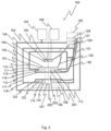
図1は、本発明の第1の実施形態によるテスト装置の断面図を示す。テスト装置100は、集積回路を含むウェハ102を保持するためのチャック101と、プローブカードホルダ104に取り付けられ、ウェハ102上の集積回路と電気的に接触するためのプローブカード103とを備える。プローブカード103は接触要素105を含み、接触要素105は、集積回路の接触パッドと電気的に接触状態になるよう構成することができる。集積回路の電気的テストは、プローブカード103に電気的に接続される電子テストユニット106で行われる。プローブカード103は、電子テストユニット106とウェハ102上の集積回路との間に電気経路を提供する。
Figure 1 shows a cross-sectional view of a test apparatus according to a first embodiment of the present invention. The
チャック101は、第1の端部および第2の端部を有する支柱107を含む移動手段を用いて、プローブカード103に対して移動されることができる。支柱107の第1の端部は、チャック101が支柱107の長手方向軸に対して垂直になるようにチャック101に取り付けられる。移動手段は、支柱107を3つの垂直方向に移動するための第1のアクチュエータ108、および支柱107をその長手方向軸の周りに回転させるための第2のアクチュエータ109も含む。第1のアクチュエータ108および第2のアクチュエータ109は、支柱107の第2の端部に取り付けられており、その運動は、支柱107を介してチャック101に伝達される。
The
チャック101およびプローブカード103は、第1の固定された部分111および第1の可動部分112を含む第1の放射シールド110の内部に配置される。第1の固定された部分111は、支柱107の第1の端部が第1の放射シールド110の内部へと延びるように支柱107が通過するよう構成される第1の開口部113を有する。第1の可動部分112は、支柱107が通過するように構成される第2の開口部114を有する。第1の可動部分112は、第1の固定された部分111の下端壁の下方に位置決めされ、第1の開口部113を覆うように支柱107に取り付けられている。第1の固定された部分111の下端壁には、第1の開口部113の周りにリップ115が設けられており、第1の可動部分112には、その外縁に配置され、リップ115に面するリップ116が設けられている。
The
第1の放射シールド110は、第2の固定された部分118および第2の可動部分119を含む第2の放射シールド117の内側に配置される。第1の放射シールド110の第1の固定された部分111は、第2の放射シールド117の第2の固定された部分118に機械的に取り付けられるが、それから断熱される。第2の固定された部分118は、支柱107が通過するように配置される第3の開口部120を有し、それにより、支柱107の第2の端部が第2の放射シールド117から延在する。第2の可動部分119は、支柱107が通過するように構成される第4の開口部121を有する。第2の可動部分119は、第2の固定された部分118の下端壁の上方に位置し、第3の開口部120を覆うように支柱107に取り付けられている。第2の固定された部分118の下端壁には、第3の開口部120の周りにリップ122が設けられ、第2の可動部分119には、その外縁に配置され、リップ122に面するリップ123が設けられている。
The
第2の放射シールド117は、真空チャンバ124の内側に配置される。第2の放射シールド117の第2の固定された部分118は、真空チャンバ124に取り付けられる。真空チャンバ124により、集積回路を制御された環境でテストすることができる。真空チャンバ124内の圧力は、真空ポンプ125で制御される。
The
テスト装置は、ウェハ102を所望のテスト温度に冷却し、集積回路のテスト中にテスト温度を維持するための冷却ユニット126を含む。冷却ユニット126は、3つの温度段127、128、および129を含み、その各々は、それが熱的に接続される部分に特定の温度を与えるように構成される。第1の温度段127は第1の放射シールド110に熱的に接続され、第2の温度段128は第2の放射シールド117に熱的に接続される。第1の温度段127で達成できる温度は、第2の温度段128で達成できる温度よりも低い。熱は、第1の放射シールド110から、第1の温度段127と第1の放射シールド110との間に接続される熱リンク130を介して伝達される。熱は、第2の放射シールド117から、第2の温度段128と第2の放射シールド117との間に接続される熱リンク131を介して伝達される。第3の温度段129は、チャック101およびプローブカード103に熱的に接続される。第3の温度段129で達成できる温度は、第1の温度段127で達成できる温度よりも低い。熱は、第3の温度段129とチャック101およびプローブカードホルダ104との間に接続される熱リンク132を介して、チャック101およびプローブカード103から離れるように伝達される。
The test apparatus includes a
図2は、本発明の第2の実施形態に係るテスト装置の断面図を示す。図2のテスト装置が図2のテスト装置と異なるのは、支柱107が3つの柱部分201、202、203を含む点、ならびに第1の可動部分112および第2の可動部分119が、開口部を有さない点である。柱部分201の第1の端部はチャック101に取り付けられ、柱部分201の第2の端部は第1の可動部分112に取り付けられている。柱部分202の第1の端部は第1の可動部分112に取り付けられており、柱部分202の第2の端部は第2の可動部分119に取り付けられている。柱部分203の第1の端部は第2の可動部分119に取り付けられており、柱部分203の第2の端部はアクチュエータ108および109に取り付けられている。
2 shows a cross-sectional view of a test apparatus according to a second embodiment of the present invention. The test apparatus of FIG. 2 differs from the test apparatus of FIG. 2 in that the
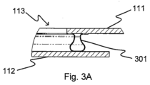
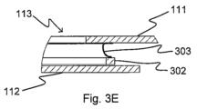
図3A~図3Eは、放射シールドの例示的な構造を示す。より具体的には、図3A~図3Eは、放射シールドの第1の固定された部分111と第1の可動部分112との間の閉じられた間隙の拡大図を示す。図3Aにおいて、第1の開口部113を取り囲むように第1の固定された部分111に取り付けられたシール301が示されている。シール301は、第1の可動部分112に対して押圧され、第1の固定された部分111と第1の可動部分112との間の間隙は閉じられる。図3Bの放射シールドが図3Aの放射シールドと異なる点は、第1の可動部分112が、間隙を介して漏洩する光子の数を低減するように、その外縁に配置されたリップ116を含むことである。図3Cの放射シールドが図3Aの放射シールドと異なる点は、第1の固定された部分111が、シール301が取り付けられるリップ115を含むことである。図3Dの放射シールドが図3Cの放射シールドと異なる点は、第1の可動部分112が、間隙を介して漏洩する光子の数を低減するように、その外縁に配置されたリップ116を含むことである。図3Eには、第1の固定された部分111と第1の可動部分112との間の間隙が、第1の固定された部分111に可撓性要素303を用いて取り付けられる中実リング302によって閉じられた構造が示されている。可撓性要素303は、第1の開口部113を取り囲む。
3A-3E show an exemplary structure of the radiation shield. More specifically, FIGS. 3A-3E show a close-up view of the closed gap between the first
本発明の有利な例示的実施形態のみが図に記載されている。本発明が上に提示された例のみに限定されず、本発明が以下に提示される特許請求の範囲内で変化し得ることは、当業者には明らかである。本発明のいくつかの可能な実施形態は、従属請求項に記載されており、それらは、本発明の保護の範囲をそのようなものとして制限するものと見なされるべきではない。 Only advantageous exemplary embodiments of the invention are depicted in the figures. It is clear to a person skilled in the art that the invention is not limited only to the examples presented above, but that the invention can vary within the scope of the claims presented below. Some possible embodiments of the invention are described in the dependent claims, which should not be considered as such limiting the scope of protection of the invention.
100 テスト装置、101 チャック、102 ウェハ、103 プローブカード、107 支柱、110 第1の放射シールド、111 第1の固定された部分、112 第1の可動部分、113 第1の開口部、124 真空チャンバ、126 冷却ユニット、201、202、203 支柱。 100 Test device, 101 Chuck, 102 Wafer, 103 Probe card, 107 Support, 110 First radiation shield, 111 First fixed part, 112 First movable part, 113 First opening, 124 Vacuum chamber, 126 Cooling unit, 201, 202, 203 Support.
Claims (16)
-真空チャンバと、
-集積回路を含むウェハを保持するためのチャックと、
-前記ウェハ上の前記集積回路に電気的に接触するためのプローブカードと、
-前記プローブカードに対して前記チャックを移動するための手段と、
-前記真空チャンバ内に配置され、前記チャックおよび前記プローブカードを囲む第1の放射シールドと、
-前記第1の放射シールドに熱的に接続される冷却ユニットとを備え、
-前記プローブカードに対して前記チャックを移動するための手段は、第1の端部および第2の端部を有する支柱を含み、前記支柱の前記第1の端部は前記チャックに取り付けられ、
-前記第1の放射シールドは、前記支柱が通過するように構成される第1の開口部を有する第1の固定された部分と、前記支柱に取り付けられ、前記第1の開口部を覆うように構成される第1の可動部分とを含む、テスト装置。 1. A test device comprising:
a vacuum chamber,
a chuck for holding a wafer containing integrated circuits;
- a probe card for electrically contacting the integrated circuits on the wafer;
- means for moving the chuck relative to the probe card;
a first radiation shield disposed within the vacuum chamber and surrounding the chuck and the probe card;
a cooling unit thermally connected to said first radiation shield,
- the means for moving the chuck relative to the probe card includes a post having a first end and a second end, the first end of the post being attached to the chuck;
a test apparatus, wherein the first radiation shield includes a first fixed part having a first opening configured for the pillar to pass through, and a first movable part attached to the pillar and configured to cover the first opening.
Applications Claiming Priority (2)
| Application Number | Priority Date | Filing Date | Title |
|---|---|---|---|
| EP19172489.7 | 2019-05-03 | ||
| EP19172489.7A EP3734301A1 (en) | 2019-05-03 | 2019-05-03 | Cryogenic wafer prober with movable thermal radiation shield |
Publications (2)
| Publication Number | Publication Date |
|---|---|
| JP2020184629A JP2020184629A (en) | 2020-11-12 |
| JP7561517B2 true JP7561517B2 (en) | 2024-10-04 |
Family
ID=66397100
Family Applications (1)
| Application Number | Title | Priority Date | Filing Date |
|---|---|---|---|
| JP2020080947A Active JP7561517B2 (en) | 2019-05-03 | 2020-05-01 | Test Equipment |
Country Status (6)
| Country | Link |
|---|---|
| US (1) | US11181574B2 (en) |
| EP (2) | EP3734301A1 (en) |
| JP (1) | JP7561517B2 (en) |
| KR (1) | KR102752734B1 (en) |
| CN (1) | CN111965516B (en) |
| CA (1) | CA3079000A1 (en) |
Families Citing this family (5)
| Publication number | Priority date | Publication date | Assignee | Title |
|---|---|---|---|---|
| CN113064046B (en) * | 2021-04-09 | 2021-11-26 | 深圳群芯微电子有限责任公司 | Photoelectric coupler radiation effect testing equipment and testing method |
| US11639957B2 (en) * | 2021-07-02 | 2023-05-02 | Northrop Grumman Systems Corporation | Planar ring radiation barrier for cryogenic wafer test system |
| US11480299B1 (en) | 2022-03-22 | 2022-10-25 | Anyon Systems Inc. | Cryostat and quantum computing system having same |
| TWI814491B (en) * | 2022-07-18 | 2023-09-01 | 財團法人國家實驗研究院 | Detachable protective structure of detection device |
| KR102824089B1 (en) * | 2023-08-09 | 2025-06-24 | 한국기초과학지원연구원 | Probestation apparatus |
Family Cites Families (24)
| Publication number | Priority date | Publication date | Assignee | Title |
|---|---|---|---|---|
| US5835997A (en) * | 1995-03-28 | 1998-11-10 | University Of South Florida | Wafer shielding chamber for probe station |
| DE19834854C2 (en) * | 1998-08-01 | 2000-06-29 | Karlsruhe Forschzent | Quasi-hemispherical Fabry-Perot resonator and method for operating the same |
| US6744268B2 (en) * | 1998-08-27 | 2004-06-01 | The Micromanipulator Company, Inc. | High resolution analytical probe station |
| US6580283B1 (en) * | 1999-07-14 | 2003-06-17 | Aehr Test Systems | Wafer level burn-in and test methods |
| US6700397B2 (en) * | 2000-07-13 | 2004-03-02 | The Micromanipulator Company, Inc. | Triaxial probe assembly |
| US6424141B1 (en) * | 2000-07-13 | 2002-07-23 | The Micromanipulator Company, Inc. | Wafer probe station |
| US7046025B2 (en) * | 2002-10-02 | 2006-05-16 | Suss Microtec Testsystems Gmbh | Test apparatus for testing substrates at low temperatures |
| DE10246282B4 (en) * | 2002-10-02 | 2005-12-29 | Suss Microtec Test Systems Gmbh | Prober for testing substrates at low temperatures |
| US20060266053A1 (en) * | 2005-05-25 | 2006-11-30 | General Electric Company | Apparatus for thermal shielding of a superconducting magnet |
| JP4319650B2 (en) * | 2005-07-29 | 2009-08-26 | 株式会社日立製作所 | Low temperature probe for NMR and NMR apparatus |
| US20090045829A1 (en) * | 2005-08-04 | 2009-02-19 | Sumitomo Electric Industries, Ltd. | Wafer holder for wafer prober and wafer prober equipped with same |
| US7652491B2 (en) * | 2006-11-17 | 2010-01-26 | Suss Microtec Test Systems Gmbh | Probe support with shield for the examination of test substrates under use of probe supports |
| KR100779029B1 (en) * | 2006-12-15 | 2007-11-23 | 세크론 주식회사 | Probe station and wafer inspection method using the same |
| TWI334486B (en) * | 2007-03-02 | 2010-12-11 | King Yuan Electronics Co Ltd | Test apparatus with heat-resistant lens kit |
| KR20090046086A (en) * | 2007-11-05 | 2009-05-11 | 지원호 | Automatic probe device |
| DE102008047337B4 (en) * | 2008-09-15 | 2010-11-25 | Suss Microtec Test Systems Gmbh | Method and device for testing a test substrate in a prober under defined thermal conditions |
| WO2010094719A1 (en) * | 2009-02-22 | 2010-08-26 | Mapper Lithography Ip B.V. | Charged particle lithography apparatus and method of generating vacuum in a vacuum chamber |
| JP5324339B2 (en) * | 2009-06-29 | 2013-10-23 | 泰弘 山田 | Semiconductor inspection and measurement equipment |
| WO2011159390A1 (en) * | 2010-06-07 | 2011-12-22 | Cascade Microtech, Inc. | High voltage chuck for a probe station |
| JP6076695B2 (en) * | 2012-10-30 | 2017-02-08 | 株式会社日本マイクロニクス | Inspection unit, probe card, inspection device, and control system for inspection device |
| CN106488792B (en) * | 2014-07-09 | 2020-11-27 | 布鲁弗斯低温学有限公司 | Regenerative capture stage, refrigerator including regenerative capture stage, and method of cleaning regenerative capture stage |
| KR102548778B1 (en) * | 2016-07-28 | 2023-06-27 | 세메스 주식회사 | Apparatus for inspecting semiconductor devices |
| DE102016214728B3 (en) * | 2016-08-09 | 2017-08-03 | Bruker Biospin Ag | NMR apparatus with cooled probe head components insertable through a vacuum lock in the cryostats of a superconducting magnet assembly, and methods of assembling and removing same |
| JP6827385B2 (en) * | 2017-08-03 | 2021-02-10 | 東京エレクトロン株式会社 | Inspection system |
-
2019
- 2019-05-03 EP EP19172489.7A patent/EP3734301A1/en not_active Withdrawn
-
2020
- 2020-04-15 CA CA3079000A patent/CA3079000A1/en active Pending
- 2020-04-23 EP EP20171032.4A patent/EP3734305B1/en active Active
- 2020-04-29 KR KR1020200052065A patent/KR102752734B1/en active Active
- 2020-04-29 US US16/861,257 patent/US11181574B2/en active Active
- 2020-04-30 CN CN202010368026.7A patent/CN111965516B/en active Active
- 2020-05-01 JP JP2020080947A patent/JP7561517B2/en active Active
Non-Patent Citations (5)
| Title |
|---|
| CHIAO MENG P ET AL,System design and implementation of the detector assembly of the Astro-H soft x-ray spectrometer,JOURNAL OF ASTRONOMICAL TELESCOPES, INSTRUMENTS,2018年03月19日,vol.4, no.2,pages 21404,DOI: 10.1117/1.JATIS.4.2.021404 |
| CPS-150-LN2/LHe-HV,2017年04月02日,pages 1-3,https://web.archive.org/web/20170402144621if_/http://microxact.com/wp-content/uploads/2016/05/CPS-150-LN2LHe-HV.pdf |
| FWP6 Probe Station Operating Guide,2005年06月01日,pages 1-70,https://www.equipx.net/uploads/Lakeshore%20Cryogenics/LakeshoreCryogenicsFWP6Manual.pdf |
| MICHAEL CYBEREY ET AL,Closeout report for Advanced Materials and On-wafer Chip Evaluation: 2nd Generation ALMA Superconducting Mixers,ALMA DEVELOPMENT STUDIES (CYCLE 3),2017年03月,pages 1- 44,https://science.nrao.edu/facilities/alma/alma-develop-old-022217/licht.pdf |
| RUSSELL DAMON ET AL,Cryogenic probe station for on-wafer characterization of electrical devices,REVIEW OF SCIENTIFIC INSTRUMENTS,AIP,2012年04月09日,vol. 83, no.4,pages 44703 - 44703,DOI: 10.1063/1.3700213 |
Also Published As
| Publication number | Publication date |
|---|---|
| EP3734305B1 (en) | 2024-08-07 |
| KR102752734B1 (en) | 2025-01-08 |
| US11181574B2 (en) | 2021-11-23 |
| CN111965516A (en) | 2020-11-20 |
| US20200348357A1 (en) | 2020-11-05 |
| EP3734305A1 (en) | 2020-11-04 |
| CN111965516B (en) | 2024-12-20 |
| EP3734301A1 (en) | 2020-11-04 |
| KR20200128358A (en) | 2020-11-12 |
| JP2020184629A (en) | 2020-11-12 |
| EP3734305C0 (en) | 2024-08-07 |
| CA3079000A1 (en) | 2020-11-03 |
Similar Documents
| Publication | Publication Date | Title |
|---|---|---|
| JP7561517B2 (en) | Test Equipment | |
| JP7557281B2 (en) | Test Equipment | |
| US5410162A (en) | Apparatus for and method of rapid testing of semiconductor components at elevated temperature | |
| JP5555633B2 (en) | Method for inspecting a test substrate under a predetermined temperature condition and an inspection apparatus capable of setting the temperature condition | |
| US11199575B2 (en) | Prober and probe card precooling method | |
| JPWO2021102181A5 (en) | ||
| EP3734304A1 (en) | Cryogenic probe station | |
| EP4187183A1 (en) | Refrigeration system | |
| EP3734302A1 (en) | Cryogenic wafer prober with camera, window and shutter | |
| US20120216559A1 (en) | Mounting device | |
| Andersson et al. | Lock-in thermography failure detection on multilayer ceramic capacitors after flex cracking and temperature–humidity–bias stress | |
| JP4045098B2 (en) | Process chamber assembly with reflective hot plate and pivot lid | |
| JP2000260839A (en) | Low temperature test equipment | |
| EP4506986A1 (en) | Wafer chuck, wafer prober and method for cooling a wafer | |
| JPH11145271A (en) | Wafer holder | |
| CN222914725U (en) | Sample cooling device and scanning electron microscope | |
| CN118231321B (en) | Semiconductor device with electrostatic chuck | |
| US20230420274A1 (en) | Radiatively-Cooled Substrate Holder | |
| JP2007101345A (en) | Card holder and prober | |
| JPH05343486A (en) | Inspection apparatus | |
| CN110823371A (en) | A fixing device for imaging element of hyperspectral detector | |
| JP2007171095A (en) | LCD substrate inspection equipment | |
| JP2007134403A (en) | Prober |
Legal Events
| Date | Code | Title | Description |
|---|---|---|---|
| A621 | Written request for application examination |
Free format text: JAPANESE INTERMEDIATE CODE: A621 Effective date: 20221216 |
|
| A131 | Notification of reasons for refusal |
Free format text: JAPANESE INTERMEDIATE CODE: A131 Effective date: 20240305 |
|
| TRDD | Decision of grant or rejection written | ||
| A01 | Written decision to grant a patent or to grant a registration (utility model) |
Free format text: JAPANESE INTERMEDIATE CODE: A01 Effective date: 20240827 |
|
| A61 | First payment of annual fees (during grant procedure) |
Free format text: JAPANESE INTERMEDIATE CODE: A61 Effective date: 20240924 |
|
| R150 | Certificate of patent or registration of utility model |
Ref document number: 7561517 Country of ref document: JP Free format text: JAPANESE INTERMEDIATE CODE: R150 |