JP7554075B2 - Operational Amplifier - Google Patents
Operational Amplifier Download PDFInfo
- Publication number
- JP7554075B2 JP7554075B2 JP2020142809A JP2020142809A JP7554075B2 JP 7554075 B2 JP7554075 B2 JP 7554075B2 JP 2020142809 A JP2020142809 A JP 2020142809A JP 2020142809 A JP2020142809 A JP 2020142809A JP 7554075 B2 JP7554075 B2 JP 7554075B2
- Authority
- JP
- Japan
- Prior art keywords
- transistor
- noise
- circuit
- resistor
- operational amplifier
- Prior art date
- Legal status (The legal status is an assumption and is not a legal conclusion. Google has not performed a legal analysis and makes no representation as to the accuracy of the status listed.)
- Active
Links
- 239000003990 capacitor Substances 0.000 claims description 62
- 230000001629 suppression Effects 0.000 claims description 48
- 238000001514 detection method Methods 0.000 claims description 45
- 230000003071 parasitic effect Effects 0.000 claims description 12
- 230000035945 sensitivity Effects 0.000 claims description 8
- 230000009471 action Effects 0.000 claims description 5
- 230000008859 change Effects 0.000 description 47
- 238000010586 diagram Methods 0.000 description 27
- 238000012795 verification Methods 0.000 description 18
- 230000000694 effects Effects 0.000 description 10
- 239000007787 solid Substances 0.000 description 9
- 230000007423 decrease Effects 0.000 description 5
- 230000009467 reduction Effects 0.000 description 4
- 230000004044 response Effects 0.000 description 4
- 101150016367 RIN1 gene Proteins 0.000 description 3
- 230000000903 blocking effect Effects 0.000 description 3
- 239000002131 composite material Substances 0.000 description 3
- 238000011160 research Methods 0.000 description 3
- 101150033693 Pdlim1 gene Proteins 0.000 description 2
- 230000007257 malfunction Effects 0.000 description 2
- 238000005259 measurement Methods 0.000 description 2
- 101100420776 Arabidopsis thaliana SYN1 gene Proteins 0.000 description 1
- VUDQSRFCCHQIIU-UHFFFAOYSA-N DIF1 Natural products CCCCCC(=O)C1=C(O)C(Cl)=C(OC)C(Cl)=C1O VUDQSRFCCHQIIU-UHFFFAOYSA-N 0.000 description 1
- 101150001108 DIF1 gene Proteins 0.000 description 1
- 102100034583 Dolichyl-diphosphooligosaccharide-protein glycosyltransferase subunit 1 Human genes 0.000 description 1
- 101000848781 Homo sapiens Dolichyl-diphosphooligosaccharide-protein glycosyltransferase subunit 1 Proteins 0.000 description 1
- 230000003321 amplification Effects 0.000 description 1
- 230000005540 biological transmission Effects 0.000 description 1
- 230000015556 catabolic process Effects 0.000 description 1
- 238000006731 degradation reaction Methods 0.000 description 1
- 238000013461 design Methods 0.000 description 1
- 230000006866 deterioration Effects 0.000 description 1
- 238000002474 experimental method Methods 0.000 description 1
- PCHJSUWPFVWCPO-UHFFFAOYSA-N gold Chemical compound [Au] PCHJSUWPFVWCPO-UHFFFAOYSA-N 0.000 description 1
- 239000010931 gold Substances 0.000 description 1
- 229910052737 gold Inorganic materials 0.000 description 1
- 230000036039 immunity Effects 0.000 description 1
- 238000002347 injection Methods 0.000 description 1
- 239000007924 injection Substances 0.000 description 1
- 238000000034 method Methods 0.000 description 1
- 238000012986 modification Methods 0.000 description 1
- 230000004048 modification Effects 0.000 description 1
- 238000003199 nucleic acid amplification method Methods 0.000 description 1
- 239000004065 semiconductor Substances 0.000 description 1
- 239000000243 solution Substances 0.000 description 1
- 238000012360 testing method Methods 0.000 description 1
Images


Landscapes
- Amplifiers (AREA)
Description
本発明は、演算増幅器に係り、特に、高周波外来ノイズに起因する出力特性の劣化防止、動作の安定性確保等を図ったものに関する。 The present invention relates to an operational amplifier, and in particular to one that aims to prevent degradation of output characteristics caused by high-frequency external noise and ensure operational stability.
従来、演算増幅器における高周波外来ノイズに対する方策としては、ノイズが入力端子に混入することに着目して対策を施したものが多い。例えば、特許文献1等には、入力に混入する高周波外来ノイズをコンデンサと抵抗器で構成されるローパスフィルタ(LPF)で軽減するものが提案されている。
Conventionally, many of the measures taken to deal with high-frequency external noise in operational amplifiers focus on the fact that noise gets mixed in with the input terminal. For example,
特許文献1においては、同文献で開示されたローパスフィルタによる高周波外来ノイズ対策は、図10に示された回路を用いて高周波外来ノイズの混入について検証した結果を反映したものである旨が述べられている。
図10に示された検証回路は、演算増幅器OP1の非反転入力端子に、DCカット用コンデンサCA1を介してAC電圧源RFが接続されているところに特徴を有するものである。
The verification circuit shown in FIG. 10 is characterized in that an AC voltage source RF is connected to the non-inverting input terminal of an operational amplifier OP1 via a DC blocking capacitor CA1.
また、図11には、演算増幅器OP1の具体的な回路構成例が示されている。
この図11に示された回路は、特許文献1において演算増幅器OP1の従来回路として開示されているものと基本的に同一構成のものであるが、図11においては、電流分配用のカレントミラー回路の具体回路構成も示されたものとなっている。
この電流分配用のカレントミラー回路は、カレントミラー元であるトランジスタQ109と電流源CS1とを用いて構成されており、トランジスタQ109に電流源CS1が接続されて、この電流源CS1の電流がトランジスタQ110~Q117にミラーされている。
FIG. 11 shows a specific example of the circuit configuration of the operational amplifier OP1.
The circuit shown in FIG. 11 has basically the same configuration as that disclosed in
This current mirror circuit for current distribution is configured using a transistor Q109, which is the source of the current mirror, and a current source CS1. The current source CS1 is connected to the transistor Q109, and the current of this current source CS1 is mirrored to the transistors Q110 to Q117.
図12には、図10に示された検証回路において、AC電圧源RFによりAC電圧を演算増幅器OP1に印加した場合の出力電圧Voutの変化の測定結果が示されている。なお、AC電圧源RFの電圧振幅は0.2Vppである。
同図によれば、出力電圧Voutは、周波数が低い領域では0V付近で安定しているが、周波数が高くなるにつれて変動することが確認できる。この出力電圧Voutの変動は、演算増幅器の後段の集積回路において誤動作を招く原因となる。
Fig. 12 shows the measurement results of the change in the output voltage Vout when an AC voltage is applied to the operational amplifier OP1 by the AC voltage source RF in the verification circuit shown in Fig. 10. The voltage amplitude of the AC voltage source RF is 0.2 Vpp.
According to the figure, it can be seen that the output voltage Vout is stable near 0 V in the low frequency region, but fluctuates as the frequency increases. This fluctuation in the output voltage Vout can cause malfunctions in integrated circuits downstream of the operational amplifier.
かかる出力電圧Voutの変動対策として、特許文献1においては、図13に示されたように、反転入力端子INMとトランジスタQ1のベースとの間に抵抗器Rin1を、非反転入力端子INPとトランジスタQ2のベースとの間に抵抗器Rin2を、それぞれ挿入した構成が開示されている。
上述の構成において、トランジスタQ1、Q2のベースと負電源端子VEEとの間には、寄生容量Cin1、Cin2が存在する。
その結果、抵抗器Rin1、Rin2と寄生容量Cin1、Cin2とでローパスフィルタ(LPF)が構成され、それによる高周波外来ノイズの低減によって出力電圧Voutの変動抑制が可能となっている。
As a countermeasure against such fluctuations in the output voltage Vout,
In the above-mentioned configuration, parasitic capacitances Cin1 and Cin2 exist between the bases of the transistors Q1 and Q2 and the negative power supply terminal VEE.
As a result, a low pass filter (LPF) is formed by the resistors Rin1 and Rin2 and the parasitic capacitances Cin1 and Cin2, which reduces high frequency external noise and makes it possible to suppress fluctuations in the output voltage Vout.
本願発明者は、実際に図13の構成における高周波外来ノイズの低減効果の検証を行った。図14には、その検証結果である入力周波数変化に対する出力電圧Voutの変化特性が示されている。すなわち、同図において、実線の特性線は、図13に示された回路構成における入力周波数変化に対する出力電圧Voutの変化特性であり、対策がない場合(点線の特性線)に比して、高周波外来ノイズに対する一定の低減効果が確認できる。 The inventors of the present application actually verified the effect of reducing high-frequency external noise in the configuration of FIG. 13. FIG. 14 shows the result of the verification, ie, the change characteristic of the output voltage Vout with respect to the change in input frequency. That is, in the figure, the solid characteristic line is the change characteristic of the output voltage Vout with respect to the change in input frequency in the circuit configuration shown in FIG. 13, and a certain reduction effect on high-frequency external noise can be confirmed compared to the case where no countermeasure is taken (dotted characteristic line).
ところが、高周波外来ノイズが混入するのは入力端子だけとは限らず、例えば、電源ラインに混入する可能性を否定できない。特に、近年の車載半導体においては、電源ラインにおける高周波外来ノイズに対する高い耐性が求められる場合が増加している。
本願発明者は、かかる観点から、先の図13に示された演算増幅器における電源ラインへの高周波外来ノイズ混入の際の出力電圧Voutの挙動を検証した。
However, high-frequency external noise can enter not only input terminals, but also the power supply line. In particular, there is an increasing demand for high resistance to high-frequency external noise in the power supply line for in-vehicle semiconductors in recent years.
From this perspective, the inventors of the present application have examined the behavior of the output voltage Vout when high-frequency external noise is mixed into the power supply line in the operational amplifier shown in FIG.
図15には、検証に用いた回路例が示されており、同図を参照しつつ検証内容について説明する。
まず、図15に示された回路例において、演算増幅器OP1は、先の図13の回路構成のものである。演算増幅器OP1の端子にはインダクタンスL1~L5が付加されているが、これらは、パッケージングされた演算増幅器OP1に用いられている金線のインダクタンスを等価的に表したものである。
FIG. 15 shows an example of a circuit used in the verification, and the verification content will be described with reference to this figure.
First, in the circuit example shown in Fig. 15, the operational amplifier OP1 has the circuit configuration shown in Fig. 13. Inductances L1 to L5 are added to the terminals of the operational amplifier OP1, which are equivalent to the inductances of the gold wires used in the packaged operational amplifier OP1.
図15に示された回路例は、演算増幅器OP1によりボルテージフォロア回路が構成されており、反転入力端子INMは寄生インダクタンスL2、L5を介して出力端子OUTに接続されている。
一方、非反転入力端子INPは、寄生インダクタンスL3を介してDC電圧源V2=6Vに接続されている。
In the circuit example shown in FIG. 15, a voltage follower circuit is configured by an operational amplifier OP1, and an inverting input terminal INM is connected to an output terminal OUT via parasitic inductances L2 and L5.
On the other hand, the non-inverting input terminal INP is connected to a DC voltage source V2=6 V via a parasitic inductance L3.
また、負電源端子VEEは、寄生インダクタンスL4を介してグランドに接続されている。
正電源端子VCCは、寄生インダクタンスL1及びインダクタLA1を介してDC電圧源V1=12Vに接続されると共に、DCカット用コンデンサCA1を介してAC電圧源RFに接続されている。インダクタLA1は、DC電圧源への高周波信号を遮断する。
AC電圧源RFは、高周波外来ノイズを模しており、出力はPin(dBm)である。
Moreover, the negative power supply terminal VEE is connected to ground via a parasitic inductance L4.
The positive power supply terminal VCC is connected to a DC voltage source V1=12V via a parasitic inductance L1 and an inductor LA1, and is also connected to an AC voltage source RF via a DC blocking capacitor CA1. The inductor LA1 blocks high frequency signals to the DC voltage source.
The AC voltage source RF mimics high frequency external noise and has an output of Pin (dBm).
ここで、DC電圧源V1=12Vと、DCカットコンデンサCA1と、寄生インダクタンスL1とが電気的に導通状態とされるノードを、以下、説明の便宜上”電源ライン”と称する。
以下、この電源ラインにおける高周波外来ノイズの混入に対する演算増幅器OP1への影響に関する検証について説明する。
Here, for convenience of explanation, a node where the DC voltage source V1=12V, the DC blocking capacitor CA1, and the parasitic inductance L1 are electrically connected is referred to as a "power supply line" hereinafter.
The following describes verification of the effect of high-frequency external noise on the power supply line on the operational amplifier OP1.
かかる検証は、AC電圧源RFからの入力電力を増加した場合の出力電圧VoutのDCレベルを計測することで行う。
例えば、図15の回路において、AC電圧源RFからの入力電圧が無い場合、出力電圧Voutが6Vとなることは自明である。しかし、AC電圧源RFからの入力電力Pinが増加すると、演算増幅器OP1は何等かの影響を受け、出力電圧Voutは変動を来す。
This verification is performed by measuring the DC level of the output voltage Vout when the input power from the AC voltage source RF is increased.
15, when there is no input voltage from the AC voltage source RF, it is obvious that the output voltage Vout is 6 V. However, when the input power Pin from the AC voltage source RF increases, the operational amplifier OP1 is somehow affected, and the output voltage Vout fluctuates.
図16には、図15の回路における検証結果として、電源ラインへのAC入力電力Pinの変化に対する出力電圧Voutの変化特性が点線の特性線により示されている。
この検証結果は、入力電力Pinを変化させた際の、出力電圧Voutの変化を計測した結果である。
なお、AC電圧源RFの周波数は0.5GHzである。
FIG. 16 shows, as a verification result for the circuit of FIG. 15, the change characteristic of the output voltage Vout relative to the change in the AC input power Pin to the power supply line, as indicated by a dotted characteristic line.
This verification result was obtained by measuring the change in the output voltage Vout when the input power Pin was changed.
The frequency of the AC voltage source RF is 0.5 GHz.
演算増幅器OP1は、先に図13に示されたように入力端子に対する高周波外来ノイズに対する対策が施されたものであるが、図16に示された検証結果においては、AC電圧源RFの入力電力Pinが28dBm付近になると、出力電圧Voutは大きく変動し始めていることが確認できる。
これは、高周波外来ノイズが電源ラインに混入すると、出力電圧Voutが変動することを意味するものである。
As shown in FIG. 13, the operational amplifier OP1 has been provided with measures against high frequency external noise at its input terminal. However, in the verification results shown in FIG. 16, it can be seen that when the input power Pin of the AC voltage source RF reaches approximately 28 dBm, the output voltage Vout begins to fluctuate significantly.
This means that when high-frequency external noise is introduced into the power supply line, the output voltage Vout fluctuates.
このような出力電圧Voutの変動は、実使用において誤動作を招く原因となる。なお、このようにAC電源などを用いて、特定の端子に高周波外来ノイズを印加する実験は、Direct Power Injectionと称され、DPIと略称されることもある。
本願発明者は、多くの試験を積み重ね、鋭意研究の結果、図17に示された回路構成を用いることで、正電源端子への高周波外来ノイズ耐性の高い演算増幅器を得ることができる結論を導くに至った。
Such fluctuations in the output voltage Vout can cause malfunctions in actual use. Note that an experiment in which high-frequency external noise is applied to a specific terminal using an AC power supply or the like is called Direct Power Injection, sometimes abbreviated as DPI.
As a result of extensive testing and intensive research, the inventors of the present application have come to the conclusion that by using the circuit configuration shown in FIG. 17, it is possible to obtain an operational amplifier that has high resistance to high frequency external noise at the positive power supply terminal.
この図17に示された回路構成は、コンデンサCX1と抵抗器RX1、RX11及びダイオードDX1を設けると共に、それぞれ、所定の条件を満たす回路定数を選定することで、次述するように高い高周波外来ノイズ耐性を得ることができるものとなっている。 The circuit configuration shown in Figure 17 includes a capacitor CX1, resistors RX1 and RX11, and a diode DX1, and by selecting circuit constants that satisfy specific conditions, it is possible to obtain high resistance to high-frequency external noise, as described below.
以下、図18に示された特性線図を参照しつつ、図17に示された回路構成の演算増幅器の高周波外来ノイズ耐性について説明する。
図18は、演算増幅器における高周波外来ノイズの入力電力変化に対する出力電圧の変化特性例を示す特性線図であり、横軸は電源ラインへの高周波外来ノイズのAC入力電力を、縦軸は出力電圧を、それぞれ示している。
Hereinafter, the resistance to high-frequency external noise of the operational amplifier having the circuit configuration shown in FIG. 17 will be described with reference to the characteristic diagram shown in FIG.
FIG. 18 is a characteristic diagram showing an example of the change in output voltage versus change in input power of high-frequency external noise in an operational amplifier, where the horizontal axis represents the AC input power of high-frequency external noise to the power supply line, and the vertical axis represents the output voltage.
同図には、先に図13に示された回路構成の演算増幅器(従来回路)における高周波外来ノイズのAC入力電力変化に対する出力電圧Voutの変化例が点線の特性線により、また、図17の回路構成の演算増幅器(提案回路)における高周波外来ノイズのAC入力電力変化に対する出力電圧Voutの変化例が実線の特性線により、それぞれ示されている。なお、いずれの特性線も高周波外来ノイズの周波数が0.5GHzとした場合のものである。 In the figure, the dotted characteristic line shows an example of the change in the output voltage Vout in response to changes in the AC input power of high-frequency external noise in an operational amplifier (conventional circuit) having the circuit configuration shown in Figure 13, while the solid characteristic line shows an example of the change in the output voltage Vout in response to changes in the AC input power of high-frequency external noise in an operational amplifier (proposed circuit) having the circuit configuration shown in Figure 17. Note that both characteristic lines are for the case where the frequency of the high-frequency external noise is 0.5 GHz.
まず、図13に示された回路構成の演算増幅器の場合、AC入力電力が28dBm付近からAC入力電力の増加に伴い出力電力Voutが低下する傾向を示している。
これに対して、図17に示された回路構成の演算増幅器の場合、AC入力電力が33dBmとなるまでは出力電力Voutをほぼ一定に維持できていることが確認できるものとなっている。
First, in the case of the operational amplifier having the circuit configuration shown in FIG. 13, the output power Vout shows a tendency to decrease as the AC input power increases from about 28 dBm.
In contrast to this, in the case of the operational amplifier having the circuit configuration shown in FIG. 17, it can be confirmed that the output power Vout can be maintained almost constant until the AC input power reaches 33 dBm.
しかしながら、本願発明者のさらなる研究の結果、特定の高周波0.61GHzにおいて正電源端子にAC電力を入射すると、出力電圧Voutが著しく悪化することを見出すに至った。
図19には、この事を説明する特性線図が示されており、以下、同図を参照しつつ、上述の現象について説明する。
まず、図19は、電源ラインへのAC入力電力Pinの変化に対する出力電圧Voutの変化特性を示した特性線図である。
同図において、横軸は電源ラインへの高周波外来ノイズのAC入力電力を、縦軸は出力電圧を、それぞれ示している。
However, as a result of further research by the present inventors, it has been discovered that when AC power is applied to the positive power supply terminal at a specific high frequency of 0.61 GHz, the output voltage Vout is significantly degraded.
FIG. 19 shows a characteristic diagram for explaining this, and the above-mentioned phenomenon will be explained below with reference to this figure.
First, FIG. 19 is a characteristic diagram showing the change characteristic of the output voltage Vout with respect to the change in the AC input power Pin to the power supply line.
In the figure, the horizontal axis represents the AC input power of high frequency external noise to the power supply line, and the vertical axis represents the output voltage.
図19において、点線の特性線は、図17に示された回路において、AC入力電力の周波数を0.61GHzとした場合の電源ラインへのAC入力電力Pinの変化に対する出力電圧Voutの変化特性を示している。
また、二点鎖線の特性線は、同回路において、AC入力電力の周波数を0.5GHzとした場合の電源ラインへのAC入力電力Pinの変化に対する出力電圧Voutの変化特性を、実線の特性線は、AC入力電力の周波数を0.7GHzとした場合の電源ラインへのAC入力電力Pinの変化に対する出力電圧Voutの変化特性を、それぞれ示している。
19, the dotted characteristic line indicates the change characteristic of the output voltage Vout with respect to the change in the AC input power Pin to the power supply line in the circuit shown in FIG. 17 when the frequency of the AC input power is 0.61 GHz.
In addition, the dashed double-dashed characteristic line indicates the change characteristic of the output voltage Vout in response to a change in the AC input power Pin to the power supply line when the frequency of the AC input power is 0.5 GHz, and the solid characteristic line indicates the change characteristic of the output voltage Vout in response to a change in the AC input power Pin to the power supply line when the frequency of the AC input power is 0.7 GHz.
図19によれば、AC入力電力の周波数が0.5GHz、0.7GHzの場合、入力電力が33dBm付近までは出力電圧Voutが一定値を維持できるのに対して、周波数0.61GHzでは入力電力29dBm付近までしか出力電圧Voutを一定値に維持することができず、入力電力29dBm以降は急激な電圧低下が生じていることが確認できる。
すなわち、図17に示された回路の演算増幅器は、周波数0.61GHzの高周波外来ノイズが正電源端子に混入した際、出力電圧Voutの大きな変動が生ずることとなる。
According to FIG. 19 , when the frequency of the AC input power is 0.5 GHz and 0.7 GHz, the output voltage Vout can be maintained at a constant value up to an input power of approximately 33 dBm, whereas at a frequency of 0.61 GHz, the output voltage Vout can only be maintained at a constant value up to an input power of approximately 29 dBm, and it can be confirmed that a rapid voltage drop occurs after the input power reaches 29 dBm.
That is, in the operational amplifier of the circuit shown in FIG. 17, when high-frequency external noise with a frequency of 0.61 GHz is mixed into the positive power supply terminal, a large fluctuation occurs in the output voltage Vout.
本願発明者は、このような特定の周波数0.61GHzにおいてのみノイズ耐性が大幅に劣化する原因について、鋭意研究の結果、演算増幅器の終段部分に設けられている過電流保護回路に原因があることを導くに至った。
図20には、過電流保護回路CLim1に該当する部分を点線で囲んだ図17と同一の回路構成が示されている。
同回路において、トランジスタQ14~Q16、及び、抵抗器R1,R2から構成される部分が過電流保護回路CLim1であり、本願発明者は、特定の周波数0.61GHzにおいてのみ、過電流保護回路CLim1が極端にONし易い状態に陥ることを突き止めるに至った。
As a result of extensive research, the inventors of the present application have concluded that the cause of the significant deterioration in noise resistance only at this specific frequency of 0.61 GHz lies in the overcurrent protection circuit provided at the final stage of the operational amplifier.
FIG. 20 shows the same circuit configuration as FIG. 17, with the portion corresponding to the overcurrent protection circuit CLim1 surrounded by a dotted line.
In this circuit, the portion consisting of transistors Q14 to Q16 and resistors R1 and R2 constitutes the overcurrent protection circuit CLim1, and the inventors of the present application have discovered that only at a specific frequency of 0.61 GHz does the overcurrent protection circuit CLim1 fall into a state in which it is extremely likely to turn ON.
換言すれば、図20に示された回路構成の演算増幅器の正電源端子に高周波外来ノイズが混入すると、例えノイズ振幅が小さくとも、そのノイズ周波数が0.61GHzである場合には、過電流保護回路CLim1はON状態となり、出力電圧Voutが悪化するという現象が生ずる。 In other words, when high-frequency external noise is introduced into the positive power supply terminal of the operational amplifier in the circuit configuration shown in FIG. 20, even if the noise amplitude is small, if the noise frequency is 0.61 GHz, the overcurrent protection circuit CLim1 will be turned on, causing the output voltage Vout to deteriorate.
トランジスタQ14~Q16、抵抗器R1,R2から構成される過電流保護回路CLim1の動作は、従来から良く知られている回路(例えば、非特許文献1等参照)であるので、以下、概括的に説明する。
この過電流保護回路CLim1は、抵抗器R2に流れる電流Ioutが下記する式1の条件を満たすまで増加した際にON状態となる。
The operation of the overcurrent protection circuit CLim1, which is composed of the transistors Q14 to Q16 and the resistors R1 and R2, is a well-known circuit (see, for example, Non-Patent Document 1), and therefore will be briefly described below.
The overcurrent protection circuit CLim1 is turned on when the current Iout flowing through the resistor R2 increases to a value satisfying the condition of the following
Vbe(Q14)=R2×Iout・・・式1
Vbe(Q14)=R2×Iout...
ここで、Vbe(Q14)は、トランジスタQ14のベース・エミッタ間電圧であって、具体的には、約0.6Vである。
また、R2は、抵抗器R2の抵抗値、Ioutは、抵抗器R2を介して流れる出力電流の電流値である。
出力電流Ioutが増加し、式1の条件を満たす状態となった際に、トランジスタQ14のコレクタ電流IcQ14が流れ、トランジスタQ15のベース電流IbQ15が制限されることとなる(図20参照)。
Here, Vbe(Q14) is the base-emitter voltage of the transistor Q14, and is specifically about 0.6V.
Furthermore, R2 is the resistance value of the resistor R2, and Iout is the current value of the output current flowing through the resistor R2.
When the output current Iout increases and satisfies the condition of
その結果、トランジスタQ15とダーリントン接続されたトラジスタQ16のエミッタ電流は、式1を満たす出力電流Ioutを越える大きな電流を流さなくなる。
かかる動作を有する過電流保護回路CLim1の回路構成は、フィードバック回路が構成されたものとなっている。
このような回路構成であることを考慮しつつ、周波数0.61GHzのノイズが混入した際に、この演算増幅器の出力電圧Voutが低下する理由を、図21を参照しつつ説明する。
As a result, the emitter current of the transistor Q16 connected in a Darlington configuration with the transistor Q15 does not flow a current larger than the output current Iout that satisfies the formula (1).
The circuit configuration of the overcurrent protection circuit CLim1 having such an operation is configured as a feedback circuit.
Taking into consideration such a circuit configuration, the reason why the output voltage Vout of this operational amplifier drops when noise with a frequency of 0.61 GHz is mixed in will be described with reference to FIG.
まず、過電流保護回路CLim1に周波数0.61GHzの僅かな電圧振幅の信号が正電源端子に混入すると、過電流保護回路CLim1がON状態になる。
過電流保護回路CLim1がONしていない通常の状態であれば、トランジスタQ10のコレクタ電位は、トランジスタQ15,Q16及び抵抗器R2を介して出力端子OUTに伝達される。
しかし、過電流保護回路CLim1がONした状態であると、トランジスタQ15のベース電流IbQ15が制限されるため、トランジスタQ15のベースからエミッタへ、トランジスタQ10の電圧信号を伝達することができなくなる。
First, when a signal with a small voltage amplitude and a frequency of 0.61 GHz is input to the positive power supply terminal of the overcurrent protection circuit CLim1, the overcurrent protection circuit CLim1 is turned on.
In a normal state where the overcurrent protection circuit CLim1 is not turned on, the collector potential of the transistor Q10 is transmitted to the output terminal OUT via the transistors Q15 and Q16 and the resistor R2.
However, when the overcurrent protection circuit CLim1 is in the ON state, the base current IbQ15 of the transistor Q15 is limited, so that the voltage signal of the transistor Q10 cannot be transmitted from the base to the emitter of the transistor Q15.
そのため、トランジスタQ10のコレクタ電位の信号は、別の伝達ルートとして、トランジスタQ17を介して出力端子OUTに伝達されることとなる。
また、過電流保護回路CLim1がONしてない通常の状態であれば、トランジスタQ117コレクタ電流IcQ117は、一定程度、トランジスタQ10のコレクタに流れる。しかし、過電流保護回路CLim1がONすると、トランジスタQ14のコレクタ電流IcQ14にトラジスタQ117のコレクタ電流IcQ117の大部分が費やされる。その結果、トランジスタQ10のコレクタ電流IcQ10は、トランジスタQ17のベース電流IbQ17でのみ補われることとなる。
Therefore, the signal of the collector potential of the transistor Q10 is transmitted to the output terminal OUT via the transistor Q17 as another transmission route.
In addition, in a normal state where the overcurrent protection circuit Clim1 is not ON, a certain amount of the collector current IcQ117 of the transistor Q117 flows to the collector of the transistor Q10. However, when the overcurrent protection circuit Clim1 is ON, most of the collector current IcQ117 of the transistor Q117 is consumed by the collector current IcQ14 of the transistor Q14. As a result, the collector current IcQ10 of the transistor Q10 is supplemented only by the base current IbQ17 of the transistor Q17.
しかし、トランジスタQ17のベース電流IbQ17の大きさは限られており、トラジスタQ10のコレクタ電流IcQ10は、過電流保護回路CLim1がONする前に比較して減少せざる得なくなる。
一方、トランジスタQ10のベース電流IbQ10は、過電流保護回路CLim1のON、OFFに拘わらず一定の大きさである。
したがって、トランジスタQ10のベース電流IbQ10が一定である一方、コレクタ電流IcQ10が減少するという状態に陥る。
However, the magnitude of the base current IbQ17 of the transistor Q17 is limited, and the collector current IcQ10 of the transistor Q10 is inevitably reduced compared to before the overcurrent protection circuit CLim1 was turned ON.
On the other hand, the base current IbQ10 of the transistor Q10 has a constant magnitude regardless of whether the overcurrent protection circuit CLim1 is ON or OFF.
Therefore, the base current IbQ10 of the transistor Q10 remains constant while the collector current IcQ10 decreases.
そして、トランジスタQ10のコレクタ電位は、コレクタ電流IcQ10を減少させるために低下する。このトランジスタQ10のコレクタ電位の低下は、トランジスタ17を介して出力端子OUTに伝達され、結果として、出力電圧Voutが低下する現象が表れる。以上が周波数0.61GHzのノイズが正電源端子に混入した際に出力電圧Voutが低下する理由である。
The collector potential of transistor Q10 then drops to reduce collector current IcQ10. This drop in the collector potential of transistor Q10 is transmitted to output terminal OUT via
上述の問題を解決する方策としては、過電流保護回路CLim1が簡単にONしないように、電流検出抵抗器R2の抵抗値を小さくする方法が考えられる。しかし、抵抗器R2の抵抗値を小さくすることは、先の式1を参照すると、出力電流Ioutの増大を意味する。
演算増幅器の出力電流Ioutの増大は、出力電流Ioutを所望の値以下に抑えて演算増幅器や周囲の回路を保護するという過電流保護回路の機能が果たせなくなるという問題を招くこととなる。
One possible solution to the above problem is to reduce the resistance of the current detection resistor R2 so that the overcurrent protection circuit CLim1 does not easily turn on. However, referring to the
An increase in the output current Iout of the operational amplifier causes a problem in that the overcurrent protection circuit cannot perform its function of protecting the operational amplifier and surrounding circuits by suppressing the output current Iout to a desired value or less.
本発明は、上記実状に鑑みてなされたもので、過電流保護回路の出力電流値の不要な増加を招くことなく、電源ラインに高周波外来ノイズが混入しても安定した出力特性を得ることのできる演算増幅器を提供するものである。 The present invention has been made in consideration of the above situation, and provides an operational amplifier that can obtain stable output characteristics even when high-frequency external noise is mixed into the power supply line, without causing an unnecessary increase in the output current value of the overcurrent protection circuit.
上記本発明の目的を達成するため、本発明に係る演算増幅器は、
非反転入力端子と反転入力端子間に印加された入力信号の差動増幅可能に構成されてなる演算増幅器であって、
前記演算増幅器は、出力段における過電流を検出すると共に、前記過電流が検出された場合に前記出力段の電流抑圧を可能としてなる過電流保護回路を有し、前記過電流保護回路は、所望の高周波領域における過電流検出の感度を抑制する高周波ノイズ対策回路が設けられてなり、
前記過電流保護回路は、過電流検出用トランジスタと、前記出力段に流れる電流検出のために前記出力段に設けられた検出用抵抗器とを有し、前記過電流検出用トランジスタのベースとエミッタ間に前記検出用抵抗器が接続されて、前記検出用抵抗器における過電流が検出された場合に前記過電流検出用トランジスタにより前記出力段の電流を低減するよう構成されてなり、
前記高周波ノイズ対策回路は、前記検出用抵抗器と並列接続された第1のノイズ対策コンデンサを有してなり、
前記第1のノイズ対策コンデンサの容量値CX2は、
不等式CX2>1/(2π×2
1/2
×fc×R2)を満たす値に設定され、
前記不等式におけるfcは、除去する高周波ノイズの周波数、前記不等式におけるR2は、前記検出用抵抗器の抵抗値であり、
前記検出用抵抗器と前記第1のノイズ対策コンデンサとの並列接続部分におけるインピーダンスの低下により前記過電流保護回路における前記高周波領域での過電流検出感度を低下せしめることで前記高周波ノイズに起因する出力電圧の変動抑圧を図ったものである。
In order to achieve the above object of the present invention, an operational amplifier according to the present invention comprises:
An operational amplifier configured to be capable of differentially amplifying an input signal applied between a non-inverting input terminal and an inverting input terminal,
the operational amplifier has an overcurrent protection circuit that detects an overcurrent in an output stage and enables current suppression in the output stage when the overcurrent is detected, the overcurrent protection circuit being provided with a high-frequency noise suppression circuit that suppresses sensitivity of overcurrent detection in a desired high-frequency region;
the overcurrent protection circuit includes an overcurrent detection transistor and a detection resistor provided in the output stage for detecting a current flowing through the output stage, the detection resistor is connected between a base and an emitter of the overcurrent detection transistor, and when an overcurrent is detected in the detection resistor, the overcurrent detection transistor reduces a current in the output stage;
the high frequency noise countermeasure circuit includes a first noise countermeasure capacitor connected in parallel with the detection resistor,
The capacitance value CX2 of the first noise suppression capacitor is
It is set to a value that satisfies the inequality CX2>1/(2π×2 1/2 ×fc×R2),
In the inequality, fc is the frequency of the high-frequency noise to be removed, and R2 in the inequality is the resistance value of the detection resistor,
By reducing the impedance at the parallel connection portion of the detection resistor and the first noise suppression capacitor, the overcurrent detection sensitivity in the high frequency range of the overcurrent protection circuit is reduced, thereby suppressing fluctuations in output voltage caused by the high frequency noise .
本発明によれば、過電流保護回路の出力電流値を変化させることなく、電源ラインに混入する高周波外来ノイズによる演算増幅器の出力電圧への影響を低減することができ、出力特性の安定した演算増幅器を提供することができるという効果を奏するものである。 The present invention has the effect of reducing the effect of high-frequency external noise entering the power line on the output voltage of an operational amplifier without changing the output current value of the overcurrent protection circuit, thereby providing an operational amplifier with stable output characteristics.
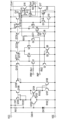
以下、本発明の実施の形態について、図1乃至図9を参照しつつ説明する。
なお、以下に説明する部材、配置等は本発明を限定するものではなく、本発明の趣旨の範囲内で種々改変することができるものである。
最初に、本発明の実施の形態における演算増幅器の基本回路構成について、図1を参照しつつ説明する。
本発明の実施の形態における演算増幅器は、差動増幅回路(図1においては「DIF1」と表記)110と、出力回路(図1においては「OST1」と表記)116に大別されて構成されたものとなっている。
DETAILED DESCRIPTION OF THE PREFERRED EMBODIMENTS Hereinafter, an embodiment of the present invention will be described with reference to FIGS.
It should be noted that the components, arrangements, etc. described below do not limit the present invention, and various modifications can be made within the scope of the present invention.
First, the basic circuit configuration of an operational amplifier according to an embodiment of the present invention will be described with reference to FIG.
The operational amplifier in the embodiment of the present invention is configured to be roughly divided into a differential amplifier circuit (denoted as “DIF1” in FIG. 1) 110 and an output circuit (denoted as “OST1” in FIG. 1) 116.
この演算増幅器の正電源端子64は、差動増幅回路110の端子D3及び出力回路116の端子D6に、それぞれ接続されている。
また、負電源端子65は、差動増幅回路110の端子D4及び出力回路116の端子D7に、それぞれ接続されている。
演算増幅器の非反転入力端子(図1においては「INP」と表記)62は、端子D2に、反転入力端子(図1においては「INM」と表記)61は、端子D1に、それぞれ接続されている。
The positive
The negative
A non-inverting input terminal (denoted as "INP" in FIG. 1) 62 of the operational amplifier is connected to a terminal D2, and an inverting input terminal (denoted as "INM" in FIG. 1) 61 is connected to a terminal D1.
さらに、演算増幅器の出力端子63は、出力回路116の端子D9に接続されている。
また、差動増幅回路110の出力端子D5は、出力回路116の入力端子D8に接続されている。
Furthermore, the
Moreover, the
差動増幅回路110は、差動対をなす2つのトランジスタなどを主たる構成要素として構成された従来から良く知られた構成を有して差動増幅を行う回路である。
かかる差動増幅回路110は、例えば、ダーリントン接続の入力差動対や、正電源電位から負電源電位までの入力信号に対応した、いわゆる入力フルスイング演算増幅器を構成するようにしても良く、特定の構成に限定される必要はない。
一方、本発明の実施の形態における出力回路116は、差動増幅回路110の出力信号を所望の電圧レベルとして出力するための従来同様の回路である。
The
Such a
On the other hand, the
この出力回路116は、過電流保護回路(図1においては「CLim」と表記)117を有している。
さらに、本発明の過電流保護回路117は、従来と異なり高周波ノイズ対策回路(図1においては「EX」と表記)122が内蔵されているが、その点を除けば基本的に従来同様の構成を有してなるものである。
この高周波ノイズ対策回路122は、過電流保護回路117が高周波成分に反応しないようにする機能を有してなるものである。すなわち、高周波ノイズ対策回路122は、高周波ノイズにより過電流保護回路117の電流リミット値が変化することのないように構成されたものである(詳細は後述)。
The
Furthermore, unlike the conventional
This high frequency
図2には、上述の基本構成における具体的な回路構成の一つである第1の回路構成例が示されており、以下、同図を参照しつつ説明する。
本発明の実施の形態における演算増幅器は、差動増幅回路110と、第1及び第2のレベルシフト回路111,112と、第3及び第4のレベルシフト回路113,114と、高利得増幅回路115と、出力回路116と、過電流保護回路117と、起動回路121と、電流源回路118と、ローパスフィルタ119とに大別されて構成されたものとなっている。
FIG. 2 shows a first example of a circuit configuration, which is one of the specific circuit configurations in the above-mentioned basic configuration, and the following description will be given with reference to this figure.
The operational amplifier in the embodiment of the present invention is broadly composed of a
本発明の実施の形態における演算増幅器は、従来の演算増幅器の回路構成と基本的に同様の回路構成を有するものであるが、電源ラインへ混入する高周波外来ノイズによる出力特性の変動を抑圧するための高周波外来ノイズ対策回路122が過電流保護回路117に設けられた構成を有する点が従来と異なるものである(詳細は後述)。
The operational amplifier in the embodiment of the present invention has a circuit configuration that is basically the same as that of a conventional operational amplifier, but differs from the conventional one in that it has a configuration in which a high-frequency external
以下、本発明の実施の形態における演算増幅器の具体的な回路構成について説明する。
まず、差動増幅回路110は、差動対を構成する第3及び第4のトランジスタ(図2においては、それぞれ「Q3」、「Q4」と表記)3,4と、アクティブ負荷を構成する第5及び第6のトランジスタ(図2においては、それぞれ「Q5」、「Q6」と表記)5,6を主たる構成要素として構成されている。
なお、本発明の実施の形態においては、第3及び第4のトランジスタ3,4にPNP型バイポーラトランジスタが、第5及び第6のトランジスタ5,6には、NPN型バイポーラトランジスタが、それぞれ用いられている。
A specific circuit configuration of the operational amplifier according to the embodiment of the present invention will now be described.
First, the
In this embodiment of the present invention, the third and
第3及び第4のトランジスタ3,4は、エミッタが相互に接続されると共に、PNP型バイポーラトランジスタを用いた第112のトランジスタ(図2においては「Q112」と表記)32のコレクタに接続されている。そして、この第112のトランジスタ32のエミッタには、正電源電圧VCCが印加されるようになっている。
The emitters of the third and
一方、第5及び第6のトランジスタ5,6は、カレントミラー接続されて設けられている。
すなわち、第5及び第6のトランジスタ5,6は、ベースが相互に接続されると共に、第5のトランジスタ5のコレクタと接続されて、第5のトランジスタ5は、いわゆるダイオード接続されて設けられている。
第5のトランジスタ5のコレクタには、第3のトランジスタ3のコレクタが、第6のトランジスタ6のコレクタには、第4のトランジスタ4のコレクタが、それぞれ接続されている。また、第5及び第6のトランジスタ5,6のエミッタには、負電源電圧VEEが印加されるようになっている。
On the other hand, the fifth and
That is, the bases of the fifth and
The collector of the
次に、第1及び第2のレベルシフト回路111,112は、反転入力端子(図2においては「INM」と表記)61と非反転入力端子(図2においては「INP」と表記)62に入力される入力信号のダイナミックレンジの下限レベルを負電源端子の電位以下に拡大する機能を果たすものである。
第1のレベルシフト回路111は、第1のトランジスタ(図2においては「Q1」と表記)1と、第111のトランジスタ(図2においては「Q111」と表記)31と、第1の入力抵抗器(図2においては「Rin1」と表記)41とを有して構成されている。
Next, the first and second
The first
また、第2のレベルシフト回路112は、第2のトランジスタ(図2においては「Q2と表記)2と、第113のトランジスタ(図2においては「Q113」と表記)33と、第2の入力抵抗器(図2においては「Rin2」と表記)42とを有して構成されている。いずれのレベルシフト回路111,112も基本的構成は同一である。
The second
なお、本発明の実施の形態においては、第1及び第2のトランジスタ1,2、並びに、第111及び第113のトランジスタ31,33には、PNP型バイポーラトランジスタが用いられている。
In this embodiment of the present invention, the first and
第1のトランジスタ1のエミッタは、第3のトランジスタ3のベースに接続されると共に、第111のトランジスタ31のコレクタに接続されている。そして、第111のトランジスタ31のエミッタには、正電源電圧VCCが印加されるようになっている。
また、第1のトランジスタ1のコレクタは、負電源電圧VEEが印加される一方、ベースは、第1の入力抵抗器41を介して反転入力端子61に接続されている。
The emitter of the
The collector of the
第2のトランジスタ2のエミッタは、第4のトランジスタ4のベースに接続されると共に、第113のトランジスタ33のコレクタに接続されている。そして、第113のトランジスタ33のエミッタには、正電源電圧VCCが印加されるようになっている。
また、第2のトランジスタ2のコレクタは、負電源電圧VEEが印加される一方、ベースは、第2の入力抵抗器42を介して非反転入力端子62に接続されている。
The emitter of the
The collector of the
第3のレベルシフト回路113は、第7のトランジスタ(図2においては「Q7」と表記)7と第110のトランジスタ(図2においては「Q110」と表記)30とを有して構成されている。この第3のレベルシフト回路113は、第5及び第6のトランジスタ5,6により構成されたアクティブ負荷に流れる電流の誤差をなくすために設けられたダミー回路である。
なお、本発明の実施の形態においては、第7のトランジスタ7及び第110のトランジスタ30に、PNP型バイポーラトランジスタが用いられている。
The third
In this embodiment of the present invention, the
第7のトランジスタ7のエミッタは、第110のトランジスタ30のコレクタに接続され、第110のトランジスタ30のエミッタには、正電源電圧VCCが印加されるようになっている。
また、第7のトランジスタ7のコレクタには、負電源電圧VEEが印加される一方、ベースは第5のトランジスタ5のコレクタに接続されている。
The emitter of the
The
第4のレベルシフト回路114は、第8のトランジスタ(図2においては「Q8」と表記)8と第114のトランジスタ34とを有して構成されている。
なお、本発明の実施の形態において、第8のトランジスタ8及び第114のトランジスタ34には、PNP型バイポーラトランジスタが用いられている。
第8のトランジスタ8のエミッタは、第114のトランジスタ34のコレクタに接続され、第114のトランジスタ34のエミッタには、正電源電圧VCCが印加されるようになっている。
The fourth
In the embodiment of the present invention, the
The emitter of the
この第4のレベルシフト回路114は、アクティブ負荷となる第6のトランジスタ6のコレクタ・エミッタ電圧を、第5のトランジスタ5のコレクタ・エミッタ間電圧Vce(=Vbe:ベース・エミッタ間電圧)と同一電位にバイアスする機能を果たす。
This fourth
高利得増幅回路115は、ダーリントン接続された第9及び第10のトランジスタ(図2においては、それぞれ「Q9」、「Q10」と表記)9,10と、第115及び第117のトランジスタ(図2においては、それぞれ「Q115」、「Q117」と表記)35,37とを有して構成されている。
本発明に実施の形態において、第9及び第10のトランジスタ9,10には、NPN型バイポーラトランジスタが、第115及び第117のトランジスタ35,37には、PNP型バイポーラトランジスタが、それぞれ用いられている。
The high
In this embodiment of the present invention, the ninth and
第9のトランジスタ9のベースは、第8のトランジスタ8のエミッタに接続される一方、エミッタは、第10のトランジスタ10のベースに接続されている。
また、第9のトランジスタ9のコレクタは、第115のトランジスタ35のコレクタに接続されており、この第115のトランジスタ35のエミッタには、正電源電圧VCCが印加されるようになっている。
The base of the
The collector of the
一方、第10のトランジスタ10のコレクタは、第117のトランジスタ37のコレクタに接続されており、この第117のトランジスタ37のエミッタには、正電源電圧VCCが印加されるようになっている。
また、第10のトランジスタ10のエミッタは、負電源電圧VEEが印加されるようになっている。
そして、第10のトランジスタ10のコレクタは、次述する出力回路116の入力段に接続されている。
On the other hand, the collector of the
The emitter of the
The collector of the
出力回路116は、第15乃至第17のトランジスタ(図2においては、それぞれ「Q15」、「Q16」、「Q17」と表記)15~17と、第1及び第2の抵抗器(図2においては、それぞれ「R1」、「R2」と表記)43,44とを有して構成されている。
本発明の実施の形態において、第15及び第16のトランジスタ15,16には、NPN型バイポーラトランジスタが、第17のトランジスタ17には、PNP型バイポーラトランジスタが、それぞれ用いられている。
The
In the embodiment of the present invention, the fifteenth and
正電源電圧VCCと負電源電圧VEEとの間に、正電源電圧VCC側から、第16のトランジスタ16、第2の抵抗器44、及び、第17のトランジスタ17が直列接続されて設けられている。
第16のトランジスタ16のベースには、この第16のトランジスタ16とダーリントン回路を構成する第15のトランジスタ15のエミッタが接続されると共に、第1の抵抗器43を介して第16のトランジスタ16のエミッタが接続されている。
Between the positive power supply voltage VCC and the negative power supply voltage VEE, a
The base of the
第15のトランジスタ15のコレクタには、正電源電圧VCCが印加されるようになっている一方、ベースは、高利得増幅回路115の第10のトランジスタ10のコレクタに接続されている。
なお、第15のトランジスタ15のベースと第8のトランジスタ8のベースとの間には、第15のトランジスタ15のベース側から、減衰抵抗器(図2においては「RX11」と表記)49、位相補償用コンデンサ(図2においては「C1」と表記)51の順で直列接続されて設けられている。
The collector of the
Between the base of the
過電流保護回路117は、第11乃至第14のトランジスタ(図2においては、それぞれ「Q11」、「Q12」、「Q13」、「Q14」と表記)11~14と、第116のトランジスタ(図2においては「Q116」と表記)36とを有して構成されている。かかる過電流保護回路117は、出力回路116の第16のトランジスタ16に流れる電流の抑圧と、第9のトランジスタ9のコレクタ電流の制限を行うものである。本発明の実施の形態においては、出力段に設けられた第2の抵抗器44が、過電流保護回路117の検出用抵抗器として流用される構成となっている。
なお、本発明の実施の形態において、第11及び第116のトランジスタ11,36には、PNP型バイポーラトランジスタが、第12乃至第14のトランジスタ12~14には、NPN型バイポーラトランジスタが、それぞれ用いられている。
The
In the embodiment of the present invention, the eleventh and
第12及び第13のトランジスタ12,13は、カレントミラー回路を構成している。
すなわち、第12及び第13のトランジスタ12,13のベースは相互に接続されると共に、第12のトランジスタ12のコレクタに接続されている一方、各々のエミッタには、負電源電圧VEEが印加されるようになっている。
The twelfth and
That is, the bases of the twelfth and
また、第12のトランジスタ12のコレクタは、第116のトランジスタ36のコレクタに接続され、第116のトランジスタ36のエミッタには、正電源電圧VCCが印加されるようになっている。さらに、第12のトランジスタ12のコレクタには、第11のトランジスタ11のベースが接続されている。
第11のトランジスタ11のエミッタは、第9のトランジスタ9のコレクタに接続される一方、第11のトランジスタ11のコレクタには、負電源電圧VEEが印加されるようになっている。
The collector of the
The emitter of the
また、第13のトランジスタ13のコレクタは、過電流検出用トランジスタである第14のトランジスタ14のベースと共に第16のトランジスタ16のエミッタに接続されている。
そして、第14のトランジスタ14のコレクタは、第15のトランジスタ15のベースに接続される一方、第14のトランジスタ14のエミッタは、第17のトランジスタ17のエミッタと共に出力端子63に接続されている。
The collector of the
The collector of the
本発明の実施の形態における過電流保護回路117には、従来と異なり、次述するように高周波ノイズ対策回路122が設けられている。
すなわち、高周波ノイズ対策回路122は、第1のノイズ対策コンデンサ(図2においては「CX2」と表記)53と、第2の抵抗器44とを有して構成されている。
第1のノイズ対策コンデンサ53と第2の抵抗器44は、並列接続状態とされて、その一端は第16のトランジスタ16のエミッタに、他端は出力端子63に、それぞれ接続されている。
Unlike the conventional
That is, the high frequency
The first
電流源回路118は、第109乃至第117のトランジスタ(図2においては、それぞれ「Q109」、「Q110」、「Q111」、「Q112」、「Q113」、「Q114」、「Q115」、「Q116」、「Q117」と表記)29~37と、定電流源回路120とを有して構成されている。
本発明の実施の形態において、第109乃至第117のトランジスタ29~37には、PNP型バイポーラトランジスタが用いられている。
The
In the embodiment of the present invention, the 109th to
第109のトランジスタ29と、第110乃至第117のトランジスタ30~37は、カレントミラー回路を構成しており、入力段を構成する第109のトランジスタ29側から出力段となる第110乃至第117のトランジスタ30~37の各トランジスタに電流出力が得られるようになっている。
すなわち、第109のトランジスタ29のエミッタには、正電源電圧VCCが印加されるようになっている一方、ベースとコレクタとは相互に接続されて、その接続点と負電源電圧VEEとの間に定電流源120が設けられている。
そして、第109のトランジスタ29のベースは、第110乃至第117のトランジスタ30~37の各ベースと相互に接続されている。
The
That is, the positive power supply voltage VCC is applied to the emitter of the
The base of the
定電流源回路120は、第103乃至第108のトランジスタ(図2においては、それぞれ「Q103」、「Q104」、「Q105」、「Q106」、「Q107」、「Q108」と表記)23~28と、電流源用第1乃至第3の抵抗器(図2においては、それぞれ「R101」、「R102」、「R103」と表記)46~48を有して構成されている。
The constant
この第1の回路構成例において、第103及び第104のトランジスタ23,24、並びに第107及び第108のトランジスタ27,28には、NPN型バイポーラトランジスタが、第105及び第106のトランジスタ25,26には、PNP型バイポーラトランジスタが、それぞれ用いられている。
In this first circuit configuration example, NPN-type bipolar transistors are used for the 103rd and
第103のトランジスタ23は、第102のトランジスタ22と相互のコレクタ同士、相互のエミッタ同士が、それぞれ接続されており、エミッタ同士の接続点と負電源端子65との間には電流源用第2の抵抗器47が接続されている。
第102及び第103のトランジスタ22,23のコレクタ同士の接続点は、第105のトランジスタ25のベースに接続されると共に、電流源用第1の抵抗器46を介して第105のトランジスタ25のコレクタ及び第106のトランジスタ26のベースに接続されている。
The
The connection point between the collectors of the 102nd and
第105及び第106のトランジスタ25,26のエミッタは、共に正電源端子64に接続されている。
また、第103のトランジスタ23のベースは、第104のトランジスタ24のベースと相互に接続されると共に、第104のトランジスタ24のコレクタに接続されている。そして、第103のトランジスタ23と第104のトランジスタ24は、カレントミラー回路を構成している。
The emitters of the 105th and
In addition, the base of the
第104のトランジスタ24のコレクタは、第106のトランジスタ26のコレクタに接続される一方、第104のトランジスタ24のエミッタは、電流源用第3の抵抗器48を介して第107のトランジスタ27のコレクタに接続されている。
また、第107のトランジスタ27のベースは、第104のトランジスタ24のエミッタに接続され、第107のトランジスタ27のコレクタには、第108のトランジスタ28のベースが接続されている。
The collector of the
The base of the 107th transistor 27 is connected to the emitter of the
第107及び第108のトランジスタ27,28のエミッタは、共に負電源端子65に接続される一方、第108のトランジスタ28のコレクタは、第109のトランジスタ29のコレクタ及びベースに接続されている。
第109のトランジスタ29のエミッタは、正電源端子64に接続されている。この第109のトランジスタ29は、第110乃至第117のトランジスタ30~37と共にカレントミラー回路を構成している。
The emitters of the 107th and
The emitter of the
次に、起動回路121は、起動用ダイオード(フィルタ用ダイオード)55と、起動用抵抗器(フィルタ用抵抗器)56と、第102のトランジスタ(図2においては「Q102」と表記)22とを有して構成されている。
起動用ダイオード(図2においては「DX1」と表記)55のアノードは、起動用抵抗器(図2においては「RX1」と表記)56を介して正電源端子64に接続される一方、カソードは、負電源端子65に接続されている。
また、起動用ダイオード55のアノードには、第102のトランジスタ(起動用トランジスタ)22のベースが接続されている。
なお、第102のトランジスタ22には、NPN型バイポーラトランジスタが用いられている。
Next, the
The anode of the start-up diode (labeled “DX1” in FIG. 2 ) 55 is connected to the positive
The anode of the
The
ローパスフィルタ119は、フィルタ用抵抗器を兼ねる起動用抵抗器56と、フィルタ用ダイオードを兼ねる起動用ダイオード55と、フィルタ用コンデンサ(図2においては「CX1」と表記)52とを有して構成されており、起動回路121の起動用抵抗器56と起動用ダイオード55を流用する構成となっている。
The low-
次に、過電流保護回路117の動作について説明する。
ここでは、高周波外来ノイズの電源ラインへの混入が無い正常時における動作について説明する。
高周波外来ノイズの電源ラインへの混入が無い正常における過電流保護回路117の動作は、従来同様であるので、以下、概括的に説明する。
過電流保護回路117は、第2の抵抗器44に流れる電流Ioutが下記する式2の条件を満たすまで増加した際にON状態となる。
Next, the operation of the
Here, the operation under normal conditions when no high frequency external noise is mixed into the power supply line will be described.
The operation of the
The
Vbe(Q14)=R2×Iout・・・式2
Vbe(Q14)=R2×Iout...
ここで、Vbe(Q14)は、過電流検出用トランジスタである第14のトランジスタ14のベース・エミッタ間電圧であって、具体的には、約0.6Vである。
また、R2は、第2の抵抗器44の抵抗値、Ioutは、第2の抵抗器44を流れる出力電流の電流値である。
出力電流Ioutが増加し、式2の条件を満たす状態となった際に、第14のトランジスタ14のコレクタ電流IcQ14が流れ、第15のトランジスタ15のベース電流IbQ15が制限されることとなる。
Here, Vbe(Q14) is the base-emitter voltage of the
Furthermore, R2 is the resistance value of the
When the output current Iout increases and satisfies the condition of the
その結果、第15のトランジスタ15とダーリントン接続された第16のトラジスタ16のエミッタ電流は、式2を満たす出力電流Ioutを越える大きな電流を流せなくなり、過電流保護が図られることとなる。
かかる動作を有する過電流保護回路117の回路構成は、フィードバック回路が構成されたものとなっている。
As a result, the emitter current of the
The circuit configuration of the
次に、高周波ノイズ対策回路122を構成する第1のノイズ対策コンデンサ53の容量値CX2の選定について説明する。
第1のノイズ対策コンデンサ53の容量値CX2は、下記する式3の条件を満たすものを選択するのが好適である。
Next, the selection of the capacitance value CX2 of the first
It is preferable to select the capacitance value CX2 of the first
CX2>1/(2π×21/2×fc×R2)・・・式3
CX2>1/(2π×2 1/2 ×fc×R2)...
ここで、CX2は第1のノイズ対策コンデンサ53の容量値、fcは除去する高周波ノイズの周波数、R2は第2の抵抗器44の抵抗値である。
かかる容量値の第1のノイズ対策コンデンサ53を用いることで、過電流保護回路117の検出抵抗のインピーダンスZが引き下げられ、高周波領域での過電流保護回路117の過電流検出の感度が低下し、動作し難くなる。そのため、高周波ノイズの混入に起因して過電流保護回路117が安易に動作することがなく、従来と異なり、出力電流の不用意な低下を招くようなことが抑圧、防止されることとなる。
上述のインピーダンスZは、下記する式4で表される。
Here, CX2 is the capacitance value of the first
By using the first
The above-mentioned impedance Z is expressed by the
Z=1/{(1/R2)2+(2π・fc・CX2)2}1/2・・・式4
Z=1/{(1/R2) 2 + (2π・fc・CX2) 2 } 1/2 ...
ここで、Zは過電流保護回路117の検出抵抗の合成インピーダンスの大きさ、R2は第2の抵抗器44の抵抗値、fcは除去を望む高周波ノイズの周波数、CX2は第1のノイズ対策コンデンサ53の容量値である。なお、過電流保護回路117の検出抵抗は、第2の抵抗器44と第1のノイズ対策コンデンサ53との並列接続部分を意味する。
Here, Z is the magnitude of the composite impedance of the detection resistor of the
図5には、第2の抵抗器44の抵抗値を一定の値とし、第1のノイズ対策コンデンサ53の容量値を種々変えた場合の式4で示される検出抵抗の合成インピーダンスZの周波数変化に対する変化特性例が示されており、以下、同図について説明する。
図5においては、第2の抵抗器44の抵抗値を15Ωとした場合に、第1のノイズ対策コンデンサ53の容量値CX2を、CX2=5pF、CX2=10pF、CX2=15pFとした場合の、それぞれの合成インピーダンスZの周波数変化を示す特性線が示されている。
FIG. 5 shows an example of the change characteristic of the synthetic impedance Z of the detection resistor, as shown in
FIG. 5 shows characteristic lines indicating the frequency change of the synthetic impedance Z when the resistance value of the
いずれの場合も、遮断、低減の対象とする高周波ノイズの周波数が高くなるにつれて、インピーダンスZが容量値に応じた変化率で低下してゆくものとなっていることが確認できる。
したがって、このような容量値と合成インピーダンスZとの相関関係を考慮しつつ、遮断の対象とする高周波ノイズ周波数に応じて、第1のノイズ対策コンデンサ53の容量値を適宜選定することが重要となる。
In either case, it can be seen that as the frequency of the high-frequency noise to be blocked or reduced increases, the impedance Z decreases at a rate that corresponds to the capacitance value.
Therefore, it is important to appropriately select the capacitance value of the first
図6には、図2に示された回路構成において、第1のノイズ対策コンデンサ53の容量値CX2を14pFとし、先に図15に示された検証回路を用いて計測された電源ラインへのAC入力電力の変化に対する出力電圧Voutの変化特性例が示されており、以下、同図について説明する。
Figure 6 shows an example of the change characteristics of the output voltage Vout relative to the change in AC input power to the power line measured using the verification circuit previously shown in Figure 15 when the capacitance value CX2 of the first
図6において、第1の回路構成(実施例1)の特性例が実線の特性線により、従来回路(図17参照)の特性例が点線の特性線により、それぞれ示されている。
なお、AC電圧源RFの出力周波数は0.61GHzである。
In FIG. 6, a characteristic example of the first circuit configuration (Example 1) is shown by a solid characteristic line, and a characteristic example of the conventional circuit (see FIG. 17) is shown by a dotted characteristic line.
The output frequency of the AC voltage source RF is 0.61 GHz.
従来回路の場合、AC電圧源RFの入力電力PinがPin=29dBmまでしか出力電圧Voutを一定保つことができなかった(図6の点線の特性線参照)。
これに対して、第1の回路構成(実施例1)にあっては、入力電力PinがPin=31dBmまで出力電圧Voutを一定値6Vに保つことができるものとなっていることが確認できる(図6の実線の特性線参照)。
In the case of the conventional circuit, the output voltage Vout could only be kept constant up to an input power Pin of the AC voltage source RF of Pin=29 dBm (see the dotted characteristic line in FIG. 6).
In contrast, in the first circuit configuration (Example 1), it can be confirmed that the output voltage Vout can be maintained at a constant value of 6 V up to an input power Pin of Pin = 31 dBm (see the solid characteristic line in Figure 6).
このような顕著な効果は、先に述べたように、第1のノイズ対策コンデンサ53と第2の抵抗器44とを並列接続状態で設けることで、過電流保護回路117の高周波領域での合成インピーダンスを低下させ、高周波領域で過電流保護回路117を動作し難くしたことによるものである。
一方、直流レベルでの過電流保護回路117の電流リミット値Ioutrは、第1のノイズ対策コンデンサ53を設ける以前と変わらない。
ここで、電流リミット値Ioutrは、過電流保護回路117が第2の抵抗器44に流れる電流が過電流であるとする際の電流値である。
As mentioned above, this remarkable effect is achieved by connecting the first
On the other hand, the current limit value Ioutr of the
Here, the current limit value Ioutr is a current value when the
図9には、回路構成毎の電流リミット値を説明する説明図が示されているが、同図によれば、上述した第1の回路構成(実施例1)、また、後述する第2及び第3(実施例2及び実施例3)の回路構成、さらに、従来回路のいずれにおいても電流リミット値は変わらないことが確認できる。なお、図9における従来回路は、図17に示された回路構成のものである。
このように電流リミット値が変わらないのは、直流レベルでは第1のノイズ対策コンデンサ53のインピーダンスは無限大と近似できるためである。
過電流保護回路117の電流リミット値Ioutrが変わらないことで、出力電流Ioutを所望の電流値以下に抑制することができ、過電流による回路焼損などのクリティカルな問題発生を防止することが可能となる。
9 shows an explanatory diagram for explaining the current limit value for each circuit configuration, and according to this diagram, it can be confirmed that the current limit value is the same in the first circuit configuration (Example 1) described above, the second and third circuit configurations (Examples 2 and 3) described below, and the conventional circuit. Note that the conventional circuit in FIG. 9 has the circuit configuration shown in FIG.
The current limit value does not change because the impedance of the first
Since the current limit value Ioutr of the
したがって、本発明の実施の形態の回路構成を採ることで、高周波ノイズ対策に起因して直流レベルでの過電流保護回路117の電流リミット値を変化させることなく、電源ラインに混入する高周波ノイズに対して出力電圧の変動を抑制する演算増幅器を提供することが可能となる。
Therefore, by adopting the circuit configuration of the embodiment of the present invention, it is possible to provide an operational amplifier that suppresses fluctuations in the output voltage due to high-frequency noise that is mixed into the power line, without changing the current limit value of the
なお、この第1の回路構成例において、第1のノイズ対策コンデンサ53を、第14のトランジスタ14のベース・エミッタ間のPN接合により生ずる寄生容量に代替させても良い。この場合、第1のノイズ対策コンデンサ53の素子面積を確保する必要がなくなるため、チップ面積の縮小化を図ることが可能となる。
In addition, in this first circuit configuration example, the first
次に、第2の回路構成例について、図3を参照しつつ説明する。
なお、図1に示された第1の回路構成例における構成要素と同一の構成要素については同一の符号を付して、その詳細な説明を省略し、以下、異なる点を中心に説明する。
この第2の回路構成例は、次述する構成の高周波ノイズ対策回路122Aが設けられたものである。この高周波ノイズ対策回路122Aは、ノイズ対策抵抗器(図3においては「RX2」と表記)57と第2のノイズ対策コンデンサ(図3においては「CX3」と表記)54とを有して次述するように構成されたものとなっている。
Next, a second circuit configuration example will be described with reference to FIG.
The same components as those in the first circuit configuration example shown in FIG. 1 are denoted by the same reference numerals, and detailed description thereof will be omitted. The following description will focus on the differences.
The second circuit configuration example is provided with a high-frequency noise countermeasure circuit 122A having the following configuration. The high-frequency noise countermeasure circuit 122A has a noise countermeasure resistor (indicated as "RX2" in FIG. 3) 57 and a second noise countermeasure capacitor (indicated as "CX3" in FIG. 3) 54, and is configured as described below.
ノイズ対策抵抗器57は、その一端が第14のトランジスタ14のベースに接続され、他端は第16のトランジスタ16のエミッタ、換言すれば、第16のトランジスタ16のエミッタと第2の抵抗器44との接続点に接続されている。
また、第2のノイズ対策コンデンサ54は、その一端が第14のトランジスタ14のベースに、他端が第14のトランジスタ14のエミッタに、それぞれ接続されたものとなっている。
The
The second noise suppression capacitor 54 has one end connected to the base of the
次に、かかる構成における動作等について説明する。
この第2の回路構成は、過電流保護回路117において、第2の抵抗器44を介して出力電流値の検出を行う第14のトランジスタ14のベースとエミッタ間の電圧に、ノイズ対策抵抗器57と第2のノイズ対策コンデンサ54によるローパスフィルタによるフィルタリングが施されるものとなっている。
Next, the operation of such a configuration will be described.
In this second circuit configuration, in the
ノイズ対策抵抗器57と第2のノイズ対策コンデンサ54の各々の大きさは、下記する式5の条件を満たすものとする。
The size of each of the
fc>1/(2π×CX3×RX2)・・・式5
fc>1/(2π×CX3×RX2)...
ここで、fcは除去する高周波ノイズの周波数、CX3は第2のノイズ対策コンデンサ54の容量値、RX2はノイズ対策抵抗器57の抵抗値である。
Here, fc is the frequency of the high-frequency noise to be removed, CX3 is the capacitance value of the second noise suppression capacitor 54, and RX2 is the resistance value of the
図7には、図3に示された回路構成において、ノイズ対策抵抗器57の抵抗値RX2をRX2=1KΩ、第2のノイズ対策コンデンサ54の容量値CX3をCX3=4pFとし、先に図15に示された検証回路を用いて計測された電源ラインへのAC入力電力の変化に対する出力電圧Voutの変化特性例が示されており、以下、同図について説明する。
Figure 7 shows an example of the change characteristics of the output voltage Vout relative to the change in AC input power to the power line measured using the verification circuit previously shown in Figure 15 when the resistance value RX2 of the
図7において、第2の回路構成(実施例2)の特性例が実線の特性線により、従来回路(図17参照)の特性例が点線の特性線により、それぞれ示されている。
なお、AC電圧源RFの出力周波数は0.61GHzである。
In FIG. 7, a characteristic example of the second circuit configuration (embodiment 2) is shown by a solid characteristic line, and a characteristic example of the conventional circuit (see FIG. 17) is shown by a dotted characteristic line.
The output frequency of the AC voltage source RF is 0.61 GHz.
従来回路の場合、AC電圧源RFの入力電力PinがPin=29dBmまでしか出力電圧Voutを一定保つことができなかった(図7の点線の特性線参照)。
これに対して、第2の回路構成(実施例2)にあっては、入力電力PinがPin=32dBmまで出力電圧Voutを一定値6Vに保つことができるものとなっていることが確認できる(図7の実線の特性線参照)。
In the case of the conventional circuit, the output voltage Vout could only be kept constant up to an input power Pin of the AC voltage source RF of Pin=29 dBm (see the dotted characteristic line in FIG. 7).
In contrast, in the second circuit configuration (Example 2), it can be confirmed that the output voltage Vout can be maintained at a constant value of 6 V up to an input power Pin of Pin = 32 dBm (see the solid characteristic line in Figure 7).
このような顕著な効果が生ずるのは、先に述べたように、第2のノイズ対策コンデンサ54とノイズ対策抵抗器57とを設けることで、第14のトランジスタ14のベース・エミッタ間の電圧に対して、第2のノイズ対策コンデンサ54とノイズ対策抵抗器57とによるローパスフィルタによるフィルタリング(ローパスフィルタ作用)が施されることとなるためである。すなわち、上述のローパスフィルタ作用により、第14のトランジスタ14が高周波信号に対して反応し難くなり、高周波領域で過電流保護回路117が動作し難くなる、すなわち、換言すれば、高周波領域での過電流保護回路117の過電流検出感度が低下するためである。
The reason why such a remarkable effect is produced is that, as mentioned above, by providing the second noise suppression capacitor 54 and the
一方、直流レベルでの過電流保護回路117の電流リミット値Ioutrは、第2のノイズ対策コンデンサ54及びノイズ対策抵抗器57を設ける以前と変わらない(図9参照)。
したがって、この第2の回路構成にあっても、第1の回路構成と同様に、高周波ノイズ対策に起因して直流レベルでの過電流保護回路117の電流リミット値を変化させることなく、電源ラインに混入する高周波ノイズに対して出力電圧の変動を抑制する演算増幅器を提供することが可能となる。
On the other hand, the current limit value Ioutr of the
Therefore, with this second circuit configuration, as with the first circuit configuration, it is possible to provide an operational amplifier that suppresses fluctuations in output voltage due to high-frequency noise that is mixed into the power supply line, without changing the current limit value of
なお、第2のノイズ対策コンデンサ54を設けることに代えて、第14のトランジスタ14のベース・エミッタ間のPN接合により生ずる寄生容量に代替させても良い。この場合、第2のノイズ対策コンデンサ54の素子面積を確保する必要がなくなるため、チップ面積の縮小化を図ることが可能となる。
In addition, instead of providing the second noise suppression capacitor 54, a parasitic capacitance generated by the PN junction between the base and emitter of the
次に、第3の回路構成例について、図4を参照しつつ説明する。
なお、図1、図2又は図3に示された回路構成例における構成要素と同一の構成要素については同一の符号を付して、その詳細な説明を省略し、以下、異なる点を中心に説明する。
この第3の回路構成例は、図2に示された第1の回路構成における高周波ノイズ対策回路122の構成と図3に示された第2の回路構成における高周波ノイズ対策回路122Aの構成の双方を備えたものである。
Next, a third circuit configuration example will be described with reference to FIG.
The same components as those in the circuit configuration example shown in FIG. 1, FIG. 2 or FIG. 3 are denoted by the same reference numerals, and detailed description thereof will be omitted. The following description will focus on the differences.
This third circuit configuration example has both the configuration of the high frequency
すなわち、第3の回路構成例における高周波対策回路122Bは、第2の抵抗器44と、第1のノイズ対策コンデンサ53と、ノイズ対策抵抗器57と、第2のノイズ対策コンデンサ54とを有して構成されたものとなっている。
以下、具体的に説明すれば、まず、第2の抵抗器44は、第16のトランジスタ16のエミッタと第17のトランジスタ17のエミッタ間に直列接続されて設けられて、この第2の抵抗器44と第1のノイズ対策コンデンサ53が並列接続されている点は、基本的に第1の回路構成で説明した構成と同一である。
かかる構成により、第14のトランジスタ14における検出抵抗の合成インピーダンスは、第1の回路構成と同様に引き下げられ、高周波領域で過電流保護回路117が動作し難くなる。
That is, the high frequency countermeasure circuit 122B in the third circuit configuration example is configured to include a
To explain in more detail below, first, the
With this configuration, the composite impedance of the detection resistor in the
また、ノイズ対策抵抗器57が第14のトランジスタ14のベースと第16のトランジスタ16のエミッタ間に直列接続されて設けられ、第2のノイズ対策コンデンサ54が第14のトランジスタ14のベースとエミッタ間に接続されてローパスフィルタとして機能する点も、基本的に第2の回路構成で説明した構成と同一である。
In addition, a
したがって、第2の回路構成同様、第14のトランジスタ14のベースとエミッタ間の電圧に対するローパスフィルタ作用により、高周波領域で過電流保護回路117が動作し難くなる。
この第3の回路構成例は、ローパスフィルタ作用と、第14のトランジスタ14の検出抵抗の合成インピーダンスの低下の2つのが機能するため、第1の回路構成、又は、第2の回路構成のいずれかを採る場合に比して、より高い高周波外来ノイズ耐性を確保可能となっている。
Therefore, similarly to the second circuit configuration, the low-pass filter effect on the voltage between the base and emitter of the
This third circuit configuration example has two functions: a low-pass filter action and a reduction in the synthetic impedance of the detection resistor of the
図8には、この第3の回路構成における演算増幅器の電源ラインへのAC入力電力の変化に対する出力電圧Voutの変化特性例が示されており、以下、同図について説明する。
図8に示された特性例は、ノイズ対策抵抗器57の抵抗値RX2をRX2=1KΩ、第1のノイズ対策コンデンサ53の容量値CX2をCX2=14pF、第2のノイズ対策コンデンサ54の容量値CX3をCX3=4pFとし、先に図15に示された検証回路を用いて計測されたものである。
FIG. 8 shows an example of the change characteristics of the output voltage Vout relative to the change in AC input power to the power supply line of the operational amplifier in this third circuit configuration, and this figure will be described below.
The example characteristics shown in FIG. 8 were measured using the verification circuit previously shown in FIG. 15, with the resistance value RX2 of the
図8において、第3の回路構成(実施例3)の特性例が実線の特性線により、従来回路(図17参照)の特性例が点線の特性線により、それぞれ示されている。
いずれの特性例も、AC電圧源RFの出力周波数は0.61GHzで、AC電圧源RFの入力電力Pinを変化させた場合の出力電圧Voutの変動特性を示したものである。
In FIG. 8, a characteristic example of the third circuit configuration (embodiment 3) is shown by a solid characteristic line, and a characteristic example of the conventional circuit (see FIG. 17) is shown by a dotted characteristic line.
In each of the characteristic examples, the output frequency of the AC voltage source RF is 0.61 GHz, and the fluctuation characteristic of the output voltage Vout is shown when the input power Pin of the AC voltage source RF is changed.
従来回路の場合、RF入力電力PinがPin=29dBmまでしか出力電圧Voutを一定保つことができなかった(図8の点線の特性線参照)。
これに対して、第3の回路構成(実施例3)にあっては、RF入力電力PinがPin=33dBmまで出力電圧Voutを一定値6Vに保つことができるものとなっていることが確認できる(図8の実線の特性線参照)。
一方、直流レベルでの過電流保護回路117の電流リミット値Ioutrは、ノイズ対策抵抗器57、第1及び第2のノイズ対策コンデンサ53,54を設ける以前と変わらない(図9参照)。この図9の測定例の場合、電流リミット値Ioutrは45mAで一定している。
In the case of the conventional circuit, the output voltage Vout could only be kept constant up to an RF input power Pin of 29 dBm (see the dotted characteristic line in FIG. 8).
In contrast, in the third circuit configuration (Example 3), it can be confirmed that the output voltage Vout can be maintained at a constant value of 6 V up to an RF input power Pin of Pin = 33 dBm (see the solid characteristic line in Figure 8).
On the other hand, the current limit value Ioutr of the
なお、この第3の回路構成例においても、先の第2の回路構成例の場合と同様、第2のノイズ対策コンデンサ54を、第14のトランジスタ14のベース・エミッタ間のPN接合により生ずる寄生容量に代替させても良い。
In addition, in this third circuit configuration example, as in the second circuit configuration example, the second noise suppression capacitor 54 may be replaced with a parasitic capacitance generated by the PN junction between the base and emitter of the
過電流保護回路の出力電流値の不要な増加を招くことなく、電源ラインへの高周波外来ノイズの混入に対して安定した出力特性が所望される演算増幅器に適用できる。 This can be applied to operational amplifiers where stable output characteristics against high-frequency external noise entering the power supply line are required, without causing an unnecessary increase in the output current value of the overcurrent protection circuit.
44…第2の抵抗器
53…第1のノイズ対策コンデンサ
54…第2のノイズ対策コンデンサ
57…ノイズ対策抵抗器
117…過電流保護回路
122…高周波ノイズ対策回路
44...
Claims (5)
前記演算増幅器は、出力段における過電流が検出された場合に前記出力段の電流抑圧を可能としてなる過電流保護回路を有し、前記過電流保護回路は、所望の高周波領域における過電流検出の感度を抑制する高周波ノイズ対策回路が設けられてなり、
前記過電流保護回路は、過電流検出用トランジスタと、前記出力段に流れる電流検出のために前記出力段に設けられた検出用抵抗器とを有し、前記過電流検出用トランジスタのベースとエミッタ間に前記検出用抵抗器が接続されて、前記検出用抵抗器における過電流が検出された場合に前記過電流検出用トランジスタにより前記出力段の電流を低減するよう構成されてなり、
前記高周波ノイズ対策回路は、前記検出用抵抗器と並列接続された第1のノイズ対策コンデンサを有してなり、
前記第1のノイズ対策コンデンサの容量値CX2は、
不等式CX2>1/(2π×21/2×fc×R2)を満たす値に設定され、
前記不等式におけるfcは、除去する高周波ノイズの周波数、前記不等式におけるR2は、前記検出用抵抗器の抵抗値であり、
前記検出用抵抗器と前記第1のノイズ対策コンデンサとの並列接続部分におけるインピーダンスの低下により前記過電流保護回路における前記高周波領域での過電流検出感度を低下せしめることで前記高周波ノイズに起因する出力電圧の変動抑圧を図ったことを特徴とする演算増幅器。 An operational amplifier configured to be capable of differentially amplifying an input signal applied between a non-inverting input terminal and an inverting input terminal,
the operational amplifier has an overcurrent protection circuit capable of suppressing a current in an output stage when an overcurrent is detected in the output stage, the overcurrent protection circuit being provided with a high-frequency noise suppression circuit for suppressing sensitivity of overcurrent detection in a desired high-frequency region;
the overcurrent protection circuit includes an overcurrent detection transistor and a detection resistor provided in the output stage for detecting a current flowing through the output stage, the detection resistor is connected between a base and an emitter of the overcurrent detection transistor, and when an overcurrent is detected in the detection resistor, the overcurrent detection transistor reduces a current in the output stage;
the high frequency noise countermeasure circuit includes a first noise countermeasure capacitor connected in parallel with the detection resistor,
The capacitance value CX2 of the first noise suppression capacitor is
It is set to a value that satisfies the inequality CX2>1/(2π×2 1/2 ×fc×R2),
In the inequality, fc is the frequency of the high-frequency noise to be removed, and R2 in the inequality is the resistance value of the detection resistor,
An operational amplifier characterized in that the impedance at the parallel connection portion of the detection resistor and the first noise suppression capacitor is reduced, thereby reducing the overcurrent detection sensitivity in the high frequency range in the overcurrent protection circuit, thereby suppressing fluctuations in output voltage caused by the high frequency noise.
前記ノイズ対策抵抗器の抵抗値RX2と前記第2のノイズ対策コンデンサの容量値CX3は、
不等式fc>1/(2π×CX3×RX2)を満たす値に設定され、
前記ノイズ対策抵抗器と前記第2のノイズ対策コンデンサによるローパスフィルタ作用により前記過電流保護回路における高周波領域での過電流検出感度を低下せしめることで前記高周波ノイズに起因する出力電圧の変動抑圧を図ったことを特徴とする請求項1記載の演算増幅器。 a noise countermeasure resistor is connected between the detection resistor and the base of the overcurrent detection transistor, and a second noise countermeasure capacitor is connected between the base and emitter of the overcurrent detection transistor in place of the first noise countermeasure capacitor;
The resistance value RX2 of the noise countermeasure resistor and the capacitance value CX3 of the second noise countermeasure capacitor are
It is set to a value that satisfies the inequality fc>1/(2π×CX3×RX2),
2. The operational amplifier according to claim 1, characterized in that the low-pass filter action of the noise suppression resistor and the second noise suppression capacitor reduces the overcurrent detection sensitivity in the high frequency range in the overcurrent protection circuit, thereby suppressing fluctuations in the output voltage caused by the high frequency noise.
前記ノイズ対策抵抗器の抵抗値RX2と前記第2のノイズ対策コンデンサの容量値CX3は、
不等式fc>1/(2π×CX3×RX2)を満たす値に設定され、
前記検出用抵抗器と前記第1のノイズ対策コンデンサとの並列接続部分におけるインピーダンスの低下による前記高周波ノイズに起因する出力電圧の変動抑圧に加えて、
前記ノイズ対策抵抗器と前記第2のノイズ対策コンデンサによるローパスフィルタ作用により前記過電流保護回路における高周波領域での過電流検出感度を低下せしめることで前記高周波ノイズに起因する出力電圧の変動抑圧を図ったことを特徴とする請求項1記載の演算増幅器。 A noise countermeasure resistor is provided between the base of the overcurrent detection transistor and the detection resistor, and a second noise countermeasure capacitor is provided between the base and emitter of the overcurrent detection transistor. A resistance value RX2 of the noise countermeasure resistor and a capacitance value CX3 of the second noise countermeasure capacitor are expressed as follows:
It is set to a value that satisfies the inequality fc>1/(2π×CX3×RX2),
In addition to suppressing the fluctuation of the output voltage caused by the high frequency noise by reducing the impedance at the parallel connection portion of the detection resistor and the first noise suppression capacitor,
2. The operational amplifier according to claim 1, characterized in that the low-pass filter action of the noise suppression resistor and the second noise suppression capacitor reduces the overcurrent detection sensitivity in the high frequency range in the overcurrent protection circuit, thereby suppressing fluctuations in the output voltage caused by the high frequency noise.
Priority Applications (1)
| Application Number | Priority Date | Filing Date | Title |
|---|---|---|---|
| JP2020142809A JP7554075B2 (en) | 2020-08-26 | 2020-08-26 | Operational Amplifier |
Applications Claiming Priority (1)
| Application Number | Priority Date | Filing Date | Title |
|---|---|---|---|
| JP2020142809A JP7554075B2 (en) | 2020-08-26 | 2020-08-26 | Operational Amplifier |
Publications (2)
| Publication Number | Publication Date |
|---|---|
| JP2022038352A JP2022038352A (en) | 2022-03-10 |
| JP7554075B2 true JP7554075B2 (en) | 2024-09-19 |
Family
ID=80499003
Family Applications (1)
| Application Number | Title | Priority Date | Filing Date |
|---|---|---|---|
| JP2020142809A Active JP7554075B2 (en) | 2020-08-26 | 2020-08-26 | Operational Amplifier |
Country Status (1)
| Country | Link |
|---|---|
| JP (1) | JP7554075B2 (en) |
Citations (3)
| Publication number | Priority date | Publication date | Assignee | Title |
|---|---|---|---|---|
| JP2001230639A (en) | 2000-02-18 | 2001-08-24 | Hitachi Ltd | Differential amplifier circuit |
| JP2002291237A (en) | 2001-03-28 | 2002-10-04 | Fujitsu Denso Ltd | Overcurrent control circuit |
| US20090039963A1 (en) | 2007-08-08 | 2009-02-12 | Sanyo Electric Co., Ltd. | Circuit for inhibiting over-current in power amplifier |
Family Cites Families (1)
| Publication number | Priority date | Publication date | Assignee | Title |
|---|---|---|---|---|
| JP6879862B2 (en) * | 2017-08-10 | 2021-06-02 | 新日本無線株式会社 | Op amp |
-
2020
- 2020-08-26 JP JP2020142809A patent/JP7554075B2/en active Active
Patent Citations (3)
| Publication number | Priority date | Publication date | Assignee | Title |
|---|---|---|---|---|
| JP2001230639A (en) | 2000-02-18 | 2001-08-24 | Hitachi Ltd | Differential amplifier circuit |
| JP2002291237A (en) | 2001-03-28 | 2002-10-04 | Fujitsu Denso Ltd | Overcurrent control circuit |
| US20090039963A1 (en) | 2007-08-08 | 2009-02-12 | Sanyo Electric Co., Ltd. | Circuit for inhibiting over-current in power amplifier |
Also Published As
| Publication number | Publication date |
|---|---|
| JP2022038352A (en) | 2022-03-10 |
Similar Documents
| Publication | Publication Date | Title |
|---|---|---|
| KR0152701B1 (en) | Attenuated feedback type differential amplifier | |
| FI87860C (en) | The differential output connection as a single-pole | |
| JP3886090B2 (en) | Differential amplifier circuit | |
| US4410859A (en) | Signal amplifier circuit arrangement with output current limiting function | |
| US20130142522A1 (en) | Differential circuit compensated with self-heating effect of active device | |
| JPS63131713A (en) | Voltage-current conversion circuit | |
| JP7554075B2 (en) | Operational Amplifier | |
| US7714269B2 (en) | Light receiving circuit | |
| JP6973353B2 (en) | Linear amplifier | |
| US20030107429A1 (en) | Current source circuit | |
| JP7574013B2 (en) | Operational Amplifier | |
| JP7554071B2 (en) | Operational Amplifier | |
| US3530391A (en) | Differential amplifier | |
| JP5154324B2 (en) | Operational amplifier | |
| US7612609B1 (en) | Self-stabilizing differential load circuit with well controlled complex impedance | |
| JP7816972B2 (en) | operational amplifier | |
| JP3535029B2 (en) | Light receiving amplifier circuit | |
| JP7712074B2 (en) | Amplification circuit | |
| US12152947B2 (en) | Temperature detection device | |
| US20260019042A1 (en) | Doherty amplifier circuit and amplifier | |
| US7944249B2 (en) | Photoreceiving circuit | |
| JP3300321B2 (en) | Low pass filter circuit | |
| CN118117979A (en) | RF power amplifier and RF front-end module | |
| JP4516177B2 (en) | Variable gain amplifier circuit | |
| JPS646583Y2 (en) |
Legal Events
| Date | Code | Title | Description |
|---|---|---|---|
| A621 | Written request for application examination |
Free format text: JAPANESE INTERMEDIATE CODE: A621 Effective date: 20230710 |
|
| A977 | Report on retrieval |
Free format text: JAPANESE INTERMEDIATE CODE: A971007 Effective date: 20240311 |
|
| A131 | Notification of reasons for refusal |
Free format text: JAPANESE INTERMEDIATE CODE: A131 Effective date: 20240416 |
|
| A521 | Request for written amendment filed |
Free format text: JAPANESE INTERMEDIATE CODE: A523 Effective date: 20240520 |
|
| TRDD | Decision of grant or rejection written | ||
| A01 | Written decision to grant a patent or to grant a registration (utility model) |
Free format text: JAPANESE INTERMEDIATE CODE: A01 Effective date: 20240903 |
|
| A61 | First payment of annual fees (during grant procedure) |
Free format text: JAPANESE INTERMEDIATE CODE: A61 Effective date: 20240906 |
|
| R150 | Certificate of patent or registration of utility model |
Ref document number: 7554075 Country of ref document: JP Free format text: JAPANESE INTERMEDIATE CODE: R150 |