JP7527041B2 - Spectroscopic measurement device and spectroscopic measurement method - Google Patents
Spectroscopic measurement device and spectroscopic measurement method Download PDFInfo
- Publication number
- JP7527041B2 JP7527041B2 JP2022579380A JP2022579380A JP7527041B2 JP 7527041 B2 JP7527041 B2 JP 7527041B2 JP 2022579380 A JP2022579380 A JP 2022579380A JP 2022579380 A JP2022579380 A JP 2022579380A JP 7527041 B2 JP7527041 B2 JP 7527041B2
- Authority
- JP
- Japan
- Prior art keywords
- sample
- illumination
- light
- objective lens
- detection
- Prior art date
- Legal status (The legal status is an assumption and is not a legal conclusion. Google has not performed a legal analysis and makes no representation as to the accuracy of the status listed.)
- Active
Links
- 238000005259 measurement Methods 0.000 title claims description 79
- 238000000691 measurement method Methods 0.000 title description 7
- 238000005286 illumination Methods 0.000 claims description 225
- 230000003287 optical effect Effects 0.000 claims description 140
- 238000001069 Raman spectroscopy Methods 0.000 claims description 112
- 238000001514 detection method Methods 0.000 claims description 106
- 239000006185 dispersion Substances 0.000 claims description 36
- 230000010287 polarization Effects 0.000 claims description 16
- 239000000758 substrate Substances 0.000 claims description 16
- 238000001237 Raman spectrum Methods 0.000 claims description 4
- 238000012546 transfer Methods 0.000 claims description 3
- 230000000903 blocking effect Effects 0.000 claims 2
- 238000004611 spectroscopical analysis Methods 0.000 claims 1
- 239000000523 sample Substances 0.000 description 205
- 238000010586 diagram Methods 0.000 description 44
- 238000012545 processing Methods 0.000 description 11
- 239000002184 metal Substances 0.000 description 8
- 238000001816 cooling Methods 0.000 description 6
- 230000005284 excitation Effects 0.000 description 6
- 238000001228 spectrum Methods 0.000 description 5
- 241000894006 Bacteria Species 0.000 description 4
- 239000012530 fluid Substances 0.000 description 4
- 230000006870 function Effects 0.000 description 4
- 238000003384 imaging method Methods 0.000 description 4
- 238000000034 method Methods 0.000 description 4
- XLYOFNOQVPJJNP-UHFFFAOYSA-N water Substances O XLYOFNOQVPJJNP-UHFFFAOYSA-N 0.000 description 4
- 239000012472 biological sample Substances 0.000 description 3
- 230000005684 electric field Effects 0.000 description 3
- 238000012986 modification Methods 0.000 description 3
- 230000004048 modification Effects 0.000 description 3
- 238000003332 Raman imaging Methods 0.000 description 2
- 238000000862 absorption spectrum Methods 0.000 description 2
- 238000000701 chemical imaging Methods 0.000 description 2
- 238000006243 chemical reaction Methods 0.000 description 2
- 230000000694 effects Effects 0.000 description 2
- 238000000605 extraction Methods 0.000 description 2
- JJPWJEGNCRGGGA-UHFFFAOYSA-N 4-[[2-[5-[2-(2,3-dihydro-1H-inden-2-ylamino)pyrimidin-5-yl]-1,3,4-oxadiazol-2-yl]acetyl]amino]benzoic acid Chemical compound C1C(CC2=CC=CC=C12)NC1=NC=C(C=N1)C1=NN=C(O1)CC(=O)NC1=CC=C(C(=O)O)C=C1 JJPWJEGNCRGGGA-UHFFFAOYSA-N 0.000 description 1
- 229910009372 YVO4 Inorganic materials 0.000 description 1
- 230000000295 complement effect Effects 0.000 description 1
- 238000000684 flow cytometry Methods 0.000 description 1
- 239000011521 glass Substances 0.000 description 1
- 238000004128 high performance liquid chromatography Methods 0.000 description 1
- 230000010365 information processing Effects 0.000 description 1
- 239000007788 liquid Substances 0.000 description 1
- 229910044991 metal oxide Inorganic materials 0.000 description 1
- 150000004706 metal oxides Chemical class 0.000 description 1
- 210000002220 organoid Anatomy 0.000 description 1
- 230000002093 peripheral effect Effects 0.000 description 1
- 230000000644 propagated effect Effects 0.000 description 1
- 239000003507 refrigerant Substances 0.000 description 1
- 239000004065 semiconductor Substances 0.000 description 1
- 230000002269 spontaneous effect Effects 0.000 description 1
- 229910001220 stainless steel Inorganic materials 0.000 description 1
- 239000010935 stainless steel Substances 0.000 description 1
- 239000000126 substance Substances 0.000 description 1
- 210000001519 tissue Anatomy 0.000 description 1
- 239000012780 transparent material Substances 0.000 description 1
Images


Classifications
-
- G—PHYSICS
- G01—MEASURING; TESTING
- G01J—MEASUREMENT OF INTENSITY, VELOCITY, SPECTRAL CONTENT, POLARISATION, PHASE OR PULSE CHARACTERISTICS OF INFRARED, VISIBLE OR ULTRAVIOLET LIGHT; COLORIMETRY; RADIATION PYROMETRY
- G01J3/00—Spectrometry; Spectrophotometry; Monochromators; Measuring colours
- G01J3/02—Details
- G01J3/0205—Optical elements not provided otherwise, e.g. optical manifolds, diffusers, windows
- G01J3/0216—Optical elements not provided otherwise, e.g. optical manifolds, diffusers, windows using light concentrators or collectors or condensers
-
- G—PHYSICS
- G01—MEASURING; TESTING
- G01J—MEASUREMENT OF INTENSITY, VELOCITY, SPECTRAL CONTENT, POLARISATION, PHASE OR PULSE CHARACTERISTICS OF INFRARED, VISIBLE OR ULTRAVIOLET LIGHT; COLORIMETRY; RADIATION PYROMETRY
- G01J3/00—Spectrometry; Spectrophotometry; Monochromators; Measuring colours
- G01J3/02—Details
- G01J3/0205—Optical elements not provided otherwise, e.g. optical manifolds, diffusers, windows
- G01J3/0208—Optical elements not provided otherwise, e.g. optical manifolds, diffusers, windows using focussing or collimating elements, e.g. lenses or mirrors; performing aberration correction
-
- G—PHYSICS
- G01—MEASURING; TESTING
- G01J—MEASUREMENT OF INTENSITY, VELOCITY, SPECTRAL CONTENT, POLARISATION, PHASE OR PULSE CHARACTERISTICS OF INFRARED, VISIBLE OR ULTRAVIOLET LIGHT; COLORIMETRY; RADIATION PYROMETRY
- G01J3/00—Spectrometry; Spectrophotometry; Monochromators; Measuring colours
- G01J3/02—Details
- G01J3/0205—Optical elements not provided otherwise, e.g. optical manifolds, diffusers, windows
- G01J3/021—Optical elements not provided otherwise, e.g. optical manifolds, diffusers, windows using plane or convex mirrors, parallel phase plates, or particular reflectors
-
- G—PHYSICS
- G01—MEASURING; TESTING
- G01J—MEASUREMENT OF INTENSITY, VELOCITY, SPECTRAL CONTENT, POLARISATION, PHASE OR PULSE CHARACTERISTICS OF INFRARED, VISIBLE OR ULTRAVIOLET LIGHT; COLORIMETRY; RADIATION PYROMETRY
- G01J3/00—Spectrometry; Spectrophotometry; Monochromators; Measuring colours
- G01J3/02—Details
- G01J3/0205—Optical elements not provided otherwise, e.g. optical manifolds, diffusers, windows
- G01J3/0224—Optical elements not provided otherwise, e.g. optical manifolds, diffusers, windows using polarising or depolarising elements
-
- G—PHYSICS
- G01—MEASURING; TESTING
- G01J—MEASUREMENT OF INTENSITY, VELOCITY, SPECTRAL CONTENT, POLARISATION, PHASE OR PULSE CHARACTERISTICS OF INFRARED, VISIBLE OR ULTRAVIOLET LIGHT; COLORIMETRY; RADIATION PYROMETRY
- G01J3/00—Spectrometry; Spectrophotometry; Monochromators; Measuring colours
- G01J3/02—Details
- G01J3/0262—Constructional arrangements for removing stray light
-
- G—PHYSICS
- G01—MEASURING; TESTING
- G01J—MEASUREMENT OF INTENSITY, VELOCITY, SPECTRAL CONTENT, POLARISATION, PHASE OR PULSE CHARACTERISTICS OF INFRARED, VISIBLE OR ULTRAVIOLET LIGHT; COLORIMETRY; RADIATION PYROMETRY
- G01J3/00—Spectrometry; Spectrophotometry; Monochromators; Measuring colours
- G01J3/02—Details
- G01J3/04—Slit arrangements slit adjustment
-
- G—PHYSICS
- G01—MEASURING; TESTING
- G01J—MEASUREMENT OF INTENSITY, VELOCITY, SPECTRAL CONTENT, POLARISATION, PHASE OR PULSE CHARACTERISTICS OF INFRARED, VISIBLE OR ULTRAVIOLET LIGHT; COLORIMETRY; RADIATION PYROMETRY
- G01J3/00—Spectrometry; Spectrophotometry; Monochromators; Measuring colours
- G01J3/02—Details
- G01J3/06—Scanning arrangements arrangements for order-selection
-
- G—PHYSICS
- G01—MEASURING; TESTING
- G01J—MEASUREMENT OF INTENSITY, VELOCITY, SPECTRAL CONTENT, POLARISATION, PHASE OR PULSE CHARACTERISTICS OF INFRARED, VISIBLE OR ULTRAVIOLET LIGHT; COLORIMETRY; RADIATION PYROMETRY
- G01J3/00—Spectrometry; Spectrophotometry; Monochromators; Measuring colours
- G01J3/12—Generating the spectrum; Monochromators
- G01J3/18—Generating the spectrum; Monochromators using diffraction elements, e.g. grating
-
- G—PHYSICS
- G01—MEASURING; TESTING
- G01J—MEASUREMENT OF INTENSITY, VELOCITY, SPECTRAL CONTENT, POLARISATION, PHASE OR PULSE CHARACTERISTICS OF INFRARED, VISIBLE OR ULTRAVIOLET LIGHT; COLORIMETRY; RADIATION PYROMETRY
- G01J3/00—Spectrometry; Spectrophotometry; Monochromators; Measuring colours
- G01J3/28—Investigating the spectrum
- G01J3/2823—Imaging spectrometer
-
- G—PHYSICS
- G01—MEASURING; TESTING
- G01J—MEASUREMENT OF INTENSITY, VELOCITY, SPECTRAL CONTENT, POLARISATION, PHASE OR PULSE CHARACTERISTICS OF INFRARED, VISIBLE OR ULTRAVIOLET LIGHT; COLORIMETRY; RADIATION PYROMETRY
- G01J3/00—Spectrometry; Spectrophotometry; Monochromators; Measuring colours
- G01J3/28—Investigating the spectrum
- G01J3/44—Raman spectrometry; Scattering spectrometry ; Fluorescence spectrometry
-
- G—PHYSICS
- G01—MEASURING; TESTING
- G01J—MEASUREMENT OF INTENSITY, VELOCITY, SPECTRAL CONTENT, POLARISATION, PHASE OR PULSE CHARACTERISTICS OF INFRARED, VISIBLE OR ULTRAVIOLET LIGHT; COLORIMETRY; RADIATION PYROMETRY
- G01J3/00—Spectrometry; Spectrophotometry; Monochromators; Measuring colours
- G01J3/02—Details
- G01J3/04—Slit arrangements slit adjustment
- G01J2003/045—Sequential slits; Multiple slits
-
- G—PHYSICS
- G01—MEASURING; TESTING
- G01N—INVESTIGATING OR ANALYSING MATERIALS BY DETERMINING THEIR CHEMICAL OR PHYSICAL PROPERTIES
- G01N21/00—Investigating or analysing materials by the use of optical means, i.e. using sub-millimetre waves, infrared, visible or ultraviolet light
- G01N21/01—Arrangements or apparatus for facilitating the optical investigation
- G01N21/03—Cuvette constructions
- G01N21/05—Flow-through cuvettes
-
- G—PHYSICS
- G01—MEASURING; TESTING
- G01N—INVESTIGATING OR ANALYSING MATERIALS BY DETERMINING THEIR CHEMICAL OR PHYSICAL PROPERTIES
- G01N21/00—Investigating or analysing materials by the use of optical means, i.e. using sub-millimetre waves, infrared, visible or ultraviolet light
- G01N21/62—Systems in which the material investigated is excited whereby it emits light or causes a change in wavelength of the incident light
- G01N21/63—Systems in which the material investigated is excited whereby it emits light or causes a change in wavelength of the incident light optically excited
- G01N21/65—Raman scattering
Landscapes
- Physics & Mathematics (AREA)
- Spectroscopy & Molecular Physics (AREA)
- General Physics & Mathematics (AREA)
- Investigating, Analyzing Materials By Fluorescence Or Luminescence (AREA)
Description
本発明は、分光測定装置、及び分光測定方法に関し、特に詳しくは試料で発生したラマン散乱光等の信号光を分光測定する分光測定装置、及び分光測定方法に関する。The present invention relates to a spectroscopic measurement device and a spectroscopic measurement method, and more particularly to a spectroscopic measurement device and a spectroscopic measurement method for spectroscopically measuring signal light such as Raman scattered light generated in a sample.
非特許文献1には、シート照明を励起光として、試料からのラマン散乱光を分光器で検出するラマンイメージング方法が開示されている。非特許文献1では、シリンドリカルレンズにより励起光がシート照明になっている。ラマン散乱光は対物レンズ、ノッチフィルタ、バンドパスフィルタなどを含む光学系により分光器まで伝播されている。励起光は、対物レンズを介さずに試料に照射されている。
本開示は上記の点に鑑みなされたもので、背景光を低減することで、高いSN比で分光測定することができる分光測定装置、及び分光測定方法を提供することを目的とする。The present disclosure has been made in consideration of the above points, and aims to provide a spectroscopic measurement device and a spectroscopic measurement method capable of performing spectroscopic measurement with a high signal-to-noise ratio by reducing background light.
本実施形態にかかる分光測定装置は、試料からの信号光が入射する検出用対物レンズと、前記信号光が通過するスリット開口を有するスリットと、前記スリット開口を通過した信号光を波長に応じて分散する波長分散素子と、前記波長分散素子で分散された信号光を検出する二次元光検出器と、前記二次元光検出器の検出信号に基づいて、分光画像を生成する処理部と、前記検出用対物レンズの側方から照明光を前記試料に入射させる照明光学系と、を備えている。The spectroscopic measurement device of this embodiment comprises a detection objective lens into which signal light from a sample is incident, a slit having a slit opening through which the signal light passes, a wavelength dispersion element that disperses the signal light that has passed through the slit opening according to its wavelength, a two-dimensional photodetector that detects the signal light dispersed by the wavelength dispersion element, a processing unit that generates a spectroscopic image based on the detection signal of the two-dimensional photodetector, and an illumination optical system that causes illumination light to be incident on the sample from the side of the detection objective lens.
上記の分光測定装置は、前記試料又は前記照明光を走査する手段をさらに備えていてもよい。The above spectroscopic measuring device may further comprise a means for scanning the sample or the illumination light.
上記の分光測定装置は、前記試料を流路に流す手段をさらに備えていてもよい。The above spectroscopic measuring device may further include a means for flowing the sample through a flow path.
上記の分光測定装置において、前記二次元光検出器の画素の配列方向と、前記波長分散素子の分散方向が斜めに傾いていてもよい。In the above spectroscopic measurement device, the arrangement direction of the pixels of the two-dimensional photodetector and the dispersion direction of the wavelength dispersion element may be inclined at an angle.
上記の分光測定装置において、前記スリットが複数のスリット開口を有するマルチスリットであってもよい。In the above spectroscopic measuring device, the slit may be a multi-slit having multiple slit openings.
上記の分光測定装置において、前記スリット開口が、前記試料に入射する前記照明光の光軸方向と直交する方向又は平行な方向に沿って形成されていてもよい。In the above spectroscopic measurement device, the slit opening may be formed along a direction perpendicular to or parallel to the optical axis direction of the illumination light incident on the sample.
上記の分光測定装置において、前記照明光学系が前記照明光をベッセルビーム、シート状照明、又はラティス照明として前記試料に集光していてもよい。In the above spectroscopic measurement device, the illumination optical system may focus the illumination light on the sample as a Bessel beam, sheet illumination, or lattice illumination.
上記の分光測定装置は、前記照明光を試料に集光する照明用対物レンズと、前記照明用対物レンズと前記試料との間に配置され、前記照明光を透過するフィルタとをさらに備えていてもよい。The above spectroscopic measurement device may further include an illumination objective lens that focuses the illumination light on a sample, and a filter that is disposed between the illumination objective lens and the sample and transmits the illumination light.
上記の分光測定装置は、前記照明光を前記試料に集光する照明用対物レンズと、前記試料において、前記照明光の光軸と平行な方向の偏光状態にする偏光制御素子とを、さらに備え、前記スリット開口が前記光軸の方向に沿って形成されていてもよい。The above spectroscopic measurement device may further include an illumination objective lens that focuses the illumination light on the sample, and a polarization control element that polarizes the illumination light in a direction parallel to the optical axis of the sample, and the slit opening may be formed along the direction of the optical axis.
上記の分光測定装置において、前記試料が流路を流れており、前記試料に入射する前記照明光の光軸が前記流路の方向と直交する方向であってもよい。In the above spectroscopic measurement device, the sample may flow through a flow path, and the optical axis of the illumination light incident on the sample may be perpendicular to the direction of the flow path.
上記の分光測定装置において、前記流路の少なくとも一面が信号光を反射する反射面となっていてもよい。In the above spectroscopic measuring device, at least one surface of the flow path may be a reflective surface that reflects the signal light.
上記の分光測定装置において、流路を流がれている前記試料からの信号光が前記二次元光検出器の異なる画素で検出されており、前記異なる画素からの検出信号を積算するようにしてもよい。In the above spectroscopic measurement device, signal light from the sample flowing through the flow path may be detected at different pixels of the two-dimensional photodetector, and the detection signals from the different pixels may be integrated.
上記の分光測定装置において、前記波長分散素子の波長分散方向と直交する方向において前記試料の細胞が前記二次元光検出器の1画素に対応する倍率で前記信号光が検出されていてもよい。In the above spectroscopic measurement device, the signal light may be detected at a magnification corresponding to one pixel of the two-dimensional photodetector in a direction perpendicular to the wavelength dispersion direction of the wavelength dispersion element.
上記の分光測定装置において、前記試料又は照明光が、前記検出用対物レンズの光軸に沿った方向に走査されていてもよい。In the above spectroscopic measuring device, the sample or illumination light may be scanned in a direction along the optical axis of the detection objective lens.
本実施の形態にかかる分光測定方法は、検出用対物レンズの側方から試料を照明するステップと、前記検出用対物レンズに試料からの信号光が入射するステップと、前記信号光がスリットのスリット開口を通過するステップと、前記スリット開口を通過した信号光を波長分散素子により波長分散するステップと、二次元光検出器を用いて前記波長分散素子で波長分散された信号光を検出するステップと、前記二次元光検出器の検出信号に基づいて、分光画像を生成するステップと、を備えている。The spectroscopic measurement method according to this embodiment includes the steps of illuminating a sample from the side of a detection objective lens, causing signal light from the sample to be incident on the detection objective lens, causing the signal light to pass through a slit opening of a slit, dispersing the signal light that has passed through the slit opening using a wavelength dispersion element, detecting the signal light wavelength-dispersed by the wavelength dispersion element using a two-dimensional photodetector, and generating a spectroscopic image based on the detection signal of the two-dimensional photodetector.
本発明によれば、背景光を低減することで、高いSN比で分光測定することができる分光測定装置、及び分光測定方法を提供することができる。According to the present invention, it is possible to provide a spectroscopic measurement device and a spectroscopic measurement method capable of performing spectroscopic measurement with a high signal-to-noise ratio by reducing background light.
以下に、本発明を適用可能な実施の形態が説明される。以下の説明は、本発明の実施形態を説明するものであり、本発明が以下の実施形態に限定されるものではない。説明の明確化のため、以下の記載は、適宜、省略及び簡略化がなされている。又、当業者であれば、以下の実施形態の各要素を、本発明の範囲において容易に変更、追加、変換することが可能であろう。尚、各図において同一の符号を付されたものは同様の要素を示しており、適宜、説明が省略される。 Below, embodiments to which the present invention can be applied are described. The following description is for describing the embodiments of the present invention, and the present invention is not limited to the following embodiments. For clarity of explanation, the following description has been omitted and simplified as appropriate. Furthermore, a person skilled in the art would be able to easily modify, add, or convert each element of the following embodiments within the scope of the present invention. Note that elements with the same reference numerals in each figure indicate similar elements, and explanations will be omitted as appropriate.
実施の形態1.
実施の形態1にかかる分光測定装置とその測定方法について、図1、図2を用いて説明する。図1は、分光測定装置1の光学系を示す模式図である。図1では、左側にYZ平面図が示され、右側にXZ平面図が示されている。図2は、対物レンズ31と試料Sとを模式的に示す図である。分光測定装置1は、照明光学系10と、駆動ステージ20と、検出光学系30と処理部51を備えている。なお、図2では駆動ステージ20を省略している。
A spectroscopic measurement device and a measurement method thereof according to a first embodiment will be described with reference to Figs. 1 and 2. Fig. 1 is a schematic diagram showing an optical system of a
説明の簡便化のため、XYZ三次元直交座標系を用いて説明を行う。Z方向は検出方向である。よって、Z方向は、対物レンズ31の光軸と平行な方向である。XY平面は検出光の光軸と直交する平面であり、試料Sが配置されている面に平行な面である。Y方向は、試料Sに照射される照明光L1の光軸方向となっている。つまり、Y方向は、試料Sに照明光L1を集光するレンズ11の光軸と平行な方向である。
For ease of explanation, an XYZ three-dimensional Cartesian coordinate system will be used. The Z direction is the detection direction. Therefore, the Z direction is parallel to the optical axis of the
照明光学系10は、照明光L1を試料Sに導くための光学系である。照明光学系10において、図示しない光源が照明光L1を発生する。照明光L1は、波長532nmのCW(Continuous Wave)光を放出するNd/YVO4レーザである。照明光学系10は、レンズ11を備えている。レンズ11は、照明光L1を試料Sに集光する照明用対物レンズとなっている。レンズ11の光軸は、Y方向と平行になっている。The illumination
照明光L1は、対物レンズ31の側方から試料Sに照射されている。照明光L1は、ベッセルビームとなっている。例えば、照明光学系10は図示しないアキシコンレンズや空間変調器を用いてベッセルビームを形成してもよい。照明光L1は試料Sを励起する励起光である。試料Sにおいて、照明光L1で照明された領域から、ラマン散乱光が発生する。ラマン散乱光は、様々な方向に放出される。
The illumination light L1 is irradiated onto the sample S from the side of the
検出光学系30は、対物レンズ31、レンズ32,スリット41、レンズ42、グレーティング43、レンズ44、光検出器50を備えている。スリット41、レンズ42,グレーティング43、レンズ44、分光器40を構成する。検出光学系30は、試料Sで発生したラマン散乱光を光検出器50に導く。The detection
対物レンズ31は、検出用対物レンズである。対物レンズ31の光軸は、レンズ11の光軸と直交している。試料Sにおいて、対物レンズ31の方向、つまり、+Z方向に放出されたラマン散乱光が、対物レンズ31に入射する。対物レンズ31で集光されたラマン散乱光がレンズ32に入射する。対物レンズ31の焦点は、照明光L1の集光点と一致していてもよい。
The
対物レンズ31からのラマン散乱光を信号光L2とする。レンズ32は、信号光L2をスリット41に集光する。スリット41には、Y方向を長手方向、X方向を短手方向(スリット幅方向)とするスリット開口を有している。スリット41は、対物レンズ31の焦点面と共役な位置に配置されている。共焦点効果により、高い分解能を得ることができる。The Raman scattered light from the
スリット41を通過した信号光L2は、レンズ42で集光されて平行光束となる。レンズ42からの信号光L2は、グレーティング43に入射する。グレーティング43は、信号光L2を波長分散する波長分散素子である。グレーティング43は、波長に応じた回折角を有しており、信号光L2をスリットの長手方向(Y方向)から傾いた方向に波長分散する。分光器40の波長分散素子はグレーティング43に限らず、プリズム等を用いることが可能である。
The signal light L2 that passes through the
グレーティング43からの信号光L2は、レンズ44を介して光検出器50に入射する。レンズ44は、結像レンズであり、スリット開口の像を光検出器50の受光面に結像する。光検出器50は、CCD(Charge Coupled Device)カメラやCMOS(Complementary Metal Oxide Semiconductor)イメージセンサ等の二次元光検出器である。光検出器50は、例えば、X方向、及びY方向に沿って配列された複数の画素を有している。光検出器50のY座標が、スリット開口における位置に対応している。つまり、光検出器50のY座標は、試料SでのY方向位置に対応している。また、波長分散方向がY方向と直交する方向である場合、光検出器50のX座標が信号光L2の波長に対応している。The signal light L2 from the grating 43 enters the
試料Sは駆動ステージ20に載置されている。駆動ステージ20はXYZ方向に駆動可能な三次元可動ステージである。例えば、駆動ステージ20は、試料SをX方向に移動させる。これにより、試料Sにおける照明位置、及び試料Sにおける光検出器50の検出領域が走査される。スリット開口と直交する方向に、試料Sが走査されることで、試料Sの二次元領域からの信号光L2が検出される。もちろん、駆動ステージ20による走査に限らず、光学系を走査しても良い。The sample S is placed on the
処理部51は、パーソナルコンピュータなどの情報処理装置である。光検出器50は検出信号を処理部51に出力する。処理部51は、光検出器50の画素毎に検出信号の値をメモリなどに記憶する。処理部51は、検出信号を駆動ステージ20の走査位置と対応付ける。処理部51は、検出信号に基づいて分光画像を生成する。処理部51で所定の操作を行うことにより、ラマン分光画像を画面上に表示させることできる。また、処理部51は、分光画像のデータをメモリなどに記憶することができる。
The
分光器40は、信号光L2を分光している。そして分光器40で分光された信号光L2が光検出器50で検出されている。よって、光検出器50の1フレームの画像は、スリット長手方向における位置と波長のデータとなる。そして、試料Sを載置する駆動ステージ20などを用いて、試料SをX方向に移動させる。これにより、試料Sにおける光検出器50の検出領域が走査される。つまり、試料Sをスリット長手方向と直交する方向に走査する。試料Sの二次元領域からのラマン散乱光を検出することができる。試料Sの二次元ラマン分光画像を撮像することができる。The
このように、照明光学系10は、対物レンズ31の側方から試料Sを照明する。照明光L1は対物レンズ31を介さずに試料Sに照射されている。対物レンズ31とレンズ11とが同軸となっていないため、試料や光学系からの背景光を減らすことができる。高いSN比で信号光L2を検出することが可能となる。さらに、高スループットでのラマン分光イメージングを実現することができる。
In this way, the illumination
例えば、ラマン散乱光の光量は、蛍光と比べて十数桁程度低い。また、照明光学系10や検出光学系30において、照明光の照射により試料以外でも蛍光、散乱光が発生することがある。例えば、対物レンズ、フィルタ、中間光学系等の各種光学素子においても、蛍光、ラマン散乱光が発生する。試料Sが生体サンプル、組織サンプル等の場合、試料Sの基板からも蛍光、ラマン散乱光が発生する。試料S以外からの蛍光、ラマン散乱光が背景光として検出されてしまうと、SN比が低下してしまう。さらに、試料Sの焦点面以外からも、蛍光、ラマン散乱光が発生する。For example, the amount of Raman scattered light is several orders of magnitude lower than that of fluorescence. In addition, in the illumination
よって、対物レンズ31の側方から試料Sを照明することで、照明光学系10や試料Sの基板で発生する背景光を低減することができる。つまり、照明光L1が検出光学系30における光学素子に照射されないため、背景光を抑制することができる。さらに、スリット41が試料Sと共役な位置に配置されている。したがって、共焦点効果により、試料Sの焦点面以外で発生した背景光が検出されるのを抑制することができる。本実施の形態により、高いSN比でのラマン分光イメージングを実現することができる。なお、検出光学系30には、エッジフィルタなどのフィルタを設けても良い。ラマン散乱光を透過し、照明光L1を遮光するフィルタを光路中に設けることで、SN比をさらに高くすることができる。Therefore, by illuminating the sample S from the side of the
実施の形態2.
実施の形態2について、図3、及び図4を用いて説明する。図3は、分光測定装置1の光学系を示す模式図である。図3では、左側にYZ平面図が示され、右側にXZ平面図が示されている。図4は、対物レンズ31と試料Sとを模式的に示す斜視図である。図4では駆動ステージ20を省略している。
Embodiment 2.
The second embodiment will be described with reference to Fig. 3 and Fig. 4. Fig. 3 is a schematic diagram showing the optical system of the
実施の形態では、マルチビームにより照明を行っている。なお、マルチビーム照明以外の分光測定装置1の基本的な構成は、実施の形態1と同様であるため、説明を省略する。図3、図4では、3本のマルチビームを用いており、これらを照明ビームL11、L12、L13として示している。そして、3本の照明ビームL11、L12、L13をまとめて、照明光L1として説明する。換言すると、照明光L1は、3本の照明ビームL11、L12、L13を備えている。もちろん、照明ビームの数は3本に限らず、2本であってもよく、4本以上であってもよい。
In this embodiment, illumination is performed by multi-beams. The basic configuration of the
照明ビームL11、L12、L13は、Y方向と平行な光軸に沿って伝搬している。X方向に3本の照明ビームL11、L12、L13が並んでいる。つまり、照明ビームL12の+X側に照明ビームL13があり、-X側に照明ビームL11がある。X方向において、照明ビームL11、L12、L13は試料Sの異なる位置を照明している。照明ビームL11、L12、L13はそれぞれベッセルビームとなっている。 Illumination beams L11, L12, and L13 propagate along an optical axis parallel to the Y direction. Three illumination beams L11, L12, and L13 are lined up in the X direction. That is, illumination beam L13 is on the +X side of illumination beam L12, and illumination beam L11 is on the -X side. In the X direction, illumination beams L11, L12, and L13 illuminate different positions on sample S. Illumination beams L11, L12, and L13 are each a Bessel beam.
分光器40の入射側には、マルチスリット41Mが配置されている。マルチスリット41Mでは複数のスリット開口が設けられている。ここでは、マルチスリット41Mは、照明ビームの本数と同様に3つのスリット開口を有している。それぞれのスリット開口は、Y方向を長手方向としている。それぞれのスリット開口は、X方向を短手方向(幅方向)としている。そして、複数のスリット開口はX方向に並んで配置されている。対物レンズ31の焦点面は、マルチスリット41Mと共役な位置にある。A multi-slit 41M is disposed on the incident side of the
よって、照明ビームL11で照明された領域からのラマン散乱光が1つ目のスリット開口を透過する。同様に、照明ビームL12で照明された領域からのラマン散乱光が2つ目のスリット開口を通過する。照明ビームL13で照明された領域からのラマン散乱光が3つ目のスリット開口を透過する。Thus, the Raman scattered light from the area illuminated by illumination beam L11 passes through the first slit opening. Similarly, the Raman scattered light from the area illuminated by illumination beam L12 passes through the second slit opening. The Raman scattered light from the area illuminated by illumination beam L13 passes through the third slit opening.
実施の形態1と同様に、駆動ステージなどが試料SをX方向に走査する。これにより、ラマン分光画像を得ることができる。本実施の形態においても、実施の形態1と同様に高いSN比でラマン散乱光を検出することができる。さらに、複数の領域からの信号光L2を同時に検出することができるため、分光測定の時間を短縮することができる。As in the first embodiment, the driving stage etc. scans the sample S in the X direction. This makes it possible to obtain a Raman spectroscopic image. In this embodiment too, as in the first embodiment, it is possible to detect Raman scattered light with a high signal-to-noise ratio. Furthermore, since the signal light L2 from multiple regions can be detected simultaneously, the time required for spectroscopic measurement can be shortened.
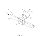
実施の形態3.
実施の形態3にかかる分光測定装置について、図5,及び図6を用いて説明する。図5は、分光測定装置1の光学系を示す模式図である。図5では、左側にYZ平面図が示され、右側にXZ平面図が示されている。図6は、対物レンズ31と試料Sとを模式的に示す斜視図である。図6では駆動ステージ20を省略している。
Embodiment 3.
A spectroscopic measurement device according to a third embodiment will be described with reference to Figs. 5 and 6. Fig. 5 is a schematic diagram showing the optical system of the
実施の形態3では、シート状照明を用いている。シート状照明を用いる点以外については、実施の形態1と同様であるため説明を省略する。例えば、分光器40の入射側には、1つのスリット開口を有するスリット41が設けられている。In the third embodiment, sheet lighting is used. Other than the use of sheet lighting, the third embodiment is similar to the first embodiment, so a description thereof will be omitted. For example, a
照明光L1は、Y方向を光軸方向として試料Sに入射している。照明光L1はX方向に広がったシート状照明光となっている。例えば、照明光学系10において、シリンドリカルレンズを用いることで、シート状照明を形成する。この場合、シリンドリカルレンズはZ方向に照明光L1を集光し、X方向には集光しない。照明光L1は、試料Sにおいて、X方向に広い領域が均一に照明される。つまり、対物レンズ31の視野よりも十分に広い領域が均一な照明光L1で照明される。
The illumination light L1 is incident on the sample S with the optical axis direction being in the Y direction. The illumination light L1 is a sheet-like illumination light that spreads in the X direction. For example, in the illumination
そして、対物レンズ31に対する試料Sの相対位置をX方向に移動させる。例えば、試料Sを載置する駆動ステージをX方向に駆動する。あるいは、対物レンズ31を含む検出光学系30を移動させてもよい。これにより、試料Sにおける光検出器50の検出領域がX方向に変化する。試料Sの二次元領域からのラマン散乱光を検出することができる。ラマン分光画像を高いSN比で撮像することができる。
Then, the relative position of the sample S with respect to the
変形例1
図7は実施の形態3を変形した変形例1にかかる分光測定装置1を示す図である。図7では、左側にYZ平面図が示され、右側にXZ平面図が示されている。図7では、図5の構成に比べてスリット41の方向、及び波長分散方向が異なっている。具体的には、スリット41には、X方向を長手方向とするスリット開口が設けられている。スリット開口はY方向を幅方向としている。
Fig. 7 is a diagram showing a
グレーティング43はX方向と傾いた方向に信号光L2を波長分散する。ここでは、グレーティング43が波長に応じて、Y方向に信号光L2を分散させる。試料Sに対する対物レンズ31の相対位置がY方向に移動する。これにより、XY方向の二次元領域からのラマン散乱光を検出することができる。実施の形態1~3と同様に、高いSN比で、ラマン分光画像を撮像することができる。シート状照明を用いた場合、試料Sを照明する方向、つまり、照明光L1の光軸方向をスリット開口と直交する方向にすることができる。
The grating 43 disperses the signal light L2 in a direction inclined relative to the X direction. Here, the grating 43 disperses the signal light L2 in the Y direction according to the wavelength. The relative position of the
実施の形態4.
実施の形態4にかかる分光測定装置について、図8,及び図9を用いて説明する。図8は、分光測定装置1の光学系を示す模式図である。図8では、左側にYZ平面図が示され、右側にXZ平面図が示されている。図9は、対物レンズ31と試料Sとを模式的に示す斜視図である。なお、図8では、試料Sを省略している。
Embodiment 4.
A spectroscopic measurement device according to a fourth embodiment will be described with reference to Figs. 8 and 9. Fig. 8 is a schematic diagram showing an optical system of the
実施の形態4では、実施の形態3と同様にシート状照明を用いている。したがって、X方向において、対物レンズ31の視野よりも十分に広い領域が照明されている。さらに、実施の形態4では、実施の形態2と同様にマルチスリット41Mを用いている。マルチスリット41Mは、複数のスリット開口を有している。それぞれのスリット開口は、Y方向を長手方向としている。そして、複数のスリット開口がX方向に並んで配置されている。In the fourth embodiment, sheet illumination is used as in the third embodiment. Therefore, in the X direction, an area that is sufficiently wider than the field of view of the
対物レンズ31に対する試料Sの相対位置をX方向に移動する。これにより、XY方向の二次元領域からのラマン散乱光を検出することができる。実施の形態1~3と同様に、高いSN(Signal to Noise)比で、ラマン分光画像を撮像することができる。さらに、複数の領域からの信号光L2を同時に検出することができるため、分光測定の時間を短縮することができる。
The relative position of the sample S with respect to the
変形例2
図10は実施の形態4を変形した変形例2にかかる分光測定装置1を示す図である。図10では、左側にYZ平面図が示され、右側にXZ平面図が示されている。図10では、図8の構成に比べてマルチスリット41Mの方向、及び波長分散方向が異なっている。具体的には、マルチスリット41Mには、X方向を長手方向とするスリット開口が設けられている。スリット開口はY方向を幅方向としている。複数のスリット開口がY方向に並んで配置されている。
Variation 2
Fig. 10 is a diagram showing a
グレーティング43はX方向と傾いた方向に信号光L2を波長分散する。ここでは、グレーティング43が波長に応じて、Y方向に信号光L2を分散させる。試料Sに対する対物レンズ31の相対位置がY方向に移動する。これにより、XY方向の二次元領域からのラマン散乱光を検出することができる。実施の形態1~3と同様に、高いSN比で、ラマン分光画像を撮像することができる。シート状照明を用いた場合、試料Sを照明する方向、つまり、照明光L1の光軸方向をスリット開口と直交する方向にすることができる。
The grating 43 disperses the signal light L2 in a direction inclined relative to the X direction. Here, the grating 43 disperses the signal light L2 in the Y direction according to the wavelength. The relative position of the
上記の実施の形態1~4とその変形例では、対物レンズ31の側方から照明光L1を試料Sに照射させている。つまり、照明光L1と信号光L2とが同軸になっておらず、対物レンズ31を介さず、照明光L1が試料Sに照射する。これにより、高いSN比でラマン散乱光を検出することができる。In the above-mentioned first to fourth embodiments and their modified examples, the illumination light L1 is irradiated onto the sample S from the side of the
(波長分散方向)
上記の実施の形態とその変形例に適用可能な波長分散方向と画素配列方向の一例について、図11を用いて説明する。図11は、マルチスリット41Mと、光検出器50の受光面を示している。
(wavelength dispersion direction)
An example of a wavelength dispersion direction and a pixel array direction applicable to the above embodiment and its modified examples will be described with reference to Fig. 11. Fig. 11 shows a multi-slit 41M and a light receiving surface of a
マルチスリット41Mは、5つのスリット開口A1~A5を備えている。ここでは、スリット開口A1~A5のそれぞれがY方向を長手方向としている。つまり、X方向がスリット開口A1~A5の短手方向(幅方向)となっている。5つのスリット開口A1~A5がX方向に並んでいる。 The multi-slit 41M has five slit openings A1 to A5. Here, the Y direction is the longitudinal direction of each of the slit openings A1 to A5. In other words, the X direction is the short side direction (width direction) of the slit openings A1 to A5. The five slit openings A1 to A5 are lined up in the X direction.
光検出器50の受光面では、X方向、及びY方向に沿って画素が配列されている。そして、波長分散方向をX方向、及びY方向から傾いた斜め方向とする。したがって、スリット開口A1~A5を通過した検出光が検出される検出領域B1~B5が平行四辺形となる。例えば、スリット開口A1を通過した信号光L2が検出領域B1に分散される。同様に、スリット開口A2~A5を通過した信号光L2が検出領域B2~B5にそれぞれ分散される。
On the light receiving surface of the
検出領域B1~B5は、Y方向と平行な2辺を有しており、残りの2辺がX方向から傾いている。X方向から傾いた2辺の方向がグレーティング43による分散方向となる。検出領域B1~B5のそれぞれにおいて、波長分散方向がX方向から傾いている。このようにすることで、測定可能な波長範囲を広げることができ、波長方向におけるデータ数を増やすことができる。なお、検出領域B1~B5は、それぞれ重複しないように設定されている。例えば、検出領域B1の長波長(λn)側と検出領域B2の短波長(λ1)側とがずれている。
Detection regions B1 to B5 have two sides parallel to the Y direction, and the remaining two sides are tilted from the X direction. The direction of the two sides tilted from the X direction is the dispersion direction caused by the
(光学系)
図12は、照明光学系10と検出光学系30の一例を示す図である。図12では、照明領域を走査する光学系の一例が示されている。つまり、光スキャナ108が、照明光L1を偏向させることで、試料Sにおける照明領域が走査される。
(Optical system)
Fig. 12 is a diagram showing an example of the illumination
照明光学系10は、光源101、レンズ102~104、レンズ105、ミラー106、ダイクロイックミラー107、光スキャナ108、レンズ109、ダイクロイックミラー110,ミラー111、レンズ112、レンズ113を備えている。
The illumination
光源101は、例えば、レーザ光源であり、単色の照明光L1を発生する。照明光L1は、レンズ102~105を介して、ミラー106に入射する。なお、レンズ104は、アキシコンレンズやシリンドリカルレンズとなっている。例えば、実施の形態1、2のように、照明光L1をベッセルビームとする場合、レンズ104がアキシコンレンズとなる。あるいは、実施の形態3、4のように、照明光L1をシート状照明とする場合、レンズ104がシリンドリカルレンズとなる。
The
ミラー106は、ダイクロイックミラー107に向けて、照明光L1を反射する。ダイクロイックミラー107は、照明光L1を反射し、ラマン散乱光を透過する波長特性を有している。ダイクロイックミラー107で反射した照明光L1は、光スキャナ108に入射する。光スキャナ108は、例えば、ガルバノミラーであり、照明光L1をX方向に偏向する。これにより、試料Sにおいて照明光L1が走査される。
The
光スキャナ108で反射した照明光L1は、レンズ109を介して、ダイクロイックミラー110に入射する。ダイクロイックミラー110は、照明光L1を反射し、ラマン散乱光を透過する波長特性を有している。ダイクロイックミラー110で反射した照明光L1は、ミラー111に入射する。ミラー111で反射した照明光L1は、レンズ112,レンズ113を介して、試料Sに入射する。レンズ113は、照明用対物レンズである。
The illumination light L1 reflected by the
試料Sにおいて、照明光L1で照明された領域からはラマン散乱光が発生する。ラマン散乱光を検出するための検出光学系30について説明する。検出光学系30は、対物レンズ301、ミラー302,レンズ303、ダイクロイックミラー110、レンズ109と、光スキャナ108、ダイクロイックミラー107、レンズ310、及び分光器40を備えている。ダイクロイックミラー110,レンズ109、光スキャナ108は、検出光学系30と照明光学系10と共通となっている。In the sample S, Raman scattered light is generated from the area illuminated by the illumination light L1. The detection
上記したように、検出光学系30の対物レンズ301の側方から照明光L1が試料Sに入射している。試料Sで発生したラマン散乱光は、対物レンズ301に入射する。対物レンズ301からのラマン散乱光を信号光L2とする。信号光L2はミラー302で反射される。ミラー302からの信号光L2は、レンズ303を介して、ダイクロイックミラー110に入射する。As described above, illumination light L1 is incident on sample S from the side of
ダイクロイックミラー110は、波長に応じて、信号光L2と照明光L1の光路を分岐するビームスプリッタである。ダイクロイックミラー110を透過した信号光L2は、レンズ109を介して、光スキャナ108に入射する。光スキャナ108は、信号光L2をデスキャンする。光スキャナ108で反射した信号光L2は、ダイクロイックミラー107に入射する。The
ダイクロイックミラー107は、波長に応じて、信号光L2と照明光L1の光路を分岐するビームスプリッタである。ダイクロイックミラー107を透過した信号光L2は、レンズ310に入射する。レンズ310は結像レンズであり、試料Sを分光器40のスリット41に結像する。スリット41のスリット開口を通過した信号光L2は、分光器40で波長分散される。分光器40で分散された光は光検出器50で検出される。
The
このような構成であっても、実施の形態と同様に高いSN比でラマン散乱光を検出する。さらに、光スキャナ108を用いて、試料Sにおける照明位置を走査することができる。Even with this configuration, the Raman scattered light is detected with a high signal-to-noise ratio, as in the embodiment. Furthermore, the illumination position on the sample S can be scanned using the
(4π検出)
上記の説明では、+Z方向に放出されたラマン散乱光を検出しているが、+Z方向だけでなく、-Z方向に放出されたラマン散乱光を検出する例について、説明する。+Z方向及び-Z方向に放出するラマン散乱光を検出する構成を4π検出とする。
(4π detection)
In the above description, Raman scattered light emitted in the +Z direction is detected, but an example in which Raman scattered light emitted not only in the +Z direction but also in the -Z direction is detected will be described. A configuration for detecting Raman scattered light emitted in the +Z and -Z directions is referred to as 4π detection.
図13は、試料Sの周辺を模式的に示す側面図である。ここでは、照明光L1がベッセルビームとなっている。試料Sは、例えば、スフェロイド、オルガノイドである。照明光L1で照明された領域からは様々な方向にラマン散乱光が発生する。試料Sから+Z方向に発生したラマン散乱光をラマン散乱光LSuとし、-Z方向に発生したラマン散乱光をラマン散乱光LSdとする。 Figure 13 is a side view showing a schematic view of the periphery of sample S. Here, illumination light L1 is a Bessel beam. Sample S is, for example, a spheroid or an organoid. Raman scattered light is generated in various directions from the area illuminated by illumination light L1. The Raman scattered light generated in the +Z direction from sample S is Raman scattered light LSu, and the Raman scattered light generated in the -Z direction is Raman scattered light LSd.
また、試料Sの+Z側と-Z側にそれぞれ検出用の対物レンズ31が配置されている。試料Sの+Z側にある対物レンズ31を対物レンズ31uとし、-Z側にある対物レンズ31を対物レンズ31dとして図示している。対物レンズ31uと対物レンズ31dとの間に試料Sが配置されている。つまり、対物レンズ31uと対物レンズ31dとは同軸になっている。
Furthermore,
ラマン散乱光LSuは、対物レンズ31uに入射する。対物レンズ31uからのラマン散乱光LSuを信号光L2uとする。信号光L2uは、上記の実施形態と同様に、分光器40で分光されて、検出される。The Raman scattered light LSu is incident on the
ラマン散乱光LSdは、対物レンズ31dに入射する。対物レンズ31dからのラマン散乱光LSdを信号光L2dとする。信号光L2dは、上記の実施形態と同様に、分光器40で分光されて、検出される。例えば、信号光L2u、信号光L2dのそれぞれに対して検出光学系30が設けることができる。このようにすることで、ラマン散乱光の検出光量をほぼ2倍に増やすことができる。The Raman scattered light LSd is incident on the
対物レンズ31u、31dの側方から照明光L1が試料Sに入射している。つまり、照明光L1の光軸が、対物レンズ31uと対物レンズ31dの間の空間を通っている。このようにすることで、高いSN比での検出を行うことができる。ここでは、照明光L1の光軸がY軸と平行になっている。また、高NA、低倍率、広視野の対物レンズを用いることができる。
Illumination light L1 is incident on the sample S from the side of the
図14は、4π検出の別の例を模式的に示す側面図である。図14では、試料Sが基板400の上に配置されている。基板400は、例えば、ステンレス製の金属基板であり、高い光反射率を有している。基板400の主面は、XY平面と平行になっている。基板400の+Z側の面に試料Sが配置されている。試料Sは、例えば細胞シートや基板400上の分子、バクテリアである。対物レンズ31は基板400の+Z側のみに配置されている。
Figure 14 is a side view showing a schematic diagram of another example of 4π detection. In Figure 14, a sample S is placed on a
照明光L1は対物レンズ31の側方から試料Sに照射される。照明光L1の光軸はY方向からわずかに傾いている。例えば、XZ平面視において、照明光L1は-Z方向に進む。照明光L1は、シート状照明とすることができる。
Illumination light L1 is irradiated onto the sample S from the side of the
試料Sからは、ラマン散乱光が様々な方向に放出される。-Z方向に進むラマン散乱光は基板400に入射する。基板400は-Z方向に向かうラマン散乱光を反射する。基板400で反射されたラマン散乱光は、+Z方向に進み、対物レンズ31に入射する。したがって、+Z方向だけでなく、-Z方向に発生したラマン散乱光を対物レンズ31に入射させることができる。対物レンズ31からの検出光は、上記の検出光学系30により、分光器40まで導かれる。このようにすることで、ラマン散乱光の検出光量をほぼ2倍に増やすことができる。また、高NA、低倍率、広視野の対物レンズを用いることができる。
Raman scattered light is emitted in various directions from the sample S. The Raman scattered light traveling in the -Z direction is incident on the
さらに、-Z側に発生したラマン散乱光と、+Z側に放出されたラマン散乱光とで、共通の検出光学系が用いられる。よって、装置構成を簡素化することができる。なお、図14の構成においても、対物レンズ31の側方から照明光L1が試料Sに照射されている。なお、シート状の照明光L1の光軸は、Y方向から傾いていてもよい。例えば、対物レンズ側(+Z側)から照明光L1が試料Sに照射されていてもよい。
Furthermore, a common detection optical system is used for the Raman scattered light generated on the -Z side and the Raman scattered light emitted on the +Z side. This allows the device configuration to be simplified. Note that, even in the configuration of Figure 14, the illumination light L1 is irradiated onto the sample S from the side of the
実施例
以下、本実施形態の実施例について、図15を用いて説明する。図15は、試料を保持する流路チップ500を模式的に示すYZ平面図である。ここでは、試料が流路501~504を流れる流体としている。例えば、流路チップ500は、マイクロチャネルが形成されたマイクロ流路チップである。流路501~504に生体サンプルを流すことができる。例えば、流路501~504には、試料となる細胞やバクテリアが流れている。たとえば、流路に流す試料は、高速液体クロマトグラフィー(HPLC)を経て出射される、成分ごとにわかれたものや、フローサイトメトリーの工程の一部に組み込むという形態でも良い。
Examples An example of this embodiment will be described below with reference to FIG. 15. FIG. 15 is a YZ plan view that shows a
流路チップ500には、X方向に沿って流路501~504が形成されている。流路501~504のそれぞれは、X方向を試料の流路方向とするマイクロチャネルとなっている。流路501~504のYZ断面形状は、矩形となっている。The
X方向に流れる液体の試料に照明光L1が照射される。Y方向に沿って照明光L1が流路501に入射している。つまり、照明光L1の光軸方向と試料の流路方向とが直交している。照明光L1をシート状照明とすることで、流路方向において幅広い領域が照明される。スリット41のスリット開口の長手方向は、Y方向とすることができる。よって、流路方向に幅広い領域を検出領域とすることができる。照明光L1の光軸方向、スリット方向、流路方向は上記の例に限定されるものではない。また、照明光L1を1本又は複数本のベッセルビームとしても良い。
Illumination light L1 is irradiated onto a liquid sample flowing in the X direction. Illumination light L1 is incident on the
流路チップ500において、流路501~504に隣接して反射素子12が設けられている。反射素子12は、流路チップ500に保持されている。レンズ11で集光された照明光L1が反射素子12に入射する。In the
反射素子12は、金属反射面を有するミラーとして機能する。例えば、反射素子12の反射面は、平面となっており、Z軸から45°傾いている。また、流路チップ500の下側にレンズ11が配置されている。なお、反射素子12の反射面は、照明光L1を試料に集光するように凹面となっていてもよい。また、レンズ11の光軸はZ方向と平行になっている。したがって、反射素子12は、レンズ11からの照明光L1を流路501~504に向けて反射する。これにより、流路501~504を流れる試料が照明されて、ラマン散乱光が発生する。The reflecting
以下に示す実施例の基本的な構成は、上記の実施形態と同様であるため、図示を省略すると共に、適宜、説明を省略する。流路501~504がそれぞれ実施例1~4を示している。以下、各実施例について説明する。
The basic configuration of the examples shown below is similar to that of the above embodiment, so illustrations will be omitted and explanations will be omitted as appropriate.
(実施例1)
流路501で示される実施例1について説明する。照明光L1は、流路501の中心に集光されている。照明光L1が流路501に流れる試料に照射されると、ラマン散乱光LSu、LSdが発生する。図13と同様にラマン散乱光LSuは+Z方向の発生したラマン散乱光であり、ラマン散乱光LSdは、-Z方向に発生したラマン散乱光である。そして、流路チップ500の両側にそれぞれ検出光学系30(図15では不図示)を設ける。このようにすることで、様々な方向に放出されたラマン散乱光を検出することができる。
Example 1
A first embodiment shown in a
(実施例2)
流路502で示される実施例2について説明する。照明光L1は、流路502の中心に集光されている。照明光L1が流路502に流れる試料に照射されると、ラマン散乱光LSu、LSdが発生する。流路502の-Z側には、反射鏡322が配置されている。反射鏡322は、流路チップ500の下側に配置されている。反射鏡322は、球面鏡又は楕円面鏡などの凹面鏡となっている。-Z側に反射されたラマン散乱光LSdが反射鏡322に入射すると、+Z方向に反射される。よって、図14と同様に、流路502の+Z側のみに対物レンズ31(図15では不図示)を配置すればよい。ラマン散乱光LSuとラマン散乱光LSdとで検出光学系を共通化できるため、装置構成を簡素化できる。
Example 2
A second embodiment shown by a
(実施例3)
流路503で示される実施例3について説明する。照明光L1が試料全体を照明している。例えば、照明光L1の集光位置が流路503から+Y方向にずれている。よって、流路503の広い領域からラマン散乱光が発生する。このようにすることで、より広い領域からのラマン散乱光を検出することができる。こうすることでZ方向に厚みのある試料からの信号光を効率よく検出することができる。
Example 3
A third embodiment shown by a
また、流路503の-Z側の一面が金属反射面323となっている。したがって、-Z側に放出されたラマン散乱光LSが金属反射面323で反射される。そして、金属反射面323で反射されたラマン散乱光LSは、+Z方向に進む。実施例2と同様に、流路502の+Z側のみに対物レンズ31(図15では不図示)を配置すればよい。したがって、実施例2と同様に、装置構成を簡素化できる。
In addition, one surface on the -Z side of the
(実施例4)
流路504で示される実施例4について説明する。実施例4では、流路504の二面がダイクロイックミラー324として機能している。照明光L1の入射側にはる入射面と、出射側にある出射面がダイクロイックミラー324となっている。ダイクロイックミラー324は、励起光である照明光L1を透過して、ラマン散乱光を反射する。+Y方向、又は-Y方向に放出されたラマン散乱光がダイクロイックミラー324で反射される。
Example 4
A fourth embodiment shown in the
-Z方向成分を有するラマン散乱光は、ダイクロイックミラー324及び金属反射面323で反射される。よって、流路504から+Z方向に取り出される。このようにすることで、+Y方向成分の大きいラマン散乱光を対物レンズ31(図15では不図示)に入射することができる。つまり、Y方向成分がZ方向成分よりも大きいラマン散乱光を検出することができる。よって、実施例2,3よりも光検出器での検出光量を高くすることができる。
Raman scattered light having a -Z direction component is reflected by the
(実施例5)
図16は実施例5の流路505を示す図である。実施例5では、流路505の断面形状が曲面となっている。すなわち、YZ平面視において、流路505が楕円形となっている。流路505の内周面が金属反射面525となっている。流路505の+Z側が取出し部505aとなっている。よって、流路505が積分球として機能する。様々な方向に放出されたラマン散乱光が金属反射面525で反射して、取出し部505aから取り出される。これにより、光検出器での検出光量を高くすることができる。なお、照明光L1が通過する部分は、照明光を透過するように構成する。
Example 5
FIG. 16 is a diagram showing a
(実施例6)
図17は、実施例6に対応する流路506と、実施例7に対応する流路507とを示すYZ平面図である。まず、実施例6について説明する。流路チップ500には、流路506が形成されている。流路506は、X方向に沿って形成されている。照明光L1はシート状照明となっている。流路506の真上には、スリット41が設けられている。スリット41は、流路チップ500の上に載せられている。この構成では、図示しない検出用対物レンズと試料Sとの間にスリット41が配置されていてもよい。
Example 6
17 is a YZ plan view showing a
スリット41は、流路506の方向に沿って形成されている。つまり、スリット41のスリット開口は、X方向を長手方向とし、Y方向を短手方向(スリット幅方向)としている。スリット41のスリット開口部には、フィルタ38が設けられている。フィルタ38は、照明光L1を遮光し、ラマン散乱光を透過する。なお、フィルタ38は、スリット41と流路506との間に設けられているが、スリット41よりも分光器40側に配置されていてもよい。The
このように実施例では、検出用対物レンズよりも試料側にスリット41が設けられている。よって、検出光学系の途中に結像光学系を設ける必要がなくなる。よって、装置構成を簡素化することができる。もちろん、スリット41をマルチスリット41Mとしてもよい。In this embodiment, the
(実施例7)
実施例7にかかる流路507では、実施例6の構成に対して集光素子527が追加されている。具体的には、流路507の上に集光素子527が設けられている。集光素子527は、ラマン散乱光を集光するレンズとして機能する。集光素子527で集光されたラマン散乱光がスリット41に入射する。例えば、集光素子527は、流路チップ500内に設けられている。あるいは、流路507の+Z側の部分を曲面とすることで、流路チップ500内に、集光素子527を実装することができる。集光素子527は、X方向を長手方向とするシリンドリカルレンズであってもよい。
(Example 7)
In the
このようにすることで、検出NAを大きくすることができる。よって、空間分解能を高くすることができる。さらに、分光器40の分光光学系の入射NAを小さくすることができる。By doing so, the detection NA can be increased, and the spatial resolution can be increased. Furthermore, the incident NA of the spectroscopic optical system of the
(実施例8)
図18は、実施例8を示すYZ平面図である。実施例8では、流路508の近傍にフィルタ16が設けられている。フィルタ16は、例えば、照明光L1となるレーザ光のレーザ波長を透過するレーザラインフィルタやバンドパスフィルタである。フィルタ16は、反射素子12と流路508との間に配置されている。照明用対物レンズであるレンズ11と試料との間の光路中にフィルタ16が配置されている。このように、レンズ11と試料との間にフィルタ16を設けることで、レーザ波長以外の光が試料に入射することを防ぐことができる。レーザ波長の光のみでラマン散乱光が発生する。よって、信号光のノイズを低減することができ、適切にラマン分光測定を行うことができる。
(Example 8)
FIG. 18 is a YZ plane view showing the eighth embodiment. In the eighth embodiment, a
(実施例9)
図19は、実施例9を示すYZ平面図である。実施例9においても、試料Sとレンズ11との間にフィルタ16が配置されている。レンズ11は、上記のように試料Sに照明光L1を集光する照明用対物レンズである。レンズ11の光軸は、Y方向と平行になっている。レンズ11によって集光された照明光L1がフィルタ16を介して、試料Sに入射する。例えば、照明光L1となるレーザ光のレーザ波長を透過するレーザラインフィルタやバンドパスフィルタである。フィルタ16は厚さ300μm程度となっている。このような構成によっても、レーザ波長以外の光が試料に入射することを防ぐことができる。レーザ波長の光のみでラマン散乱光が発生する。よって、信号光のノイズを低減することができ、適切にラマン分光測定を行うことができる。
Example 9
FIG. 19 is a YZ plane view showing Example 9. In Example 9, a
(偏光状態)
次に、照明光L1の偏向状態の一例について、図20を用いて説明する。図20は、試料周辺の構成を示すYZ平面図であり。照明光L1の偏光状態を模式的に示している。ここでは、試料に集光される照明光L1が、照明光L1の光軸(Y方向)と平行な偏光状態となっている。照明光L1はシート照明となっている。また、スリット41のスリット開口は、Y方向と平行になっている。
(Polarization state)
Next, an example of the deflection state of the illumination light L1 will be described with reference to Fig. 20. Fig. 20 is a YZ plane view showing the configuration around the sample. The polarization state of the illumination light L1 is shown diagrammatically. Here, the illumination light L1 focused on the sample is in a polarization state parallel to the optical axis (Y direction) of the illumination light L1. The illumination light L1 is sheet illumination. Also, the slit opening of the
レンズ11と、試料Sとの間には、偏光制御素子17が配置されている。偏光制御素子17は、分割波長板である。偏光制御素子17は、2分割であることが望ましい。さらに、照明光L1は、レンズ11で集光されている。よって、レンズ11の焦点位置では、照明光L1は、その光軸方向に大きな電場成分を作り出すことができる。つまり、検出位置において、照明光L1の偏光方向が光軸方向と平行になる。なお、偏光制御素子17は、レンズ11よりも光源側に配置されていてもよい。
A
このようにすることで、スリット41に入射する信号光L2はスリット開口と平行な偏光成分が大きくなる。グレーティング43に入射する信号光L2において、P偏光成分が大きくなる。例えば、グレーティング43に入射する信号光L2がP偏光の時、グレーティング43の溝方向と電場ベクトルの振動方向が平行になり、S偏光の時、溝方向と電場ベクトルの振動方向が直交する。よって、グレーティング43の回折効率を高くすることができる。グレーティングの特性や、観察対象となる波長領域によって偏光特性が異なってくるため、条件に応じて偏光を制御する。
By doing this, the signal light L2 incident on the
上記の実施の形態、変形例、実施例のそれぞれは適宜組み合わせて用いることができる。例えば、シート状照明、ベッセルビーム、マルチビームのいずれについても、光路中にフィルタ16を用いても良い。シート状照明、ベッセルビーム、マルチビームのいずれについても、4π検出を行ってもよい。実施の形態、変形例、実施例の2つ以上を適宜組み合わせても良い。
The above-mentioned embodiments, modifications, and examples may be used in appropriate combination. For example, a
また、ベッセルビーム、シート照明に限らず、ラティス照明を用いてもよい。ラティス照明を用いることで、試料Sを格子状の照明パターンで照明することができる。また、信号光L2の光路中に照明光L1の波長の光を遮光し、ラマン散乱光を透過するエッジフィルタを配置してもよい。 In addition, lattice illumination may be used instead of Bessel beam and sheet illumination. By using lattice illumination, the sample S can be illuminated with a lattice-shaped illumination pattern. Also, an edge filter that blocks light of the wavelength of the illumination light L1 and transmits Raman scattered light may be placed in the optical path of the signal light L2.
さらに流路内を流れている試料を分光測定する場合、例えば、以下の3つの露光方法を用いることができる。
1)流路内の試料を止めて計測し、計測終了後に流して次の試料を測定する。
2)流路に試料を流しながら測定する。このとき、CCDカメラのチャージシフト速度と流路内の試料の流速を同じにして、同一試料からの信号光を単一の画素に積算する。
3)流路に試料を流しながら測定する。このとき、短い露光時間で複数回測定した後、データ処理により、単一試料の信号を積算する。測定時間における試料の場所は、レイリー散乱などの顕微観察で計測しておく。この計測結果を基に、同一試料からのラマンデータをCCD上で抽出して積算する。光検出器50の異なる画素で同一試料からの信号光が検出される。つまり、流路を流れる同一試料からの信号光が光検出器50で複数回検出される。光検出器50の異なる画素の検出信号を積算して、同一試料からのラマン散乱光とする。
Furthermore, when spectroscopic measurement is performed on a sample flowing inside a flow channel, for example, the following three exposure methods can be used.
1) The sample in the flow path is stopped and measured, and after the measurement is completed, the next sample is allowed to flow and measured.
2) Measurement is performed while the sample is flowing through the flow channel. At this time, the charge shift speed of the CCD camera and the flow speed of the sample in the flow channel are made the same, and signal light from the same sample is integrated into a single pixel.
3) Measurement is performed while the sample is flowing through the flow path. At this time, measurements are performed multiple times with short exposure times, and then the signals from a single sample are integrated by data processing. The location of the sample at the measurement time is measured by microscopic observation such as Rayleigh scattering. Based on this measurement result, Raman data from the same sample is extracted and integrated on a CCD. Signal light from the same sample is detected by different pixels of the
流体内の細胞あるいはバクテリアを観察するときは読み出しノイズを減らすことが有効である。細胞(バクテリア):カメラの画素=1:1に近い総合倍率にすることが好ましい。試料の細胞が光検出器50の1画素に対応している。例えば、装置全体の倍率が1倍の時は、細胞直径、20μmと仮定すると、細胞は(1×n)画素に収まるようになる。nは2以上の整数であり、ラマン散乱光の分散方向の画素数に相当する。CCDカメラとして、例えば、テレダイン社PIXIS400B、1画素20μm四方を用いることができる。細胞の大きさや目的によって倍率は変更できる。他にも、例えば装置全体の倍率5倍程度で観察した場合には、細胞直径、20μmと仮定すると、細胞は(5×n)画素に収まるようになる。総合倍率を下げることでSN比の向上を図ることができる。光検出器50の1画素が試料の細胞に対応している。例えば、細胞が1画素のサイズと同等になって検出されるように、対物レンズ31などの倍率を決定すればよい。
When observing cells or bacteria in a fluid, it is effective to reduce the readout noise. It is preferable to set the total magnification close to 1:1 (cell (bacteria): camera pixel). A sample cell corresponds to one pixel of the
ここで、光検出器50は分光器40で分散された信号光を検出している。したがって、光検出器50の受光面では、細胞からの信号光が分散方向に拡がる。光検出器50の1画素が試料の細胞に対応するような倍率が設定されていたとしても、分散方向では、細胞からの信号光が複数の画素で検出される。光検出器50の(1×n)個の画素で細胞からの信号光が検出される。換言すると、分散方向と直交する方向において、細胞からの信号光は光検出器50の1つの画素で検出される。波長分散素子の波長分散方向と直交する方向において試料の細胞が光検出器50の1画素に対応するような倍率で信号光L2が検出されていることが好ましい。波長分散方向と直交する方向において、細胞が5画素以下に収まるような倍率で測定することが好ましく、1画素以下に収まるような倍率で測定することがさらに好ましい。Here, the
また、照明光L1が、検出用の対物レンズ31の光軸方向に走査されていてもよい。例えば、流路を流れる試料の場合、画像を取得するのではなく、試料全体のスペクトルを取得することも可能である。この場合、高さ方向(検出用の対物レンズ31の光軸方向)にも一様に照明したいため、側方照明をその方向に高速走査しながら、細胞全体を照明する。例えば、図1~図10などの構成において、Z方向に照明光L1を走査する。
The illumination light L1 may also be scanned in the optical axis direction of the
上記の説明では、試料又は照明光を走査しながら分光測定を行ったが、試料又は照明光を走査しなくてもよい。例えば、試料を流路に流しながら測定を行ってもよい。つまり、試料又は照明光を走査する手段の代わりに、試料を流路に流す手段があってもよい。In the above explanation, spectroscopic measurements were performed while scanning the sample or illumination light, but the sample or illumination light does not have to be scanned. For example, measurements may be performed while the sample is flowing through a flow path. In other words, instead of a means for scanning the sample or illumination light, there may be a means for flowing the sample through a flow path.
また、図12では、レンズ113の光軸が水平方向と平行であり、対物レンズ301の光軸が鉛直方向と平行であるが、光軸は水平方向、及び鉛直方向から傾いていても良い。照明光及び検出光の光軸は水平方向、及び鉛直方向が傾いている構成の一例を図21に示す。
In addition, in Fig. 12, the optical axis of
図21では、ディッシュ600内に水601が貯留されている。さらに、ディッシュ600内には、試料Sを保持する試料基板603が配置されている。試料基板603の上に試料Sが載置されている。In FIG. 21,
ディッシュ600の上側に対物レンズ31とレンズ11とが配置されている。対物レンズ31とレンズ11とが試料Sの斜め上方に配置されている。試料Sの斜め上方から照明光L1が試料Sに照射されている。レンズ11からの照明光L1は水中を伝播して、試料Sに入射する。また、試料Sで発生して斜め上方に進むラマン散乱光が対物レンズ31に入射する。試料Sからのラマン散乱光は、水中を伝播して、対物レンズ31に入射する。
照明光及び検出光の光軸は水平方向、及び鉛直方向が傾いている構成の別の一例を図22に示す。図22では、ディッシュ600内に水601が貯留されている。さらに、ディッシュ600内に試料Sが配置されている。ディッシュ600はガラスなどの透明材料で形成されている。Another example of a configuration in which the optical axes of the illumination light and the detection light are tilted horizontally and vertically is shown in Figure 22. In Figure 22,
対物レンズ31とレンズ11とがディッシュ600の下方に配置されている。つまり、試料Sの斜め下方から照明光L1が試料Sに照射されている。レンズ11からの照明光L1のディッシュ600の底部を透過して試料Sに入射する。また、試料Sで発生して斜め下方に進むラマン散乱光が対物レンズ31に入射する。試料Sからのラマン散乱光は、ディッシュ600の底部を透過して対物レンズ31に入射する。
The
なお、上記の実施の形態では、主として、信号光がラマン散乱光であるとして説明したが、信号光は、ラマン散乱光以外の光であってもよい。したがって、本実施の形態にかかる分光測定装置は、ラマン分光以外の分光測定装置であってもよい。例えば、励起光によって励起される蛍光を検出する分光測定装置や、赤外吸収スペクトルや近赤外吸収スペクトルを測定する分光測定装置であってもよい。これらの分光測定装置でも、高いSN比で、スペクトルの測定を行うことができる。特に、高速計測や繰り返し計測を求められる分光測定装置に好適である。分光測定装置の用途は、イメージングに限られるものではない。試料が溶液などの一様な試料の場合は広い面積を同時に計測できるので信号量が増し、測定時間を短くできる。この場合計測されたスペクトルは積算される。In the above embodiment, the signal light is mainly described as Raman scattered light, but the signal light may be light other than Raman scattered light. Therefore, the spectroscopic measurement device according to this embodiment may be a spectroscopic measurement device other than Raman spectroscopy. For example, it may be a spectroscopic measurement device that detects fluorescence excited by excitation light, or a spectroscopic measurement device that measures infrared absorption spectrum or near-infrared absorption spectrum. These spectroscopic measurement devices can also measure spectra with a high S/N ratio. In particular, it is suitable for spectroscopic measurement devices that require high-speed measurement or repeated measurement. The use of the spectroscopic measurement device is not limited to imaging. When the sample is a uniform sample such as a solution, a wide area can be measured simultaneously, so the signal amount increases and the measurement time can be shortened. In this case, the measured spectrum is integrated.
分光測定装置1は自発ラマン散乱光を分光測定することができる。また、分光測定装置1は誘導ラマン散乱光を分光測定してもよい。誘導ラマン散乱光を測定する場合、ポンプ光とストークス光を試料に照射してもよい。つまり、異なる波長の2つのレーザ光源が用いられる。この場合、ポンプ光とストークス光が側方から試料に照射されるように配置すればよい。The
次に、図23~図25を用いて、スリットの方向に対する流路の方向について説明する。図23~図25は、流路チップ500に設けられた流路501を模式的に示す図である。図23は、スリットの長手方向が流路501の方向と平行の場合の構成を模式的に示す図である。図24は、スリットの長手方向が流路501の方向から傾いている場合の構成を模式的に示す図である。図25は、流路501が蛇行している構成を模式的に示す図である。
Next, the direction of the flow channel relative to the direction of the slit will be explained using Figures 23 to 25. Figures 23 to 25 are diagrams that show a
図23~図25はスリットのスリット開口A1を流路チップ500上に投影して示している。図23~図25において、スリット開口A1の長手方向がX方向と平行になっている。つまり、スリット開口A1の幅方向がY方向となっている。スリット開口A1に対応する領域が流路501の検出領域となる。また、照明方向がY方向と平行になっている。紙面と直交するZ方向が対物レンズの光軸と平行になる。
Figures 23 to 25 show the slit opening A1 of the slit projected onto the
図23では、測定対象の試料710、711が流路501内を流れている。ここで、試料710、711は、細胞などの生体試料とすることができる。流路501には、試料710、711を流すための流体が供給されている。図23では、流路501はX方向に沿って設けられている。よって、試料710、711がX方向に流れていく。
In Fig. 23,
図23では、スリット開口A1の長手方向と、流路501の方向が平行となっている。図24では、スリット開口A1の長手方向が、流路501の方向から傾いている。つまり、流路501の方向が、X方向及びY方向から傾いている。In Fig. 23, the longitudinal direction of the slit opening A1 is parallel to the direction of the
図24では、試料710がスリット開口A1に対応する検出領域を横切るように流路501を流れていく。よって、図24の構成では、試料710のより広い範囲からの信号光を検出することができるようになる。例えば、スリット開口A1の幅に対応するサイズよりも流路501の幅が広くなっていると仮定する。図23に示すように、Y方向において流路501の中心からずれて流路501を流れている試料711があるとする。この場合、試料711の一部からの信号光のみしか検出することができない。In FIG. 24,
図24の構成では、いずれの試料710も、スリット開口A1に対応する検出領域を横切ることができる。よって、試料710の全体がスリット開口A1に対応する検出領域を通過する。試料710がスリット開口A1を横切る間、光検出器50が信号光を検出することで、試料710のより広い範囲からの信号光を測定することができる。In the configuration of FIG. 24, any
図25では、流路501が蛇行するように曲げられている。流路501を流れる試料710がY方向に往復する。つまり、試料710は、流路501に沿って、+Y方向及び-Y方向に交互に流れていく。試料710がスリット開口A1に対応する検出領域を繰り返し横切るように、流路501を流れていく。このようにすることで、試料710の分光測定を繰り返し行うことができる。
In Figure 25, the
さらに、図25に示すように、流路チップ500の少なくとも一部に冷却領域702を設けるようにしてもよい。冷却領域702では流路チップ500が冷却されている。たとえば、冷却領域702では冷媒など冷却手段が流路チップ500に接触している。このようにすることで、試料710である細胞を冷却しながらの分光測定が可能となる。よって、試料710への光ダメージを低減することができる。
Furthermore, as shown in FIG. 25, a
さらに、流路501の途中に、支流703が設けられていてもよい。支流703から溶液などを供給することで、試料710の流速を変えることができる。つまり、流速を変えて測定を行うことができる。Furthermore, a
さらに、試料710と反応する溶液や薬剤を支流703から供給してもよい。このようにすることで、反応によるスペクトルの変化を測定することが可能となる。つまり、反応前、反応途中、反応後のスペクトルを測定することができる。
In addition, a solution or chemical that reacts with the
次に、同一試料からの信号光を画素に積算する方法について。図26~図28を用いて説明する。図26~図28は流路501を流れる試料710と光検出器50の画素の動作を示す模式図である。試料710は流路501を流れる細胞などである。試料710は、溶液などの流体とともに流路501を流れていく。図26~図28に示すようにスリット方向と分光方向は直交する方向になっている。
Next, a method of integrating signal light from the same sample in a pixel will be described with reference to Figs. 26 to 28. Figs. 26 to 28 are schematic diagrams showing a
また、図26~図28では、光検出器50の4列分の画素列が模式的に示されている。1列目の画素を画素列151としている。同様に、2列目、3列目、4列目の画素列を画素列152~154としている。ここでは、CCDカメラのチャージシフト速度と流路内の試料の流速を同じにしている。26 to 28 also show four pixel rows of the
1つの画素列でラマンスペクトルが測定される。つまり、画素列151に含まれる画素の配列方向が分光器40の分光方向と平行になっている。分光方向と直交する直交方向が、流路の方向に対応している。したがって、流路501を流れる試料710からの信号光は、画素列151,画素列152、画素列153、画素列154の順番で検出される。
The Raman spectrum is measured in one pixel row. In other words, the arrangement direction of the pixels included in
ここで、試料710が流路501を流れる速度と、画素列間の信号電荷の転送速度とが一致するように、流速を調整する。例えば、図26では、試料710が画素列151に対応する位置に存在している。画素列151の画素では、受光量に応じた信号電荷が発生する。そして、CCDが1列目の画素列151の画素が発生した信号電荷を読みだす。図26では、試料710からの信号光が画素列151の各画素で検出される。Here, the flow rate is adjusted so that the speed at which the
試料710が図27,図28に示すように流路501を流れていく。図27では、試料710が画素列151と画素列152との間に対応する位置に移動している。画素列151の画素で読み出された信号電荷が、画素列152に転送される。27 and 28, the
そして、図28に示すように、試料710が画素列152に対応する位置に移動する。すると、画素列152の各画素が受光量に応じた信号電荷を発生する。図28では、試料710からの信号光が画素列152の各画素で検出される。CCDが2列目の画素列152の画素が発生した信号電荷を読みだす。したがって、1列目の画素列の画素で発生した信号電荷と、2列目の画素列152の画素で発生した信号電荷が積算される。
Then, as shown in Figure 28, the
このようにすることで、複数の画素で発生した信号電荷を積算することができる。つまり、4列分の画素列151~154の信号電荷が波長毎に積算される。分光方向と直交する方向における画素アドレスが異なったとしても、同じ試料710からの信号光が検出される。よって、SN比を向上することができる。もちろん、画素の積算数は、4つに限定されるものではない。
In this way, the signal charges generated in multiple pixels can be accumulated. In other words, the signal charges of four
このように、流路501内を流れる試料710を分光測定する場合、試料の流速を信号電荷の転送速度と対応する速度に調整する。そして、光検出器50において、複数の画素の信号電荷を積算していく。同じ試料710からの信号光L2が複数の画素列で蓄積されて、検出される。これにより、より高いSN比での測定が可能となる。In this way, when performing spectroscopic measurement of the
以上、本発明者によってなされた発明を実施の形態に基づき具体的に説明したが、本発明は上記実施の形態に限られたものではなく、その要旨を逸脱しない範囲で種々変更可能であることは言うまでもない。The invention made by the inventor has been specifically described above based on an embodiment, but it goes without saying that the present invention is not limited to the above embodiment and can be modified in various ways without departing from the gist of the invention.
この出願は、2021年2月4日に出願された日本出願特願2021-16751を基礎とする優先権を主張し、その開示の全てをここに取り込む。 This application claims priority based on Japanese Patent Application No. 2021-16751, filed on February 4, 2021, the disclosure of which is incorporated herein in its entirety.
1 分光測定装置
10 照明光学系
11 レンズ
16 フィルタ
17 偏光制御素子
30 検出光学系
31 対物レンズ
32 レンズ
40 分光器
41 スリット
42 レンズ
43 グレーティング
44 レンズ
50 光検出器
51 処理部
101 光源
102~105 レンズ
106 ミラー
107 ダイクロイックミラー
108 光スキャナ
109 レンズ
500 流路チップ
501~508 流路
702 冷却領域
703 支流
710 試料
L1 照明光
L2 信号光
REFERENCE SIGNS
Claims (17)
前記信号光が通過するスリット開口を有するスリットと、
前記スリット開口を通過した信号光を波長に応じて分散する波長分散素子と、
前記信号光に基づいて前記試料の所定の範囲のラマン散乱光を積算又はイメージングするために、前記波長分散素子で波長分散された信号光を検出する二次元光検出器と、
前記検出用対物レンズの検出光軸方向と直交する方向を照明光軸方向として照明光を前記試料に集光し、前記検出用対物レンズの側方から照明光を前記試料に入射させる照明光学系と、
前記スリットが、前記検出用対物レンズの焦点面と共役な位置に配置され、
前記照明光学系が、前記照明光をシート照明として試料に集光し、
前記照明光学系は、前記検出用対物レンズの検出光軸方向に前記シート照明を集光し、
前記検出光軸方向と直交する直交平面内において、前記スリット開口の長手方向と直交する直交方向に前記検出用対物レンズの視野よりも広がったシート照明となっており、
前記スリット開口の長手方向において、異なる位置からの信号光を前記二次元光検出器の異なる画素で検出して、ラマンスペクトルを測定し、
前記検出光軸方向又は前記直交平面内の前記直交方向に、前記検出用対物レンズに対する前記試料の相対位置を移動させる
分光測定装置。 a detection objective lens onto which signal light , which is Raman scattered light from a sample, is incident;
a slit having a slit opening through which the signal light passes;
a wavelength dispersion element that disperses the signal light passing through the slit opening according to the wavelength;
a two-dimensional photodetector that detects the signal light that has been wavelength-dispersed by the wavelength dispersion element in order to integrate or image the Raman scattered light in a predetermined range of the sample based on the signal light ;
an illumination optical system that focuses illumination light onto the sample with an illumination optical axis direction perpendicular to a detection optical axis direction of the detection objective lens and causes the illumination light to be incident on the sample from a side of the detection objective lens;
the slit is disposed at a position conjugate with a focal plane of the detection objective lens,
the illumination optical system focuses the illumination light onto a sample as sheet illumination;
the illumination optical system condenses the sheet illumination in a detection optical axis direction of the detection objective lens,
In an orthogonal plane perpendicular to the detection optical axis direction, the sheet illumination is wider than the field of view of the detection objective lens in an orthogonal direction perpendicular to the longitudinal direction of the slit opening,
detecting signal light from different positions in a longitudinal direction of the slit opening with different pixels of the two-dimensional photodetector to measure a Raman spectrum;
A relative position of the sample with respect to the detection objective lens is moved in the detection optical axis direction or in the orthogonal direction within the orthogonal plane.
Spectroscopic measurement equipment.
前記照明用対物レンズと前記試料との間に配置され、前記照明光を透過し、レーザ波長以外の波長の光を遮光するフィルタをさらに備えた請求項1~5のいずれか1項に記載の分光測定装置。6. The spectroscopic measurement device according to claim 1, further comprising a filter disposed between the illumination objective lens and the sample, the filter transmitting the illumination light and blocking light of wavelengths other than the laser wavelength.
前記信号光が通過するスリット開口を有するスリットと、
前記スリット開口を通過した信号光を波長に応じて分散する波長分散素子と、
前記信号光に基づいて前記試料の所定の範囲のラマン散乱光を積算又はイメージングするために、前記波長分散素子で波長分散された信号光を検出する二次元光検出器と、
前記検出用対物レンズの側方から照明光であるレーザ光を前記試料に入射させる照明光学系と、
前記照明光を前記試料に集光する照明用対物レンズと、
前記照明用対物レンズと前記試料との間に配置され、前記照明光を透過し、レーザ波長以外の波長の光を遮光するフィルタとを備え、
前記スリットが、前記検出用対物レンズと共役な位置に配置され、
前記照明光学系が、前記照明光をシート照明として試料に集光し、
検出用対物レンズの検出光軸方向と直交する直交平面内において、前記スリット開口の長手方向と直交する直交方向に前記検出用対物レンズの視野よりも広がったシート照明となっており、
前記スリット開口の長手方向において、異なる位置からの信号光を前記二次元光検出器の異なる画素で検出して、ラマンスペクトルを測定し、
前記検出光軸方向又は前記直交平面内の前記直交方向に、前記検出用対物レンズに対する前記試料の相対位置を移動させる、
分光測定装置。 a detection objective lens onto which signal light , which is Raman scattered light from a sample, is incident;
a slit having a slit opening through which the signal light passes;
a wavelength dispersion element that disperses the signal light passing through the slit opening according to the wavelength;
a two-dimensional photodetector that detects the signal light that has been wavelength-dispersed by the wavelength dispersion element in order to integrate or image the Raman scattered light in a predetermined range of the sample based on the signal light ;
an illumination optical system that causes laser light, which is illumination light, to be incident on the sample from a side of the detection objective lens;
an illumination objective lens that focuses the illumination light onto the sample;
a filter disposed between the illumination objective lens and the sample, the filter transmitting the illumination light and blocking light of wavelengths other than the laser wavelength ;
the slit is disposed at a position conjugate with the detection objective lens,
the illumination optical system focuses the illumination light onto a sample as sheet illumination;
In an orthogonal plane perpendicular to a detection optical axis direction of the detection objective lens, the sheet illumination is wider than the field of view of the detection objective lens in an orthogonal direction perpendicular to a longitudinal direction of the slit opening,
detecting signal light from different positions in a longitudinal direction of the slit opening with different pixels of the two-dimensional photodetector to measure a Raman spectrum;
moving a relative position of the sample with respect to the detection objective lens in the detection optical axis direction or in the orthogonal direction within the orthogonal plane;
Spectroscopic measurement equipment.
前記試料において、前記照明光軸方向と平行な方向の偏光状態にする偏光制御素子とを、さらに備え、
前記スリット開口が前記照明光軸方向に沿って形成されている請求項1~7のいずれか1項に記載の分光測定装置。 an illumination objective lens that focuses the illumination light onto the sample;
a polarization control element for causing the sample to be polarized in a direction parallel to the illumination optical axis direction ,
8. The spectroscopic measurement device according to claim 1, wherein the slit opening is formed along the illumination optical axis direction .
流路を流れている同一試料からの信号光が前記二次元光検出器の異なる画素で検出されており、
同一試料からの信号光を検出した前記異なる画素からの検出信号を積算する請求項1~10のいずれか1項に記載の分光測定装置。 a flow rate of the sample flowing through the flow channel and a transfer rate of a signal charge in the two-dimensional photodetector are equal to each other;
signal light from the same sample flowing through the flow channel is detected by different pixels of the two-dimensional photodetector;
11. The spectroscopic measurement device according to claim 1, wherein detection signals from the different pixels that detect signal light from the same sample are integrated.
それぞれの前記検出用対物レンズからの信号光が波長分散素子で波長分散されて、2次元光検出器で検出される請求項1~13のいずれか1項に記載の分光測定装置。14. The spectroscopic measurement device according to claim 1, wherein the signal light from each of the detection objective lenses is wavelength-dispersed by a wavelength dispersion element and detected by a two-dimensional photodetector.
前記試料から前記検出用対物レンズと反対側に発生した信号光が前記基板で反射して、前記検出用対物レンズに入射する請求項1~14のいずれか1項に記載の分光測定装置。15. The spectroscopic measurement device according to claim 1, wherein signal light generated from the sample on a side opposite to the detection objective lens is reflected by the substrate and enters the detection objective lens.
前記検出用対物レンズに試料からのラマン散乱光である信号光が入射するステップと、
前記信号光がスリットのスリット開口を通過するステップと、
前記スリット開口を通過した信号光を波長分散素子により波長分散するステップと、
前記信号光に基づいて前記試料の所定の範囲のラマン散乱光を積算又はイメージングするために、二次元光検出器を用いて前記波長分散素子で波長分散された信号光を検出するステップと、を備え、
前記照明光学系は、前記検出用対物レンズの検出光軸方向と直交する方向を照明光軸方向として照明光を試料に集光し、
前記スリットが、前記検出用対物レンズの焦点面と共役な位置に配置され、
前記照明光学系が、前記照明光をシート照明として試料に集光し、
前記照明光学系は、前記検出用対物レンズの検出光軸方向に前記シート照明を集光し、
前記検出光軸方向と直交する直交平面内において、前記スリット開口の長手方向と直交する直交方向に前記検出用対物レンズの視野よりも広がったシート照明となっており、
前記スリット開口の長手方向において、異なる位置からの信号光を前記二次元光検出器の異なる画素で検出して、ラマンスペクトルを測定し、
前記検出光軸方向又は前記直交平面内の前記直交方向に、前記検出用対物レンズに対する前記試料の相対位置を移動させる、
分光測定方法。 Illuminating the sample from a side of the detection objective using an illumination optical system;
A step in which signal light , which is Raman scattered light from a sample, is incident on the detection objective lens;
the signal light passing through a slit opening of a slit ;
a step of dispersing the signal light passing through the slit opening by a wavelength dispersion element;
detecting the signal light wavelength-dispersed by the wavelength dispersive element using a two-dimensional photodetector in order to integrate or image the Raman scattered light in a predetermined range of the sample based on the signal light ;
the illumination optical system focuses illumination light onto a sample, with the illumination optical axis being perpendicular to the detection optical axis direction of the detection objective lens;
the slit is disposed at a position conjugate with a focal plane of the detection objective lens,
the illumination optical system focuses the illumination light onto a sample as sheet illumination;
the illumination optical system condenses the sheet illumination in a detection optical axis direction of the detection objective lens,
In an orthogonal plane perpendicular to the detection optical axis direction, the sheet illumination is wider than the field of view of the detection objective lens in an orthogonal direction perpendicular to the longitudinal direction of the slit opening,
detecting signal light from different positions in a longitudinal direction of the slit opening with different pixels of the two-dimensional photodetector to measure a Raman spectrum;
moving a relative position of the sample with respect to the detection objective lens in the detection optical axis direction or in the orthogonal direction within the orthogonal plane;
Spectroscopic methods.
Applications Claiming Priority (3)
| Application Number | Priority Date | Filing Date | Title |
|---|---|---|---|
| JP2021016751 | 2021-02-04 | ||
| JP2021016751 | 2021-02-04 | ||
| PCT/JP2021/046916 WO2022168467A1 (en) | 2021-02-04 | 2021-12-20 | Spectrometry device and spectrometry method |
Publications (3)
| Publication Number | Publication Date |
|---|---|
| JPWO2022168467A1 JPWO2022168467A1 (en) | 2022-08-11 |
| JPWO2022168467A5 JPWO2022168467A5 (en) | 2023-11-02 |
| JP7527041B2 true JP7527041B2 (en) | 2024-08-02 |
Family
ID=82742172
Family Applications (1)
| Application Number | Title | Priority Date | Filing Date |
|---|---|---|---|
| JP2022579380A Active JP7527041B2 (en) | 2021-02-04 | 2021-12-20 | Spectroscopic measurement device and spectroscopic measurement method |
Country Status (4)
| Country | Link |
|---|---|
| US (1) | US20240110830A1 (en) |
| EP (1) | EP4290217A4 (en) |
| JP (1) | JP7527041B2 (en) |
| WO (1) | WO2022168467A1 (en) |
Citations (3)
| Publication number | Priority date | Publication date | Assignee | Title |
|---|---|---|---|---|
| JP2006113021A (en) | 2004-10-18 | 2006-04-27 | Univ Waseda | Raman spectroscopic device and spectroscopic device |
| JP2018128325A (en) | 2017-02-07 | 2018-08-16 | ナノフォトン株式会社 | Spectroscopic microscope, and spectroscopic observation method |
| JP2021500558A (en) | 2017-10-23 | 2021-01-07 | ザ ユナイテッド ステイツ オブ アメリカ, アズ リプレゼンテッド バイ ザ セクレタリー, デパートメント オブ ヘルス アンド ヒューマン サービシーズ | Optical Configuration Method for Spectral Scattered Flow Cytometry |
Family Cites Families (5)
| Publication number | Priority date | Publication date | Assignee | Title |
|---|---|---|---|---|
| DE69636967T2 (en) * | 1995-09-20 | 2007-12-20 | Arkray, Inc. | Method for analysis by means of light scattering |
| JP2009063462A (en) * | 2007-09-07 | 2009-03-26 | Sony Corp | Optical measuring instrument and particulate analyzer |
| JP5337676B2 (en) * | 2009-06-25 | 2013-11-06 | 株式会社日立ハイテクノロジーズ | Fluorescence analyzer and fluorescence detector |
| JP2019045625A (en) * | 2017-08-31 | 2019-03-22 | 国立大学法人北陸先端科学技術大学院大学 | Shg microscope and method for observing shg light |
| JP2021016751A (en) | 2019-07-17 | 2021-02-15 | 有限会社トライ金型 | Small container with cooling function |
-
2021
- 2021-12-20 US US18/275,245 patent/US20240110830A1/en active Pending
- 2021-12-20 EP EP21924852.3A patent/EP4290217A4/en active Pending
- 2021-12-20 WO PCT/JP2021/046916 patent/WO2022168467A1/en active Application Filing
- 2021-12-20 JP JP2022579380A patent/JP7527041B2/en active Active
Patent Citations (3)
| Publication number | Priority date | Publication date | Assignee | Title |
|---|---|---|---|---|
| JP2006113021A (en) | 2004-10-18 | 2006-04-27 | Univ Waseda | Raman spectroscopic device and spectroscopic device |
| JP2018128325A (en) | 2017-02-07 | 2018-08-16 | ナノフォトン株式会社 | Spectroscopic microscope, and spectroscopic observation method |
| JP2021500558A (en) | 2017-10-23 | 2021-01-07 | ザ ユナイテッド ステイツ オブ アメリカ, アズ リプレゼンテッド バイ ザ セクレタリー, デパートメント オブ ヘルス アンド ヒューマン サービシーズ | Optical Configuration Method for Spectral Scattered Flow Cytometry |
Also Published As
| Publication number | Publication date |
|---|---|
| WO2022168467A1 (en) | 2022-08-11 |
| JPWO2022168467A1 (en) | 2022-08-11 |
| US20240110830A1 (en) | 2024-04-04 |
| EP4290217A1 (en) | 2023-12-13 |
| EP4290217A4 (en) | 2024-07-10 |
Similar Documents
| Publication | Publication Date | Title |
|---|---|---|
| US7561265B2 (en) | Optical microscope and spectrum measuring method | |
| JP5712342B2 (en) | Optical microscope and spectrum measuring method | |
| JP5092104B2 (en) | Spectrometer and spectroscopic method | |
| JP5838466B2 (en) | Optical microscope and spectroscopic measurement method | |
| US7595873B1 (en) | Rapid spatial averaging over an extended sample in a Raman spectrometer | |
| JP4817356B2 (en) | Optical microscope | |
| US8599372B2 (en) | Linear chromatic confocal microscopic system | |
| US11002601B2 (en) | Spectroscopic microscope and spectroscopic observation method | |
| US9442013B2 (en) | Microscope spectrometer, optical axis shift correction device, spectroscope and microscope using same | |
| US11029506B2 (en) | Scanning microscope with multiplexed light sources | |
| JP2012237647A (en) | Multifocal confocal raman spectroscopic microscope | |
| JP2010054391A (en) | Optical microscope, and method of displaying color image | |
| US11442259B2 (en) | Optical microscope and spectroscopic measurement method | |
| US7474777B2 (en) | Device and method for optical measurement of chemical and/or biological samples | |
| US20130250088A1 (en) | Multi-color confocal microscope and imaging methods | |
| JP2012003198A (en) | Microscope | |
| JP2006125970A (en) | Spectral device and spectral system | |
| JP7527041B2 (en) | Spectroscopic measurement device and spectroscopic measurement method | |
| JP5190603B2 (en) | Optical microscope and observation method | |
| JP2009230021A (en) | Optical microscope and spectrum measuring method | |
| EP4067879B1 (en) | Identification apparatus |
Legal Events
| Date | Code | Title | Description |
|---|---|---|---|
| A521 | Request for written amendment filed |
Free format text: JAPANESE INTERMEDIATE CODE: A523 Effective date: 20230912 |
|
| A621 | Written request for application examination |
Free format text: JAPANESE INTERMEDIATE CODE: A621 Effective date: 20230912 |
|
| A131 | Notification of reasons for refusal |
Free format text: JAPANESE INTERMEDIATE CODE: A131 Effective date: 20240423 |
|
| A521 | Request for written amendment filed |
Free format text: JAPANESE INTERMEDIATE CODE: A523 Effective date: 20240624 |
|
| TRDD | Decision of grant or rejection written | ||
| A01 | Written decision to grant a patent or to grant a registration (utility model) |
Free format text: JAPANESE INTERMEDIATE CODE: A01 Effective date: 20240702 |
|
| A61 | First payment of annual fees (during grant procedure) |
Free format text: JAPANESE INTERMEDIATE CODE: A61 Effective date: 20240716 |
|
| R150 | Certificate of patent or registration of utility model |
Ref document number: 7527041 Country of ref document: JP Free format text: JAPANESE INTERMEDIATE CODE: R150 |