JP7518032B2 - Contactless communication media - Google Patents
Contactless communication media Download PDFInfo
- Publication number
- JP7518032B2 JP7518032B2 JP2021066123A JP2021066123A JP7518032B2 JP 7518032 B2 JP7518032 B2 JP 7518032B2 JP 2021066123 A JP2021066123 A JP 2021066123A JP 2021066123 A JP2021066123 A JP 2021066123A JP 7518032 B2 JP7518032 B2 JP 7518032B2
- Authority
- JP
- Japan
- Prior art keywords
- substrate
- contact communication
- communication medium
- adhesive layer
- container
- Prior art date
- Legal status (The legal status is an assumption and is not a legal conclusion. Google has not performed a legal analysis and makes no representation as to the accuracy of the status listed.)
- Active
Links
- 238000004891 communication Methods 0.000 title claims description 182
- 239000000758 substrate Substances 0.000 claims description 268
- 239000012790 adhesive layer Substances 0.000 claims description 124
- 239000011247 coating layer Substances 0.000 claims description 58
- 230000004308 accommodation Effects 0.000 claims description 49
- 239000000853 adhesive Substances 0.000 claims description 44
- 230000001070 adhesive effect Effects 0.000 claims description 44
- 238000003860 storage Methods 0.000 claims description 34
- 239000010410 layer Substances 0.000 claims description 24
- 239000000565 sealant Substances 0.000 claims description 21
- 239000000919 ceramic Substances 0.000 claims description 15
- 238000007789 sealing Methods 0.000 claims description 15
- 239000003795 chemical substances by application Substances 0.000 claims description 13
- 230000004048 modification Effects 0.000 description 61
- 238000012986 modification Methods 0.000 description 61
- 239000000463 material Substances 0.000 description 26
- 239000002585 base Substances 0.000 description 25
- 238000000034 method Methods 0.000 description 19
- 230000002093 peripheral effect Effects 0.000 description 19
- 239000007788 liquid Substances 0.000 description 15
- 238000004519 manufacturing process Methods 0.000 description 14
- 239000007789 gas Substances 0.000 description 11
- 238000007747 plating Methods 0.000 description 11
- 229910052878 cordierite Inorganic materials 0.000 description 8
- 238000010586 diagram Methods 0.000 description 8
- JSKIRARMQDRGJZ-UHFFFAOYSA-N dimagnesium dioxido-bis[(1-oxido-3-oxo-2,4,6,8,9-pentaoxa-1,3-disila-5,7-dialuminabicyclo[3.3.1]nonan-7-yl)oxy]silane Chemical compound [Mg++].[Mg++].[O-][Si]([O-])(O[Al]1O[Al]2O[Si](=O)O[Si]([O-])(O1)O2)O[Al]1O[Al]2O[Si](=O)O[Si]([O-])(O1)O2 JSKIRARMQDRGJZ-UHFFFAOYSA-N 0.000 description 8
- 230000000694 effects Effects 0.000 description 8
- 229920005989 resin Polymers 0.000 description 8
- 239000011347 resin Substances 0.000 description 8
- 239000000126 substance Substances 0.000 description 8
- 238000012546 transfer Methods 0.000 description 7
- 239000011230 binding agent Substances 0.000 description 6
- 239000010419 fine particle Substances 0.000 description 6
- 230000003902 lesion Effects 0.000 description 6
- 239000002904 solvent Substances 0.000 description 6
- 238000004073 vulcanization Methods 0.000 description 6
- VYPSYNLAJGMNEJ-UHFFFAOYSA-N Silicium dioxide Chemical compound O=[Si]=O VYPSYNLAJGMNEJ-UHFFFAOYSA-N 0.000 description 5
- 239000000843 powder Substances 0.000 description 5
- 239000004696 Poly ether ether ketone Substances 0.000 description 4
- 230000002378 acidificating effect Effects 0.000 description 4
- 239000011521 glass Substances 0.000 description 4
- 229910052751 metal Inorganic materials 0.000 description 4
- 239000002184 metal Substances 0.000 description 4
- 239000000203 mixture Substances 0.000 description 4
- 229920002530 polyetherether ketone Polymers 0.000 description 4
- 230000008569 process Effects 0.000 description 4
- 239000002994 raw material Substances 0.000 description 4
- 238000001356 surgical procedure Methods 0.000 description 4
- PNEYBMLMFCGWSK-UHFFFAOYSA-N aluminium oxide Inorganic materials [O-2].[O-2].[O-2].[Al+3].[Al+3] PNEYBMLMFCGWSK-UHFFFAOYSA-N 0.000 description 3
- 239000012298 atmosphere Substances 0.000 description 3
- 230000006870 function Effects 0.000 description 3
- 230000014509 gene expression Effects 0.000 description 3
- 229920001296 polysiloxane Polymers 0.000 description 3
- 235000019353 potassium silicate Nutrition 0.000 description 3
- NTHWMYGWWRZVTN-UHFFFAOYSA-N sodium silicate Chemical compound [Na+].[Na+].[O-][Si]([O-])=O NTHWMYGWWRZVTN-UHFFFAOYSA-N 0.000 description 3
- ODINCKMPIJJUCX-UHFFFAOYSA-N Calcium oxide Chemical compound [Ca]=O ODINCKMPIJJUCX-UHFFFAOYSA-N 0.000 description 2
- 239000004693 Polybenzimidazole Substances 0.000 description 2
- 239000004642 Polyimide Substances 0.000 description 2
- 230000000903 blocking effect Effects 0.000 description 2
- 239000000292 calcium oxide Substances 0.000 description 2
- 235000012255 calcium oxide Nutrition 0.000 description 2
- 238000005336 cracking Methods 0.000 description 2
- 238000005516 engineering process Methods 0.000 description 2
- 239000008187 granular material Substances 0.000 description 2
- 238000000227 grinding Methods 0.000 description 2
- 229920002480 polybenzimidazole Polymers 0.000 description 2
- 229920001721 polyimide Polymers 0.000 description 2
- 238000012545 processing Methods 0.000 description 2
- HBMJWWWQQXIZIP-UHFFFAOYSA-N silicon carbide Chemical compound [Si+]#[C-] HBMJWWWQQXIZIP-UHFFFAOYSA-N 0.000 description 2
- 229910010271 silicon carbide Inorganic materials 0.000 description 2
- 239000000377 silicon dioxide Substances 0.000 description 2
- 238000005245 sintering Methods 0.000 description 2
- 239000002002 slurry Substances 0.000 description 2
- 238000010186 staining Methods 0.000 description 2
- 229910052845 zircon Inorganic materials 0.000 description 2
- GFQYVLUOOAAOGM-UHFFFAOYSA-N zirconium(iv) silicate Chemical compound [Zr+4].[O-][Si]([O-])([O-])[O-] GFQYVLUOOAAOGM-UHFFFAOYSA-N 0.000 description 2
- 229910018072 Al 2 O 3 Inorganic materials 0.000 description 1
- 229910000505 Al2TiO5 Inorganic materials 0.000 description 1
- IJGRMHOSHXDMSA-UHFFFAOYSA-N Atomic nitrogen Chemical compound N#N IJGRMHOSHXDMSA-UHFFFAOYSA-N 0.000 description 1
- 239000004593 Epoxy Substances 0.000 description 1
- DGAQECJNVWCQMB-PUAWFVPOSA-M Ilexoside XXIX Chemical compound C[C@@H]1CC[C@@]2(CC[C@@]3(C(=CC[C@H]4[C@]3(CC[C@@H]5[C@@]4(CC[C@@H](C5(C)C)OS(=O)(=O)[O-])C)C)[C@@H]2[C@]1(C)O)C)C(=O)O[C@H]6[C@@H]([C@H]([C@@H]([C@H](O6)CO)O)O)O.[Na+] DGAQECJNVWCQMB-PUAWFVPOSA-M 0.000 description 1
- 229910008556 Li2O—Al2O3—SiO2 Inorganic materials 0.000 description 1
- 229910052581 Si3N4 Inorganic materials 0.000 description 1
- NINIDFKCEFEMDL-UHFFFAOYSA-N Sulfur Chemical compound [S] NINIDFKCEFEMDL-UHFFFAOYSA-N 0.000 description 1
- 229910000272 alkali metal oxide Inorganic materials 0.000 description 1
- 229910052784 alkaline earth metal Inorganic materials 0.000 description 1
- 150000001342 alkaline earth metals Chemical class 0.000 description 1
- BRPQOXSCLDDYGP-UHFFFAOYSA-N calcium oxide Chemical compound [O-2].[Ca+2] BRPQOXSCLDDYGP-UHFFFAOYSA-N 0.000 description 1
- 229910000420 cerium oxide Inorganic materials 0.000 description 1
- 239000003086 colorant Substances 0.000 description 1
- 238000002591 computed tomography Methods 0.000 description 1
- 230000008094 contradictory effect Effects 0.000 description 1
- 238000005520 cutting process Methods 0.000 description 1
- 229910001873 dinitrogen Inorganic materials 0.000 description 1
- 230000005674 electromagnetic induction Effects 0.000 description 1
- 238000010304 firing Methods 0.000 description 1
- 238000005246 galvanizing Methods 0.000 description 1
- 229920006015 heat resistant resin Polymers 0.000 description 1
- 238000010438 heat treatment Methods 0.000 description 1
- 238000007689 inspection Methods 0.000 description 1
- 238000009434 installation Methods 0.000 description 1
- 238000009413 insulation Methods 0.000 description 1
- 238000005304 joining Methods 0.000 description 1
- FUJCRWPEOMXPAD-UHFFFAOYSA-N lithium oxide Chemical compound [Li+].[Li+].[O-2] FUJCRWPEOMXPAD-UHFFFAOYSA-N 0.000 description 1
- 229910001947 lithium oxide Inorganic materials 0.000 description 1
- 239000000395 magnesium oxide Substances 0.000 description 1
- CPLXHLVBOLITMK-UHFFFAOYSA-N magnesium oxide Inorganic materials [Mg]=O CPLXHLVBOLITMK-UHFFFAOYSA-N 0.000 description 1
- AXZKOIWUVFPNLO-UHFFFAOYSA-N magnesium;oxygen(2-) Chemical compound [O-2].[Mg+2] AXZKOIWUVFPNLO-UHFFFAOYSA-N 0.000 description 1
- 238000005058 metal casting Methods 0.000 description 1
- 238000002156 mixing Methods 0.000 description 1
- TWNQGVIAIRXVLR-UHFFFAOYSA-N oxo(oxoalumanyloxy)alumane Chemical compound O=[Al]O[Al]=O TWNQGVIAIRXVLR-UHFFFAOYSA-N 0.000 description 1
- BMMGVYCKOGBVEV-UHFFFAOYSA-N oxo(oxoceriooxy)cerium Chemical compound [Ce]=O.O=[Ce]=O BMMGVYCKOGBVEV-UHFFFAOYSA-N 0.000 description 1
- SIWVEOZUMHYXCS-UHFFFAOYSA-N oxo(oxoyttriooxy)yttrium Chemical compound O=[Y]O[Y]=O SIWVEOZUMHYXCS-UHFFFAOYSA-N 0.000 description 1
- 230000000149 penetrating effect Effects 0.000 description 1
- 230000035699 permeability Effects 0.000 description 1
- 150000002978 peroxides Chemical class 0.000 description 1
- 239000000049 pigment Substances 0.000 description 1
- 239000004014 plasticizer Substances 0.000 description 1
- AABBHSMFGKYLKE-SNAWJCMRSA-N propan-2-yl (e)-but-2-enoate Chemical compound C\C=C\C(=O)OC(C)C AABBHSMFGKYLKE-SNAWJCMRSA-N 0.000 description 1
- 229910001404 rare earth metal oxide Inorganic materials 0.000 description 1
- 230000004044 response Effects 0.000 description 1
- 238000007790 scraping Methods 0.000 description 1
- 230000035939 shock Effects 0.000 description 1
- HQVNEWCFYHHQES-UHFFFAOYSA-N silicon nitride Chemical compound N12[Si]34N5[Si]62N3[Si]51N64 HQVNEWCFYHHQES-UHFFFAOYSA-N 0.000 description 1
- 229910052814 silicon oxide Inorganic materials 0.000 description 1
- 229910052708 sodium Inorganic materials 0.000 description 1
- 239000011734 sodium Substances 0.000 description 1
- KKCBUQHMOMHUOY-UHFFFAOYSA-N sodium oxide Chemical compound [O-2].[Na+].[Na+] KKCBUQHMOMHUOY-UHFFFAOYSA-N 0.000 description 1
- 229910001948 sodium oxide Inorganic materials 0.000 description 1
- 239000007921 spray Substances 0.000 description 1
- 239000011593 sulfur Substances 0.000 description 1
- 229910052717 sulfur Inorganic materials 0.000 description 1
- 239000004636 vulcanized rubber Substances 0.000 description 1
- XLYOFNOQVPJJNP-UHFFFAOYSA-N water Substances O XLYOFNOQVPJJNP-UHFFFAOYSA-N 0.000 description 1
Images


Landscapes
- Casings For Electric Apparatus (AREA)
- Container, Conveyance, Adherence, Positioning, Of Wafer (AREA)
Description
本開示は、非接触通信媒体に関する。 This disclosure relates to a non-contact communication medium.
従来、RFID(Radio Frequency Identifier)タグを用いた物品管理が行われている。 Traditionally, items are managed using RFID (Radio Frequency Identifier) tags.
特許文献1には、工場等において高温で処理される部品の管理にRFIDタグを用いるために、断熱性を有する収容体でRFIDタグを封止する技術が開示されている。特許文献1に記載の収容体は、RFIDタグを収容する容器と、この容器に接合される蓋とを有する。収容体に封止されたRFIDタグは、部品とともに製造工程を流れる。
しかしながら、上述した従来技術では、たとえば製造工程を流れるうちに、めっき液等の液体または腐食性ガス等の気体等が容器と蓋との接合部分から侵入して内部のRFIDタグに損傷を与えるおそれがある。 However, in the conventional technology described above, for example, during the manufacturing process, liquids such as plating solution or gases such as corrosive gases may enter through the joint between the container and the lid and cause damage to the RFID tag inside.
本開示は、上記に鑑みてなされたものであって、収容体の接合部分から外部の液体や気体が侵入することを抑制することができる非接触通信媒体を提供することを目的とする。 The present disclosure has been made in consideration of the above, and aims to provide a non-contact communication medium that can prevent external liquids or gases from entering through the joints of the housing.
本開示の一態様による非接触通信媒体は、収容体と、電子部品とを有する。収容体は、内部に収容空間を有する。電子部品は、収容空間に位置し、非接触通信を行う。また、収容体は、セラミックスからなる少なくとも2つの基材と、2つの基材の間に位置し、2つの基材を接合する接着層とを有する。また、接着層は、一部が収容空間に面しており、収容体の外部に相対的に近い端部における気孔率が、収容空間に相対的に近い内部における気孔率よりも低い。 A non-contact communication medium according to one aspect of the present disclosure includes a housing and an electronic component. The housing has an internal storage space. The electronic component is located in the storage space and performs non-contact communication. The housing also has at least two substrates made of ceramics and an adhesive layer located between the two substrates and bonding the two substrates. A portion of the adhesive layer also faces the storage space, and the porosity at an end relatively close to the exterior of the housing is lower than the porosity at the interior relatively close to the storage space.
本開示によれば、収容体の接合部分から外部の液体や気体が侵入することを抑制することができる。 According to the present disclosure, it is possible to prevent external liquids and gases from entering through the joints of the container.
以下に、本開示による非接触通信媒体を実施するための形態(以下、「実施形態」と記載する)について図面を参照しつつ詳細に説明する。なお、この実施形態により本開示による非接触通信媒体が限定されるものではない。また、各実施形態は、処理内容を矛盾させない範囲で適宜組み合わせることが可能である。また、以下の各実施形態において同一の部位には同一の符号を付し、重複する説明は省略される。 Below, a detailed description will be given of a form for implementing a non-contact communication medium according to the present disclosure (hereinafter, referred to as an "embodiment") with reference to the drawings. Note that the non-contact communication medium according to the present disclosure is not limited to this embodiment. Furthermore, each embodiment can be appropriately combined as long as the processing content is not contradictory. Furthermore, the same parts in each of the following embodiments are given the same reference numerals, and duplicated descriptions will be omitted.
また、以下に示す実施形態では、「一定」、「直交」、「垂直」あるいは「平行」といった表現が用いられる場合があるが、これらの表現は、厳密に「一定」、「直交」、「垂直」あるいは「平行」であることを要しない。すなわち、上記した各表現は、たとえば製造精度、設置精度などのずれを許容するものとする。 In addition, in the embodiments described below, expressions such as "constant," "orthogonal," "vertical," and "parallel" may be used, but these expressions do not necessarily mean "constant," "orthogonal," "vertical," or "parallel" in the strict sense. In other words, each of the above expressions allows for deviations due to, for example, manufacturing precision, installation precision, and the like.
また、以下参照する各図面では、説明を分かりやすくするために、互いに直交するX軸方向、Y軸方向およびZ軸方向を規定し、Z軸正方向を鉛直上向き方向とする直交座標系を示す場合がある。 In addition, in order to make the explanation easier to understand, the drawings referenced below may show an orthogonal coordinate system that defines mutually orthogonal X-axis, Y-axis, and Z-axis directions, with the positive Z-axis direction being the vertically upward direction.
<非接触通信媒体の構成>
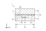
図1および図2を参照して、実施形態に係る非接触通信媒体の構成について説明する。図1は、実施形態に係る非接触通信媒体の平面図である。図2は、図1に示すII-II線矢視における断面図である。
<Configuration of non-contact communication medium>
A configuration of a non-contact communication medium according to an embodiment will be described with reference to Fig. 1 and Fig. 2. Fig. 1 is a plan view of the non-contact communication medium according to the embodiment. Fig. 2 is a cross-sectional view taken along line II-II in Fig. 1.
図1および図2に示すように、実施形態に係る非接触通信媒体1は、電子部品10と、収容体20とを有する。電子部品10は、たとえばRFIDタグである。
As shown in Figs. 1 and 2, the
RFIDとしての電子部品10は、たとえばLTCC(Low Temperature Co-fired Ceramics)等からなる基板上に、非接触通信用のアンテナと、このアンテナを介して非接触通信を行うICチップと、識別情報を記憶したメモリとを有する。RFIDとしての電子部品10は、電磁誘導、電波等を用いた非接触通信により、メモリに記憶された識別情報を外部機器(たとえば、RFIDリーダー)に送信することができる。
The
実施形態に係る非接触通信媒体1は、たとえば、電子部品10の耐熱温度を超える高温環境下において使用される。たとえば、実施形態に係る非接触通信媒体1は、めっき処理される部品に取り付けられ、この部品とともにめっき処理される。溶融亜鉛めっき等のめっき液の温度は、たとえば、75℃~500℃である。
The
また、実施形態に係る非接触通信媒体1は、部品とともに酸性の薬品やアルカリ性の薬品によって処理される場合がある。このように、実施形態に係る非接触通信媒体1は、電子部品10の耐薬品性を超える酸・アルカリ環境下において使用されることもある。
The
そこで、実施形態に係る非接触通信媒体1は、電子部品10を高温環境、酸・アルカリ環境から保護するために、電子部品10を封止する収容体20を有する。収容体20は、内部に収容空間25を有し、かかる収容空間25に電子部品10を収容する。
The
収容体20は、第1基材21および第2基材22と、接着層5とを有する。第1基材21および第2基材22は、接着層5を介して互いに接合される。
The
第1基材21および第2基材22は、比較的扁平な円柱形状を有する。具体的には、第1基材21および第2基材22は、平面視円形の2つの平坦面(上端面および下端面)を有するとともに、これら2つの平坦面を繋ぐ曲面(外周面)を有する。第1基材21の一方の平坦面21a(上端面)と第2基材22の一方の平坦面22a(下端面)とは、略同径で互いに対向しており、これらの間に接着層5が位置する。
The
第1基材21は、電子部品10を収容する収容凹部25aを有する。収容凹部25aは、平坦面21aの中央部に開口する。第1基材21と第2基材22とが接着層5を介して接合されることにより、第1基材21の平坦面21aは閉塞される。これにより、電子部品10は、収容体20の内部に封止される。
The
第1基材21および第2基材22は、セラミックスからなる。第1基材21および第2基材22を構成するセラミックスとしては、たとえばコージェライトを用いることができる。コージェライトは、熱膨張係数が小さいことから、耐熱衝撃性に優れており、また、熱伝導率が低いことから、電子部品10に熱を伝え難い。このように、コージェライトを使用することで、電子部品10を高温環境から適切に保護することができる。なお、第1基材21および第2基材22を構成するセラミックスは、必ずしもコージェライトであることを要しない。この点については、後述する。
The
接着層5は、第1基材21の平坦面21aと第2基材22の平坦面22aとの間に位置し、第1基材21と第2基材22とを接合する。接着層5は第2基材22の平坦面22aの全面に広がっている。このため、接着層5の一部は、収容空間25に面している。
The
本実施形態に係る接着層5は、端部5aにおける気孔率が内部5bにおける気孔率よりも低い。「気孔率が低い」とは、言い換えれば、接着層5が密であることを意味する。また、「気孔率が高い」とは、言い換えれば、接着層5が疎であることを意味する。
In this embodiment, the
接着層5の端部5aとは、接着層5のうち収容体20の外部に相対的に近い部位のことである。具体的には、接着層5の端部5aは、外部に露出しておりめっき液等に触れる可能性のある接着層5の端面を含む領域である。たとえば、接着層5の端部5aは、接着層5の端面から最大300μmまでの領域である。
The
接着層5の内部5bとは、接着層5のうち収容体20の収容空間25に相対的に近い部位のことである。具体的には、接着層5の内部5bは、接着層5の端部5aよりも収容体20の内側に位置する部位である。たとえば、接着層5の内部5bは、収容体20の内部に形成された収容空間25に面する領域であってもよい。
The interior 5b of the
このように、実施形態に係る接着層5は、「外側(端部5a)>内側(内部5b)」となる疎密差を有する。
In this way, the
この点について、図3を参照してさらに具体的に説明する。図3は、図2に示すH部の模式拡大図である。 This point will be explained in more detail with reference to Figure 3, which is a schematic enlarged view of part H shown in Figure 2.
図3に示すように、実施形態に係る接着層5は、接着剤51と封孔剤52とを有する。
As shown in FIG. 3, the
接着剤51は、非接触通信媒体1の使用環境に耐え得る耐熱性を有していればよい。このような接着剤としては、たとえば無機系の接着剤を用いることができる。また、接着剤としては、無機系の接着剤にセラミックス粉末を添加したものを用いてもよい。
The adhesive 51 only needs to have heat resistance sufficient to withstand the environment in which the
たとえば、接着剤51は、シリカを主成分とし、アルミナ、カルシア、ジルコン、ナトリウムガラス等を含有する。 For example, adhesive 51 is mainly composed of silica and contains alumina, calcia, zircon, sodium glass, etc.
接着剤51は、端部5aおよび内部5bを含む全領域に空隙511を有する。空隙511は、接着剤51の全領域にほぼ均等に分散している。
The adhesive 51 has
封孔剤52は、接着剤51の空隙511に入り込むことで、空隙511を塞ぐ。具体的には、封孔剤52は、接着剤51の全領域に分布する空隙511のうち端部5aに位置する空隙511を塞ぐ。
The
具体的には、封孔剤52は、微粒子とつなぎ剤とを含んでおり、微粒子が空隙511に入り込むとともに、空隙511に入り込んだ微粒子と接着剤51との間をつなぎ剤が繋ぐことで、空隙511を塞ぐことができる。製造工程上、封孔剤52には溶剤が含有されることが好ましい。溶剤を含有させることにより、接着剤51の内部へ微粒子およびつなぎ剤を浸透させやすくすることができる。なお、溶剤は、完成品には含まれていなくてもよい。なぜなら、溶剤は、製造の過程で空隙511から蒸発するからである。
Specifically, the
微粒子は、たとえばシリカ微粒子である。また、つなぎ剤は、たとえばシリコーンまたはエポキシである。耐熱性の観点から、つなぎ剤としては、シリコーンが用いられることが好ましい。なお、封孔剤52は、アルミナ、ジルコンを含有しない。
The fine particles are, for example, silica fine particles. The binder is, for example, silicone or epoxy. From the viewpoint of heat resistance, it is preferable to use silicone as the binder. The sealing
封孔剤52は、接着剤51の空隙511を塞ぐことができるものであればよく、上述した成分のものに限定されない。たとえば、封孔剤52としては、樹脂が用いられてもよい。
The
接着剤51の端部5aに位置する空隙511が封孔剤52によって塞がれることで、接着層5に「外側(端部5a)>内側(内部5b)」となる疎密差が形成される。すなわち、接着層5の端部5aにおける気孔率が、接着層5の内部5bにおける気孔率よりも低くなる。
The
収容体20の外部に相対的に近い接着層5の端部5aにおける気孔率が低い、言い換えれば、接着層5の端部5aが密であることで、収容体20の外部から収容空間25へのめっき液等の侵入を抑制することができる。また、収容体20の収容空間25に相対的に近い接着層5の内部5bにおける気孔率が高い、言い換えれば、接着層5の内部5bが疎であることで、接着層5の断熱性を向上させることができる。
The porosity of the
このように、実施形態に係る非接触通信媒体1によれば、収容体20の接合部分から外部の液体や気体が侵入することを抑制しつつ、電子部品10を高温環境から適切に保護することができる。
In this way, the
<製造方法>
次に、実施形態に係る非接触通信媒体1の製造方法の一例について説明する。
<Production Method>
Next, an example of a method for manufacturing the
まず、コージェライトの粉末および焼結助剤の粉末を準備する。焼結助剤は、たとえば、希土類酸化物(酸化イットリウム、酸化セリウムなど)、アルカリ金属酸化物(酸化リチウム、酸化ナトリウムなど)、アルカリ土類金属(酸化カルシウム)である。なお、コージェライトの粉末の代わりに、酸化マグネシウム、酸化アルミニウム、酸化珪素を所望のコージェライトの組成比に混合したものを用いてもよい。つづいて、準備した粉末を溶媒である水とともに振動ミルに投入して、粉砕・混合して原料を得る。 First, cordierite powder and sintering aid powder are prepared. The sintering aid is, for example, a rare earth oxide (yttrium oxide, cerium oxide, etc.), an alkali metal oxide (lithium oxide, sodium oxide, etc.), or an alkaline earth metal (calcium oxide). Note that instead of cordierite powder, a mixture of magnesium oxide, aluminum oxide, and silicon oxide in the desired cordierite composition ratio may be used. Next, the prepared powder is put into a vibration mill together with water as a solvent, and is pulverized and mixed to obtain the raw material.
つづいて、粉砕・混合して得られた原料に対し、バインダー、可塑剤および離型剤などの有機成分を添加した後、これらを撹拌することによってスラリーを作製し、作製したスラリーをスプレードライヤーを用いて噴霧乾燥することによってセラミックス顆粒を作製する。 Next, organic components such as binders, plasticizers, and release agents are added to the raw materials obtained by grinding and mixing, and then the mixture is stirred to produce a slurry. The slurry is then spray-dried using a spray dryer to produce ceramic granules.
つづいて、作製したセラミックス顆粒に対して粉末プレス成形を行って、第1基材21および第2基材22の成形体を得る。なお、収容凹部25aもこの工程において金型により成形される。
Next, the produced ceramic granules are powder-pressed to obtain the green bodies of the
つづいて、大気雰囲気中、真空雰囲気中または窒素ガス雰囲気中にて成形体を熱処理することにより脱脂を行った後、成形体の焼成を行うことにより、第1基材21および第2基材22が得られる。なお、所望の形状を得るために、第1基材21および第2基材22の成形体または焼成後の第1基材21および第2基材22に対して切削、研削工程を行ってもよい。
Then, the molded body is degreased by heat treatment in an air atmosphere, a vacuum atmosphere, or a nitrogen gas atmosphere, and then the molded body is fired to obtain the
つづいて、収容凹部25aに電子部品10を収容した後、第1基材21の平坦面21aおよび第2基材22の平坦面22aを接着剤51を用いて接合する。
Next, after the
その後、封孔剤52を接着剤51の端面(外周面)に塗布する。上述したように、浸透性を高める観点から、封孔剤52に溶剤を含有させてもよい。封孔剤52は、接着剤51の端部5aに位置する空隙511に入り込んで、空隙511を塞ぐ。これにより、接着層5に「外側(端部5a)>内側(内部5b)」の疎密差が形成される。以上により、実施形態に係る非接触通信媒体1が得られる。
Then, a sealing
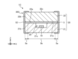
<第1変形例>
図4は、第1変形例に係る非接触通信媒体の拡大断面図である。また、図5は、第1変形例に係る被覆層の他の例を示す図である。
<First Modification>
Fig. 4 is an enlarged cross-sectional view of the non-contact communication medium according to the first modified example, and Fig. 5 is a diagram showing another example of the covering layer according to the first modified example.
図4に示すように、第1変形例に係る非接触通信媒体1Aは、被覆層30Aをさらに有する。被覆層30Aは、第1基材21と第2基材22との間の領域、すなわち、接着層5が介在する領域の外に位置しており、接着層5の端部5aを覆う。
As shown in FIG. 4, the
具体的には、第1変形例に係る被覆層30Aは、接着層5の端部5aを覆うとともに、収容体20の外面のうち接着層5の端部5aが露出する露出面、ここでは、第1基材21および第2基材22の外周面21b,22bの一部も覆っている。
Specifically, the
第1変形例において、被覆層30Aは、封孔剤52からなる。また、図5に示すように、被覆層30Aは、接着剤51と封孔剤52とからなっていてもよい。この場合、接着層5に近い側に接着剤51が位置し、その外側に封孔剤52が位置していればよい。被覆層30Aに含まれる接着剤51の空隙511(ここでは、図示せず)に封孔剤52が入り込むことで、被覆層30Aに含まれる接着剤51の気孔率は、接着層5の端部5aにおける気孔率以下となっている。なお、図5では、接着剤51と封孔剤52とが明確に分離している場合の例を示したが、接着剤51と封孔剤52とは混在していてもよい。
In the first modified example, the
このように、接着層5の端部5aにおける気孔率と同程度の気孔率を有する被覆層30Aで接着層5の外側を覆うことにより、収容空間25へのめっき液等の侵入をさらに抑制することができる。
In this way, by covering the outside of the
<第2変形例>
図6は、第2変形例に係る非接触通信媒体の拡大断面図である。また、図7は、第2変形例に係る被覆層の他の例を示す図である。
<Second Modification>
Fig. 6 is an enlarged cross-sectional view of the non-contact communication medium according to the second modified example, and Fig. 7 is a diagram showing another example of the covering layer according to the second modified example.
図6に示すように、第2変形例に係る非接触通信媒体1Bは、被覆層30Bをさらに有する。被覆層30Bは、たとえば封孔剤52からなる。
As shown in FIG. 6, the
第2変形例に係る被覆層30Bは、接着層5の端部5aを覆うとともに、第1基材21および第2基材22の外周面21b,22bの全面を覆っている。
The
このように、被覆層30Bは、第1基材21および第2基材22の外周面21b,22bの全体に広がっていてもよい。これにより、収容空間25へのめっき液等の侵入をより確実に抑制することができる。
In this way, the
図7に示すように、被覆層30Bは、接着剤51と封孔剤52とからなっていてもよい。この場合、接着層5に近い側に接着剤51が位置し、その外側に封孔剤52が位置していればよい。被覆層30Bに含まれる接着剤51の空隙511(ここでは図示せず)に封孔剤52が入り込むことで、被覆層30Bに含まれる接着剤51の気孔率は、接着層5の端部5aにおける気孔率以下となっている。なお、図7では、接着剤51と封孔剤52とが明確に分離している場合の例を示したが、接着剤51と封孔剤52とは混在していてもよい。
As shown in FIG. 7, the
このように、第1基材21および第2基材22の外周面21b,22bの全面を接着剤51で覆うことにより、収容体20の耐熱性および耐薬品性を向上させることができる。
In this way, by covering the entire
<第3変形例>
図8は、第3変形例に係る非接触通信媒体の拡大断面図である。また、図9は、第3変形例に係る被覆層の他の例を示す図である。
<Third Modification>
Fig. 8 is an enlarged cross-sectional view of the non-contact communication medium according to the third modified example, and Fig. 9 is a diagram showing another example of the covering layer according to the third modified example.
図8に示すように、第3変形例に係る非接触通信媒体1Cは、被覆層30Cをさらに有する。被覆層30Cは、たとえば封孔剤52からなる。
As shown in FIG. 8, the
第3変形例に係る被覆層30Cは、接着層5の端部5aを覆うとともに、第1基材21および第2基材22の外周面21b,22bの全面を覆っている。さらに、第3変形例に係る被覆層30Cは、第1基材21の外周面21bに連続する第1基材21の下端面21cの外周部を含む一部と、第2基材22の外周面22bに連続する第2基材22の上端面22cの外周部を含む一部とを覆っている。
The
このように、被覆層30Cは、収容体20の外面のうち第1基材21および第2基材22の外周面21b,22bに連続する他の面(下端面21cおよび上端面22c)の一部に広がっていてもよい。これにより、収容空間25へのめっき液等の侵入をより確実に抑制することができる。
In this way, the
図9に示すように、被覆層30Cは、接着剤51と封孔剤52とからなっていてもよい。この場合、被覆層30Cの接着剤51は、第1基材21および第2基材22の外周面21b,22bにのみ位置していてもよい。
As shown in FIG. 9, the
<第4変形例>
図10は、第4変形例に係る非接触通信媒体の拡大断面図である。また、図11は、第4変形例に係る被覆層の他の例を示す図である。
<Fourth Modification>
Fig. 10 is an enlarged cross-sectional view of a non-contact communication medium according to the fourth modified example, and Fig. 11 is a diagram showing another example of a covering layer according to the fourth modified example.
図10に示すように、第4変形例に係る非接触通信媒体1Dは、被覆層30Dをさらに有する。被覆層30Dは、たとえば封孔剤52からなる。
As shown in FIG. 10, the
第4変形例に係る被覆層30Dは、収容体20の全面を覆っている。このように、収容体20の全体を被覆層30Dで覆うことで、収容空間25へのめっき液等の侵入をより確実に抑制することができる。
The
図11に示すように、被覆層30Dは、接着剤51と封孔剤52とからなっていてもよい。この場合、被覆層30Dの接着剤51は、第1基材21および第2基材22の外周面21b,22bにのみ位置していてもよい。
As shown in FIG. 11, the
<第5変形例>
図12は、第5変形例に係る非接触通信媒体の断面図である。図12に示す非接触通信媒体1Eの収容体20Eは、第1基材21と第2基材22との間で、且つ、接着層5Eの外側に、緻密部材40を有する。
<Fifth Modification>
Fig. 12 is a cross-sectional view of a non-contact communication medium according to a fifth modified example. A
緻密部材40は、接着層5Eの端部5aにおける気孔率よりも低い気孔率を有するもの、すなわち、接着層5Eの端部5aよりも緻密なものであればよい。たとえば、緻密部材40は、上述した封孔剤52であってもよい。また、緻密部材40は、PEEK(ポリエーテルエーテルケトン)、ポリイミド、シリコーンなどの耐熱性を有する樹脂であってもよい。
The
このように、非接触通信媒体1Eは、第1基材21と第2基材22との間で、且つ、接着層5Eの外側に緻密部材40を有していてもよい。接着層5Eの外側を緻密部材40で覆うことで、収容空間25へのめっき液等の侵入をより確実に抑制することができる。また、第1基材21と第2基材22との間に緻密部材40を位置させることで、収容体20Eの凹凸を少なくすることができるため、収容体20Eの欠けや割れなどの損傷を抑制することができる。
In this way, the
<第6変形例>
図13は、第6変形例に係る非接触通信媒体の平面図である。また、図14は、図13に示すXIV-XIV線矢視における断面図である。
<Sixth Modification>
Fig. 13 is a plan view of a non-contact communication medium according to a sixth modified example, and Fig. 14 is a cross-sectional view taken along line XIV-XIV in Fig. 13.
図13および図14に示すように、第6変形例に係る非接触通信媒体1Hは、収容体20Hを有する。
As shown in Figures 13 and 14, the
第6変形例に係る収容体20Hは、セラミックスからなる第1基材21Hおよび第2基材22と、接着層5Hとを有しており、第1基材21Hと第2基材22とは、接着層5Hを介して互いに接合される。
The
第1基材21Hは、円柱形状を有しており、両端に平面視円形の平坦面(上端面および下端面)を有するとともに、これら両端面を繋ぐ曲面(外周面)を有する。
The
第1基材21Hの一方の端面(以下、第1平坦面211と記載する)には、電子部品10が収容される収容穴25Haが開口している。収容穴25Haは、第1平坦面211の中央部に開口し、第1平坦面211に対して垂直に延在する。収容穴25Haは、平面視円形状を有する。
One end face of the
第2基材22Hは、円柱形状を有しており、両端に平面視円形の平坦面(上端面および下端面)を有するとともに、これら両端面を繋ぐ曲面(外周面)を有する。第2基材22Hの平面形状は、収容穴25Haの平面形状と同一の円形であり、且つ、収容穴25Haの平面形状よりも小径である。
The
かかる第2基材22Hは、収容穴25Haに挿入される。収容穴25Haに挿入された状態において、第2基材22Hの一方の端面(以下、第2平坦面221と記載する)は、第1基材21Hの第1平坦面211と面一となる。このように、第2基材22Hは、収容穴25Haに対して入れ子状に内挿される。
Such
接着層5Hは、収容穴25Haの内周面251と第2基材22Hの外周面222との間に位置し、第1基材21Hと第2基材22Hとを接合する。これにより、収容穴25Haは、第2基材22および接着層5Hによって閉塞され、収容穴25Haに収容された電子部品10が封止される。第2基材22Hおよび接着層5Hによって閉塞された収容穴25Haの内部は収容空間25Hとなっており、電子部品10は、第2基材22Hおよび接着層5Hから離れた位置に配置される。
The
このように、実施形態に係る非接触通信媒体1Hは、収容穴25Haを第2基材22Hで閉塞することにより、収容穴25Ha内の電子部品10を封止する構造を有する。かかる非接触通信媒体1Hにおいて、第1基材21Hと第2基材22Hとを接合する接着層5Hは、収容穴25Haの内周面と第2基材22の外周面と間、すなわち、収容穴25Ha内に位置している。すなわち、収容体20Hの接合部分である接着層5Hが外部にほとんど露出していない。したがって、実施形態に係る非接触通信媒体1Hによれば、収容体20Hの接合部分の剥がれが生じにくい。
In this way, the
かかる非接触通信媒体1Hにおいて、接着層5Hは、収容体20Hの外部に相対的に近い端部5Haにおける気孔率が、収容空間25Hに相対的に近い内部5Hbにおける気孔率よりも低い。これにより、収容体20Hの接合部分から外部の液体や気体が侵入することを抑制することができる。また、電子部品10を高温環境から適切に保護することができる。
In such a
非接触通信媒体1Hは、上述した第1~第5変形例と同様に、被覆層を有していてもよい。すなわち、非接触通信媒体1Hは、接着層5Hの端部5Haを覆う被覆層を有していてもよい。この被覆層は、接着層5Hだけでなく、第1平坦面211および第2平坦面221の一部または全部を覆っていてもよい。また、被覆層は、第1基材21Hの外周面の一部または全部をさらに覆っていてもよい。
The
<第7変形例>
以下に示す第7~第10変形例では、収容体が3つ以上の基材で構成される場合の例について説明する。まず、第7変形例について図15および図16を参照して説明する。図15は、第7変形例に係る非接触通信媒体の平面図である。また、図16は、図15に示すXVI-XVI線矢視における断面図である。
<Seventh Modification>
In the seventh to tenth modified examples shown below, examples in which the container is composed of three or more base materials will be described. First, the seventh modified example will be described with reference to Fig. 15 and Fig. 16. Fig. 15 is a plan view of a non-contact communication medium according to the seventh modified example. Fig. 16 is a cross-sectional view taken along the line XVI-XVI shown in Fig. 15.
図15および図16に示すように、第7変形例に係る非接触通信媒体1Jは、電子部品10と、収容体20Jとを有する。電子部品10は、たとえばRFIDタグである。
As shown in Figs. 15 and 16, the
第7変形例に係る収容体20Jは、第1基材21Jと第2基材22Jと第3基材23Jと、2つの接着層5Jとを有する。図16に示す例において、第1基材21J、第2基材22Jおよび第3基材23Jは、下から順に、第3基材23J、第1基材21Jおよび第2基材22Jの順番で積層される。
The
第1基材21Jは、比較的扁平な円筒形状を有する。具体的には、第1基材21Jは、第1基材21Jを上下に貫通する貫通孔25Jaを有する。また、第2基材22Jおよび第3基材23Jは、比較的扁平な円柱形状を有する。
The
第1基材21Jおよび第2基材22Jは、接着層5Jを介して互いに接合される。同様に、第2基材22Jおよび第3基材23Jとは、接着層5Jを介して互いに接合される。これにより、第1基材21Jの貫通孔25Jaが塞がれることで、収容体20Jの内部に電子部品10の収容空間25Jが形成される。
The
このように、収容体20Jは、3つの基材21J~23Jを接着層5Jで接合することによって形成されてもよい。3つ以上の基材21J~23Jを積層することで、収容体20Jを基材21J~23Jの積層方向に厚くすることができる。これにより、たとえば、収容体20Jの耐熱性および耐薬品性等を向上させることができる。
In this manner, the
<第8変形例>
図17は、第8変形例に係る非接触通信媒体の断面図である。図17に示すように、第8変形例に係る非接触通信媒体1Kの収容体20Kは、第1基材21Kを有する。
<Eighth Modification>
Fig. 17 is a cross-sectional view of a non-contact communication medium according to Modification Example 8. As shown in Fig. 17, a
第1基材21Kは、たとえば第2基材22Jとの対向面(上端面)に、貫通孔25Jaを囲む環状の凹部25Jbを有していてもよい。凹部25Jbは、たとえば、外部から侵入してきためっき液等を溜める空間として機能する。これにより、収容体20Kの接合部分から外部の液体や気体が収容空間25Jに到達することを抑制することができる。
The
なお、凹部25Jbは、必ずしも周状であることを要しない。たとえば、第1基材21Kは、平面視円形の複数の凹部を有していてもよく、これら複数の凹部が周状に並べられていてもよい。
Note that the recesses 25Jb do not necessarily have to be circumferential. For example, the
また、ここでは、凹部25Jbが第1基材21Kに設けられる場合の例を示したが、凹部25Jbは、第2基材22または第3基材23Jに設けられてもよい。
In addition, while an example is shown here in which the recess 25Jb is provided in the
<第9変形例>
図18は、第9変形例に係る非接触通信媒体の断面図である。図18に示すように、第9変形例に係る非接触通信媒体1Lの収容体20Lは、第1基材21Lを有する。
<Ninth Modification>
Fig. 18 is a cross-sectional view of a non-contact communication medium according to a ninth modification. As shown in Fig. 18, a
第9変形例に係る第1基材21Lは、同心円状に配置された2つの円筒状部材からなる。具体的には、第1基材21Lは、第1円筒部材21L1と、第1円筒部材21L1の外側に位置する第2円筒部材21L2とを有する。第1円筒部材21L1は、電子部品10の収容空間25Jとなる第1貫通孔25Laを有する。また、第2円筒部材21L2は、第2貫通孔25Lbを有する。
The
かかる第1基材21Lを有する収容体20Lは、第1円筒部材21L1と第2円筒部材21L2との間に隙間を有する。この隙間は、上述した凹部25Jbと同様、たとえば、外部から侵入してきためっき液等を溜める空間として機能する。これにより、収容体20Lの接合部分から外部の液体や気体が収容空間25Jに到達することを抑制することができる。
The
<第10変形例>
図19は、第10変形例に係る非接触通信媒体の断面図である。図19に示すように、第10変形例に係る非接触通信媒体1Mの収容体20Mは、第2基材22Mおよび第3基材23Mを有する。
<Tenth Modification>
Fig. 19 is a cross-sectional view of a non-contact communication medium according to
第10変形例に係る第2基材22Mは、第1基材21Jとの対向面(下端面)に凹部22Maを有する。凹部22Maは、第1基材21Jと第2基材22Mとが接合された場合に、第1基材21Jの貫通孔25Jaと連通する。
The
同様に、第10変形例に係る第3基材23Mは、第1基材21Jとの対向面(上端面)に凹部23Maを有する。凹部23Maは、第1基材21Jと第3基材23Mとが接合された場合に、第1基材21Jの貫通孔25Jaと連通する。
Similarly, the
このように、第1基材21Jの貫通孔25Jaと連通する凹部22Ma,23Maを第2基材22Mおよび第3基材23Mに設けることで、電子部品10の収容空間25Jを広くすることができる。これにより、たとえば、電子部品10に外部からの熱を伝え難くすることができる。なお、凹部22Ma,23Maは、必ずしも第2基材22Mおよび第3基材23Mに形成されることを要しない。凹部22Ma,23Maは、第2基材22Mおよび第3基材23Mのうち一方にのみ形成されてもよい。
In this way, by providing the recesses 22Ma, 23Ma in the
上述した第6~第10変形例において、電子部品10の収容空間25Jは、たとえば多孔体等によって埋まっていてもよい。第8変形例に係る凹部25Jb、第9変形例に係る第1円筒部材21L1と第2円筒部材21L2との間の隙間についても同様である。
In the sixth to tenth modified examples described above, the
上述した第6~第10変形例において、接着層5Jは、「外側>内側」となる疎密差を有していてもよい。すなわち、接着層5Jは、端部における気孔率が内部における気孔率よりも低くてもよい。
In the sixth to tenth modified examples described above, the
上述した第6~第10変形例では、収容体が3つの基材を有する場合の例について説明したが、収容体は、4つ以上の基材を積層することにより構成されてもよい。 In the sixth to tenth modified examples described above, examples were described in which the container has three base materials, but the container may also be formed by stacking four or more base materials.
<第11変形例>
図20は、第11変形例に係る非接触通信媒体の斜視図である。また、図21は、第11変形例に係る非接触通信媒体の断面図である。
<Eleventh Modification>
Fig. 20 is a perspective view of a non-contact communication medium according to an eleventh modified example, and Fig. 21 is a cross-sectional view of the non-contact communication medium according to the eleventh modified example.
図20に示すように、第11変形例に係る非接触通信媒体1Nは、収容体20Nを有する。収容体20Nは、第1基材21Nと、第2基材22Nと、接着層5Nとを有する。
As shown in FIG. 20, the
第1基材21Nは、比較的扁平な円柱形状を有する。具体的には、第1基材21Nは、平面視円形の2つの平坦面(上端面および下端面)を有するとともに、これら2つの平坦面を繋ぐ曲面(外周面)を有する。
The
より具体的には、第1基材21Nは、第1の第1基材21N1と、第2の第1基材21N2とを有する。第1の第1基材21N1および第2の第1基材21N2は、比較的扁平な円柱形状を有する。
More specifically, the
第1の第1基材21N1と第2の第1基材21N2とは、第1の第1基材21N1の下端面215と、第2の第1基材21N2の上端面216とにおいて接合される。第1の第1基材21N1と第2の第1基材21N2との接合は、たとえば、第1の第1基材21N1および第2の第1基材21N2の成形体または焼結体同士を重ねて焼成した際に、粒界中のガラス成分が互いに融合して固着することによって行われる。なお、第1の第1基材21N1の下端面215と、第2の第1基材21N2の上端面216とは、たとえば接着層によって接合されてもよい。
The first first substrate 21N1 and the second first substrate 21N2 are joined at the
第1基材21Nは、第1基材21Nの外周面から第1基材21Nの内部に向かって延在する収容穴25Nを有する。収容穴25Nは、第1の第1基材21N1の下端面215に位置する第1溝部217と、第2の第1基材21N2の上端面216に位置する第2溝部218とによって構成される。
The
具体的には、第1溝部217は、たとえば、第1の第1基材21N1の外縁から中心部に向かって延在する。第1溝部217の延在方向に沿って第1溝部217を見たとき、第1溝部217は、たとえば、半円形状を有している。また、第2溝部218は、第2の第1基材21N2の外縁から中心部に向かって延在する。第2溝部218の延在方向に沿って第2溝部218を見たとき、第2溝部218は、たとえば、半円形状を有している。そして、これら第1溝部217と第2溝部218とによって構成される収容穴25Nは、第1基材21Nの外周面から第1基材21Nの内部(中心部)に向かって延在する円筒状の空間となる。かかる収容穴25Nには、電子部品10が収容される。
Specifically, the
第2基材22Nは、円柱形状を有している。具体的には、第2基材22Nは、両端に平面視円形の平坦面(図21における左右両端面)を有するとともに、これら両端面を繋ぐ曲面(外周面)を有する。第2基材22Nの平面形状は、収容穴25Nの平面形状と同一の円形であり、且つ、収容穴25Nの平面形状よりも小径である。
The
第2基材22Nは、収容穴25Nに挿入される。収容穴25Nに挿入された状態において、第2基材22Nの一方の端面(以下、第1平坦面225と記載する)は、たとえば、第1基材21Nの外周面と面一となる。このように、第2基材22Nは、収容穴25Nに対して入れ子状に内挿される。
The
接着層5Nは、収容穴25Nの内周面と第2基材22Nの外周面との間に位置し、第1基材21Nと第2基材22Nとを接合する。これにより、収容穴25Nは、第2基材22Nおよび接着層5Nによって閉塞され、収容穴25Nに収容された電子部品10が封止される。第2基材22Nおよび接着層5Nによって閉塞された収容穴25Nの内部は収容空間となっており、電子部品10は、第2基材22Nおよび接着層5Nから離れた位置に配置される。
The
このように、実施形態に係る非接触通信媒体1Nは、収容穴25Nを第2基材22Nで閉塞することにより、収容穴25N内の電子部品10を封止する構造を有する。かかる非接触通信媒体1Nにおいて、第1基材21Nと第2基材22Nとを接合する接着層5Nは、収容穴25Nの内周面と第2基材22の外周面と間、すなわち、収容穴25N内に位置している。つまり、収容体20Nの接合部分である接着層5Nが外部にほとんど露出していない。したがって、実施形態に係る非接触通信媒体1Nによれば、収容体20Nの接合部分の剥がれが生じにくい。
In this way, the
非接触通信媒体1Nにおいて、接着層5Nは、収容体20Nの外部に相対的に近い端部における気孔率が、収容穴25Nに相対的に近い内部における気孔率よりも低くてもよい。これにより、収容体20Nの接合部分から外部の液体や気体が侵入することを抑制することができる。また、電子部品10を高温環境から適切に保護することができる。また、非接触通信媒体1Nは、被覆層を有していてもよい。すなわち、非接触通信媒体1Nは、少なくとも接着層5Nの端部を覆う被覆層を有していてもよい。
In the
<第12変形例>
図22は、第12変形例に係る収容穴を収容穴の延在方向に沿って見た図である。なお、第12変形例に係る非接触通信媒体1Pの構成のうち収容穴25P以外の構成については、第11変形例に係る非接触通信媒体1Nの構成と同様である。
<Twelfth Modification>
22 is a view of the accommodation hole according to the 12th modification seen along the extension direction of the accommodation hole. Note that the configuration of the
図22に示すように、第12変形例に係る非接触通信媒体1Pが有する収容穴25Pは、第1の第1基材21P1の第1溝部217と第2の第1基材21P2の第2溝部218とが、第1基材21Pの周方向にずれた形状であってもよい。かかる構成によれば、接着層5Pによる接合領域が増加することから、第1基材21Pと第2基材22Pとをより強固に接合することができる。したがって、第12変形例に係る非接触通信媒体1Pによれば、信頼性を高めることができる。
As shown in FIG. 22, the
非接触通信媒体1Pは、被覆層を有していてもよい。すなわち、非接触通信媒体1Pは、少なくとも接着層5Pの端部を覆う被覆層を有していてもよい。
The
<第13変形例>
図23は、第13変形例に係る非接触通信媒体の断面図である。なお、第13変形例に係る非接触通信媒体1Qの構成のうち収容穴25Q以外の構成については、第11変形例に係る非接触通信媒体1Nの構成と同様である。
<Thirteenth Modification>
23 is a cross-sectional view of a non-contact communication medium according to the 13th modification. The configuration of the
図23に示すように、第13変形例に係る非接触通信媒体1Qは、第1基材21Qと、第2基材22Qと、接着層(ここでは、図示せず)とを有する。
As shown in FIG. 23, the
第13変形例に係る非接触通信媒体1Qが有する収容穴25Qは、延在方向における底部に段差255を有していてもよい。たとえば、第1の第1基材21Q1の第1溝部217を、第2の第1基材21Q2の第2溝部218よりも長く形成することで段差255を有する収容穴25Qを得ることができる。第2溝部218を第1溝部217よりも長く形成した場合も同様である。また、第1の第1基材21Q1と第2の第1基材21Q2とを第1溝部217および第2溝部218の延在方向に沿ってずらした状態で接合してもよい。この場合にも、段差255を有する収容穴25Qを得ることができる。
The
このように、収容穴25Qの底部に段差255を設けることで、電子部品10が第1基材21Qに対して面接触し難くなるため、電子部品10と第1基材21Qとの接触面積を少なくすることができる。これにより、電子部品10に対して熱が伝わりにくくなることから、非接触通信媒体1Qの信頼性を高めることができる。
In this way, by providing a
非接触通信媒体1Qは、被覆層を有していてもよい。すなわち、非接触通信媒体1Qは、少なくとも接着層(ここでは、図示せず)の端部を覆う被覆層を有していてもよい。
The
<第14変形例>
図24は、第14変形例に係る非接触通信媒体の断面図である。また、図25は、第14変形例に係る第1基材の平面図である。なお、図24に示す断面図は、図25に示すXXIV-XXIV線矢視における断面図である。また、第14変形例に係る非接触通信媒体1Rの構成のうち第1基材21R以外の構成については、実施形態に係る非接触通信媒体1の構成と同様である。
<Fourteenth Modification>
Fig. 24 is a cross-sectional view of a non-contact communication medium according to the fourteenth modification. Fig. 25 is a plan view of a first substrate according to the fourteenth modification. The cross-sectional view shown in Fig. 24 is a cross-sectional view taken along the arrows XXIV-XXIV shown in Fig. 25. The configuration of the
図24に示すように、第14変形例に係る非接触通信媒体1Rが有する収容体20Rは、第1基材21Rと、第2基材22Rと、接着層5Rとを有する。第1基材21Rおよび第2基材22Rは、接着層5Rを介して互いに接合される。
As shown in FIG. 24, the
第1基材21Rの平坦面21a(上端面)には、収容凹部25aが位置している。収容凹部25aは、平坦面21aの中央部に開口する。第1基材21Rと第2基材22Rとが接着層5Rを介して接合されることにより、第1基材21Rの平坦面21aは閉塞される。これにより、密閉された収容空間25Rが形成される。電子部品10は、かかる収容空間25Rに封止される。
A
第1基材21Rの平坦面21aには、さらに、複数の凸部26が位置している。図25に示すように、複数の凸部26は、たとえば、収容凹部25aを囲むように周状に並べられている。ここでは、第1基材21Rの平坦面21aに4つの凸部26が位置する場合の例を示しているが、凸部26の数は5つ以上であってもよい。また、凸部26の数は、3つ以下であってもよい。また、複数の凸部26は、必ずしも周状に設けられることを要しない。
Furthermore, a plurality of
また、ここでは、複数の凸部26が接着層5Rの端部5aよりも収容体20Rの内側に位置する場合の例を示したが、複数の凸部26は、接着層5Rの端部5aに位置していてもよい。また、複数の凸部26は、第2基材22Rの平坦面22aに位置していてもよい。
In addition, although an example is shown here in which the
このように、第14変形例に係る非接触通信媒体1Rは、複数の凸部26を有する。かかる場合、接着層5Rを介した非接触通信媒体1Rの外部から内部への熱の移動を凸部26によって阻害することができる。したがって、第14変形例に係る非接触通信媒体1Rによれば、断熱効果を高めることができる。また、クラックの進展を抑制することができる。
In this way, the
非接触通信媒体1Rは、被覆層を有していてもよい。すなわち、非接触通信媒体1Rは、少なくとも接着層5Rの端部を覆う被覆層を有していてもよい。
The
<第15変形例>
図26は、第15変形例に係る非接触通信媒体の拡大断面図である。図26に示すように、第15変形例に係る非接触通信媒体1Sが有する収容体20Sは、第1基材21Sと、第2基材22Sと、接着層5Sとを有する。
<Fifteenth Modification>
Fig. 26 is an enlarged cross-sectional view of a non-contact communication medium according to Modification 15. As shown in Fig. 26, a
第1基材21Sが有する凸部26Sは、断面視において湾曲した凸形状を有する。また、第2基材22Sは、平坦面22aにおける凸部26Sと対向する位置に凹部27Sを有する。
The
図26に示す断面視、具体的には、第1基材21Sの平坦面21aおよび第2基材22Sの22aに垂直かつ平坦面21a,22aの中心を通る面で収容体20Sを切断した断面視において、凹部27Sの幅W1は、凸部26Sの幅W2よりも小さい。この場合、凸部26Sは、凹部27Sの開口端27S1に接触して凹部27Sを閉塞する。凸部26Sによって閉塞された凹部27Sの内部空間27S2は、接着剤が充填されていない空洞を有していてもよい。
In the cross-sectional view shown in FIG. 26, specifically, in a cross-sectional view of the
このように、凹部27Sの幅を凸部26Sの幅よりも小さくすることで、凹部27Sと凸部26Sとの間に内部空間27S2を形成することができる。かかる場合、内部空間27S2が断熱層となることで、接着層5Sを介した非接触通信媒体1Sの外部から内部への熱の移動を阻害することができる。したがって、第15変形例に係る非接触通信媒体1Sによれば、断熱効果をさらに高めることができる。また、クラックの進展をさらに抑制することができる。
In this way, by making the width of the
また、第15変形例に係る非接触通信媒体1Sによれば、凹部27Sの位置は、凸部26Sの位置と対応していることから、非接触通信媒体1Sの製造工程において、第1基材21Sと第2基材22Sとの位置合わせを容易化することができる。
In addition, in the
非接触通信媒体1Sは、被覆層を有していてもよい。すなわち、非接触通信媒体1Sは、少なくとも接着層5Sの端部を覆う被覆層を有していてもよい。
The
<第16変形例>
図27は、第16変形例に係る非接触通信媒体の拡大断面図である。図27に示すように、第16変形例に係る非接触通信媒体1Tが有する収容体20Tは、第1基材21Tと、第2基材22Tと、接着層5Tとを有する。
<16th Modification>
Fig. 27 is an enlarged cross-sectional view of a non-contact communication medium according to Modification 16. As shown in Fig. 27, a
第1基材21Tが有する凸部26Tは矩形状であり、先端面は平坦である。一方、第2基材22Tが有する凹部27Tの内面は湾曲している。また、第2基材22Tが有する凹部27Tの幅W1は、凸部26Tの幅W2よりも大きい。
The
この場合、凹部27Tの湾曲した内面に凸部26Tが接触して凹部27Tを閉塞する。凸部26Tによって閉塞された凹部27Tの内部空間27T2は、接着剤が充填されていない空洞を有していてもよい。かかる場合、内部空間27T2が断熱層となることで、接着層5Tを介した非接触通信媒体1Tの外部から内部への熱の移動を阻害することができる。したがって、第16変形例に係る非接触通信媒体1Tによれば、断熱効果をさらに高めることができる。また、クラックの進展をさらに抑制することができる。
In this case, the
また、第16変形例に係る非接触通信媒体1Tによれば、凹部27Tの位置は、凸部26Tの位置と対応していることから、非接触通信媒体1Tの製造工程において、第1基材21Tと第2基材22Tとの位置合わせを容易化することができる。
In addition, in the
非接触通信媒体1Tは、被覆層を有していてもよい。すなわち、非接触通信媒体1Tは、少なくとも接着層5Tの端部を覆う被覆層を有していてもよい。
The
<第17変形例>
図28は、第17変形例に係る非接触通信媒体の拡大断面図である。図28に示すように、第17変形例に係る非接触通信媒体1Uが有する収容体20Uは、第1基材21Uと、第2基材22Uと、接着層5Uとを有する。
<Seventeenth Modification>
Fig. 28 is an enlarged cross-sectional view of a non-contact communication medium according to Modification 17. As shown in Fig. 28, a
第1基材21Uが有する凸部26Uおよび第2基材22Uが有する凹部27Uは、断面視において湾曲した凹形状を有する。また、凹部27Uの幅W1は、凸部26Uの幅W2よりも大きい。この場合、凸部26Uは、凹部27Uに接触する。
The
このように、第1基材21Uと第2基材22Uとの間には、必ずしも内部空間(空洞)が位置していることを要しない。かかる場合であっても、接着層5Uを介した非接触通信媒体1Uの外部から内部への熱の移動を凸部26Uによって阻害することができる。したがって、第17変形例に係る非接触通信媒体1Uによれば、断熱効果を高めることができる。また、クラックの進展を抑制することができる。また、第17変形例に係る非接触通信媒体1Uによれば、非接触通信媒体1Uの製造工程において、第1基材21Uと第2基材22Uとの位置合わせを容易化することができる。
In this way, it is not necessary that an internal space (cavity) is located between the
非接触通信媒体1Uは、被覆層を有していてもよい。すなわち、非接触通信媒体1Uは、少なくとも接着層5Uの端部を覆う被覆層を有していてもよい。
The
<第18変形例>
図29は、第18変形例に係る非接触通信媒体の拡大断面図である。図29に示すように、第18変形例に係る非接触通信媒体1Vが有する収容体20Vは、第1基材21Vと、第2基材22Vと、接着層5Vとを有する。
<18th Modification>
Fig. 29 is an enlarged cross-sectional view of a non-contact communication medium according to Modification 18. As shown in Fig. 29, a
第1基材21Vが有する凸部26Vおよび第2基材22Vが有する凹部27Vは、断面視において湾曲した凹形状を有する。第2基材22Vが有する凹部27Vの幅は、第1基材21Vが有する凸部26Vの幅と同一である。また、凹部27Vの深さは、凸部26Vの突出高さと同一である。
The
第18変形例に係る非接触通信媒体1Vにおいて、凸部26Vは、凹部27Vに接触しておらず、凸部26Vと凹部27Vとの間には接着層5Vが介在する。このように、凸部26Vは必ずしも第2基材22Vに接触していることを要しない。かかる場合であっても、接着層5Vを介した非接触通信媒体1Vの外部から内部への熱の移動を凸部26Vによって阻害することができる。したがって、第18変形例に係る非接触通信媒体1Vによれば、断熱効果を高めることができる。また、クラックの進展を抑制することができる。また、第18変形例に係る非接触通信媒体1Vによれば、非接触通信媒体1Vの製造工程において、第1基材21Vと第2基材22Vとの位置合わせを容易化することができる。
In the
非接触通信媒体1Vは、被覆層を有していてもよい。すなわち、非接触通信媒体1Vは、少なくとも接着層5Vの端部を覆う被覆層を有していてもよい。
The
<第19変形例>
図30は、第19変形例に係る非接触通信媒体の断面図である。また、図31は、第19変形例に係る第1基材の平面図である。なお、図31に示す断面図は、図30に示すXXXI-XXXI線矢視における断面図である。また、第19変形例に係る非接触通信媒体1Wの構成のうち第1基材21W以外の構成については、実施形態に係る非接触通信媒体1の構成と同様である。
<Nineteenth Modification>
Fig. 30 is a cross-sectional view of a non-contact communication medium according to the 19th modified example. Fig. 31 is a plan view of a first substrate according to the 19th modified example. The cross-sectional view shown in Fig. 31 is a cross-sectional view taken along the arrows of line XXXI-XXXI shown in Fig. 30. The configuration of the
図30に示すように、第19変形例に係る非接触通信媒体1Wが有する収容体20Wは、第1基材21Wと、第2基材22Wと、接着層5Wとを有する。第1基材21Wおよび第2基材22Wは、接着層5Wを介して互いに接合される。
As shown in FIG. 30, the
第1基材21Wの平坦面21a(上端面)には、収容凹部25aが位置している。収容凹部25aは、平坦面21aの中央部に開口する。第1基材21Wと第2基材22Wとが接着層5Wを介して接合されることにより、第1基材21Wの平坦面21aは閉塞される。これにより、密閉された収容空間25Wが形成される。電子部品10は、かかる収容空間25Wに封止される。
An
第1基材21Wの平坦面21aには、さらに、複数の凹部28が位置している。図31に示すように、複数の凹部28は、たとえば、収容凹部25aを囲むように周状に並べられている。ここでは、第1基材21Wの平坦面21aに4つの凹部28が位置する場合の例を示しているが、凹部28の数は5つ以上であってもよい。また、凹部28の数は、3つ以下であってもよい。
Furthermore, a plurality of
また、複数の凹部28は、必ずしも周状に設けられることを要しない。また、ここでは、複数の凹部28が接着層5Wの端部5aよりも収容体20Wの内側に位置する場合の例を示したが、複数の凹部28は、接着層5Wの端部5aに位置していてもよい。また、複数の凹部28は、第2基材22Wの平坦面22aに位置していてもよい。
The
このように、第19変形例に係る非接触通信媒体1Wは、複数の凹部28を有する。かかる場合、凹部28内の空間が断熱層となることで、非接触通信媒体1Wの外部から内部への熱の移動を阻害することができる。したがって、第19変形例に係る非接触通信媒体1Wによれば、断熱効果を高めることができる。また、凹部28の空隙により、クラックの進展を抑制することができる。
In this way, the
なお、ここでは、凹部28の内部が空洞である場合の例を示したが、凹部28の内部には、接着剤が充填されていてもよい。かかる場合であっても、非接触通信媒体1Wの外部から内部への熱の移動を凹部28によって阻害することができる。
Note that, although an example in which the inside of the
非接触通信媒体1Wは、被覆層を有していてもよい。すなわち、非接触通信媒体1Wは、少なくとも接着層5Wの端部を覆う被覆層を有していてもよい。
The
なお、ここでは、複数の凹部28が周状に配置される場合の例を示したが、第1基材21Wは、収容凹部25aを囲む環状の凹部28を有していてもよい。環状の凹部28を有することで、断熱効果を高めることができるとともに、クラックの進展を抑制することができる。また、第1基材21Wは、かかる環状の凹部28を複数有していてもよい。かかる場合、断熱効果をさらに高めることができるとともに、クラックの進展をさらに抑制することができる。
In this example, a case where
<その他の変形例>
接着層の端部は、たとえば水ガラスや金属等で覆われてもよい。すなわち、被覆層は、水ガラスや金属等であってもよい。この場合、被覆層は、たとえば、接着剤および封孔剤の少なくとも一つからなる第1の被覆層の外側に、水ガラスおよび金属の少なくとも一つからなる第2の被覆層を有していてもよい。これにより、収容体の接合部分から外部の液体や気体が侵入することをさらに抑制することができる。
<Other Modifications>
The end of the adhesive layer may be covered with, for example, water glass, metal, etc. That is, the covering layer may be water glass, metal, etc. In this case, the covering layer may have, for example, a second covering layer made of at least one of water glass and metal on the outside of a first covering layer made of at least one of an adhesive and a sealant. This can further prevent external liquid or gas from entering through the joint of the container.
第1基材および第2基材を構成するセラミックスは、コージェライトに限定されない。たとえば、第1基材および第2基材を構成するセラミックスは、Al2O3(アルミナ)、Si3N4(窒化ケイ素)、SiC(炭化ケイ素)、Al2TiO5(チタン酸アルミニウム)であってもよい。また、第1基材および第2基材を構成するセラミックスは、Li2O-Al2O3-SiO2等の結晶化ガラスであってもよい。 The ceramics constituting the first and second substrates are not limited to cordierite. For example, the ceramics constituting the first and second substrates may be Al 2 O 3 (alumina), Si 3 N 4 (silicon nitride), SiC (silicon carbide), or Al 2 TiO 5 (aluminum titanate). The ceramics constituting the first and second substrates may be crystallized glass such as Li 2 O-Al 2 O 3 -SiO 2 .
収容体は、明度指数L*(Lab色空間における明度を表す次元Lの値)が50以上であることが好ましい。これにより、収容体に付着した汚れが目立ちやすくなるため、交換時期を容易に判断することができる。また、明度指数L*を50未満とした場合(すなわち、暗色とした場合)と比べて熱がこもりにくいため、電子部品に熱が伝わりにくくすることができる。なお、収容体の明度は、たとえば顔料によって調整することができる(たとえば、特許第5762522号公報、特許第5744045号公報参照)。 The container preferably has a lightness index L* (a value of the dimension L that represents lightness in the Lab color space) of 50 or more. This makes dirt on the container more noticeable, making it easier to determine when to replace it. Also, compared to a container with a lightness index L* of less than 50 (i.e., a dark color), heat is less likely to build up, making it harder for heat to be transferred to electronic components. The lightness of the container can be adjusted, for example, by using pigments (see, for example, Patent No. 5762522 and Patent No. 5744045).
また、第1基材と第2基材とで、色を異ならせてもよい。これにより、上下の視認性が高まるため、監視対象となる部品等に非接触通信媒体を取り付ける作業を容易化することができる。たとえば、作業者は、監視対象となる部品等により近い位置に電子部品を配置させたい場合に、第1基材および第2基材のうち、電子部品が収容されている第1基材を容易に特定することができ、かかる第1基材を監視対象となる部品等の近くに配置させることができる。 The first and second substrates may also be different colors. This improves top and bottom visibility, making it easier to attach the non-contact communication medium to the components to be monitored. For example, when an operator wishes to place an electronic component closer to the components to be monitored, the operator can easily identify the first substrate, of the first and second substrates, that houses the electronic component, and place the first substrate closer to the components to be monitored.
第1基材と第2基材とで、色を異ならせる場合、電子部品が収容される第1基材の色を第2基材よりも明るくしてもよい。これにより、上下の視認性を高めつつ、電子部品に熱が伝わりにくくすることができる。その他、電子部品は、明度指数が低い部材から遠く離れていることが好ましい。これにより、電子部品により熱が伝わりにくくすることができる。 When the first and second substrates are different in color, the color of the first substrate on which the electronic components are housed may be brighter than the color of the second substrate. This improves top and bottom visibility while making it difficult for heat to be transferred to the electronic components. In addition, it is preferable that the electronic components are far away from members with a low brightness index. This makes it difficult for heat to be transferred by the electronic components.
電子部品は、RFIDタグに限定されるものではなく、非接触通信を行うものであれば他の電子部品であってもよい。たとえば、電子部品は、非接触通信機能を有するセンサであってもよい。また、センサは、たとえば温度センサなど、監視対象となる部品の処理環境を測定するセンサであってもよい。 The electronic component is not limited to an RFID tag, but may be any other electronic component that performs non-contact communication. For example, the electronic component may be a sensor with a non-contact communication function. The sensor may also be a sensor that measures the processing environment of the component to be monitored, such as a temperature sensor.
非接触通信媒体が取り付けられる部品は、めっき処理される部品に限定されない。たとえば、非接触通信媒体は、金属材料の鋳造工場において製造される鋳片等の部品に取り付けられてもよい。 The part to which the non-contact communication medium is attached is not limited to a part to be plated. For example, the non-contact communication medium may be attached to a part such as a cast piece produced in a metal casting factory.
また、本開示による非接触通信媒体は、ゴム製品の製造工程における加硫工程での物品管理に用いられてもよい。 The non-contact communication medium according to the present disclosure may also be used for item management during the vulcanization process in the manufacturing process of rubber products.
加硫工程とは、ゴム系の原材料の弾性限界を高めるために、上記原材料に配合した硫黄や過酸化物などを温度および時間をかけて化学反応させて分子の架橋を行う工程である。なお、加硫工程では、圧力も加えられる場合もある。加硫工程における温度は、たとえば100℃~200℃である。また、加硫工程における圧力は、たとえば0.5MPa~2MPaである。 The vulcanization process is a process in which the sulfur or peroxides blended into the rubber-based raw materials are chemically reacted over time and temperature to crosslink the molecules in order to increase the elastic limit of the raw materials. Note that pressure may also be applied during the vulcanization process. The temperature during the vulcanization process is, for example, 100°C to 200°C. The pressure during the vulcanization process is, for example, 0.5 MPa to 2 MPa.
一例として、本開示による非接触通信媒体は、リトレッドタイヤとして再生される使用済みタイヤに取り付けられてもよい。リトレッドタイヤは、使用済みタイヤの表面を削り、その上に新品のゴムシートを貼り付けた後、加硫することにより得られる。 As an example, the non-contact communication medium according to the present disclosure may be attached to a used tire that is to be recycled as a retread tire. A retread tire is obtained by scraping the surface of a used tire, attaching a new rubber sheet on top of it, and then vulcanizing it.
リトレッドタイヤの加硫工程としては、リモールド方式とプレキュア方式とが知られている。リモールド方式は、使用済みタイヤの表面に未加硫のゴムシートを貼り合わせた後、金型を用いて高温・高圧で加硫する方式である。また、プレキュア方式は、使用済みタイヤの表面に加硫済みのゴムシートを貼り合わせた後、加硫缶内において低温・低圧で加硫する方式である。本開示による非接触通信媒体は、リモールド方式およびプレキュア方式のいずれにも適用可能である。特に、プレキュア方式は、少量多品種生産向けであることから、人手を介した検査工程が比較的多い。これに対し、本開示による非接触通信媒体による物品管理を行うことで、人的コストを削減することができ、リトレッドタイヤの生産効率を高めることができる。 There are two known vulcanization processes for retread tires: the remolding method and the precure method. The remolding method is a method in which an unvulcanized rubber sheet is bonded to the surface of a used tire, and then the tire is vulcanized at high temperature and high pressure using a mold. The precure method is a method in which a vulcanized rubber sheet is bonded to the surface of a used tire, and then the tire is vulcanized at low temperature and low pressure in a vulcanizer. The non-contact communication medium according to the present disclosure can be applied to both the remolding method and the precure method. In particular, the precure method is intended for small-lot, high-mix production, and therefore involves a relatively large number of manual inspection processes. In contrast, by managing items using the non-contact communication medium according to the present disclosure, it is possible to reduce personnel costs and increase the production efficiency of retread tires.
本開示による非接触通信媒体は、ゴムシートが貼り付けられるトレッド部以外の場所に取り付けられることが好ましい。たとえば、本開示による非接触通信媒体は、使用済みタイヤの内部に配置されてもよい。 It is preferable that the non-contact communication medium according to the present disclosure is attached to a location other than the tread portion where the rubber sheet is attached. For example, the non-contact communication medium according to the present disclosure may be placed inside a used tire.
また、本開示による非接触通信媒体は、医療器具(たとえば、鉗子、持針器など)に取り付けられてもよい。 The non-contact communication medium according to the present disclosure may also be attached to a medical instrument (e.g., forceps, needle holder, etc.).
医療の分野では、医療器具の体内遺残の防止、医療器具の管理の合理化、手術中における医療器具の取り違えの防止等を如何にして実現するかが課題となっている。これに対し、本開示による非接触通信媒体を医療器具に取り付けることで、個々の医療器具をRFIDタグにより管理することが可能となることから、上記課題の解決に貢献し得る。 In the medical field, issues include how to prevent medical instruments from being left behind in the body, streamline the management of medical instruments, and prevent the mix-up of medical instruments during surgery. In response to these issues, attaching the non-contact communication medium disclosed herein to medical instruments makes it possible to manage each individual medical instrument using an RFID tag, which can contribute to solving the above issues.
また、本開示による非接触通信媒体は、体内の病変部位を特定するためのマーキングに用いられてもよい。 The non-contact communication medium according to the present disclosure may also be used for marking to identify lesions within the body.
従来のマーキング方法としては、生体用色素着色法が知られている。生体用色素着色法は、検査時に発見された体内の病変部位を色素で着色するものである。しかしながら、生体用色素着色法は、着色範囲が広く、また、時間の経過とともに色素が拡散することから、病変部位を精緻に特定することが困難である。また、その他のマーキング方法として、金属製の針やクリップを病変部位に留置する方法が提案されている。しかしながら、この方法は、手術の際にCTスキャン装置を用意する必要があることや必要以上の放射線被曝が発生するおそれがあること等が課題となっている。 A conventional marking method is the use of a dye for biological tissue staining. With this method, lesions found inside the body during an examination are stained with a dye. However, with this method, the staining range is wide and the dye diffuses over time, making it difficult to precisely identify the lesion. Another proposed marking method involves placing a metal needle or clip at the lesion. However, this method has issues such as the need to prepare a CT scan device during surgery and the risk of excessive radiation exposure.
本開示による非接触通信媒体をマーキングに用いる場合、まず、手術前に、本開示による非接触通信媒体を病変部位に留置する。その後、手術中において、センサアンテナを用い、たとえばRFIDタグおよびセンサアンテナ間の距離等を測定することにより、RFIDの位置すなわち病変部位の位置を推定する。 When using the non-contact communication medium according to the present disclosure for marking, first, the non-contact communication medium according to the present disclosure is placed at the lesion site before surgery. Then, during surgery, a sensor antenna is used to measure, for example, the distance between the RFID tag and the sensor antenna, thereby estimating the position of the RFID, i.e., the position of the lesion site.
このように、本開示による非接触通信媒体をマーキングに用いる場合、本開示による非接触通信媒体は、体内に留置されることから、できるだけ小型であることが望ましい。この点、本開示の収容体を構成するセラミックスは、たとえば樹脂と比べて誘電率が高く、RFIDによる通信を阻害しにくい。このため、本開示の非接触通信媒体は、たとえば樹脂製の収容体を有する非接触通信媒体と比べて小型化することが可能である。 As described above, when the non-contact communication medium according to the present disclosure is used for marking, it is desirable that the non-contact communication medium according to the present disclosure be as small as possible, since it is placed inside the body. In this regard, the ceramics constituting the container of the present disclosure have a higher dielectric constant than, for example, resin, and are less likely to impede RFID communication. For this reason, the non-contact communication medium of the present disclosure can be made smaller than, for example, a non-contact communication medium having a container made of resin.
接着層は、収容体の外部に相対的に近い端部の方が、収容空間に相対的に近い内部よりも耐薬性樹脂を多く含有していてもよい。 The adhesive layer may contain more chemical-resistant resin at the end relatively closer to the exterior of the container than at the interior relatively closer to the container space.
耐薬性樹脂は、たとえば、接着剤51に含有されるガラス成分よりも耐薬品性が高い樹脂である。なお、耐薬性樹脂としては、たとえば、PEEK(ポリエーテルエーテルケトン)、PI(ポリイミド)、PBI(ポリベンゾイミダゾール)等が挙げられる。 The chemical-resistant resin is, for example, a resin that is more chemically resistant than the glass component contained in the adhesive 51. Examples of chemical-resistant resins include PEEK (polyether ether ketone), PI (polyimide), and PBI (polybenzimidazole).
このように、接着層の端部に耐薬品性樹脂が多く含有されることで、酸性またはアルカリ性の液体中での使用に適した非接触通信媒体を提供することができる。 In this way, by containing a large amount of chemical-resistant resin at the end of the adhesive layer, it is possible to provide a non-contact communication medium suitable for use in acidic or alkaline liquids.
収容体における上端面および下端面の周縁部は、面取りされていてもよい。具体的には、収容体は、上端面と外周面との間にC面またはR面を有していてもよい。同様に、収容体は、下端面と外周面との間にC面またはR面を有していてもよい。かかる構成とすることにより、収容体のカケを抑制することができる。 The peripheral edges of the upper and lower end faces of the container may be chamfered. Specifically, the container may have a C-surface or R-surface between the upper end face and the outer periphery. Similarly, the container may have a C-surface or R-surface between the lower end face and the outer periphery. With this configuration, chipping of the container can be suppressed.
上述した実施形態および変形例では、収容体が円柱形状を有する場合の異例について説明したが、収容体の形状は、円柱形状に限定されない。たとえば、収容体は、球形状を有していてもよい。たとえば、半球状の第1基材および第2基材を接着層によって接合されることで、球形状の収容体を得ることができる。このように、収容体を角部がない球形状とすることで、収容体20の欠けや割れなどの損傷をさらに抑制することができる。
In the above-mentioned embodiment and modified example, an exception has been described in which the container has a cylindrical shape, but the shape of the container is not limited to a cylindrical shape. For example, the container may have a spherical shape. For example, a spherical container can be obtained by joining a hemispherical first base material and a second base material with an adhesive layer. In this way, by making the container into a spherical shape without corners, damage such as chipping or cracking of the
上述してきたように、実施形態に係る非接触通信媒体(一例として、非接触通信媒体1,1A~1E,1H,1J~1N,1P~1W)は、収容体(一例として、収容体20,20E,20H,20J,20K~20N,20P~20W)と、電子部品(一例として、電子部品10)とを有する。収容体は、内部に収容空間(一例として、収容空間25,25H,25J,25N,25R,25W)を有する。電子部品は、収容空間に位置し、非接触通信を行う。また、収容体は、セラミックスからなる少なくとも2つの基材(一例として、第1基材21,21J~21N,21P~21Wおよび第2基材22,22J,22M,22N,22P~22W)と、2つの基材の間に位置し、2つの基材を接合する接着層(一例として、接着層5,5E,5H,5J,5N,5P,5R~5W)とを有する。また、接着層は、一部が収容空間に面しており、収容体の外部に相対的に近い端部(一例として、端部5a,5Ha)における気孔率が、収容空間に相対的に近い内部(一例として、内部5b,5Hb)における気孔率よりも低い。
As described above, the non-contact communication medium according to the embodiment (for example,
したがって、実施形態に係る非接触通信媒体によれば、収容体の接合部分から外部の液体や気体が侵入することを抑制することができる。 Therefore, the non-contact communication medium according to the embodiment can prevent external liquids or gases from entering through the joints of the container.
実施形態に係る非接触通信媒体は、2つの基材の間の外に位置して前記接着層の前記端部を覆う被覆層(一例として、被覆層30A~30D)を有していてもよい。この場合、被覆層における気孔率は、接着層の端部における気孔率以下であってもよい。これにより、外部からの液体等の侵入をさらに抑制することができる。 The non-contact communication medium according to the embodiment may have a coating layer (as an example, coating layers 30A to 30D) located outside between the two substrates and covering the end of the adhesive layer. In this case, the porosity of the coating layer may be equal to or less than the porosity of the end of the adhesive layer. This can further suppress the intrusion of liquids and the like from the outside.
被覆層(一例として、被覆層30A)は、接着層の端部と、収容体の外面のうち当該端部が露出する露出面(一例として、第1基材21および第2基材の外周面21b,22b)の一部とを覆っていてもよい。これにより、外部からの液体等の侵入をさらに抑制することができる。
The covering layer (for example, covering
被覆層(一例として、被覆層30B)は、露出面の全体に広がっていてもよい。これにより、外部からの液体等の侵入をさらに抑制することができる。
The coating layer (for example,
被覆層(一例として、被覆層30C)は、収容体の外面のうち露出面に連続する他の面(一例として、第1基材21の下端面21cおよび第2基材22の上端面22c)の少なくとも一部に広がっていてもよい。これにより、外部からの液体等の侵入をさらに抑制することができる。
The coating layer (as an example,
さらなる効果や変形例は、当業者によって容易に導き出すことができる。このため、本発明のより広範な態様は、以上のように表しかつ記述した特定の詳細および代表的な実施形態に限定されるものではない。したがって、添付の特許請求の範囲およびその均等物によって定義される総括的な発明の概念の精神または範囲から逸脱することなく、様々な変更が可能である。 Further advantages and modifications may readily occur to those skilled in the art. Therefore, the invention in its broader aspects is not limited to the specific details and representative embodiments shown and described above. Accordingly, various modifications may be made without departing from the spirit or scope of the general inventive concept as defined by the appended claims and equivalents thereof.
1 :非接触通信媒体
5 :接着層
5a :端部
5b :内部
10 :電子部品
20 :収容体
21 :第1基材
22 :第2基材
25 :収容空間
30A~30D:被覆層
51 :接着剤
52 :封孔剤
511 :空隙
1: Non-contact communication medium 5:
Claims (7)
前記収容空間に位置し、非接触通信を行う電子部品と
を有し、
前記収容体は、
セラミックスからなる少なくとも2つの基材と、
前記2つの基材の間に位置し、前記2つの基材を接合する接着層と
を有し、
前記接着層は、一部が前記収容空間に面しており、前記収容体の外部に相対的に近い端部における気孔率が、前記収容空間に相対的に近い内部における気孔率よりも低い、非接触通信媒体。 A container having an internal storage space;
and an electronic component that is located in the accommodation space and performs non-contact communication;
The container is
At least two substrates made of ceramics;
an adhesive layer located between the two substrates and bonding the two substrates together;
A non-contact communication medium, wherein a portion of the adhesive layer faces the storage space, and the porosity at an end portion relatively close to the outside of the storage body is lower than the porosity at an inside portion relatively close to the storage space.
を有し、
前記被覆層における気孔率は、前記接着層の前記端部における気孔率以下である、請求項1に記載の非接触通信媒体。 a covering layer positioned outside the two substrates and covering the end of the adhesive layer;
The non-contact communication medium according to claim 1 , wherein the porosity of the covering layer is equal to or less than the porosity of the end portion of the adhesive layer.
前記接着層の前記端部と、前記収容体の外面のうち当該端部が露出する露出面の一部とを覆う、請求項2に記載の非接触通信媒体。 The coating layer is
The non-contact communication medium according to claim 2 , wherein the adhesive layer covers the end portion and a part of an exposed surface of the outer surface of the container where the end portion is exposed.
前記露出面の全体に広がっている、請求項3に記載の非接触通信媒体。 The coating layer is
The non-contact communication medium according to claim 3 , wherein the non-contact communication medium extends over the entire exposed surface.
前記収容体の外面のうち前記露出面に連続する他の面の少なくとも一部に広がっている、請求項4に記載の非接触通信媒体。 The coating layer is
The non-contact communication medium according to claim 4 , which extends over at least a part of another surface of the outer surface of the container that is continuous with the exposed surface.
Priority Applications (1)
| Application Number | Priority Date | Filing Date | Title |
|---|---|---|---|
| JP2024107601A JP2024121003A (en) | 2020-04-09 | 2024-07-03 | Contactless communication media |
Applications Claiming Priority (2)
| Application Number | Priority Date | Filing Date | Title |
|---|---|---|---|
| JP2020070649 | 2020-04-09 | ||
| JP2020070649 | 2020-04-09 |
Related Child Applications (1)
| Application Number | Title | Priority Date | Filing Date |
|---|---|---|---|
| JP2024107601A Division JP2024121003A (en) | 2020-04-09 | 2024-07-03 | Contactless communication media |
Publications (2)
| Publication Number | Publication Date |
|---|---|
| JP2021168133A JP2021168133A (en) | 2021-10-21 |
| JP7518032B2 true JP7518032B2 (en) | 2024-07-17 |
Family
ID=78079771
Family Applications (2)
| Application Number | Title | Priority Date | Filing Date |
|---|---|---|---|
| JP2021066123A Active JP7518032B2 (en) | 2020-04-09 | 2021-04-08 | Contactless communication media |
| JP2024107601A Pending JP2024121003A (en) | 2020-04-09 | 2024-07-03 | Contactless communication media |
Family Applications After (1)
| Application Number | Title | Priority Date | Filing Date |
|---|---|---|---|
| JP2024107601A Pending JP2024121003A (en) | 2020-04-09 | 2024-07-03 | Contactless communication media |
Country Status (1)
| Country | Link |
|---|---|
| JP (2) | JP7518032B2 (en) |
Citations (5)
| Publication number | Priority date | Publication date | Assignee | Title |
|---|---|---|---|---|
| US20030089512A1 (en) | 2001-10-01 | 2003-05-15 | Siemens Aktiengesellschaft | Heat-resistant housing for electrical function elements and use of such a device for a mobile data memory |
| JP2005331489A (en) | 2003-07-25 | 2005-12-02 | Denso Corp | Method for manufacturing ceramic laminate |
| JP2009543179A (en) | 2006-06-30 | 2009-12-03 | ケービーシーテック カンパニー リミテッド | RFID card using Korean paper and manufacturing method thereof |
| JP2011170592A (en) | 2010-02-18 | 2011-09-01 | Kyocera Corp | Laminate structure |
| JP2012526026A (en) | 2009-05-05 | 2012-10-25 | ミードウエストベコ・コーポレーション | Paperboard based beverage containers |
-
2021
- 2021-04-08 JP JP2021066123A patent/JP7518032B2/en active Active
-
2024
- 2024-07-03 JP JP2024107601A patent/JP2024121003A/en active Pending
Patent Citations (5)
| Publication number | Priority date | Publication date | Assignee | Title |
|---|---|---|---|---|
| US20030089512A1 (en) | 2001-10-01 | 2003-05-15 | Siemens Aktiengesellschaft | Heat-resistant housing for electrical function elements and use of such a device for a mobile data memory |
| JP2005331489A (en) | 2003-07-25 | 2005-12-02 | Denso Corp | Method for manufacturing ceramic laminate |
| JP2009543179A (en) | 2006-06-30 | 2009-12-03 | ケービーシーテック カンパニー リミテッド | RFID card using Korean paper and manufacturing method thereof |
| JP2012526026A (en) | 2009-05-05 | 2012-10-25 | ミードウエストベコ・コーポレーション | Paperboard based beverage containers |
| JP2011170592A (en) | 2010-02-18 | 2011-09-01 | Kyocera Corp | Laminate structure |
Also Published As
| Publication number | Publication date |
|---|---|
| JP2021168133A (en) | 2021-10-21 |
| JP2024121003A (en) | 2024-09-05 |
Similar Documents
| Publication | Publication Date | Title |
|---|---|---|
| JP7518032B2 (en) | Contactless communication media | |
| JP4977198B2 (en) | System-in-package platform for electronic microfluidic devices | |
| EP2366876A2 (en) | Outer periphery-coating material, outer periphery-coated honeycomb structure and process for production thereof | |
| US11578001B2 (en) | Coating material, outer periphery-coated silicon carbide-based honeycomb structure, and method for coating outer periphery of silicon carbide-based honeycomb structure | |
| JP2005026593A (en) | Ceramic product, corrosion-resistant member, and method of manufacturing ceramic product | |
| TW201535631A (en) | Semi-conductor module with an encapsulating mass that covers a semi-conductor component | |
| KR20080090410A (en) | Fine line bonding and/or sealing system and method | |
| CN106233475A (en) | Wavelength converting member and manufacture method thereof | |
| JP5089968B2 (en) | Identification method of concrete specimen | |
| CN105665617A (en) | Adhesive for ceramic cores, preparation method and application of adhesive | |
| US20190044037A1 (en) | Ceramic plate, producing method thereof, and optical semiconductor device | |
| JP7449962B2 (en) | contactless communication medium | |
| JP7328357B2 (en) | contactless communication medium | |
| EP2514576A1 (en) | A method of producing ceramic substrates | |
| JP2021101327A (en) | Non-contact communication medium | |
| JP2021101328A (en) | Non-contact communication medium | |
| KR101989027B1 (en) | High dielectric adhesive film | |
| EP4414596A1 (en) | Thermal insulation material and method for producing thermal insulation material | |
| JP2014192492A (en) | Package for storing electronic element and electronic device | |
| KR20090103240A (en) | Design Technology of High Temperature Tag Antenna for RFID | |
| CN111433170A (en) | Bonded ceramic having flow channel formed therein for flowable fluid and method for preparing the same | |
| US20200316754A1 (en) | Abrasive article, abrasive system and method for using and forming same | |
| WO2021149684A1 (en) | Spacer for multi-layer glass, and multi-layer glass | |
| JP2018073613A (en) | heater | |
| JP2008192863A (en) | Ceramic cover |
Legal Events
| Date | Code | Title | Description |
|---|---|---|---|
| A621 | Written request for application examination |
Free format text: JAPANESE INTERMEDIATE CODE: A621 Effective date: 20231017 |
|
| A977 | Report on retrieval |
Free format text: JAPANESE INTERMEDIATE CODE: A971007 Effective date: 20240424 |
|
| TRDD | Decision of grant or rejection written | ||
| A01 | Written decision to grant a patent or to grant a registration (utility model) |
Free format text: JAPANESE INTERMEDIATE CODE: A01 Effective date: 20240604 |
|
| A61 | First payment of annual fees (during grant procedure) |
Free format text: JAPANESE INTERMEDIATE CODE: A61 Effective date: 20240704 |
|
| R150 | Certificate of patent or registration of utility model |
Ref document number: 7518032 Country of ref document: JP Free format text: JAPANESE INTERMEDIATE CODE: R150 |