JP7516366B2 - Electromagnetic composite lens and charged particle optical system equipped with such lens - Patents.com - Google Patents
Electromagnetic composite lens and charged particle optical system equipped with such lens - Patents.com Download PDFInfo
- Publication number
- JP7516366B2 JP7516366B2 JP2021523345A JP2021523345A JP7516366B2 JP 7516366 B2 JP7516366 B2 JP 7516366B2 JP 2021523345 A JP2021523345 A JP 2021523345A JP 2021523345 A JP2021523345 A JP 2021523345A JP 7516366 B2 JP7516366 B2 JP 7516366B2
- Authority
- JP
- Japan
- Prior art keywords
- lens
- electrode
- pole piece
- compound lens
- optical axis
- Prior art date
- Legal status (The legal status is an assumption and is not a legal conclusion. Google has not performed a legal analysis and makes no representation as to the accuracy of the status listed.)
- Active
Links
Images


Classifications
-
- H—ELECTRICITY
- H01—ELECTRIC ELEMENTS
- H01J—ELECTRIC DISCHARGE TUBES OR DISCHARGE LAMPS
- H01J37/00—Discharge tubes with provision for introducing objects or material to be exposed to the discharge, e.g. for the purpose of examination or processing thereof
- H01J37/26—Electron or ion microscopes; Electron or ion diffraction tubes
- H01J37/28—Electron or ion microscopes; Electron or ion diffraction tubes with scanning beams
-
- H—ELECTRICITY
- H01—ELECTRIC ELEMENTS
- H01J—ELECTRIC DISCHARGE TUBES OR DISCHARGE LAMPS
- H01J37/00—Discharge tubes with provision for introducing objects or material to be exposed to the discharge, e.g. for the purpose of examination or processing thereof
- H01J37/02—Details
- H01J37/04—Arrangements of electrodes and associated parts for generating or controlling the discharge, e.g. electron-optical arrangement or ion-optical arrangement
- H01J37/10—Lenses
- H01J37/14—Lenses magnetic
- H01J37/143—Permanent magnetic lenses
-
- H—ELECTRICITY
- H01—ELECTRIC ELEMENTS
- H01J—ELECTRIC DISCHARGE TUBES OR DISCHARGE LAMPS
- H01J37/00—Discharge tubes with provision for introducing objects or material to be exposed to the discharge, e.g. for the purpose of examination or processing thereof
- H01J37/02—Details
- H01J37/04—Arrangements of electrodes and associated parts for generating or controlling the discharge, e.g. electron-optical arrangement or ion-optical arrangement
- H01J37/10—Lenses
- H01J37/145—Combinations of electrostatic and magnetic lenses
-
- H—ELECTRICITY
- H01—ELECTRIC ELEMENTS
- H01J—ELECTRIC DISCHARGE TUBES OR DISCHARGE LAMPS
- H01J37/00—Discharge tubes with provision for introducing objects or material to be exposed to the discharge, e.g. for the purpose of examination or processing thereof
- H01J37/26—Electron or ion microscopes; Electron or ion diffraction tubes
- H01J37/285—Emission microscopes, e.g. field-emission microscopes
-
- H—ELECTRICITY
- H01—ELECTRIC ELEMENTS
- H01J—ELECTRIC DISCHARGE TUBES OR DISCHARGE LAMPS
- H01J2237/00—Discharge tubes exposing object to beam, e.g. for analysis treatment, etching, imaging
- H01J2237/04—Means for controlling the discharge
- H01J2237/047—Changing particle velocity
- H01J2237/0475—Changing particle velocity decelerating
- H01J2237/04756—Changing particle velocity decelerating with electrostatic means
-
- H—ELECTRICITY
- H01—ELECTRIC ELEMENTS
- H01J—ELECTRIC DISCHARGE TUBES OR DISCHARGE LAMPS
- H01J2237/00—Discharge tubes exposing object to beam, e.g. for analysis treatment, etching, imaging
- H01J2237/10—Lenses
- H01J2237/14—Lenses magnetic
- H01J2237/1405—Constructional details
- H01J2237/1415—Bores or yokes, i.e. magnetic circuit in general
-
- H—ELECTRICITY
- H01—ELECTRIC ELEMENTS
- H01J—ELECTRIC DISCHARGE TUBES OR DISCHARGE LAMPS
- H01J2237/00—Discharge tubes exposing object to beam, e.g. for analysis treatment, etching, imaging
- H01J2237/245—Detection characterised by the variable being measured
- H01J2237/24592—Inspection and quality control of devices
-
- H—ELECTRICITY
- H01—ELECTRIC ELEMENTS
- H01J—ELECTRIC DISCHARGE TUBES OR DISCHARGE LAMPS
- H01J2237/00—Discharge tubes exposing object to beam, e.g. for analysis treatment, etching, imaging
- H01J2237/26—Electron or ion microscopes
- H01J2237/28—Scanning microscopes
- H01J2237/2813—Scanning microscopes characterised by the application
- H01J2237/2817—Pattern inspection
Landscapes
- Chemical & Material Sciences (AREA)
- Analytical Chemistry (AREA)
- Testing Or Measuring Of Semiconductors Or The Like (AREA)
- Analysing Materials By The Use Of Radiation (AREA)
- Electron Beam Exposure (AREA)
Description
(関連出願の相互参照)
[0001] 本出願は、2018年11月16日に出願された米国出願第62/768,799号の優先権を主張する。これは参照により全体が本願に含まれる。
CROSS-REFERENCE TO RELATED APPLICATIONS
[0001] This application claims priority to U.S. Application No. 62/768,799, filed November 16, 2018, which is incorporated herein by reference in its entirety.
[0002] 本明細書で提供される実施形態は、1つ以上の電子ビームを利用する電子顕微鏡装置のような、1つ以上の荷電粒子ビームを用いる荷電粒子装置に適用できる荷電粒子光学システムに関する。 [0002] The embodiments provided herein relate to charged particle optical systems that can be applied to charged particle devices that use one or more charged particle beams, such as electron microscope devices that utilize one or more electron beams.
[0003] 集積回路(IC)の製造プロセスでは、回路コンポーネントを検査して、それらが設計に従って製造されていること及び欠陥がないことを保証できる。製造中のウェーハ又はマスク上にパターン欠陥や望ましくない粒子(残留物)等が現れ、これにより歩留まりが低下する可能性がある。例えば、ますます高度になっているICチップの性能要求を満たすため採用されている、クリティカルフィーチャ寸法を小型化したパターンで、望ましくない粒子が問題となる恐れがある。 [0003] In the manufacturing process of integrated circuits (ICs), circuit components can be inspected to ensure that they are manufactured according to design and are free of defects. Pattern defects, unwanted particles (residues), etc. can appear on the wafers or masks being manufactured, which can reduce yield. For example, unwanted particles can be problematic in patterns with smaller critical feature dimensions that are being employed to meet increasingly advanced IC chip performance requirements.
[0004] 走査電子顕微鏡(SEM)や透過電子顕微鏡(TEM)のような荷電粒子(例えば電子)ビーム顕微鏡は、ナノメートル未満までの分解能が可能であり、100ナノメートル以下(sub-100 nanometer)のフィーチャサイズを有するICコンポーネントを検査するための実用可能ツールとして機能する。SEMツールでは、比較的高いエネルギを有する一次電子ビームを減速させて比較的低い入射エネルギでサンプル上に入射させ、集束させてそこにプローブスポットを形成する。この一次電子の集束プローブスポットにより、表面から二次電子を発生させる。サンプル表面上でプローブスポットをスキャンし、二次電子を収集することによって、パターン検査ツールはサンプル表面の像を取得することができる。 [0004] Charged particle (e.g., electron) beam microscopes, such as scanning electron microscopes (SEMs) and transmission electron microscopes (TEMs), are capable of resolution down to sub-nanometers and serve as viable tools for inspecting IC components having sub-100 nanometer feature sizes. In an SEM tool, a relatively high-energy primary electron beam is decelerated and focused onto a sample at a relatively low incidence energy to form a probe spot thereon. This focused probe spot of primary electrons generates secondary electrons from the surface. By scanning the probe spot over the sample surface and collecting the secondary electrons, a pattern inspection tool can obtain an image of the sample surface.
[0005] シングルビーム又はマルチビーム検査ツール内のレンズや偏向器等の光学要素は、検査で用いられるビームに分散又は収差を招く可能性がある。例えば、光軸に沿って一次電子ビームを発生させると共に、二次電子を収集するための検出器をオフアクシスに配置する場合がある。複数の一次ビーム又は複数の二次ビームを含む検査システムでは、ビームセパレータを用いて一次ビームから二次電子ビームを分離し、二次電子ビームをオフアクシス検出器の方へ向かわせることができる。ビームセパレータは、電磁気を用いて電子を偏向させるため使用される磁気偏向器を含み得るので、ビームセパレータを通過するビームに分散を発生させる可能性がある。更にレンズは、それらのサイズ、構造、動作条件、及び光学システム内の配置によって影響を受ける収差を発生させる可能性がある。分散及び収差は、いくつかの効果の中でも特に、検査したサンプル表面の像を再構築するための解像度を低下させる恐れがある。 [0005] Optical elements such as lenses and deflectors in single-beam or multi-beam inspection tools can introduce dispersion or aberrations into the beams used in the inspection. For example, a primary electron beam may be generated along the optical axis, with a detector located off-axis to collect secondary electrons. In inspection systems that include multiple primary beams or multiple secondary beams, a beam separator may be used to separate the secondary electron beams from the primary beam and direct the secondary electron beams toward an off-axis detector. The beam separator may include a magnetic deflector used to electromagnetically deflect the electrons, which may introduce dispersion into the beam passing through the beam separator. Additionally, lenses may introduce aberrations that are affected by their size, structure, operating conditions, and placement within the optical system. Dispersion and aberrations, among other effects, can reduce the resolution for reconstructing an image of the inspected sample surface.
[0006] 本開示の実施形態は電磁複合レンズを提供することができる。複合レンズは静電レンズ及び磁気レンズを含み得る。磁気レンズは永久磁石を含み得る。静電レンズの集束力(focusing power)を変動させることによって、複合レンズの集束力を変化させることができる。本開示の実施形態は荷電粒子光学システムを提供することができる。システムは、ソースにより発生されて一次光軸に沿って進む一次荷電粒子ビームの複数のビームレットを、複数のビームレットによってサンプルから発生した複数の二次荷電粒子ビームから分離するように構成されたビームセパレータを含み得る。二次荷電粒子ビームは、ビームセパレータを通過した後、二次光軸に沿って進み得る。システムは、二次光軸に沿って二次荷電粒子ビームを検出器の複数の検出要素へ集束するように構成された二次結像システムを含み得る。二次結像システムはズームレンズを含み得る。ズームレンズはビームセパレータの近くに置くことができ、電磁複合レンズを含む。複合レンズは、ビームセパレータから数えた場合に二次結像システムの入射側からズームレンズ内の最初のレンズとすることができる。 [0006] An embodiment of the present disclosure may provide an electromagnetic compound lens. The compound lens may include an electrostatic lens and a magnetic lens. The magnetic lens may include a permanent magnet. The focusing power of the compound lens may be varied by varying the focusing power of the electrostatic lens. An embodiment of the present disclosure may provide a charged particle optical system. The system may include a beam separator configured to separate a plurality of beamlets of a primary charged particle beam generated by a source and traveling along a primary optical axis from a plurality of secondary charged particle beams generated by the plurality of beamlets from a sample. The secondary charged particle beam may travel along a secondary optical axis after passing through the beam separator. The system may include a secondary imaging system configured to focus the secondary charged particle beam along the secondary optical axis to a plurality of detection elements of a detector. The secondary imaging system may include a zoom lens. The zoom lens may be located near the beam separator and include an electromagnetic compound lens. The compound lens may be a first lens in the zoom lens from an entrance side of the secondary imaging system when counting from the beam separator.
[0007] 本発明の例示的な利点及び効果は、本発明の特定の実施形態が例示として示されている添付図面と共に以下の説明を読むことから明らかとなろう。 [0007] Illustrative benefits and advantages of the present invention will become apparent from a reading of the following description in conjunction with the accompanying drawings, in which specific embodiments of the invention are shown, by way of example.
[0019] これより、添付図面に例が示されている例示的な実施形態について詳細に述べる。以下の説明は添付図面を参照するが、添付図面では、特に他の指示がない限り、異なる図面における同一の番号は同一の又は類似の要素を表す。例示的な実施形態の以下の説明で述べられている実施は、本発明に従った全ての実施を表すわけではない。それらの実施は、添付の特許請求の範囲で挙げられている本発明に関する態様に従ったシステム、装置、及び方法の単なる例に過ぎない。図面における要素の相対的な寸法は明確さのため誇張されることがある。 [0019] Reference will now be made in detail to exemplary embodiments, examples of which are illustrated in the accompanying drawings. The following description refers to the accompanying drawings in which the same numbers in different drawings represent the same or similar elements unless otherwise indicated. The implementations described in the following description of exemplary embodiments do not represent all implementations in accordance with the present invention. These implementations are merely examples of systems, apparatus, and methods in accordance with aspects related to the present invention as recited in the appended claims. Relative dimensions of elements in the drawings may be exaggerated for clarity.
[0020] 電子デバイスの物理的なサイズを縮小しながら計算能力を向上させることは、ICチップ上のトランジスタ、キャパシタ、ダイオード等の回路コンポーネントの実装密度を著しく増大させることにより達成できる。例えばスマートフォンでは、ICチップ(親指の爪のサイズである)は、人毛の1000分の1未満のサイズであるトランジスタを20億超も含み得る。驚くことではないが、半導体IC製造は数百の個別ステップを含む複雑なプロセスである。1つのステップにおける誤差でさえ、最終製品の機能に対して劇的に影響を及ぼす可能性がある。1つの「キラー欠陥(killer defect)」でさえデバイス故障を引き起こす恐れがある。製造プロセスの目標は、プロセスの全体的な歩留まりを改善することである。例えば50のステップを有するプロセスが75%の歩留まりを達成するには、個別ステップの各々の歩留まりが99.4%を超えていなければならない。個別ステップの歩留まりが95%である場合、全体的なプロセス歩留まりは7%に低下する。 [0020] Increasing the computing power while shrinking the physical size of electronic devices can be achieved by dramatically increasing the packing density of circuit components such as transistors, capacitors, and diodes on IC chips. For example, in a smartphone, an IC chip (the size of a thumbnail) can contain over 2 billion transistors that are less than 1/1000th the size of a human hair. Not surprisingly, semiconductor IC manufacturing is a complex process that involves hundreds of individual steps. An error in even one step can dramatically affect the functionality of the final product. Even one "killer defect" can cause device failure. The goal of the manufacturing process is to improve the overall yield of the process. For example, for a process with 50 steps to achieve a 75% yield, the yield of each individual step must exceed 99.4%. If the yield of the individual steps is 95%, the overall process yield drops to 7%.
[0021] 高いスループット(例えば1時間当たりのウェーハ処理数として定義される)を維持しながら、高い精度と高い解像度で欠陥を検出する能力を保証することは、ますます重要になっている。高いプロセス歩留まりと高いウェーハスループットは、特にオペレータの介入を伴う場合、欠陥の存在によって影響を受ける可能性がある。従って、高い歩留まりと低いコストを維持するためには、検査ツール(SEM等)によるマイクロサイズ及びナノサイズの欠陥の検出と識別が重要である。 [0021] Ensuring the ability to detect defects with high accuracy and resolution while maintaining high throughput (e.g., defined as the number of wafers processed per hour) is becoming increasingly important. High process yields and high wafer throughput can be affected by the presence of defects, especially when operator intervention is involved. Therefore, detection and identification of micro- and nano-sized defects by inspection tools (e.g., SEMs) is critical to maintaining high yields and low costs.
[0022] 荷電粒子ビームを用いる検査ツールは、高い分解能と高いスループットを達成することができる。サンプルを検査するために使用されるいくつかの検査ツールでは、荷電粒子源から一次ビームを発生することができる。例えば図1Bに図示されているように、源(source)101から発生した一次ビーム102は一次光軸100_1に沿って進み、一次ビーム102の1つ以上のビームレット(102_1、102_2、及び102_3等)はサンプル1に衝突する。次いで、1つ以上のビームレットから、一次光軸に沿って逆方向に進み得る二次荷電粒子の1つ以上の二次ビームを発生することができる。最終的に、二次荷電粒子の1つ以上の二次ビームは電子検出デバイス140M等の検出器に到達することができ、ここでサンプルの結像信号が発生される。
[0022] Inspection tools using charged particle beams can achieve high resolution and high throughput. In some inspection tools used to inspect a sample, a primary beam can be generated from a charged particle source. For example, as shown in FIG. 1B, a
[0023] 二次ビームの検出が1つ以上のビームレットと干渉するのを防ぐため、検出器は、光軸150_1に沿った位置のように一次光軸から離れた位置に配置することができる。従って、一次光軸上に要素160等のビームセパレータを提供して、1つ以上の二次ビームを検出器の方へ方向転換することができる。このため、1つ以上のビームレットは方向転換することなくビームセパレータを通過した後にサンプルに到達し、1つ以上の二次ビームはビームセパレータを通過しながら方向転換した後に検出器に到達し得る。
[0023] To prevent detection of the secondary beam from interfering with one or more beamlets, the detector can be located away from the primary optical axis, such as along optical axis 150_1. A beam separator, such as
[0024] ビームセパレータはビームの方向を選択的に変えることができるが、ビームセパレータを用いる効果として、これを通過するビームに分散が生じる可能性がある。分散は、ビームのサイズ及び関連する結像品質に負の効果を及ぼし得る。ビームセパレータは、一次ビームのビームレットと二次ビームの双方に分散の影響を与えることがあり、これは一次ビームと二次ビームとの間の分離角と共に増大するので、分離角が小さくなるようにビームセパレータの動作パラメータを設定することができる。一例として図1Bでは、ビームセパレータ160は、二次電子ビーム102_1se等の二次ビームを小さい角度αで電子検出デバイス140Mの方へ偏向させると共にビームレット(102_1、102_2、102_3)を偏向させないように動作させることができる。角度αが分離角である。しかしながら、こうすることで、二次ビームを検出器に投影するため用いられる二次結像システム等の電子光学要素を検査ツール内に配置するため利用できる空間が制限される可能性がある。本出願の態様によれば、図4Aに示されているレンズ151-11Aのような検査ツールのいくつかの要素を、一次光軸100_1と二次光軸150_1との間の限定された空間内に提供することができる。
[0024] Although the beam separator can selectively change the direction of the beam, an effect of using the beam separator is that the beam passing through it may be dispersed. Dispersion may have a negative effect on the size of the beam and the associated imaging quality. The beam separator may affect both the beamlets of the primary beam and the secondary beams with dispersion, which increases with the separation angle between the primary and secondary beams, so that the operating parameters of the beam separator can be set to reduce the separation angle. As an example, in FIG. 1B, the
[0025] 二次ビームは、検出器へ向かう途中で様々なレンズを通過する。例えば図1Bに示されているように、二次ビームは、1つ以上のレンズを含み得る二次結像システム150を通過する。これらのレンズは、通過する二次ビームに収差の影響を招くことがある。レンズの収差を低減するいくつかの方法には、レンズを大型化すること、静電レンズの場合に「ポジティブモード(positive mode)」を使用すること、又は磁気レンズを使用することがある。しかしながら、レンズを大型化すること又は磁気レンズを使用することは、検査ツール内にレンズを配置するため利用できる大きい空間を必要とする。また、ポジティブモードは高い電圧を必要とするので、電圧差の大きい電極が相互に近接する可能性のある狭い空間では特に、アーク放電のリスクが増大する恐れがある。
[0025] The secondary beam passes through various lenses on its way to the detector. For example, as shown in FIG. 1B, the secondary beam passes through a
[0026] このように検査ツールでは、分散の影響を最小限に抑えると共に収差を最小限に抑えるという、相反する目的がある。分散と収差は双方とも結像品質を低下させ得るので、分散及び収差を同時に低減させることが望ましい。また、分散及び収差のような有害な効果は光学システム全体にわたって伝搬し得るので、検査ツールの光学システムでは、できるだけ早くこのような効果を低減することが望ましい。 [0026] Thus, there are competing objectives in an inspection tool: minimizing the effects of dispersion while minimizing aberrations. Both dispersion and aberrations can degrade imaging quality, so it is desirable to reduce dispersion and aberrations simultaneously. Also, because deleterious effects such as dispersion and aberrations can propagate throughout the optical system, it is desirable to reduce such effects as early as possible in the optical system of the inspection tool.
[0027] また、光学システム内のいくつかのレンズは電磁石を使用することがある。電磁石は、コイル及びこのコイルを覆っている磁気ヨークを含むタイプの磁石である。コイルに電流を流すことで磁場を発生させ、磁気ヨークは、磁場を増大させると共に、磁気ヨークの2つの磁極片の間の非磁性ギャップを通って漏れ出すように磁場を方向付ける。通常、ビームの集束に用いられる場合、磁場が発生する収差は同等の静電場よりも小さい。このため、磁場、又は磁場と静電場の組み合わせを発生するレンズは、検査ツールでの適用に有益である可能性がある。多種多様な集束条件に対応するようにレンズを調整できることが要求される場合、磁場と静電場のうち一方又は双方を変更可能であることが必要である。電磁石を用いて磁場を発生させる場合、磁場を維持するため電磁石のコイルに連続的に電力を提供する電力源が必要であり、結果的に、かさばった複雑なものとなり得る。 [0027] Some lenses in optical systems may also use electromagnets. An electromagnet is a type of magnet that includes a coil and a magnetic yoke that covers the coil. A magnetic field is generated by passing a current through the coil, and the magnetic yoke both amplifies the magnetic field and directs it to leak through the non-magnetic gap between the two pole pieces of the magnetic yoke. When used to focus a beam, a magnetic field typically generates smaller aberrations than a comparable electrostatic field. For this reason, lenses that generate a magnetic field, or a combination of a magnetic field and an electrostatic field, may be useful for applications in inspection tools. If it is required to be able to adjust the lens to accommodate a wide variety of focusing conditions, it is necessary to be able to change either or both of the magnetic and electrostatic fields. When using electromagnets to generate a magnetic field, a power source is required to continuously provide power to the coil of the electromagnet to maintain the magnetic field, which can result in a bulky and complex system.
[0028] 更に、電磁石のコイルは熱を発生し、これが磁気レンズの安定性と関連する結像品質に負の効果を及ぼす恐れがある。本出願のいくつかの態様は、電磁石に伴う問題のいくつかを回避できる永久磁石を使用し得る。例えば、電磁石に比べ、永久磁石は占有する空間が小さく、発生する熱が小さい可能性があり、ドライバに対する接続を必要としない。従って、永久磁石は高電圧環境内での配置に適切であり得る。 [0028] Additionally, the coils of an electromagnet generate heat that can have a negative effect on the stability of the magnetic lens and the associated imaging quality. Some aspects of the present application may use permanent magnets, which may avoid some of the problems associated with electromagnets. For example, compared to electromagnets, permanent magnets may take up less space, generate less heat, and do not require connections to a driver. Thus, permanent magnets may be suitable for deployment in high voltage environments.
[0029] 本開示のいくつかの実施形態では、検査ツールにおける分散と収差の効果を低減又は排除することができる。例えば、ビームセパレータは二次ビームを少量偏向させるように構成することができ、利用可能な空間が限られている場所に電磁複合レンズを提供する。複合レンズは磁気部分と静電部分を含み得る。磁気部分は永久磁石を含み得る。複合レンズの集束力は、一部は磁気部分によって、一部は静電部分によって提供することができる。集束力の調整可能部分は静電部分によって提供できる。磁気部分は収差を低減させるために有益であり、一方で、静電部分によって調整機能を達成できる。静電部分はポジティブモードで動作させることができ、これも収差を低減させるために有益であり得る。このため、検査ツールの結像解像度を向上させることができる。 [0029] In some embodiments of the present disclosure, the effects of dispersion and aberrations in an inspection tool can be reduced or eliminated. For example, a beam separator can be configured to deflect the secondary beam by a small amount, providing an electromagnetic compound lens in locations where available space is limited. The compound lens can include a magnetic portion and an electrostatic portion. The magnetic portion can include a permanent magnet. The focusing force of the compound lens can be provided in part by the magnetic portion and in part by the electrostatic portion. An adjustable portion of the focusing force can be provided by the electrostatic portion. The magnetic portion can be useful for reducing aberrations, while the adjustability can be achieved by the electrostatic portion. The electrostatic portion can be operated in a positive mode, which can also be useful for reducing aberrations. This can improve the imaging resolution of the inspection tool.
[0030] 本開示の範囲を限定することなく、実施形態の説明及び図面は典型的に電子ビームを用いることに言及し得る。しかしながら、実施形態は本発明を特定の荷電粒子に限定するように使用されるわけではない。例えば、ビーム形成のためのシステム及び方法は、光子、x線、及びイオン等に適用可能である。更に、「ビーム」という用語はとりわけ、一次電子ビーム、一次電子ビームレット、又は二次電子ビームを指すことができる。 [0030] Without limiting the scope of the present disclosure, the descriptions and drawings of the embodiments may typically refer to the use of electron beams. However, the embodiments are not intended to limit the invention to any particular charged particle. For example, the systems and methods for beam formation are applicable to photons, x-rays, ions, and the like. Additionally, the term "beam" may refer to, among other things, a primary electron beam, a primary electron beamlet, or a secondary electron beam.
[0031] 本明細書で用いる場合、特に他の指示がない限り、「又は(or)」という用語は、実行不可能な場合を除いて、全ての可能な組み合わせを包含する。例えば、あるコンポーネントがA又はBを含むと記載されている場合、特に他の指示がない限り、又は実行不可能な場合を除いて、そのコンポーネントはAもしくはBを含むか、又はA及びBを含むことができる。第2の例として、あるコンポーネントがA、B、又はCを含むと記載されている場合、特に他の指示がない限り、又は実行不可能な場合を除いて、そのコンポーネントはAもしくはBもしくはCを含むか、又はA及びBを含むか、又はA及びCを含むか、又はB及びCを含むか、又はA及びB及びCを含むことができる。 [0031] As used herein, unless otherwise indicated, the term "or" includes all possible combinations unless impracticable. For example, if a component is described as including A or B, the component may include A or B, or may include A and B, unless otherwise indicated or impracticable. As a second example, if a component is described as including A, B, or C, the component may include A or B or C, or A and B, or A and C, or B and C, or A and B and C, unless otherwise indicated or impracticable.
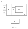
[0032] これより、本開示の実施形態に従った例示的な電子ビーム検査(EBI)システム10を示す図1Aを参照する。図1Aに示されているように、EBIシステム10は、主チャンバ11と、ロード/ロックチャンバ20と、電子ビームツール100と、機器フロントエンドモジュール(EFEM:equipment front end module)30と、を含む。電子ビームツール100は主チャンバ11内に配置されている。
[0032] Reference is now made to FIG. 1A, which illustrates an exemplary electron beam inspection (EBI)
[0033] EFEM30は、第1ローディングポート30a及び第2ローディングポート30bを含む。EFEM30は、1又は複数の追加のローディングポートも含み得る。第1ローディングポート30a及び第2ローディングポート30bは、例えば、検査対象のウェーハ(例えば、半導体ウェーハ、又は1もしくは複数の他の材料で作製されたウェーハ)又はサンプルを収容したウェーハFOUP(front opening unified pod)を受容することができる(本明細書ではウェーハ及びサンプルをまとめて「ウェーハ」と呼ぶことがある)。EFEM30内の1つ以上のロボットアーム(図示せず)が、ウェーハをロード/ロックチャンバ20へ移送することができる。
[0033] The
[0034] ロード/ロックチャンバ20はロード/ロック真空ポンプシステム(図示せず)に接続されており、このロード/ロック真空ポンプシステムは、ロード/ロックチャンバ20内のガス分子を除去して大気圧未満の第1の圧力を達成する。第1の圧力に達した後、1つ以上のロボットアーム(図示せず)が、ウェーハをロード/ロックチャンバ20から主チャンバ11へ移送することができる。主チャンバ11は主チャンバ真空ポンプシステム(図示せず)に接続されており、この主チャンバ真空ポンプシステムは、主チャンバ11内のガス分子を除去して第1の圧力未満の第2の圧力を達成する。第2の圧力に達した後、ウェーハは電子ビームツール100による検査を受ける。電子ビームツール100はシングルビームシステム又はマルチビームシステムとすることができる。電子ビームツール100にコントローラ19が電子的に接続されている。コントローラ19は図1Aにおいて、主チャンバ11、ロード/ロックチャンバ20、及びEFEM30を含む構造の外側に示されているが、コントローラ19がこの構造の一部である場合もあることは認められよう。
[0034] The load/
[0035] 本開示は主チャンバ11が電子ビーム検査ツールを収容している例を提供するが、最も広い意味での本開示の態様は、電子ビーム検査システムを収容しているチャンバに限定されないことに留意するべきである。本明細書で検討される原理を第2の圧力下で動作する他のツールにも適用できることは認められよう。
[0035] It should be noted that while the present disclosure provides an example in which the
[0036] 図1Bは、図1AのEBIシステムの一部であり得る例示的な電子ビームツール100Aを示す。電子ビームツール100A(本明細書では「装置100A」とも呼ぶ)は、電子源101と、銃アパーチャプレート(gun aperture plate)171と、コンデンサレンズ110と、ソース変換ユニット120と、一次投影システム130と、二次結像システム150と、電子検出デバイス140Mと、を備える。一次投影システム130は対物レンズ131を含み得る。表面7を有するサンプル1は、可動ステージ(図示せず)上に提供することができる。電子検出デバイス140Mは、複数の検出要素140_1、140_2、及び140_3を含み得る。一次投影システム130内にビームセパレータ160及び偏向スキャンユニット132を配置することができる。
[0036] FIG. 1B illustrates an exemplary
[0037] 電子源101、銃アパーチャプレート171、コンデンサレンズ110、ソース変換ユニット120、ビームセパレータ160、偏向スキャンユニット132、及び一次投影システム130は、装置100Aの一次光軸100_1と位置合わせすることができる。二次結像システム150及び電子検出デバイス140Mは、装置100Aの二次光軸150_1と位置合わせすることができる。
[0037] The
[0038] 電子源101は、カソード(図示せず)と、抽出器又はアノード(図示せず)と、を含み得る。動作中、電子源101はカソードから一次電子を放出するように構成され、一次電子は抽出器又はアノードによって抽出又は加速されて、一次ビームクロスオーバ(仮想(virtual)又は実)101sを形成する一次電子ビーム102を形成する。一次電子ビーム102は、一次ビームクロスオーバ101sから放出されているように可視化できる。
[0038] The
[0039] ソース変換ユニット120は、像形成要素アレイ(図1Bには示されていない)及びビーム制限アパーチャアレイ(図1Bには示されていない)を含むことができる。像形成要素アレイは複数の微小偏向器又は微小レンズを含むことができ、これらは、一次電子ビーム102の複数の一次ビームレット102_1、102_2、102_3に影響を与えると共に、一次ビームレット102_1、201_2、102_3の各々に一つずつ、一次ビームクロスオーバ101sの複数の平行な像(虚(virtual)又は実)を形成することができる。ビーム制限アパーチャアレイは、個々の一次ビームレット102_1、102_2、及び102_3の直径を制限するように構成できる。図1Bは一例として3つの一次ビームレット102_1、102_2、及び102_3を示すが、ソース変換ユニット120は任意の数の一次ビームレットを形成するように構成され得ることは認められよう。例えば、ソース変換ユニット120は、3×3アレイの一次ビームレットを形成するように構成できる。ソース変換ユニット120は更に、プローブスポット102_1S、102_2S、及び102_3Sの収差を補償するように構成された収差補償器アレイを含み得る。いくつかの実施形態において、収差補償器アレイは、プローブスポット102_1S、102_2S、及び102_3Sのフィールド曲率収差をそれぞれ補償するように構成された微小レンズを有するフィールド曲率補償器アレイを含み得る。いくつかの実施形態において、収差補償器アレイは、プローブスポット102_1S、102_2S、及び102_3Sの非点収差をそれぞれ補償するように構成された微小非点収差補正器(micro-stigmator)を有する非点収差補償器アレイを含み得る。いくつかの実施形態において、像形成要素アレイ、フィールド曲率補償器アレイ、及び非点収差補償器アレイはそれぞれ、微小偏向器、微小レンズ、及び微小非点収差補正器の多数の層を含み得る。多層アレイの例は、全体が本願に含まれる米国特許出願第62/567,134号で更に記載されている。
[0039] The
[0040] コンデンサレンズ110は、一次電子ビーム102を集束するように構成されている。コンデンサレンズ110は更に、コンデンサレンズ110の集束力を変動させることによって、ソース変換ユニット120の下流の一次ビームレット102_1、102_2、及び102_3の電流を調整するように構成できる。これにより、ビームレット102_1、102_2、及び102_3の集束状態をコンデンサレンズ110によって変化させることができる。あるいは、この電流の変化は、個々の一次ビームレットに対応するビーム制限アパーチャアレイ内のビーム制限アパーチャの半径方向のサイズを変更することによって実行できる。従って、ビームレットの電流は、ビームレット経路に沿った異なる位置では異なる可能性がある。ビームレット電流は、サンプル表面上のビームレットの電流(例えばプローブスポット電流)が所望の量に設定されるように調整すればよい。
[0040] The
[0041] コンデンサレンズ110は、第1主面の位置が可動であるように構成できる可動コンデンサレンズとしてもよい。可動コンデンサレンズは、磁気型、又は静電型、又は電磁型(例えば複合)であるように構成できる。可動コンデンサレンズは、米国特許第9,922,799号及び米国特許出願公報第2017/0025243号に更に記載されている。これらは双方とも全体が本願に含まれる。いくつかの実施形態において、コンデンサレンズは、ビームレットの電流を変動させながらオフアクシスビームレットの回転角を不変のままに維持できる回転防止レンズ(anti-rotation lens)としてもよい。いくつかの実施形態において、コンデンサレンズ110は、可動の第1主面を有する回転防止レンズを含む、可動回転防止コンデンサレンズとすることができる。回転防止又は可動回転防止コンデンサレンズは、参照により全体が本願に含まれる国際公報WO2018/122176号に更に記載されている。
[0041] The
[0042] 対物レンズ131は、図示されている実施形態に示すように、検査のためビームレット102_1、102_2、及び102_3をサンプル1上に集束させるように構成することができ、表面7上に3つのプローブスポット102_1S、102_2S、及び102_3Sを形成できる。銃アパーチャプレート171は、動作中、一次電子ビーム102の周辺電子を遮断してクーロン効果を低減するように構成されている。クーロン効果は、一次ビームレット102_1、102_2、102_3のプローブスポット102_1S、102_2S、及び102_3Sの各々のサイズを拡大させ、これによって検査分解能を劣化させる可能性がある。
[0042] The
[0043] ビームセパレータ160は、例えば、静電双極子場E1及び磁気双極子場B1を発生する静電偏向器を含むウィーンフィルタ(Wien filter)とすればよい。ビームセパレータ160は、ローレンツ力を用いて、通過する電子に影響を及ぼすことができる。ビームセパレータ160は、静電双極子場E1及び磁気双極子場B1を発生するように活性化できる。動作中、ビームセパレータ160は、一次ビームレット102_1、102_2、及び102_3の個々の電子に対し、静電双極子場E1によって静電力を加えるように構成できる。静電力は、個々の電子に対してビームセパレータ160の磁気双極子場B1によって加えられる磁力と大きさは等しいが方向は反対であり得る。一次ビームレット102_1、102_2、及び102_3は、実質的に真っすぐビームセパレータ160を通過し得る。
[0043] The
[0044] 偏向スキャンユニット132は、動作中、一次ビームレット102_1、102_2、及び102_3を偏向させて、プローブスポット102_1S、102_2S、及び102_3Sを表面7のセクション内の個々のスキャンエリアでスキャンするように構成されている。一次ビームレット102_1、102_2、及び102_3によってプローブスポット102_1S、102_2S、及び102_3Sでサンプル1が照明されることに応答して、二次電子がサンプル1から放出され、動作中にサンプル1から放出される3つの二次電子ビーム102_1se、102_2se、及び102_3seを形成する。二次電子ビーム102_1se、102_2se、及び102_3seの各々は典型的に、二次電子(例えば、≦50eVの電子エネルギを有する)及び後方散乱電子(例えば、50eVと一次ビームレット102_1、102_2、及び102_3の入射エネルギとの間の電子エネルギを有する)を含む様々なエネルギを有する電子を含む。
[0044] The
[0045] ビームセパレータ160は、二次電子ビーム102_1se、102_2se、及び102_3seを二次結像システム150の方へ偏向させるように構成されている。二次結像システム150はこの後、二次電子ビーム102_1se、102_2se、及び102_3seを電子検出デバイス140Mの検出要素140_1、140_2、及び140_3上に集束させる。検出要素140_1、140_2、及び140_3は、対応する二次電子ビーム102_1se、102_2se、及び102_3seを検出し、対応する信号を発生するように配置されている。これらの信号は、例えばサンプル1の対応するスキャンエリアの像を構築するため、信号処理ユニット(図示せず)に送信され得る。
[0045] The
[0046] ビームセパレータ160は、二次電子ビームを二次結像システム150の方へ角度αだけ偏向させるように構成できる。角度αは、一次光軸100_1と二次光軸150_1との角度として規定され得る。角度αは、光軸上の一次電子ビームレットとこれに対応する二次電子ビームレットとの分離角を表し得る。いくつかの実施形態において、角度αは5~25度の範囲内に設定できる。
[0046] The
[0047] 上記で検討したように、ビームセパレータ160は、ウィーンフィルタ等の磁気偏向器を含む偏向デバイスとすればよい。偏向デバイスは、通過する電子を偏向することができる。電子の偏向方向と偏向角は、電子の移動方向とエネルギ(例えば速度によって表すことができる)に依存し得る。一次電子はサンプル1の方へ進み、二次電子はサンプル1の表面7から発生してサンプル1から離れる方へ進み得る。このため、二次電子又は後方散乱電子とは異なる方向に移動する一次電子を、二次電子又は後方散乱電子から区別することができる。従って、一次ビームレット102_1、102_2、及び102_3は実質的に真っすぐビームセパレータ160を通過することができ、二次電子ビーム102_1se、102_2se、及び102_3seは、例えば角度αだけ光軸100_1から離れる方へ偏向する。
[0047] As discussed above, the
[0048] しかしながら、一次ビームレット102_1、102_2、及び102_3自体が異なるエネルギレベルの電子を含むことがある。従って、一次ビームレット102_1、102_2、及び102_3の各々で分散が発生する可能性がある。分散は、一次ビームレット102_1、102_2、及び102_3に影響を及ぼして、所望の形状から逸脱するか又は広がったプローブスポットをサンプル1上に形成し得る。その結果として、分散により、プローブスポットは例えば楕円形状に形成されるか又は拡大することがある。ビームセパレータ160により生じた分散は結像解像度を低下させる恐れがある。
[0048] However, the primary beamlets 102_1, 102_2, and 102_3 themselves may contain electrons of different energy levels. Thus, dispersion may occur in each of the primary beamlets 102_1, 102_2, and 102_3. The dispersion may affect the primary beamlets 102_1, 102_2, and 102_3 to form a probe spot on the
[0049] 更に、分散は二次電子ビーム102_1se、102_2se、及び102_3seに影響を及ぼして、電子検出デバイス140M上により大きいスポットを形成する可能性がある。分散は二次電子収集効率を低下させ、クロストークの一因となる恐れがある。
[0049] Additionally, dispersion can affect secondary electron beams 102_1se, 102_2se, and 102_3se to form larger spots on
[0050] 図1Bにおいて、一次投影システム130内のビームレットの経路は単なる概略であり得る。例えば図1Bに示されているように、ビーム偏向器160、偏向スキャンユニット132、及び対物レンズ131を通って直線的に進むビームレットの点線の表現は、一次投影システム130のような電子光学要素又はシステムへ入射しこれらから出射するビームレット間の対応関係を示し得る。すなわち、ビームレットの軌道は図1Bの一次投影システム130内に示されたものとは異なることがある。ビームレットの相対位置は電子光学要素の構成及び動作モードによって変化し得る。
[0050] In FIG. 1B, the paths of the beamlets in the
[0051] 分離角αは様々な基準に基づいて設定することができる。いくつかの実施形態において、分離角αは分散の影響を最小限に抑えるように設定され得る。例えば、分離角αはできる限り小さく選択することができる。ビームセパレータ160は、ビームセパレータ160によって発生する静電双極子場E1及び磁気双極子場B1の大きさが最小限に抑えられるように、二次ビームレットをできる限り少量だけ偏向するように構成できる。分散の影響を最小限に抑えるためには、E1及びB1の大きさを低減することが効果的であり得る。
[0051] The separation angle α can be set based on various criteria. In some embodiments, the separation angle α can be set to minimize the effects of dispersion. For example, the separation angle α can be selected to be as small as possible. The
[0052] しかしながら、分離角αを小さくすると、一次光軸100_1と二次光軸150_1との間の利用可能な空間が制限され得る。空間の制限は、二次結像システム150に実装上の制約を加える。このような制約は、レンズのような二次結像システム150内の要素のサイズ及び位置の柔軟性を制限する可能性がある。
[0052] However, reducing the separation angle α may limit the available space between the primary optical axis 100_1 and the secondary optical axis 150_1. Space limitations impose packaging constraints on the
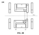
[0053] 図1Cは、装置100Aの一部を形成し得る検出システム100A-Dの例示的な構成を示す。検出システム100A-Dは、二次結像システム150及び電子検出デバイス140Mを含み得る。二次結像システム150は、ズームレンズ151と、投影レンズ152と、スキャン防止偏向ユニット157と、を含むことができ、これらは全て二次光軸150_1と位置合わせされ得る。電子検出デバイス140の検出要素140_1、140_2、及び140_3は、検出面SP3上に配置することができる。ズームレンズ151、投影レンズ152、及び対物レンズ131は共に、サンプル表面7の像を検出面SP3上に投影することができる。これらの要素は、偏向スキャンユニット132がオフである場合、二次電子ビーム102_1se、102_2se、及び102_3seを集束して、それぞれ検出要素140_1、140_2、及び140_3上に二次電子スポットを形成できる。スキャン防止偏向ユニット157は、偏向スキャンユニット132がビームレット102_1、102_2、及び102_3を各領域でスキャンする場合、二次電子スポットを対応する検出要素内に保持するように構成できる。
1C shows an exemplary configuration of
[0054] サンプル1の表面7から検出面SP3までの合計結像倍率は、検出要素上のプローブスポットのピッチ(例えば、検出要素140_1、140_2、及び140_3上の二次電子スポット間のピッチ)及びサンプル1上のプローブスポットのピッチ(例えば、プローブスポット102_1S、102_2S、及び102_3S間のピッチ)に基づいて決定することができる。
[0054] The total imaging magnification from
[0055] サンプル表面7の各プローブスポットを1つの検出要素上に結像することにより、複数のプローブスポットと複数の検出要素との間の対応関係を保証できる。いくつかの実施形態において、サンプル1上のプローブスポットピッチは異なる検査用途では異なる可能性があり、これに応じて倍率も変化し得る。
[0055] By imaging each probe spot on the
[0056] ズームレンズ151は、2つのレンズ151_11及び151_12を含み得る。レンズ151_11及び151_12は静電レンズとすることができる。ズームレンズ151の像面は伝達面(transfer plane)SP2にあるように構成できる。伝達面SP2にフィールドレンズを提供することができる。いくつかの実施形態において、伝達面SP2の位置は、低速二次電子検出モード及び後方散乱電子検出モードのような異なるモードでは異なる可能性がある。 [0056] The zoom lens 151 may include two lenses 151_11 and 151_12. The lenses 151_11 and 151_12 may be electrostatic lenses. The image plane of the zoom lens 151 may be configured to be at a transfer plane SP2. A field lens may be provided at the transfer plane SP2. In some embodiments, the location of the transfer plane SP2 may be different for different modes, such as a low-energy secondary electron detection mode and a backscattered electron detection mode.
[0057] 投影レンズ152は、静電レンズ152_11及び磁気レンズ152_12を含み得る。投影レンズ152の像面は検出面SP3にあるように構成できる。サンプル表面7から伝達面SP2への第1の結像倍率レベルは、対物レンズ131及びズームレンズ151によって実現できる。伝達面SP2から検出面SP3への第2の結像倍率レベルは、投影レンズ152によって実現できる。サンプル表面7から検出面SP3までの合計結像倍率は、第1の結像倍率レベルと第2の結像倍率レベルとの積に等しいものであり得る。いくつかの実施形態において、第2の結像倍率レベルは第1の結像倍率レベルよりも大きいように構成できる。第2のレベルを第1のレベルよりも大きく設定することは、低速二次電子検出モード等のいくつかの結像モードでは有利であり得る。
[0057] The projection lens 152 may include an electrostatic lens 152_11 and a magnetic lens 152_12. The image plane of the projection lens 152 may be configured to be at the detection plane SP3. A first imaging magnification level from the
[0058] ズームレンズ151はズーム機能を実行することができる。レンズ151_11及び151_12の集束力を調整することにより、第1の結像倍率レベルを変動させて合計結像倍率の所望の値を達成することができる。投影レンズ152は回転防止機能を実行することができる。磁気レンズ152_12の磁場及び静電レンズ152_11の集束力を調整することにより、検出面SP3における合計像回転及び第2の結像倍率レベルが一定の状態を維持するように設定できる。スキャン防止偏向ユニット157はスキャン防止機能を実行することができる。偏向スキャンユニット132を用いて二次電子ビームを同期的に偏向させることにより、検出面SP3上の二次電子スポットの変位を実質的に打ち消すことができる。その結果として、複数のプローブスポットと複数の検出要素との間の対応関係を維持できる。
[0058] The zoom lens 151 can perform a zoom function. By adjusting the focusing power of the lenses 151_11 and 151_12, the first imaging magnification level can be varied to achieve a desired value of the total imaging magnification. The projection lens 152 can perform an anti-rotation function. By adjusting the magnetic field of the magnetic lens 152_12 and the focusing power of the electrostatic lens 152_11, the total image rotation and the second imaging magnification level at the detection plane SP3 can be set to remain constant. The anti-scan deflection unit 157 can perform an anti-scan function. By synchronously deflecting the secondary electron beam using the
[0059] 検出システム100A-Dの例示的な動作は以下を含み得る。例えば、対物レンズ131は、プローブスポット102_1S、102_2S、及び102_3Sからそれぞれ発生した二次電子ビーム102_1se、102_2se、及び102_3seを集束し、像面SP1_se上に3つのプローブスポットの第1の二次電子像を形成することができる。像面SP1_seはズームレンズ151の下方にあり、対物レンズ131の動作条件の変化と共に移動し得る。ビームセパレータ160は、二次電子ビーム102_1se、102_2se、及び102_3seが二次光軸150_1に沿って二次結像システム150に入射するように、これらのビームを偏向させることができる。次いで、ズームレンズ151は二次電子ビーム102_1se、102_2se、及び102_3seを集束し、伝達面SP2上に3つのプローブスポットの第2の二次電子像を形成することができる。次いで、投影レンズ152は二次電子ビーム102_1se、102_2se、及び102_3seを集束して、検出面SP3上に3つのプローブスポットの第3の二次電子像を形成することができる。
[0059] Exemplary operations of the
[0060] 第1のズームレンズ151_11及び第2のズームレンズ151_12を含むズームレンズ151は、対物レンズ131の結像条件及び一次電子ビームの複数のビームレットが変化する場合に、サンプル1と検出面SP3との間の所望の結像倍率を達成するように調整することができる。例えば、第1のズームレンズ151_11及び第2のズームレンズ151_12は、二次電子ビーム102_1se、102_2se、及び102_3seのピッチが検出要素140_1、140_2、及び140_3のピッチと一致するように調整できる。磁気レンズ152_12及び静電レンズ152_11を含む投影レンズ152は、結像条件が変化した場合に、二次電子ビーム102_1se、102_2se、及び102_3seの向きが検出要素140_1、140_2、及び140_3の向きと一致するように調整できる。スキャン防止偏向ユニット157は、偏向スキャンユニット132がサンプル1上の各領域でビームレット102_1、102_2、及び102_3をスキャンする動作中に、二次電子ビーム102_1se、102_2se、及び102_3seを検出要素140_1、140_2、及び140_3内に保持するように動作させることができる。
[0060] The zoom lens 151, including the first zoom lens 151_11 and the second zoom lens 151_12, can be adjusted to achieve a desired imaging magnification between the
[0061] 上記で検討したように、ビームセパレータ160は、例えば分散の影響を最小限に抑えるため、二次ビームレットを小さい角度αだけ偏向させるように構成できる。角度αは例えば5~25度内に設定すればよい。分離角αが小さい場合、二次結像システム150及び一次投影システム130のための空間が制限され得る。ズームレンズ151の第1のレンズ151_11のようなビームセパレータ160に最も近い要素は、このような空間の制約によって最も大きい影響を受ける可能性がある。また、これら2つのシステムが、例えばより多くのビームレット及び検出要素を用いることで更に複雑になるにつれて、空間の制約はいっそう厳しくなり得る。2つのシステム内のレンズを小型化することは可能であるが、結像品質が劣化する恐れがある。例えば、レンズの内径が大きくなればなるほど、レンズによって発生する収差は小さくなる。それと同時に、レンズの配置がビームセパレータ160の近くになればなるほど、レンズによって発生する収差は小さくなる。二次結像システム150内で発生する収差は二次電子収集効率を低下させると共にクロストークの一因となり得るので、収差を最小限に抑えることが望ましい。しかしながら、実装上の制約があるので、内径の大きいレンズをビームセパレータ160の近くに配置することは難しい。従って、二次結像システム150で発生する収差を最小限に抑える観点からは、より大きい空間をレンズの収容のため利用できるように分離角αをできる限り大きく設定することが望ましい。このように、ビームセパレータ160からの分散の影響を最小限に抑えることと二次結像システム150からの収差を最小限に抑えることとの間には、トレードオフの関係が存在する。その結果として、分離角αは、一次電子像解像度と二次電子検出効率及びクロストークの要件のバランスを取るように選択され得る。静電レンズは通常、同等の磁気レンズよりも占有する空間が小さいが、磁気レンズよりも発生する収差が大きい。従って、いくつかの実施形態では、図1Cのズームレンズ151のレンズ151_11のような二次結像システム内のズームレンズの第1のレンズとして、電磁複合レンズが提供される。電磁複合レンズは、コイルを備える従来の磁気レンズよりもコンパクトにすることができるので、小さい分離角αが設定される場合に小さい収差を有する第1のレンズを使用し、これによって、分散の影響と収差が双方とも抑えられた検査ツールを達成する柔軟性の増大が可能となる。
[0061] As discussed above, the
[0062] 例えば二次結像システム150内の空間制限という理由から、通常、ズームレンズのレンズは静電レンズとすることができる。一例として、静電レンズは2つの端部電極及び1つ以上の内部電極を含み、アインツェルレンズ(Einzel lens)として機能し得る。アインツェルレンズでは、ビーム入射側とビーム出射側の端部電極は等しい電位に設定され、1つ以上の内部電極は、端部電極に対して正(すなわちポジティブモード)に、負(すなわちネガティブモード)に、又は、負及び正(すなわち2つ以上の内部電極を使用し得る組み合わせモード)に、バイアスされ得る。二次結像システム150が接地電位で動作することを保証するため、アインツェルレンズの端部電極は接地電位に設定することができる。
[0062] For reasons of space limitations within the
[0063] 一般に、磁気レンズは静電レンズよりも小さい収差を発生し得る。しかしながら、調整可能な集束力を有する従来の磁気レンズはコイル巻線を含むので、かさばる。従来の磁気レンズは、実装上の制約がある状況では理想的でない可能性がある。従って二次結像システム150は、例えばズームレンズ151においてアインツェルレンズを使用できる。
[0063] In general, magnetic lenses can produce smaller aberrations than electrostatic lenses. However, conventional magnetic lenses with adjustable focusing power include coil windings and are bulky. Conventional magnetic lenses may not be ideal in situations with packaging constraints. Thus,
[0064] アインツェルレンズは、二次結像システム150において、ポジティブモード、ネガティブモード、又は組み合わせモードで動作させることができる。ポジティブモードにおける絶対電圧は他のモードよりも高い。収差の効果を低減するには高い電圧を用いることが有利であり得るが、そうするとアーク放電のリスクを招く恐れがある。例えば二次結像システム150において、実装上の制約があるので導電性電極を相互に近接して配置した場合、多くのアーク放電経路が存在し得るので、電気的な安全のためには高電圧を回避しなければならない。従って、アインツェルレンズをネガティブモードで動作させることが望ましい場合がある。
[0064] The Einzel lens can be operated in the
[0065] 本開示のいくつかの実施形態では、ズームレンズ内の1つのレンズを、磁気レンズと静電レンズを含む電磁複合レンズとすることができる。複合レンズの磁気レンズは永久磁石を含み得る。複合レンズの磁気レンズは複合レンズの合計集束力の一部を提供することができ、静電レンズは合計集束力の残り部分を構成する。複合レンズの静電レンズは、純粋なアインツェルレンズよりも低い電圧を用いるポジティブモードで動作させることができる。いくつかの実施形態によれば、電磁複合レンズを用いたズームレンズの収差は、全てのレンズが静電型である典型的なズームレンズに比べて低減できる。 [0065] In some embodiments of the present disclosure, one lens in a zoom lens can be an electromagnetic compound lens that includes a magnetic lens and an electrostatic lens. The magnetic lens of the compound lens can include a permanent magnet. The magnetic lens of the compound lens can provide a portion of the total focusing power of the compound lens, and the electrostatic lens constitutes the remaining portion of the total focusing power. The electrostatic lens of the compound lens can be operated in a positive mode that uses a lower voltage than a pure Einzel lens. According to some embodiments, aberrations of a zoom lens using an electromagnetic compound lens can be reduced compared to a typical zoom lens in which all lenses are electrostatic.
[0066] これより、本開示の実施形態に従った電磁複合レンズ210Aの例示的な構成を示す図2Aを参照する。図2Aの複合レンズは二次結像システム150の一部を形成し得る。例えば複合レンズ210Aは、図1Cの二次結像システム150のズームレンズ151の第1のレンズ151_11として提供することができる。このため、複合レンズ210Aはビームセパレータ160と投影レンズ152との間に配置され得る。複合レンズ210Aは、軸210_1と位置合わせすることができる。例えば複合レンズ210Aが第1のレンズ151_11として提供される場合のように、いくつかの実施形態では、軸210_1は軸150_1とすることができる。複合レンズ210Aは軸210_1を中心として回転対称であり得る。
[0066] Reference is now made to FIG. 2A, which illustrates an exemplary configuration of an
[0067] 複合レンズ210Aは、永久磁石211と、第1の磁極片212と、第2の磁極片213と、第1の電極215と、第2の電極216と、を含み得る。磁石211は、軸210_1の周りに、軸210_1に沿った第1の磁極片212と第2の磁極片213との間に提供することができる。第1及び第2の磁極片212、213は、軸210_1に沿って第1の電極215と第2の電極216との間に提供することができる。コンポーネント211、212、213、215、及び216は、環状の形状を有し得る。コイルに比べて永久磁石は占有する空間が小さく、発生する熱が小さい可能性があり、ドライバに対する接続を必要としない。従って、永久磁石は高電圧環境での配置に適切であり得る。
[0067] The
[0068] 磁石211は、軸210_1に平行とすることができる長手方向に磁化方向を有し得る。第1の磁極片212及び第2の磁極片213は、導電性の磁性材料によって形成することができる。いくつかの実施形態において、第1及び第2の磁極片212及び213のうち一方又は双方は磁石211と直接に接触し得る。磁石211、第1の磁極片212、及び第2の磁極片213によって、磁気回路が形成され得る。磁極片212及び213は、磁石211によって発生した磁場を整形し方向付けるように提供できる。磁極片212及び213は、相互に物理的に接触しないように別個に提供できる。
[0068] The
[0069] 第1及び第2の磁極片212、213は非磁性ギャップG1を形成することができる。磁石211によって発生した磁場を軸210_1の方へ向かわせるように、ギャップG1は磁石211の半径方向内側に形成され得る。ギャップG1は、軸210_1の周りの環状領域に延出する(sweep out)ことができる。ギャップG1によって形成された延出環状領域は、磁石211の内径よりも小さい外径を有し得る。ギャップG1は自由空間とするか、又は、磁場に対してほとんどもしくは全く効果を持たない、すなわち透磁率が1に近いかもしくは1である材料を部分的にもしくは全体的に充填することができる。
[0069] The first and
[0070] 複合レンズ210Aは、磁石211、第1の磁極片212、及び第2の磁極片213によって形成することができる磁気レンズを含む。磁気レンズの励起は磁石211によって与えられる。ギャップG1を通って磁場210-mfが出現し得る。図2Aは磁場210-mfの磁力線を示している。磁場は、第1及び第2の磁極片212、213間のギャップG1を通って軸210_1の周りのエリアへ漏れる可能性がある。このため、複合レンズ210A内を進んでいる電子は磁気レンズの磁場によって影響を受け得る。第1及び第2の磁極片212、213のうち一方又は双方が磁石211から離隔している場合、第1及び第2の磁極片212、213は、磁石211から離隔した部分の方がギャップG1よりも強い磁気結合を有し得る。従って、磁場はギャップG1を通って優先的に漏れる可能性がある。いくつかの実施形態において、第1及び第2の磁極片212、213は異なる直径を有し得る。例えば、第1の磁極片212は第2の磁極片213とは異なる内径を有し得る。
[0070] The
[0071] 複合レンズ210Aは、第1及び第2の磁極片212、213、第1の電極215、並びに第2の電極216によって形成することができる静電レンズを含む。第1及び第2の電極215、216は端部電極を形成し得る。第1及び第2の電極215、216は導電性材料によって形成できる。コンポーネント212、213、215、及び216に電圧を印加することができる。コンポーネント212、213、215、及び216のうち2つが異なる電位に設定されている場合、静電場を発生させることができる。例えば図2Aにおいて、第1の電極215は第1の磁極片212とは異なる電位に設定され得る。このため、それらの間に電場を形成することができる。同様に、第2の電極216は第2の磁極片213とは異なる電位に設定され得る。第1及び第2の磁極片212、213の電位は同一とすることができる。第1及び第2の電極215、216の電位も、(アインツェルレンズにおけるように)同一とすることができる。図2Aは電場210-efの等電位線を示している。複合レンズ210Aは、例えばギャップG1の領域で横断面交差軸210_1を中心として対称であるように構成できる。
[0071] The
[0072] いくつかの実施形態において、第1の磁極片212及び第2の磁極片213は相互に電気的に接続され得る。このため、第1の磁極片212及び第2の磁極片213は単一の電極を形成することができ、第1の磁極片212及び第2の磁極片213に単一の電圧を印加することができる。
[0072] In some embodiments, the
[0073] 複合レンズ210Aの集束力は調整可能とすることができる。例えば、コンポーネント212、213、215、及び216で構成された静電レンズの電場は、静電レンズの電極の電圧を変動させることによって調整できる。磁石211は永久磁石であり、その磁化は固定され得るので、磁気レンズで発生した磁場は固定されたまま維持し得る。複合レンズの集束力は、磁場と電場の双方に依存し得る。このため、磁場が固定されている場合、集束力の調整機能は複合レンズの静電部分によって提供できる。
[0073] The focusing power of
[0074] 複合レンズ210Aは静電レンズと磁気レンズを含むことができ、静電レンズによって調整可能とすることができる。静電レンズの調整は、第1の電極215、第2の電極216、及び、第1の磁極片212又は第2の磁極片213を含み得る中央電極に印加される電圧を調整することによって実行できる。
[0074] The
[0075] 図2Bは、本開示の実施形態に従った複合レンズ210Bの別の例示的な構成を示す。複合レンズ210Bは、図2Aに関して上記で検討した複合レンズ210Aと同様であり得るが、以下の例示的な相違点がある。複合レンズ210Bは、それぞれ軸210_1に沿った方向に、磁石211と第1の磁極片212との間のギャップGaと、磁石211と第2の磁極片213との間のギャップGbと、を含み得る。第1及び第2の磁極片212、213は、ギャップG1よりもギャップGa及びGbにおいて強い磁気結合を有し得る。第1及び第2の磁極片212、213は異なる形状を有し得る。第1の磁極片212は第2の磁極片213よりも小さい内径を有し得る。更に、複合レンズ210Bは、ギャップG1内に配置された電極214も含み得る。
[0075] FIG. 2B illustrates another exemplary configuration of a
[0076] 第1及び第2の磁極片212、213は、軸210_1に沿った様々な位置にギャップG1が形成されるような形状とすることができる。図2Bに示されているように、ギャップG1は軸方向における磁石211の一端に形成され得る。ギャップG1は磁石211の一端の近くに形成され得る。例えばギャップG1は、軸210_1の方向における磁石211の反対側の端部よりも磁石211の一端の近くにあり得る。ギャップG1は、電子ビームの電子の入射側にあるように位置決めされ得る。例えば、図2Bに示された図で右側端部から二次ビームの二次電子が入射するように、複合レンズ210Bを二次結像システム内に配置することができる。軸210_1は二次光軸150_1(図1Cを参照のこと)と同一線上にあり得る。電子は、第1の磁極片212の開口を通って複合レンズ210Bに入射することができる。このため、電子は、複合レンズ210Bに入射した直後にギャップG1から出現する磁場によって影響を受ける可能性がある。電子が入射する複合レンズ210Bの端部の近くにギャップG1を位置決めすると、早期に磁場が電子に影響を及ぼすことを保証すると共に、複合レンズ201Bの収差を低減することができる。
[0076] The first and
[0077] 電極214は、ギャップG1を部分的に又は全体的に覆うように提供できる。いくつかの実施形態において、電極214は完全にギャップG1内に提供され、ギャップG1の外部には延出しない。電極214は非磁性材料によって形成することができる。電極214は、磁石211により発生した磁場と干渉しないように、磁場に対してほとんど又は全く効果を持たない材料で形成することができる。磁石211の帯電を回避するため、電極214は完全にギャップG1を塞ぐことができる。従って、例えば軸210_1に沿って複合レンズ210B内を進んでいる電子が磁石211に衝突することを防止できる。これにより、電荷が磁石211上に蓄積することが防止されるので、複合レンズ210Bの静電レンズの静電特性が電荷によって変化するのを防ぎ、結果として静電レンズの集束力を安定して保つことが可能となる。更に、コンポーネント211、212、213のジオメトリは、電子が磁石211に到達する可能性を低下させるように構成できる。例えば、磁石211の環形状の厚さは第1及び第2の磁極片212、213よりも小さくすることができる。いくつかの実施形態において、磁石211の内径は第1及び第2の磁極片212、213よりも大きくすることができる。磁石211の内径は第1及び第2の磁極片212、213よりも著しく大きくてもよい。ギャップG1は、磁石211と第1の磁極片212との半径方向のサイズの差よりも小さく(半径方向は軸210_1に対して垂直である)、又は、磁石211と第2の磁極片213との半径方向のサイズの差よりも小さくすることができる。このような構成では、複合レンズ210B内を進んでいる電子が磁石211に到達する可能性を低下させることができる。
[0077] The
[0078] 複合レンズ210Bは静電レンズ及び磁気レンズを含むことができる。複合レンズ210Bの磁気レンズは、コンポーネント211、212、213によって形成できる。コンポーネント211、212、213によって発生した磁場は、ギャップG1を通って漏れて、軸210_1に沿って進む電子に影響を及ぼす可能性がある。複合レンズ210Bの静電レンズは、コンポーネント212、213、214、215、及び216によって形成できる。第1の電極215及び第2の電極216と共に、第3の電極を複合レンズ210Bの静電レンズに提供することができる。第3の電極は電極214を含み得る。電極214は、第1及び第2の磁極片212、213のうち一方又は双方と直接に接触し得る。いくつかの実施形態において、複合レンズ210Bの静電レンズ及び磁気レンズは共通のコンポーネントを用いて形成することができる。例えば、第1の磁極片212及び第2の磁極片213は、複合レンズ210Bの静電レンズと複合レンズ210Bの磁気レンズの双方の構成コンポーネントであり得る。他の実施形態では、例えば後で検討されるように、静電レンズ及び磁気レンズのコンポーネントは相互に排他的であり得る。
[0078] The
[0079] いくつかの実施形態において、電極214は、第1の磁極片212又は第2の磁極片213と同一又は異なる内径を有し得る。例えば図2Bに示されているように、電極214は、第1の磁極片212の内径D2よりも大きい内径D1を有する。更に、電極214は、第1の磁極片212と電極214との間、又は第2の磁極片213と電極214との間にギャップが形成されるように配置され得る。
[0079] In some embodiments, the
[0080] 図2Cは、本開示の実施形態に従った複合レンズ210Cの別の例示的な構成を示す。複合レンズ210Cは、上記で検討した複合レンズ210A及び複合レンズ210Bと同様であり得るが、以下の例示的な相違点がある。複合レンズ210Cは、ギャップG1の内側に配置された電極214を含み得る。複合レンズ210Cは、それぞれ軸210_1に沿った方向に、電極214と第1の磁極片212との間のギャップGcと、電極214と第2の磁極片213との間のギャップGdと、を含み得る。電極214は、第1及び第2の磁極片212、213の各々よりも大きい内径を有し得る。複合レンズ210Cは、電子が磁石211に衝突する可能性が低いように構成できる。
[0080] FIG. 2C illustrates another exemplary configuration of a
[0081] これより、本開示の実施形態に従った複合レンズ220Aの例示的な構成を示す図3Aを参照する。複合レンズ220Aは、第1及び第2の磁極片212、213を覆う電極214を含み得る。電極214は、軸210_1に面した第1及び第2の磁極片212、213の内面を覆うことができる。電極214は、軸210_1に沿って第1の磁極片212の端部から第2の磁極片213の端部まで延出し得る。電極214は、軸210_1に面した第1及び第2の磁極片212、213の内面の実質的に全てを覆うことができる。
[0081] Reference is now made to FIG. 3A, which illustrates an exemplary configuration of a
[0082] 複合レンズ220Aにおいて、第1の磁極片212及び第2の磁極片213は、磁気的に伝導性かつ非導電性の材料によって形成することができる。第1及び第2の磁極片212、213のうち一方又は双方の材料は電気絶縁体であり得る。電極214は非磁性材料によって形成することができる。
[0082] In the
[0083] 複合レンズ220Aは静電レンズ及び磁気レンズを含むことができる。複合レンズ220Aの磁気レンズは、コンポーネント211、212、213によって形成できる。コンポーネント211、212、213によって発生した磁場は、ギャップG1を通って漏れて、軸210_1に沿って進む電子に影響を及ぼす可能性がある。複合レンズ220Aの静電レンズは、コンポーネント214、215、及び216によって形成できる。電極214は、第1及び第2の磁極片212、213のうち一方又は双方と直接に接触し得る。いくつかの実施形態では、電極214と第1及び第2の磁極片212、213との間にギャップを設けてもよい。例えば、電極214は第1及び第2の磁極片212、213から半径方向に離隔し得る。コンポーネント214、215、及び216のうち2つのコンポーネントを異なる電位に設定することにより、複合レンズ220Aにおいて電場を発生させることができる。
[0083] The
[0084] 複合レンズ220Aは、設計の柔軟性の向上を可能とすることができる。例えば、電極214、第1の電極215、及び第2の電極216等の電気伝導性を有するコンポーネントにより、電場を発生させることができる。第1及び第2の磁極片212、213は、静電レンズを形成するため導電性材料で形成する必要はないので、複合レンズ220Aを構築する材料の選択において柔軟性を増すことができる。
[0084]
[0085] 図3Bは、本開示の実施形態に従った複合レンズ220Bの別の例示的な構成を示す。複合レンズ220Bは、図3Aに関して上記で検討した複合レンズ220Aと同様であり得るが、以下の例示的な相違点がある。複合レンズ220Bは、第1の磁極片212、第2の磁極片213、及び磁石211を実質的に覆う形状を有する電極214を含み得る。電極214は、第1の磁極片212、第2の磁極片213、及び磁石211を取り囲むことができる。電極214は、実質的にU字形のリングを含む形状を有し得る。例えば電極214は、軸210_1を中心とした回転対称のU字形断面を含み得る。電極214は、長手方向すなわち軸210_1に沿って第1及び第2の磁極片212、213を覆う部分と、半径方向に第1及び第2の磁極片212、213を覆う部分と、を含み得る。電極214は、軸210_1に面した第1及び第2の磁極片212、213の内面を覆うことができる。電極214は、軸210_1に沿って第1の磁極片212の端部から第2の磁極片213の端部まで延出し得る。電極214は、第1及び第2の磁極片212、213の端面も覆うことができる。電極214は、第1の磁極片212、第2の磁極片213、及び磁石211の外周の3つの側を覆うことができる。例えば電極214は、コンポーネント211、212、及び213のグループの軸方向内側と半径方向端部側を覆うことができる。いくつかの実施形態において、電極214は、第1の磁極片212、第2の磁極片213、及び磁石211の外周の別の側、例えば軸方向外側を覆うことも可能である。電極214は、第1の磁極片212、第2の磁極片213、及び磁石211を完全に取り囲み得る。
[0085] Figure 3B illustrates another exemplary configuration of a
[0086] いくつかの実施形態では、電極214は、電極214と電極214が覆っているコンポーネントとの間にギャップを設けることができる。電極214は、第1及び第2の磁極片212、213のうち一方又は双方と直接に接触し得る。例えば電極214は、軸210_1に沿った方向に第1の磁極片212からギャップGeだけ離隔すると共に、第2の磁極片213に接触することができる。
[0086] In some embodiments, the
[0087] いくつかの実施形態において、複合レンズはズームレンズ内のレンズとして使用することができる。ズームレンズは、これを通って進む電子を適切に制御できるように調整可能な集束力を有し得る。例えば、ズームレンズを用いて複数の検出要素間のクロストークを低減することができる。そのような場合、ズームレンズは、二次電子ビームのスポットが重複すること、又は、検出デバイスの隣接した検出要素に入射すること、を防止するように構成できる。ズームレンズは、各二次電子ビームのスポットサイズを、対応する電子検出要素よりも小さくするように構成できる。更にズームレンズは、対物レンズ131における集束の影響の変動を補償するように構成できる。複合レンズ210A、210B、210C、220A、及び220B等のレンズは、様々な結像条件を満たすため調整可能静電レンズによって調整できるように構成され得る。
[0087] In some embodiments, the compound lens can be used as a lens in a zoom lens. The zoom lens can have an adjustable focusing power so that the electrons traveling therethrough can be appropriately controlled. For example, a zoom lens can be used to reduce crosstalk between multiple detector elements. In such a case, the zoom lens can be configured to prevent the spots of the secondary electron beams from overlapping or impinging on adjacent detector elements of the detection device. The zoom lens can be configured to make the spot size of each secondary electron beam smaller than the corresponding electron detector element. Additionally, the zoom lens can be configured to compensate for variations in focusing effects in the
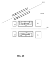
[0088] これより、本開示の実施形態に従った、電子ビームツールの二次結像システムにおける第1のレンズ151-11Aの例示的な構成を示す図4Aを参照する。第1のレンズ151-11Aは、図2Aから図2C及び図3Aから図3Bを参照して上記で検討したような電磁複合レンズを含み得る。第1のレンズ151-11Aは、図1Cを参照して上記で検討した二次結像システム150のズームレンズ151の一部として適用され得る。第1のレンズ151-11Aは、一次光軸100_1から離れる方へ偏向されて二次光軸150_1に沿って進む二次電子ビーム102_1se、102_2se、及び102_3seを集束するように構成できる。
[0088] Reference is now made to FIG. 4A, which illustrates an exemplary configuration of a first lens 151-11A in a secondary imaging system of an electron beam tool, according to an embodiment of the present disclosure. The first lens 151-11A may include an electromagnetic compound lens as discussed above with reference to FIGS. 2A-2C and 3A-3B. The first lens 151-11A may be applied as part of the zoom lens 151 of the
[0089] 図4Aに示されているように、第1のレンズ151-11Aは、永久磁石211、第1の磁極片212、第2の磁極片213、電極214、第1の端部遮蔽電極217、及び第2の端部遮蔽電極218を含む。コンポーネント211、212、213、214、217、及び218は、二次光軸150_1と位置合わせすることができる。第1の端部遮蔽電極217は、磁石211を外側から覆って磁石211を磁気的に遮蔽する部分217aを含み得る。このため、磁石211によって発生した磁場を一次光軸100_1へ漏れないようにすることができる。
[0089] As shown in FIG. 4A, the first lens 151-11A includes a
[0090] 第1及び第2の磁極片212、213は導電性の磁性材料によって形成することができる。いくつかの実施形態において、第1及び第2の磁極片212、213は電気絶縁体としてもよい。電極214は、導電性の非磁性材料によって形成することができる。第1及び第2の端部遮蔽電極217、218は、導電性かつ磁気的に伝導性の材料によって形成することができる。
[0090] The first and
[0091] 第1のレンズ151-11Aは、磁石211、第1の磁極片212、及び第2の磁極片213によって形成することができる磁気レンズ151-11mを含み得る。磁気レンズ151-11mの励起は磁石211によって与えられる。第1及び第2の磁極片212、213間のギャップを通って磁場が出現し得る。電極214は、このギャップ内に提供され、入射する二次電極によって磁石211が帯電されるのを保護することができる。
[0091] The first lens 151-11A may include a magnetic lens 151-11m that may be formed by a
[0092] 第1のレンズ151-11Aは、第1及び第2の磁極片212、213、電極214、第1の端部遮蔽電極217、及び第2の端部遮蔽電極218によって形成することができる静電レンズ151-11eを含み得る。いくつかの実施形態では、静電レンズ151-11eは、電極214、第1の端部遮蔽電極217、及び第2の端部遮蔽電極218のみで形成してもよい。第1及び第2の端部遮蔽電極217、218は第1の電位V1に設定され、第1の磁極片212、第2の磁極片213、及び電極214は、V1とは異なる第2の電位V2に設定され得る。これにより静電場を発生させることができる。
[0092] The first lens 151-11A may include an electrostatic lens 151-11e that may be formed by the first and
[0093] 第1のレンズ151-11Aの集束力は調整可能とすることができる。いくつかの実施形態において、集束力は第2の電位V2を変動させることによって調整されるように構成できる。第1及び第2の端部遮蔽電極217、218は、相互に直接接触すると共に電気的に接続することができる。いくつかの実施形態では、第1及び第2の端部遮蔽電極217、218は、相互に離隔すると共に電気的に分離してもよい。第1の端部遮蔽電極217は、第2の端部遮蔽電極218と無関係の電圧によって制御され得る。
[0093] The focusing power of the first lens 151-11A may be adjustable. In some embodiments, the focusing power may be configured to be adjusted by varying the second potential V2. The first and second
[0094] 第1のレンズ151-11Aは、二次ビームがズームレンズに入射する側から数えた場合にズームレンズの最初のレンズとして使用できる。第1のレンズ151-11Aの集束力は、例えば対物レンズ131の結像条件及び一次電子ビームレットの入射エネルギの変化に応じて、ある範囲内で調整されるように構成できる。第1のレンズ151-11Aは、この範囲を満足するように構成できる磁気レンズ151-11m及び静電レンズ151-11eを含み得る。この範囲の基本部分の実質的に全て又は一部は、磁気レンズ151-11mによって実現できる。この範囲の残り部分は、静電レンズ151-11eによって実現できる。
[0094] The first lens 151-11A can be used as the first lens of the zoom lens when counting from the side where the secondary beam enters the zoom lens. The focusing power of the first lens 151-11A can be configured to be adjusted within a range, for example in response to changes in the imaging conditions of the
[0095] 静電レンズ151-11eは、ここで発生する電場によって可変集束力を提供するように構成することができる。静電レンズ151-11eはアインツェルレンズとして機能し、ポジティブモード、ネガティブモード、又は組み合わせモードで動作させることができる。ポジティブモードでは、第1及び第2の端部遮蔽電極217、218は等しい電位(例えばV1)に設定され、内部電極はそれよりも高い電位(例えばV2、ここでV2>V1)に設定され得る。静電レンズ151-11eの内部電極は、例えば第1の磁極片212、第2の磁極片213、及び電極214を含むか、又は電極214のみを含むことができる。ネガティブモード又は組み合わせモードでは、第1及び第2の端部遮蔽電極217、218は、内部電極の電位(V2)よりも高い同一電位(V1)に設定され得る。ビームに対して等しい集束力を実現する場合、ポジティブモードにおけるV2-V1の絶対値はネガティブモードにおけるよりも大きい。
[0095] The electrostatic lens 151-11e can be configured to provide a variable focusing force by the electric field generated therein. The electrostatic lens 151-11e functions as an Einzel lens and can be operated in a positive mode, a negative mode, or a combination mode. In a positive mode, the first and second
[0096] 一例として、ポジティブモードでは、所望の集束力を実現するために、内部電極212、213、及び214を端部電極217及び218に対して40kVバイアスする必要があり得る。すなわち、V2-V1の絶対値は40kVである。ネガティブモードでは、所望の集束力を実現するために、内部電極を端部電極217及び218に対して-20kVバイアスする必要があり得る。すなわち、V2-V1の絶対値は20kVである。
[0096] As an example, in a positive mode, it may be necessary to bias the
[0097] ポジティブモードで静電レンズを動作させると、収差を低減することができる。しかしながら、ポジティブモードの動作は比較的高い電圧の印加を必要とし、コンパクトな空間内にコンポーネントが配置されている場合にアーク放電のリスクが許容できないほど高くなり得る。集束力の固定部分を磁気レンズによって提供すると共に集束力の可変部分を静電レンズによって提供する電磁複合レンズは、全体的な印加電圧を低減しながらポジティブモードの動作を可能とすることができる。例えば、上述した例に関して、ビームを集束する集束力の一部を提供する磁気レンズを含む複合レンズを提供することができる。これにより、複合レンズの静電レンズ部分を動作させるために、より低い電圧値を使用できる。従って、例えば40kVよりも小さい電圧を用いることができる。 [0097] Operating the electrostatic lens in a positive mode can reduce aberrations. However, positive mode operation requires the application of a relatively high voltage, which can result in an unacceptably high risk of arcing when components are placed in a compact space. An electromagnetic compound lens, in which a fixed portion of the focusing force is provided by a magnetic lens and a variable portion of the focusing force is provided by an electrostatic lens, can allow positive mode operation while reducing the overall applied voltage. For example, with respect to the example above, a compound lens can be provided that includes a magnetic lens that provides a portion of the focusing force that focuses the beam. This allows a lower voltage value to be used to operate the electrostatic lens portion of the compound lens. Thus, for example, a voltage less than 40 kV can be used.
[0098] いくつかの実施形態において、第1及び第2の端部遮蔽電極217、218は、V1=0となるように接地電位に設定され得る。V1=0に設定することは、電気的な安全の向上と絶縁要件複雑性の軽減の点で有利であり得る。電極214は、V1よりも高い電位V2に設定され得る(ポジティブモード)。V1よりも高くV2を設定することは、収差を低減するために有利であり得る。
[0098] In some embodiments, the first and second
[0099] 上記で検討したように、第1のレンズ151-11Aは、磁気レンズ151-11m及び静電レンズ151-11eを含む複合レンズであり得る。磁気レンズ151-11mによって発生した磁場はB151で表すことができる。静電レンズ151-11eによって発生した電場はE151で表すことができる。第1のレンズ151-11Aの集束力は、電場強度E151と磁場B151に依存し得る。 [0099] As discussed above, the first lens 151-11A may be a compound lens including a magnetic lens 151-11m and an electrostatic lens 151-11e. The magnetic field generated by the magnetic lens 151-11m may be represented as B151. The electric field generated by the electrostatic lens 151-11e may be represented as E151. The focusing power of the first lens 151-11A may depend on the electric field strength E151 and the magnetic field B151.
[00100] 電場及び磁場の中心は一致し得る。いくつかの実施形態において、場B151及びE151の分布の中心は異なる位置にあり得る。例えば、第1の磁極片212及び第2の磁極片213の透磁率は異なる可能性がある。
[00100] The centers of the electric and magnetic fields may coincide. In some embodiments, the centers of distribution of fields B151 and E151 may be at different locations. For example, the permeability of the
[00101] いくつかの実施形態において、第1及び第2の端部遮蔽電極217、218は磁気シールドを形成することができる。第1及び第2の端部遮蔽電極217、218は、磁石211によって発生した磁場が一次光軸100_1の周りのエリアに漏れるのを防止するように構成できる。第1のレンズ151-11Aから発生した浮遊磁界が、一次光軸100_1に沿って進む一次ビームレット102_1、102_2、及び102_3の軌道を乱さないように、第1のレンズ151-11Aの周りに電磁遮蔽を提供できる。いくつかの実施形態では、図4B及び図4Cの遮蔽チューブ219と同様に、磁気遮蔽チューブ又は磁気及び電気遮蔽チューブを提供し、一次光軸100_1を中心として配置することができる。
[00101] In some embodiments, the first and second
[00102] 図4Bは、本開示の実施形態に従った、電子ビームツールの二次結像システムにおける第1のレンズ151-11Bの別の例示的な構成を示す。第1のレンズ151-11Bは図4Aに関して上記で検討した第1のレンズ151-11Aと同様であり得るが、以下の例示的な相違点がある。第1のレンズ151-11Bは、第1の電極215及び第2の電極216を含み得る。第1の電極215及び第2の電極216は、中央にアパーチャを含む環状ディスクの形状に形成され、導電性材料で作製され得る。第1のレンズ151-11Bは、第1の電極215、第2の電極216、及び電極214によって形成することができる静電レンズを含む。第1及び第2の電極215、216は端部電極を形成することができる。
[00102] FIG. 4B illustrates another exemplary configuration of a first lens 151-11B in a secondary imaging system of an electron beam tool according to an embodiment of the present disclosure. The first lens 151-11B may be similar to the first lens 151-11A discussed above with respect to FIG. 4A, with the following exemplary differences: The first lens 151-11B may include a
[00103] 電子ビームツールの一次光軸100_1の周りに遮蔽チューブ219を提供することができる。遮蔽チューブ219は、第1のレンズ151-11Bから発生した浮遊磁界が、一次光軸100_1に沿って進む一次ビームレット102_1、102_2、及び102_3の軌道を乱すのを防止できる。遮蔽チューブ219は、その外部から内部へ磁場が浸透するのを妨げる磁気遮蔽チューブとすることができる。
[00103] A shielding
[00104] 図4Cは、本開示の実施形態に従った、電子ビームツールの二次結像システムにおける第1のレンズ151-11Cの別の例示的な構成を示す。第1のレンズ151-11Cは上記で検討した第1のレンズ151-11A及び第1のレンズ151-11Bと同様であり得るが、以下の例示的な相違点がある。第1のレンズ151-11Cは、第1及び第2の端部遮蔽電極217、218、並びに遮蔽チューブ219を含み得る。第1及び第2の端部遮蔽電極217、218並びに遮蔽チューブ219の全て、又は遮蔽チューブ219のみは、浮遊磁場が一次光軸100_1に沿って進む一次ビームレット102_1、102_2、及び102_3の軌道を乱すことを防ぐため、磁気シールドを形成することができる。
[00104] FIG. 4C illustrates another exemplary configuration of a first lens 151-11C in a secondary imaging system of an electron beam tool according to an embodiment of the present disclosure. The first lens 151-11C may be similar to the first lens 151-11A and the first lens 151-11B discussed above, with the following exemplary differences: The first lens 151-11C may include first and second
[00105] 図1Bの装置100A内の様々なコンポーネントのサイズ及び形状は、制約された空間内に実装されるように構成できる。例えば、第1の端部遮蔽電極217は円錐形に形成され得る。円錐形の端部を有する電極は、一次光軸100_1と二次光軸150_1との間のエリア内に配置するのに有利である可能性がある。図1Cの二次結像システム150において、ズームレンズ151は、電子検出デバイス140Mへ向かう経路に沿ってビームセパレータ160の後に提供される最初の電子光学要素であり得る。従って、ズームレンズ151に対する空間の制約は最も厳しい可能性がある。
[00105] The sizes and shapes of the various components in the
[00106] ズームレンズ151は、ビームセパレータ160と電子検出デバイス140Mとの間の空間に提供され得る。いくつかの実施形態において、ズームレンズ151はビームセパレータ160のすぐ下流に提供できる。ズームレンズ151は、二次光軸150_1に沿ったビームセパレータ160から電子検出デバイス140Mへの経路において、ビームセパレータ160とズームレンズ151との間に介在する要素なしで提供され得る。
[00106] The zoom lens 151 may be provided in the space between the
[00107] 分離角αが小さい場合(図1Bを参照のこと)、一次光軸100_1と二次光軸150_1との間の空間は制限される。しかしながら、できる限りビームセパレータ160の近くにレンズを配置することが望ましい場合がある。例えば、サンプル1から発生して電子検出デバイス140Mの方へ向かう二次ビームは発散している可能性がある。ビームセパレータ160と二次結像システム150のズームレンズ151との距離を短くすると、ズームレンズ151における二次ビームのサイズが小さくなり、これによってズームレンズ151の収差が低減すると共に、検出要素140_1、140_2、及び140_3上のビームスポットが拡大するのを防止できる。更に、結像品質に有害な効果を与える収差及び他の影響は光学システム中を伝搬して拡大する可能性があるので、二次結像システム150内の最初のレンズとして収差の小さいレンズを使用することが望ましい場合がある。
[00107] When the separation angle α is small (see FIG. 1B), the space between the primary optical axis 100_1 and the secondary optical axis 150_1 is limited. However, it may be desirable to place the lens as close as possible to the
[00108] 磁石211のような永久磁石は、電流を印加する必要がある従来のコイル巻線に伴うコストと複雑さを回避する。永久磁石は、電力を節約すると共に加熱の問題を回避することができる。永久磁石は、同一の磁場強度を与える同等の電磁石よりも小型であり得る。永久磁石は、高い磁場安定性と小さい磁場ノイズを有し得る。永久磁石の材料は、ネオジム等の希土類金属を含み得る。
[00108] Permanent magnets, such as
[00109] いくつかの実施形態では、光軸を用いて電磁複合レンズを構成するための方法を提供することができる。図5は、本開示の実施形態に従った、電磁複合レンズを構成するための例示的な方法500を示すフローチャートである。ステップ510では、図2Aの複合レンズ210A等の電磁複合レンズを提供することができる。複合レンズは、図1Aの10等のEBIシステムの一部であり得る図1Bの装置100Aのような電子ビームツールに提供できる。いくつかの実施形態では、複合レンズは、電子ビームツールの二次結像システムにおけるズームレンズのレンズとして提供できる。例えば複合レンズは、図4Aの第1のレンズ151-11A等、図1Cの二次結像システム150におけるズームレンズ151の第1のレンズ151_11として提供できる。
[00109] In some embodiments, a method for constructing an electromagnetic compound lens using an optical axis can be provided. FIG. 5 is a flow chart illustrating an exemplary method 500 for constructing an electromagnetic compound lens according to an embodiment of the present disclosure. In step 510, an electromagnetic compound lens can be provided, such as
[00110] ステップ520では、複合レンズの磁気レンズを形成することができる。例えばステップ520は、図4Aの複合レンズ151-11Aの磁気レンズ151-11mを形成することを含み得る。磁気レンズは、複合レンズの光軸の周りの環状永久磁石によって形成され得る。いくつかの実施形態において、ステップ520は更に、光軸に沿って永久磁石を挟むように第1の磁極片及び第2の磁極片を提供することを含み得る。例えば磁気レンズ151-11mは、第1の磁極片212、第2の磁極片213、及び永久磁石211によって形成され得る。
[00110] In step 520, a magnetic lens of the compound lens may be formed. For example, step 520 may include forming magnetic lens 151-11m of compound lens 151-11A of FIG. 4A. The magnetic lens may be formed by an annular permanent magnet about the optical axis of the compound lens. In some embodiments, step 520 may further include providing a first pole piece and a second pole piece to sandwich the permanent magnet along the optical axis. For example, magnetic lens 151-11m may be formed by
[00111] ステップ530では、磁気レンズによって形成された磁場を光軸の方へ方向付けることができる。例えば、図4Aにおけるように、第1の磁極片212及び第2の磁極片213(これらは、最初に磁石211によって発生した磁場を整形し方向付けることができる)にギャップを設け、このギャップを通して、磁石211により発生した磁場を二次光軸150_1の方へ方向付けることができる。
[00111] In step 530, the magnetic field created by the magnetic lens can be directed toward the optical axis. For example, as in FIG. 4A, a gap can be provided between the
[00112] ステップ540では、複合レンズの静電レンズを形成することができる。例えばステップ540は、図4Aの複合レンズ151-11Aの静電レンズ151-11eを形成することを含み得る。静電レンズは、2つの端部電極及び1つの内部電極によって形成され得る。2つの端部電極は、複合レンズの光軸の方向で内部電極を挟むことができる。内部電極は、磁極片又は別個の電極によって形成され得る。一例として、複合レンズ151-11Aの静電レンズ151-11eは、第1の端部遮蔽電極217と、第2の端部遮蔽電極218と、第1及び第2の磁極片212、213並びに電極214により形成された内部電極と、によって形成され得る。
[00112] In step 540, an electrostatic lens of the compound lens may be formed. For example, step 540 may include forming electrostatic lens 151-11e of compound lens 151-11A of FIG. 4A. The electrostatic lens may be formed by two end electrodes and an internal electrode. The two end electrodes may sandwich the internal electrode in the direction of the optical axis of the compound lens. The internal electrode may be formed by a pole piece or a separate electrode. As an example, electrostatic lens 151-11e of compound lens 151-11A may be formed by a first
[00113] ステップ550では、静電レンズによって形成された静電場を複合レンズの光軸の方へ方向付けることができる。例えば、第1及び第2の端部遮蔽電極217、218をある電位に設定すると共に内部電極を別の異なる電位に設定することによって、第1及び第2の端部遮蔽電極217、218間で複合レンズ151-11Aの光軸に沿って静電レンズ151-11eの静電場を発生させることができる。
[00113] In step 550, the electrostatic field created by the electrostatic lens can be directed toward the optical axis of the compound lens. For example, the electrostatic field of electrostatic lens 151-11e can be generated along the optical axis of compound lens 151-11A between first and second
[00114] ステップ560では、複合レンズ内を進んでいる電子ビームを集束することができる。ビームの集束は、ビームを面上に集束させるように複合レンズの集束力を調整することを含み得る。例えば、図1Cにおけるように、複合レンズを含み得る二次結像システム150のズームレンズ151を、対物レンズ131の結像条件及び一次電子ビームレット102_1、102_2、及び102_3の入射エネルギに応じて調整して、二次電子ビーム102_1se、102_2se、及び102_3seを結像面SP2に集束することができる。
[00114] In step 560, the electron beam traveling in the compound lens may be focused. Focusing the beam may include adjusting the focusing power of the compound lens to focus the beam on a surface. For example, as in FIG. 1C, the zoom lens 151 of the
[00115] ステップ570では、複合レンズの集束力を変更することができる。ステップ570は、結像条件の変化に基づいて複合レンズの集束力を調整することを含み得る。例えば、図4Aの二次結像システム150の複合レンズ151-11Aを、対物レンズ131の結像条件及び一次電子ビームレット102_1、102_2、及び102_3の入射エネルギに応じて調整することができる。
[00115] In step 570, the focusing power of the compound lens can be changed. Step 570 can include adjusting the focusing power of the compound lens based on changing imaging conditions. For example, compound lens 151-11A of
[00116] 図6は、本開示の実施形態に従った、荷電粒子ビーム装置を構成するための例示的な方法600を示すフローチャートである。方法600は、例えば図1Aに示されているようなEBIシステム10のコントローラ19によって実行できる。コントローラ19は、方法600の1つ以上のブロックを実施するようにプログラムすることができる。例えばコントローラ19は、荷電粒子ビームを発生すると共に他の機能を実行するように荷電粒子ビーム装置のモジュールに命令できる。
[00116] FIG. 6 is a flow chart illustrating an exemplary method 600 for configuring a charged particle beam device, according to an embodiment of the present disclosure. Method 600 may be performed, for example, by a
[00117] ステップ610では、荷電粒子源によって荷電粒子ビームを発生させることができる。例えば、図1Bにおけるように、電子源101は、一次光軸100_1に沿って形成される一次電子ビーム102を放出するように制御され得る。ステップ610は、荷電粒子ビームから複数のビームレットを発生することを含み得る。例えばソース変換ユニット120は、一次電子ビーム102からの一次ビームレット102_1、102_2、及び102_3を含む3×3アレイの一次ビームレットを形成できる。
[00117] In step 610, a charged particle beam can be generated by a charged particle source. For example, as in FIG. 1B, an
[00118] ステップ620では、一次ビームレットを、二次電子を発生させるサンプルへ方向付けることができる。例えば図1Bにおいて、一次ビームレット102_1、102_2、及び102_3は一次光軸100_1に沿って進み、サンプル1の表面7にプローブスポット102_1S、102_2S、及び102_3Sを形成するように集束され得る。
[00118] In step 620, the primary beamlets can be directed to a sample to generate secondary electrons. For example, in FIG. 1B, primary beamlets 102_1, 102_2, and 102_3 can travel along primary optical axis 100_1 and be focused to form probe spots 102_1S, 102_2S, and 102_3S at
[00119] ステップ630では、一次ビームレットによってサンプルから二次荷電粒子を発生させ、二次荷電粒子ビームを形成することができる。例えば図1Bでは、一次ビームレット102_1、102_2、及び102_3で照明されることに応答して、二次電子ビーム102_1se、102_2se、及び102_3seが発生しサンプル1から放出されて、一次光軸100_1に沿って反対方向に進むことができる。
[00119] In step 630, secondary charged particles may be generated from the sample by the primary beamlets to form a secondary charged particle beam. For example, in FIG. 1B, secondary electron beams 102_1se, 102_2se, and 102_3se may be generated and emitted from the
[00120] ステップ640では、一次ビームレットから二次荷電粒子ビームを分離させることができる。例えば図1Bでは、ビームセパレータ160によって、一次ビームレット102_1、102_2、及び102_3から二次電子ビーム102_1se、102_2se、及び102_3seを分離させることができる。上記で検討したように、ビームセパレータ160は、ウィーンフィルタ等の磁気偏向器を含む偏向デバイスとすればよい。偏向デバイスは、通過する荷電粒子を偏向することができる。電子の偏向方向と偏向角は、荷電粒子の移動方向とエネルギ(例えば速度によって表すことができる)に依存し得る。このため、二次荷電粒子とは異なる方向に移動する一次荷電粒子を二次荷電粒子から区別することができる。従って、例えば図1Bにおけるように、一次ビームレット102_1、102_2、及び102_3は実質的に真っすぐビームセパレータ160を通過することができ、二次電子ビーム102_1se、102_2se、及び102_3seは光軸100_1から離れる方へ偏向する。二次電子ビーム102_1se、102_2se、及び102_3seは、二次光軸150_1に沿って進むように方向付けることができる。
[00120] In step 640, the secondary charged particle beam can be separated from the primary beamlets. For example, in FIG. 1B, the secondary electron beams 102_1se, 102_2se, and 102_3se can be separated from the primary beamlets 102_1, 102_2, and 102_3 by the
[00121] ステップ650では、二次荷電粒子ビームを集束し検出することができる。例えば図1Bにおいて、二次電子ビームは二次結像システム150によって集束され、電子検出デバイス140Mによって検出され得る。対物レンズ131の結像条件及び一次電子ビームレット102_1、102_2、及び102_3の入射エネルギに応じて、複合レンズを含み得る二次結像システム150のズームレンズ151を調整して、二次電子ビーム102_1se、102_2se、及び102_3seを電子検出デバイス140Mに集束することができる。
[00121] In step 650, the secondary charged particle beam can be focused and detected. For example, in FIG. 1B, the secondary electron beam can be focused by
[00122] ステップ660では、サンプルの像を構築することができる。例えば、検出要素140_1、140_2、及び140_3は、対応する二次電子ビーム102_1se、102_2se、及び102_3seを検出し、対応する信号を発生し得る。これらの信号を信号処理ユニットに送信して、サンプル1の対応するスキャンエリアの像を構築することができる。
[00122] In step 660, an image of the sample can be constructed. For example, the detection elements 140_1, 140_2, and 140_3 can detect the corresponding secondary electron beams 102_1se, 102_2se, and 102_3se and generate corresponding signals. These signals can be sent to a signal processing unit to construct an image of the corresponding scan area of the
[00123] 実施形態は、以下の条項を用いて更に記載することができる。
1.電磁複合レンズであって、
複合レンズの光軸上に提供された静電レンズと、
軸上に提供された磁気レンズであって、光軸の周りの環状永久磁石を含む磁気レンズと、
を備える、電磁複合レンズ。
2.第1の磁極片及び第2の磁極片を更に備え、永久磁石は光軸に沿って第1の磁極片と第2の磁極片との間にあり、第1の磁極片と第2の磁極片との間に環状ギャップが形成されて、永久磁石により最初に発生した磁場がギャップを通って光軸の方へ漏れるように方向付けられるようになっている、条項1に記載の複合レンズ。
ギャップは永久磁石の半径方向内側に形成される、条項2に記載の複合レンズ。
3.ギャップは光軸に沿った永久磁石の一端の近くに形成される、条項2又は条項3に記載の複合レンズ。
4.第1の磁極片及び第2の磁極片は永久磁石に直接に接触している、条項2から4のいずれか1項に記載の複合レンズ。
5.第1の磁極片の内径は第2の磁極片の内径とは異なる、条項2から5のいずれか1項に記載の複合レンズ。
6.静電レンズは第1の電極及び第2の電極を含み、第1の磁極片及び第2の磁極片は光軸に沿って第1の電極と第2の電極との間にある、条項2から6のいずれか1項に記載の複合レンズ。
第1の磁極片は静電レンズの第1の電極であり、第2の磁極片は静電レンズの第2の電極である、条項2から6のいずれか1項に記載の複合レンズ。
7.静電レンズは光軸に沿って第1の電極と第2の電極との間にある第3の電極を更に含む、条項7又は条項8に記載の複合レンズ。
8.第3の電極はギャップ内に提供されている、条項9に記載の複合レンズ。
9.第3の電極は完全にギャップ内に提供されている、条項10に記載の複合レンズ。
10.第3の電極は、第1の磁極片の内径及び第2の磁極片の内径よりも小さい内径を有する、条項9又は条項10に記載の複合レンズ。
11.第3の電極は、光軸に面した第1の磁極片及び第2の磁極片の内面を覆っている、条項9、10、及び12のいずれか1項に記載の複合レンズ。
12.第3の電極は、光軸に沿って第1の磁極片の端部から第2の磁極片の端部まで延出している、条項9、10、12、及び13のいずれか1項に記載の複合レンズ。
13.第3の電極は、第1の磁極片、第2の磁極片、及び磁石を取り囲んでいる、条項9、10、及び12から14のいずれか1項に記載の複合レンズ。
14.第1の光軸上に提供されたビームセパレータであって、ソースによって発生した一次荷電粒子ビームの複数のビームレットを、ビームレットの照明に応答してサンプルから放出された複数の二次荷電粒子ビームから分離するように構成され、二次荷電粒子ビームはビームセパレータを通過した後に第2の光軸に沿って進む、ビームセパレータと、
第2の光軸に沿って二次荷電粒子ビームを検出器へ集束するように構成された二次結像システムと、を備え、
二次結像システムは、第2の光軸上に提供された静電レンズと、第2の光軸上に提供され、環状永久磁石を含む磁気レンズと、を備える電磁複合レンズを含む、
荷電粒子光学システム。
15.複合レンズは、二次結像システム内のズームレンズの一部である、条項16に記載の複合レンズ。
16.複合レンズは更に、第2の光軸に沿って永久磁石を挟んでいる第1の磁極片及び第2の磁極片を含み、第1の磁極片と第2の磁極片との間にギャップが形成されて、永久磁石により最初に発生した磁場がギャップを通って第2の光軸の方へ漏れるようになっている、条項16又は条項17に記載のシステム。
17.ギャップは第2の光軸に沿った永久磁石の一端の近くに形成される、条項18に記載のシステム。
18.第1の磁極片及び第2の磁極片は永久磁石に直接に接触している、条項18又は19に記載のシステム。
19.第1の磁極片の内径は第2の磁極片の内径とは異なる、条項18から20のいずれか1項に記載のシステム。
20.静電レンズは、第1の電極、第2の電極、及び第3の電極を含み、第3の電極は第2の光軸に沿って第1の電極と第2の電極との間にある、条項18から21のいずれか1項に記載のシステム。
21.第3の電極は第1の磁極片及び第2の磁極片を含む、条項22に記載のシステム。
22.第1の電極及び第2の電極は磁気レンズの周りに磁気遮蔽を形成する、条項22又は条項23に記載のシステム。
23.第1の電極及び第2の電極に第1の電圧が印加され、第3の電極に第2の電圧が印加され、第2の電圧は第1の電圧よりも高い、条項22から24のいずれか1項に記載のシステム。
24.磁気レンズの磁場が第1の光軸の方へ漏れるのを阻止するように第1の光軸を囲む磁気遮蔽チューブを更に備える、条項16から25のいずれか1項に記載のシステム。
25.複合レンズはビームセパレータのすぐ下流に提供される、条項16から26のいずれか1項に記載のシステム。
26.光軸を用いて電磁複合レンズを構成するための方法であって、
永久磁石によって磁気レンズを形成することと、
2つの磁極片を用いて磁気レンズの磁場を光軸の方へ方向付けることと、
光軸に沿って2つの磁極片を囲む2つの端部電極によって静電レンズを形成することと、
を含む、方法。
27.2つの磁極片は静電レンズの電極である、条項28に記載の方法。
28.2つの端部電極の間に内部電極を提供することを更に含む、条項29に記載の方法。
29.内部電極は2つの磁極片の内面を覆っている、条項30に記載の方法。
30.静電レンズの静電場を変動させることによって複合レンズの集束力を変化させることを更に含む、条項28から31のいずれか1項に記載の方法。
31.荷電粒子ビーム装置を構成するための方法であって、
一次荷電粒子ビームと二次荷電粒子ビームを分離することと、
永久磁石を含む電磁複合レンズによって二次荷電粒子ビームを集束することと、
永久磁石の磁場が一次荷電粒子ビームに影響を与えることを磁気的に遮蔽することと、
を含む、方法。
34.電磁複合レンズの静電場を変動させることによって電磁複合レンズの集束力を変化させることを更に含む、条項33に記載の方法。
[00123] Embodiments can be further described using the following clauses.
1. An electromagnetic compound lens,
an electrostatic lens provided on the optical axis of the compound lens;
a magnetic lens provided on the axis, the magnetic lens including an annular permanent magnet about the optical axis;
An electromagnetic compound lens comprising:
2. The compound lens of
3. The compound lens of claim 2, wherein the gap is formed radially inward of the permanent magnet.
3. The compound lens of claim 2 or 3, wherein the gap is formed near one end of the permanent magnet along the optical axis.
4. A compound lens according to any one of clauses 2 to 4, wherein the first pole piece and the second pole piece are in direct contact with the permanent magnet.
5. The compound lens of any one of clauses 2 to 5, wherein an inner diameter of the first pole piece is different from an inner diameter of the second pole piece.
6. The compound lens of any one of clauses 2 to 6, wherein the electrostatic lens includes a first electrode and a second electrode, the first pole piece and the second pole piece being between the first electrode and the second electrode along the optical axis.
7. The compound lens of any one of clauses 2 to 6, wherein the first pole piece is a first electrode of an electrostatic lens and the second pole piece is a second electrode of an electrostatic lens.
7. The compound lens of
8. The complex lens of clause 9, wherein a third electrode is provided in the gap.
9. The complex lens of
10. The compound lens of clause 9 or
11. The compound lens of any one of
12. The compound lens of any one of
13. The compound lens of any one of
14. A beam separator provided on the first optical axis and configured to separate a plurality of beamlets of a primary charged particle beam generated by the source from a plurality of secondary charged particle beams emitted from the sample in response to illumination of the beamlets, the secondary charged particle beams traveling along a second optical axis after passing through the beam separator;
a secondary imaging system configured to focus the secondary charged particle beam along a second optical axis onto a detector;
the secondary imaging system includes an electromagnetic compound lens comprising an electrostatic lens provided on a second optical axis and a magnetic lens provided on a second optical axis and including an annular permanent magnet;
Charged particle optical system.
15. The compound lens of clause 16, wherein the compound lens is part of a zoom lens in a secondary imaging system.
16. The system of clause 16 or clause 17, wherein the compound lens further includes a first pole piece and a second pole piece sandwiching a permanent magnet along the second optical axis, a gap being formed between the first pole piece and the second pole piece such that the magnetic field initially generated by the permanent magnet leaks through the gap toward the second optical axis.
17. The system of claim 18, wherein the gap is formed near one end of the permanent magnet along the second optical axis.
18. The system of
19. The system of any one of clauses 18-20, wherein an inner diameter of the first pole piece is different from an inner diameter of the second pole piece.
20. The system of any one of clauses 18-21, wherein the electrostatic lens includes a first electrode, a second electrode, and a third electrode, the third electrode being between the first electrode and the second electrode along the second optical axis.
21. The system of clause 22, wherein the third electrode includes a first pole piece and a second pole piece.
22. The system of claim 22 or 23, wherein the first electrode and the second electrode form a magnetic shield around the magnetic lens.
23. The system of any one of clauses 22-24, wherein a first voltage is applied to the first electrode and the second electrode, and a second voltage is applied to the third electrode, the second voltage being greater than the first voltage.
24. The system of any one of clauses 16 to 25, further comprising a magnetic shielding tube surrounding the first optical axis to prevent the magnetic field of the magnetic lens from leaking towards the first optical axis.
25. The system of any one of clauses 16 to 26, wherein the compound lens is provided immediately downstream of the beam separator.
26. A method for constructing an electromagnetic compound lens using an optical axis, comprising:
forming a magnetic lens with a permanent magnet;
directing the magnetic field of the magnetic lens toward the optical axis using two magnetic pole pieces;
forming an electrostatic lens by two end electrodes surrounding two magnetic pole pieces along an optical axis;
A method comprising:
27. The method of claim 28, wherein the two pole pieces are electrodes of an electrostatic lens.
28. The method of claim 29, further comprising providing an internal electrode between the two end electrodes.
29. The method of
30. The method of any one of clauses 28 to 31, further comprising varying the focusing power of the compound lens by varying the electrostatic field of the electrostatic lens.
31. A method for configuring a charged particle beam device, comprising:
Separating the primary charged particle beam and the secondary charged particle beam;
focusing the secondary charged particle beam by an electromagnetic compound lens including a permanent magnet;
magnetically shielding the magnetic field of the permanent magnet from affecting the primary charged particle beam;
A method comprising:
34. The method of claim 33, further comprising varying the focusing power of the electromagnetic compound lens by varying an electrostatic field of the electromagnetic compound lens.
[00124] いくつかの実施形態では、荷電粒子ビームシステムを制御するためにコントローラを提供することができる。例えば、図1AはEBIシステム10に接続されたコントローラ19を示す。コントローラは、荷電粒子源を制御して荷電粒子ビームを発生させること、偏向器を制御して荷電粒子ビームをサンプル上でスキャンさせること、ドライバを制御してレンズに電圧を印加させること等、様々な機能を実行するように荷電粒子ビームシステムのコンポーネントに命令できる。また、コントローラは、様々な後処理機能、画像取得、画像分割、画像処理、輪郭発生、取得した像へのインジケータ重畳等を実行することができる。コントローラは、ハードディスク、クラウドストレージ、ランダムアクセスメモリ(RAM)、他のタイプのコンピュータ可読メモリ等の記憶媒体であるストレージを含み得る。ストレージは、スキャンされた原画像データをオリジナル画像としてセーブするため、又は後処理された画像をセーブするために使用できる。コントローラはクラウドストレージと通信することができる。コントローラ19のプロセッサがビーム形成、レンズ制御、又は本開示に従った他の機能及び方法を実行するための命令を記憶している非一時的コンピュータ可読媒体を提供することができる。非一時的媒体の一般的な形態は例えば、フロッピーディスク、可撓性ディスク、ハードディスク、固体ドライブ、磁気テープ、又は他の任意の磁気データ記録媒体、CD-ROM、他の任意の光学データ記録媒体、ホールのパターンを有する任意の物理媒体、RAM、PROM、及びEPROM、FLASH-EPROM、又は他の任意のフラッシュメモリ、NVRAM、キャッシュ、レジスタ、他の任意のメモリチップもしくはカートリッジ、及びこれらをネットワーク化したものを含む。
[00124] In some embodiments, a controller can be provided to control the charged particle beam system. For example, FIG. 1A shows a
[00125] 図面におけるブロック図は、本開示の種々の例示的な実施形態に従ったシステム、方法、及びコンピュータハードウェア又はソフトウェア製品の可能な実施のアーキテクチャ、機能性、及び動作を例示する。この点で、概略図の各ブロックは、電子回路等のハードウェアを用いて実施され得る特定の数学的又は論理的な動作処理を表すことができる。また、ブロックは、指定された論理機能を実施するための1つ以上の実行可能命令を含むコードのモジュール、セグメント、又は部分を表すことができる。いくつかの代替的な実施形態において、ブロック内に示された機能は図に記されたものとは異なる順序で発生し得ることは理解されよう。例えば、関連する機能性に応じて、連続して示されている2つのブロックが実質的に同時に実行もしくは実施されるか、又は、2つのブロックが逆の順序で実行される可能性がある。また、いくつかのブロックは省略されることもある。例えば、装置100がシングルビーム装置である場合、いくつかの実施形態では、ステップ610におけるように複数のビームレットを発生させる必要がない場合がある。更に、1つだけの結像条件が用いられる場合、複合レンズの集束力を変化させる必要がない場合があり、従ってステップ570は省略され得る。更に、非点収差又は他のものを補償する等のステップを、様々な部分に追加してもよい。また、ブロック図の各ブロック、及びブロックの組み合わせは、指定された機能もしくは動作を実行する特殊用途ハードウェアベースのシステムによって、又は、特殊用途ハードウェアとコンピュータ命令の組み合わせによって実施され得ることは理解されよう。
[00125] The block diagrams in the drawings illustrate the architecture, functionality, and operation of possible implementations of systems, methods, and computer hardware or software products according to various exemplary embodiments of the present disclosure. In this regard, each block in the schematic diagrams may represent a specific mathematical or logical operation that may be performed using hardware, such as electronic circuits. Also, the blocks may represent modules, segments, or portions of code that include one or more executable instructions for performing the specified logical functions. It will be understood that in some alternative embodiments, the functions shown in the blocks may occur in a different order than that depicted in the figures. For example, two blocks shown in succession may be executed or performed substantially simultaneously, or the two blocks may be executed in the reverse order, depending on the functionality involved. Also, some blocks may be omitted. For example, if the
[00126] いくつかの例示的な実施形態に関連付けて本発明を説明したが、この後に特許請求される本発明の精神及び範囲から逸脱することなく他の変形及び変更が可能であることは理解されよう。例えば、電磁複合レンズは、二次結像システム内の第1のレンズとして適用することに関して検討したが、電磁複合レンズは荷電粒子光学システム内の他のレンズとして適用してもよい。複合レンズを用いて、一次電子ビーム、二次ビーム、又は他のビームを集束することができる。更に、本明細書で検討した例示的な荷電粒子光学システムの特定の構成に対して、1つ以上のレンズ又は他の電子光学要素を様々な位置で追加してもよい。例えば拡大、ズーミング、及び像の回転防止等のために、電子光学要素を提供することができる。
[00126] Although the present invention has been described in connection with certain exemplary embodiments, it will be understood that other variations and modifications are possible without departing from the spirit and scope of the present invention as subsequently claimed. For example, although the electromagnetic compound lens has been discussed with respect to application as a first lens in a secondary imaging system, the electromagnetic compound lens may be applied as other lenses in a charged particle optical system. The compound lens may be used to focus a primary electron beam, a secondary beam, or other beams. Furthermore, one or more lenses or other electronic optical elements may be added at various positions to the particular configuration of the exemplary charged particle optical system discussed herein. Electronic optical elements may be provided, for example, for magnification, zooming, and image rotation prevention.
Claims (13)
前記複合レンズの光軸上に提供されるとともに、第1の電極及び第2の電極を有する静電レンズと、
前記光軸上に提供され、前記光軸の周りの環状の永久磁石を含む磁気レンズと、
前記永久磁石を挟むように提供されている第1の磁極片及び第2の磁極片と、
を備え、
前記第1の磁極片、前記第2の磁極片及び前記永久磁石は、前記光軸に沿って前記第1の電極と前記第2の電極の間にあり、
前記電磁複合レンズは、検出器に二次荷電粒子ビームを集束させるように構成されている、電磁複合レンズ。 1. An electromagnetic compound lens, comprising:
an electrostatic lens provided on an optical axis of the compound lens and having a first electrode and a second electrode;
a magnetic lens provided on said optical axis and including an annular permanent magnet about said optical axis;
a first pole piece and a second pole piece provided to sandwich the permanent magnet;
Equipped with
the first pole piece, the second pole piece, and the permanent magnet are located between the first electrode and the second electrode along the optical axis;
The electromagnetic compound lens is configured to focus the secondary charged particle beam onto a detector.
前記第2の磁極片は、前記静電レンズの第4の電極である、請求項2に記載の複合レンズ。 the first pole piece being a third electrode of the electrostatic lens;
The compound lens of claim 2 , wherein the second pole piece is a fourth electrode of the electrostatic lens.
永久磁石によって磁気レンズを形成することと、
2つの磁極片を用いて前記磁気レンズの磁場を前記光軸の方へ方向付けることであって、前記2つの磁極片は前記永久磁石を挟むように提供されていることと、
前記光軸に沿って前記2つの磁極片及び前記永久磁石を囲む2つの端部電極によって静電レンズを形成することと、を含み、
前記電磁複合レンズは、検出器に二次荷電粒子ビームを集束させる、方法。 1. A method for constructing an electromagnetic compound lens with an optical axis, comprising:
forming a magnetic lens with a permanent magnet;
orienting the magnetic field of the magnetic lens toward the optical axis using two magnetic pole pieces, the two magnetic pole pieces being provided on either side of the permanent magnet;
forming an electrostatic lens with two end electrodes surrounding the two pole pieces and the permanent magnet along the optical axis;
The electromagnetic compound lens focuses the secondary charged particle beam onto a detector.
Priority Applications (3)
| Application Number | Priority Date | Filing Date | Title |
|---|---|---|---|
| JP2023037330A JP2023063390A (en) | 2018-11-16 | 2023-03-10 | Electromagnetic compound lens and charged particle optical system comprising such lens |
| JP2024060540A JP7730943B2 (en) | 2018-11-16 | 2024-04-04 | Electromagnetic composite lens and charged particle optical system including such lens |
| JP2025113446A JP2025156352A (en) | 2018-11-16 | 2025-07-04 | Electromagnetic composite lens and charged particle optical system including such lens |
Applications Claiming Priority (3)
| Application Number | Priority Date | Filing Date | Title |
|---|---|---|---|
| US201862768799P | 2018-11-16 | 2018-11-16 | |
| US62/768,799 | 2018-11-16 | ||
| PCT/EP2019/079076 WO2020099095A1 (en) | 2018-11-16 | 2019-10-24 | Electromagnetic compound lens and charged particle optical system with such a lens |
Related Child Applications (2)
| Application Number | Title | Priority Date | Filing Date |
|---|---|---|---|
| JP2023037330A Division JP2023063390A (en) | 2018-11-16 | 2023-03-10 | Electromagnetic compound lens and charged particle optical system comprising such lens |
| JP2024060540A Division JP7730943B2 (en) | 2018-11-16 | 2024-04-04 | Electromagnetic composite lens and charged particle optical system including such lens |
Publications (2)
| Publication Number | Publication Date |
|---|---|
| JP2022506149A JP2022506149A (en) | 2022-01-17 |
| JP7516366B2 true JP7516366B2 (en) | 2024-07-16 |
Family
ID=68344863
Family Applications (4)
| Application Number | Title | Priority Date | Filing Date |
|---|---|---|---|
| JP2021523345A Active JP7516366B2 (en) | 2018-11-16 | 2019-10-24 | Electromagnetic composite lens and charged particle optical system equipped with such lens - Patents.com |
| JP2023037330A Pending JP2023063390A (en) | 2018-11-16 | 2023-03-10 | Electromagnetic compound lens and charged particle optical system comprising such lens |
| JP2024060540A Active JP7730943B2 (en) | 2018-11-16 | 2024-04-04 | Electromagnetic composite lens and charged particle optical system including such lens |
| JP2025113446A Withdrawn JP2025156352A (en) | 2018-11-16 | 2025-07-04 | Electromagnetic composite lens and charged particle optical system including such lens |
Family Applications After (3)
| Application Number | Title | Priority Date | Filing Date |
|---|---|---|---|
| JP2023037330A Pending JP2023063390A (en) | 2018-11-16 | 2023-03-10 | Electromagnetic compound lens and charged particle optical system comprising such lens |
| JP2024060540A Active JP7730943B2 (en) | 2018-11-16 | 2024-04-04 | Electromagnetic composite lens and charged particle optical system including such lens |
| JP2025113446A Withdrawn JP2025156352A (en) | 2018-11-16 | 2025-07-04 | Electromagnetic composite lens and charged particle optical system including such lens |
Country Status (8)
| Country | Link |
|---|---|
| US (1) | US11676793B2 (en) |
| EP (1) | EP3881347A1 (en) |
| JP (4) | JP7516366B2 (en) |
| KR (2) | KR20210075184A (en) |
| CN (1) | CN113056806A (en) |
| IL (1) | IL283084B2 (en) |
| TW (2) | TWI749396B (en) |
| WO (1) | WO2020099095A1 (en) |
Families Citing this family (9)
| Publication number | Priority date | Publication date | Assignee | Title |
|---|---|---|---|---|
| IL283084B2 (en) * | 2018-11-16 | 2026-01-01 | Asml Netherlands Bv | Electromagnetic compound lens and charged particle optical system with such a lens |
| EP3872836A1 (en) * | 2020-02-28 | 2021-09-01 | ASML Netherlands B.V. | Electrostatic lens designs |
| TW202335021A (en) * | 2020-04-10 | 2023-09-01 | 荷蘭商Asml荷蘭公司 | Systems and methods for signal electron detection |
| CN116368597A (en) * | 2020-09-22 | 2023-06-30 | Asml荷兰有限公司 | Inverse scanning mode of operation of a secondary electron projection imaging system having a device with multiple beams |
| US11797648B2 (en) * | 2020-10-07 | 2023-10-24 | Paypal, Inc. | Deep mapping for imputing nulls |
| EP4333017A1 (en) * | 2021-04-28 | 2024-03-06 | Nikon Corporation | Charged particle optical system and charged particle apparatus |
| US12500060B2 (en) * | 2021-07-14 | 2025-12-16 | Ims Nanofabrication Gmbh | Electromagnetic lens |
| US11927549B2 (en) * | 2021-09-09 | 2024-03-12 | Kla Corporation | Shielding strategy for mitigation of stray field for permanent magnet array |
| EP4634957A1 (en) * | 2022-12-16 | 2025-10-22 | Carl Zeiss MultiSEM GmbH | Multi-beam charged particle microscope design with detection system for fast charge compensation |
Citations (2)
| Publication number | Priority date | Publication date | Assignee | Title |
|---|---|---|---|---|
| JP2007311117A (en) | 2006-05-17 | 2007-11-29 | Hitachi High-Technologies Corp | Electron lens and charged particle beam apparatus using the same |
| JP2018513543A (en) | 2016-04-13 | 2018-05-24 | エルメス マイクロビジョン, インコーポレーテッドHermes Microvision Inc. | Multiple charged particle beam equipment |
Family Cites Families (36)
| Publication number | Priority date | Publication date | Assignee | Title |
|---|---|---|---|---|
| GB2192092A (en) * | 1986-06-25 | 1987-12-31 | Philips Electronic Associated | Magnetic lens system |
| DE3766092D1 (en) * | 1986-12-12 | 1990-12-13 | Integrated Circuit Testing | DETECTOR ARRANGEMENT WITH A DETECTOR LENS FOR BODY RADIATORS. |
| JPH0654643B2 (en) * | 1987-09-14 | 1994-07-20 | 日本電子株式会社 | Lens for field emission electron gun |
| JPH01296549A (en) * | 1988-05-25 | 1989-11-29 | Hitachi Ltd | Charged particle optics |
| NL1023260C1 (en) * | 2003-04-24 | 2004-10-27 | Fei Co | Particle-optical device with a permanent magnetic lens and an electrostatic lens. |
| JP2004363085A (en) | 2003-05-09 | 2004-12-24 | Ebara Corp | Inspection apparatus by charged particle beam and method for manufacturing device using inspection apparatus |
| NL1026006C2 (en) * | 2004-04-22 | 2005-10-25 | Fei Co | Particle-optical device provided with lenses with permanent magnetic material. |
| US7825386B2 (en) * | 2006-10-25 | 2010-11-02 | Hermes-Microvision, Inc. | System and method for a charged particle beam |
| US8698093B1 (en) * | 2007-01-19 | 2014-04-15 | Kla-Tencor Corporation | Objective lens with deflector plates immersed in electrostatic lens field |
| JP5227643B2 (en) * | 2008-04-14 | 2013-07-03 | 株式会社日立ハイテクノロジーズ | An electron beam application device that enables observation with high resolution and high contrast |
| JP5363480B2 (en) * | 2008-06-24 | 2013-12-11 | 株式会社アドバンテスト | Multi-column electron beam exposure apparatus and magnetic field generator |
| US20120119087A1 (en) * | 2009-08-03 | 2012-05-17 | Hitachi High-Technologies Corporation | Charged-particle microscope |
| DE102010026169B4 (en) * | 2010-07-06 | 2014-09-04 | Carl Zeiss Microscopy Gmbh | A particle beam system |
| EP2418672B1 (en) * | 2010-08-11 | 2013-03-20 | ICT Integrated Circuit Testing Gesellschaft für Halbleiterprüftechnik mbH | Multi-axis lens, beam system making use of the compound lens, and method of manufacturing the compound lens |
| US8319192B2 (en) * | 2010-08-24 | 2012-11-27 | Hermes Microvision Inc. | Charged particle apparatus |
| EP2587517B1 (en) * | 2010-10-27 | 2015-09-09 | Param Corporation | Electron lens and the electron beam device |
| US8294095B2 (en) * | 2010-12-14 | 2012-10-23 | Hermes Microvision, Inc. | Apparatus of plural charged particle beams with multi-axis magnetic lens |
| US8618480B2 (en) * | 2012-03-23 | 2013-12-31 | Hermes Microvision Inc. | Charged particle beam apparatus |
| US9190241B2 (en) * | 2013-03-25 | 2015-11-17 | Hermes-Microvision, Inc. | Charged particle beam apparatus |
| US20150021496A1 (en) * | 2013-07-17 | 2015-01-22 | Muhammad Imran Shabbir | Method to assist gel analysis and processing and apparatus for the same |
| EP2827357A1 (en) * | 2013-07-18 | 2015-01-21 | Fei Company | Magnetic lens for focusing a beam of charged particles |
| DE102013014976A1 (en) * | 2013-09-09 | 2015-03-12 | Carl Zeiss Microscopy Gmbh | Particle-optical system |
| DE112015001268B4 (en) * | 2014-04-28 | 2021-02-04 | Hitachi High-Tech Corporation | Electron beam device |
| US9583306B2 (en) * | 2014-12-09 | 2017-02-28 | Hermes Microvision Inc. | Swing objective lens |
| US9437395B2 (en) * | 2014-12-09 | 2016-09-06 | Hermes Microvision Inc. | Method and compound system for inspecting and reviewing defects |
| JP2016115680A (en) * | 2014-12-17 | 2016-06-23 | アプライド マテリアルズ イスラエル リミテッド | Scanning charged particle beam device having aberration correction aperture and operation method thereof |
| US9595417B2 (en) * | 2014-12-22 | 2017-03-14 | ICT Integrated Circuit Testing Gesellschaft für Halbleiterprüftechnik mbH | High resolution charged particle beam device and method of operating the same |
| US9691588B2 (en) * | 2015-03-10 | 2017-06-27 | Hermes Microvision, Inc. | Apparatus of plural charged-particle beams |
| KR102014868B1 (en) | 2015-03-10 | 2019-08-27 | 에이에스엠엘 네델란즈 비.브이. | Apparatus using a plurality of charged particle beams |
| US9922799B2 (en) | 2015-07-21 | 2018-03-20 | Hermes Microvision, Inc. | Apparatus of plural charged-particle beams |
| CN108738363B (en) | 2015-07-22 | 2020-08-07 | Asml荷兰有限公司 | Arrangement of a plurality of charged particle beams |
| CN108738343B (en) * | 2015-11-30 | 2022-02-01 | Asml荷兰有限公司 | Apparatus for multiple charged particle beams |
| JP6946432B2 (en) | 2016-12-30 | 2021-10-06 | エーエスエムエル ネザーランズ ビー.ブイ. | Anti-rotation lens and its adjustment method and multi-beam device |
| US10410827B2 (en) * | 2017-05-03 | 2019-09-10 | Fei Company | Gun lens design in a charged particle microscope |
| CN107204267A (en) | 2017-06-09 | 2017-09-26 | 中国科学院西安光学精密机械研究所 | Charged particle circular magnetic lens |
| IL283084B2 (en) | 2018-11-16 | 2026-01-01 | Asml Netherlands Bv | Electromagnetic compound lens and charged particle optical system with such a lens |
-
2019
- 2019-10-24 IL IL283084A patent/IL283084B2/en unknown
- 2019-10-24 JP JP2021523345A patent/JP7516366B2/en active Active
- 2019-10-24 CN CN201980075411.8A patent/CN113056806A/en active Pending
- 2019-10-24 EP EP19794529.8A patent/EP3881347A1/en active Pending
- 2019-10-24 WO PCT/EP2019/079076 patent/WO2020099095A1/en not_active Ceased
- 2019-10-24 KR KR1020217014883A patent/KR20210075184A/en not_active Ceased
- 2019-10-24 KR KR1020247012622A patent/KR20240055162A/en active Pending
- 2019-11-08 US US16/679,023 patent/US11676793B2/en active Active
- 2019-11-13 TW TW108141114A patent/TWI749396B/en active
- 2019-11-13 TW TW110142587A patent/TWI864349B/en active
-
2023
- 2023-03-10 JP JP2023037330A patent/JP2023063390A/en active Pending
-
2024
- 2024-04-04 JP JP2024060540A patent/JP7730943B2/en active Active
-
2025
- 2025-07-04 JP JP2025113446A patent/JP2025156352A/en not_active Withdrawn
Patent Citations (2)
| Publication number | Priority date | Publication date | Assignee | Title |
|---|---|---|---|---|
| JP2007311117A (en) | 2006-05-17 | 2007-11-29 | Hitachi High-Technologies Corp | Electron lens and charged particle beam apparatus using the same |
| JP2018513543A (en) | 2016-04-13 | 2018-05-24 | エルメス マイクロビジョン, インコーポレーテッドHermes Microvision Inc. | Multiple charged particle beam equipment |
Also Published As
| Publication number | Publication date |
|---|---|
| CN113056806A (en) | 2021-06-29 |
| IL283084A (en) | 2021-06-30 |
| EP3881347A1 (en) | 2021-09-22 |
| US20200161079A1 (en) | 2020-05-21 |
| KR20210075184A (en) | 2021-06-22 |
| JP2023063390A (en) | 2023-05-09 |
| WO2020099095A1 (en) | 2020-05-22 |
| JP7730943B2 (en) | 2025-08-28 |
| US11676793B2 (en) | 2023-06-13 |
| IL283084B1 (en) | 2025-09-01 |
| TWI864349B (en) | 2024-12-01 |
| KR20240055162A (en) | 2024-04-26 |
| IL283084B2 (en) | 2026-01-01 |
| JP2024102061A (en) | 2024-07-30 |
| TW202209384A (en) | 2022-03-01 |
| JP2022506149A (en) | 2022-01-17 |
| TWI749396B (en) | 2021-12-11 |
| JP2025156352A (en) | 2025-10-14 |
| TW202034367A (en) | 2020-09-16 |
Similar Documents
| Publication | Publication Date | Title |
|---|---|---|
| JP7730943B2 (en) | Electromagnetic composite lens and charged particle optical system including such lens | |
| CN112567493B (en) | Device for multiple charged particle beams | |
| US8378299B2 (en) | Twin beam charged particle column and method of operating thereof | |
| US7253417B2 (en) | Multi-axis compound lens, beam system making use of the compound lens, and method using the compound lens | |
| US11538655B2 (en) | Multi-beam inspection apparatus | |
| US11721521B2 (en) | Multi-beam inspection apparatus with improved detection performance of signal electrons | |
| JP7611353B2 (en) | Electrostatic Lens Design | |
| EP3982391A1 (en) | Electron-optical assembly comprising electromagnetic shielding |
Legal Events
| Date | Code | Title | Description |
|---|---|---|---|
| A621 | Written request for application examination |
Free format text: JAPANESE INTERMEDIATE CODE: A621 Effective date: 20210603 |
|
| A977 | Report on retrieval |
Free format text: JAPANESE INTERMEDIATE CODE: A971007 Effective date: 20220427 |
|
| A131 | Notification of reasons for refusal |
Free format text: JAPANESE INTERMEDIATE CODE: A131 Effective date: 20220525 |
|
| A521 | Request for written amendment filed |
Free format text: JAPANESE INTERMEDIATE CODE: A523 Effective date: 20220818 |
|
| A02 | Decision of refusal |
Free format text: JAPANESE INTERMEDIATE CODE: A02 Effective date: 20221111 |
|
| A521 | Request for written amendment filed |
Free format text: JAPANESE INTERMEDIATE CODE: A523 Effective date: 20230310 |
|
| C60 | Trial request (containing other claim documents, opposition documents) |
Free format text: JAPANESE INTERMEDIATE CODE: C60 Effective date: 20230310 |
|
| A911 | Transfer to examiner for re-examination before appeal (zenchi) |
Free format text: JAPANESE INTERMEDIATE CODE: A911 Effective date: 20230317 |
|
| C21 | Notice of transfer of a case for reconsideration by examiners before appeal proceedings |
Free format text: JAPANESE INTERMEDIATE CODE: C21 Effective date: 20230320 |
|
| A912 | Re-examination (zenchi) completed and case transferred to appeal board |
Free format text: JAPANESE INTERMEDIATE CODE: A912 Effective date: 20230414 |
|
| C211 | Notice of termination of reconsideration by examiners before appeal proceedings |
Free format text: JAPANESE INTERMEDIATE CODE: C211 Effective date: 20230418 |
|
| A521 | Request for written amendment filed |
Free format text: JAPANESE INTERMEDIATE CODE: A523 Effective date: 20240404 |
|
| A61 | First payment of annual fees (during grant procedure) |
Free format text: JAPANESE INTERMEDIATE CODE: A61 Effective date: 20240703 |
|
| R150 | Certificate of patent or registration of utility model |
Ref document number: 7516366 Country of ref document: JP Free format text: JAPANESE INTERMEDIATE CODE: R150 |