JP7488317B2 - Magnetoresistive element and method for manufacturing the same - Patents.com - Google Patents
Magnetoresistive element and method for manufacturing the same - Patents.com Download PDFInfo
- Publication number
- JP7488317B2 JP7488317B2 JP2022190513A JP2022190513A JP7488317B2 JP 7488317 B2 JP7488317 B2 JP 7488317B2 JP 2022190513 A JP2022190513 A JP 2022190513A JP 2022190513 A JP2022190513 A JP 2022190513A JP 7488317 B2 JP7488317 B2 JP 7488317B2
- Authority
- JP
- Japan
- Prior art keywords
- layer
- tunnel barrier
- barrier layer
- effect element
- magnetoresistance effect
- Prior art date
- Legal status (The legal status is an assumption and is not a legal conclusion. Google has not performed a legal analysis and makes no representation as to the accuracy of the status listed.)
- Active
Links
- 238000000034 method Methods 0.000 title claims description 26
- 238000004519 manufacturing process Methods 0.000 title claims description 23
- 230000004888 barrier function Effects 0.000 claims description 182
- 230000005294 ferromagnetic effect Effects 0.000 claims description 154
- 230000000694 effects Effects 0.000 claims description 134
- 229910045601 alloy Inorganic materials 0.000 claims description 42
- 239000000956 alloy Substances 0.000 claims description 42
- 229910020068 MgAl Inorganic materials 0.000 claims description 24
- 239000013078 crystal Substances 0.000 claims description 22
- 230000003647 oxidation Effects 0.000 claims description 14
- 238000007254 oxidation reaction Methods 0.000 claims description 14
- 229910052804 chromium Inorganic materials 0.000 claims description 12
- 230000001590 oxidative effect Effects 0.000 claims description 11
- 229910052720 vanadium Inorganic materials 0.000 claims description 10
- 229910052782 aluminium Inorganic materials 0.000 claims description 8
- 229910052796 boron Inorganic materials 0.000 claims description 8
- 229910052802 copper Inorganic materials 0.000 claims description 8
- 229910052742 iron Inorganic materials 0.000 claims description 8
- 229910052749 magnesium Inorganic materials 0.000 claims description 8
- 229910052748 manganese Inorganic materials 0.000 claims description 8
- 229910052741 iridium Inorganic materials 0.000 claims description 7
- 239000000203 mixture Substances 0.000 claims description 7
- 229910052759 nickel Inorganic materials 0.000 claims description 6
- 229910052793 cadmium Inorganic materials 0.000 claims description 5
- 229910052733 gallium Inorganic materials 0.000 claims description 5
- 229910052732 germanium Inorganic materials 0.000 claims description 5
- 229910052738 indium Inorganic materials 0.000 claims description 5
- 229910052744 lithium Inorganic materials 0.000 claims description 5
- 229910052753 mercury Inorganic materials 0.000 claims description 5
- 229910052725 zinc Inorganic materials 0.000 claims description 5
- 229910052706 scandium Inorganic materials 0.000 claims description 4
- 229910052719 titanium Inorganic materials 0.000 claims description 4
- CBENFWSGALASAD-UHFFFAOYSA-N Ozone Chemical compound [O-][O+]=O CBENFWSGALASAD-UHFFFAOYSA-N 0.000 claims description 3
- 229910052703 rhodium Inorganic materials 0.000 claims description 3
- 239000010410 layer Substances 0.000 description 521
- 230000005415 magnetization Effects 0.000 description 42
- 230000005291 magnetic effect Effects 0.000 description 40
- 238000000137 annealing Methods 0.000 description 27
- 230000000052 comparative effect Effects 0.000 description 22
- 238000005498 polishing Methods 0.000 description 22
- 230000005290 antiferromagnetic effect Effects 0.000 description 18
- 238000010438 heat treatment Methods 0.000 description 17
- 229910052751 metal Inorganic materials 0.000 description 15
- 230000015572 biosynthetic process Effects 0.000 description 13
- 230000006870 function Effects 0.000 description 13
- 239000000463 material Substances 0.000 description 13
- 238000005259 measurement Methods 0.000 description 13
- 239000000758 substrate Substances 0.000 description 13
- 230000003746 surface roughness Effects 0.000 description 12
- 229910003321 CoFe Inorganic materials 0.000 description 11
- 238000010168 coupling process Methods 0.000 description 11
- 238000005859 coupling reaction Methods 0.000 description 11
- 230000008569 process Effects 0.000 description 11
- 239000011029 spinel Substances 0.000 description 11
- 229910052596 spinel Inorganic materials 0.000 description 11
- 230000008878 coupling Effects 0.000 description 10
- 230000009467 reduction Effects 0.000 description 9
- 238000004544 sputter deposition Methods 0.000 description 9
- 238000002003 electron diffraction Methods 0.000 description 7
- 230000008859 change Effects 0.000 description 6
- 239000002184 metal Substances 0.000 description 6
- 229910019236 CoFeB Inorganic materials 0.000 description 5
- XUIMIQQOPSSXEZ-UHFFFAOYSA-N Silicon Chemical compound [Si] XUIMIQQOPSSXEZ-UHFFFAOYSA-N 0.000 description 5
- 230000001427 coherent effect Effects 0.000 description 5
- 229910052710 silicon Inorganic materials 0.000 description 5
- 239000010703 silicon Substances 0.000 description 5
- PNEYBMLMFCGWSK-UHFFFAOYSA-N aluminium oxide Inorganic materials [O-2].[O-2].[O-2].[Al+3].[Al+3] PNEYBMLMFCGWSK-UHFFFAOYSA-N 0.000 description 4
- 230000005540 biological transmission Effects 0.000 description 4
- 238000010586 diagram Methods 0.000 description 4
- 229910000521 B alloy Inorganic materials 0.000 description 3
- 229910020598 Co Fe Inorganic materials 0.000 description 3
- 229910002519 Co-Fe Inorganic materials 0.000 description 3
- 238000010894 electron beam technology Methods 0.000 description 3
- 239000003302 ferromagnetic material Substances 0.000 description 3
- 229910052737 gold Inorganic materials 0.000 description 3
- 229910001291 heusler alloy Inorganic materials 0.000 description 3
- 238000001755 magnetron sputter deposition Methods 0.000 description 3
- 229910052707 ruthenium Inorganic materials 0.000 description 3
- 229910052715 tantalum Inorganic materials 0.000 description 3
- 238000012935 Averaging Methods 0.000 description 2
- 229910000927 Ge alloy Inorganic materials 0.000 description 2
- 229910000943 NiAl Inorganic materials 0.000 description 2
- NPXOKRUENSOPAO-UHFFFAOYSA-N Raney nickel Chemical compound [Al].[Ni] NPXOKRUENSOPAO-UHFFFAOYSA-N 0.000 description 2
- 230000006866 deterioration Effects 0.000 description 2
- 238000011156 evaluation Methods 0.000 description 2
- 230000015654 memory Effects 0.000 description 2
- 229910044991 metal oxide Inorganic materials 0.000 description 2
- 150000004706 metal oxides Chemical class 0.000 description 2
- 229910052697 platinum Inorganic materials 0.000 description 2
- 230000010287 polarization Effects 0.000 description 2
- 229910052709 silver Inorganic materials 0.000 description 2
- 239000002002 slurry Substances 0.000 description 2
- 229910000838 Al alloy Inorganic materials 0.000 description 1
- 229910021364 Al-Si alloy Inorganic materials 0.000 description 1
- 229910000531 Co alloy Inorganic materials 0.000 description 1
- 229910020674 Co—B Inorganic materials 0.000 description 1
- 229910000640 Fe alloy Inorganic materials 0.000 description 1
- 229910017082 Fe-Si Inorganic materials 0.000 description 1
- 229910015136 FeMn Inorganic materials 0.000 description 1
- 229910017133 Fe—Si Inorganic materials 0.000 description 1
- 229910018643 Mn—Si Inorganic materials 0.000 description 1
- 229910003271 Ni-Fe Inorganic materials 0.000 description 1
- 229910003289 NiMn Inorganic materials 0.000 description 1
- 241000849798 Nita Species 0.000 description 1
- 229910019041 PtMn Inorganic materials 0.000 description 1
- ATJFFYVFTNAWJD-UHFFFAOYSA-N Tin Chemical compound [Sn] ATJFFYVFTNAWJD-UHFFFAOYSA-N 0.000 description 1
- 239000002885 antiferromagnetic material Substances 0.000 description 1
- QVGXLLKOCUKJST-UHFFFAOYSA-N atomic oxygen Chemical compound [O] QVGXLLKOCUKJST-UHFFFAOYSA-N 0.000 description 1
- 239000000919 ceramic Substances 0.000 description 1
- 238000001514 detection method Methods 0.000 description 1
- 238000001312 dry etching Methods 0.000 description 1
- 238000000313 electron-beam-induced deposition Methods 0.000 description 1
- 239000011521 glass Substances 0.000 description 1
- 125000001475 halogen functional group Chemical group 0.000 description 1
- 239000011810 insulating material Substances 0.000 description 1
- 150000002500 ions Chemical class 0.000 description 1
- JEIPFZHSYJVQDO-UHFFFAOYSA-N iron(III) oxide Inorganic materials O=[Fe]O[Fe]=O JEIPFZHSYJVQDO-UHFFFAOYSA-N 0.000 description 1
- 238000003475 lamination Methods 0.000 description 1
- 238000001459 lithography Methods 0.000 description 1
- 239000000696 magnetic material Substances 0.000 description 1
- 150000002739 metals Chemical class 0.000 description 1
- 230000004048 modification Effects 0.000 description 1
- 238000012986 modification Methods 0.000 description 1
- 238000012544 monitoring process Methods 0.000 description 1
- GNRSAWUEBMWBQH-UHFFFAOYSA-N nickel(II) oxide Inorganic materials [Ni]=O GNRSAWUEBMWBQH-UHFFFAOYSA-N 0.000 description 1
- 229910052760 oxygen Inorganic materials 0.000 description 1
- 239000001301 oxygen Substances 0.000 description 1
- 239000010453 quartz Substances 0.000 description 1
- 229910052594 sapphire Inorganic materials 0.000 description 1
- 239000010980 sapphire Substances 0.000 description 1
- VYPSYNLAJGMNEJ-UHFFFAOYSA-N silicon dioxide Inorganic materials O=[Si]=O VYPSYNLAJGMNEJ-UHFFFAOYSA-N 0.000 description 1
- 239000002356 single layer Substances 0.000 description 1
- 239000000126 substance Substances 0.000 description 1
- 238000010408 sweeping Methods 0.000 description 1
- 229910052721 tungsten Inorganic materials 0.000 description 1
- 230000005641 tunneling Effects 0.000 description 1
Images


Landscapes
- Hall/Mr Elements (AREA)
- Mram Or Spin Memory Techniques (AREA)
Description
本発明は、磁気抵抗効果素子及び磁気抵抗効果素子を製造する方法に関する。 The present invention relates to a magnetoresistance effect element and a method for manufacturing a magnetoresistance effect element.
強磁性トンネル接合(MTJ)素子は、大きな磁気抵抗効果比(MR比)を示すことができるので、近年、磁気ヘッドや不揮発性ランダムアクセス磁気メモリ(MRAM)といった磁気デバイスに用いられている。MTJ素子は、例えば、二つの強磁性層と、当該二つの強磁性層の間に設けられたトンネルバリア層とから構成される。強磁性層は、例えば、Co、Fe、Co合金、Fe合金、CoFe合金及びCo基ホイスラー合金を含み、トンネルバリア層は、例えば、スピネル構造を有するMgAl2O4を含む。これにより、コヒーレントトンネル効果を生み出し、その結果、大きなMR比を実現している。 Ferromagnetic tunnel junction (MTJ) elements can exhibit a large magnetoresistance ratio (MR ratio), and therefore have been used in magnetic devices such as magnetic heads and non-volatile random access magnetic memories (MRAMs) in recent years. The MTJ element is composed of, for example, two ferromagnetic layers and a tunnel barrier layer provided between the two ferromagnetic layers. The ferromagnetic layers include, for example, Co, Fe, Co alloys, Fe alloys, CoFe alloys, and Co-based Heusler alloys, and the tunnel barrier layer includes, for example, MgAl 2 O 4 having a spinel structure. This creates a coherent tunnel effect, resulting in a large MR ratio.
特許文献1及び特許文献2は、共に、強磁性トンネル接合体とそれを用いた磁気抵抗効果素子並びにスピントロニクスデバイスを開示する。また、特許文献1は、トンネルバリア層がスピネル構造のMgAl2O4を含む強磁性トンネル接合体を開示し、特許文献2は、トンネルバリア層が不規則スピネル構造の(Mg1-xAlx)-O(0<x≦1)を含む強磁性トンネル接合体を開示する。いずれの特許文献においても、強磁性トンネル接合体は、スピネル構造の結晶質酸化物のトンネルバリア層を二つの強磁性層で直接挟んだ構造を有している。
Both
磁気ヘッドやMRAMといった磁気デバイスに用いられるMTJ素子では、当該MTJ素子の単位面積当たりの抵抗値である面積抵抗(RA)を小さくするための膜開発が行われている。一方、新しいタイプの磁界センサや磁壁移動を利用したアナログメモリといった磁気デバイスに用いられるMTJ素子では、当該MTJ素子のRAを高くすることが望まれている。MTJ素子のRAを高くする手法としては、トンネルバリア層の厚さを大きくする手法が知られている。しかし、この手法によると、RAが高くなるものの、トンネルバリア層のなかにピンホールが混入する等の理由によってMR比が低減するといった問題が生じる。そのため、MR比の低減を抑制しつつ、MTJ素子のRAを高くすることが困難であった。 For MTJ elements used in magnetic devices such as magnetic heads and MRAMs, films are being developed to reduce the area resistance (RA), which is the resistance value per unit area of the MTJ element. On the other hand, for MTJ elements used in magnetic devices such as new types of magnetic field sensors and analog memories that use domain wall motion, it is desirable to increase the RA of the MTJ element. A known method for increasing the RA of an MTJ element is to increase the thickness of the tunnel barrier layer. However, with this method, although the RA is increased, problems arise in that the MR ratio is reduced due to reasons such as the inclusion of pinholes in the tunnel barrier layer. For this reason, it has been difficult to increase the RA of an MTJ element while suppressing the reduction in the MR ratio.
本発明は、これらに鑑みてなされたものであり、MR比の低減を抑制しつつ、高いRAを有する磁気抵抗効果素子、及びそのような磁気抵抗効果素子を製造する方法を提供することを目的とする。 The present invention has been made in consideration of these issues, and aims to provide a magnetoresistance effect element that has a high RA while suppressing a decrease in the MR ratio, and a method for manufacturing such a magnetoresistance effect element.
本発明の一態様に係る磁気抵抗効果素子は、第一の強磁性層と、第二の強磁性層と、第一の強磁性層と第二の強磁性層との間に積層されたトンネルバリア層と、を備え、トンネルバリア層は、上面と、当該上面の反対側に位置する下面とを有し、トンネルバリア層の上面の最大高さ粗さ及び下面の最大高さ粗さのうち、より大きな最大高さ粗さをRzとし、トンネルバリア層の厚さをtとしたとき、Rz/t<1であり、トンネルバリア層は、少なくとも一つのアモルファス領域を含む。 A magnetoresistance effect element according to one aspect of the present invention includes a first ferromagnetic layer, a second ferromagnetic layer, and a tunnel barrier layer stacked between the first ferromagnetic layer and the second ferromagnetic layer, the tunnel barrier layer having an upper surface and a lower surface located opposite the upper surface, the larger of the maximum height roughness of the upper surface and the maximum height roughness of the lower surface of the tunnel barrier layer is Rz, and the thickness of the tunnel barrier layer is t, Rz/t<1, and the tunnel barrier layer includes at least one amorphous region.
この磁気抵抗効果素子によれば、トンネルバリア層が、その上面及び/又は下面に大きさがRzの最大高さ粗さを有すると共に、少なくとも一つのアモルファス領域を含むため、高いRAを実現することができる。また、トンネルバリア層においてRz/t<1が満たされるため、トンネルバリア層の厚さに対して当該最大高さ粗さが過剰となることに起因するMR比の低減を防止できる。 With this magnetoresistance effect element, the tunnel barrier layer has a maximum height roughness of Rz on its upper and/or lower surface and contains at least one amorphous region, so that a high RA can be realized. In addition, since Rz/t<1 is satisfied in the tunnel barrier layer, it is possible to prevent a reduction in the MR ratio caused by the maximum height roughness being excessive relative to the thickness of the tunnel barrier layer.
本発明の一態様に係る磁気抵抗効果素子では、トンネルバリア層は、少なくとも一つの結晶化領域を更に含み、積層方向に沿った断面において、トンネルバリア層全体の面積に占める少なくとも一つの結晶化領域の面積の割合は、5%より大きく、かつ、65%より小さくてもよい。 In a magnetoresistance effect element according to one embodiment of the present invention, the tunnel barrier layer further includes at least one crystallized region, and in a cross section along the stacking direction, the ratio of the area of the at least one crystallized region to the area of the entire tunnel barrier layer may be greater than 5% and less than 65%.
この磁気抵抗効果素子によれば、積層方向に沿った断面において、結晶化領域の当該割合が5%より大きいので、アモルファス領域の割合が過大となることに基づくMR比の低減を抑制できる。また、結晶化領域の割合が65%より小さいので、アモルファス領域の割合が十分に大きくなるため、トンネルバリア層の一部を結晶化させるためのプロセス処理により生じるおそれのある強磁性層の劣化によるMR比の低減が防止されると共に、RAが十分に高くなる。 In this magnetoresistance effect element, the proportion of the crystallized region in the cross section along the stacking direction is greater than 5%, so that the reduction in the MR ratio due to the proportion of the amorphous region being excessive can be suppressed. In addition, since the proportion of the crystallized region is less than 65%, the proportion of the amorphous region is sufficiently large, so that the reduction in the MR ratio due to deterioration of the ferromagnetic layer that may occur due to the process treatment for crystallizing a part of the tunnel barrier layer is prevented, and the RA is sufficiently high.
本発明の一態様に係る磁気抵抗効果素子では、少なくとも一つの結晶化領域は、積層方向に(001)面が配向した結晶構造を有してもよい。 In a magnetoresistance effect element according to one embodiment of the present invention, at least one crystallized region may have a crystal structure in which the (001) plane is oriented in the stacking direction.
この磁気抵抗効果素子によれば、この(001)面が配向した結晶化領域によって、高いコヒーレントトンネル効果を得ることができる。この磁気抵抗効果素子は、高いMR比を有することができる。 This magnetoresistance effect element can obtain a high coherent tunnel effect due to the crystallized region in which the (001) plane is oriented. This magnetoresistance effect element can have a high MR ratio.
本発明の一態様に係る磁気抵抗効果素子では、少なくとも一つの結晶化領域は、トンネルバリア層の面内方向に沿った幅を有し、この幅の最大値は、8nm未満であってもよい。 In a magnetoresistance effect element according to one aspect of the present invention, at least one crystallized region has a width along the in-plane direction of the tunnel barrier layer, and the maximum value of this width may be less than 8 nm.
この磁気抵抗効果素子によれば、トンネルバリア層の結晶化領域において、トンネルバリア層と、第一の強磁性層及び第二の強磁性層の少なくとも一つとの格子不整合が生じた場合も、格子不整合が生じる領域を小さくすることができる。その結果、この磁気抵抗効果素子は、より高いMR比を有することができる。 With this magnetoresistance effect element, even if lattice mismatch occurs between the tunnel barrier layer and at least one of the first ferromagnetic layer and the second ferromagnetic layer in the crystallized region of the tunnel barrier layer, the region where the lattice mismatch occurs can be made smaller. As a result, this magnetoresistance effect element can have a higher MR ratio.
本発明の一態様に係る磁気抵抗効果素子では、少なくとも一つの結晶化領域の少なくとも一部は、第一の強磁性層及び第二の強磁性層の少なくとも一つと格子整合してもよい。 In a magnetoresistance effect element according to one aspect of the present invention, at least a portion of at least one crystallized region may be lattice-matched with at least one of the first ferromagnetic layer and the second ferromagnetic layer.
この磁気抵抗効果素子によれば、高いコヒーレントトンネル効果を得ることができる。この磁気抵抗効果素子は、より高いMR比を有することができる。 This magnetoresistance effect element can achieve a high coherent tunneling effect. This magnetoresistance effect element can have a higher MR ratio.
本発明の一態様に係る磁気抵抗効果素子では、第一の強磁性層、第二の強磁性層、及びトンネルバリア層の少なくとも一つは、双晶を含んでもよい。 In a magnetoresistive effect element according to one aspect of the present invention, at least one of the first ferromagnetic layer, the second ferromagnetic layer, and the tunnel barrier layer may include a twin crystal.
この磁気抵抗効果素子によれば、トンネルバリア層の上面及び下面が粗さを有することに起因してこれらの層の界面近傍に生じ得る歪を、この双晶によって緩和することができる。その結果、トンネルバリア層と、第一及び/又は第二の強磁性層との界面における格子歪が緩和される。 In this magnetoresistance effect element, the twin crystals can alleviate distortion that may occur near the interface between the tunnel barrier layer and the upper and lower surfaces of the layer due to the roughness of these layers. As a result, lattice distortion at the interface between the tunnel barrier layer and the first and/or second ferromagnetic layer is alleviated.
本発明の一態様に係る磁気抵抗効果素子では、上記双晶は面心立方格子構造を有し、その双晶面は、(111)面である、又は上記双晶は体心立方格子構造を有し、その双晶面は、(112)面であってもよい。 In the magnetoresistance effect element according to one aspect of the present invention, the twin may have a face-centered cubic lattice structure and the twin plane may be a (111) plane, or the twin may have a body-centered cubic lattice structure and the twin plane may be a (112) plane.
この磁気抵抗効果素子によれば、上記双晶が、当該双晶の結晶構造の種類に応じて適切な双晶面を有することができるので、トンネルバリア層と、第一及び第二の強磁性層との界面における格子歪がさらに緩和される。この磁気抵抗効果素子は、より高いMR比を有することができる。 With this magnetoresistance effect element, the twins can have appropriate twin planes depending on the type of crystal structure of the twins, so that the lattice distortion at the interfaces between the tunnel barrier layer and the first and second ferromagnetic layers is further alleviated. This magnetoresistance effect element can have a higher MR ratio.
本発明の一態様に係る磁気抵抗効果素子では、トンネルバリア層は、式(1)で表される組成を有する酸化物材料を含んでもよい。
A1-xBxOy …(1)
式(1)中、Aは、Mg、Zn、Cu、Cd、Li、Ni、Co、Fe、Mn、Cr、Hg、及びVからなる群より選択される少なくとも一種の元素を表し、Bは、Al、Ga、In、Sc、Ti、V、Cr、Mn、Fe、Rh、Ir、Ge、及びCoからなる群より選択される少なくとも一種の元素を表し、0<x≦1、及び、0.35≦y≦1.7である。
In the magnetoresistive element according to the aspect of the present invention, the tunnel barrier layer may include an oxide material having a composition represented by formula (1).
A 1-x B x O y ... (1)
In formula (1), A represents at least one element selected from the group consisting of Mg, Zn, Cu, Cd, Li, Ni, Co, Fe, Mn, Cr, Hg, and V, and B represents at least one element selected from the group consisting of Al, Ga, In, Sc, Ti, V, Cr, Mn, Fe, Rh, Ir, Ge, and Co, where 0<x≦1 and 0.35≦y≦1.7.
この磁気抵抗効果素子によれば、トンネルバリア層の結晶化領域において、第一及び第二の強磁性層との格子不整合をより小さくすることができる。 This magnetoresistance effect element can reduce the lattice mismatch between the first and second ferromagnetic layers in the crystallized region of the tunnel barrier layer.
本発明の一態様に係る磁気抵抗効果素子では、式(1)において、Aは、Mgを表し、Bは、Alを表してもよい。 In the magnetoresistance effect element according to one aspect of the present invention, in formula (1), A may represent Mg and B may represent Al.
この磁気抵抗効果素子によれば、この構成によって、トンネルバリア層が大きなMR比を実現するための機能を十分に発揮できる。 With this magnetoresistance effect element, this configuration allows the tunnel barrier layer to fully function in order to achieve a large MR ratio.
本発明の一態様に係る磁気抵抗効果素子では、式(1)において、0<x<0.5であってもよい。 In a magnetoresistive effect element according to one aspect of the present invention, in formula (1), 0<x<0.5 may be satisfied.
この磁気抵抗効果素子によれば、式(1)において、トンネルバリア層が大きなMR比を実現するための機能を更に十分に発揮できる。 With this magnetoresistance effect element, the tunnel barrier layer can more fully exert its function of achieving a large MR ratio in formula (1).
本発明の一態様に係る磁気抵抗効果素子では、第一の強磁性層及び第二の強磁性層の少なくとも一つは、トンネルバリア層と接するCozFe100-z(0<z<80)からなる領域を有してもよい。 In the magnetoresistance effect element according to one aspect of the present invention, at least one of the first ferromagnetic layer and the second ferromagnetic layer may have a region made of Co z Fe 100-z (0<z<80) in contact with the tunnel barrier layer.
この磁気抵抗効果素子によれば、当該領域のスピン分極率が高くなると共に、当該領域とトンネルバリア層との間の格子不整合を小さくすることができる。 This magnetoresistance effect element increases the spin polarization of the region and reduces the lattice mismatch between the region and the tunnel barrier layer.
本発明の一態様に係る磁気抵抗効果素子を作製する方法は、第一の強磁性層を形成する工程と、第一の強磁性層上にMgAl合金層を形成する工程と、MgAl合金層を酸化して、少なくとも一つのアモルファス領域と、Mg1-xAlxOy(0<x≦1、0.35≦y≦1.7)で表される組成を有する少なくとも一つの結晶化領域とを含むトンネルバリア層を形成する工程と、トンネルバリア層上に第二の強磁性層を形成する工程と、を備え、トンネルバリア層は、上面と、当該上面の反対側に位置する下面とを有し、トンネルバリア層の上面の最大高さ粗さ及び下面の最大高さ粗さのうち、より大きな最大高さ粗さをRzとし、トンネルバリア層の厚さをtとしたとき、Rz/t<1である。 A method for producing a magnetoresistance effect element according to one embodiment of the present invention includes the steps of forming a first ferromagnetic layer, forming an MgAl alloy layer on the first ferromagnetic layer, oxidizing the MgAl alloy layer to form a tunnel barrier layer including at least one amorphous region and at least one crystallized region having a composition expressed as Mg1 - xAlxOy (0<x≦1, 0.35≦y≦1.7), and forming a second ferromagnetic layer on the tunnel barrier layer, wherein the tunnel barrier layer has an upper surface and a lower surface located opposite to the upper surface, and Rz/t<1 is satisfied, where Rz is the larger of the maximum roughness in height of the upper surface and the maximum roughness in height of the lower surface of the tunnel barrier layer, and t is a thickness of the tunnel barrier layer.
この磁気抵抗効果素子を作製する方法によれば、MR比の低減を抑制しつつ、高いRAを有する磁気抵抗効果素子を製造できる。 This method for producing magnetoresistance effect elements makes it possible to produce magnetoresistance effect elements with high RA while suppressing the reduction in the MR ratio.
本発明の一態様に係る磁気抵抗効果素子を作製する方法では、MgAl合金層を酸化する工程は、ラジカル酸化、プラズマ酸化、オゾン酸化、及び自然酸化の少なくとも一つによってMgAl層を酸化する工程を含んでもよい。 In a method for producing a magnetoresistance effect element according to one aspect of the present invention, the step of oxidizing the MgAl alloy layer may include a step of oxidizing the MgAl layer by at least one of radical oxidation, plasma oxidation, ozone oxidation, and natural oxidation.
この磁気抵抗効果素子を作製する方法によれば、上述のような所定の態様のトンネルバリア層を効率よく形成することができる。 This method for producing a magnetoresistance effect element makes it possible to efficiently form a tunnel barrier layer of the specified configuration described above.
本発明によれば、MR比の低減を抑制しつつ、高いRAを有する磁気抵抗効果素子、及びそのような磁気抵抗効果素子を製造する方法を提供することができる。 The present invention provides a magnetoresistance effect element that has a high RA while suppressing a decrease in the MR ratio, and a method for manufacturing such a magnetoresistance effect element.
以下、添付図面を参照して、本発明を実施するための形態を詳細に説明する。なお、各図面において、可能な場合には同一要素には同一符号を用いる。また、図面中の構成要素内及び構成要素間の寸法比は、図面の見易さのため、それぞれ任意となっている。本実施形態では、図1から図3に対して直交座標系に基づくX軸、Y軸、Z軸を設定しているが、これらの各軸は、説明のために便宜的に設定されており、磁気抵抗効果素子の積層方向にZ軸が設定される。 Below, the embodiment of the present invention will be described in detail with reference to the attached drawings. In each drawing, the same reference numerals are used for the same elements where possible. In addition, the dimensional ratios within and between the components in the drawings are arbitrary for ease of viewing. In this embodiment, the X-axis, Y-axis, and Z-axis are set based on a Cartesian coordinate system for Figures 1 to 3, but these axes are set for convenience of explanation, and the Z-axis is set in the stacking direction of the magnetoresistance effect element.
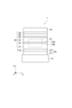
図1は、実施形態に係る磁気抵抗効果素子の積層方向に沿った断面を示す図である。磁気抵抗効果素子1は、例えば、基板10、下地層20、磁気抵抗層30、及びキャップ層40をこの順に備える。図1では、分かりやすく記載するために、積層方向(Z軸方向)における各層の厚さを拡大して磁気抵抗効果素子1を描いている。
Figure 1 is a diagram showing a cross section along the stacking direction of a magnetoresistance effect element according to an embodiment. The
基板10は、例えば、シリコン単結晶、金属酸化物単結晶、熱酸化珪素膜付シリコン単結晶、サファイア単結晶、セラミック、石英、及びガラスを含む。基板10に含まれる材料は、適度な機械的強度を有し、且つ熱処理や微細加工に適した材料であれば、特に限定されない。金属酸化物単結晶としては、例えば、MgO単結晶が挙げられ、MgO単結晶を含む基板によれば、例えば、スパッタ法を用いて容易にエピタキシャル成長膜が形成される。
The
下地層20は、磁気抵抗層30の結晶性を向上させるために設けられ、また、磁気抵抗効果素子1の磁気抵抗特性を測定するための電極として利用することができる。下地層20は、例えば、電極のための下部電極層21と、当該下部電極層21上に設けられたバッファ層22とを含む。
The
下部電極層21は、例えば、Al、Ag、Au、Cu、Cr、Pt、Ru、Ta、V、及びWのうち少なくとも一つの金属元素を含み、これらの金属元素の合金、又はこれら金属元素の2種類以上からなる材料の積層体を含んでもよい。金属元素の合金には、例えば、立方晶系のAgZn合金、AgMg合金及びNiAl合金が挙げられる。金属元素の2種類以上からなる材料の積層体には、例えば、TaとRuとを含む材料の積層体が挙げられる。具体的には、下部電極層21は、Ta、Ru、及びTaからなる3層積層体を含むことができる。
The
下部電極層21は上面21aを有し、上面21aに対しては、CMP研磨(Chemical Mechanical Polishing)を施すことができる。CMP研磨は、例えば、CMP装置を用いて、下部電極層21の上面21aが所望の粗さになるように当該上面21aを研磨する。CPM研磨の研磨時間によって、上面21aの粗さを制御すること可能である。一例では、CPM研磨の研磨時間が長くすることに従って、上面21aの粗さを低減させることができる。CPM研磨のためのスラリーには、例えば、アルミナが用いられる。
The
下部電極層21のZ軸方向の厚さは、例えば、10nm以上、かつ1000nm以下の範囲である。また、この厚さは、例えば、30nm以上、かつ150nm以下の範囲である。
The thickness of the
研磨後の下部電極層21は上面21a上にバッファ層22を積層することができて、バッファ層22は、例えば、下部電極層21と同様に、金属元素を含む。金属元素は、例えば、Al、Ag、Au、Cu、Cr、Pt、Ru、Ta、V、及びWの少なくとも一つであり、バッファ層22は、これらの金属元素の合金、又はこれら金属元素の2種類以上からなる材料の積層体を含んでもよい。金属元素の合金は、例えば、立方晶系のAgZn合金、AgMg合金及びNiAl合金である。バッファ層22は、具体的には、Ta及びRuからなる2層積層体を含むことができる。
The
バッファ層22のZ軸方向の厚さは、例えば、1nm以上、かつ10nm以下の範囲である。また、この厚さは、例えば、2nm以上、かつ5nm以下の範囲である。
The thickness of the
下地層20と基板10との間には、必要に応じて、上部の層の結晶配向を制御するための結晶配向層が設けられてもよい。結晶配向層は、例えば、MgO、TiN及びNiTa合金の少なくとも一種類を含む。
If necessary, a crystal orientation layer may be provided between the
磁気抵抗層30は、第一の強磁性層31と、第二の強磁性層32と、トンネルバリア層33と、反強磁性層34と、第三の強磁性層35と、磁気結合層36とを備える。トンネルバリア層33は、絶縁材料で構成され、第一の強磁性層31と第二の強磁性層32との間に積層される。反強磁性層34は、第二の強磁性層32のトンネルバリア層33側とは反対側に配置され、本実施形態では第三の強磁性層35上に積層される。第一の強磁性層31は、例えば、下地層20上に積層され、第一の強磁性層31、トンネルバリア層33、第二の強磁性層32、磁気結合層36、及び第三の強磁性層35は、この順に配列する。第一の強磁性層31は、磁化自由層として機能し、また、第二の強磁性層32、磁気結合層36、第三の強磁性層35及び反強磁性層34は、共同して磁化固定層として機能することができる。
The
磁化自由層として機能する第一の強磁性層31は、例えば、Fe、Co-Fe、Co-Fe-B及び強磁性のホイスラー合金等の軟磁気特性を有する強磁性材料で構成される。
The first
第一の強磁性層31のZ軸方向の厚さは、例えば、0.5nm以上、かつ100nm以下の範囲である。また、この厚さは、例えば、0.8nm以上、かつ20nm以下の範囲である。
The thickness of the first
本実施形態において、磁化固定層は、合成反強磁性(synthesized anti-ferro magnetic)構造(SAF構造)と呼ばれる構造を有する。即ち、磁気抵抗層30は、磁化固定層として、第二の強磁性層32及び反強磁性層34に加えて、第二の強磁性層32と反強磁性層34との間に設けられた第三の強磁性層35と、第二の強磁性層32と第三の強磁性層35との間に設けられた磁気結合層36を更に有する。第二の強磁性層32と第三の強磁性層35とは、磁気結合層36を介した交換結合によって、互いに反強磁性的に結合している。第三の強磁性層35は、第二の強磁性層32と同様の構成を有することができる。磁気結合層36は、例えばRu、Rh、又はIr等の非磁性金属で構成され、そのZ軸方向の厚さは、例えば、0.3nm以上、かつ2nm以下の範囲である。本実施形態において、磁化固定層は、必要に応じて、SAF構造を有しなくてもよい。この場合、磁化固定層は、磁気結合層36及び第三の強磁性層35を有さず、反強磁性層34は第二の強磁性層32の上に直接積層される。
In this embodiment, the magnetization pinned layer has a structure called a synthetic anti-ferromagnetic structure (SAF structure). That is, the
磁化固定層の第二の強磁性層32及び第三の強磁性層35の磁化方向は、磁化自由層として機能する第一の強磁性層31の磁化方向に比べて、外部磁界に対して変化し難い。第二の強磁性層32及び第三の強磁性層35の磁化方向は、測定対象の外部磁界等の使用中に印加され得る外部磁界に対して実質的に固定されており、当該外部磁界に対して実質的に変化しないことが好ましい。本実施形態では、このような第二の強磁性層32及び第三の強磁性層35の磁化方向の態様を、反強磁性層34と第三の強磁性層35とを交換結合させて、第三の強磁性層35に直接的に、第二の強磁性層32に間接的に一方向磁気異方性を付与することによって実現している。当該磁化方向の態様は、反強磁性層34を用いずに実現することも可能であるため、磁気抵抗層30は反強磁性層34を有していなくてもよい。磁化固定層がSAF構造を有さない場合も、同様の理由で磁気抵抗層30は反強磁性層34を有していなくてもよい。一方、磁化自由層として機能する第一の強磁性層31は、例えば、軟磁性材料で構成され、磁化方向が実質的に固定されていない。そのため、磁気抵抗層30に外部磁界が印加されると、その方向に磁化方向が容易に変化する。磁気抵抗層30に外部磁場が印加され、第一の強磁性層31及び第二の強磁性層32の相対的な磁化方向が変化することによって、磁気抵抗層30の抵抗値が変化して、磁気抵抗効果素子1が磁気抵抗効果を発揮する。
The magnetization directions of the second
第二の強磁性層32及び第三の強磁性層35は、強磁性材料で構成されることができる。磁化固定層のための強磁性材料としては、例えば、Ni、Fe、Ru、Mn、Ir、及びCoのうち少なくとも一種の元素を有する金属または合金が挙げられる。合金の具体例としては、Co-Fe合金、Ni-Fe合金、Co-B合金、Fe-B合金又はCo-Fe-B合金等が挙げられる。Co-Fe-Al合金、Co-Fe-Si合金、Co-Mn-Si合金、Co-Mn-Ge合金、Co-Fe-Al-Si合金、及びCo-Fe-Ga-Ge合金といったホイスラー合金が挙げられる。第二の強磁性層32は、例えば、Co-Fe-B合金及びCo-Fe合金などの多層膜が繰り返し積層された構造を有することができる。
The second
第二の強磁性層32のZ軸方向の厚さは、例えば、2nm以上、かつ10nm以下の範囲である。また、この厚さは、例えば、3nm以上、かつ7nm以下の範囲である。第三の強磁性層35のZ軸方向の厚さは、例えば、1nm以上、かつ8nm以下の範囲である。また、この厚さは、例えば、2nm以上、かつ6nm以下の範囲である。
The thickness of the second
反強磁性層34は、例えば、FeMn合金、PtMn合金、PtCrMn合金、NiMn合金、IrMn合金、NiO、Fe2O3等の反強磁性材料で構成される。
The
反強磁性層34のZ軸方向の厚さは、例えば、5nm以上、かつ20nm以下の範囲である。
The thickness of the
磁気抵抗層30においては、第一の強磁性層31及び第二の強磁性層32の一方が磁化自由層として機能し、他方が磁化固定層の一部として機能すればよい。このため、本実施形態の変形例として、第一の強磁性層31が磁化固定層の一部として機能し、第二の強磁性層32が単独で磁化自由層として機能してもよい。この場合、反強磁性層34は、第一の強磁性層31のトンネルバリア層33側とは反対側に直接又はSAF構造を構成するように磁気結合層36及び第三の強磁性層35を介して設けられ、第一の強磁性層31に直接的又は間接的に一方向磁気異方性を付与する。
In the
磁気抵抗効果素子1は、磁気抵抗層30上にキャップ層40を備えることができる。キャップ層40は、磁気抵抗層30を保護するために設けられる。キャップ層40は、例えば、Ru、Ag、Al、Cu、Au、Cr、Mo、Pt、W、Ta、Pd、及びIrの一以上の金属元素、これら金属元素の合金、又は、これら金属元素の2種類以上からなる材料の積層体を含んでよい。必要に応じて、キャップ層40上には、磁気抵抗効果素子1にZ軸方向に沿って電流を流すための上部電極を設けてもよい。
The
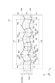
図2は、図1に示される領域E1の一例を拡大して示す図であり、磁気抵抗層30の積層方向(Z軸方向)に沿った断面のうちの一つの例を示す図である。図2に示されるように、トンネルバリア層33は、上面33aと、上面33aの反対側に位置する下面33bとを有する。上面33aは、第二の強磁性層32側に位置し、下面33bは、第一の強磁性層31側に位置することができる。トンネルバリア層33の上面33aは、表面粗さを有する。上面33aは、当該表面粗さに起因して、例えば、一つ又は複数の突起33cと一つ又は複数の窪み33dとを有する。
2 is an enlarged view of an example of region E1 shown in FIG. 1, showing an example of a cross section along the stacking direction (Z-axis direction) of the
トンネルバリア層33の上面33aは、上記表面粗さとしての最大高さ粗さRz1を有する。この最大高さ粗さRz1は、JISB 0601:2013規格によって規定される。この規格に従い、上面33aの最大高さ粗さRz1は、上面33aの粗さ曲線のうちの基準長さLr1の範囲内において、平均線Av1(基準長さLr1の範囲内における上面33aの粗さ曲線の算術平均高さ)から最も高い突起33cの高さRp1と、平均線Av1から最も低い窪み33dの深さRv1との和の値として定義される。上面33aの上記粗さ曲線は、例えば、TEM(透過電子顕微鏡)、STEM(走査型透過電子顕微鏡)、SEM(走査電子顕微鏡)又はAFM(原子間力顕微鏡)によって測定される。基準長さLr1は、磁気抵抗層30の面内方向(XY面内方向)に沿った方向の所定の長さであり、例えば、4nm、8nm、10nm、20nm、又は30nmである。
The
トンネルバリア層33の下面33bは、上面33aと同様に、表面粗さを有し、当該表面粗さに起因して、例えば、一つ又は複数の突起33fと一つ又は複数の窪み33gとを有する。下面33bの最大高さ粗さRz2は、上面33aの最大高さ粗さRz1と同様に、JISB 0601:2013規格によって規定される。最大高さ粗さRz2は、下面33bの粗さ曲線のうちの基準長さLr2の範囲内において、平均線Av2から最も高い突起33fの高さRp2と、平均線Av2から最も低い窪み33gの深さRv2との和の値として定義される。下面33bの上記粗さ曲線も、TEMなどによって測定され、基準長さLr2は、磁気抵抗層30の面内方向に沿って、例えば、4nm、8nm、10nm、20nm、又は30nmである。図2は、基準長さLr1が基準長さLr2と同じ長さである例を図示しているが、基準長さLr1は、基準長さLr2と異なる長さであってもよい。
The
磁気抵抗効果素子1においては、トンネルバリア層33の上面33aの最大高さ粗さRz1及び下面33bの最大高さ粗さRz2のうち、より大きな最大高さ粗さをRzとすることができる。トンネルバリア層33の上面33aが最大高さ粗さRzを有してもよいし、下面33bが最大高さ粗さRzを有してもよい。上面33aの最大高さ粗さRz1が下面33bの最大高さ粗さRz2と同じであるときには、上面33a及び下面33bが、共に最大高さ粗さRzを有してもよい。トンネルバリア層33の上面33a及び/又は下面33bが最大高さ粗さRzを有する。図2では、下面33bよりも上面33aの方がより大きな最大高さ粗さRzを有する場合を示している。
In the
トンネルバリア層33のZ軸方向の厚さをtとしたとき、Z軸方向に沿った磁気抵抗層30の断面のうちの少なくとも1つの断面において、Rz/t<1である。トンネルバリア層33のZ軸方向の厚さtは、上面33aの最大高さ粗さRz1が、最大高さ粗さRzであるときには、例えば、基準長さLr1の範囲内においてトンネルバリア層33のZ軸方向の厚さを算術平均することによって求められる。トンネルバリア層33のZ軸方向の厚さtは、例えば、TEM(透過電子顕微鏡)、STEM(走査型透過電子顕微鏡)又はSEM(走査電子顕微鏡)によって測定される。トンネルバリア層33のZ軸方向の厚さtは、下面33bの最大高さ粗さRz2が、最大高さ粗さRzであるときには、例えば、基準長さLr2の範囲内においてトンネルバリア層33のZ軸方向の厚さを算術平均することによって求められる。
When the thickness of the
本実施形態では、磁気抵抗層30のZ軸方向に沿った断面のうち、少なくとも互いに直交する2つの断面においてRz/t<1であることが好ましく、磁気抵抗層30のZ軸方向に沿った実質的に全ての断面においてRz/t<1であることがさらに好ましい。
In this embodiment, it is preferable that Rz/t<1 in at least two mutually perpendicular cross sections of the
トンネルバリア層33の上面33a及び下面33bの表面粗さは、磁気抵抗効果素子1のトンネルバリア層33よりも下方の要素の上面(例えば、下部電極層21の上面21a(図1参照))の表面粗さにも起因する。そのため、トンネルバリア層33の最大高さ粗さRzの大きさは、当該要素の上面(例えば上面21a)の表面粗さ(例えば最大高さ粗さ)を制御することによって、所定の大きさに制御することができる。トンネルバリア層33の最大高さ粗さRzの大きさは、当該要素の上面の最大高さ粗さの大きさと比較して、同程度であってもよいし、大きくてもよいし、小さくてもよい。
The surface roughness of the
トンネルバリア層33の最大高さ粗さRzは、例えば0.2nm以上、3.2nm以下であることが好ましく、0.6nm以上、1.8nm以下であることがさらに好ましい。トンネルバリア層33のZ軸方向の厚さは、例えば1nm以上、3.2nm以下であることが好ましく、1.6nm以上、2.2nm以下であることがさらに好ましい。
The maximum height roughness Rz of the
図2に示されるように、トンネルバリア層33は、少なくとも一つのアモルファス領域61と、少なくとも一つの結晶化領域62とを含む。アモルファス領域61と結晶化領域62とは、互いに、例えば、境界33eによって区分けされることができる。トンネルバリア層33は、実質的に少なくとも一つのアモルファス領域61と少なくとも一つの結晶化領域62のみで構成されてもよい。アモルファス領域61と結晶化領域62は、実質的に同じ組成を有するが、実質的に異なる組成を有していてもよい。
2, the
アモルファス領域61は、トンネルバリア層33内に少なくとも一つ含まれる。アモルファス領域61の数は、トンネルバリア層33全体の中において、例えば、2であってよく、また、5であってもよい。結晶化領域62は、トンネルバリア層33内に少なくとも一つ含まれる。結晶化領域62の数は、トンネルバリア層33全体の中において、例えば、2であってよく、また、5であってもよい。トンネルバリア層33全体の中において、アモルファス領域61の数と、結晶化領域62の数とは、互いに同一であってもよく、互いに異なっていてもよい。
At least one
トンネルバリア層33の結晶構造の特定には、TEMおよびSTEMを使った局所電子回折法を用いることができる。局所電子回折法は、ナノメートルスケールまで電子線を絞った場合はナノビーム電子回折法、サブナノメートルスケールまで電子線を絞った場合はオングストローム電子回折法と呼ばれることもある。トンネルバリア層33の局所的な領域が結晶化している場合、対応する電子回折像はスポットパターンとなり、トンネルバリア層33の局所的な領域がアモルファスの場合は、対応する電子回折像はハローパターンとなる。そのため、局所電子回折法によれば、トンネルバリア層33の局所的な領域が結晶化しているか、又はアモルファス化しているかを判別することができる。
To identify the crystal structure of the
上述のような磁気抵抗効果素子1においては、トンネルバリア層33の上面33a及び/又は下面33bが最大高さ粗さRzを有する。そのため、上面33a及び/又は下面33bが実質的に平坦である場合と比較して、上面33a及び/又は下面33bの面積が増加するため、磁気抵抗効果素子1のRA(XY平面における単位面積当たりの抵抗値)が高くなる。さらに、トンネルバリア層33が、少なくとも一つのアモルファス領域61を含むため、当該領域が結晶化している場合と比較して、磁気抵抗効果素子1のRAが高くなる。また、トンネルバリア層33においてRz/t<1が満たされるため、トンネルバリア層33の厚さtに対して上面33aの最大高さ粗さRzが過剰となることに起因するMR比の低減を防止できる。これにより、本実施形態の磁気抵抗効果素子1によれば、MR比の低減を抑制しつつ、高いRAを実現することができる。
In the
本実施形態の磁気抵抗効果素子1のトンネルバリア層33において、0.1<Rz/tであることが好ましく、0.32<Rz/tであることがさらに好ましい。これにより、上面33aの面積が十分に増加するため、磁気抵抗効果素子1のRAを十分に高くすることができる。このRz/tの下限値に関する条件は、上述のRz/tの上限値に関する条件と同様に、Z軸方向に沿った磁気抵抗層30の断面のうちの少なくとも1つの断面において満たされればよく、磁気抵抗層30のZ軸方向に沿った断面のうち、少なくとも互いに直交する2つの断面において満たされることが好ましく、磁気抵抗層30のZ軸方向に沿った実質的に全ての断面において満たされることがさらに好ましい。
In the
図2では、トンネルバリア層33内において、アモルファス領域61と結晶化領域62とが、トンネルバリア層33の概ね面内方向(XY面内方向)に並んだ例が示されているが、アモルファス領域61と結晶化領域62とは、積層方向(Z軸方向)に並んでもよい。例えば、トンネルバリア層33内において、アモルファス領域61の上に結晶化領域62が並んでいてもよく、例えば、アモルファス領域61、結晶化領域62、及びアモルファス領域61がこの順に積層方向に並んでいてもよい。
2 shows an example in which the
トンネルバリア層33のZ軸方向に沿った断面のうちの少なくとも1つの断面(好ましくはトンネルバリア層33のZ軸方向に沿った断面のうち、少なくとも互いに直交する2つの断面、さらに好ましくはトンネルバリア層33のZ軸方向に沿った実質的に全ての断面)において、トンネルバリア層33全体の面積に占める少なくとも一つの結晶化領域62の面積の割合は、5%より大きく、かつ、65%より小さいことが好ましく、20%より大きく、かつ、50%より小さいことがさらに好ましい。
In at least one cross section of the
当該面積割合が5%(好ましくは20%)より大きい場合、アモルファス領域61の割合が過大となることに基づくMR比の低減を抑制できる。また、当該面積の割合が65%(好ましくは50%)より小さい場合、アモルファス領域61の割合が十分に大きくなるため、トンネルバリア層33の一部を結晶化させるためのプロセス処理により生じるおそれのある第一の強磁性層31及び第二の強磁性層32の少なくとも一つの劣化によるMR比の低減が防止されると共に、RAが十分に高くなる。少なくとも1つの結晶化領域62の当該面積の割合は、例えば、トンネルバリア層33を形成する際に行うアニール工程のアニール温度によって制御されることができ、少なくとも1つのアモルファス領域61の当該面積の割合に比べて、大きくてもよく、ほぼ等しくてもよく、また、小さくてもよい。
When the area ratio is greater than 5% (preferably 20%), the reduction in the MR ratio due to the proportion of the
面内方向に沿った少なくとも1つの断面においても、トンネルバリア層33全体の面積に占める少なくとも一つのアモルファス領域61の面積の割合は、トンネルバリア層33全体の面積に占める少なくとも一つの結晶化領域62の面積の割合に比べて、大きくてもよく、ほぼ等しくてもよく、また、小さくてもよい。本実施形態では、少なくとも一つの結晶化領域62の当該面積の割合は、5%より大きく、かつ、65%より小さいことが好ましく、20%より大きく、かつ、50%より小さいことがさらに好ましい。
In at least one cross section along the in-plane direction, the ratio of the area of at least one
少なくとも一つのアモルファス領域61は、トンネルバリア層33の面内方向に沿った幅W61を有し、少なくとも一つの結晶化領域62は、トンネルバリア層33の面内方向に沿った幅W62を有する。アモルファス領域61の幅W61は、例えば、1nm以上、30nm以下であり、結晶化領域62の幅W62は、例えば、0.15nm以上、8nm未満である。本実施形態において、幅W61及び幅W62は、共に、面内方向(XY面内方向)に沿って規定される幅の最大値を示す。図2は、幅W61及び幅W62が、共にX軸方向に沿った幅の最大値である例を示している。
At least one
磁気抵抗効果素子1では、結晶化領域62の幅W62が8nm未満であってもよいので、トンネルバリア層33の結晶化領域62において、トンネルバリア層33と、第一の強磁性層31及び第二の強磁性層32の少なくとも一つとの格子不整合が生じた場合も、格子不整合が生じる領域を小さくすることができる。その結果、磁気抵抗効果素子1は、より高いMR比を有することができる。当該効果は、結晶化領域62の幅W62が5nm未満であるとき、より顕著に発揮される。
In the
少なくとも一つのアモルファス領域61は、Z軸方向に沿った高さH61を有し、少なくとも一つの結晶化領域62は、Z軸方向に沿った高さH62を有する。アモルファス領域61の高さH61は、例えば、0.2nm以上、3nm以下であり、結晶化領域62の高さH62は、例えば、0.2nm以上、3nm以下である。
At least one
本実施形態では、少なくとも一つの結晶化領域62は、Z軸方向に(001)面が配向した結晶構造を有してもよい。磁気抵抗効果素子1は、この(001)面が配向した結晶化領域62によって、高いコヒーレントトンネル効果を得ることができて、その結果、高いMR比を有することができる。この効果は、結晶化領域62が、MgO、MgAl2O4、γ-アルミナで構成されるときに、特に顕著に発揮される。
In this embodiment, at least one
少なくとも一つの結晶化領域62の少なくとも一部は、第一の強磁性層31及び第二の強磁性層32の少なくとも一つと格子整合してもよい。これにより、高いコヒーレントトンネル効果を得ることができる。磁気抵抗効果素子1は、より高いMR比を有することができる。磁気抵抗効果素子1において、結晶化領域62が第一の強磁性層31及び第二の強磁性層32と格子整合していることは、例えば、構造観察によって得られた格子像を逆フーリエ変換した像によって確認できる。
At least a portion of at least one
トンネルバリア層33は、次の式(1)で表されるスピネル構造を有する酸化物材料を含むことができる。
A1-xBxOy …(1)
式(1)中、Aは、Mg、Zn、Cu、Cd、Li、Ni、Co、Fe、Mn、Cr、Hg、及びVからなる群より選択される少なくとも一種の元素を表し、Bは、Al、Ga、In、Sc、Ti、V、Cr、Mn、Fe、Rh、Ir、Ge、及びCoからなる群より選択される少なくとも一種の元素を表す。また、0<x≦1、及び、0.35≦y≦1.7であり、Oは酸素を表す。尚、上記スピネル構造には、式(1)のAとBとの原子配列が不規則化した不規則化スピネル構造も含まれる。
The
A 1-x B x O y ... (1)
In formula (1), A represents at least one element selected from the group consisting of Mg, Zn, Cu, Cd, Li, Ni, Co, Fe, Mn, Cr, Hg, and V, and B represents at least one element selected from the group consisting of Al, Ga, In, Sc, Ti, V, Cr, Mn, Fe, Rh, Ir, Ge, and Co. In addition, 0<x≦1 and 0.35≦y≦1.7, and O represents oxygen. The spinel structure also includes a disordered spinel structure in which the atomic arrangement of A and B in formula (1) is disordered.
この場合、トンネルバリア層33の結晶化領域62において、第一の強磁性層31及び第二の強磁性層32との格子不整合をより小さくすることができる。何故なら、トンネルバリア層33の結晶化領域62の格子定数と、第一の強磁性層31及び第二の強磁性層32の格子定数とのミスマッチを小さくすることができるからである。
In this case, the lattice mismatch between the crystallized
式(1)において、Aは、Mgを表し、Bは、Alを表してもよい。この構成によって、トンネルバリア層33が大きなMR比を実現するための機能を十分に発揮できる。
In formula (1), A may represent Mg and B may represent Al. This configuration allows the
また、式(1)において、0<x<0.5であってもよい。これにより、トンネルバリア層33が大きなMR比を実現するための機能を更に十分に発揮できる。
Also, in formula (1), 0<x<0.5 may be satisfied. This allows the
また、式(1)において、0<x<0.5、及び、1≦y≦1.33であってもよい。この場合、トンネルバリア層33が大きなMR比を実現するための機能を更に十分に発揮できる。
In addition, in formula (1), 0<x<0.5 and 1≦y≦1.33 may be satisfied. In this case, the
トンネルバリア層33は、上述の式(1)で表されるスピネル構造を有する酸化物材料の他に、MgOまたはγ-アルミナで構成されることができる。
The
磁気抵抗層30では、第一の強磁性層31、第二の強磁性層32、及びトンネルバリア層33の少なくとも一つは、双晶を含んでもよい。これにより、トンネルバリア層33の上面33a及び下面33bが粗さを有することに起因してこれらの層の界面近傍に生じ得る歪を、この双晶によって緩和することができる。その結果、トンネルバリア層33と、第一の強磁性層31及び/又は第二の強磁性層32との界面における格子歪が緩和される。
In the
上記双晶は、面心立方格子構造を有し、その双晶面は、(111)面である、又は上記双晶は体心立方格子構造を有し、その双晶面は、(112)面であってもよい。双晶が、当該双晶の結晶構造の種類に応じて適切な双晶面を有することができるので、トンネルバリア層33と、第一の強磁性層31及び/又は第二の強磁性層32との界面における格子歪がさらに緩和される。磁気抵抗効果素子1は、より高いMR比を有することができる。
The twin may have a face-centered cubic lattice structure and the twin plane may be a (111) plane, or the twin may have a body-centered cubic lattice structure and the twin plane may be a (112) plane. Since the twin can have an appropriate twin plane depending on the type of crystal structure of the twin, the lattice distortion at the interface between the
第一の強磁性層31及び第二の強磁性層32の少なくとも一つは、トンネルバリア層33と接するCozFe100-z(0<z<80)からなる領域を有してもよい。これにより、当該領域のスピン分極率が高くなると共に、当該領域とトンネルバリア層33との間の格子不整合を小さくすることができる。
At least one of the first
図3は、図1に示される領域E1の他の例を拡大して示す図であり、磁気抵抗層30の積層方向(Z軸方向)に沿った断面のうちの一つの他の例を示す図である。
Figure 3 is an enlarged view of another example of region E1 shown in Figure 1, showing another example of a cross section along the stacking direction (Z-axis direction) of the
図3に示すトンネルバリア層33は、アモルファス領域61と結晶化領域62との間に介在領域63をさらに有する点において、図2に示すトンネルバリア層33と異なる。介在領域63は、トンネルバリア層33を構成する材料のうち、結晶化もアモルファス化もしていない材料で構成される。アモルファス領域61と介在領域63とは、互いに、例えば、境界61aによって区分けされ、結晶化領域62と介在領域63とは、互いに、例えば、境界62aによって区分けされることができる。
The
図3のトンネルバリア層33は、アモルファス領域61と結晶化領域62との間に介在領域63を有することを除いて、図2のトンネルバリア層33と同様の構造を有することができる。図3のトンネルバリア層33は、上面33aと、上面33aの反対側に位置する下面33bとを有する。トンネルバリア層33の上面33aは、表面粗さとしての最大高さ粗さRz1を有する。上面33aは、当該表面粗さに起因して、例えば、一つ又は複数の突起33cと一つ又は複数の窪み33dとを有する。トンネルバリア層33の下面33bは、上面33aと同様に、表面粗さを有し、当該表面粗さに起因して、例えば、一つ又は複数の突起33fと一つ又は複数の窪み33gとを有する。
3 may have a structure similar to that of the
本実施形態において、磁気抵抗効果素子1は、例えば、スパッタ法及び電子ビーム蒸着法といった製造方法によって基板10上に下地層20からキャップ層40までの各層を形成することにより作製される。各層の形成時には、必要に応じて熱処理を行っても良いし、また、さらに必要に応じて、一方向磁気異方性を付与するための磁場印加処理を行っても良い。磁場印加処理の際には適宜熱処理を同時に行っても良い。また、磁気抵抗効果素子1は、電子線等を用いたリソグラフィーおよびArイオン等を用いたドライエッチングにより、磁気抵抗特性を評価可能な形状に微細加工されてもよい。磁気抵抗効果素子1は、積層方向(各層の膜面に垂直な方向、Z軸方向)に沿って検出用電流が流されるCPP(Current Perpendicular to Plane)構造の磁気抵抗効果素子である。
In this embodiment, the
本実施形態に係る磁気抵抗効果素子を製造する方法は、下地層20上に第一の強磁性層31を形成する工程と、第一の強磁性層31上にトンネルバリア層33を形成する工程と、トンネルバリア層33上に第二の強磁性層32を形成する工程とを有する。
The method for manufacturing the magnetoresistance effect element according to this embodiment includes the steps of forming a first
第一の強磁性層31を形成する工程は、スパッタ法によって実行することができて、この工程では、下地層20上に、例えば、CoFeB層及びCoFe層からなる2層積層体が形成される。
The process of forming the first
トンネルバリア層33を形成する工程は、例えばスパッタ法によって、第一の強磁性層31上にMgAl合金層を形成する工程と、このMgAl合金層を酸化して、少なくとも一つのアモルファス領域61と、例えばMg1-xAlxOy(0<x≦1、0.35≦y≦1.7)で表されるスピネル構造からなる少なくとも一つの結晶化領域62とを含むトンネルバリア層33を形成する工程とを含む。この工程によって形成されたトンネルバリア層33において、その上面33aの最大高さ粗さRz1及び下面33bの最大高さ粗さRz2のうち、より大きな最大高さ粗さをRzとし、トンネルバリア層33の厚さをtとしたとき、積層方向に沿った断面において、Rz/t<1である。
The process of forming the
また、上記MgAl合金層を酸化する工程は、ラジカル酸化、プラズマ酸化、オゾン酸化、及び自然酸化の少なくとも一つによって上記MgAl層を酸化する工程を含むことができる。この場合、上述のような所定の態様のトンネルバリア層33を効率よく形成することができる。
The step of oxidizing the MgAl alloy layer may include a step of oxidizing the MgAl layer by at least one of radical oxidation, plasma oxidation, ozone oxidation, and natural oxidation. In this case, the
第二の強磁性層を形成する工程は、例えば、スパッタ法によって行われ、この工程では、トンネルバリア層33上に、例えば、CoFe層、CoFeB層及びCoFe層からなる3層積層体が形成される。
The process of forming the second ferromagnetic layer is performed, for example, by a sputtering method, and in this process, for example, a three-layer stack consisting of a CoFe layer, a CoFeB layer, and a CoFe layer is formed on the
この磁気抵抗効果素子を作製する方法によれば、MR比の低減を抑制しつつ、高いRAを有する磁気抵抗効果素子1を製造できる。
This method for manufacturing a magnetoresistance effect element makes it possible to manufacture a
以下、本発明の実施例および比較例により、さらに磁気抵抗効果素子について説明するが、本発明は下記例に制限されない。 The magnetoresistance effect element will be further described below with examples and comparative examples of the present invention, but the present invention is not limited to the following examples.
(実施例1)
実施例1として、図1に示す実施形態の磁気抵抗効果素子1と同様の構成を有する磁気抵抗効果素子を作製した。実施例1に係る説明では、磁気抵抗効果素子1に係る説明のために用いられた符号を援用する。なお、実施例2以降の実施例、及び比較例においても、同様に、磁気抵抗効果素子1に係る説明のために用いられた符号を援用する。
Example 1
As Example 1, a magnetoresistance effect element having a configuration similar to that of the
実施例1では、以下のような手順によって磁気抵抗効果素子1を作製した。初めに、Siからなる基板10を準備した。基板10上には、熱酸化珪素膜を設けた。熱酸化珪素膜が設けられた基板10を、マグネトロンスパッタ装置内に設置し、下地層20の下部電極層21を形成した。下部電極層21は、Ta層(厚さ5nm)、Ru層(厚さ100nm)、及びTa層(厚さ30nm)をこの順に積層した3層積層体からなる。下部電極層21の形成時の温度は、室温とした。
In Example 1, the
下部電極層21を形成した基板10をマグネトロンスパッタ装置から取り出して、CMP装置に設置した。CMP装置を用いて、下部電極層21の上面が所望の粗さになるように、当該上面を研磨した。研磨のためのスラリーには、アルミナを用いた。研磨時間は、60秒とした。
The
CMP研磨の後、基板10をマグネトロンスパッタ装置内に再び設置し、スパッタ法によって、研磨後の下部電極層21上にバッファ層22を形成した。バッファ層22は、Ta層(厚さ2nm)及びRu層(厚さ2nm)からなる2層積層体とした。バッファ層22の形成時の温度は、室温とした。
After the CMP polishing, the
次に、下地層20のバッファ層22上に、スパッタ法によって磁気抵抗層30を形成した。磁気抵抗層30の形成では、初めに、磁化自由層としての第一の強磁性層31を形成した。第一の強磁性層31は、CoFeB層(厚さ3nm)及びCoFe層(厚さ1nm)からなる2層積層体とした。第一の強磁性層31の形成時の温度は、室温とした。第一の強磁性層31を形成した後の熱処理は行わなかった。
Next, a
続いて、第一の強磁性層31上に、トンネルバリア層33を形成した。トンネルバリア層33の形成では、初めに、第一の強磁性層31上にMgAl合金層を形成し、続いて、MgAl合金層を酸化した。MgAl合金層の形成は、スパッタ法によって行い、MgAl合金層の酸化は、自然酸化によった。アニール処理(温度300℃)を15分間行った後、MgAl2O4からなるトンネルバリア層33が作製された。トンネルバリア層33の厚さtは、1.80nmとした。
Next, a
次に、トンネルバリア層33上に、SAF構造の磁化固定層を形成した。磁化固定層は、第二の強磁性層32としてのCoFe層(厚さ1nm)、CoFeB層(厚さ3nm)及びCoFe層(厚さ1nm)からなる3層積層体、磁気結合層36としてのRu層(厚さ0.8nm)、第三の強磁性層35としてのCoFe層(厚さ3nm)、及び反強磁性層34としてのIrMn層(厚さ8nm)からなる多層積層体とした。磁化固定層の形成時の温度は、室温とした。磁化固定層を形成した後の熱処理は行わなかった。磁化固定層の形成によって、磁気抵抗層30が作製された。
Next, a magnetization pinned layer of an SAF structure was formed on the
磁気抵抗層30の作製後、磁気抵抗層30の磁化固定層上に、キャップ層40を形成した。キャップ層40は、Ru層(厚さ3nm)及びTa層(厚さ5nm)を含む2層積層体とした。キャップ層40の形成時の温度は、室温とした。キャップ層40を形成した後の熱処理は行わなかった。
After the
キャップ層40の形成後に、磁場中熱処理を行い、反強磁性層34としてのIrMn層と第三の強磁性層35とを交換結合させることにより、第三の強磁性層35としてのCoFe層及び第二の強磁性層32としてのCoFe層、CoFeB層及びCoFe層からなる3層積層体に対して一方向磁気異方性を付与した。この磁場中熱処理においては、熱処理温度を300℃とし、熱処理時間を3時間とし、印加磁場の強度を10kOe(798kA/m)とした。この磁場中熱処理によって、実施例1に係る磁気抵抗効果素子1の作製が完了した。
After the
(MR比の測定)
図4は、実施例1に係る磁気抵抗効果素子のMR比を測定できる磁気抵抗デバイスを示す図である。磁気抵抗デバイス50は、第1電極層51と、当該第1電極層51と共に磁気抵抗効果素子1を挟む第2電極層52とを備える。磁気抵抗効果素子1は、磁気抵抗特性の測定に適する形状に微細加工した。第1電極層51が磁気抵抗効果素子1の基板10上の下地層20に接続され、第2電極層52が磁気抵抗効果素子1のキャップ層40に接続されている。磁気抵抗デバイス50は、電源53と電圧計54とを更に備え、電源53及び電圧計54が、共に、第1電極層51及び第2電極層52に接続されている。電源53によって磁気抵抗効果素子1に積層方向に電流を印加し、この際の磁気抵抗効果素子1への印加電圧を電圧計54によってモニターすることができる。本実施例では、磁気抵抗効果素子1に積層方向に一定電流を流した状態で、外部から磁気抵抗効果素子1に磁場を掃引しながら磁気抵抗効果素子1への印加電圧を電圧計54によってモニターすることにより、磁気抵抗効果素子1の抵抗変化を測定した。
(Measurement of MR ratio)
FIG. 4 is a diagram showing a magnetoresistance device capable of measuring the MR ratio of the magnetoresistance effect element according to the first embodiment. The
本実施例では、抵抗変化の測定結果から、磁気抵抗効果素子1のMR比を算出した。MR比は、百分率で示され、下記の式(i)によって算出できる。
MR比(%)=((RAP-RP)/RP)×100(%) …(i)
この式(i)において、RAPは、第一の強磁性層31の磁化の向きと第二の強磁性層32の磁化の向きとが反平行であるときの磁気抵抗効果素子1の抵抗の大きさである。また、RPは、第一の強磁性層31の磁化の向きと第二の強磁性層32の磁化の向きとが平行であるときの磁気抵抗効果素子1の抵抗の大きさである。後述の他の実施例及び比較例においても、同様にMR比の測定を行った。
In this example, the MR ratio of the
MR ratio (%)=(( RAP - RP )/ RP )×100(%) (i)
In this formula (i), R AP is the magnitude of the resistance of the
(RAの測定)
実施例1では、磁気抵抗デバイス50を用いて、磁気抵抗効果素子1の抵抗変化を測定し、その測定結果から、磁気抵抗効果素子1のRA(面積抵抗)を測定した。本実施例では、磁気抵抗効果素子1の平面視形状の面積をAとしたとき、式(i)のRpに対して、Aを乗じたRpAをRA(面積抵抗)と規定した。RAは、印加されるバイアス電圧を磁気抵抗効果素子1の積層方向に流れた電流で割ることによって得られる抵抗値を、各層が接合される面の面積の逆数で割り、単位面積における抵抗値に規格化した数値である。RA(面積抵抗)の値は、3%以内の測定誤差を含む。後述の他の実施例及び比較例においても、同様にRAの測定を行った。
(Measurement of RA)
In Example 1, the
(最大高さ粗さRzの測定)
本実施例では、積層方向に沿った断面のTEM観察によって、トンネルバリア層33の上面33aの最大高さ粗さRz1及び下面33bの最大高さ粗さRz2を測定した。これらの最大高さ粗さRz1及び最大高さ粗さRz2の測定は、JISB 0601:2013規格に従って行い、基準長さLr1及び基準長さLr2は、共に、20nmとした。本実施例では、トンネルバリア層33の上面33aの最大高さ粗さRz1及び下面33bの最大高さ粗さRz2のうち、上面33aの最大高さ粗さRz1がより大きな最大高さ粗さを示したので、上面33aの最大高さ粗さRz1を最大高さ粗さRzとした。後述の他の実施例及び比較例においても、同様に最大高さ粗さRzの測定を行った。これら他の実施例及び比較例においても、上面33aの最大高さ粗さRz1がより大きな最大高さ粗さを示したので、上面33aの最大高さ粗さRz1を最大高さ粗さRzとした。
(Measurement of maximum height roughness Rz)
In this example, the maximum height roughness Rz1 of the
(結晶化領域の割合の見積り)
本実施例では、積層方向に沿った断面のTEM観察によって、トンネルバリア層33における結晶化領域62の割合を見積もった。後述の他の実施例及び比較例においても、同様に結晶化領域62の割合の測定を行った。
(Estimation of the percentage of crystallized regions)
In this example, the ratio of the crystallized
(実施例2)
実施例2では、下部電極層21の上面をCMP研磨した研磨時間を30秒としたこと、及びトンネルバリア層33の厚さtを1.81nmとしたことを除いて、実施例1と同様の方法で同様の構成に形成した磁気抵抗効果素子1を作製した。
Example 2
In Example 2, a
(実施例3)
実施例3では、下部電極層21の上面をCMP研磨した研磨時間を15秒としたこと、及びトンネルバリア層33の厚さtを1.79nmとしたことを除いて、実施例1と同様の方法で同様の構成に形成した磁気抵抗効果素子1を作製した。
Example 3
In Example 3, a
(実施例4)
実施例4では、トンネルバリア層33の厚さtを2.00nmとしたことを除いて、実施例1と同様の方法で同様の構成に形成した磁気抵抗効果素子1を作製した。
Example 4
In the fourth embodiment, a
(実施例5)
実施例5では、下部電極層21の上面をCMP研磨した研磨時間を30秒としたこと、及びトンネルバリア層33の厚さtを2.01nmとしたことを除いて、実施例1と同様の方法で同様の構成に形成した磁気抵抗効果素子1を作製した。
Example 5
In Example 5, a
(実施例6)
実施例6では、下部電極層21の上面をCMP研磨した研磨時間を15秒としたこと、及びトンネルバリア層33の厚さtを1.96nmとしたことを除いて、実施例1と同様の方法で同様の構成に形成した磁気抵抗効果素子1を作製した。
Example 6
In Example 6, a
(実施例7)
実施例7では、トンネルバリア層33の材料と厚さとが異なることを除いて、実施例1と同様の方法で同様の構成に形成した磁気抵抗効果素子1を作製した。
(Example 7)
In the seventh embodiment, a
トンネルバリア層33の形成は、初めに、第一の強磁性層31上にMg層を形成し、続いて、当該Mg層を酸化した。Mg層の形成は、スパッタ法によって行い、Mg層の酸化は、自然酸化によって行った。アニール処理(温度250℃)を15分間行った後、MgOからなるトンネルバリア層33を作製した。トンネルバリア層33の厚さtは、1.79nmとした。
The
(実施例8)
実施例8では、下部電極層21の上面をCMP研磨した研磨時間を30秒としたこと、及びトンネルバリア層33の厚さtを1.82nmとしたことを除いて、実施例7と同様の方法で同様の構成に形成した磁気抵抗効果素子1を作製した。
(Example 8)
In Example 8, a
(実施例9)
実施例9では、下部電極層21の上面をCMP研磨した研磨時間を15秒としたこと、及びトンネルバリア層33の厚さtを1.81nmとしたことを除いて、実施例7と同様の方法で同様の構成に形成した磁気抵抗効果素子1を作製した。
Example 9
In Example 9, a
(実施例10)
実施例10では、トンネルバリア層33の厚さtを1.83nmとしたこと、及びトンネルバリア層33のアニール条件(温度と処理時間)を除いて、実施例3と同様の方法で同様の構成に形成した磁気抵抗効果素子1を作製した。アニール温度は、380℃とし、アニール時間は、15分間とした。本実施例では、実施例3と比べてアニール温度を変えることによって、結晶化領域62の割合を変更した。
Example 10
In Example 10, a
(実施例11)
実施例11では、トンネルバリア層33の厚さtを1.82nmとしたこと、及びトンネルバリア層33のアニール条件(温度と処理時間)を除いて、実施例3と同様の方法で同様の構成に形成した磁気抵抗効果素子1を作製した。アニール温度は、350℃とし、アニール時間は、15分間とした。本実施例では、実施例3と比べてアニール温度を変えることによって、結晶化領域62の割合を変更した。
(Example 11)
In Example 11, a
(実施例12)
実施例12では、トンネルバリア層33の厚さtを1.81nmとしたこと、及びトンネルバリア層33のアニール条件(温度と処理時間)を除いて、実施例3と同様の方法で同様の構成に形成した磁気抵抗効果素子を作製した。アニール温度は、330℃とし、アニール時間は、15分間とした。本実施例では、実施例3と比べてアニール温度を変えることによって、結晶化領域62の割合を変更した。
Example 12
In Example 12, a magnetoresistance effect element was fabricated in the same manner and with the same configuration as in Example 3, except that the thickness t of the
(実施例13)
実施例13では、トンネルバリア層33の厚さtを1.83nmとしたこと、及びトンネルバリア層33のアニール条件(温度と処理時間)を除いて、実施例3と同様の方法で同様の構成に形成した磁気抵抗効果素子1を作製した。アニール温度は、260℃とし、アニール時間は、15分間とした。本実施例では、実施例3と比べてアニール温度を変えることによって、結晶化領域62の割合を変更した。
(Example 13)
In Example 13, a
(実施例14)
実施例14では、トンネルバリア層33の厚さtを1.84nmとしたこと、及びトンネルバリア層33のアニール条件(温度と処理時間)を除いて、実施例3と同様の方法で同様の構成に形成した磁気抵抗効果素子1を作製した。アニール温度は、220℃とし、アニール時間は、15分間とした。本実施例では、実施例3と比べてアニール温度を変えることによって、結晶化領域62の割合を変更した。
(Example 14)
In Example 14, a
(比較例1)
比較例1では、下部電極層21の上面をCMP研磨しなかったこと、及びトンネルバリア層33の厚さtを1.82nmとしたことを除いて、実施例1と同様の方法で同様の構成に形成した磁気抵抗効果素子を作製した。
(Comparative Example 1)
In Comparative Example 1, a magnetoresistance effect element was fabricated in the same manner and with the same configuration as in Example 1, except that the upper surface of the
(比較例2)
比較例2では、下部電極層21の上面をCMP研磨しなかったこと、及びトンネルバリア層33の厚さtを1.98nmとしたことを除いて、実施例1と同様の方法で同様の構成に形成した磁気抵抗効果素子を作製した。
(Comparative Example 2)
In Comparative Example 2, a magnetoresistance effect element was fabricated in the same manner and with the same configuration as in Example 1, except that the upper surface of the
(比較例3)
比較例3では、下部電極層21の上面をCMP研磨しなかったこと、及びトンネルバリア層33の厚さtを1.84nmとしたことを除いて、実施例7と同様の方法で同様の構成に形成した磁気抵抗効果素子を作製した。
(Comparative Example 3)
In Comparative Example 3, a magnetoresistance effect element was fabricated in the same manner and with the same configuration as in Example 7, except that the upper surface of the
(比較例4)
比較例4では、エピタキシャル法によって、磁気抵抗効果素子を作製した。初めに、MgO単結晶からなる基板10を、エピタキシャル装置内に設置し、下地層20を形成した。本比較例では、下地層20は、Cr層(厚さ40nm)の一層からなる。下地層20の形成後に、熱処理(温度800℃)を60分間行った。
(Comparative Example 4)
In Comparative Example 4, a magnetoresistance effect element was fabricated by epitaxial growth. First, a
次に、下地層20上に、磁気抵抗層30を形成した。磁気抵抗層30は、磁化自由層としての第一の強磁性層31、トンネルバリア層33、及び磁化固定層をこの順に有する。本比較例では、磁化固定層はSAF構造を有しない。
Next, a
初めに、磁化自由層としての第一の強磁性層31を形成した。第一の強磁性層31は、Fe層(厚さ30nm)からなる。第一の強磁性層31の形成後に、アニール処理(温度300℃)を60分間行った。第一の強磁性層31上には、MgAl2O4からなるトンネルバリア層33を作製した。トンネルバリア層33の厚さtは、1.80nmとした。このMgAl2O4層の形成後に、アニール処理(温度450℃)を15分間行った。
First, a first
続いて、トンネルバリア層33上に、磁化固定層を形成した。磁化固定層は、第二の強磁性層32としてのFe層(厚さ6nm)及び反強磁性層34としてのIrMn層(厚さ12nm)からなる多層積層体とした。尚、Fe層の形成後に、アニール処理(温度300℃)を15分間行った。磁化固定層を形成した後の熱処理は行わなかった。磁化固定層の形成によって、磁気抵抗層30が作製された。
Next, a magnetization fixed layer was formed on the
磁気抵抗層30の作製後、磁気抵抗層30の磁化固定層上に、Ru層(厚さ10nm)からなるキャップ層40を形成した。また、キャップ層40の形成後に、磁場中熱処理を行い、反強磁性層34としてのIrMn層と第二の強磁性層32としてのFe層とを交換結合させることにより、当該Fe層に対して一方向磁気異方性を付与した。この磁場中熱処理における熱処理温度を300℃とし、熱処理時間を3時間とした。印加磁場の強度は、10kOe(798kA/m)とした。磁場中熱処理によって、本比較例に係る磁気抵抗効果素子1の形成が完了した。
After the
表1は、実施例1~実施例3に係る磁気抵抗効果素子に含まれる各層の構成、作製条件、及び、RAなどの測定結果を示す表である。表2は、実施例4~実施例6に係る磁気抵抗効果素子に含まれる各層の構成、作製条件、及び、RAなどの測定結果を示す表である。表3は、実施例7~実施例9に係る磁気抵抗効果素子に含まれる各層の構成、作製条件、及び、RAなどの測定結果を示す表である。表4は、実施例10~実施例12に係る磁気抵抗効果素子に含まれる各層の構成、作製条件、及び、RAなどの測定結果を示す表である。表5は、実施例13及び実施例14に係る磁気抵抗効果素子に含まれる各層の構成、作製条件、及び、RAとMR比との評価結果を示す表である。表6は、比較例1~比較例3に係る磁気抵抗効果素子に含まれる各層の構成、作製条件、及び、RAなどの測定結果を示す表である。表7は、比較例4に係る磁気抵抗効果素子に含まれる各層の構成、作製条件、及び、RAなどの測定結果を示す表である。 Table 1 shows the configurations of the layers included in the magnetoresistive effect elements according to Examples 1 to 3, the manufacturing conditions, and the measurement results of RA, etc. Table 2 shows the configurations of the layers included in the magnetoresistive effect elements according to Examples 4 to 6, the manufacturing conditions, and the measurement results of RA, etc. Table 3 shows the configurations of the layers included in the magnetoresistive effect elements according to Examples 7 to 9, the manufacturing conditions, and the measurement results of RA, etc. Table 4 shows the configurations of the layers included in the magnetoresistive effect elements according to Examples 10 to 12, the manufacturing conditions, and the measurement results of RA, etc. Table 5 shows the configurations of the layers included in the magnetoresistive effect elements according to Examples 13 and 14, the manufacturing conditions, and the evaluation results of RA and MR ratio. Table 6 shows the configurations of the layers included in the magnetoresistive effect elements according to Comparative Examples 1 to 3, the manufacturing conditions, and the measurement results of RA, etc. Table 7 shows the configurations of the layers included in the magnetoresistive effect element according to Comparative Example 4, the manufacturing conditions, and the measurement results of RA, etc.
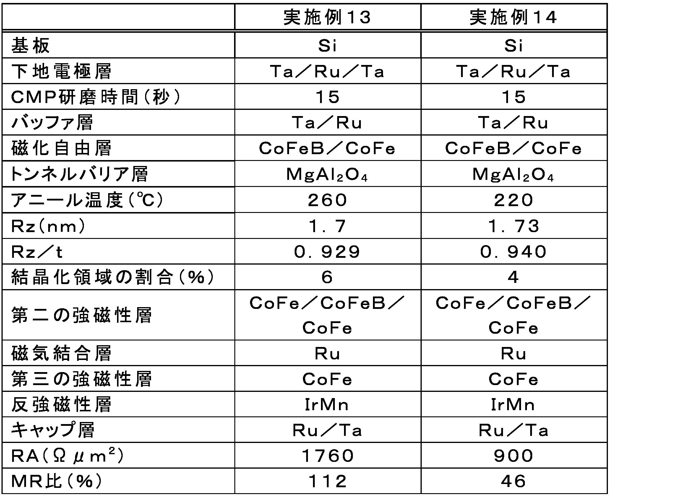
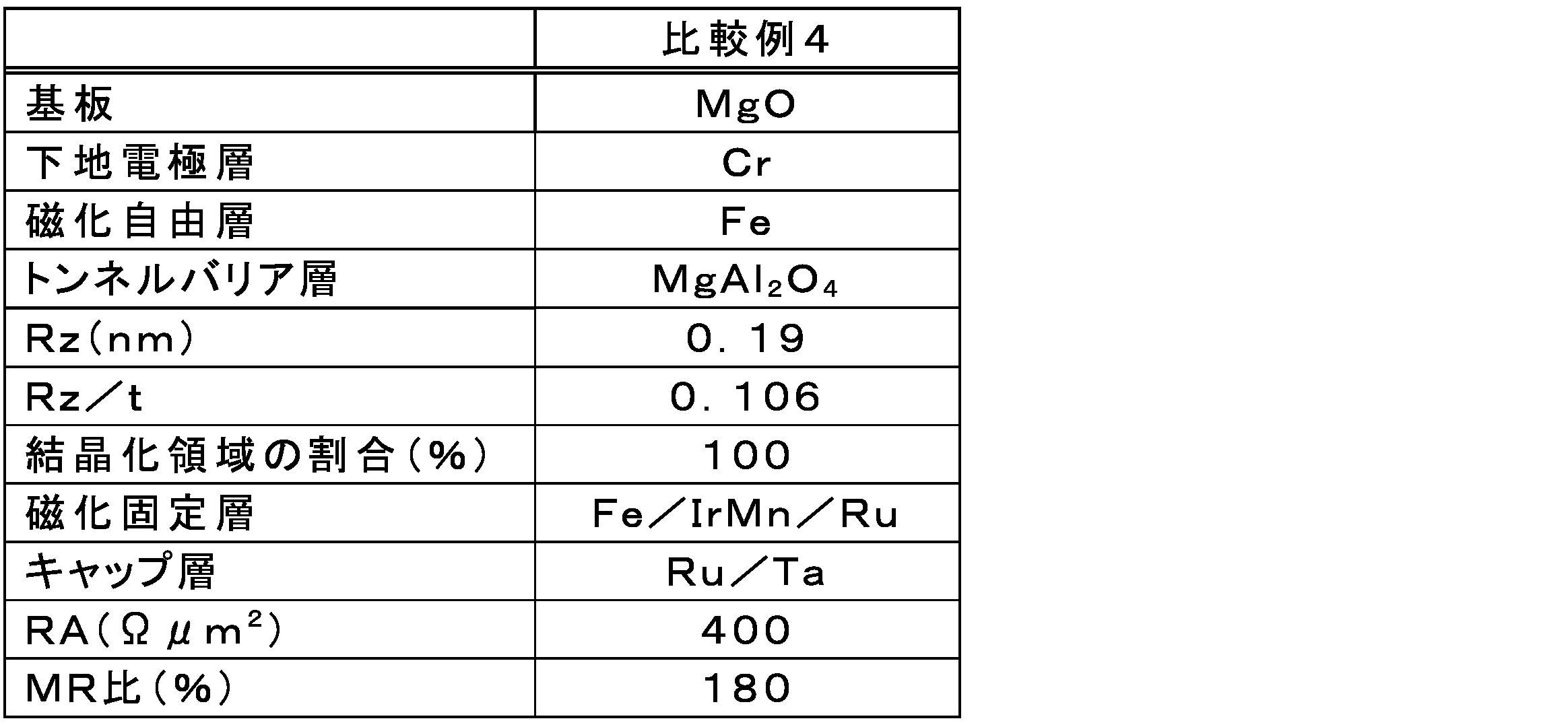
表1~表7に示されるように、実施例1~実施例14のRz/tは、Rz/t<1となっており、比較例1~比較例4のRz/tは、Rz/t>1となっている。実施例1~実施例14は、比較例1~比較例4と比較して、MR比の低減を抑制しつつ、高いRAを有することが示された。また、実施例1~9及び11~13(結晶化領域の割合が5%超かつ65%未満)は、実施例10、14(結晶化領域の割合が5%以下又は65%以上)と比較して、MR比の低減を抑制しつつ、特に高いRAを有することが示された。 As shown in Tables 1 to 7, the Rz/t of Examples 1 to 14 is Rz/t<1, and the Rz/t of Comparative Examples 1 to 4 is Rz/t>1. Compared with Comparative Examples 1 to 4, Examples 1 to 14 were shown to have high RA while suppressing the decrease in MR ratio. Also, Examples 1 to 9 and 11 to 13 (proportion of crystallized region is more than 5% and less than 65%) were shown to have particularly high RA while suppressing the decrease in MR ratio, compared with Examples 10 and 14 (proportion of crystallized region is 5% or less or 65% or more).
本実施形態によれば、MR比の低減を抑制しつつ、高いRAを有する磁気抵抗効果素子、及びそのような磁気抵抗効果素子を製造する方法が提供される。
以上説明したように、本発明の一態様に係る磁気抵抗効果素子では、トンネルバリア層は、式(1)で表されるスピネル構造を有する酸化物材料を含んでもよい。
A1-xBxOy …(1)
式(1)中、Aは、Mg、Zn、Cu、Cd、Li、Ni、Co、Fe、Mn、Cr、Hg、及びVからなる群より選択される少なくとも一種の元素を表し、Bは、Al、Ga、In、Sc、Ti、V、Cr、Mn、Fe、Rh、Ir、Ge、及びCoからなる群より選択される少なくとも一種の元素を表し、0<x≦1、及び、0.35≦y≦1.7である。
本発明の一態様に係る磁気抵抗効果素子を作製する方法は、第一の強磁性層を形成する工程と、第一の強磁性層上にMgAl合金層を形成する工程と、MgAl合金層を酸化して、少なくとも一つのアモルファス領域と、Mg1-xAlxOy(0<x≦1、0.35≦y≦1.7)で表されるスピネル構造からなる少なくとも一つの結晶化領域とを含むトンネルバリア層を形成する工程と、トンネルバリア層上に第二の強磁性層を形成する工程と、を備え、トンネルバリア層は、上面と、当該上面の反対側に位置する下面とを有し、トンネルバリア層の上面の最大高さ粗さ及び下面の最大高さ粗さのうち、より大きな最大高さ粗さをRzとし、トンネルバリア層の厚さをtとしたとき、Rz/t<1である。
According to the present embodiment, a magnetoresistive element having a high RA while suppressing a decrease in the MR ratio, and a method for manufacturing such a magnetoresistive element are provided.
As described above, in the magnetoresistive element according to one aspect of the present invention, the tunnel barrier layer may contain an oxide material having a spinel structure represented by formula (1).
A 1-x B x O y ... (1)
In formula (1), A represents at least one element selected from the group consisting of Mg, Zn, Cu, Cd, Li, Ni, Co, Fe, Mn, Cr, Hg, and V, and B represents at least one element selected from the group consisting of Al, Ga, In, Sc, Ti, V, Cr, Mn, Fe, Rh, Ir, Ge, and Co, where 0<x≦1 and 0.35≦y≦1.7.
A method for producing a magnetoresistance effect element according to one embodiment of the present invention includes the steps of forming a first ferromagnetic layer, forming an MgAl alloy layer on the first ferromagnetic layer, oxidizing the MgAl alloy layer to form a tunnel barrier layer including at least one amorphous region and at least one crystallized region having a spinel structure represented by Mg1 - xAlxOy ( 0<x≦1, 0.35≦y≦1.7), and forming a second ferromagnetic layer on the tunnel barrier layer, wherein the tunnel barrier layer has an upper surface and a lower surface located opposite to the upper surface, and Rz/t<1 is satisfied, where Rz is the larger of the maximum roughness in height of the upper surface and the maximum roughness in height of the lower surface of the tunnel barrier layer, and t is a thickness of the tunnel barrier layer.
1…磁気抵抗効果素子、31…第一の強磁性層、32…第二の強磁性層、33…トンネルバリア層、33a…上面、33b…下面、61…アモルファス領域、62…結晶化領域。 1...magnetoresistance effect element, 31...first ferromagnetic layer, 32...second ferromagnetic layer, 33...tunnel barrier layer, 33a...upper surface, 33b...lower surface, 61...amorphous region, 62...crystallized region.
Claims (14)
第二の強磁性層と、
前記第一の強磁性層と前記第二の強磁性層との間に積層されたトンネルバリア層と、
を備え、
前記トンネルバリア層は、上面と、当該上面の反対側に位置する下面とを有し、
前記トンネルバリア層の前記上面の最大高さ粗さ及び前記下面の最大高さ粗さのうち、より大きな最大高さ粗さをRzとし、前記トンネルバリア層の厚さをtとしたとき、Rz/t<1であり、
前記トンネルバリア層は、少なくとも一つのアモルファス領域と、式(1)で表される組成を有する少なくとも一つの結晶化領域とを含む、磁気抵抗効果素子。
A1-xBxOy …(1)
[式中、Aは、Mg、Zn、Cu、Cd、Li、Ni、Co、Fe、Mn、Cr、Hg、及びVからなる群より選択される少なくとも一種の元素を表し、Bは、Al、Ga、In、Sc、Cr、Rh、Ir、Ge、及びCoからなる群より選択される少なくとも一種の元素を表し、0<x≦1、及び、0.35≦y≦1.7である。] a first ferromagnetic layer;
a second ferromagnetic layer; and
a tunnel barrier layer stacked between the first ferromagnetic layer and the second ferromagnetic layer;
Equipped with
the tunnel barrier layer has an upper surface and a lower surface opposite the upper surface;
Rz is a larger maximum roughness in maximum height of the upper surface and the lower surface of the tunnel barrier layer, and t is a thickness of the tunnel barrier layer, Rz/t<1;
A magnetoresistance effect element, wherein the tunnel barrier layer includes at least one amorphous region and at least one crystallized region having a composition represented by formula (1).
A 1-x B x O y ... (1)
[In the formula, A represents at least one element selected from the group consisting of Mg, Zn, Cu, Cd, Li, Ni, Co, Fe, Mn, Cr, Hg, and V, and B represents at least one element selected from the group consisting of Al, Ga, In, Sc , Cr , Rh, Ir, Ge, and Co, and 0<x≦1 and 0.35≦y≦1.7.]
第二の強磁性層と、
前記第一の強磁性層と前記第二の強磁性層との間に積層されたトンネルバリア層と、
を備え、
前記トンネルバリア層は、上面と、当該上面の反対側に位置する下面とを有し、
前記トンネルバリア層の前記上面の最大高さ粗さ及び前記下面の最大高さ粗さのうち、より大きな最大高さ粗さをRzとし、前記トンネルバリア層の厚さをtとしたとき、Rz/t<1であり、
前記トンネルバリア層は、少なくとも一つのアモルファス領域と、式(1)で表される組成を有する少なくとも一つの結晶化領域とを含み、前記少なくとも一つのアモルファス領域と、前記少なくとも一つの結晶化領域とは、積層方向に並ぶ、磁気抵抗効果素子。
A1-xBxOy …(1)
[式中、Aは、Mg、Zn、Cu、Cd、Li、Ni、Co、Fe、Mn、Cr、Hg、及びVからなる群より選択される少なくとも一種の元素を表し、Bは、Al、Ga、In、Sc、Ti、Cr、Rh、Ir、Ge、及びCoからなる群より選択される少なくとも一種の元素を表し、0<x≦1、及び、0.35≦y≦1.7である。] a first ferromagnetic layer;
a second ferromagnetic layer; and
a tunnel barrier layer stacked between the first ferromagnetic layer and the second ferromagnetic layer;
Equipped with
the tunnel barrier layer has an upper surface and a lower surface opposite the upper surface;
Rz is a larger maximum roughness in maximum height of the upper surface and the lower surface of the tunnel barrier layer, and t is a thickness of the tunnel barrier layer, Rz/t<1;
A magnetoresistive effect element, wherein the tunnel barrier layer includes at least one amorphous region and at least one crystallized region having a composition represented by formula (1), and the at least one amorphous region and the at least one crystallized region are aligned in a stacking direction .
A 1-x B x O y ... (1)
[In the formula, A represents at least one element selected from the group consisting of Mg, Zn, Cu, Cd, Li, Ni, Co, Fe, Mn, Cr, Hg, and V, and B represents at least one element selected from the group consisting of Al, Ga, In, Sc, Ti, Cr, Rh, Ir, Ge, and Co, and 0<x≦1 and 0.35≦y≦1.7.]
前記幅の最大値は、8nm未満である、請求項1~5のいずれか1項に記載の磁気抵抗効果素子。 the at least one crystallized region has a width along an in-plane direction of the tunnel barrier layer,
6. The magnetoresistance effect element according to claim 1, wherein the maximum value of the width is less than 8 nm.
前記第一の強磁性層上にMgAl合金層を形成する工程と、
前記MgAl合金層を酸化して、少なくとも一つのアモルファス領域と、Mg1-xAlxOy(0<x≦1、0.35≦y≦1.7)で表される組成を有する少なくとも一つの結晶化領域とを含むトンネルバリア層を形成する工程と、
前記トンネルバリア層上に第二の強磁性層を形成する工程と、
を備え、
前記トンネルバリア層は、上面と、当該上面の反対側に位置する下面とを有し、
前記トンネルバリア層の前記上面の最大高さ粗さ及び前記下面の最大高さ粗さのうち、より大きな最大高さ粗さをRzとし、前記トンネルバリア層の厚さをtとしたとき、Rz/t<1である、磁気抵抗効果素子を製造する方法。 forming a first ferromagnetic layer;
forming an MgAl alloy layer on the first ferromagnetic layer;
oxidizing the MgAl alloy layer to form a tunnel barrier layer including at least one amorphous region and at least one crystallized region having a composition represented by Mg 1-x Al x O y (0<x≦1, 0.35≦y≦1.7);
forming a second ferromagnetic layer on the tunnel barrier layer;
Equipped with
the tunnel barrier layer has an upper surface and a lower surface opposite the upper surface;
A method for manufacturing a magnetoresistive effect element, wherein Rz is the larger of the maximum height roughness of the upper surface and the maximum height roughness of the lower surface of the tunnel barrier layer, and t is a thickness of the tunnel barrier layer, such that Rz/t<1.
14. The method of claim 13 , wherein the step of oxidizing the MgAl alloy layer includes the step of oxidizing the MgAl alloy layer by at least one of radical oxidation, plasma oxidation, ozone oxidation, and natural oxidation.
Priority Applications (2)
| Application Number | Priority Date | Filing Date | Title |
|---|---|---|---|
| JP2022190513A JP7488317B2 (en) | 2019-01-11 | 2022-11-29 | Magnetoresistive element and method for manufacturing the same - Patents.com |
| JP2024076356A JP2024097908A (en) | 2019-01-11 | 2024-05-09 | Magnetoresistive element and method for manufacturing the same - Patents.com |
Applications Claiming Priority (2)
| Application Number | Priority Date | Filing Date | Title |
|---|---|---|---|
| JP2019003789A JP7186622B2 (en) | 2019-01-11 | 2019-01-11 | Magnetoresistive element and method for manufacturing magnetoresistive element |
| JP2022190513A JP7488317B2 (en) | 2019-01-11 | 2022-11-29 | Magnetoresistive element and method for manufacturing the same - Patents.com |
Related Parent Applications (1)
| Application Number | Title | Priority Date | Filing Date |
|---|---|---|---|
| JP2019003789A Division JP7186622B2 (en) | 2019-01-11 | 2019-01-11 | Magnetoresistive element and method for manufacturing magnetoresistive element |
Related Child Applications (1)
| Application Number | Title | Priority Date | Filing Date |
|---|---|---|---|
| JP2024076356A Division JP2024097908A (en) | 2019-01-11 | 2024-05-09 | Magnetoresistive element and method for manufacturing the same - Patents.com |
Publications (2)
| Publication Number | Publication Date |
|---|---|
| JP2023014198A JP2023014198A (en) | 2023-01-26 |
| JP7488317B2 true JP7488317B2 (en) | 2024-05-21 |
Family
ID=71667265
Family Applications (3)
| Application Number | Title | Priority Date | Filing Date |
|---|---|---|---|
| JP2019003789A Active JP7186622B2 (en) | 2019-01-11 | 2019-01-11 | Magnetoresistive element and method for manufacturing magnetoresistive element |
| JP2022190513A Active JP7488317B2 (en) | 2019-01-11 | 2022-11-29 | Magnetoresistive element and method for manufacturing the same - Patents.com |
| JP2024076356A Pending JP2024097908A (en) | 2019-01-11 | 2024-05-09 | Magnetoresistive element and method for manufacturing the same - Patents.com |
Family Applications Before (1)
| Application Number | Title | Priority Date | Filing Date |
|---|---|---|---|
| JP2019003789A Active JP7186622B2 (en) | 2019-01-11 | 2019-01-11 | Magnetoresistive element and method for manufacturing magnetoresistive element |
Family Applications After (1)
| Application Number | Title | Priority Date | Filing Date |
|---|---|---|---|
| JP2024076356A Pending JP2024097908A (en) | 2019-01-11 | 2024-05-09 | Magnetoresistive element and method for manufacturing the same - Patents.com |
Country Status (1)
| Country | Link |
|---|---|
| JP (3) | JP7186622B2 (en) |
Citations (6)
| Publication number | Priority date | Publication date | Assignee | Title |
|---|---|---|---|---|
| WO2003021579A1 (en) | 2001-08-29 | 2003-03-13 | Lambeth David N | Magnetic material structures, devices and methods |
| JP2003218324A (en) | 2002-01-18 | 2003-07-31 | Sony Corp | Magnetic storage device and method of manufacturing the same |
| US20040058196A1 (en) | 2002-08-29 | 2004-03-25 | Lambeth David N | Magnetic material structures, devices and methods |
| JP2007048972A (en) | 2005-08-10 | 2007-02-22 | Tdk Corp | Magnetoresistive element, substrate, wafer, head gimbal assembly, hard disk device, magnetic memory element, magnetic sensor assembly, and method of manufacturing magnetoresistive element |
| US20130221461A1 (en) | 2012-02-27 | 2013-08-29 | National Institute For Materials Science | Ferromagnetic Tunnel Junction Structure and Magnetoresistive Effect Device and Spintronics Device Utilizing Same |
| US20140264673A1 (en) | 2013-03-14 | 2014-09-18 | Kabushiki Kaisha Toshiba | Magnetoresistive element and magnetic memory |
Family Cites Families (7)
| Publication number | Priority date | Publication date | Assignee | Title |
|---|---|---|---|---|
| JP2003283000A (en) * | 2002-03-27 | 2003-10-03 | Toshiba Corp | Magnetoresistive element and magnetic memory having the same |
| JP2008034784A (en) * | 2006-06-30 | 2008-02-14 | Alps Electric Co Ltd | Tunnel-type magnetic detection element and method of manufacturing the same |
| JP2008085243A (en) * | 2006-09-29 | 2008-04-10 | Fujitsu Ltd | Magnetoresistive element and manufacturing method thereof |
| JP5586028B2 (en) * | 2009-04-16 | 2014-09-10 | 独立行政法人物質・材料研究機構 | Ferromagnetic tunnel junction, magnetoresistive effect element and spintronic device using the same |
| EP3413363B1 (en) * | 2016-02-02 | 2021-03-24 | National Institute for Materials Science | Ferromagnetic tunnel junction, magnetoresistive effect element and spintronics device in which said ferromagnetic tunnel junction is used, and method of manufacturing ferromagnetic tunnel junction |
| JP6299897B2 (en) * | 2017-02-13 | 2018-03-28 | Tdk株式会社 | Tunnel layer |
| JP6857421B2 (en) * | 2017-06-14 | 2021-04-14 | 国立研究開発法人物質・材料研究機構 | Ferromagnetic tunnel junction, spintronics device using it, and method for manufacturing ferromagnetic tunnel junction |
-
2019
- 2019-01-11 JP JP2019003789A patent/JP7186622B2/en active Active
-
2022
- 2022-11-29 JP JP2022190513A patent/JP7488317B2/en active Active
-
2024
- 2024-05-09 JP JP2024076356A patent/JP2024097908A/en active Pending
Patent Citations (10)
| Publication number | Priority date | Publication date | Assignee | Title |
|---|---|---|---|---|
| WO2003021579A1 (en) | 2001-08-29 | 2003-03-13 | Lambeth David N | Magnetic material structures, devices and methods |
| JP2005502199A (en) | 2001-08-29 | 2005-01-20 | エヌ ランベス、デイビッド | Magnetic material structure, apparatus using magnetic material structure, and method of forming magnetic material |
| JP2003218324A (en) | 2002-01-18 | 2003-07-31 | Sony Corp | Magnetic storage device and method of manufacturing the same |
| US20040058196A1 (en) | 2002-08-29 | 2004-03-25 | Lambeth David N | Magnetic material structures, devices and methods |
| JP2007048972A (en) | 2005-08-10 | 2007-02-22 | Tdk Corp | Magnetoresistive element, substrate, wafer, head gimbal assembly, hard disk device, magnetic memory element, magnetic sensor assembly, and method of manufacturing magnetoresistive element |
| US20070053114A1 (en) | 2005-08-10 | 2007-03-08 | Tdk Corporation | TMR element having a tunnel barrier which includes crystalline portions and non-crystalline portions |
| US20130221461A1 (en) | 2012-02-27 | 2013-08-29 | National Institute For Materials Science | Ferromagnetic Tunnel Junction Structure and Magnetoresistive Effect Device and Spintronics Device Utilizing Same |
| JP2013175615A (en) | 2012-02-27 | 2013-09-05 | National Institute For Materials Science | Ferromagnetic tunnel junction and magnetoresistance effect element and spintronics device using the same |
| US20140264673A1 (en) | 2013-03-14 | 2014-09-18 | Kabushiki Kaisha Toshiba | Magnetoresistive element and magnetic memory |
| JP2014179428A (en) | 2013-03-14 | 2014-09-25 | Toshiba Corp | Magnetoresistive element and magnetic memory |
Also Published As
| Publication number | Publication date |
|---|---|
| JP2023014198A (en) | 2023-01-26 |
| JP2020113655A (en) | 2020-07-27 |
| JP7186622B2 (en) | 2022-12-09 |
| JP2024097908A (en) | 2024-07-19 |
Similar Documents
| Publication | Publication Date | Title |
|---|---|---|
| CN107408626B (en) | Magnetoresistive effect element | |
| US20100178528A1 (en) | Tunnel magnetoresistive thin film and magnetic multilayer film formation apparatus | |
| CN107887506B (en) | Magnetoresistive effect element | |
| EP2434556A1 (en) | Ferromagnetic tunnel junction structure and magnetoresistive element using same | |
| JP6438636B1 (en) | Magnetoresistive effect element | |
| JP2005116701A (en) | Magnetic detecting element | |
| CN107408625B (en) | Magnetoresistive effect element | |
| US20180294404A1 (en) | Magnetoresistive effect element | |
| JP2018147998A (en) | Magnetoresistance effect element | |
| CN107431124B (en) | Magnetoresistive effect element | |
| US7760473B2 (en) | Magnetoresistance element employing Heusler alloy as magnetic layer | |
| WO2018159624A1 (en) | Ferromagnetic multilayer film, magnetoresistance effect element, and method for manufacturing ferromagnetic multilayer film | |
| JP6480089B2 (en) | Magnetoresistive effect element | |
| US11005035B2 (en) | Magnetoresistive effect element | |
| US20190273203A1 (en) | Magnetoresistive effect element | |
| JP7488317B2 (en) | Magnetoresistive element and method for manufacturing the same - Patents.com | |
| JP2007194327A (en) | Tunnel type magnetic sensor | |
| JP4674498B2 (en) | Magnetic detection element | |
| WO2017110534A1 (en) | Laminate film for current-perpendicular-to-plane giant magnetoresistive element, current-perpendicular-to-plane giant magnetoresistive element, and use therefor | |
| JP3551196B2 (en) | Method of manufacturing magnetoresistive element | |
| JP2018098305A (en) | Laminated film for high-sensitivity surface direct-coupled giant magnetoresistance element, high sensitivity direct-coupled giant magnetoresistance element, and use thereof | |
| WO2018061710A1 (en) | Magnetoresistive effect element | |
| JP2020155434A (en) | Magnetoresistance effect element | |
| JP2020155435A (en) | Magnetoresistance effect element | |
| Li et al. | Electrical and magnetic properties of nano-oxide added spin valves |
Legal Events
| Date | Code | Title | Description |
|---|---|---|---|
| A621 | Written request for application examination |
Free format text: JAPANESE INTERMEDIATE CODE: A621 Effective date: 20221129 |
|
| A977 | Report on retrieval |
Free format text: JAPANESE INTERMEDIATE CODE: A971007 Effective date: 20230929 |
|
| A131 | Notification of reasons for refusal |
Free format text: JAPANESE INTERMEDIATE CODE: A131 Effective date: 20231003 |
|
| A601 | Written request for extension of time |
Free format text: JAPANESE INTERMEDIATE CODE: A601 Effective date: 20231201 |
|
| A521 | Request for written amendment filed |
Free format text: JAPANESE INTERMEDIATE CODE: A523 Effective date: 20240129 |
|
| TRDD | Decision of grant or rejection written | ||
| A01 | Written decision to grant a patent or to grant a registration (utility model) |
Free format text: JAPANESE INTERMEDIATE CODE: A01 Effective date: 20240409 |
|
| A61 | First payment of annual fees (during grant procedure) |
Free format text: JAPANESE INTERMEDIATE CODE: A61 Effective date: 20240509 |
|
| R150 | Certificate of patent or registration of utility model |
Ref document number: 7488317 Country of ref document: JP Free format text: JAPANESE INTERMEDIATE CODE: R150 |