JP7479850B2 - Image Sensor - Google Patents
Image Sensor Download PDFInfo
- Publication number
- JP7479850B2 JP7479850B2 JP2020001233A JP2020001233A JP7479850B2 JP 7479850 B2 JP7479850 B2 JP 7479850B2 JP 2020001233 A JP2020001233 A JP 2020001233A JP 2020001233 A JP2020001233 A JP 2020001233A JP 7479850 B2 JP7479850 B2 JP 7479850B2
- Authority
- JP
- Japan
- Prior art keywords
- region
- semiconductor layer
- pattern
- grid pattern
- light
- Prior art date
- Legal status (The legal status is an assumption and is not a legal conclusion. Google has not performed a legal analysis and makes no representation as to the accuracy of the status listed.)
- Active
Links
- 239000010410 layer Substances 0.000 claims description 212
- 239000004065 semiconductor Substances 0.000 claims description 201
- 238000002955 isolation Methods 0.000 claims description 59
- 238000006243 chemical reaction Methods 0.000 claims description 48
- 239000000463 material Substances 0.000 claims description 16
- 239000007769 metal material Substances 0.000 claims description 11
- 230000000903 blocking effect Effects 0.000 claims description 10
- 229910052751 metal Inorganic materials 0.000 claims description 4
- 239000002184 metal Substances 0.000 claims description 4
- 150000004767 nitrides Chemical class 0.000 claims description 3
- 239000002356 single layer Substances 0.000 claims 1
- 239000011229 interlayer Substances 0.000 description 23
- 238000000034 method Methods 0.000 description 16
- 238000009792 diffusion process Methods 0.000 description 15
- 230000001681 protective effect Effects 0.000 description 14
- 230000003667 anti-reflective effect Effects 0.000 description 13
- 229910052581 Si3N4 Inorganic materials 0.000 description 11
- HQVNEWCFYHHQES-UHFFFAOYSA-N silicon nitride Chemical compound N12[Si]34N5[Si]62N3[Si]51N64 HQVNEWCFYHHQES-UHFFFAOYSA-N 0.000 description 11
- VYPSYNLAJGMNEJ-UHFFFAOYSA-N Silicium dioxide Chemical compound O=[Si]=O VYPSYNLAJGMNEJ-UHFFFAOYSA-N 0.000 description 10
- 229910052814 silicon oxide Inorganic materials 0.000 description 10
- 229910052721 tungsten Inorganic materials 0.000 description 10
- 239000010937 tungsten Substances 0.000 description 10
- 238000005530 etching Methods 0.000 description 9
- WFKWXMTUELFFGS-UHFFFAOYSA-N tungsten Chemical compound [W] WFKWXMTUELFFGS-UHFFFAOYSA-N 0.000 description 9
- XUIMIQQOPSSXEZ-UHFFFAOYSA-N Silicon Chemical compound [Si] XUIMIQQOPSSXEZ-UHFFFAOYSA-N 0.000 description 8
- XLOMVQKBTHCTTD-UHFFFAOYSA-N Zinc monoxide Chemical compound [Zn]=O XLOMVQKBTHCTTD-UHFFFAOYSA-N 0.000 description 8
- 239000010949 copper Substances 0.000 description 8
- 229910052710 silicon Inorganic materials 0.000 description 8
- 239000010703 silicon Substances 0.000 description 8
- RYGMFSIKBFXOCR-UHFFFAOYSA-N Copper Chemical compound [Cu] RYGMFSIKBFXOCR-UHFFFAOYSA-N 0.000 description 6
- 239000004020 conductor Substances 0.000 description 6
- 229910052802 copper Inorganic materials 0.000 description 6
- 230000002596 correlated effect Effects 0.000 description 6
- 238000010586 diagram Methods 0.000 description 6
- 230000000875 corresponding effect Effects 0.000 description 5
- 230000005611 electricity Effects 0.000 description 5
- 238000004519 manufacturing process Methods 0.000 description 5
- 230000003068 static effect Effects 0.000 description 5
- 229910052782 aluminium Inorganic materials 0.000 description 4
- XAGFODPZIPBFFR-UHFFFAOYSA-N aluminium Chemical compound [Al] XAGFODPZIPBFFR-UHFFFAOYSA-N 0.000 description 4
- 239000011810 insulating material Substances 0.000 description 4
- 125000006850 spacer group Chemical group 0.000 description 4
- 239000010936 titanium Substances 0.000 description 4
- 239000011787 zinc oxide Substances 0.000 description 4
- NRTOMJZYCJJWKI-UHFFFAOYSA-N Titanium nitride Chemical compound [Ti]#N NRTOMJZYCJJWKI-UHFFFAOYSA-N 0.000 description 3
- 238000007599 discharging Methods 0.000 description 3
- 239000012535 impurity Substances 0.000 description 3
- 229910017090 AlO 2 Inorganic materials 0.000 description 2
- RTAQQCXQSZGOHL-UHFFFAOYSA-N Titanium Chemical compound [Ti] RTAQQCXQSZGOHL-UHFFFAOYSA-N 0.000 description 2
- 238000004380 ashing Methods 0.000 description 2
- 150000001875 compounds Chemical class 0.000 description 2
- 238000001312 dry etching Methods 0.000 description 2
- 229910000449 hafnium oxide Inorganic materials 0.000 description 2
- WIHZLLGSGQNAGK-UHFFFAOYSA-N hafnium(4+);oxygen(2-) Chemical compound [O-2].[O-2].[Hf+4] WIHZLLGSGQNAGK-UHFFFAOYSA-N 0.000 description 2
- AMGQUBHHOARCQH-UHFFFAOYSA-N indium;oxotin Chemical compound [In].[Sn]=O AMGQUBHHOARCQH-UHFFFAOYSA-N 0.000 description 2
- 230000031700 light absorption Effects 0.000 description 2
- TWNQGVIAIRXVLR-UHFFFAOYSA-N oxo(oxoalumanyloxy)alumane Chemical compound O=[Al]O[Al]=O TWNQGVIAIRXVLR-UHFFFAOYSA-N 0.000 description 2
- 238000000059 patterning Methods 0.000 description 2
- 230000000149 penetrating effect Effects 0.000 description 2
- 229920002120 photoresistant polymer Polymers 0.000 description 2
- 229910021420 polycrystalline silicon Inorganic materials 0.000 description 2
- 229920005591 polysilicon Polymers 0.000 description 2
- 229910052719 titanium Inorganic materials 0.000 description 2
- YVTHLONGBIQYBO-UHFFFAOYSA-N zinc indium(3+) oxygen(2-) Chemical compound [O--].[Zn++].[In+3] YVTHLONGBIQYBO-UHFFFAOYSA-N 0.000 description 2
- 229910000577 Silicon-germanium Inorganic materials 0.000 description 1
- LEVVHYCKPQWKOP-UHFFFAOYSA-N [Si].[Ge] Chemical compound [Si].[Ge] LEVVHYCKPQWKOP-UHFFFAOYSA-N 0.000 description 1
- 150000004770 chalcogenides Chemical class 0.000 description 1
- 230000000295 complement effect Effects 0.000 description 1
- 238000005516 engineering process Methods 0.000 description 1
- 229910052732 germanium Inorganic materials 0.000 description 1
- GNPVGFCGXDBREM-UHFFFAOYSA-N germanium atom Chemical compound [Ge] GNPVGFCGXDBREM-UHFFFAOYSA-N 0.000 description 1
- 239000012212 insulator Substances 0.000 description 1
- 238000005468 ion implantation Methods 0.000 description 1
- 239000011159 matrix material Substances 0.000 description 1
- 229910044991 metal oxide Inorganic materials 0.000 description 1
- 150000004706 metal oxides Chemical class 0.000 description 1
- 230000003287 optical effect Effects 0.000 description 1
- 239000011368 organic material Substances 0.000 description 1
- BPUBBGLMJRNUCC-UHFFFAOYSA-N oxygen(2-);tantalum(5+) Chemical compound [O-2].[O-2].[O-2].[O-2].[O-2].[Ta+5].[Ta+5] BPUBBGLMJRNUCC-UHFFFAOYSA-N 0.000 description 1
- 230000003071 parasitic effect Effects 0.000 description 1
- 239000002096 quantum dot Substances 0.000 description 1
- MZLGASXMSKOWSE-UHFFFAOYSA-N tantalum nitride Chemical compound [Ta]#N MZLGASXMSKOWSE-UHFFFAOYSA-N 0.000 description 1
- 229910001936 tantalum oxide Inorganic materials 0.000 description 1
- -1 tungsten nitride Chemical class 0.000 description 1
Images


Classifications
-
- H—ELECTRICITY
- H01—ELECTRIC ELEMENTS
- H01L—SEMICONDUCTOR DEVICES NOT COVERED BY CLASS H10
- H01L27/00—Devices consisting of a plurality of semiconductor or other solid-state components formed in or on a common substrate
- H01L27/14—Devices consisting of a plurality of semiconductor or other solid-state components formed in or on a common substrate including semiconductor components sensitive to infrared radiation, light, electromagnetic radiation of shorter wavelength or corpuscular radiation and specially adapted either for the conversion of the energy of such radiation into electrical energy or for the control of electrical energy by such radiation
- H01L27/144—Devices controlled by radiation
- H01L27/146—Imager structures
- H01L27/14601—Structural or functional details thereof
- H01L27/1462—Coatings
- H01L27/14623—Optical shielding
-
- H—ELECTRICITY
- H01—ELECTRIC ELEMENTS
- H01L—SEMICONDUCTOR DEVICES NOT COVERED BY CLASS H10
- H01L27/00—Devices consisting of a plurality of semiconductor or other solid-state components formed in or on a common substrate
- H01L27/14—Devices consisting of a plurality of semiconductor or other solid-state components formed in or on a common substrate including semiconductor components sensitive to infrared radiation, light, electromagnetic radiation of shorter wavelength or corpuscular radiation and specially adapted either for the conversion of the energy of such radiation into electrical energy or for the control of electrical energy by such radiation
- H01L27/144—Devices controlled by radiation
- H01L27/146—Imager structures
- H01L27/14601—Structural or functional details thereof
- H01L27/1462—Coatings
- H01L27/14621—Colour filter arrangements
-
- H—ELECTRICITY
- H01—ELECTRIC ELEMENTS
- H01L—SEMICONDUCTOR DEVICES NOT COVERED BY CLASS H10
- H01L27/00—Devices consisting of a plurality of semiconductor or other solid-state components formed in or on a common substrate
- H01L27/14—Devices consisting of a plurality of semiconductor or other solid-state components formed in or on a common substrate including semiconductor components sensitive to infrared radiation, light, electromagnetic radiation of shorter wavelength or corpuscular radiation and specially adapted either for the conversion of the energy of such radiation into electrical energy or for the control of electrical energy by such radiation
- H01L27/144—Devices controlled by radiation
- H01L27/146—Imager structures
- H01L27/14601—Structural or functional details thereof
- H01L27/1462—Coatings
-
- H—ELECTRICITY
- H01—ELECTRIC ELEMENTS
- H01L—SEMICONDUCTOR DEVICES NOT COVERED BY CLASS H10
- H01L27/00—Devices consisting of a plurality of semiconductor or other solid-state components formed in or on a common substrate
- H01L27/14—Devices consisting of a plurality of semiconductor or other solid-state components formed in or on a common substrate including semiconductor components sensitive to infrared radiation, light, electromagnetic radiation of shorter wavelength or corpuscular radiation and specially adapted either for the conversion of the energy of such radiation into electrical energy or for the control of electrical energy by such radiation
- H01L27/144—Devices controlled by radiation
- H01L27/146—Imager structures
- H01L27/14601—Structural or functional details thereof
- H01L27/14609—Pixel-elements with integrated switching, control, storage or amplification elements
-
- H—ELECTRICITY
- H01—ELECTRIC ELEMENTS
- H01L—SEMICONDUCTOR DEVICES NOT COVERED BY CLASS H10
- H01L27/00—Devices consisting of a plurality of semiconductor or other solid-state components formed in or on a common substrate
- H01L27/14—Devices consisting of a plurality of semiconductor or other solid-state components formed in or on a common substrate including semiconductor components sensitive to infrared radiation, light, electromagnetic radiation of shorter wavelength or corpuscular radiation and specially adapted either for the conversion of the energy of such radiation into electrical energy or for the control of electrical energy by such radiation
- H01L27/144—Devices controlled by radiation
- H01L27/146—Imager structures
- H01L27/14601—Structural or functional details thereof
- H01L27/14625—Optical elements or arrangements associated with the device
- H01L27/14627—Microlenses
-
- H—ELECTRICITY
- H01—ELECTRIC ELEMENTS
- H01L—SEMICONDUCTOR DEVICES NOT COVERED BY CLASS H10
- H01L27/00—Devices consisting of a plurality of semiconductor or other solid-state components formed in or on a common substrate
- H01L27/14—Devices consisting of a plurality of semiconductor or other solid-state components formed in or on a common substrate including semiconductor components sensitive to infrared radiation, light, electromagnetic radiation of shorter wavelength or corpuscular radiation and specially adapted either for the conversion of the energy of such radiation into electrical energy or for the control of electrical energy by such radiation
- H01L27/144—Devices controlled by radiation
- H01L27/146—Imager structures
- H01L27/14601—Structural or functional details thereof
- H01L27/1463—Pixel isolation structures
-
- H—ELECTRICITY
- H01—ELECTRIC ELEMENTS
- H01L—SEMICONDUCTOR DEVICES NOT COVERED BY CLASS H10
- H01L27/00—Devices consisting of a plurality of semiconductor or other solid-state components formed in or on a common substrate
- H01L27/14—Devices consisting of a plurality of semiconductor or other solid-state components formed in or on a common substrate including semiconductor components sensitive to infrared radiation, light, electromagnetic radiation of shorter wavelength or corpuscular radiation and specially adapted either for the conversion of the energy of such radiation into electrical energy or for the control of electrical energy by such radiation
- H01L27/144—Devices controlled by radiation
- H01L27/146—Imager structures
- H01L27/14601—Structural or functional details thereof
- H01L27/14636—Interconnect structures
-
- H—ELECTRICITY
- H01—ELECTRIC ELEMENTS
- H01L—SEMICONDUCTOR DEVICES NOT COVERED BY CLASS H10
- H01L27/00—Devices consisting of a plurality of semiconductor or other solid-state components formed in or on a common substrate
- H01L27/14—Devices consisting of a plurality of semiconductor or other solid-state components formed in or on a common substrate including semiconductor components sensitive to infrared radiation, light, electromagnetic radiation of shorter wavelength or corpuscular radiation and specially adapted either for the conversion of the energy of such radiation into electrical energy or for the control of electrical energy by such radiation
- H01L27/144—Devices controlled by radiation
- H01L27/146—Imager structures
- H01L27/14601—Structural or functional details thereof
- H01L27/14641—Electronic components shared by two or more pixel-elements, e.g. one amplifier shared by two pixel elements
-
- H—ELECTRICITY
- H01—ELECTRIC ELEMENTS
- H01L—SEMICONDUCTOR DEVICES NOT COVERED BY CLASS H10
- H01L27/00—Devices consisting of a plurality of semiconductor or other solid-state components formed in or on a common substrate
- H01L27/14—Devices consisting of a plurality of semiconductor or other solid-state components formed in or on a common substrate including semiconductor components sensitive to infrared radiation, light, electromagnetic radiation of shorter wavelength or corpuscular radiation and specially adapted either for the conversion of the energy of such radiation into electrical energy or for the control of electrical energy by such radiation
- H01L27/144—Devices controlled by radiation
- H01L27/146—Imager structures
- H01L27/14643—Photodiode arrays; MOS imagers
-
- H—ELECTRICITY
- H01—ELECTRIC ELEMENTS
- H01L—SEMICONDUCTOR DEVICES NOT COVERED BY CLASS H10
- H01L27/00—Devices consisting of a plurality of semiconductor or other solid-state components formed in or on a common substrate
- H01L27/14—Devices consisting of a plurality of semiconductor or other solid-state components formed in or on a common substrate including semiconductor components sensitive to infrared radiation, light, electromagnetic radiation of shorter wavelength or corpuscular radiation and specially adapted either for the conversion of the energy of such radiation into electrical energy or for the control of electrical energy by such radiation
- H01L27/144—Devices controlled by radiation
- H01L27/146—Imager structures
- H01L27/14683—Processes or apparatus peculiar to the manufacture or treatment of these devices or parts thereof
- H01L27/14685—Process for coatings or optical elements
-
- H—ELECTRICITY
- H01—ELECTRIC ELEMENTS
- H01L—SEMICONDUCTOR DEVICES NOT COVERED BY CLASS H10
- H01L27/00—Devices consisting of a plurality of semiconductor or other solid-state components formed in or on a common substrate
- H01L27/14—Devices consisting of a plurality of semiconductor or other solid-state components formed in or on a common substrate including semiconductor components sensitive to infrared radiation, light, electromagnetic radiation of shorter wavelength or corpuscular radiation and specially adapted either for the conversion of the energy of such radiation into electrical energy or for the control of electrical energy by such radiation
- H01L27/144—Devices controlled by radiation
- H01L27/146—Imager structures
- H01L27/14601—Structural or functional details thereof
- H01L27/14609—Pixel-elements with integrated switching, control, storage or amplification elements
- H01L27/14612—Pixel-elements with integrated switching, control, storage or amplification elements involving a transistor
Landscapes
- Physics & Mathematics (AREA)
- Engineering & Computer Science (AREA)
- Power Engineering (AREA)
- Electromagnetism (AREA)
- Condensed Matter Physics & Semiconductors (AREA)
- General Physics & Mathematics (AREA)
- Computer Hardware Design (AREA)
- Microelectronics & Electronic Packaging (AREA)
- Solid State Image Pick-Up Elements (AREA)
- Transforming Light Signals Into Electric Signals (AREA)
Description
本発明は、イメージセンサーに関し、より詳しくはイメージ特性がより改善されたイメージセンサーに関する。 The present invention relates to an image sensor, and more particularly to an image sensor with improved image characteristics.
イメージセンサーは、光学イメージ(optical image)を電気信号に変換する半導体素子である。イメージセンサーは、CCD(charge coupled device)型及びCMOS(complementary metal oxide semiconductor)型に分類される。CMOS型イメージセンサーはCIS(CMOS image sensor)と略称される。CISは2次元的に配列された複数のピクセルを具備する。ピクセルの各々はフォトダイオード(photo diode、PD)を含む。フォトダイオードは入射された光を電気信号に変換する役割を果たす。 An image sensor is a semiconductor device that converts an optical image into an electrical signal. Image sensors are classified into charge coupled device (CCD) type and complementary metal oxide semiconductor (CMOS) type. CMOS type image sensors are abbreviated as CIS (CMOS image sensor). A CIS has a number of pixels arranged two-dimensionally. Each pixel includes a photodiode (PD). The photodiode serves to convert incident light into an electrical signal.
本発明は、上記従来技術に鑑みてなされたものであって、本発明の目的は、イメージ特性がより改善されたイメージセンサーを提供することにある。 The present invention has been made in consideration of the above-mentioned conventional technology, and an object of the present invention is to provide an image sensor with improved image characteristics.
上記目的を達成するためになされた本発明の一態様によるイメージセンサーは、第1領域及び第2領域を含み、互いに対向する第1面及び第2面を有する半導体層と、前記半導体層内に配置されて、ピクセルを定義する素子分離膜と、前記半導体層の前記第1領域の前記第1面上に配置された第1グリッドパターンと、前記半導体層の前記第2領域の前記第1面上に配置された遮光パターンと、を含み、前記半導体層の前記第1面から前記第1グリッドパターンの上面は、前記半導体層の前記第1面から前記遮光パターンの上面よりも低いレベルに位置することを特徴とする。 An image sensor according to one aspect of the present invention made to achieve the above object includes a semiconductor layer including a first region and a second region and having a first surface and a second surface facing each other, an isolation film disposed in the semiconductor layer to define pixels, a first grid pattern disposed on the first surface of the first region of the semiconductor layer, and a light-shielding pattern disposed on the first surface of the second region of the semiconductor layer, and is characterized in that an upper surface of the first grid pattern from the first surface of the semiconductor layer is located at a lower level than an upper surface of the light-shielding pattern from the first surface of the semiconductor layer.
上記目的を達成するためになされた本発明の他の態様によるイメージセンサーは、第1領域及び前記第1領域周辺の第2領域を含む半導体層と、前記半導体層内に配置されて、ピクセルを定義する素子分離膜と、前記半導体層の前記第1領域上で前記素子分離膜に沿って延長され、第1パターンを含むグリッドパターンと、前記半導体層の前記第2領域上の遮光パターンと、を含み、前記第1パターンの厚さは前記遮光パターンの厚さよりも小さく、前記第1パターンは、前記遮光パターンの側面を覆うことを特徴とする。 An image sensor according to another aspect of the present invention made to achieve the above object includes a semiconductor layer including a first region and a second region around the first region, an isolation film disposed in the semiconductor layer to define pixels, a grid pattern extending along the isolation film on the first region of the semiconductor layer and including a first pattern, and a light-shielding pattern on the second region of the semiconductor layer, the thickness of the first pattern being smaller than the thickness of the light-shielding pattern, and the first pattern covering a side surface of the light-shielding pattern.
上記目的を達成するためになされた本発明のさらに他の態様によるイメージセンサーは、第1領域及び第2領域を含む半導体層と、前記半導体層内に配置されて、ピクセルを定義する素子分離膜と、前記半導体層の前記第1領域上のグリッドパターンと、前記半導体層の前記第2領域の上の遮光構造体と、を含み、前記グリッドパターンの厚さは、前記遮光構造体の厚さよりも薄いことを特徴とする。 An image sensor according to yet another aspect of the present invention, which has been made to achieve the above object, includes a semiconductor layer including a first region and a second region, an isolation film disposed in the semiconductor layer to define pixels, a grid pattern on the first region of the semiconductor layer, and a light-shielding structure on the second region of the semiconductor layer, and is characterized in that the thickness of the grid pattern is thinner than the thickness of the light-shielding structure.
本発明によれば、グリッドパターンが遮光パターンの積層構造とは異なる積層構造を有するように形成される。グリッドパターンの第1パターンは金属物質を含むが、遮光パターンよりも薄く形成されることによって、静電気を外部へ放出させる通路の役割を果たしながら、光の吸収を最小化させることができる。グリッドパターンの第2パターンは、低屈折物質で形成され、カラーフィルターの縁に隣接して、入射される光を屈折させて該当ピクセルに入射させることができる。したがって、クロストーク(crosstalk)が減少され、光効率が増大されたイメージセンサーを提供することができる。 According to the present invention, the grid pattern is formed to have a layered structure different from that of the light-shielding pattern. The first pattern of the grid pattern includes a metal material and is formed thinner than the light-shielding pattern, thereby minimizing light absorption while acting as a passage for discharging static electricity to the outside. The second pattern of the grid pattern is formed of a low-refractive material and is adjacent to the edge of the color filter, allowing incident light to be refracted and incident on the corresponding pixel. Therefore, an image sensor with reduced crosstalk and increased light efficiency can be provided.
図1は、本発明の一実施形態によるイメージセンサーのブロック図である。 Figure 1 is a block diagram of an image sensor according to one embodiment of the present invention.
図2は、本発明の一実施形態によるイメージセンサーのセンサーアレイの簡略な回路図である。 Figure 2 is a simplified circuit diagram of a sensor array of an image sensor according to one embodiment of the present invention.
図1を参照すると、本発明の一実施形態によるイメージセンサーは、アクティブピクセルセンサーアレイ(Active Pixel Sensor(APS) Array)10、行デコーダー(row decoder)20、行ドライバー(row driver)30、列デコーダー(column decoder)40、タイミング発生器(timing generator)50、相関二重サンプラー(CDS:Correlated Double Sampler)60、アナログデジタルコンバーター(ADC:Analog to Digital Converter)70、及び入出力バッファ(I/O buffer)80を含む。
Referring to FIG. 1, an image sensor according to an embodiment of the present invention includes an Active Pixel Sensor Array (APS) 10, a
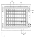
APSアレイ10は、図2に示すように、光が入射される第1領域2及び光が入射されない第2領域4を含み、ピクセル(PX1、PX2)が2次元的に配列される。第1領域2及び第2領域4の各々は、第1ピクセルPX1及び第2ピクセルPX2を含む。第1領域2内に提供された第1ピクセルPX1は、入射光を電気的信号に変換する。第2領域4内に提供された第2ピクセルPX2は、光が入射されないピクセルで発生される電気的信号を出力する。また、第1領域2及び第2領域4内での第1ピクセルPX1及び第2ピクセルPX2は、行ドライバー30から提供された行選択信号(Row SEL)、リセット信号Rx、及び電荷伝送信号Txのような複数の駆動信号によって駆動される。また、APSアレイ10で生成された電気的信号は相関二重サンプラー60に提供される。
2, the
行ドライバー30は、行デコーダー20でデコーディングされた結果に応じて複数のピクセルを駆動するための複数の駆動信号をAPSアレイ10に提供する。ピクセルが行列形状に配列された場合には、駆動信号が各行別に単位ピクセルに提供される。
The
タイミング発生器50は、行デコーダー20及び列デコーダー40にタイミング(timing)信号及び制御信号を提供する。
The
相関二重サンプラー60は、APSアレイ10で生成された電気的信号を受信して維持(hold)及びサンプリングする。相関二重サンプラー60は、特定の雑音レベル(noise level)と電気的信号による信号レベルを二重にサンプリングして、雑音レベルと信号レベルの差に該当する差レベルを出力する。
The correlated
アナログデジタルコンバーター70は、相関二重サンプラー60から出力された差レベルに該当するアナログ信号をデジタル信号に変換して出力する。
The analog-to-
入出力バッファ80は、デジタル信号をラッチ(latch)し、ラッチされた信号は列デコーダー40でのデコーディング結果に応じて順次的に映像信号処理部(未図示)にデジタル信号を出力する。
The input/
図3は、本発明の一実施形態によるイメージセンサーのピクセルを示す回路図である。 Figure 3 is a circuit diagram showing a pixel of an image sensor according to one embodiment of the present invention.
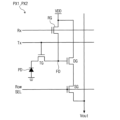
図3を参照すると、第1ピクセルPX1及び第2ピクセルPX2は、入射光を電気的信号に変換する光電変換素子PD及び光電変換素子PDで生成された電気的信号を読み出す読出し素子を各々含む。読出し素子(トランジスタ)は、トランスファーゲートTG、リセット(reset)素子RG、ドライブ(drive)素子DG、又は選択(select)素子SG等を含む。また、トランスファーゲートTGの駆動信号Tx、リセット素子RGの駆動信号Rx、及び選択素子SGの行選択信号Row SELは、同一の行に含まれたピクセルに共通に連結される。以下、単一の光電変換素子PDに対して説明する。 Referring to FIG. 3, the first pixel PX1 and the second pixel PX2 each include a photoelectric conversion element PD that converts incident light into an electrical signal, and a read element that reads out the electrical signal generated by the photoelectric conversion element PD. The read element (transistor) includes a transfer gate TG, a reset element RG, a drive element DG, or a select element SG. In addition, the drive signal Tx of the transfer gate TG, the drive signal Rx of the reset element RG, and the row selection signal Row SEL of the select element SG are commonly connected to pixels included in the same row. Below, a single photoelectric conversion element PD will be described.
より詳細に説明すると、光電変換素子PDは、入射光に対応する電荷を生成及び蓄積する。例えば、光電変換素子PDは、フォトダイオード(photo diode)、フォト素子(photo transistor)、フォトゲート(photo gate)、ピンドフォトダイオード(PPD:Pinned Photo Diode)、及びこれらの組み合わせを含む。光電変換素子PDは、蓄積された電荷を浮遊拡散領域(FD:Floating Diffusion region)に伝達するトランスファーゲートTGに連結される。 More specifically, the photoelectric conversion element PD generates and accumulates electric charges corresponding to incident light. For example, the photoelectric conversion element PD includes a photodiode, a photo transistor, a photogate, a pinned photodiode (PPD), and combinations thereof. The photoelectric conversion element PD is connected to a transfer gate TG that transfers the accumulated electric charges to a floating diffusion region (FD).
浮遊拡散領域FDは、光電変換素子PDから、蓄積された電荷を受信する。浮遊拡散領域FDは寄生キャパシタンスを有するので、電荷が累積的に格納される。また、浮遊拡散領域FDはドライブ素子DGと電気的に連結されているので、ドライブ素子DGを制御する。 The floating diffusion region FD receives the accumulated charge from the photoelectric conversion element PD. Since the floating diffusion region FD has a parasitic capacitance, the charge is stored cumulatively. In addition, the floating diffusion region FD is electrically connected to the drive element DG, and therefore controls the drive element DG.
トランスファーゲートTGは、光電変換素子PDから浮遊拡散領域FDに電荷を伝送する。トランスファーゲートTGは一般的に1つの素子からなり、電荷伝送信号Txによって制御される。 The transfer gate TG transfers electric charge from the photoelectric conversion element PD to the floating diffusion region FD. The transfer gate TG generally consists of one element and is controlled by a charge transfer signal Tx.
リセット素子RGは、浮遊拡散領域FDを定期的にリセットさせ、リセット信号Rxによって制御される。そして、リセット素子RGのソースは浮遊拡散領域FDに連結され、ドレーンは電源電圧VDDに連結される。したがって、リセット信号Rxによってリセット素子RGがターンオンされると、リセット素子RGのドレーンに連結された電源電圧VDDが浮遊拡散領域FDに伝達される。 The reset element RG periodically resets the floating diffusion region FD and is controlled by a reset signal Rx. The source of the reset element RG is connected to the floating diffusion region FD and the drain is connected to the power supply voltage VDD. Therefore, when the reset element RG is turned on by the reset signal Rx, the power supply voltage VDD connected to the drain of the reset element RG is transmitted to the floating diffusion region FD.
ドライブ素子DGは、定電流源(図示せず)と組み合わされてソースフォロワバッファ増幅器(source follower buffer amplifier)の役割を果たし、光電変換素子PDに蓄積された光電荷を受信した浮遊拡散領域FDの電気的ポテンシャルの変化を増幅し、これを出力ラインVoutに出力する。 The drive element DG, in combination with a constant current source (not shown), acts as a source follower buffer amplifier, amplifying the change in electrical potential of the floating diffusion region FD that receives the photocharge stored in the photoelectric conversion element PD, and outputs this to the output line Vout.
選択素子SGは、行単位に読み出すピクセルを選択する役割を果たす。選択素子SGは行選択信号(Row SEL)によって駆動され、選択素子SGがターンオンされると、選択素子SGのドレーンに連結された電源電圧VDDがドライブ素子DGのドレーンに伝達される。 The selection element SG serves to select the pixels to be read out row by row. The selection element SG is driven by a row selection signal (Row SEL), and when the selection element SG is turned on, the power supply voltage VDD connected to the drain of the selection element SG is transmitted to the drain of the drive element DG.
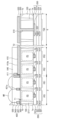
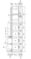
図4は、本発明の一実施形態によるイメージセンサーを示す平面図である。図5は、本発明の一実施形態によるイメージセンサーを示す図であって、図4のI-I’及びII-II’線に沿って切断された断面図である。 Figure 4 is a plan view showing an image sensor according to an embodiment of the present invention. Figure 5 is a cross-sectional view showing an image sensor according to an embodiment of the present invention taken along lines I-I' and II-II' in Figure 4.
図4及び図5を参照すると、半導体層100は、第1領域2、第2領域4、及び第3領域6を含む。第2領域4は半導体層100の第1領域2の周囲に位置し、第3領域6は半導体層100の第2領域4の周囲に位置する。第1領域2は、例えば、受光領域であり、第2領域4は遮光領域であり、第3領域6は入出力領域である。半導体層100は、例えば、シリコン半導体層、ゲルマニウム半導体層、シリコン-ゲルマニウム半導体層、II-VI族化合物半導体層、III-V族化合物半導体層、又はSOI(Silicon on insulator)半導体層である。半導体層100は、第1面1a及び第2面1bを含む。第1面1a及び第2面1bは互いに対向する。
Referring to FIG. 4 and FIG. 5, the
第1素子分離膜DTI1が、半導体層100の第1領域2及び第2領域4内に配置される。第1素子分離膜DTI1は半導体層100を貫通する。例えば、第1素子分離膜DTI1の第1面は、半導体層100の第1面1aと共面を有し、第1素子分離膜DTI1の第1面に対向する第2面は、半導体層100の第2面1bと共面を有する。第1素子分離膜DTI1は、後述する配線構造体200の層間絶縁膜(201、201a)の中で、最下層の層間絶縁膜201aに接触する。第1素子分離膜DTI1は、半導体層100の第1ピクセルPX1及び第2ピクセルPX2を定義する。第1ピクセルPX1は半導体層100の第1領域2内に提供され、第2ピクセルPX2は半導体層100の第2領域4内に提供される。第1素子分離膜DTI1は、例えば、シリコン酸化膜、シリコン窒化膜、誘電膜(例えば、AlO2、HfO2)、半導体物質(例えば、ポリシリコン)、及び金属物質(例えば、タングステン、銅、アルミニウム)の中の少なくとも1つを含む。
The first isolation film DTI1 is disposed in the
保護分離膜SLが、半導体層100の第3領域6内に配置される。保護分離膜SLは半導体層100を貫通する。例えば、保護分離膜SLの第1面は、半導体層100の第1面1aと共面を有し、保護分離膜SLの第1面に対向する第2面は、半導体層100の第2面1bと共面を有する。保護分離膜SLは、後述する配線絶縁膜209に接触する。保護分離膜SLは、半導体層100の第3領域6内で貫通ビア領域TVRを定義する。一例として、保護分離膜SLは多角形又は円形のリング形状を有する。他の実施形態として、保護分離膜SLは多角形又は円形を含むグリッド構造を有する。保護分離膜SLは、シリコン窒化膜、タンタル酸化膜、及びハフニウム酸化膜の中の少なくとも1つを含み得る。
A protective isolation film SL is disposed in the
光電変換素子PDが、半導体層100の第1ピクセルPX1及び第2ピクセルPX2内に配置される。光電変換素子PDは、第1方向X及び第1方向Xと交差する第2方向Yに離隔配置される。半導体層100の第1領域2内に配置された光電変換素子PDは、半導体層100の第2面1bから入射された光を独立的に収集する。光電変換素子PDは、例えば、n型不純物を含み得る。
The photoelectric conversion elements PD are disposed in the first pixel PX1 and the second pixel PX2 of the
配線構造体200が、半導体層100の第1面1a上に配置される。配線構造体200は、層間絶縁膜(201、201a)、第1配線203、第2配線205、ビア207、トランスファーゲートTG、及び配線絶縁膜209を含む。層間絶縁膜(201、201a)は、半導体層100の第1面1a上に順に積層される。層間絶縁膜(201、201a)は、例えば、シリコン酸化膜又はシリコン窒化膜を含む。第1配線203及び第2配線205は、層間絶縁膜(201、201a)内に配置される。例えば、第1配線203は、半導体層100の第1領域2及び第2領域4上に配置される。第2配線205は、半導体層100の第3領域6上に配置される。第2配線205の中で半導体層100に最も隣接する配線205は、配線絶縁膜209上に配置される。第1配線203及び第2配線205は、例えば金属物質(例えば、銅、タングステン)を含む。ビア207は、半導体層100の第3領域6上に配置される。ビア207は、層間絶縁膜(201、201a)内に配置される。ビア207は、第2配線205との間を連結する。図5には図示しないが、ビア207は、半導体層100の第1領域2及び第2領域4上にも配置され得る。ビア207は、例えば金属物質(例えば、銅、タングステン)を含む。
The
トランスファーゲートTGが、半導体層100の第1面1a上に配置される。トランスファーゲートTGは、半導体層100の第1領域2及び第2領域4上に配置される。トランスファーゲートTGは、第1ピクセルPX1及び第2ピクセルPX2の光電変換素子PDに対応するように配置される。トランスファーゲートTGは、半導体層100の第1面1aに最も隣接する最下層の層間絶縁膜201aによって覆われる。配線絶縁膜209は、半導体層100の第3領域6の第1面1aと最下層の層間絶縁膜201aとの間に介在される。配線絶縁膜209は、半導体層100の第3領域6の第1面1aを覆う。配線絶縁膜209は、例えば、シリコン酸化膜、シリコン窒化膜、シリコン酸化窒化膜、又は熱酸化膜を含む。他の実施形態において、配線絶縁膜209は省略され得る。この場合、半導体層100の第1面1aに隣接する第2配線205と半導体層100の第1面1aとの間に層間絶縁膜201が提供される。
The transfer gate TG is disposed on the
反射防止膜300が、半導体層100の第2面1b上に配置される。反射防止膜300は、半導体層100の第1領域~第3領域(2、4、6)上に配置される。半導体層100の第3領域6上に配置された反射防止膜300は、後述するパッド520と半導体層100との間を電気的に絶縁する。反射防止膜300は、例えば、シリコン酸化膜、シリコン窒化膜、シリコン酸化窒化膜、又は高誘電膜(例えば、ハフニウム酸化膜、アルミニウム酸化膜)を含む。
An
グリッドパターン400が、反射防止膜300上に配置される。例えば、グリッドパターン400は、半導体層100の第1領域2の第2面1b上に配置される。グリッドパターン400は、第1素子分離膜DTI1と重畳するように配置され、第1素子分離膜DTI1に沿って延長される。例えば、グリッドパターン400は、第1部分P1及び第2部分P2を含む。第1部分P1は第1方向Xに延長され、第2方向Yに離隔配置される。第2部分P2は第2方向Yに延長され、第1方向Xに離隔配置される。第1部分P1及び第2部分P2は、後述する遮光パターン410に連結される。グリッドパターン400は多角形を含むグリッド構造を有し得る。
The
グリッドパターン400は、半導体層100の第1ピクセルPX1内に配置された光電変換素子PDを露出させる。グリッドパターン400は複数の膜からなる。グリッドパターン400は、反射防止膜300上に順に積層された第1グリッドパターン401(以下では第1パターン401として参照される)及び第2グリッドパターン403(以下では第2パターン403として参照される)を含む。第1パターン401は導電物質を含み得る。例えば、第1パターン401は、金属物質及び金属窒化膜の中の少なくとも1つを含む。第1パターン401は、チタニウム(Ti)、チタニウム窒化物(TiN)、タングステン(W)、アルミニウム(Al)、及び銅(Cu)の中の少なくとも1つを含み得る。第1パターン401は、約100Å~約1500Åの第1厚さT1を有する。第2パターン403は、第1パターン401上に配置される。第2パターン403は、有機物質を含み得る。第2パターン403は、後述するカラーフィルター530の屈折率よりも低い屈折率を有する物質を含む。第2パターン403は、約1.4以下の屈折率を有する低屈折物質を含む。第2パターン403の厚さは、第1パターン401の第1厚さT1よりも大きい。
The
遮光パターン410が、反射防止膜300上に配置される。例えば、遮光パターン410は、半導体層100の第2領域4の第2面1b上に配置される。遮光パターン410は、半導体層100の第2領域4を完全に覆う。例えば、遮光パターン410は、半導体層100の第2ピクセルPX2内に配置された光電変換素子PDを覆う。グリッドパターン400は、遮光パターン410の側面411を覆う。より具体的に、グリッドパターン400の第1パターン401は、遮光パターン410の側面411を覆い、遮光パターン410に接触する。グリッドパターン400は、遮光パターン410の側面411の一部分及び遮光パターン410の側面411に隣接する上面410aの一部分を覆う。即ち、グリッドパターン400は、半導体層100の第1領域2から第2領域4上に延長される。他の実施形態において、グリッドパターン400は、遮光パターン410の側面411の一部分を覆い、遮光パターン410の上面410aを露出させる。
The light-
遮光パターン410は単一膜からなる。遮光パターン410は、約1500Å~約5000Åの第2厚さT2を有する。遮光パターン410の第2厚さT2は、第1パターン401の第1厚さT1よりも厚い(T2>T1)。半導体層100の第2面1bから遮光パターン410の上面410aは、半導体層100の第2面1bから第1パターン401の上面401aよりも高いレベルに位置する。レベルは半導体層100の第2面1bに対して定義される。例えば、第1パターン401の上面と半導体層100の第2面1bとの間の距離は、半導体層100の第2面1bと遮光パターン401の上面410aとの間の距離よりも小さい。遮光パターン410は金属物質(例えば、タングステン(W))を含み得る。
The light-
貫通ビア510が、半導体層100の第3領域6上に配置される。一例として、貫通ビア510の各々は、半導体層100の貫通ビア領域TVR内に配置される。他の実施形態として、複数の貫通ビア510は、半導体層100の貫通ビア領域TVR内に配置される。貫通ビア510は、半導体層100、反射防止膜300、及び配線絶縁膜209を貫通して配線構造体200の第2配線205に連結される。パッド520が、半導体層100の第3領域6上に配置される。例えば、パッド520は、半導体層100の第3領域6の第2面1b上に配置された反射防止膜300上に配置される。パッド520は互いに電気的に絶縁される。パッド520は貫通ビア510上で貫通ビア510に連結される。各貫通ビア510と、各貫通ビア510上の各パッド520とは一体形である。
The through
一実施形態において、パッド520の中の少なくとも1つは、遮光パターン410に連結され得る。図4を参照すると、パッド520の中の少なくとも1つは、遮光パターン410に電気的及び/又は物理的に連結されるように連結パターン521に第1方向Xに沿って連結される。したがって、パッド520の中の少なくとも1つは、遮光パターン410を通じてグリッドパターン400と物理的/電気的に連結される。パッド520の中の少なくとも1つに連結されたグリッドパターン400は、貫通ビア510を通じて第2配線205に連結される。他の実施形態において、パッド520は遮光パターン410及びグリッドパターン400から物理的/電気的に離隔される。この場合、パッド520は遮光パターン410と物理的/電気的に連結されない。グリッドパターン400に連結された遮光パターン410は、半導体層100の第2領域4内に配置された貫通ビア(図示せず)を通じて配線構造体200の第2配線205及び/又は半導体層100の第2領域4内に配置された配線構造体200の第1配線203に電気的に連結され得る。
In one embodiment, at least one of the
グリッドパターン400は、外部から流れ込んだ静電気を外部へ放出する通路の役割を果たす。一実施形態において、静電気は、グリッドパターン400、遮光パターン410、パッド520の中の少なくとも1つ、及びパッド520の中の少なくとも1つに連結された貫通ビア510を通じて第2配線205に放出される。他の実施形態において、静電気は、グリッドパターン400、遮光パターン410、及び貫通ビア(図示せず)を通じて第1配線203及び/又は第2配線205に放出される。この場合、第1配線203及び/又は第2配線205には接地電圧又は負の電圧が印加される。
The
本発明の一実施形態によると、グリッドパターン400は、遮光パターン410の積層構造とは異なる積層構造を有するように形成される。グリッドパターン400の第1パターン401は金属物質を含むが、遮光パターン410よりも薄く形成されることによって、静電気を外部へ放出させる通路の役割を果たしながら、光の吸収を最小化させる。グリッドパターン400の第2パターン403は低屈折物質で形成され、カラーフィルター530の縁に隣接して入射される光を屈折させて該当ピクセルに入射させる。したがって、クロストーク(crosstalk)が減少され、光効率が増大されたイメージセンサーを提供することができる。
According to one embodiment of the present invention, the
カラーフィルター530が、半導体層100の第1領域2上に配置される。例えば、カラーフィルター530は、半導体層100の第2面1b上に配置され、第1ピクセルPX1内に配置された光電変換素子PDに対応するように配置される。カラーフィルター530は、グリッドパターン400及び反射防止膜300を覆う。例えば、カラーフィルター530は、約1.5以上の高屈折率を有する物質を含む。
The
カラーフィルター膜540が、半導体層100の第2領域4上に配置される。例えば、カラーフィルター膜540は、半導体層100の第2面1b上に配置され、第2ピクセルPX2内に配置された光電変換素子PDを覆う。カラーフィルター膜540は反射防止膜300を覆う。パッド520は、カラーフィルター530及びカラーフィルター膜540によって露出される。マイクロレンズMRが、カラーフィルター530上に配置される。マイクロレンズMRは、第1ピクセルPX1内に配置された光電変換素子PDに対応するように配置される。カラーフィルター膜540及びパッド520は、マイクロレンズMRによって露出される。
A
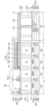
図6は、本発明の一実施形態によるイメージセンサーの他の例を示す図であって、図4のI-I’及びII-II’線に沿って切断した断面図である。 Figure 6 shows another example of an image sensor according to an embodiment of the present invention, and is a cross-sectional view taken along lines I-I' and II-II' in Figure 4.
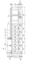
図6を参照すると、遮光構造体410Aが、半導体層100の第2領域4上に配置される。例えば、遮光構造体410Aは、半導体層100の第2領域4の第2面1b上に提供された反射防止膜300上に配置される。遮光構造体410Aは、第2ピクセルPX2内に配置された光電変換素子PDを覆う。遮光構造体410Aは、反射防止膜300上に順に積層された遮光パターン410、第1パターン401、及び第2パターン403を含む。半導体層100の第1領域2上に配置された第1パターン401は、第2領域4上に延長される。第1パターン401は、遮光パターン410の側面411及び上面410aを覆う。第1パターン401は、遮光パターン410に接触及び連結される。半導体層100の第2領域4上で、第1パターン401上に配置された第2パターン403は、第1パターン401に沿って半導体層100の第2領域4上に延長される。第2パターン403は、半導体層100の第2領域4上に配置された第1パターン401の側面及び上面を覆う。一実施形態において、グリッドパターン400の第3厚さT3は、遮光構造体410Aの第4厚さT4よりも小さい(T3<T4)。半導体層100の第2面1bからグリッドパターン400の上面は、半導体層100の第2面1bから遮光構造体410Aの上面よりも低いレベルに位置する。パッド520は、遮光構造体410A、カラーフィルター膜540、及びマイクロレンズMRによって露出される。パッド520の各々の第5厚さT5は、グリッドパターン400の第3厚さT3及び遮光構造体410Aの第4厚さT4よりも小さい(T5<T3、T4)。パッド520の第5厚さT5は、遮光パターン410の第2厚さT2と実質的に同一である。
Referring to FIG. 6, the light-shielding
図7は、本発明の一実施形態によるイメージセンサーのさらに他の例を示す図であって、図4のI-I’及びII-II’線に沿って切断した断面図である。 Figure 7 shows yet another example of an image sensor according to an embodiment of the present invention, and is a cross-sectional view taken along lines I-I' and II-II' in Figure 4.
図7を参照すると、第1素子分離膜DTI1が、半導体層100内で半導体層100の第2面1bから第1面1aに向かって延長される。第1素子分離膜DTI1は、配線構造体200の最下層の層間絶縁膜201aから離隔される。例えば、第1素子分離膜DTI1の第2面は、半導体層100の第2面1bと共面を有し、第1素子分離膜DTI1の第1面は半導体層100の第1面1aと共面を有しない。例えば、第1素子分離膜DTI1の第1面は、半導体層100の第1面1aと第2面1bとの間のレベルに位置する。
Referring to FIG. 7, the first isolation film DTI1 extends from the
図8は、本発明の一実施形態によるイメージセンサーのその他の例を示す図であって、図4のI-I’及びII-II’線に沿って切断した断面図である。 Figure 8 shows another example of an image sensor according to an embodiment of the present invention, and is a cross-sectional view taken along lines I-I' and II-II' in Figure 4.
図8を参照すると、第1光電変換素子PD1及び第2光電変換素子PD2が、第1ピクセルPX1及び第2ピクセルPX2の各々内に配置される。即ち、1つのピクセル内に一対の第1光電変換素子PD1及び第2光電変換素子PD2が配置される。第2素子分離膜DTI2が、第1ピクセルPX1及び第2ピクセルPX2の各々内に配置される。各第2素子分離膜DTI2は、1つのピクセル内に配置された一対の第1光電変換素子PD1と第2光電変換素子PD2との間に配置されて、これらの間を物理的に分離する。一実施形態において、第2素子分離膜DTI2は、第1素子分離膜DTI1に連結される。他の実施形態において、第2素子分離膜DTI2は、第1素子分離膜DTI1から離隔される。第2素子分離膜DTI2は、半導体層100の第2面1bから第1面1aに向かって延長される。第2素子分離膜DTI2は、半導体層100の第2面1bに接触し、第1面1aから離隔される。例えば、第2素子分離膜DTI2の第1面(図8に図示された下面)のレベルは、半導体層100の第1面1aと第2面1bとの間のレベルに位置する。第2素子分離膜DTI2の第2面(図8に図示された上面)は、半導体層100の第2面1bと共面を有する。第2素子分離膜DTI2は、例えば、シリコン酸化膜、シリコン窒化膜、及び誘電膜(AlO2、HfO2)の中の少なくとも1つを含む。
8, the first photoelectric conversion element PD1 and the second photoelectric conversion element PD2 are disposed in each of the first pixel PX1 and the second pixel PX2. That is, a pair of the first photoelectric conversion element PD1 and the second photoelectric conversion element PD2 are disposed in one pixel. The second isolation film DTI2 is disposed in each of the first pixel PX1 and the second pixel PX2. Each second isolation film DTI2 is disposed between the pair of the first photoelectric conversion element PD1 and the second photoelectric conversion element PD2 disposed in one pixel, and physically separates them. In one embodiment, the second isolation film DTI2 is connected to the first isolation film DTI1. In another embodiment, the second isolation film DTI2 is separated from the first isolation film DTI1. The second isolation film DTI2 extends from the
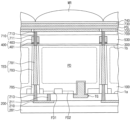
図9は、本発明の他の実施形態によるイメージセンサーを示す断面図である。 Figure 9 is a cross-sectional view showing an image sensor according to another embodiment of the present invention.
図9を参照すると、一対の第1浮遊拡散領域FD1及び第2浮遊拡散領域FD2が、半導体層100内に配置される。一実施形態において、一対の第1浮遊拡散領域FD1及び第2浮遊拡散領域FD2は、半導体層100の第1ピクセルPX1(図5参照)及び第2ピクセルPX2(図5参照)の各々内に配置される。第1浮遊拡散領域FD1及び第2浮遊拡散領域FD2は、半導体層100の第1面1aに隣接するように配置される。第2浮遊拡散領域FD2は、トランスファーゲートTGの一側の半導体層100内に配置される。一実施形態において、図9に示すトランスファーゲートTGの一部は、図5に示すトランスファーゲートTGとは異なり、半導体層100内に埋め込まれる。貫通電極構造体TESが、第1素子分離膜DTI1を貫通する。貫通電極構造体TESは、半導体層100内に配置される。貫通電極構造体TESの各々は、第1ピクセルPX1及び第2ピクセルPX2の各々に対応するように提供される。貫通電極構造体TESの各々は、貫通電極701及び貫通絶縁パターン703を含む。貫通絶縁パターン703は、貫通電極701の側壁を囲む。貫通絶縁パターン703は、例えば、シリコン酸化物、シリコン窒化物、及び/又はシリコン酸窒化物を含む。貫通電極701は、例えば、n型又はp型不純物でドーピングされたポリシリコンを含む。
9, a pair of first and second floating diffusion regions FD1 and FD2 are arranged in the
埋め込み絶縁パターン705が、貫通電極構造体TESの各々と半導体層100の第1面1aとの間に配置される。埋め込み絶縁パターン705の一面は、半導体層100の第1面1a(図9に図示された下面)と共面を有する。埋め込み絶縁パターン705は、例えば、シリコン酸化膜、シリコン窒化膜、シリコン酸化窒化膜の中の少なくとも1つを含む。
The embedded insulating
配線構造体200が、半導体層100の第1面1a上に配置される。配線構造体200は、複数の層間絶縁膜201、連結配線210、第1連結ビア211、及び第2連結ビア213を含む。第1連結ビア211は、層間絶縁膜201の中の少なくとも1つを貫通して第1浮遊拡散領域FD1に連結される。第2連結ビア213は、層間絶縁膜201の中の少なくとも1つ及び埋め込み絶縁パターン705を貫通して貫通電極構造体TESの貫通電極701に連結される。連結配線210は、層間絶縁膜201の中の少なくとも1つ内に配置され、第1連結ビア211と第2連結ビア213との間を連結する。連結配線210、第1連結ビア211、及び第2連結ビア213は、金属物質(例えば、タングステン、銅、アルミニウム)及び金属窒化膜(例えば、タンタル窒化物、チタニウム窒化物、タングステン窒化物)の中の少なくとも1つを含み得る。
The
グリッドパターン400が、半導体層100の第2面1b上に配置される。グリッドパターン400は、第1素子分離膜DTI1及び貫通電極構造体TES上に配置される。グリッドパターン400は、遮光パターン(図5の410参照)に連結される。絶縁膜709が、カラーフィルター530上に配置される。絶縁膜709は、カラーフィルター530の上面を覆う。絶縁膜709は、例えば、シリコン酸化膜、シリコン窒化膜、又はシリコン酸化窒化膜を含む。
A
コンタクトプラグ構造体710が、貫通電極構造体TES上に配置される。コンタクトプラグ構造体710は、反射防止膜300、グリッドパターン400、カラーフィルター530、及び絶縁膜709を貫通する。コンタクトプラグ構造体710は、貫通電極構造体TESに連結される。コンタクトプラグ構造体710の各々は、コンタクトプラグ713及びスペーサー711を含む。コンタクトプラグ713は、反射防止膜300、グリッドパターン400、カラーフィルター530、及び絶縁膜709を貫通する。スペーサー711は、コンタクトプラグ713の側壁を囲む。コンタクトプラグ713は、金属物質(例えば、タングステン)を含む。スペーサー711は、絶縁物質(例えば、シリコン酸化膜、シリコン窒化膜)を含む。
The
下部電極720が、絶縁膜709上に配置される。下部電極720は、光電変換素子PDと対応するように配置される。下部電極720は、互いに離隔して配置される。コンタクトプラグ構造体710の各々は、下部電極720の各々に対応するように配置され、互いに電気的に連結される。下部電極720は、透明導電性物質を含む。例えば、下部電極720は、ITO(IndiumTin Oxide)、IZO(Indium Zinc Oxide)、ZnO(Zinc Oxide)、及び/又は有機透明導電物質を含む。
The
光電変換層PDLが、下部電極720上に配置される。一実施形態において、光電変換層PDLは、有機光電変換層を含む。有機光電変換層は、p型有機半導体物質及びn型有機半導体物質を含み、p型有機半導体物質とn型有機半導体物質とはpn接合を形成する。一例において、光電変換層PDLは、量子ドット(quantum dot)又はカルコゲナイド(chalcogenide)を含む。
The photoelectric conversion layer PDL is disposed on the
上部電極730が、光電変換層PDL上に配置される。上部電極730は、透明導電性物質を含む。例えば、上部電極730は、ITO(Indium Tin Oxide)、IZO(Indium Zinc Oxide)、ZnO(Zinc Oxide)、及び/又は有機透明導電物質を含む。
The
キャッピング層740が、上部電極730上に配置される。キャッピング層740は、絶縁物質を含む。例えば、キャッピング層740は、アルミニウム酸化物、シリコン酸化物、シリコン窒化物、及び/又はシリコン酸窒化物を含む。
A
マイクロレンズMRが、キャッピング層740上に配置される。
The microlens MR is disposed on the
図10は、本発明の他の実施形態によるイメージセンサーを示す平面図である。 Figure 10 is a plan view showing an image sensor according to another embodiment of the present invention.
図10を参照すると、グリッドパターン400は、外側セグメントUP、第1部分P1、及び第2部分P2を含む。外側セグメントUPは、一対の第3部分P3及び一対の第4部分P4を含む。一対の第3部分P3は第2方向Yに延長され、第1方向Xに離隔配置される。一対の第4部分P4は第1方向Xに延長され、第2方向Yに離隔配置される。一対の第3部分P3の端部と一対の第4部分P4の端部とは互いに連結される。したがって、外側セグメントUPは、四角形のリング形状を有する。第1部分P1及び第2部分P2は、外側セグメントUP内に配置される。第1部分P1は、第1方向Xに延長され、第2方向Yに離隔配置される。第2部分P2は、第2方向Yに延長され、第1方向Xに離隔配置される。第1部分P1及び第2部分P2は、外側セグメントUPに連結される。遮光パターン410は、グリッドパターン400の外側セグメントUPの外側壁を囲む。
Referring to FIG. 10, the
図11A~図11Dは、本発明の一実施形態によるイメージセンサーの製造方法を示す図であって、図4のI-I’及びII-II’線に沿って切断した断面図である。 FIGS. 11A to 11D are cross-sectional views taken along lines I-I' and II-II' in FIG. 4, illustrating a method for manufacturing an image sensor according to one embodiment of the present invention.
図11Aを参照すると、半導体層100が提供される。半導体層100は、互いに対向する第1面1a及び第2面1bを含む。半導体層100は、第1領域2、第2領域4、及び第3領域6を含む。光電変換素子PDが、半導体層100の第1領域2及び第2領域4内に形成される。光電変換素子PDは、半導体層100の第1面1aを通じてイオン注入工程を行って形成される。光電変換素子PDは、例えば、n型不純物をドーピングして形成される。
Referring to FIG. 11A, a
配線構造体200が、半導体層100の第1面1a上に形成される。配線構造体200は、トランスファーゲートTG、層間絶縁膜(201、201a)、第1配線203、第2配線205、ビア207、及び配線絶縁膜209を含む。トランスファーゲートTGは、半導体層100の第1領域2及び第2領域4の第1面1a上に形成される。配線絶縁膜209は、半導体層100の第3領域6の第1面1a上に形成される。層間絶縁膜(201、201a)は、半導体層100の第1面1a上に順に形成される。層間絶縁膜(201、201a)の中で最下層の層間絶縁膜201aは、トランスファーゲートTG及び配線絶縁膜209を覆う。第1配線203及び第2配線205が、層間絶縁膜(201、201a)内に配置される。第1配線203は、半導体層100の第1領域2及び第2領域4上に配置される。第2配線205は、半導体層100の第3領域6上に配置される。第1配線203及び第2配線205は、層間絶縁膜(201、201a)によって覆われる。ビア207が、層間絶縁膜(201、201a)内に形成される。ビア207は、半導体層100の第3領域6上に配置される。ビア207は、第2配線205の間を連結する。
The
第1素子分離膜DTI1が、半導体層100の第1領域2及び第2領域4内に形成される。第1素子分離膜DTI1は、半導体層100を蝕刻して第1トレンチTH1を形成し、第1トレンチTH1内に絶縁物質及び/又は導電物質を満たして形成される。一実施形態において、図11Aに示すように、第1トレンチTH1は、半導体層100の第2面1bから蝕刻されて形成される。他の実施形態において、第1トレンチTH1は、配線構造体200を形成する前に、半導体層100の第1面1aから蝕刻されて形成され得る。第1素子分離膜DTI1は、半導体層100の第1領域2及び第2領域4内で半導体層100の第1ピクセルPX1及び第2ピクセルPX2を定義する。第1ピクセルPX1は、半導体層100の第1領域2内に提供され、第2ピクセルPX2は、半導体層100の第2領域4内に提供される。光電変換素子PDが第1ピクセルPX1及び第2ピクセルPX2内に配置される。
A first device isolation film DTI1 is formed in the
図11Bを参照すると、保護分離膜SLが、半導体層100の第3領域6内に形成される。保護分離膜SLは、半導体層100の第3領域6内に第2トレンチTH2を形成し、第2トレンチTH2内に絶縁物質を満たして形成される。一実施形態において、第2トレンチTH2は、半導体層100の第3領域6を貫通して形成される。保護分離膜SLは、半導体層100の第3領域6内で貫通ビア領域TVRを定義する。
Referring to FIG. 11B, a protective isolation film SL is formed in the
反射防止膜300が、半導体層100の第2面1b上に形成される。反射防止膜300は、半導体層100の第2面1b及び半導体層100の第2面1bに露出された第1素子分離膜DTI1の第2面(図11Bに図示された上面)及び保護分離膜SLの第2面(図11Bに図示された上面)を覆う。図11Bに図示しないが、反射防止膜300は、第2トレンチTH2内を満たす。ビアホールVHが、半導体層100の第3領域6内に形成される。例えば、ビアホールVHは、半導体層100の貫通ビア領域TVR内に形成される。ビアホールVHは、反射防止膜300、半導体層100、及び配線絶縁膜209を貫通して第2配線205の中のいずれか1つを露出させる。
An
遮光膜601が、半導体層100の第2面1b上に形成される。遮光膜601は、半導体層100の第1領域~第3領域(2、4、6)上に形成される。遮光膜601は、反射防止膜300の上面を覆い、ビアホールVH内を満たす。遮光膜601は、約1500Å~約5000Åの厚さを有するように形成される。遮光膜601は、金属物質(例えば、タングステン(W))を含み得る。第1マスクパターン603が、遮光膜601上に形成される。第1マスクパターン603は、半導体層100の第2領域4及び第3領域6上に形成される。一例として、第1マスクパターン603は、半導体層100の第1領域2上に形成された遮光膜601及び半導体層100の第3領域6上に形成された遮光膜601の一部分を露出させる。第1マスクパターン603は、例えば、フォトレジスト物質を含む。
The light-shielding
図11Cを参照すると、第1マスクパターン603を蝕刻マスクに使用して遮光膜601を蝕刻する。したがって、遮光パターン410が半導体層100の第2領域4上に形成され、パッド520及び貫通ビア510が、半導体層100の第3領域6上に形成される。遮光パターン410は、半導体層100の第1領域2上に形成された反射防止膜300の上面を露出させる。遮光パターン410は、半導体層100の第2領域4上に形成された反射防止膜300の上面を覆う。貫通ビア510はビアホールVH内に形成され、パッド520は貫通ビア510上に形成される。一実施形態において、パッド520は互いに離隔配置されて形成され、パッド520の中の少なくとも1つと遮光パターン410とは互いに連結される。他の実施形態において、パッド520は互いに離隔配置されて形成され、パッド520と遮光パターン410とは互いに連結されない。蝕刻工程は乾式蝕刻工程が遂行される。蝕刻工程の後に残った第1マスクパターン603は除去される。第1マスクパターン603はアッシング工程又はストリップ工程を遂行して除去される。
11C, the light-shielding
フィルム膜605が、半導体層100の第2面1b上に形成される。フィルム膜605は、半導体層100の第1領域2上に形成された反射防止膜300の上面、半導体層100の第2領域4上に形成された遮光パターン410の上面及び側面、及び半導体層100の第3領域6上に形成されたパッド520の上面及び側面を覆う。フィルム膜605は、遮光パターン410の厚さよりも薄い厚さを有するように形成される。フィルム膜605は、例えば、約100Å~約1500Åの厚さを有するように形成される。フィルム膜605は、例えば、チタニウム(Ti)、チタニウム窒化物(TiN)、タングステン(W)、アルミニウム(Al)、及び銅(Cu)の中の少なくとも1つを含む。低屈折膜607が、フィルム膜605上に形成される。低屈折膜607はフィルム膜605の上面及び側面を覆う。低屈折膜607は、例えば、約1.4以下の屈折率を有する低屈折物質を含む。
A
第2マスクパターン609が、低屈折膜607上に形成される。第2マスクパターン609は、半導体層100の第1領域2及び第2領域4上に形成される。第2マスクパターン609は、半導体層100の第1領域2内に形成された第1素子分離膜DTI1に重畳するように形成される。第2マスクパターン609は、半導体層100の第1領域2内に形成された第1素子分離膜DTI1に沿って形成される。一実施形態において、第2マスクパターン609によって半導体層100の第1領域2上に形成された低屈折膜607の一部分、半導体層100の第2領域4上に形成された低屈折膜607の一部分、及び半導体層100の第3領域6上に形成された低屈折膜607の全体が露出される。他の実施形態において、第2マスクパターン609によって半導体層100の第1領域2上に形成された低屈折膜607の一部分及び半導体層100の第3領域6上に形成された低屈折膜607の全体が露出される。即ち、第2マスクパターン609は、半導体層100の第2領域4上に形成された低屈折膜607の上面全体を覆う。第2マスクパターン609は、例えば、フォトレジスト物質を含む。
A
図11Dを参照すると、第2マスクパターン609を蝕刻マスクに使用して低屈折膜607及びフィルム膜605を蝕刻する。したがって、グリッドパターン400が半導体層100の第1領域2上に形成される。グリッドパターン400は、半導体層100の第1領域2上に形成された第1素子分離膜DTI1に重畳するように形成される。グリッドパターン400は、第1ピクセルPX1内に形成された光電変換素子PDを露出させる。グリッドパターン400は、半導体層100の第1領域2に隣接する遮光パターン410の側面及び上面の一部分を覆う。グリッドパターン400は、第1パターン401及び第2パターン403を含む。第1パターン401はフィルム膜605がパターニングされて形成されたものであり、第2パターン403は低屈折膜607がパターニングされて形成されたものである。第1パターン401は、遮光パターン410の側面及び上面の一部分を覆う。パッド520の上面はグリッドパターン400によって露出される。蝕刻工程は乾式蝕刻工程が遂行される。蝕刻工程の後に残った第2マスクパターン609は除去される。第2マスクパターン609は、アッシング工程又はストリップ工程を遂行して除去される。
11D, the low
再び図5を参照すると、カラーフィルター530が、半導体層100の第2面1b上に形成される。カラーフィルター530は、第1ピクセルPX1内に形成された光電変換素子PDに対応するように形成される。カラーフィルター膜540が、半導体層100の第2面1b上に形成される。カラーフィルター膜540は、半導体層100の第2領域4上に形成されて遮光パターン410を覆う。カラーフィルター530及びカラーフィルター膜540は、半導体層100の第3領域6上に形成されたパッド520を露出させる。マイクロレンズMRがカラーフィルター530上に形成される。
Referring again to FIG. 5, a
以上、図面を参照しながら本発明の実施形態を説明したが、本発明が属する技術分野で通常の知識を有する者は、本発明の技術的思想や必須の特徴を変形せずに、他の具体的な形態で実施可能である。したがって、以上に記載した実施形態はすべての面で例示的なものであり、限定的なものではない。 Although the embodiments of the present invention have been described above with reference to the drawings, a person having ordinary knowledge in the technical field to which the present invention pertains may embody the present invention in other specific forms without modifying the technical ideas or essential features of the present invention. Therefore, the embodiments described above are illustrative in all respects and are not limiting.
10 アクティブピクセルセンサー(APS)アレイ
20 行デコーダー
30 行ドライバー
40 列デコーダー
50 タイミング発生器
60 相関二重サンプラー(CDS)
70 アナログデジタルコンバーター(ADC)
80 入出力バッファ
100 半導体層
200 配線構造体
201、201a 層間絶縁膜
203 第1 配線
205 第2配線
207 ビア
209 配線絶縁膜
210 連結配線
211 第1連結ビア
213 第2連結ビア
300 反射防止膜
400 グリッドパターン
401 第1(グリッド)パターン
403 第2(グリッド)パターン
410 遮光パターン
410a 上面
410A 遮光構造体
411 側面
510 貫通ビア
520 パッド
521 連結パターン
530 カラーフィルター
540 カラーフィルター膜
601 遮光膜
603 第1マスクパターン
605 フィルム膜
607 低屈折膜
609 第2マスクパターン
701 貫通電極
703 貫通絶縁パターン
705 埋め込み絶縁パターン
709 絶縁膜
710 コンタクトプラグ構造体
711 スペーサー
713 コンタクトプラグ
720 下部電極
730 上部電極
740 キャッピング層
DTI1、DTI2 第1素子分離膜
FD1、FD2 (第1、第2)浮遊拡散領域
MR マイクロレンズ
P1、P2、P3、P4 (第1、第2、第3、第4)部分
PD 光電変換素子
PD1、PD2 (第1、第2)光電変換素子
SL 保護分離膜
TES 貫通電極構造体
TG トランスファーゲート
TH1、TH2 (第1、第2)トレンチ
TVR 貫通ビア領域
UP 外側セグメント
VH ビアホール
10 Active Pixel Sensor (APS)
70 Analog-to-Digital Converter (ADC)
80 I/
Claims (11)
前記半導体層の前記第1領域及び前記第2領域内に配置されて、前記第1領域及び前記第2領域内に提供された複数のピクセルを定義する素子分離膜と、
前記半導体層の前記第1領域の前記第1面上に、前記素子分離膜と重畳するように配置された第1グリッドパターンと、
前記半導体層の前記第2領域の前記第1面上に配置された遮光パターンと、を含み、
前記第1グリッドパターンの上面は第1レベルに位置し、前記遮光パターンの上面は第2レベルに位置し、前記第1レベルは前記第2レベルよりも低く、前記第1レベル及び前記第2レベルは前記半導体層の前記第1面に対して定義され、
前記第1グリッドパターンの厚さは、前記遮光パターンの厚さよりも薄く、
前記第1グリッドパターン上の第2グリッドパターンをさらに含み、
前記第1グリッドパターンは、金属及び金属窒化膜の中の少なくとも1つを含み、
前記第2グリッドパターンは、低屈折物質を含み、
前記遮光パターンは、金属物質を含む単一層からなり、
前記半導体層は、第3領域をさらに含み、
前記半導体層の前記第3領域上のパッドをさらに含み、
前記第1グリッドパターンは、前記遮光パターンを通じて前記パッドに連結されることを特徴とするイメージセンサー。 a semiconductor layer including a first region and a second region and having a first surface and a second surface opposed to each other;
an isolation layer disposed in the first region and the second region of the semiconductor layer to define a plurality of pixels provided in the first region and the second region ;
a first grid pattern disposed on the first surface of the first region of the semiconductor layer so as to overlap the element isolation film ;
a light-shielding pattern disposed on the first surface of the second region of the semiconductor layer,
an upper surface of the first grid pattern is located at a first level, an upper surface of the light blocking pattern is located at a second level, the first level is lower than the second level, and the first level and the second level are defined with respect to the first surface of the semiconductor layer ;
The thickness of the first grid pattern is smaller than the thickness of the light blocking pattern,
further comprising a second grid pattern on the first grid pattern;
the first grid pattern includes at least one of a metal and a metal nitride film;
the second grid pattern includes a low refractive index material;
the light-shielding pattern is made of a single layer containing a metal material,
The semiconductor layer further includes a third region,
a pad on the third region of the semiconductor layer;
The first grid pattern is connected to the pad through the light blocking pattern .
前記イメージセンサーは、
前記第1ピクセル内の第1光電変換素子と、
前記第2ピクセル内の第2光電変換素子と、をさらに含み、
前記第1グリッドパターンは、前記第1光電変換素子を露出させ、
前記遮光パターンは、前記第2光電変換素子を覆うことを特徴とする請求項1に記載のイメージセンサー。 the plurality of pixels including a first pixel provided in the first region of the semiconductor layer and a second pixel provided in the second region of the semiconductor layer;
The image sensor includes:
a first photoelectric conversion element in the first pixel;
a second photoelectric conversion element in the second pixel,
the first grid pattern exposes the first photoelectric conversion elements;
The image sensor of claim 1 , wherein the light blocking pattern covers the second photoelectric conversion element.
前記イメージセンサーは、
前記第1ピクセル内の一対の第1光電変換素子と、
前記第2ピクセル内の一対の第2光電変換素子と、
前記半導体層の前記第1面上に配置され、前記一対の第1光電変換素子を覆うマイクロレンズと、をさらに含むことを特徴とする請求項1に記載のイメージセンサー。 the plurality of pixels including a first pixel provided in the first region of the semiconductor layer and a second pixel provided in the second region of the semiconductor layer;
The image sensor includes:
a pair of first photoelectric conversion elements in the first pixel;
a pair of second photoelectric conversion elements in the second pixel;
The image sensor of claim 1 , further comprising: a microlens disposed on the first surface of the semiconductor layer and covering the pair of first photoelectric conversion elements.
前記イメージセンサーは、
前記第1ピクセル上のカラーフィルターと、
前記第2領域上のカラーフィルター膜と、
前記カラーフィルター上のマイクロレンズと、を含み、
前記マイクロレンズは、前記カラーフィルター膜を露出させることを特徴とする請求項1に記載のイメージセンサー。 the plurality of pixels includes a first pixel in the first region of the semiconductor layer and a second pixel in the second region of the semiconductor layer;
The image sensor includes:
a color filter over the first pixel;
a color filter film on the second region;
a microlens on the color filter;
The image sensor of claim 1 , wherein the microlens exposes the color filter film.
前記半導体層の前記第1領域及び前記第2領域内に配置されて、前記第1領域及び前記第2領域内に提供された複数のピクセルを定義する素子分離膜と、
前記半導体層の前記第1領域上に、前記素子分離膜と重畳するように配置されたグリッドパターンと、
前記半導体層の前記第2領域上の遮光構造体と、を含み、
前記グリッドパターンは、
前記半導体層上に配置されて前記遮光構造体の側面を覆う第1グリッドパターンと、
前記第1グリッドパターンを覆う第2グリッドパターンと、を含み、
前記第1グリッドパターンは、前記遮光構造体の側面と前記第2グリッドパターンとの間に挟まれ、
前記第1グリッドパターンの厚さは、前記遮光構造体の厚さよりも薄く、
前記遮光構造体は、前記半導体層の前記第2領域上に積層された遮光パターン、導電パターン、及び有機パターンを含み、
前記第1グリッドパターンは、前記導電パターンに連結され、
前記第2グリッドパターンは、前記有機パターンに連結され、
前記半導体層は、第3領域をさらに含み、
前記半導体層の前記第3領域上のパッドをさらに含み、
前記第1グリッドパターンは、前記遮光パターンを通じて前記パッドに連結されることを特徴とするイメージセンサー。
a semiconductor layer including a first region and a second region;
an isolation layer disposed in the first region and the second region of the semiconductor layer to define a plurality of pixels provided in the first region and the second region ;
a grid pattern disposed on the first region of the semiconductor layer so as to overlap the element isolation film ;
a light shielding structure on the second region of the semiconductor layer;
The grid pattern is
a first grid pattern disposed on the semiconductor layer and covering a side surface of the light-shielding structure;
a second grid pattern covering the first grid pattern,
the first grid pattern is sandwiched between a side surface of the light-shielding structure and the second grid pattern,
a thickness of the first grid pattern is smaller than a thickness of the light-shielding structure;
the light-shielding structure includes a light-shielding pattern, a conductive pattern, and an organic pattern stacked on the second region of the semiconductor layer,
the first grid pattern is connected to the conductive pattern,
the second grid pattern is connected to the organic pattern;
The semiconductor layer further includes a third region,
a pad on the third region of the semiconductor layer;
The first grid pattern is connected to the pad through the light blocking pattern .
Applications Claiming Priority (2)
| Application Number | Priority Date | Filing Date | Title |
|---|---|---|---|
| KR10-2019-0003842 | 2019-01-11 | ||
| KR1020190003842A KR102651605B1 (en) | 2019-01-11 | 2019-01-11 | Image sensor |
Publications (3)
| Publication Number | Publication Date |
|---|---|
| JP2020113762A JP2020113762A (en) | 2020-07-27 |
| JP2020113762A5 JP2020113762A5 (en) | 2023-01-04 |
| JP7479850B2 true JP7479850B2 (en) | 2024-05-09 |
Family
ID=71517835
Family Applications (1)
| Application Number | Title | Priority Date | Filing Date |
|---|---|---|---|
| JP2020001233A Active JP7479850B2 (en) | 2019-01-11 | 2020-01-08 | Image Sensor |
Country Status (4)
| Country | Link |
|---|---|
| US (3) | US11355541B2 (en) |
| JP (1) | JP7479850B2 (en) |
| KR (1) | KR102651605B1 (en) |
| CN (1) | CN111435667A (en) |
Families Citing this family (4)
| Publication number | Priority date | Publication date | Assignee | Title |
|---|---|---|---|---|
| US11018174B2 (en) * | 2018-01-22 | 2021-05-25 | Semiconductor Components Industries, Llc | Apparatus and method related to sensor die ESD protection |
| US11450700B2 (en) | 2020-07-29 | 2022-09-20 | Taiwan Semiconductor Manufacturing Company, Ltd. | Semiconductor image sensor pixel isolation structure for reducing crosstalk |
| KR20220098417A (en) * | 2021-01-04 | 2022-07-12 | 삼성전자주식회사 | Image sensor |
| US20220223635A1 (en) * | 2021-01-08 | 2022-07-14 | Taiwan Semiconductor Manufacturing Co., Ltd. | Semiconductor device including image sensor and method of forming the same |
Citations (8)
| Publication number | Priority date | Publication date | Assignee | Title |
|---|---|---|---|---|
| JP2010109295A (en) | 2008-10-31 | 2010-05-13 | Sony Corp | Solid state imaging apparatus, manufacturing method thereof, and electronic apparatus |
| JP2012084693A (en) | 2010-10-12 | 2012-04-26 | Sony Corp | Solid state image pickup device, manufacturing method for the device, and electronic apparatus |
| JP2013175494A5 (en) | 2012-02-14 | 2015-03-26 | ||
| US20150264233A1 (en) | 2014-03-14 | 2015-09-17 | Taiwan Semiconductor Manufacturing Co., Ltd. | Image sensor device with light guiding structure |
| JP2016096323A (en) | 2014-11-13 | 2016-05-26 | 采▲ぎょく▼科技股▲ふん▼有限公司VisEra Technologies Company Limited | Image sensor |
| WO2016103936A1 (en) | 2014-12-24 | 2016-06-30 | シャープ株式会社 | Solid-state imaging element and method for manufacturing solid-state imaging element |
| JP2017034499A (en) | 2015-08-03 | 2017-02-09 | キヤノン株式会社 | Solid state image pickup device |
| JP2018019139A (en) | 2016-07-25 | 2018-02-01 | キヤノン株式会社 | Imaging device and control method of imaging device |
Family Cites Families (21)
| Publication number | Priority date | Publication date | Assignee | Title |
|---|---|---|---|---|
| US20090020838A1 (en) | 2007-07-17 | 2009-01-22 | Taiwan Semiconductor Manufacturing Company, Ltd. | Apparatus and method for reducing optical cross-talk in image sensors |
| KR101688084B1 (en) | 2010-06-30 | 2016-12-20 | 삼성전자주식회사 | An image sensor and package comprising the same |
| JP6299058B2 (en) | 2011-03-02 | 2018-03-28 | ソニー株式会社 | Solid-state imaging device, method for manufacturing solid-state imaging device, and electronic apparatus |
| US8890273B2 (en) | 2012-01-31 | 2014-11-18 | Taiwan Semiconductor Manufacturing Company, Ltd. | Methods and apparatus for an improved reflectivity optical grid for image sensors |
| US9219092B2 (en) | 2012-02-14 | 2015-12-22 | Taiwan Semiconductor Manufacturing Company, Ltd. | Grids in backside illumination image sensor chips and methods for forming the same |
| US9455288B2 (en) | 2012-05-21 | 2016-09-27 | Taiwan Semiconductor Manufacturing Company, Ltd. | Image sensor structure to reduce cross-talk and improve quantum efficiency |
| US9299740B2 (en) | 2012-05-31 | 2016-03-29 | Taiwan Semiconductor Manufacturing Company, Ltd. | Image sensor with low step height between back-side metal and pixel array |
| US9349769B2 (en) | 2012-08-22 | 2016-05-24 | Taiwan Semiconductor Manufacturing Company, Ltd. | Image sensor comprising reflective guide layer and method of forming the same |
| US9591242B2 (en) | 2013-01-31 | 2017-03-07 | Taiwan Semiconductor Manufacturing Company, Ltd. | Black level control for image sensors |
| KR102011102B1 (en) | 2013-03-13 | 2019-08-14 | 삼성전자주식회사 | Image sensor |
| US9490288B2 (en) | 2013-03-15 | 2016-11-08 | Taiwan Semiconductor Manufacturing Company Limited | Image sensor with trenched filler grid within a dielectric grid including a reflective portion, a buffer and a high-K dielectric |
| US9543343B2 (en) | 2013-11-29 | 2017-01-10 | Taiwan Semiconductor Manufacturing Co., Ltd. | Mechanisms for forming image sensor device |
| US9412775B2 (en) | 2014-03-20 | 2016-08-09 | Visera Technologies Company Limited | Solid-state imaging devices and methods of fabricating the same |
| US9281338B2 (en) | 2014-04-25 | 2016-03-08 | Taiwan Semiconductor Manufacturing Company, Ltd. | Semiconductor image sensor device having back side illuminated image sensors with embedded color filters |
| US9799697B2 (en) | 2014-04-25 | 2017-10-24 | Taiwan Semiconductor Manufacturing Company, Ltd. | Back side illuminated image sensor with deep trench isolation structures and self-aligned color filters |
| JP2016048726A (en) | 2014-08-27 | 2016-04-07 | 株式会社東芝 | Solid-state image sensor |
| JP6668036B2 (en) | 2015-10-14 | 2020-03-18 | ソニーセミコンダクタソリューションズ株式会社 | Imaging device and method for manufacturing the same, and imaging device and method for manufacturing the same |
| US9917121B2 (en) * | 2016-03-24 | 2018-03-13 | Taiwan Semiconductor Manufacturing Company, Ltd. | BSI image sensor and method of forming same |
| KR102539472B1 (en) | 2016-07-13 | 2023-06-02 | 삼성전자주식회사 | Methods of manufacturing a image sensor |
| KR102600673B1 (en) * | 2016-08-05 | 2023-11-13 | 삼성전자주식회사 | Image sensor |
| US10163952B2 (en) | 2016-12-14 | 2018-12-25 | Taiwan Semiconductor Manufacturing Co., Ltd. | Backside illuminated image sensor device structure |
-
2019
- 2019-01-11 KR KR1020190003842A patent/KR102651605B1/en active IP Right Grant
- 2019-11-08 CN CN201911091800.8A patent/CN111435667A/en active Pending
- 2019-12-11 US US16/711,295 patent/US11355541B2/en active Active
-
2020
- 2020-01-08 JP JP2020001233A patent/JP7479850B2/en active Active
-
2022
- 2022-05-09 US US17/739,640 patent/US11784202B2/en active Active
-
2023
- 2023-09-20 US US18/470,972 patent/US20240014235A1/en active Pending
Patent Citations (8)
| Publication number | Priority date | Publication date | Assignee | Title |
|---|---|---|---|---|
| JP2010109295A (en) | 2008-10-31 | 2010-05-13 | Sony Corp | Solid state imaging apparatus, manufacturing method thereof, and electronic apparatus |
| JP2012084693A (en) | 2010-10-12 | 2012-04-26 | Sony Corp | Solid state image pickup device, manufacturing method for the device, and electronic apparatus |
| JP2013175494A5 (en) | 2012-02-14 | 2015-03-26 | ||
| US20150264233A1 (en) | 2014-03-14 | 2015-09-17 | Taiwan Semiconductor Manufacturing Co., Ltd. | Image sensor device with light guiding structure |
| JP2016096323A (en) | 2014-11-13 | 2016-05-26 | 采▲ぎょく▼科技股▲ふん▼有限公司VisEra Technologies Company Limited | Image sensor |
| WO2016103936A1 (en) | 2014-12-24 | 2016-06-30 | シャープ株式会社 | Solid-state imaging element and method for manufacturing solid-state imaging element |
| JP2017034499A (en) | 2015-08-03 | 2017-02-09 | キヤノン株式会社 | Solid state image pickup device |
| JP2018019139A (en) | 2016-07-25 | 2018-02-01 | キヤノン株式会社 | Imaging device and control method of imaging device |
Also Published As
| Publication number | Publication date |
|---|---|
| US20200227455A1 (en) | 2020-07-16 |
| US20220262840A1 (en) | 2022-08-18 |
| US20240014235A1 (en) | 2024-01-11 |
| JP2020113762A (en) | 2020-07-27 |
| KR102651605B1 (en) | 2024-03-27 |
| KR20200087909A (en) | 2020-07-22 |
| US11784202B2 (en) | 2023-10-10 |
| US11355541B2 (en) | 2022-06-07 |
| CN111435667A (en) | 2020-07-21 |
Similar Documents
| Publication | Publication Date | Title |
|---|---|---|
| JP7479850B2 (en) | Image Sensor | |
| US11843016B2 (en) | Image sensor | |
| US11322536B2 (en) | Image sensor and method of fabricating the same | |
| KR20200026348A (en) | Image sensor | |
| US11818904B2 (en) | Image sensor and method for fabricating the same | |
| CN110571230A (en) | Image sensor with a plurality of pixels | |
| KR20200126477A (en) | Image sensor | |
| KR20210129856A (en) | Image sensor and method for fabricating the same | |
| CN111477643A (en) | Image sensor with a plurality of pixels | |
| US20230036152A1 (en) | Image sensor | |
| KR20220106901A (en) | Image sensor and method of fabricating the same | |
| US20230044820A1 (en) | Image sensor | |
| CN110828493B (en) | Image sensor | |
| US20230282662A1 (en) | Image sensor | |
| US20220115422A1 (en) | Image sensor and method of fabricating the same | |
| US20230170371A1 (en) | Image sensor and a method of fabricating the same | |
| KR20220031807A (en) | Image sensor and Method of fabricating the same | |
| KR20230041427A (en) | Image sensor | |
| KR20230060051A (en) | Image sensor and method of fabricating the same | |
| KR20230033963A (en) | Image sensor and method for fabricating the same | |
| KR20230005038A (en) | Image sensor and method for fabricating the same |
Legal Events
| Date | Code | Title | Description |
|---|---|---|---|
| A521 | Request for written amendment filed |
Free format text: JAPANESE INTERMEDIATE CODE: A523 Effective date: 20221221 |
|
| A621 | Written request for application examination |
Free format text: JAPANESE INTERMEDIATE CODE: A621 Effective date: 20221221 |
|
| A977 | Report on retrieval |
Free format text: JAPANESE INTERMEDIATE CODE: A971007 Effective date: 20231117 |
|
| A131 | Notification of reasons for refusal |
Free format text: JAPANESE INTERMEDIATE CODE: A131 Effective date: 20231219 |
|
| A521 | Request for written amendment filed |
Free format text: JAPANESE INTERMEDIATE CODE: A523 Effective date: 20240319 |
|
| TRDD | Decision of grant or rejection written | ||
| A01 | Written decision to grant a patent or to grant a registration (utility model) |
Free format text: JAPANESE INTERMEDIATE CODE: A01 Effective date: 20240402 |
|
| A61 | First payment of annual fees (during grant procedure) |
Free format text: JAPANESE INTERMEDIATE CODE: A61 Effective date: 20240424 |