JP7477533B2 - Array substrate, light-adjusting liquid crystal panel, and display panel - Google Patents
Array substrate, light-adjusting liquid crystal panel, and display panel Download PDFInfo
- Publication number
- JP7477533B2 JP7477533B2 JP2021568021A JP2021568021A JP7477533B2 JP 7477533 B2 JP7477533 B2 JP 7477533B2 JP 2021568021 A JP2021568021 A JP 2021568021A JP 2021568021 A JP2021568021 A JP 2021568021A JP 7477533 B2 JP7477533 B2 JP 7477533B2
- Authority
- JP
- Japan
- Prior art keywords
- array substrate
- liquid crystal
- domains
- line
- crystal panel
- Prior art date
- Legal status (The legal status is an assumption and is not a legal conclusion. Google has not performed a legal analysis and makes no representation as to the accuracy of the status listed.)
- Active
Links
- 239000004973 liquid crystal related substance Substances 0.000 title claims description 101
- 239000000758 substrate Substances 0.000 title claims description 88
- 239000010409 thin film Substances 0.000 claims description 17
- 230000005684 electric field Effects 0.000 claims description 10
- 230000001154 acute effect Effects 0.000 claims description 3
- 238000002834 transmittance Methods 0.000 description 8
- 230000007547 defect Effects 0.000 description 7
- 238000010586 diagram Methods 0.000 description 5
- 230000000694 effects Effects 0.000 description 5
- 238000000034 method Methods 0.000 description 4
- 238000005516 engineering process Methods 0.000 description 3
- 239000003086 colorant Substances 0.000 description 2
- 230000014509 gene expression Effects 0.000 description 2
- 230000010287 polarization Effects 0.000 description 2
- 210000002858 crystal cell Anatomy 0.000 description 1
- 238000009413 insulation Methods 0.000 description 1
- 238000004519 manufacturing process Methods 0.000 description 1
- 239000000463 material Substances 0.000 description 1
- 230000005855 radiation Effects 0.000 description 1
- 230000007704 transition Effects 0.000 description 1
Images


Classifications
-
- G—PHYSICS
- G02—OPTICS
- G02F—OPTICAL DEVICES OR ARRANGEMENTS FOR THE CONTROL OF LIGHT BY MODIFICATION OF THE OPTICAL PROPERTIES OF THE MEDIA OF THE ELEMENTS INVOLVED THEREIN; NON-LINEAR OPTICS; FREQUENCY-CHANGING OF LIGHT; OPTICAL LOGIC ELEMENTS; OPTICAL ANALOGUE/DIGITAL CONVERTERS
- G02F1/00—Devices or arrangements for the control of the intensity, colour, phase, polarisation or direction of light arriving from an independent light source, e.g. switching, gating or modulating; Non-linear optics
- G02F1/01—Devices or arrangements for the control of the intensity, colour, phase, polarisation or direction of light arriving from an independent light source, e.g. switching, gating or modulating; Non-linear optics for the control of the intensity, phase, polarisation or colour
- G02F1/13—Devices or arrangements for the control of the intensity, colour, phase, polarisation or direction of light arriving from an independent light source, e.g. switching, gating or modulating; Non-linear optics for the control of the intensity, phase, polarisation or colour based on liquid crystals, e.g. single liquid crystal display cells
- G02F1/133—Constructional arrangements; Operation of liquid crystal cells; Circuit arrangements
- G02F1/136—Liquid crystal cells structurally associated with a semi-conducting layer or substrate, e.g. cells forming part of an integrated circuit
- G02F1/1362—Active matrix addressed cells
- G02F1/136286—Wiring, e.g. gate line, drain line
-
- G—PHYSICS
- G02—OPTICS
- G02F—OPTICAL DEVICES OR ARRANGEMENTS FOR THE CONTROL OF LIGHT BY MODIFICATION OF THE OPTICAL PROPERTIES OF THE MEDIA OF THE ELEMENTS INVOLVED THEREIN; NON-LINEAR OPTICS; FREQUENCY-CHANGING OF LIGHT; OPTICAL LOGIC ELEMENTS; OPTICAL ANALOGUE/DIGITAL CONVERTERS
- G02F1/00—Devices or arrangements for the control of the intensity, colour, phase, polarisation or direction of light arriving from an independent light source, e.g. switching, gating or modulating; Non-linear optics
- G02F1/01—Devices or arrangements for the control of the intensity, colour, phase, polarisation or direction of light arriving from an independent light source, e.g. switching, gating or modulating; Non-linear optics for the control of the intensity, phase, polarisation or colour
- G02F1/13—Devices or arrangements for the control of the intensity, colour, phase, polarisation or direction of light arriving from an independent light source, e.g. switching, gating or modulating; Non-linear optics for the control of the intensity, phase, polarisation or colour based on liquid crystals, e.g. single liquid crystal display cells
- G02F1/133—Constructional arrangements; Operation of liquid crystal cells; Circuit arrangements
- G02F1/1333—Constructional arrangements; Manufacturing methods
- G02F1/1337—Surface-induced orientation of the liquid crystal molecules, e.g. by alignment layers
- G02F1/133707—Structures for producing distorted electric fields, e.g. bumps, protrusions, recesses, slits in pixel electrodes
-
- G—PHYSICS
- G02—OPTICS
- G02F—OPTICAL DEVICES OR ARRANGEMENTS FOR THE CONTROL OF LIGHT BY MODIFICATION OF THE OPTICAL PROPERTIES OF THE MEDIA OF THE ELEMENTS INVOLVED THEREIN; NON-LINEAR OPTICS; FREQUENCY-CHANGING OF LIGHT; OPTICAL LOGIC ELEMENTS; OPTICAL ANALOGUE/DIGITAL CONVERTERS
- G02F1/00—Devices or arrangements for the control of the intensity, colour, phase, polarisation or direction of light arriving from an independent light source, e.g. switching, gating or modulating; Non-linear optics
- G02F1/01—Devices or arrangements for the control of the intensity, colour, phase, polarisation or direction of light arriving from an independent light source, e.g. switching, gating or modulating; Non-linear optics for the control of the intensity, phase, polarisation or colour
- G02F1/13—Devices or arrangements for the control of the intensity, colour, phase, polarisation or direction of light arriving from an independent light source, e.g. switching, gating or modulating; Non-linear optics for the control of the intensity, phase, polarisation or colour based on liquid crystals, e.g. single liquid crystal display cells
- G02F1/133—Constructional arrangements; Operation of liquid crystal cells; Circuit arrangements
- G02F1/136—Liquid crystal cells structurally associated with a semi-conducting layer or substrate, e.g. cells forming part of an integrated circuit
- G02F1/1362—Active matrix addressed cells
- G02F1/1368—Active matrix addressed cells in which the switching element is a three-electrode device
-
- G—PHYSICS
- G02—OPTICS
- G02F—OPTICAL DEVICES OR ARRANGEMENTS FOR THE CONTROL OF LIGHT BY MODIFICATION OF THE OPTICAL PROPERTIES OF THE MEDIA OF THE ELEMENTS INVOLVED THEREIN; NON-LINEAR OPTICS; FREQUENCY-CHANGING OF LIGHT; OPTICAL LOGIC ELEMENTS; OPTICAL ANALOGUE/DIGITAL CONVERTERS
- G02F1/00—Devices or arrangements for the control of the intensity, colour, phase, polarisation or direction of light arriving from an independent light source, e.g. switching, gating or modulating; Non-linear optics
- G02F1/01—Devices or arrangements for the control of the intensity, colour, phase, polarisation or direction of light arriving from an independent light source, e.g. switching, gating or modulating; Non-linear optics for the control of the intensity, phase, polarisation or colour
- G02F1/13—Devices or arrangements for the control of the intensity, colour, phase, polarisation or direction of light arriving from an independent light source, e.g. switching, gating or modulating; Non-linear optics for the control of the intensity, phase, polarisation or colour based on liquid crystals, e.g. single liquid crystal display cells
- G02F1/133—Constructional arrangements; Operation of liquid crystal cells; Circuit arrangements
- G02F1/1333—Constructional arrangements; Manufacturing methods
- G02F1/1335—Structural association of cells with optical devices, e.g. polarisers or reflectors
- G02F1/1336—Illuminating devices
- G02F1/133601—Illuminating devices for spatial active dimming
-
- G—PHYSICS
- G02—OPTICS
- G02F—OPTICAL DEVICES OR ARRANGEMENTS FOR THE CONTROL OF LIGHT BY MODIFICATION OF THE OPTICAL PROPERTIES OF THE MEDIA OF THE ELEMENTS INVOLVED THEREIN; NON-LINEAR OPTICS; FREQUENCY-CHANGING OF LIGHT; OPTICAL LOGIC ELEMENTS; OPTICAL ANALOGUE/DIGITAL CONVERTERS
- G02F1/00—Devices or arrangements for the control of the intensity, colour, phase, polarisation or direction of light arriving from an independent light source, e.g. switching, gating or modulating; Non-linear optics
- G02F1/01—Devices or arrangements for the control of the intensity, colour, phase, polarisation or direction of light arriving from an independent light source, e.g. switching, gating or modulating; Non-linear optics for the control of the intensity, phase, polarisation or colour
- G02F1/13—Devices or arrangements for the control of the intensity, colour, phase, polarisation or direction of light arriving from an independent light source, e.g. switching, gating or modulating; Non-linear optics for the control of the intensity, phase, polarisation or colour based on liquid crystals, e.g. single liquid crystal display cells
- G02F1/133—Constructional arrangements; Operation of liquid crystal cells; Circuit arrangements
- G02F1/1333—Constructional arrangements; Manufacturing methods
- G02F1/1343—Electrodes
- G02F1/134309—Electrodes characterised by their geometrical arrangement
- G02F1/134372—Electrodes characterised by their geometrical arrangement for fringe field switching [FFS] where the common electrode is not patterned
-
- G—PHYSICS
- G02—OPTICS
- G02F—OPTICAL DEVICES OR ARRANGEMENTS FOR THE CONTROL OF LIGHT BY MODIFICATION OF THE OPTICAL PROPERTIES OF THE MEDIA OF THE ELEMENTS INVOLVED THEREIN; NON-LINEAR OPTICS; FREQUENCY-CHANGING OF LIGHT; OPTICAL LOGIC ELEMENTS; OPTICAL ANALOGUE/DIGITAL CONVERTERS
- G02F1/00—Devices or arrangements for the control of the intensity, colour, phase, polarisation or direction of light arriving from an independent light source, e.g. switching, gating or modulating; Non-linear optics
- G02F1/01—Devices or arrangements for the control of the intensity, colour, phase, polarisation or direction of light arriving from an independent light source, e.g. switching, gating or modulating; Non-linear optics for the control of the intensity, phase, polarisation or colour
- G02F1/13—Devices or arrangements for the control of the intensity, colour, phase, polarisation or direction of light arriving from an independent light source, e.g. switching, gating or modulating; Non-linear optics for the control of the intensity, phase, polarisation or colour based on liquid crystals, e.g. single liquid crystal display cells
- G02F1/133—Constructional arrangements; Operation of liquid crystal cells; Circuit arrangements
- G02F1/1333—Constructional arrangements; Manufacturing methods
- G02F1/1347—Arrangement of liquid crystal layers or cells in which the final condition of one light beam is achieved by the addition of the effects of two or more layers or cells
- G02F1/13471—Arrangement of liquid crystal layers or cells in which the final condition of one light beam is achieved by the addition of the effects of two or more layers or cells in which all the liquid crystal cells or layers remain transparent, e.g. FLC, ECB, DAP, HAN, TN, STN, SBE-LC cells
Landscapes
- Physics & Mathematics (AREA)
- Nonlinear Science (AREA)
- Mathematical Physics (AREA)
- Chemical & Material Sciences (AREA)
- Crystallography & Structural Chemistry (AREA)
- General Physics & Mathematics (AREA)
- Optics & Photonics (AREA)
- Engineering & Computer Science (AREA)
- Microelectronics & Electronic Packaging (AREA)
- Liquid Crystal (AREA)
- Spectroscopy & Molecular Physics (AREA)
Description
本開示は、表示技術分野に関し、特にアレイ基板、調光液晶パネル及びディスプレイパネルに関する。 The present disclosure relates to the field of display technology, and in particular to array substrates, light control liquid crystal panels, and display panels.
フラットパネル表示装置において、液晶表示装置は、サイズが小さく、消費電力が少なく、製造コストが比較的低く、放射がないなどの特徴を有するため、製品市場で支配的な位置を占めている。如何に液晶表示装置の表示品質を向上させて、ユーザーによりよい視聴体験をもたらすかは、当業者にとって常に重要な研究の方向性である。 Among flat panel display devices, liquid crystal display devices occupy a dominant position in the product market due to their small size, low power consumption, relatively low manufacturing costs, and no radiation. How to improve the display quality of liquid crystal display devices and bring users a better viewing experience has always been an important research direction for those skilled in the art.
本開示の実施例の一態様によれば、アレイ基板が提供され、アレイ基板は、複数のスリット構造を有する第1透明電極層と、行方向に沿って延在する複数本のゲート線と、列方向に沿って延在する複数本のデータ線とを含み
第1透明電極層は、面積が等しい複数のドメインを含み、前記複数のドメインは、モザイク状に配置される少なくとも2種類のドメインを含み、同じ種類の前記ドメインに位置する前記スリット構造の延在方向が同じであり、異なる種類の前記ドメインに位置する前記スリット構造の延在方向が異なり、
前記複数本のゲート線と前記複数本のデータ線とが交差して、アレイ状に配置される複数の調光領域を画定し、各々の前記調光領域が前記第1透明電極層の少なくとも2種類の前記ドメインと重複する。
According to one aspect of an embodiment of the present disclosure, an array substrate is provided, the array substrate including a first transparent electrode layer having a plurality of slit structures, a plurality of gate lines extending along a row direction, and a plurality of data lines extending along a column direction; the first transparent electrode layer includes a plurality of domains having the same area, the plurality of domains including at least two types of domains arranged in a mosaic pattern, the slit structures located in the same type of domains have the same extension direction, and the slit structures located in the different types of domains have different extension directions;
The plurality of gate lines and the plurality of data lines intersect to define a plurality of dimming regions arranged in an array, each of the dimming regions overlapping at least two of the domains of the first transparent electrode layer.
いくつかの実施例では、前記ドメインの面積と前記調光領域の面積との比は、1/16以上であり、且つ1/2以下である。 In some embodiments, the ratio of the area of the domain to the area of the photochromic region is greater than or equal to 1/16 and less than or equal to 1/2.
いくつかの実施例では、前記ゲート線は、行方向に沿って波状の折れ線で延在しており、周期的に配列される複数の第1折れ線ユニットを含み、前記第1折れ線ユニットは、列方向を対称軸として対称的に設けられる2つの第1直線部を含み、
前記データ線は、列方向に沿って波状の折れ線で延在しており、周期的に配列される複数の第2折れ線ユニットを含み、前記第2折れ線ユニットは、中心対称的な第1サブ部分と第2サブ部分とを含み、前記第1サブ部分と前記第2サブ部分は、いずれも、行方向を対称軸として対称的に設けられる2つの第2直線部を含み、
前記アレイ基板は、隣り合う2本の前記データ線間に位置する共通電極線をさらに含み、前記共通電極線は、列方向に沿って波状の折れ線で延在しており、周期的に配列される複数の第3折れ線ユニットを含み、前記第3折れ線ユニットは、中心対称的な第3サブ部分と第4サブ部分とを含み、前記第3サブ部分と前記第4サブ部分は、いずれも、行方向を対称軸として対称的に設けられる2つの第3直線部を含む。
In some embodiments, the gate line extends in a wavy folded line along the row direction and includes a plurality of first folded line units that are periodically arranged, and the first folded line unit includes two first straight line portions that are symmetrically arranged with respect to the column direction;
the data line extends in a wavy folded line along a column direction and includes a plurality of second folded line units that are periodically arranged, the second folded line unit includes a first sub-portion and a second sub-portion that are centrally symmetrical, and each of the first sub-portion and the second sub-portion includes two second straight line portions that are symmetrically arranged with respect to a row direction;
The array substrate further includes a common electrode line located between two adjacent data lines, the common electrode line extending in a wavy folded line along the column direction and including a plurality of third folded line units arranged periodically, the third folded line unit including a centrosymmetric third sub-portion and a fourth sub-portion, each of the third sub-portion and the fourth sub-portion including two third straight line portions arranged symmetrically with respect to the row direction as an axis of symmetry.
いくつかの実施例では、前記共通電極線の形状は、前記データ線の形状と概して列方向に対して対称的であり、又は、前記共通電極線の形状は、前記データ線の形状とほぼ同じである、請求項3に記載のアレイ基板。
The array substrate of
いくつかの実施例では、前記アレイ基板に垂直な方向において、前記第1折れ線ユニットの端点は、前記第2折れ線ユニットの端点又は中点と重なり、前記第1折れ線ユニットの中点は、前記第3折れ線ユニットの端点又は中点と重なる。 In some embodiments, in a direction perpendicular to the array substrate, an end point of the first broken line unit overlaps with an end point or a midpoint of the second broken line unit, and a midpoint of the first broken line unit overlaps with an end point or a midpoint of the third broken line unit.
いくつかの実施例では、前記アレイ基板に垂直な方向において、同じ種類の前記ドメインに位置する前記第2直線部と前記第3直線部の延在方向は、前記スリット構造の延在方向と同じである。 In some embodiments, in a direction perpendicular to the array substrate, the extension direction of the second straight portion and the third straight portion located in the same type of domain is the same as the extension direction of the slit structure.
いくつかの実施例では、前記スリット構造と列方向とがなす鋭角夾角の範囲は、7°以上であり、且つ11°以下である。 In some embodiments, the range of the acute angle between the slit structure and the row direction is greater than or equal to 7° and less than or equal to 11°.
いくつかの実施例では、前記複数のドメインの形状サイズは、同一であり且ついずれも二等辺三角形であり、前記複数のドメインは、2種類のドメインを含む。 In some embodiments, the shape size of the multiple domains is the same and each is an isosceles triangle, and the multiple domains include two types of domains.
いくつかの実施例では、前記アレイ基板に垂直な方向において、各々の前記第1直線部は、2つの前記二等辺三角形の同側に位置する等辺とほぼ重なり、
前記第2折れ線ユニット及び前記第3折れ線ユニットの列方向での正投影は、前記二等辺三角形の高さの4倍にほぼ等しい。
In some embodiments, in a direction perpendicular to the array substrate, each of the first straight line portions substantially overlaps with an equal side located on the same side of the two isosceles triangles;
The orthogonal projections of the second broken line unit and the third broken line unit in the column direction are approximately equal to four times the height of the isosceles triangle.
いくつかの実施例では、前記第1透明電極層は、複数の幹電極と、各々の前記幹電極の両側で前記幹電極に接続される複数の枝電極とを含み、各々の前記幹電極は、隣り合う2つの異なる種類の前記ドメインのスリット構造の間に位置し、1つの前記ドメイン内において、前記枝電極の延在方向は、前記スリット構造の延在方向と同じであり、隣り合う前記枝電極は、前記スリット構造によって間隔を空けられており、少なくとも1つの前記幹電極は、行方向に沿って延在している。 In some embodiments, the first transparent electrode layer includes a plurality of stem electrodes and a plurality of branch electrodes connected to the stem electrodes on both sides of each of the stem electrodes, each of the stem electrodes being located between slit structures of two adjacent different types of the domains, within one of the domains, the extension direction of the branch electrodes is the same as the extension direction of the slit structure, adjacent branch electrodes are spaced apart by the slit structure, and at least one of the stem electrodes extends along a row direction.
いくつかの実施例では、前記アレイ基板は、前記ゲート線と前記データ線との交差点に設けられ且つそれぞれ前記ゲート線と前記データ線に接続される薄膜トランジスタをさらに含み、
行方向に沿って配列される前記薄膜トランジスタは、それらのそれぞれに隣接する前記データ線の同側に設けられ、
列方向に沿って配列される前記薄膜トランジスタは、それらに隣接する前記データ線の両側に設けられる。
In some embodiments, the array substrate further includes thin film transistors disposed at intersections of the gate lines and the data lines and respectively connected to the gate lines and the data lines;
The thin film transistors arranged along a row direction are provided on the same side of the data line adjacent to each of them,
The thin film transistors arranged along the column direction are provided on both sides of the data line adjacent thereto.
いくつかの実施例では、前記アレイ基板に垂直な方向において、各前記薄膜トランジスタは、同じ種類の前記ドメイン内に位置する。 In some embodiments, in a direction perpendicular to the array substrate, each of the thin film transistors is located within a domain of the same type.
いくつかの実施例では、前記アレイ基板は、前記第1透明電極層絶縁と間隔を置いて設けられる第2透明電極層をさらに含み、前記第2透明電極層は、前記第1透明電極層と、液晶分子を偏向制御させるフリンジ電界を形成するように構成されている。 In some embodiments, the array substrate further includes a second transparent electrode layer spaced apart from the first transparent electrode layer insulation, the second transparent electrode layer configured to form a fringe electric field with the first transparent electrode layer that controls the deflection of liquid crystal molecules.
本開示の実施例の一態様によれば、前述技術的解決手段のいずれかに記載のアレイ基板と、前記アレイ基板と間隔を置いて設けられる対向基板と、前記アレイ基板と前記対向基板との間に位置する液晶層とを含む、調光液晶パネルが提供される。 According to one aspect of the embodiment of the present disclosure, a light control liquid crystal panel is provided, the light control panel including an array substrate according to any one of the above-mentioned technical solutions, a counter substrate spaced apart from the array substrate, and a liquid crystal layer located between the array substrate and the counter substrate.
本開示の実施例の他の態様によれば、前述技術的解決手段に記載の調光液晶パネルと、前記調光液晶パネルの一側に位置する表示液晶パネルとを含む、ディスプレイパネルが提供される。 According to another aspect of the embodiment of the present disclosure, a display panel is provided that includes the dimming liquid crystal panel described in the above technical solution and a display liquid crystal panel located on one side of the dimming liquid crystal panel.
いくつかの実施例では、前記第1透明電極層は、複数の幹電極と、各々の前記幹電極の両側で前記幹電極に接続される複数の枝電極とを含み、各々の前記幹電極は、隣り合う2つの異なる種類の前記ドメインのスリット構造の間に位置する。1つの前記ドメイン内において、前記枝電極の延在方向は、前記スリット構造の延在方向と同じであり、隣り合う前記枝電極は、前記スリット構造によって間隔を空けられている。少なくとも1つの前記幹電極は、行方向に沿って延在しており、且つ行方向に沿って延在する前記幹電極の線幅が前記表示液晶パネルのゲート線の線幅未満であり、前記表示液晶パネルに垂直な方向において、行方向に沿って延在する前記幹電極が前記表示液晶パネルのゲート線と少なくとも部分的に重なる。 In some embodiments, the first transparent electrode layer includes a plurality of stem electrodes and a plurality of branch electrodes connected to the stem electrodes on both sides of each of the stem electrodes, and each of the stem electrodes is located between the slit structures of two different types of adjacent domains. In one of the domains, the extension direction of the branch electrodes is the same as the extension direction of the slit structure, and the adjacent branch electrodes are spaced apart by the slit structure. At least one of the stem electrodes extends along a row direction, and a line width of the stem electrode extending along the row direction is less than a line width of a gate line of the display liquid crystal panel, and the stem electrode extending along the row direction at least partially overlaps with the gate line of the display liquid crystal panel in a direction perpendicular to the display liquid crystal panel.
いくつかの実施例では、前記表示液晶パネルに垂直な方向において、行方向に沿って延在する前記幹電極は、前記表示液晶パネルのゲート線のエッジの内側に位置する。 In some embodiments, the stem electrodes extending along a row direction in a direction perpendicular to the display liquid crystal panel are located inside edges of gate lines of the display liquid crystal panel.
明細書の一部を構成する図面は、本開示の実施形態を説明し、本明細書とともに、本開示の原理を説明する。 The drawings, which form part of the specification, illustrate embodiments of the present disclosure and, together with the specification, explain the principles of the present disclosure.
図面を参照して、本開示は、以下の詳細な説明に基づいてより明確に理解することができる。 The present disclosure can be more clearly understood based on the following detailed description, with reference to the drawings.
図面に示されている様々な部品の寸法は、必ずしも実際の比例関係に従って描かれているわけではないことを理解されたい。さらに、同じまたは類似の符号は、同じまたは類似の部品を示す。 It should be understood that the dimensions of the various parts shown in the drawings are not necessarily drawn according to actual proportions. Furthermore, the same or similar reference numerals indicate the same or similar parts.
以下、本開示の様々な例示的な実施形態を図面を参照して詳細に説明する。例示的な実施形態についての説明は単なる例示的なものであり、本開示およびその適用または使用に対するいかなる限定としては決してしない。本開示は、ここに記載された実施形態に限定されず、多くの異なる形態で実施されてもよい。これらの実施形態を提供することは、本開示を理解しやすくかつ完全にし、本開示の範囲を当業者に十分に表現するためのものである。これらの実施形態で説明された部材、ステップの相対配置、材料の成分、数値表現式および数値は、限定としてではなく単なる例示として解釈されるべきであることに留意すべきである。 Various exemplary embodiments of the present disclosure will be described in detail below with reference to the drawings. The description of the exemplary embodiments is merely illustrative and in no way serves as any limitation on the present disclosure and its application or use. The present disclosure is not limited to the embodiments described herein and may be implemented in many different forms. Providing these embodiments is intended to make the present disclosure easy to understand and complete, and to fully express the scope of the present disclosure to those skilled in the art. It should be noted that the components, relative positions of steps, material components, numerical expressions and numerical values described in these embodiments should be interpreted as merely examples, not as limitations.
本開示で使用される「第一」、「第二」および類似の用語は、任意の順序、数量または重要性を示さず、異なる部分を区別するためのものに過ぎない。「含む」または「備える」などの類似用語は、この用語の前の要素がこの用語の後に挙げられる要素を含む意味し、他の要素も含む可能性を排除しない。「上」、「下」などは、相対位置関係を表すためのものに過ぎず、記述対象の絶対位置が変化すると、その相対位置関係もそれに応じて変化することがある。 The terms "first", "second" and similar terms used in this disclosure do not denote any order, quantity or importance, but are merely used to distinguish different parts. Similar terms such as "include" or "comprise" mean that the elements preceding the term include the elements listed after the term, and do not exclude the possibility of including other elements. Terms such as "top", "bottom" and the like are merely used to indicate relative positional relationships, and if the absolute position of the described object changes, the relative positional relationships may change accordingly.
本開示では、特定の部材が第1の部材と第2の部材との間に位置していると説明した場合には、その特定の部材と第1の部材または第2の部材との間に、中間部材が存在してもよく、また、中間部材が存在しなくてもよい。特定の部材が他の部材と接続されていると説明した場合、その特定の部材は、前記他の部材と直接接続してもよく、前記他の部材と直接接続しなくてもよいし、前記中間部材を有してもよい。 In this disclosure, when a specific member is described as being located between a first member and a second member, there may be an intermediate member between the specific member and the first member or the second member, or there may be no intermediate member. When a specific member is described as being connected to another member, the specific member may be directly connected to the other member, may not be directly connected to the other member, or may have the intermediate member.
本開示で使用されるすべての用語(技術用語または科学用語を含む)は、特に定義されない限り、本開示の属する分野の当業者が理解する意味と同じである。また、一般的に使用される辞書において定義される用語は、ここで明示的に定義されない限り、それらの関連技術の文脈における意味と一致すると解釈されるべきであり、理想化された意味又は過度に形式的な意味に解釈されないことが更に理解されるだろう。 All terms (including technical or scientific terms) used in this disclosure have the same meaning as understood by a person skilled in the art to which this disclosure belongs, unless otherwise defined. In addition, terms defined in commonly used dictionaries, unless explicitly defined herein, should be interpreted to be consistent with their meaning in the context of the relevant art, and will be further understood not to be interpreted in an idealized or overly formal sense.
関連分野での当業者に知られている技術、方法、および装置については、詳細に議論しないことがあるが、適切な場合には、前記技術、方法、および装置は、説明書の一部とみなされるべきである。 Techniques, methods, and apparatus known to those skilled in the relevant art may not be discussed in detail, but where appropriate, said techniques, methods, and apparatus should be considered part of the description.
従来、市販の1種の表示装置は、液晶表示装置である。従来の液晶表示装置の構造は、一般的に、液晶ディスプレイパネルと、液晶ディスプレイパネルの入光側に位置するバックライトモジュールとを含む。液晶ディスプレイパネルは、対向して設けられて液晶セルを形成するアレイ基板とフィルター基板と、アレイ基板とフィルター基板との間に位置する液晶と、アレイ基板のフィルター基板から離れる側に位置する第1偏光板と、フィルター基板のアレイ基板から離れる側に位置する第2偏光板とを含み、アレイ基板は、フィルター基板よりもバックライトモジュールに近く、第1偏光板の偏光方向は、第2偏光板の偏光方向に直交する。液晶ディスプレイパネルは、複数の画素手段を含み、各々の画素手段は、色が異なる複数のサブ画素を含む。同一の画素手段のサブ画素が所定の比率で混光することで、画素手段が人の目に見えるカラーを表示することができる。このような従来の液晶表示装置は、自体の構造特徴のため、画面コントラストが悪く、暗状態での黒浮きの技術的欠陥がある。 Conventionally, one type of display device available on the market is a liquid crystal display device. The structure of a conventional liquid crystal display device generally includes a liquid crystal display panel and a backlight module located on the light-entering side of the liquid crystal display panel. The liquid crystal display panel includes an array substrate and a filter substrate that are arranged opposite to each other to form a liquid crystal cell, liquid crystals located between the array substrate and the filter substrate, a first polarizing plate located on the side of the array substrate that is farther from the filter substrate, and a second polarizing plate located on the side of the filter substrate that is farther from the array substrate, the array substrate being closer to the backlight module than the filter substrate, and the polarization direction of the first polarizing plate being perpendicular to the polarization direction of the second polarizing plate. The liquid crystal display panel includes a plurality of pixel means, each of which includes a plurality of sub-pixels having different colors. The sub-pixels of the same pixel means are mixed in a predetermined ratio, so that the pixel means can display colors visible to the human eye. Such conventional liquid crystal display devices have poor screen contrast and technical defects of floating black in a dark state due to their structural characteristics.
上記の欠陥を改善するために、関連技術は、両画面駆動技術を採用した液晶表示装置を提供する。上記従来の液晶表示装置との主な違いは、図1aに示すように、ディスプレイパネル100’が積層して設けられた調光液晶パネル2’と表示液晶パネル1’を含むことである。表示液晶パネル1’は、上記液晶ディスプレイパネルの構造と作動原理と同様であり、調光液晶パネル2’は、表示液晶パネル1’の入光側に位置し、且つバックライトモジュールの出光側(バックライトモジュールは図示せず、バックライトモジュールの出光は、図における点線矢印で示す)に位置し、アレイ状に配置される複数の調光画素020’を含む。各々の調光画素020’は、1つの調光手段として、表示液晶パネル1’の複数のサブ画素010’の位置に相対し、該調光画素020’を経由して表示液晶パネル1’における対応領域に入射したバックライトの方向と強さを制御するために用いられる。 In order to improve the above-mentioned defects, the related art provides a liquid crystal display device adopting a dual-screen driving technology. The main difference from the above-mentioned conventional liquid crystal display device is that, as shown in FIG. 1a, the display panel 100' includes a dimming liquid crystal panel 2' and a display liquid crystal panel 1', which are stacked together. The display liquid crystal panel 1' has the same structure and operating principle as the above-mentioned liquid crystal display panel, and the dimming liquid crystal panel 2' is located on the light-incoming side of the display liquid crystal panel 1' and on the light-outgoing side of the backlight module (the backlight module is not shown, and the light-outgoing light of the backlight module is indicated by the dotted arrow in the figure), and includes a plurality of dimming pixels 020' arranged in an array. Each dimming pixel 020' corresponds to the position of a plurality of sub-pixels 010' of the display liquid crystal panel 1' as a dimming means, and is used to control the direction and intensity of the backlight incident on the corresponding area of the display liquid crystal panel 1' via the dimming pixel 020'.
関連技術での液晶表示装置は、表示される画面の異なる領域での階調に応じて、調光液晶パネル2’における対応する調光画素020’の透光性を調整する(すなわち、バックライトが透過できる方向及び/又は強さ)という原理で、画面に対してより微細な領域調光を行うことができる。例えば、画面の輝度が高い領域に対して、調光液晶パネル2’における対応する調光画素020’の光透過率を比較的高く調整し、画面輝度が低い領域に対して、調光液晶パネル2’における対応する調光画素020’の光透過率を比較的低く調整し、画面が黒く表示されている領域に対して、調光液晶パネル2’における対応する調光画素020’の光透過率をほぼゼロに調整する。該当液晶表示装置は、上記の従来の液晶表示装置に比べて、画面の暗状態での黒浮きの欠陥を克服し、コントラストを著しく向上させ、それにより、ユーザーによりよい視聴体験をもたらすことができる。特に、液晶表示装置がHDR(High-Dynamic Range、ハイダイナミックレンジ画像)を表示するとき、領域調光により、画面の輝度範囲が広くなり、低階調移行がより自然で、表示効果がより優れる。 The liquid crystal display device in the related art can perform finer area dimming on the screen based on the principle of adjusting the light transmittance of the corresponding dimming pixel 020' in the dimming liquid crystal panel 2' (i.e., the direction and/or intensity through which the backlight can pass) according to the grayscale in different areas of the displayed screen. For example, the light transmittance of the corresponding dimming pixel 020' in the dimming liquid crystal panel 2' is adjusted to be relatively high for areas with high screen brightness, the light transmittance of the corresponding dimming pixel 020' in the dimming liquid crystal panel 2' is adjusted to be relatively low for areas with low screen brightness, and the light transmittance of the corresponding dimming pixel 020' in the dimming liquid crystal panel 2' is adjusted to be almost zero for areas where the screen is displayed in black. Compared with the above-mentioned conventional liquid crystal display device, the liquid crystal display device overcomes the defect of black floating in the dark state of the screen and significantly improves the contrast, thereby providing users with a better viewing experience. In particular, when an LCD display device displays HDR (High Dynamic Range) images, area dimming widens the brightness range of the screen, making the transition to low gradations more natural and providing a better display effect.
図1bに示すように、上記調光液晶パネルのアレイ基板21’は、複数のスリット構造(スリット構造が図には示されていない)を有する共通電極層213’を含み、共通電極層213’は、列方向に沿って交互に配列される2種類のドメイン3a’、3b’を含み、該アレイ基板21’における対応する上記調光画素020’の各々の調光領域20’は、2種類のドメイン3a’、3b’といずれも重複している。このように、上記調光画素020’の液晶分子は、共通電極層と画素電極層(図示せず)で形成された電場の駆動下で、軸対称的な2種の配向を示すことができ、それにより、ディスプレイパネルの水平方向での可視角度が軸対称性を示す。
As shown in FIG. 1b, the array substrate 21' of the dimming liquid crystal panel includes a common electrode layer 213' having a plurality of slit structures (the slit structures are not shown in the figure), and the common electrode layer 213' includes two types of
ディスプレイパネルの透過率を向上させ、調光液晶パネルの負荷容量を低減させるために、調光液晶パネルの解像度は通常より低く設計されている。ディスプレイパネルのサイズが大きく設定されており、例えば、65インチ以上のサイズに設計されている場合、各々の調光画素のサイズも大きい。人の目が側面から画面を見ると、同じ調光画素の共通電極層と画素電極層が異なるドメインで形成した電場方向が異なり、従って、液晶の偏向方向も異なり、光に対する屈折効果も異なり、側面から画面を見ると、2種類のドメインの透過率には一定の違いがあるため、人の目が明らかな縞を見え、特に、画面が白色に表示されると、黄と青の縞が交互についており、視聴体験が好ましくない。 In order to improve the transmittance of the display panel and reduce the load capacity of the dimming LCD panel, the resolution of the dimming LCD panel is designed to be lower than usual. When the size of the display panel is set large, for example, when it is designed to be 65 inches or more, the size of each dimming pixel is also large. When the human eye looks at the screen from the side, the electric field directions formed by the common electrode layer and the pixel electrode layer of the same dimming pixel in different domains are different, so the deflection direction of the liquid crystal is different and the refraction effect on light is also different. When the screen is viewed from the side, there is a certain difference in the transmittance of the two kinds of domains, so the human eye sees obvious stripes, especially when the screen is displayed in white, yellow and blue stripes are alternated, which makes the viewing experience unfavorable.
本開示の実施例は、関連技術における技術的問題を解決するために、アレイ基板、調光液晶パネル及びディスプレイパネルを提供する。 The embodiments of the present disclosure provide an array substrate, a light control liquid crystal panel, and a display panel to solve technical problems in the related art.
本開示の実施例では、調光画素は、調光液晶パネルにおけるものであり、該調光画素を経由して表示液晶パネルにおける対応領域に入射したバックライトの方向と強さを制御するための全体的な構成となっている。調光領域は、アレイ基板におけるものであり、隣り合うゲート線とデータ線とが交差して画定され、調光画素と一対一対応する関係を持ち、アレイ基板の調光領域の構造設計は、調光画素の構造設計の一部である。 In the embodiment of the present disclosure, the dimming pixels are in a dimming liquid crystal panel and are an overall configuration for controlling the direction and intensity of backlight incident on a corresponding area in a display liquid crystal panel via the dimming pixels. The dimming areas are in an array substrate and are defined by the intersection of adjacent gate lines and data lines, and have a one-to-one correspondence with the dimming pixels, and the structural design of the dimming areas of the array substrate is part of the structural design of the dimming pixels.
図2a及び図3aに示すように、本開示の一実施例は、アレイ基板21を提供し、アレイ基板21は、複数のスリット構造2130を有する第1透明電極層213と、行方向に沿って延在する複数本のゲート線211及び列方向に沿って延在する複数本のデータ線212とを含み
該第1透明電極層213は、面積が等しい複数のドメイン3を含み、該複数のドメイン3は、モザイク状に配置される少なくとも2種類のドメイン(図におけるドメイン3a、3bのように、異なる種類のドメインが異なる階調で区別される)を含み、同じ種類のドメインに位置するスリット構造2130の延在方向が同一であるが、異なる種類のドメインに位置するスリット構造2130の延在方向が異なり(図3aにおいて、異なるドメインは点線で境界を示している)、
複数本のゲート線211と複数本のデータ線212とが交差して、アレイ状に配置される複数の調光領域20を画定し、各々の調光領域20が上記の少なくとも2種類のドメインと重複する(すなわち、面積が重なる)。
As shown in FIG. 2a and FIG. 3a, an embodiment of the present disclosure provides an
A plurality of
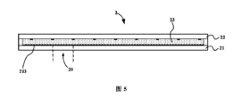
本開示の実施例のアレイ基板21は、調光液晶パネルに適用される。図5に示すように、調光液晶パネル2は、アレイ基板21のほか、アレイ基板21と間隔を置いて設けられる対向基板22と、アレイ基板21と対向基板22との間に位置する液晶層23とをさらに含む。調光液晶パネル2の動作中に、バックライトは、アレイ基板21に入射し、液晶層23を通過して対向基板22から出射する。
The
本開示のいくつかの実施例では、上記の調光液晶パネルは、AD-SDS(ADvanced Super Dimension Switch、先進超次元スイッチ、ADSと略称)モードの液晶パネルである。図3aは、アレイ基板の1つの調光領域の構造を概略的に示す。本開示の実施例によるアレイ基板は、第1透明電極層213のほか、第2透明電極層214をさらに含み、第2透明電極層214は、第1透明電極層213と絶縁されかつ間隔をおいて設けられ、また、第2透明電極層214は、第1透明電極層213よりもアレイ基板の基板(図示せず)に近い。いくつかの実施例では、第2透明電極層214は、画素電極層であってもよく、複数の面状の画素電極を含み、スリット構造2130を有する第1透明電極層213は、共通電極層である。他の実施例では、第2透明電極層は、共通電極層であってもよく、スリット構造を有する第1透明電極層は、画素電極層であり、複数のスリット構造を有する画素電極を含む。
In some embodiments of the present disclosure, the above-mentioned light-adjusting liquid crystal panel is an AD-SDS (Advanced Super Dimension Switch, abbreviated as ADS) mode liquid crystal panel. FIG. 3a shows a schematic structure of one light-adjusting area of the array substrate. The array substrate according to the embodiment of the present disclosure further includes a second
図2a及び図3aに示すように、アレイ基板の構造は、ゲート線211とデータ線212との交差点に設けられ且つそれぞれゲート線211及びデータ線212に接続される薄膜トランジスタ215をさらに含み、具体的には、薄膜トランジスタ215のゲートがゲート線211に接続され、薄膜トランジスタ215のソースがデータ線212に接続され、薄膜トランジスタ215のドレインが画素電極に接続される。また、アレイ基板の構造は、共通電圧信号を共通電極層である第1透明電極層213又は第2透明電極層214により均一に伝送するための共通電極線218をさらに含む。該実施例では、共通電極線218は、隣り合う2本のデータ線212間に設けられる。
As shown in FIG. 2a and FIG. 3a, the structure of the array substrate further includes a
調光液晶パネルの動作中、第1透明電極層213のスリット構造2130のエッジに電場が発生し、第1透明電極層213と第2透明電極層214との間にも電場が発生し、それにより、多次元電場が形成される。該多次元電場は、液晶分子のほとんどを偏向させることができ、それにより、調光液晶パネルの動作効率と透過率を向上させる。
During the operation of the light-adjustable liquid crystal panel, an electric field is generated at the edge of the
図2aに示すように、該実施例では、行方向に沿って配列される薄膜トランジスタ215は、それらのそれぞれに隣接するデータ線212の同側に設けられ、列方向に沿って配列される薄膜トランジスタ215は、それらに隣接するデータ線212の両側に交互に設けられ、データ線212は、交互に両側の画素電極にデータ信号を伝送する。図から分かるように、アレイ基板21に垂直な方向において、各薄膜トランジスタ215は、同じ種類のドメイン3a内に位置し、各薄膜トランジスタ215のドレインは、同じ種類のドメイン内において調光画素の画素電極に接続される。このような駆動設計は、列反転駆動方式(列反転駆動設計において、各薄膜トランジスタのそれぞれは、それに隣接するデータ線の同側に設けられる)に比べて、表示画面のディザリングによる縞を効果的に低減することができる。
2a, in this embodiment, the
表示装置の可視視点の対称性を実現するために、通常、調光領域20の構造は、マルチドメイン設計を用いる。図2a及び図3aに示すように、各々の調光領域20は、第1透明電極層213の複数のドメイン3と重複し、且つ少なくとも2種類のドメインと重複し、また、第1透明電極層213の異なる種類のドメインに位置するスリット構造2130の延在方向は、一定の対称性を示している。このように、電場駆動下で、同じ調光画素において、異なる種類のドメインの液晶分子の配向も一定の対称性を示している。
In order to achieve symmetry of the visible viewpoint of the display device, the structure of the
本開示の実施例では、第1透明電極層213のドメイン3の分割密度は限定されず、表示製品の具体的な仕様サイズに応じて設計が可能である。いくつかの実施例では、ドメインの面積と調光領域の面積との比は、1/16以上であり、且つ1/2以下である。図2aに示す実施例では、ドメイン3の面積と調光領域20の面積との比はほぼ1/8である。第1透明電極層213に含まれるドメイン3の種類も限定されず、例えば図2aに示すように、2種類のドメイン3a、3bを含んでもよいし、2種類のドメイン又はそれ以上の種類のドメインを含んでもよい。
In the embodiments of the present disclosure, the division density of the
図2aに示す実施例では、該複数のドメイン3の形状サイズは同じであり、いずれも二等辺三角形であり、例えば、正三角形であってもよい。該複数のドメイン3は、モザイク状に配置される2種類のドメイン3a、3bを含む。つまり、非エッジに位置するドメイン3aは、3つのドメイン3bで囲まれており、同様に、非エッジに位置するドメイン3bは、3つのドメイン3aで囲まれている。2種類のドメイン3a、3bがモザイク状に配置されており、異なる種類のドメインが均一に乱れされ、マクロ的には、表示装置の表示画面の縞欠陥を改善することができる。
In the embodiment shown in FIG. 2a, the
図2a及び図3aに示す実施例では、各々の調光領域20は、合計、第1透明電極層213の10個のドメイン3(図における符号が1~10のドメインを参照)と重複し、各々の調光領域20は、第1透明電極層213の2種類のドメインといずれも重複する。図1bに示す関連技術では、各々の調光領域20’は、透明電極層213’の4つのドメインと重複し、各々の調光領域20’は、透明電極層213’の2種類のドメイン3a’、3b’といずれも重複する。図2aと図1bとを比較することから、本開示の実施例では、調光領域20と重複するドメイン3の数がより多いことがわかり、調光液晶パネルの調光画素の異なる配向の光に対して、より微細な領域分割が行われることに相当し、それにより、均一に混色する効果が得られ、表示装置の表示画面の縞欠陥が効果的に改善される。
2a and 3a, each dimming
図2aに示すように、本開示の該実施例では、ゲート線211は、行方向に沿って波状の折れ線で延在しており、周期的に配列される複数の第1折れ線ユニット2110を含み、第1折れ線ユニット2110は、列方向を対称軸として対称的に設けられる2つの第1直線部03を含む。データ線212は、列方向に沿って波状の折れ線で延在しており、周期的に配列される複数の第2折れ線ユニット2120を含み、第2折れ線ユニット2120は、中心対称的な第1サブ部分2120aと第2サブ部分2120bとを含み、第1サブ部分2120aと第2サブ部分2120bは、いずれも、行方向を対称軸として対称的に設けられる2つの第2直線部04を含む。該設計を用いることにより、調光液晶パネルの調光画素の形状と表示液晶パネルのサブ画素の形状(通常、長方形)との違いが大きくなり、それにより、モアレの除去に有利になる。該実施例では、各データ線212の形状が完全に同じであり、隣り合うデータ線212の間に共通電極線218が設けられ、共通電極線218は、列方向に沿って波状の折れ線で延在しており、周期的に配列される複数の第3折れ線ユニット2180を含み、第3折れ線ユニット2180は、中心対称的な第3サブ部分2180aと第4サブ部分2180bとを含み、第3サブ部分2180aと第4サブ部分2180bは、いずれも、行方向を対称軸として対称的に設けられる2つの第3直線部05を含む。
2a, in this embodiment of the present disclosure, the
図2aに示すように、本開示のいくつかの実施例では、共通電極線218の形状は、データ線212の形状と概して列方向に対して対称的であり、このようにして、1つの調光領域内において、共通電極層の共通電極線の両側に位置する部分の面積がほぼ等しく、従って、信号一致性が高く、ディスプレイパネル画面の横縞現象を改善するのに有利である。図2bに示すように、本開示の他の実施例では、共通電極線218の形状とデータ線212の形状は、ほぼ同じであってもよい。
As shown in FIG. 2a, in some embodiments of the present disclosure, the shape of the
また、該実施例では、アレイ基板21に垂直な方向において、第1折れ線ユニット2110の端点A1、A2は、第2折れ線ユニット2120の端点B1、B2又は中点B3と重なり、第1折れ線ユニット2110の中点A3は、第3折れ線ユニット2180の端点C1、C2又は中点C3と重なる。各々の調光領域20は、隣り合う2本のゲート線211の一周期の第1折れ線ユニット2110と、隣り合う2本のデータ線212の半周期の第2折れ線ユニット2120とにより画定される。
In addition, in this embodiment, in the direction perpendicular to the
図2aに示すように、該実施例では、ドメイン3の形状は、二等辺三角形である。アレイ基板に垂直な方向において、各々の第1直線部03は、2つのドメイン3の側辺(すなわち、2つの前述した二等辺三角形の同側に位置する等辺)とほぼ重なり、第2折れ線ユニット2120及び第3折れ線ユニット2180の列方向での正投影は、前述した二等辺三角形の高さの4倍にほぼ等しい。
As shown in FIG. 2a, in this embodiment, the shape of the
本開示の該実施例では、図2aに示すように、1つの調光領域20の面積は、8つのドメイン3の面積にほぼ等しい。1つの調光領域20と重複する2種類のドメイン3a、3bの面積は、等しく、ほぼ調光領域20の面積の半分である。各々の調光領域は、10個のドメインと重複し、単一のドメインとの最大重複面積は、該単一のドメインの面積に等しく、すなわち、ほぼ調光領域面積の8分の1である。関連技術に比べて、調光領域の、単一のドメインとの最大重複面積が4分の1減少したので、良好な混色効果が得られ、縞欠陥が効果的に改善される。
In this embodiment of the present disclosure, as shown in FIG. 2a, the area of one
図2a及び図3aに示すように、アレイ基板に垂直な方向において、同じ種類のドメインに位置する第2直線部04及び第3直線部05の延在方向は、スリット構造2130の延在方向と同じである。該設計を用いることにより、第1透明電極層213のスリット構造2130の調光領域20内での配列を最適化させ、より多くのフリンジ電界を発生することができ、調光液晶パネルの透過率の最大化に有利である。いくつかの実施例では、スリット構造2130と列方向とがなす鋭角夾角の範囲は、7°以上であり、且つ11°以下である。
As shown in Figures 2a and 3a, in the direction perpendicular to the array substrate, the extension direction of the second straight portion 04 and the third
図3a、図3b及び図3cに示すように、本開示の一実施例では、第1透明電極層213は、複数の幹電極2131と、幹電極2131の両側に分布する複数の枝電極2132とを含む。各々の幹電極2131は、隣り合う2つの異なる種類のドメインのスリット構造2130の間に位置する。1つのドメイン内において、枝電極2132の延在方向は、スリット構造2130の延在方向と同じであり、隣り合う枝電極2132は、スリット構造2130によって間隔を空けられている。また、複数の幹電極2131のうちの少なくとも1つの幹電極2131は、行方向に沿って延在している。図3bに示すように、該行方向に沿って延在する幹電極2131の両側での複数の枝電極2132は、該幹電極2131に対して対称的に設けられる。図3bに示すように、延在方向と行方向とが所定の夾角をなす幹電極2131の両側での複数の枝電極2132は、該幹電極2131に対して非対称的に設けられる。
As shown in Figures 3a, 3b and 3c, in one embodiment of the present disclosure, the first
上記行方向に沿って延在する幹電極2131は、表示液晶パネルのゲート線の線幅よりも線幅が小さく設計可能である。該アレイ基板を含む調光液晶パネルが表示液晶パネルと組み立てられた後、図4に示すように、表示液晶パネルに垂直な方向において、該行方向に沿って延在する幹電極2131は、表示液晶パネルのゲート線101のエッジの内側に位置することができ、すなわち、該行方向に沿って延在する幹電極2131の表示液晶パネルでの正投影は、ゲート線101の内部と完全に重り、それにより、ゲート線101によって遮蔽される(表示液晶パネルのゲート線101がアレイ基板21の構造ではなく、ここでは、幹電極2131との相対位置関係を例示するためのものに過ぎない)。
The
幹電極2131の両側でのスリット構造2130の延在方向が異なるため、調光画素の液晶分子の、幹電極2131の両側での偏向方向も異なり、幹電極2131には、黒浮き現象がある恐れがある。幹電極2131の線幅を表示液晶パネルのゲート線101の線幅よりも小さく設定し、表示液晶パネルのゲート線101によって遮蔽することで、幹電極2131における黒浮き現象を減少さらに防止することができ、それにより、さらに表示画面の品質を向上させる。
Since the extending directions of the
なお、本開示の他のいくつかの実施例では、表示液晶パネルに垂直な方向において、行方向に沿って延在する幹電極2131は、ゲート線101の幅における部分と重複することができ、それにより、黒浮きを減少させる効果をある程度果たすことができる。
In addition, in some other embodiments of the present disclosure, in the direction perpendicular to the display liquid crystal panel, the
図5に示すように、本開示の実施例は、前述のいずれか技術的解決手段のアレイ基板21と、該アレイ基板21と間隔を置いて設けられる対向基板22と、アレイ基板21と対向基板22との間に位置する液晶層23とを含む、調光液晶パネル2をさらに提供する。
As shown in FIG. 5, an embodiment of the present disclosure further provides a light-adjusting liquid crystal panel 2, which includes an
75インチの調光液晶パネルを例とすると、図6に示すように、左図は、本開示の図2aに示す実施例による調光液晶パネルの画面のシミュレートの局所図であり、右図は、図1bに示す関連技術での調光液晶パネルの画面のシミュレートの局所図である。関連技術での調光液晶パネルのシミュレート画面から、明らかな縞が見えるが、本開示の実施例での調光液晶パネルのシミュレート画面から、あまり縞が見えず、表示品質が著しく向上していることが分かる。 Taking a 75-inch light-adjustable LCD panel as an example, as shown in FIG. 6, the left figure is a localized view of the simulated screen of the light-adjustable LCD panel according to the embodiment shown in FIG. 2a of the present disclosure, and the right figure is a localized view of the simulated screen of the light-adjustable LCD panel in the related art shown in FIG. 1b. While obvious stripes are visible on the simulated screen of the light-adjustable LCD panel in the related art, few stripes are visible on the simulated screen of the light-adjustable LCD panel in the embodiment of the present disclosure, and it can be seen that the display quality has been significantly improved.
図7に示すように、本開示の実施例は、ディスプレイパネル100をさらに提供し、ディスプレイパネル100は、前述実施例の調光液晶パネル2と、調光液晶パネル2の一側に位置する表示液晶パネル1とを含む。具体的には、表示液晶パネル1は、調光液晶パネル2の出光側に位置する。
As shown in FIG. 7, an embodiment of the present disclosure further provides a
該ディスプレイパネルは、表示装置に適用され、画面に対してより微細な領域調光を行うことができ、コントラスト表現が優れており、関連技術に比べて、画面の縞欠陥も効果的に改善されているため、画面品質が高く、ユーザー体験を著しく向上させる。表示装置の具体的な製品の種類は限定されず、例えば、ディスプレイ、タブレットコンピュータ、ノートパソコン、テレビ、ATM機器、電子ペーパー、ディスプレイスクリーンなどであり得る。 The display panel is applied to a display device, and can perform finer area dimming on the screen, has excellent contrast expression, and effectively improves the stripe defects on the screen compared to related technologies, resulting in high screen quality and significantly improving the user experience. Specific product types of the display device are not limited, and can be, for example, displays, tablet computers, notebook computers, televisions, ATM machines, electronic paper, display screens, etc.
いくつかの実施例では、上記のように、調光液晶パネルのアレイ基板の第1透明電極層は、複数の幹電極と、幹電極の両側に分布している複数の枝電極とを含み、各々の幹電極は、隣り合う2つの異なる種類のドメインのスリット構造の間に位置する。1つのドメイン内において、枝電極の延在方向は、スリット構造の延在方向と同じであり、隣り合う枝電極は、スリット構造によって間隔を空けられている。少なくとも1つの幹電極は、行方向に沿って延在しており、且つ行方向に沿って延在する幹電極の線幅は、表示液晶パネルのゲート線の線幅未満であり、表示液晶パネルに垂直な方向において、行方向に沿って延在する幹電極は、表示液晶パネルのゲート線のエッジの内側に位置する。他の実施例では、表示液晶パネルに垂直な方向において、行方向に沿って延在する幹電極は、表示液晶パネルのゲート線と一部的に重なってもよい。これらの実施例の設計案を用いることにより、幹電極における黒浮き現象を効果的に減少さらに防止でき、それにより、さらに表示画面の品質を向上させることができる。 In some embodiments, as described above, the first transparent electrode layer of the array substrate of the light control liquid crystal panel includes a plurality of stem electrodes and a plurality of branch electrodes distributed on both sides of the stem electrodes, and each stem electrode is located between the slit structures of two different kinds of adjacent domains. In one domain, the extension direction of the branch electrodes is the same as the extension direction of the slit structures, and the adjacent branch electrodes are spaced apart by the slit structures. At least one stem electrode extends along the row direction, and the line width of the stem electrode extending along the row direction is less than the line width of the gate line of the display liquid crystal panel, and in a direction perpendicular to the display liquid crystal panel, the stem electrode extending along the row direction is located inside the edge of the gate line of the display liquid crystal panel. In other embodiments, in a direction perpendicular to the display liquid crystal panel, the stem electrode extending along the row direction may partially overlap the gate line of the display liquid crystal panel. By using the design proposals of these embodiments, the black floating phenomenon in the stem electrodes can be effectively reduced or even prevented, thereby further improving the quality of the display screen.
以上、本開示の実施形態について詳細に説明する。本開示のアイデアを不明瞭にすることを避けるために、本分野における知られている詳細は説明されていない。当業者は、上記の説明に従って、ここに開示された技術案をどのように実施するかを完全に理解することができる。 The above describes the embodiments of the present disclosure in detail. Details known in the art are not described to avoid obscuring the ideas of the present disclosure. Those skilled in the art can fully understand how to implement the technical proposals disclosed herein according to the above description.
当業者であれば理解できるように、本開示のいくつかの特定の実施形態を例に挙げて詳細に説明したが、上記例は、本開示の範囲を限定するものではなく、上記の例を説明するためのものに過ぎない。当業者であれば理解できるように、本開示の範囲および精神から逸脱することなく、上記実施形態を修正したり、一部の技術的特徴を均等に置換したりすることができる。本開示の範囲は、添付の特許請求の範囲によって限定される。 Although some specific embodiments of the present disclosure have been described in detail with examples, the above examples are not intended to limit the scope of the present disclosure, but are merely intended to illustrate the above examples. As can be understood by those skilled in the art, the above embodiments can be modified or some technical features can be substituted equally without departing from the scope and spirit of the present disclosure. The scope of the present disclosure is limited by the scope of the appended claims.
Claims (16)
複数のスリット構造を有する第1透明電極層と、行方向に沿って延在する複数本のゲート線と、列方向に沿って延在する複数本のデータ線とを含み
第1透明電極層は、面積が等しい複数のドメインを含み、前記複数のドメインは、モザイク状に配置される少なくとも2種類のドメインを含み、同じ種類の前記ドメインに位置する前記スリット構造の延在方向が同じであり、異なる種類の前記ドメインに位置する前記スリット構造の延在方向が異なり、
前記複数本のゲート線と前記複数本のデータ線とが交差して、アレイ状に配置される複数の調光領域を画定し、各々の前記調光領域が前記第1透明電極層の少なくとも2種類の前記ドメインと重複し、
前記ゲート線は、行方向に沿って波状の折れ線で延在しており、周期的に配列される複数の第1折れ線ユニットを含み、前記第1折れ線ユニットは、列方向を対称軸として対称的に設けられる2つの第1直線部を含み、
前記データ線は、列方向に沿って波状の折れ線で延在しており、周期的に配列される複数の第2折れ線ユニットを含み、前記第2折れ線ユニットは、中心対称的な第1サブ部分と第2サブ部分とを含み、前記第1サブ部分と前記第2サブ部分は、いずれも、行方向を対称軸として対称的に設けられる2つの第2直線部を含み、
前記アレイ基板は、隣り合う2本の前記データ線間に位置する共通電極線をさらに含み、前記共通電極線は、列方向に沿って波状の折れ線で延在しており、周期的に配列される複数の第3折れ線ユニットを含み、前記第3折れ線ユニットは、中心対称的な第3サブ部分と第4サブ部分とを含み、前記第3サブ部分と前記第4サブ部分は、いずれも、行方向を対称軸として対称的に設けられる2つの第3直線部を含む、アレイ基板。 An array substrate,
The present invention relates to a pixel array comprising: a first transparent electrode layer having a plurality of slit structures; a plurality of gate lines extending along a row direction; and a plurality of data lines extending along a column direction; the first transparent electrode layer includes a plurality of domains having the same area, the plurality of domains including at least two types of domains arranged in a mosaic pattern, the slit structures located in the same type of domains have the same extension direction, and the slit structures located in the different types of domains have different extension directions;
The gate lines and the data lines intersect to define a plurality of light control regions arranged in an array, and each of the light control regions overlaps with at least two types of the domains of the first transparent electrode layer ;
the gate line extends in a row direction as a wavy bent line and includes a plurality of first bent line units that are periodically arranged, and the first bent line unit includes two first straight line portions that are symmetrically arranged with respect to the column direction;
the data line extends in a wavy folded line along a column direction and includes a plurality of second folded line units that are periodically arranged, the second folded line unit includes a first sub-portion and a second sub-portion that are symmetrical with respect to a center, and each of the first sub-portion and the second sub-portion includes two second straight line portions that are symmetrically arranged with respect to a row direction as an axis of symmetry;
the array substrate further includes a common electrode line located between two adjacent data lines, the common electrode line extending in a wavy folded line along the column direction and including a plurality of periodically arranged third folded line units, the third folded line unit including a centrosymmetric third sub-portion and a fourth sub-portion, each of the third sub-portion and the fourth sub-portion including two third straight line portions symmetrically arranged with respect to the row direction as an axis of symmetry .
前記第2折れ線ユニット及び前記第3折れ線ユニットの列方向での正投影は、前記二等辺三角形の高さの4倍にほぼ等しい、請求項7に記載のアレイ基板。 In a direction perpendicular to the array substrate, each of the first straight line portions substantially overlaps with an equal side of each of the two isosceles triangles located on the same side;
The array substrate according to claim 7 , wherein the orthogonal projections of the second and third bent-line units in the column direction are approximately equal to four times the height of the isosceles triangle.
各々の前記幹電極は、隣り合う2つの異なる種類の前記ドメインのスリット構造の間に位置し、
1つの前記ドメイン内において、前記枝電極の延在方向は、前記スリット構造の延在方向と同じであり、隣り合う前記枝電極は、前記スリット構造によって間隔を空けられており、
少なくとも1つの前記幹電極は、行方向に沿って延在している、請求項1に記載のアレイ基板。 the first transparent electrode layer includes a plurality of stem electrodes and a plurality of branch electrodes connected to the stem electrodes on both sides of each of the stem electrodes;
Each of the trunk electrodes is located between the slit structures of two adjacent different types of the domains;
In one of the domains, the extension direction of the branch electrodes is the same as the extension direction of the slit structure, and adjacent branch electrodes are spaced apart by the slit structure;
The array substrate according to claim 1 , wherein at least one of the stem electrodes extends along a row direction.
前記アレイ基板に垂直な方向から見た際に、一の行方向に沿って配列される前記薄膜トランジスタは、それらに隣接する前記データ線に対して同じ側に設けられ、
前記アレイ基板に垂直な方向から見た際に、一の列方向に沿って配列される前記薄膜トランジスタは、それらに隣接する前記データ線に対して一方の側と他方の側とに交互に設けられる、請求項1に記載のアレイ基板。 thin film transistors are provided near intersections of the gate lines and the data lines , and are connected to the gate lines and the data lines, respectively ;
When viewed from a direction perpendicular to the array substrate, the thin film transistors arranged along one row direction are provided on the same side with respect to the data lines adjacent thereto ;
2. The array substrate according to claim 1, wherein, when viewed from a direction perpendicular to the array substrate, the thin film transistors arranged along a column direction are alternately provided on one side and the other side of the data lines adjacent thereto.
各々の前記幹電極は、隣り合う2つの異なる種類の前記ドメインのスリット構造の間に位置し、
1つの前記ドメイン内において、前記枝電極の延在方向は、前記スリット構造の延在方向と同じであり、隣り合う前記枝電極は、前記スリット構造によって間隔を空けられており、
少なくとも1つの前記幹電極は、行方向に沿って延在しており、且つ行方向に沿って延在する前記幹電極の線幅が前記表示液晶パネルのゲート線の線幅未満であり、前記表示液晶パネルに垂直な方向において、行方向に沿って延在する前記幹電極は、前記表示液晶パネルのゲート線と少なくとも部分的に重なる、請求項14に記載のディスプレイパネル。 the first transparent electrode layer includes a plurality of stem electrodes and a plurality of branch electrodes connected to the stem electrodes on both sides of each of the stem electrodes;
Each of the trunk electrodes is located between the slit structures of two adjacent different types of the domains;
In one of the domains, the extension direction of the branch electrodes is the same as the extension direction of the slit structure, and adjacent branch electrodes are spaced apart by the slit structure;
15. The display panel of claim 14, wherein at least one of the stem electrodes extends along a row direction, and the line width of the stem electrode extending along the row direction is less than the line width of a gate line of the display liquid crystal panel, and in a direction perpendicular to the display liquid crystal panel, the stem electrode extending along the row direction at least partially overlaps with the gate line of the display liquid crystal panel.
Applications Claiming Priority (1)
| Application Number | Priority Date | Filing Date | Title |
|---|---|---|---|
| PCT/CN2019/121437 WO2021102769A1 (en) | 2019-11-28 | 2019-11-28 | Array substrate, dimming liquid crystal panel and display panel |
Publications (3)
| Publication Number | Publication Date |
|---|---|
| JP2023512368A JP2023512368A (en) | 2023-03-27 |
| JPWO2021102769A5 JPWO2021102769A5 (en) | 2024-03-25 |
| JP7477533B2 true JP7477533B2 (en) | 2024-05-01 |
Family
ID=76129747
Family Applications (1)
| Application Number | Title | Priority Date | Filing Date |
|---|---|---|---|
| JP2021568021A Active JP7477533B2 (en) | 2019-11-28 | 2019-11-28 | Array substrate, light-adjusting liquid crystal panel, and display panel |
Country Status (5)
| Country | Link |
|---|---|
| US (1) | US11487175B2 (en) |
| EP (2) | EP4361714A2 (en) |
| JP (1) | JP7477533B2 (en) |
| CN (1) | CN113260912B (en) |
| WO (1) | WO2021102769A1 (en) |
Families Citing this family (3)
| Publication number | Priority date | Publication date | Assignee | Title |
|---|---|---|---|---|
| CN110780500A (en) * | 2019-11-15 | 2020-02-11 | 京东方科技集团股份有限公司 | Array substrate, light control panel and display device |
| WO2021102816A1 (en) * | 2019-11-28 | 2021-06-03 | 京东方科技集团股份有限公司 | Array substrate, dimming liquid crystal panel, and display panel |
| TWI809999B (en) * | 2022-07-29 | 2023-07-21 | 友達光電股份有限公司 | Display |
Citations (7)
| Publication number | Priority date | Publication date | Assignee | Title |
|---|---|---|---|---|
| JP2007047664A (en) | 2005-08-12 | 2007-02-22 | Hitachi Displays Ltd | Display apparatus |
| JP2009237229A (en) | 2008-03-27 | 2009-10-15 | Epson Imaging Devices Corp | Liquid crystal display and electronic apparatus |
| JP2015049454A (en) | 2013-09-03 | 2015-03-16 | 三菱電機株式会社 | Liquid crystal display unit and array substrate |
| JP2018072839A (en) | 2016-10-31 | 2018-05-10 | エルジー ディスプレイ カンパニー リミテッド | Liquid crystal display having light valve |
| CN108983463A (en) | 2018-08-29 | 2018-12-11 | 京东方科技集团股份有限公司 | Display panel and display device |
| US20190302543A1 (en) | 2018-04-02 | 2019-10-03 | Au Optronics Corporation | Display device |
| CN110361899A (en) | 2019-06-27 | 2019-10-22 | 厦门天马微电子有限公司 | A kind of display device |
Family Cites Families (7)
| Publication number | Priority date | Publication date | Assignee | Title |
|---|---|---|---|---|
| JP4961077B2 (en) | 2001-03-15 | 2012-06-27 | 大日本印刷株式会社 | Electrode substrate for liquid crystal display device and manufacturing method thereof |
| KR101229413B1 (en) * | 2006-04-18 | 2013-02-04 | 엘지디스플레이 주식회사 | An array substrate for In-Plane switching mode LCD and method of fabricating of the same |
| CN105549280B (en) * | 2016-02-29 | 2018-10-30 | 京东方科技集团股份有限公司 | Dot structure, array substrate and display device |
| JP6855305B2 (en) * | 2017-03-31 | 2021-04-07 | 株式会社ジャパンディスプレイ | Display device |
| TWI680326B (en) * | 2018-09-28 | 2019-12-21 | 友達光電股份有限公司 | Display |
| CN109597232A (en) * | 2019-01-10 | 2019-04-09 | 昆山龙腾光电有限公司 | Backlight module, backlight adjusting method and display device |
| CN112669742A (en) * | 2019-10-16 | 2021-04-16 | 群创光电股份有限公司 | Display device |
-
2019
- 2019-11-28 EP EP24162772.8A patent/EP4361714A2/en active Pending
- 2019-11-28 WO PCT/CN2019/121437 patent/WO2021102769A1/en unknown
- 2019-11-28 JP JP2021568021A patent/JP7477533B2/en active Active
- 2019-11-28 EP EP19945423.2A patent/EP4067985B1/en active Active
- 2019-11-28 CN CN201980002624.8A patent/CN113260912B/en active Active
- 2019-11-28 US US16/975,264 patent/US11487175B2/en active Active
Patent Citations (7)
| Publication number | Priority date | Publication date | Assignee | Title |
|---|---|---|---|---|
| JP2007047664A (en) | 2005-08-12 | 2007-02-22 | Hitachi Displays Ltd | Display apparatus |
| JP2009237229A (en) | 2008-03-27 | 2009-10-15 | Epson Imaging Devices Corp | Liquid crystal display and electronic apparatus |
| JP2015049454A (en) | 2013-09-03 | 2015-03-16 | 三菱電機株式会社 | Liquid crystal display unit and array substrate |
| JP2018072839A (en) | 2016-10-31 | 2018-05-10 | エルジー ディスプレイ カンパニー リミテッド | Liquid crystal display having light valve |
| US20190302543A1 (en) | 2018-04-02 | 2019-10-03 | Au Optronics Corporation | Display device |
| CN108983463A (en) | 2018-08-29 | 2018-12-11 | 京东方科技集团股份有限公司 | Display panel and display device |
| CN110361899A (en) | 2019-06-27 | 2019-10-22 | 厦门天马微电子有限公司 | A kind of display device |
Also Published As
| Publication number | Publication date |
|---|---|
| CN113260912A (en) | 2021-08-13 |
| US11487175B2 (en) | 2022-11-01 |
| JP2023512368A (en) | 2023-03-27 |
| WO2021102769A1 (en) | 2021-06-03 |
| WO2021102769A9 (en) | 2021-11-11 |
| US20220137470A1 (en) | 2022-05-05 |
| CN113260912B (en) | 2023-01-13 |
| EP4067985A1 (en) | 2022-10-05 |
| EP4067985B1 (en) | 2024-05-08 |
| EP4067985A4 (en) | 2022-11-23 |
| EP4361714A2 (en) | 2024-05-01 |
Similar Documents
| Publication | Publication Date | Title |
|---|---|---|
| US9551906B2 (en) | Liquid crystal display | |
| TWI507799B (en) | Display devices and electronic machines | |
| TWI484272B (en) | Pixel structure of transparent liquid crystal display panel | |
| US8462080B2 (en) | Display device displaying single or dual images and method of driving the same | |
| JP6105602B2 (en) | Array substrate for display device, color filter substrate, and manufacturing method thereof | |
| JP5253585B2 (en) | Liquid crystal display | |
| JP7477533B2 (en) | Array substrate, light-adjusting liquid crystal panel, and display panel | |
| KR101219319B1 (en) | Liquid crystal display device | |
| CN109343263B (en) | COA type liquid crystal display | |
| GB2409094A (en) | In-plane switching mode liquid crystal display device and method of fabricating the same | |
| WO2021077510A1 (en) | Pixel structure and liquid crystal display panel | |
| WO2021036499A1 (en) | Display panel and display device | |
| JP2005173540A (en) | Fringe field switching mode liquid crystal display device | |
| KR101897744B1 (en) | In-Plane Switching mode Liquid crystal display device | |
| CN113518943B (en) | Array substrate, dimming liquid crystal panel and display panel | |
| TWI591408B (en) | Pixel structure of transparent liquid crystal display panel | |
| US11914236B2 (en) | Liquid crystal display device | |
| US20240111195A1 (en) | Liquid crystal display device | |
| US20200081293A1 (en) | Pixel arrangement and method for manufacturing display panel | |
| CN110967853A (en) | Display panel, display device and driving method of display panel |
Legal Events
| Date | Code | Title | Description |
|---|---|---|---|
| A621 | Written request for application examination |
Free format text: JAPANESE INTERMEDIATE CODE: A621 Effective date: 20221125 |
|
| A977 | Report on retrieval |
Free format text: JAPANESE INTERMEDIATE CODE: A971007 Effective date: 20231129 |
|
| A131 | Notification of reasons for refusal |
Free format text: JAPANESE INTERMEDIATE CODE: A131 Effective date: 20231211 |
|
| A524 | Written submission of copy of amendment under article 19 pct |
Free format text: JAPANESE INTERMEDIATE CODE: A524 Effective date: 20240311 |
|
| TRDD | Decision of grant or rejection written | ||
| A01 | Written decision to grant a patent or to grant a registration (utility model) |
Free format text: JAPANESE INTERMEDIATE CODE: A01 Effective date: 20240325 |
|
| A61 | First payment of annual fees (during grant procedure) |
Free format text: JAPANESE INTERMEDIATE CODE: A61 Effective date: 20240418 |
|
| R150 | Certificate of patent or registration of utility model |
Ref document number: 7477533 Country of ref document: JP Free format text: JAPANESE INTERMEDIATE CODE: R150 |