JP7475973B2 - Optical Encoder and Control Device - Google Patents
Optical Encoder and Control Device Download PDFInfo
- Publication number
- JP7475973B2 JP7475973B2 JP2020099491A JP2020099491A JP7475973B2 JP 7475973 B2 JP7475973 B2 JP 7475973B2 JP 2020099491 A JP2020099491 A JP 2020099491A JP 2020099491 A JP2020099491 A JP 2020099491A JP 7475973 B2 JP7475973 B2 JP 7475973B2
- Authority
- JP
- Japan
- Prior art keywords
- light receiving
- receiving element
- signal
- diffraction grating
- light
- Prior art date
- Legal status (The legal status is an assumption and is not a legal conclusion. Google has not performed a legal analysis and makes no representation as to the accuracy of the status listed.)
- Active
Links
- 230000003287 optical effect Effects 0.000 title claims description 50
- 238000001514 detection method Methods 0.000 claims description 55
- 238000012545 processing Methods 0.000 claims description 41
- 230000007423 decrease Effects 0.000 claims description 6
- 238000000034 method Methods 0.000 claims description 6
- 230000008569 process Effects 0.000 claims description 6
- 238000006073 displacement reaction Methods 0.000 claims description 3
- 238000010586 diagram Methods 0.000 description 20
- 238000006243 chemical reaction Methods 0.000 description 9
- 230000005540 biological transmission Effects 0.000 description 6
- 230000000630 rising effect Effects 0.000 description 6
- 230000000052 comparative effect Effects 0.000 description 5
- 230000000737 periodic effect Effects 0.000 description 5
- 230000008859 change Effects 0.000 description 4
- 238000003708 edge detection Methods 0.000 description 4
- 230000000694 effects Effects 0.000 description 4
- 230000000903 blocking effect Effects 0.000 description 3
- 238000011161 development Methods 0.000 description 3
- 239000006059 cover glass Substances 0.000 description 2
- 238000013461 design Methods 0.000 description 2
- 230000007246 mechanism Effects 0.000 description 2
- 230000002093 peripheral effect Effects 0.000 description 2
- 239000004065 semiconductor Substances 0.000 description 2
- VYZAMTAEIAYCRO-UHFFFAOYSA-N Chromium Chemical compound [Cr] VYZAMTAEIAYCRO-UHFFFAOYSA-N 0.000 description 1
- 238000009825 accumulation Methods 0.000 description 1
- XAGFODPZIPBFFR-UHFFFAOYSA-N aluminium Chemical compound [Al] XAGFODPZIPBFFR-UHFFFAOYSA-N 0.000 description 1
- 229910052782 aluminium Inorganic materials 0.000 description 1
- 238000003491 array Methods 0.000 description 1
- 239000012141 concentrate Substances 0.000 description 1
- 125000004122 cyclic group Chemical group 0.000 description 1
- 230000007547 defect Effects 0.000 description 1
- 230000004069 differentiation Effects 0.000 description 1
- 239000000428 dust Substances 0.000 description 1
- 238000005530 etching Methods 0.000 description 1
- 238000012986 modification Methods 0.000 description 1
- 230000004048 modification Effects 0.000 description 1
- 239000010453 quartz Substances 0.000 description 1
- 239000011347 resin Substances 0.000 description 1
- 229920005989 resin Polymers 0.000 description 1
- 230000004044 response Effects 0.000 description 1
- VYPSYNLAJGMNEJ-UHFFFAOYSA-N silicon dioxide Inorganic materials O=[Si]=O VYPSYNLAJGMNEJ-UHFFFAOYSA-N 0.000 description 1
- 239000000758 substrate Substances 0.000 description 1
Images


Classifications
-
- G—PHYSICS
- G01—MEASURING; TESTING
- G01D—MEASURING NOT SPECIALLY ADAPTED FOR A SPECIFIC VARIABLE; ARRANGEMENTS FOR MEASURING TWO OR MORE VARIABLES NOT COVERED IN A SINGLE OTHER SUBCLASS; TARIFF METERING APPARATUS; MEASURING OR TESTING NOT OTHERWISE PROVIDED FOR
- G01D5/00—Mechanical means for transferring the output of a sensing member; Means for converting the output of a sensing member to another variable where the form or nature of the sensing member does not constrain the means for converting; Transducers not specially adapted for a specific variable
- G01D5/26—Mechanical means for transferring the output of a sensing member; Means for converting the output of a sensing member to another variable where the form or nature of the sensing member does not constrain the means for converting; Transducers not specially adapted for a specific variable characterised by optical transfer means, i.e. using infrared, visible, or ultraviolet light
- G01D5/28—Mechanical means for transferring the output of a sensing member; Means for converting the output of a sensing member to another variable where the form or nature of the sensing member does not constrain the means for converting; Transducers not specially adapted for a specific variable characterised by optical transfer means, i.e. using infrared, visible, or ultraviolet light with deflection of beams of light, e.g. for direct optical indication
- G01D5/30—Mechanical means for transferring the output of a sensing member; Means for converting the output of a sensing member to another variable where the form or nature of the sensing member does not constrain the means for converting; Transducers not specially adapted for a specific variable characterised by optical transfer means, i.e. using infrared, visible, or ultraviolet light with deflection of beams of light, e.g. for direct optical indication the beams of light being detected by photocells
-
- G—PHYSICS
- G01—MEASURING; TESTING
- G01D—MEASURING NOT SPECIALLY ADAPTED FOR A SPECIFIC VARIABLE; ARRANGEMENTS FOR MEASURING TWO OR MORE VARIABLES NOT COVERED IN A SINGLE OTHER SUBCLASS; TARIFF METERING APPARATUS; MEASURING OR TESTING NOT OTHERWISE PROVIDED FOR
- G01D5/00—Mechanical means for transferring the output of a sensing member; Means for converting the output of a sensing member to another variable where the form or nature of the sensing member does not constrain the means for converting; Transducers not specially adapted for a specific variable
- G01D5/26—Mechanical means for transferring the output of a sensing member; Means for converting the output of a sensing member to another variable where the form or nature of the sensing member does not constrain the means for converting; Transducers not specially adapted for a specific variable characterised by optical transfer means, i.e. using infrared, visible, or ultraviolet light
- G01D5/32—Mechanical means for transferring the output of a sensing member; Means for converting the output of a sensing member to another variable where the form or nature of the sensing member does not constrain the means for converting; Transducers not specially adapted for a specific variable characterised by optical transfer means, i.e. using infrared, visible, or ultraviolet light with attenuation or whole or partial obturation of beams of light
- G01D5/34—Mechanical means for transferring the output of a sensing member; Means for converting the output of a sensing member to another variable where the form or nature of the sensing member does not constrain the means for converting; Transducers not specially adapted for a specific variable characterised by optical transfer means, i.e. using infrared, visible, or ultraviolet light with attenuation or whole or partial obturation of beams of light the beams of light being detected by photocells
- G01D5/347—Mechanical means for transferring the output of a sensing member; Means for converting the output of a sensing member to another variable where the form or nature of the sensing member does not constrain the means for converting; Transducers not specially adapted for a specific variable characterised by optical transfer means, i.e. using infrared, visible, or ultraviolet light with attenuation or whole or partial obturation of beams of light the beams of light being detected by photocells using displacement encoding scales
- G01D5/34707—Scales; Discs, e.g. fixation, fabrication, compensation
-
- G—PHYSICS
- G01—MEASURING; TESTING
- G01D—MEASURING NOT SPECIALLY ADAPTED FOR A SPECIFIC VARIABLE; ARRANGEMENTS FOR MEASURING TWO OR MORE VARIABLES NOT COVERED IN A SINGLE OTHER SUBCLASS; TARIFF METERING APPARATUS; MEASURING OR TESTING NOT OTHERWISE PROVIDED FOR
- G01D5/00—Mechanical means for transferring the output of a sensing member; Means for converting the output of a sensing member to another variable where the form or nature of the sensing member does not constrain the means for converting; Transducers not specially adapted for a specific variable
- G01D5/26—Mechanical means for transferring the output of a sensing member; Means for converting the output of a sensing member to another variable where the form or nature of the sensing member does not constrain the means for converting; Transducers not specially adapted for a specific variable characterised by optical transfer means, i.e. using infrared, visible, or ultraviolet light
- G01D5/32—Mechanical means for transferring the output of a sensing member; Means for converting the output of a sensing member to another variable where the form or nature of the sensing member does not constrain the means for converting; Transducers not specially adapted for a specific variable characterised by optical transfer means, i.e. using infrared, visible, or ultraviolet light with attenuation or whole or partial obturation of beams of light
- G01D5/34—Mechanical means for transferring the output of a sensing member; Means for converting the output of a sensing member to another variable where the form or nature of the sensing member does not constrain the means for converting; Transducers not specially adapted for a specific variable characterised by optical transfer means, i.e. using infrared, visible, or ultraviolet light with attenuation or whole or partial obturation of beams of light the beams of light being detected by photocells
- G01D5/36—Forming the light into pulses
- G01D5/38—Forming the light into pulses by diffraction gratings
-
- G—PHYSICS
- G01—MEASURING; TESTING
- G01B—MEASURING LENGTH, THICKNESS OR SIMILAR LINEAR DIMENSIONS; MEASURING ANGLES; MEASURING AREAS; MEASURING IRREGULARITIES OF SURFACES OR CONTOURS
- G01B11/00—Measuring arrangements characterised by the use of optical techniques
- G01B11/26—Measuring arrangements characterised by the use of optical techniques for measuring angles or tapers; for testing the alignment of axes
-
- G—PHYSICS
- G01—MEASURING; TESTING
- G01D—MEASURING NOT SPECIALLY ADAPTED FOR A SPECIFIC VARIABLE; ARRANGEMENTS FOR MEASURING TWO OR MORE VARIABLES NOT COVERED IN A SINGLE OTHER SUBCLASS; TARIFF METERING APPARATUS; MEASURING OR TESTING NOT OTHERWISE PROVIDED FOR
- G01D5/00—Mechanical means for transferring the output of a sensing member; Means for converting the output of a sensing member to another variable where the form or nature of the sensing member does not constrain the means for converting; Transducers not specially adapted for a specific variable
- G01D5/26—Mechanical means for transferring the output of a sensing member; Means for converting the output of a sensing member to another variable where the form or nature of the sensing member does not constrain the means for converting; Transducers not specially adapted for a specific variable characterised by optical transfer means, i.e. using infrared, visible, or ultraviolet light
- G01D5/28—Mechanical means for transferring the output of a sensing member; Means for converting the output of a sensing member to another variable where the form or nature of the sensing member does not constrain the means for converting; Transducers not specially adapted for a specific variable characterised by optical transfer means, i.e. using infrared, visible, or ultraviolet light with deflection of beams of light, e.g. for direct optical indication
- G01D5/285—Mechanical means for transferring the output of a sensing member; Means for converting the output of a sensing member to another variable where the form or nature of the sensing member does not constrain the means for converting; Transducers not specially adapted for a specific variable characterised by optical transfer means, i.e. using infrared, visible, or ultraviolet light with deflection of beams of light, e.g. for direct optical indication using a movable mirror
-
- G—PHYSICS
- G01—MEASURING; TESTING
- G01D—MEASURING NOT SPECIALLY ADAPTED FOR A SPECIFIC VARIABLE; ARRANGEMENTS FOR MEASURING TWO OR MORE VARIABLES NOT COVERED IN A SINGLE OTHER SUBCLASS; TARIFF METERING APPARATUS; MEASURING OR TESTING NOT OTHERWISE PROVIDED FOR
- G01D5/00—Mechanical means for transferring the output of a sensing member; Means for converting the output of a sensing member to another variable where the form or nature of the sensing member does not constrain the means for converting; Transducers not specially adapted for a specific variable
- G01D5/26—Mechanical means for transferring the output of a sensing member; Means for converting the output of a sensing member to another variable where the form or nature of the sensing member does not constrain the means for converting; Transducers not specially adapted for a specific variable characterised by optical transfer means, i.e. using infrared, visible, or ultraviolet light
- G01D5/32—Mechanical means for transferring the output of a sensing member; Means for converting the output of a sensing member to another variable where the form or nature of the sensing member does not constrain the means for converting; Transducers not specially adapted for a specific variable characterised by optical transfer means, i.e. using infrared, visible, or ultraviolet light with attenuation or whole or partial obturation of beams of light
- G01D5/34—Mechanical means for transferring the output of a sensing member; Means for converting the output of a sensing member to another variable where the form or nature of the sensing member does not constrain the means for converting; Transducers not specially adapted for a specific variable characterised by optical transfer means, i.e. using infrared, visible, or ultraviolet light with attenuation or whole or partial obturation of beams of light the beams of light being detected by photocells
- G01D5/347—Mechanical means for transferring the output of a sensing member; Means for converting the output of a sensing member to another variable where the form or nature of the sensing member does not constrain the means for converting; Transducers not specially adapted for a specific variable characterised by optical transfer means, i.e. using infrared, visible, or ultraviolet light with attenuation or whole or partial obturation of beams of light the beams of light being detected by photocells using displacement encoding scales
- G01D5/34746—Linear encoders
-
- G—PHYSICS
- G01—MEASURING; TESTING
- G01D—MEASURING NOT SPECIALLY ADAPTED FOR A SPECIFIC VARIABLE; ARRANGEMENTS FOR MEASURING TWO OR MORE VARIABLES NOT COVERED IN A SINGLE OTHER SUBCLASS; TARIFF METERING APPARATUS; MEASURING OR TESTING NOT OTHERWISE PROVIDED FOR
- G01D5/00—Mechanical means for transferring the output of a sensing member; Means for converting the output of a sensing member to another variable where the form or nature of the sensing member does not constrain the means for converting; Transducers not specially adapted for a specific variable
- G01D5/26—Mechanical means for transferring the output of a sensing member; Means for converting the output of a sensing member to another variable where the form or nature of the sensing member does not constrain the means for converting; Transducers not specially adapted for a specific variable characterised by optical transfer means, i.e. using infrared, visible, or ultraviolet light
- G01D5/32—Mechanical means for transferring the output of a sensing member; Means for converting the output of a sensing member to another variable where the form or nature of the sensing member does not constrain the means for converting; Transducers not specially adapted for a specific variable characterised by optical transfer means, i.e. using infrared, visible, or ultraviolet light with attenuation or whole or partial obturation of beams of light
- G01D5/34—Mechanical means for transferring the output of a sensing member; Means for converting the output of a sensing member to another variable where the form or nature of the sensing member does not constrain the means for converting; Transducers not specially adapted for a specific variable characterised by optical transfer means, i.e. using infrared, visible, or ultraviolet light with attenuation or whole or partial obturation of beams of light the beams of light being detected by photocells
- G01D5/347—Mechanical means for transferring the output of a sensing member; Means for converting the output of a sensing member to another variable where the form or nature of the sensing member does not constrain the means for converting; Transducers not specially adapted for a specific variable characterised by optical transfer means, i.e. using infrared, visible, or ultraviolet light with attenuation or whole or partial obturation of beams of light the beams of light being detected by photocells using displacement encoding scales
- G01D5/34776—Absolute encoders with analogue or digital scales
- G01D5/34792—Absolute encoders with analogue or digital scales with only digital scales or both digital and incremental scales
Description
本発明は、光学式エンコーダ及び制御装置に関する。 The present invention relates to an optical encoder and a control device.
従来から、工作機やFA装置などにおける位置検出装置として、エンコーダが用いられている。インクリメント方式のエンコーダでは、スケール上の特定位置に設けられた基準マークを利用して、原点などの基準位置を検出し、その基準位置からの相対移動量に基づいてストローク内の位置を検出する。 Encoders have traditionally been used as position detection devices in machine tools, factory automation equipment, and the like. Incremental encoders use a reference mark provided at a specific position on a scale to detect a reference position such as the origin, and detect the position within the stroke based on the amount of relative movement from that reference position.
特許文献1には、スケール上の基準位置を検出するエンコーダが開示されている。当該エンコーダでは、回折レンズ構造を用い、分割フォトダイオードで差動信号を得ることで、ノイズに強く、再現性の高いエッジ検出を可能にしている。
特許文献1に記載のエンコーダでは、回折レンズ構造によって集光するスポット位置に光量が集中することで、その周辺は逆に光量が低下する。スポット位置付近の光強度分布から基準位置を検出する場合、周辺の光量低下により検出精度が低下する問題がある。
In the encoder described in
そこで本発明は、高精度に基準位置を検出する光学式エンコーダを提供することを目的とする。 The present invention aims to provide an optical encoder that detects a reference position with high accuracy.
上記課題を解決する本発明の一側面としての光学式エンコーダは、光源と、スケールと
、前記スケールからの光を受光する受光素子と、前記受光素子からの信号を処理する処理
部と、を有する光学式エンコーダにおいて、前記スケールは、基準位置を検出するための
、格子の周期方向に回折光を集光する回折格子を有し、前記受光素子は、前記回折格子か
らの光を受光する受光素子アレイを有し、前記受光素子アレイは、位相が互いに異なる信
号を出力する、第1受光素子と第2受光素子と第3受光素子と第4受光素子を有し、前記
第1受光素子と前記第2受光素子が隣接し、前記第3受光素子と前記第4受光素子の間に
前記第1受光素子と前記第2受光素子が配置され、前記処理部は、前記第1受光素子から
の信号と前記第3受光素子からの信号の差分である第1差分信号、及び、前記第2受光素
子からの信号と前記第4光素子からの信号の差分である第2差分信号を取得し、前記第1
差分信号と前記第2差分信号の差分の信号と加算の信号、に基づいて、前記基準位置を表す信号を生成し、前記回折格子は、中心から離れるほど格子周期が小さくなる第1回折格子と、前記第1回折格子の周辺に形成された、前記第1回折格子とは異なる第2回折格子と、を有することを特徴とする。
According to one aspect of the present invention for solving the above-mentioned problems, there is provided an optical encoder having a light source, a scale, a light receiving element that receives light from the scale, and a processing unit that processes a signal from the light receiving element, wherein the scale has a diffraction grating that collects diffracted light in a periodic direction of the grating for detecting a reference position, the light receiving element has a light receiving element array that receives light from the diffraction grating, the light receiving element array has a first light receiving element, a second light receiving element, a third light receiving element, and a fourth light receiving element that output signals having different phases from each other, the first light receiving element and the second light receiving element are adjacent to each other, and the first light receiving element and the second light receiving element are disposed between the third light receiving element and the fourth light receiving element, the processing unit obtains a first differential signal that is a difference between a signal from the first light receiving element and a signal from the third light receiving element, and a second differential signal that is a difference between a signal from the second light receiving element and a signal from the fourth light receiving element,
A signal representing the reference position is generated based on a signal obtained by adding together the differential signal and the second differential signal , and the diffraction grating has a first diffraction grating whose grating period decreases the farther away from the center, and a second diffraction grating formed around the first diffraction grating and different from the first diffraction grating .
本発明によれば、高精度に基準位置を検出する光学式エンコーダを提供することができる。 The present invention provides an optical encoder that detects a reference position with high accuracy.
以下に、本発明の好ましい実施形態を添付の図面に基づいて詳細に説明する。 A preferred embodiment of the present invention will now be described in detail with reference to the accompanying drawings.
(第1実施形態)
図1は、第1実施形態における光学式位置検出装置(光学式エンコーダ)100の概略構成図である。位置検出装置100は、可動部(被測定物)に取り付けられるスケール20、固定部に取り付けられる検出器としてのセンサユニット10(検出器)、および、信号処理回路101(信号処理部)を有する。本実施形態では、スケール20がX方向に直線移動するリニアエンコーダを例に説明する。なお、固定部と可動部の関係は逆でもよく、センサユニット10を可動部に取り付け、スケール20を固定部に取り付けることができる。すなわち、センサユニット10とスケール20とが相対的に移動可能であればよい。
First Embodiment
1 is a schematic diagram of an optical position detection device (optical encoder) 100 in the first embodiment. The
信号処理回路101は、インクリメント処理部102、基準位置検出処理部103を有し、センサユニット10から出力される信号を処理する。インクリメント処理部102は、センサユニット10から得られたエンコーダ信号(位置検出信号)の内挿処理、累積処理を行う。基準位置検出処理部103は、スケール20上における基準位置の検出処理を行う。また信号処理回路101は、後述のように、基準マーク22を介して得られた光強度分布(エネルギー分布)を利用して、スケール20とセンサユニット10との間の相対的な基準位置を取得する。
The
センサユニット10は、例えばLED(発光素子)を有する光源11と、受光素子アレイ12aを有する受光IC13aと、受光素子アレイ12bを有する受光IC13bと、が同一パッケージ内に実装された受発光一体型のセンサユニットである。スケール20は、石英基板上に加工された段差部がスケールトラック21a、21bとしてパターニングされている。段差部は、エッチングによって光源波長の1/4程度の深さで形成され、表面には反射膜としてのアルミ膜と誘電体膜が積層されている。
The
センサユニット10内の光源11からスケールトラック21aに向かう光路中には、X方向に交互に配列された透過部と遮光部とにより構成された透過型回折格子としての光源格子14が設けられている。スケールトラック21aから受光素子アレイ12aに向かう光路中には、インクリメント検出格子15が設けられている。インクリメント検出格子15は、X方向に交互に配列された透過部と遮光部とにより構成された透過型回折格子である。
In the optical path from the
センサユニット10内の光源11から、スケールトラック21bに向かう光束は、スケールトラック21bで反射され、受光素子アレイ12bによって受光される。
The light beam emitted from the
光源格子14、インクリメント検出格子15は、それぞれ、カバーガラス16の一方の面上に透過部となるクロム膜を形成することにより設けられている。カバーガラス16は、光源11および受光IC13a、13bを封止する透光性樹脂17に貼り合わされており、光源11および受光IC13a、13bと一体化されて固定されている。
The light source grating 14 and the increment detection grating 15 are each provided by forming a chrome film that serves as a transparent portion on one side of the
次に、図2を参照して、スケール20におけるスケールトラック21a、21bの構成について説明する。図2は、スケール20(スケールトラック21a、21b)の一部を拡大した平面図である。図2において、ドットで塗られた部分は段差(凹凸)パターンの凹部を示す。スケールトラック21aは、移動方向(X方向)において、周期すなわちピッチ4μmごとに、周期方向2μm幅の凹部が配置されたパターン列からなる。また、スケールトラック21aと並行して配置されているスケールトラック21bには、スケール20上の特定の位置(基準位置)において、凹部がX方向(周期方向)において不等間隔で配置された基準マーク22(基準格子、第1回折格子)が形成されている。凹部同士の間隔は基準マーク22の中心から離れるに従って小さくなっており、凹部の幅は中心から離れるに従って小さくなっている。そのため、光源11からの発散光束が、格子の周期方向において、回折によって所定の距離で線状に収束(集光)する回折レンズ構造となっている。基準マーク22は、基準位置、例えば原点を検出するための回折格子である。なお、スケールトラック21bの基準マーク22以外の領域には、一様な反射膜を用いて反射部23が形成されている。
Next, referring to FIG. 2, the configuration of the
次に、図3を参照して、センサユニット10の構成について説明する。図3は、センサユニット10の平面図であり、センサユニット10をスケール20側から見た図を示している。光源格子14の格子パターン14aのピッチ(パターン周期)は、4μmである。インクリメント検出格子15には、X方向において所定のピッチ(=4.069952μm)を有する格子パターン15が設けられている。
Next, the configuration of the
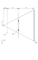
次に、図4を参照して、位置検出装置100における光路について説明する。図4は、位置検出装置100における光路の展開図であり、反射を透過のように展開した光路を示している。光源11から基準マーク22までの実効光路長としての距離L1は、1mm±0.3mmの範囲に設定される。実効光路長とは、物理長を屈折率で除した値(またはその近似値)である。基準マーク22から受光素子アレイ12bまでの実効光路長としての距離L2は、L2=L1に設定される。
Next, the optical path in the
基準マーク22には、基準マーク22の中心から数えてn番目の境界位置が、以下の式(1)で表されるXnの位置に形成されている。
The nth boundary position, counting from the center of the

本実施形態では、f=0.5mm、λ=650nmである。また、基準マーク22の幅は、中心から±128μmの領域である。
In this embodiment, f = 0.5 mm, λ = 650 nm. The width of the
或いは、別の設計例として以下の式のようにしても効果は同様である。 Alternatively, as another design example, the following formula would achieve the same effect.

32個の受光素子は、A+相、B+相、A-相、および、B-相の順に循環的に割り当てられており、これら4つの相における各相に割り当てられた8個の受光素子が1つの受光素子群を構成する。A+相の受光素子(第1受光素子)が8個あり、これらが1つの群を構成する。B+相の受光素子(第2受光素子)が8個あり、これらが1つの群を構成する。A-相の受光素子(第3受光素子)が8個あり、これらが1つの群を構成する。B-相の受光素子(第4受光素子)が8個あり、これらが1つの群を構成する。A+相の受光素子(第1受光素子)とB+相の受光素子(第2受光素子)が互いに隣接している。A-相の受光素子(第3受光素子)とB-相の受光素子(第4受光素子)の間に、A+相の受光素子(第1受光素子)とB+相の受光素子(第2受光素子)が配置されている。同一相における受光素子の周期Ppd(循環周期)は、受光素子4個分の幅に相当する256μmであり、受光素子面上の光強度分布の検出周期に相当する。 The 32 light receiving elements are cyclically assigned in the order of A+ phase, B+ phase, A- phase, and B- phase, and the eight light receiving elements assigned to each of these four phases constitute one light receiving element group. There are eight A+ phase light receiving elements (first light receiving elements), which constitute one group. There are eight B+ phase light receiving elements (second light receiving elements), which constitute one group. There are eight A- phase light receiving elements (third light receiving elements), which constitute one group. There are eight B- phase light receiving elements (fourth light receiving elements), which constitute one group. The A+ phase light receiving elements (first light receiving elements) and the B+ phase light receiving elements (second light receiving elements) are adjacent to each other. An A+-phase light receiving element (first light receiving element) and a B+-phase light receiving element (second light receiving element) are arranged between an A-phase light receiving element (third light receiving element) and a B-phase light receiving element (fourth light receiving element). The period P pd (circulation period) of the light receiving elements in the same phase is 256 μm, which corresponds to the width of four light receiving elements, and corresponds to the detection period of the light intensity distribution on the light receiving element surface.
各受光素子群を構成する8つの受光素子は、互いに電気的に接続されており、これらの出力(電流)は互いに足し合わされて後段に相ごとに設けられたIV変換アンプ(不図示)に入力される。4つのIV変換アンプは、互いに位相が異なる4相の信号S1(A+)、S1(B+)、S1(A-)、および、S1(B-)をそれぞれ出力する。信号S1(A+)、S1(B+)、S1(A-)、S1(B-)は、スケール20の移動に応じてその値が正弦波状に変化する電圧信号(正弦波信号)となる。4つの相に対して設けられた4つのIVアンプの出力信号は、信号位相の0度、90度、180度、および、270度にそれぞれ対応している。つまり、第1受光素子からの信号と第3受光素子からの信号との位相は180度異なり、第2の受光素子からの信号と第4光素子からの信号との位相は180度異なる。
The eight light receiving elements constituting each light receiving element group are electrically connected to each other, and their outputs (currents) are added together and input to an IV conversion amplifier (not shown) provided for each phase in the subsequent stage. The four IV conversion amplifiers output four-phase signals S1 (A+), S1 (B+), S1 (A-), and S1 (B-), each of which has a different phase from each other. The signals S1 (A+), S1 (B+), S1 (A-), and S1 (B-) are voltage signals (sine wave signals) whose values change sinusoidally according to the movement of the
さらに、4相の信号S1(A+)、S1(B+)、S1(A-)、S1(B-)に対して、以下の式(3)、(4)で表される演算を行い、4相の信号から直流成分が除去された2相の正弦波信号S1(A)、S1(B)に変換する。 Furthermore, the four-phase signals S1(A+), S1(B+), S1(A-), and S1(B-) are subjected to the calculations expressed by the following equations (3) and (4), and converted into two-phase sine wave signals S1(A) and S1(B) with the DC components removed from the four-phase signals.
S1(A)=S1(A+)-S1(A-) …(3)
S1(B)=S1(B+)-S1(B-) …(4)
受光IC13aから出力された2相の正弦波信号S1(A)、S1(B)は、信号処理回路101に送られる。信号処理回路101のインクリメント処理部102は、以下の式(5)で表される演算により、位置信号の元となる位相信号Φ1を取得する。
S1(A)=S1(A+)-S1(A-) ... (3)
S1(B)=S1(B+)-S1(B-) ... (4)
The two-phase sine wave signals S1(A) and S1(B) output from the
Φ1=ATAN2[S1(A),S1(B)] …(5)
式(5)において、ATAN2[Y,X]は、象限を判別して0~2π位相に変換する逆正接演算関数である。さらに、インクリメント処理部102は位相信号Φ1の変化量を累積することで位置情報を生成する。
Φ1=ATAN2[S1(A), S1(B)] ... (5)
In equation (5), ATAN2[Y,X] is an arctangent calculation function that distinguishes the quadrant and converts it into a phase of 0 to 2π. Furthermore, the
次に、図6を参照して、受光IC13bにおける受光素子アレイ12b(受光部)の配列について説明する。図6は、受光素子アレイ12bの平面図であり、受光素子アレイ12bの受光面の配列をそれぞれ示している。受光素子アレイ12bにおいて、複数(32個)の受光素子がX方向に沿って一列に配列されている。受光素子アレイ12bは、B-相の信号を出力する第1受光素子と、A+相の信号を出力する第2受光素子と、B+相の信号を出力する第3受光素子と、A-相の信号を出力する第4受光素子と、を有する。受光素子アレイ12bでは、第1受光素子、第2受光素子、第3受光素子、第4受光素子の順に配列されている。1個の受光素子に関し、X方向の幅Xpdは64μm、X方向に対して直交する方向(Y方向)の幅Ypdは450μmである。受光素子アレイ12bのX方向の全体幅Wpdは2048μmである。
Next, the arrangement of the light
32個の受光素子のうち、中央の8つの受光素子がB-相、B-相、A+相、A+相、B+相、B+相、A-相、A-相の順に割り当てられている。互いに隣接する2つの同一相の受光素子が1つの受光素子群を構成する。各受光素子群を構成する2つの受光素子は、互いに電気的に接続されており、これらの出力(電流)は互いに足し合わされて後段に相ごとに設けられたIV変換アンプ(不図示)に入力される。4つのIV変換アンプは、互いに位相が異なる4相の信号S2(A+)、S2(B+)、S2(A-)、および、S2(B-)をそれぞれ出力する。 Of the 32 light receiving elements, the eight central light receiving elements are assigned in the order of B-phase, B-phase, A+phase, A+phase, B+phase, B+phase, A-phase, and A-phase. Two adjacent light receiving elements of the same phase form one light receiving element group. The two light receiving elements that form each light receiving element group are electrically connected to each other, and their outputs (currents) are added together and input to an IV conversion amplifier (not shown) provided for each phase in the subsequent stage. The four IV conversion amplifiers each output four-phase signals S2 (A+), S2 (B+), S2 (A-), and S2 (B-) that are out of phase with each other.
さらに、受光IC13bでは、4相の信号S2(A+)、S2(B+)、S2(A-)、S2(B-)に対して、以下の式(6)、(7)で表される減算を行い、2相の、差分の信号S2(A)、S2(B)に変換する。受光IC13bから出力された2相の信号S2(A)、S2(B)は、信号処理回路101の基準位置検出処理部103に送られる。
Furthermore, the
S2(A)=S2(A+)-S2(A-) …(6)
S2(B)=S2(B+)-S2(B-) …(7)
基準位置マーク22の回折によって生じる影の中心からの距離Dは、以下の式8で計算できる。ここで、距離Z1は光源11から前記スケール20までの距離(本実施例ではL1)、距離Z2はスケール20から受光素子アレイ12bの面までの距離(本実施形態ではL2)である。wは基準位置マーク22の幅、である。
S2(A)=S2(A+)-S2(A-) ... (6)
S2(B)=S2(B+)-S2(B-) ... (7)
The distance D from the center of the shadow generated by diffraction of the
D=(Z1+Z2)/Z1×(w/2) …(8)
本実施例における、基準マーク22の回折によって生じる影の幅は、基準マーク22の2倍拡大像となり、中心から±256μmとなる。一方、減算に用いられる受光素子(図6のA-およびB-)は、中心から-256~-128μmの範囲と+128~+256μmとなる。つまり、A-相の受光素子とB-相の受光素子は、受光素子の中心からの距離Xが、X<(Z1+Z2)/Z1×(w/2)を満たす位置に配置されている。このように、回折レンズ構造の影となる領域を含む位置に配置された受光素子を減算に用いることで、基準マーク22付近の信号振幅を増大させることが可能となる。それにより、誤検出しにくい基準位置検出が実現できる。
D = (Z1 + Z2) / Z1 × (w / 2) ... (8)
In this embodiment, the width of the shadow caused by the diffraction of the
次に、図7を参照して、信号処理回路101の基準位置検出処理部103を説明する。図7は、基準位置検出処理部103と受光IC13bのブロック図である。基準位置検出処理部103は、2相の信号S2(A)、S2(B)に対して、以下の式(9)、(10)で表される演算を行い、差動信号Zsubと加算信号Zaddを取得する。
Next, the reference position
Zsub=S2(A)-S2(B) …(9)
Zadd=S2(A)+S2(B) …(10)
差動信号Zsub、加算信号Zaddは、ともに基準電圧Vrefを基準に出力するようにオフセットを加えている。加算信号Zaddは、比較器に入力され、下記式(11)の条件にてハイレベルとなる2値化出力をゲート信号Zgateとして生成する。
Zsub = S2(A) - S2(B) ... (9)
Zadd = S2(A) + S2(B) ... (10)
An offset is added to both the differential signal Zsub and the sum signal Zadd so that they are output based on the reference voltage Vref. The sum signal Zadd is input to a comparator, which generates a binary output that becomes high level under the condition of the following equation (11) as the gate signal Zgate.
Zadd>Th2 …(11)
ここでTh2は、比較器の2値化閾値レベルであり、基準マーク22の近傍でのみハイレベルを出力するように、あらかじめ設定されている。Zsubは、比較器に入力され、下記式(12)の条件にてハイレベルとなる2値化出力をエッジ信号として生成する。
Zadd>Th2 ... (11)
Here, Th2 is a binary threshold level of the comparator, which is preset so as to output a high level only in the vicinity of the
Zsub>Th1 …(12)
ここで、Th1は、比較器の2値化閾値レベルであり、例えば基準電圧Vrefと同じ値を用いることができる。エッジ信号はさらに微分回路に入力し、エッジ信号の立ち上がりで所定の時間幅を持つパルス信号として、立ち上がりエッジ信号Priseを出力させる。さらに、ゲート信号Zgateと立ち上がりエッジ信号Priseを論理積回路(AND回路)に入力し、原点信号Zpulseとして出力する。
Zsub>Th1 ... (12)
Here, Th1 is a binary threshold level of the comparator, and may be the same value as the reference voltage Vref. The edge signal is further input to a differentiation circuit, which outputs a rising edge signal Prise as a pulse signal having a predetermined time width at the rising edge of the edge signal. Furthermore, the gate signal Zgate and the rising edge signal Prise are input to a logical product circuit (AND circuit), which outputs the origin signal Zpulse.
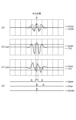
次に、図8を参照して、基準マーク22近傍での各信号波形について説明する。図8は、基準マーク22からの光を受光素子アレイ12bで検出した場合の基準マーク22近傍における信号波形図である。図8(a)は、基準マーク22の近傍での2相の信号S2(A)、S2(B)の波形を示している。図8(b)は、基準マーク22の近傍での加算信号Zaddおよび閾値Th2の波形を示している。
Next, referring to Figure 8, the signal waveforms in the vicinity of the
図8(c)は、基準マーク22の近傍での差動信号Zsub、閾値Th1の波形を示している。閾値Th1はヒステリシスを持たせてあり、比較器出力がハイになったら閾値Th1がマイナス側にオフセットするようになっている。このようにすることで、信号変化が急峻な基準マーク22の中心付近でのエッジ検出を行うとともに、それ以外の場所での不要なエッジ検出を抑えることができる。不要なエッジ検出を抑えることで、インクリメント信号へのクロストークが低減される。
Figure 8 (c) shows the waveforms of the differential signal Zsub and threshold value Th1 near the
図8(d)は、基準マーク22の近傍でのゲート信号Zgate、立ち上がりエッジ信号Prise、原点信号Zpulse(原点パルス)の波形を示している。原点信号Zpulse(原点パルス)の波形は、基準マークの中心位置(基準位置)を示しているのが分かる。本実施形態によれば、基準マークが回折レンズ構造である場合でも、基準位置を高精度に検出することが可能となる。
Figure 8 (d) shows the waveforms of the gate signal Zgate, the rising edge signal Prise, and the origin signal Zpulse (origin pulse) near the
次に、比較例として、2相の信号出力のみを用いて原点パルスを得る場合を示す。4つのIV変換アンプから出力される4相の信号S2(A+)、S2(B+)、S2(A-)、S2(B-)のうち、S2(A+)、S2(B+)だけを用いた例を説明する。比較例では、S2(A+)、S2(B+)を用いて、以下の式(13)の演算を行う。 Next, as a comparative example, a case where an origin pulse is obtained using only two-phase signal output is shown. Of the four-phase signals S2(A+), S2(B+), S2(A-), and S2(B-) output from four IV conversion amplifiers, an example is described in which only S2(A+) and S2(B+) are used. In the comparative example, the following equation (13) is calculated using S2(A+) and S2(B+).
Zadd´=S2(A+)+S2(B+) …(13)
図9を参照して、比較例における基準マーク22の近傍での各信号波形について説明する。図9は、比較例における、基準マーク22からの光を受光素子アレイ12bで検出した場合の基準マーク22近傍における信号波形図である。図9(a)は、基準マーク22の近傍での2相の信号S2(A+)、S2(B+)の波形を示している。図9(b)は、基準マーク22の近傍での加算信号Zadd´および閾値Th2の波形を示している。
Zadd' = S2(A+) + S2(B+) ... (13)
With reference to Fig. 9, the signal waveforms in the vicinity of the
図9(c)は、基準マーク22の近傍におけるゲート信号Zgateの波形を示している。加算信号Zadd´における基準マーク22の中心位置付近の信号901の値は、基準マーク22から離れた反射部23の位置における信号902の値と同等程度となっている。そのため、ゲート信号Zgateから基準マークの中心位置を高精度に求めることはできない。これは、基準マーク22の回折レンズ構造によって、集光位置以外の周辺部で光量が低下していることが原因であり、信号S2(A+)、S2(B+)のみを用いるだけでは不十分であることが分かる。
Figure 9(c) shows the waveform of the gate signal Zgate near the
基準マーク22の回折によって生じる影の幅は、基準マーク22の2倍拡大像となっているため、本実施形態では、A-およびB-の受光素子からの信号S2(A-)、S2(B-)を用いる。これにより、基準マークの基準位置を高精度に検出することが可能となる。つまり、回折レンズ構造の影となる領域を含む位置に配置された受光素子を減算に用いることで、基準マーク22付近の信号振幅を増大させることが可能となる。それにより、誤検出しにくい基準位置検出が実現できる。基準位置が高精度に検出されると、スケールトラック21aを用いて式5より求められる相対位置と組み合わせて、高精度にスケール(物体)の位置を求めることができる。
Since the width of the shadow generated by the diffraction of the
(第2実施形態)
図10は、第2実施形態における位置検出装置200の構成図である。第1実施形態と異なる点は、センサユニット10内の光源11からの光が光源格子14を透過したのち、スケールトラック21bに照射される点である。
Second Embodiment
10 is a configuration diagram of a
図11を参照して、位置検出装置200における光路について説明する。図11は、位置検出装置200における光路の展開図であり、反射を透過のように展開した光路を示している。光源11から光源格子14までの実効光路長としての距離L0は0.3mmである。光源格子14から基準マーク22までの実効光路長としての距離L3は、0.7mm±0.3mmの範囲に設定される。基準マーク22から受光素子アレイ12bまでの実効光路長としての距離L4は、L4=L0+L2に設定される。
The optical path in the
基準マーク22には、基準マーク22の中心から数えてn番目の境界位置が、式(1)で表されるXnの位置に形成されている。本実施形態における回折レンズの焦点距離は、f=0.7mmである。すなわち、光源11からの発散光束は、受光素子アレイ面よりも遠い位置に収束するようになっている。こうすることで、光源格子14の周期像を受光面上に形成し、信号が不安定になるのを防ぐ効果が得られる。
The nth boundary position counted from the center of the
(第3実施形態)
図12は、第3実施形態における位置検出装置300の構成図である。第2の実施形態とは、スケールトラック21bから受光素子アレイ12bに至る光路中に原点検出格子19が設けられている点と、スケールトラック21b及び受光ICの構成、が異なる。原点検出格子19は、X方向に垂直な方向に交互に配列された透過部と遮光部とにより構成された透過型回折格子である。
Third Embodiment
12 is a configuration diagram of a
次に、図13を参照して、本実施形態におけるスケール20におけるスケールトラック21a、21bの構成について説明する。図13は、スケール20(スケールトラック21a、21b)の一部を拡大した平面図である。図13において、ドットで塗られた部分は段差パターンの凹部を示す。スケールトラック21aは、移動方向(X方向)において、周期すなわちピッチ(=4μm)ごとに、2μm幅の段差パターンが配置されたパターン列からなる。
Next, the configuration of the scale tracks 21a, 21b of the
スケールトラック21aと並行して配置されているスケールトラック21bには、スケール20上の特定の位置(基準位置)で、凹部が移動方向(X方向)において不等間隔で配置された基準マーク22(基準位置格子)が形成されている。格子間隔は基準マーク22の中心から離れるに従って小さくなっており、光源11からの発散光束が、回折によって所定の距離で線状に収束する回折レンズ構造となっている。スケールトラック21bの基準マーク22以外の領域には、移動方向(X方向)において、周期すなわちピッチ(=4.9μm)ごとに、2.45μm幅の段差パターンが配置されたパターン列からなる格子領域24(第2回折格子)が形成されている。格子領域24の格子周期は、同じ点からの+1次回折光と-1次回折光が、概略逆相(256μm)の位置に分かれて入射するように設定されている。このようにすることで、スケール上に付着するゴミや、パターン欠陥の影響が、以下の演算によってキャンセルされ、誤検出しにくくなる。
The
次に、図14を参照して、センサユニット10の構成について説明する。図14は、センサユニット10の平面図であり、センサユニット10をスケール20側から見た図を示している。光源格子14の格子パターン14aのピッチ(パターン周期)は4μmである。インクリメント検出格子15には、X方向において所定のピッチ(=4.069952μm)を有する格子パターン15が設けられている。原点検出格子19には、X方向に対して垂直な方向(Y方向)において、18μm幅の遮光部と2μm幅の開口部が交互に並べられている。この格子構造により、受光素子アレイ12bで受光する光量を減衰し、インクリメント信号との光量比を調整することができる。格子周期方向を位置検出方向に対して垂直な方向にすることで、移動方向の光量プロファイルには影響を与えないようにできる。
Next, the configuration of the
光源11から光源格子14までの実効光路長としての距離L0は0.3mmである。光源格子14から基準マーク22までの実効光路長としての距離L3は、1.6mm±0.3mmの範囲に設定される。基準マーク22から受光素子アレイ12bまでの実効光路長としての距離L4は、L4=L0+L3に設定される。
The distance L0, which is the effective optical path length from the
次に、図15を参照して、本実施形態の受光IC13aにおける受光素子アレイ12aの配列について説明する。図15は、本実施形態の受光素子アレイ12aの平面図であり、受光素子アレイ12aの受光面の配列をそれぞれ示している。受光素子アレイ12aは、複数(64個)の受光素子がX方向に沿って一列に配列されている。1個の受光素子に関し、X方向の幅Xpdは32μm、Y方向の幅Ypdは450μmである。受光素子アレイ12aのX方向の全体幅Wpdは2048μmである。
Next, the arrangement of the light
64個の受光素子は、A+相、B+相、A-相、および、B-相の順に、一部、間をとばして循環的に割り当てられており、これら4つの相のそれぞれにおいて、12個の受光素子が1つの受光素子群を構成する。同一相の受光素子の周期Ppd(循環周期)は、受光素子8個分の幅に相当する256μmであり、受光素子面上の光強度分布の検出周期に相当する。各受光素子群を構成する12個の受光素子は、互いに電気的に接続されており、これらの出力(電流)は互いに足し合わされて後段に相ごとに設けられたIV変換アンプ(不図示)に入力される。4つのIV変換アンプは、4相の信号S1(A+)、S1(B+)、S1(A-)、および、S1(B-)をそれぞれ出力する。 The 64 light receiving elements are cyclically assigned in the order of A+ phase, B+ phase, A- phase, and B- phase, skipping some gaps, and 12 light receiving elements form one light receiving element group in each of these four phases. The period P pd (cyclic period) of the light receiving elements of the same phase is 256 μm, which corresponds to the width of eight light receiving elements, and corresponds to the detection period of the light intensity distribution on the light receiving element surface. The 12 light receiving elements that form each light receiving element group are electrically connected to each other, and their outputs (currents) are added together and input to an IV conversion amplifier (not shown) provided for each phase in the subsequent stage. The four IV conversion amplifiers output four-phase signals S1 (A+), S1 (B+), S1 (A-), and S1 (B-), respectively.
信号S1(A+)、S1(B+)、S1(A-)、S1(B-)は、スケール20の移動に応じてその値が正弦波状に変化する電圧信号(正弦波信号)となる。4つの相に対して設けられた4つのIVアンプの出力信号は、信号位相の0度、90度、180度、および、270度にそれぞれ対応している。さらに、4相の信号S1(A+)、S1(B+)、S1(A-)、S1(B-)に対して、式(3)、(4)で表される演算を行い、4相の信号から直流成分が除去された2相の正弦波信号S1(A)、S1(B)に変換する。
Signals S1(A+), S1(B+), S1(A-), and S1(B-) are voltage signals (sine wave signals) whose values change sinusoidally in response to the movement of
センサユニット10から出力された2相の正弦波信号S1(A)、S1(B)は、信号処理回路101に送られる。信号処理回路101のインクリメント処理部102は、式(5)で表される演算により、位置信号の元となる位相信号Φ1を取得する。さらに、インクリメント処理部102は位相信号Φ1の変化量を累積することで位置情報を生成する。
The two-phase sine wave signals S1(A) and S1(B) output from the
受光IC13bにおける受光素子アレイ12bの配列を図16に示す。受光素子アレイ12bでは、複数(32個)の受光素子がX方向に沿って一列に配列されている。1個の受光素子に関し、X方向の幅Xpdは32μm、Y方向の幅Ypdは450μmである。受光素子アレイ12bのX方向の全体幅Wpdは2048μmである。
The arrangement of the light
64個の受光素子は、A+相、B+相、A-相、および、B-相の順に、一部間をとばして循環的に割り当てられており、これら4つの相のそれぞれにおいて、12個の受光素子が1つの受光素子群を構成する。A+相の受光素子は、中央部に8個、周辺部の左側に4個あり、これらが1つの群を構成する。B+相の受光素子は中央部に8個、周辺部の右側に4個あり、これらが1つの群を構成する。A-相の受光素子は、中央部に8個、周辺部の右側に4個あり、これらが1つの群を構成する。B-相の受光素子は中央部に8個、周辺部の左側に4個あり、これらが1つの群を構成する。中央部において、A+相の受光素子とB+相の受光素子が互いに隣接している。A-相の受光素子とB-相の受光素子の間に、A+相の受光素子とB+相の受光素子が配置されている。この周期Ppd(循環周期)は、受光素子32個分の幅に相当する1024μmである。 The 64 light receiving elements are cyclically assigned in the order of A+ phase, B+ phase, A- phase, and B- phase, skipping some spaces, and in each of these four phases, 12 light receiving elements form one light receiving element group. There are eight A+ phase light receiving elements in the center and four on the left side of the periphery, which form one group. There are eight B+ phase light receiving elements in the center and four on the right side of the periphery, which form one group. There are eight A- phase light receiving elements in the center and four on the right side of the periphery, which form one group. There are eight B- phase light receiving elements in the center and four on the left side of the periphery, which form one group. In the center, the A+ phase light receiving elements and the B+ phase light receiving elements are adjacent to each other. The A+ phase light receiving elements and the B+ phase light receiving elements are arranged between the A- phase light receiving elements and the B- phase light receiving elements. This period P pd (circulation period) is 1024 μm, which corresponds to the width of 32 light receiving elements.
受光素子アレイ12bは、中央部の各8個の受光素子4群と、その両側に、中央部の受光素子と出力を足し合わせる複数の受光素子91を有している。各受光素子群を構成する12個の受光素子は、互いに電気的に接続されており、これらの出力(電流)は互いに足し合わされて後段に相ごとに設けられたIV変換アンプ(不図示)に入力される。4つのIV変換アンプは、4相の信号S2(A+)、S2(B+)、S2(A-)、および、S2(B-)をそれぞれ出力する。中央部のA+相の受光素子(第1受光素子)の出力と足し合わされる、受光素子アレイ12bは周辺部のA+相の受光素子(第5受光素子)を有する。周辺部のA+相の受光素子は、中央部のA+相の受光素子とB+相の受光素子との隣接部(中心)からの距離が、中央部のA-相の受光素子(第3受光素子)よりも遠い位置に配置されている。
The light
さらに、4相の信号S2(A+)、S2(B+)、S2(A-)、S2(B-)に対して、式(6)、(7)で表される演算を行い、2相の信号S2(A)、S2(B)に変換する。受光IC13bから出力された2相の信号S2(A)、S2(B)は、信号処理回路101の基準位置検出処理部103に送られる。
Furthermore, the four-phase signals S2(A+), S2(B+), S2(A-), and S2(B-) are converted into two-phase signals S2(A) and S2(B) by performing the calculations expressed by equations (6) and (7). The two-phase signals S2(A) and S2(B) output from the
基準マーク22の回折によって生じる影の中心からの距離Dは、以下の式14で計算できる。
The distance D from the center of the shadow caused by diffraction of the
D=(Z1+Z2)/Z1×(w/2+Z2×tan(arcsin(λ/d))) …(14)
ここで、Z1は光源11からスケール20までの距離(本実施形態ではL0+L3)、Z2はスケール20から受光素子アレイ12bの面までの距離(本実施形態ではL4)である。λは光源11の波長、dは格子領域24の格子間隔、wは基準マーク22の幅である。
D = (Z1 + Z2) / Z1 × (w / 2 + Z2 × tan (arcsin (λ / d))) ... (14)
Here, Z1 is the distance from the
本実施形態では、減算に用いられる受光素子(図16のA-およびB-)の少なくとも一部が、距離Dの範囲の内側に配置されている。つまり、A-相の受光素子とB-相の受光素子は、受光素子の中心からの距離Xが、X<(Z1+Z2)/Z1×(w/2+Z2×tan(arcsin(λ/d)))を満たす位置に配置されている。このように、回折レンズ構造の影となる領域を含む位置に配置された受光素子を減算に用いることで、基準マーク22付近の信号振幅を増大させることが可能となる。それにより、誤検出しにくい基準位置検出が実現できる。
In this embodiment, at least some of the light receiving elements (A- and B- in FIG. 16) used for subtraction are arranged inside the range of distance D. In other words, the A-phase light receiving element and the B-phase light receiving element are arranged at positions where the distance X from the center of the light receiving element satisfies X<(Z1+Z2)/Z1×(w/2+Z2×tan(arcsin(λ/d))). In this way, by using light receiving elements arranged at positions including the area shaded by the diffractive lens structure for subtraction, it is possible to increase the signal amplitude near the
次に、図17を参照して、基準マーク22の近傍での各信号波形について説明する。図17は、基準マーク22からの光を受光素子アレイ12bで検出した場合の基準マーク22近傍における信号波形図である。図17(a)は、基準マーク22の近傍での2相の信号S2(A)、S2(B)の波形を示している。図17(b)は、基準マーク22の近傍での加算信号Zaddおよび閾値Th2の波形を示している。図17(c)は、基準マーク22の近傍での差動信号Zsub、閾値Th1の波形を示している。図17(d)は、基準マーク22の近傍でのゲート信号Zgate、立ち上がりエッジ信号Prise、原点信号Zpulse(原点パルス)の波形を示している。原点信号Zpulse(原点パルス)の波形は、基準マークの中心位置を示しているのが分かる。本実施形態によれば、基準マークが回折レンズ構造である場合でも、基準位置を高精度に検出することが可能となる。
Next, referring to FIG. 17, the signal waveforms in the vicinity of the
(第4実施形態)
図18を参照して、第4実施形態におけるスケール20におけるスケールトラック21a、21bの構成について説明する。図18は、スケール20(スケールトラック21a、21b)の一部を拡大した平面図である。図17において、ドットで塗られた部分は段差パターンの凹部を示す。スケールトラック21aは、移動方向(X方向)において、周期4μmごとに、2μm幅の段差パターンが配置されたパターン列からなる。また、スケールトラック21aと並行して配置されているスケールトラック21bには、スケール20上の特定の位置(基準位置)で、凹部がX方向において不等間隔で配置された基準マーク22(基準格子)が形成されている。格子間隔は基準マーク22の中心から離れるに従って小さくなっており、光源11からの発散光束が、回折によって所定の距離で線状に収束する回折レンズ構造となっている。スケールトラック21bの基準マーク22以外の領域には、X方向において、周期4.9μmごとに、2.45μm幅の段差パターンが配置されたパターン列からなる格子領域24(第2回折格子)が形成されている。パターン列からなる格子領域24は、間隔を置いて複数配列されている。基準マーク22の中心から両側に384~512μmの範囲、および、640~768μmの範囲には、格子の無い領域25(反射部)がある。
Fourth Embodiment
The configuration of the scale tracks 21a and 21b in the
受光素子12bの配置は第3実施形態のものと同じである。基準マーク22の中心から384~512μmの範囲からの反射光は、複数の受光素子91のプラス側(図16の受光素子91のA+、B+)に入射する。このようにすることで、原点位置でのZadd信号を増大することができ、誤検出を防止することができる。
The arrangement of the
次に、図19を参照して、基準マーク22の近傍での各信号波形について説明する。図19は、基準マーク22の近傍での信号波形図である。図19(a)は、基準マーク22の近傍での2相の信号S2(A)、S2(B)の波形を示している。図19(b)は、基準マーク22の近傍での加算信号Zaddおよび閾値Th2の波形を示している。図19(c)は、基準マーク22の近傍での差動信号Zsub、閾値Th1の波形を示している。図19(d)は、基準マーク22の近傍でのゲート信号Zgate、立ち上がりエッジ信号Prise、原点信号Zpulse(原点パルス)の波形を示している。原点信号Zpulse(原点パルス)の波形は、基準マークの中心位置を示しているのが分かる。本実施形態によれば、基準マークが回折レンズ構造である場合でも、基準位置を高精度に検出することが可能となる。
Next, referring to FIG. 19, the signal waveforms in the vicinity of the
なお、上述の実施形態では、光源からの光を反射型スケール(スケール格子)にて反射して受光素子アレイで受光する反射型の位置検出装置について説明したが、これに限定されるものではない。各実施形態は、例えば、光源からの光に対して透過型スケールを透過させて受光素子アレイで受光する透過型の位置検出装置にも適用可能である。また、各実施形態において、リニアスケールを用いた位置検出装置(リニアエンコーダ)について説明したが、これに限定されるものではない。各実施形態は、例えばロータリースケールを用いたロータリーエンコーダにも適用可能である。ロータリーエンコーダの場合、スケールパターンを放射状に構成すればよい。なお、上述の実施形態では、スケール20のパターンを段差による位相パターンとしているが、それに限るものではない。同一の設計で、凹部、凸部の代わりに、反射、非反射によるパターンとしても同様の効果が得られる。
In the above-mentioned embodiment, a reflective position detection device is described in which light from a light source is reflected by a reflective scale (scale grating) and received by a light receiving element array, but the present invention is not limited to this. Each embodiment can also be applied to a transmissive position detection device in which light from a light source is transmitted through a transmissive scale and received by a light receiving element array. In addition, each embodiment describes a position detection device (linear encoder) using a linear scale, but the present invention is not limited to this. Each embodiment can also be applied to a rotary encoder using a rotary scale, for example. In the case of a rotary encoder, the scale pattern may be configured radially. In the above-mentioned embodiment, the pattern of the
(第5実施形態)
次に、図20を参照して、第5実施形態における露光装置について説明する。図20は、本実施形態における露光装置400の概略構成図である。露光装置400は、半導体ウエハに電子回路を露光するように構成され、例えば第1実施形態にて説明した位置検出装置100を搭載している。露光装置400は、位置検出装置100を用いて、半導体ウエハが搭載されて2次元方向に駆動可能なステージの位置を検出する。
Fifth Embodiment
Next, an exposure apparatus in the fifth embodiment will be described with reference to Fig. 20. Fig. 20 is a schematic configuration diagram of an
図20において、露光装置400は、動作可能な可動部としてのステージ50と、ウエハ53に対して不図示のマスクの光学像である電子回路像を投影(露光)する投影光学系51を有する。ステージ50上にはウエハ53が搭載されている。ステージ50は、駆動機構55によって、投影光学系51に対してX方向およびY方向に駆動される。これにより、ウエハ53上における電子回路像の投影位置が制御される。
In FIG. 20, the
露光装置400は位置検出装置100を有する。位置検出装置100のスケール20は、ステージ50(可動部)に取り付けられている。位置検出装置100のセンサユニット10は、露光装置400の固定部である筐体54に取り付けられている。なお、本実施形態において、固定部と可動部の関係は逆でもよく、センサユニット10を可動部に取り付け、スケール20を固定部に取り付けることができる。すなわち、センサユニット10とスケール20とが相対的に移動可能であればよい。また、本実施形態において、位置検出装置100(センサユニット10)に代えて、第2~4の実施形態における位置検出装置を用いてもよい。
The
露光装置400は位置検出装置100の検出結果、つまり、センサユニット10の受光素子アレイ12a、12bからの出力信号に基づいてステージ50の位置を演算し、駆動機構55を制御する制御部56を有する。
The
位置検出装置によって高精度に基準位置を検出することにより、露光装置200のステージ50の位置を高分解能かつ安定的に検出し、ステージ50の移動(動作)を高精度に制御することができる。
By detecting the reference position with high accuracy using the position detection device, the position of the
(第6実施形態)
図21は、ガルバノ走査装置(ガルバノスキャナ)を含むレーザー加工装置の例を示す図である。レーザー加工装置は、レーザー光源610と、ガルバノ走査装置620、630と、レンズ640を有する。レーザー光源610からのレーザー光を、ガルバノ走査装置620、630で、直交する2軸方向に偏向させる。レンズ640で集光されたレーザー光は、加工対象物650に照射される。
Sixth Embodiment
21 is a diagram showing an example of a laser processing apparatus including a galvanometer scanner. The laser processing apparatus has a
ガルバノ走査装置620、630は回転可動部にミラーを備え、モータにより駆動される。ガルバノ走査装置620、630は、モータ及びミラーの回転軸に取り付けられた、上述の光学式エンコーダ(ロータリーエンコーダ)を有する。光学式エンコーダの出力を、CPU等の演算装置を内蔵した不図示の制御部に入力し、制御部はモータの回転角度制御を行う。上述のエンコーダを用いることで高精度に位置(回転角)を検出することができ、モータの回転角を高精度に制御することができる。
The
なお、駆動制御装置における可動部としては第5実施形態や第6実施形態のようなステージやミラーに限られず、駆動変位可能なものであれば適用可能である。即ち、上述の光学式エンコーダを用いて可動部の変位量を測定し、測定された変位量に基づき前記可動部の動作を制御する駆動制御装置全般に適用できる。例えば、ロボットアームまたは組み立て対象物を搬送する搬送体を備えた工作機器と、この工作機器の位置または姿勢を検出する各実施形態のエンコーダとを有する工作装置を構成することにより、搬送体の位置を高精度に検出することができる。 The movable part in the drive control device is not limited to a stage or mirror as in the fifth and sixth embodiments, and can be anything that can be driven and displaced. In other words, the above-mentioned optical encoder can be used to measure the amount of displacement of a movable part, and the drive control device can be generally applied to control the operation of the movable part based on the measured amount of displacement. For example, by configuring a machine tool having a robot arm or a carrier for carrying an assembly object, and an encoder of each embodiment that detects the position or attitude of the machine tool, the position of the carrier can be detected with high accuracy.
以上、本発明の好ましい実施例について説明したが、本発明はこれらの実施例に限定されず、その要旨の範囲内で種々の変形及び変更が可能である。 The above describes preferred embodiments of the present invention, but the present invention is not limited to these embodiments, and various modifications and variations are possible within the scope of the gist of the invention.
Claims (13)
前記スケールは、基準位置を検出するための、格子の周期方向に回折光を集光する回折格子を有し、
前記受光素子は、前記回折格子からの光を受光する受光素子アレイを有し、
前記受光素子アレイは、位相が互いに異なる信号を出力する、第1受光素子と第2受光素子と第3受光素子と第4受光素子を有し、
前記第1受光素子と前記第2受光素子が隣接し、前記第3受光素子と前記第4受光素子の間に前記第1受光素子と前記第2受光素子が配置され、
前記処理部は、前記第1受光素子からの信号と前記第3受光素子からの信号の差分である第1差分信号、及び、前記第2受光素子からの信号と前記第4受光素子からの信号の差分である第2差分信号を取得し、前記第1差分信号と前記第2差分信号の差分の信号と加算の信号、に基づいて、前記基準位置を表す信号を生成し、
前記回折格子は、中心から離れるほど格子周期が小さくなる第1回折格子と、前記第1回折格子の周辺に形成された、前記第1回折格子とは異なる第2回折格子と、を有することを特徴とする光学式エンコーダ。 An optical encoder having a light source, a scale, a light receiving element that receives light from the scale, and a processing unit that processes a signal from the light receiving element,
the scale has a diffraction grating for detecting a reference position, the diffraction grating focusing diffracted light in a grating period direction;
the light receiving element has a light receiving element array that receives light from the diffraction grating,
the light receiving element array includes a first light receiving element, a second light receiving element, a third light receiving element, and a fourth light receiving element which output signals having different phases from each other;
the first light receiving element and the second light receiving element are adjacent to each other, and the first light receiving element and the second light receiving element are disposed between the third light receiving element and the fourth light receiving element;
the processing unit acquires a first differential signal which is a difference between a signal from the first light receiving element and a signal from the third light receiving element, and a second differential signal which is a difference between a signal from the second light receiving element and a signal from the fourth light receiving element, and generates a signal representing the reference position based on a signal of the difference between the first differential signal and the second differential signal and an added signal;
An optical encoder characterized in that the diffraction grating has a first diffraction grating whose grating period becomes smaller the further away from the center, and a second diffraction grating different from the first diffraction grating and formed around the first diffraction grating .
前記第1受光素子と前記第2受光素子との隣接部からの距離が、前記第3受光素子よりも遠い位置に前記第5受光素子が配置されていることを特徴とする請求項1に記載の光学式エンコーダ。 the light receiving element array has a fifth light receiving element whose output is added to the output of the first light receiving element;
2. The optical encoder according to claim 1, wherein the fifth light receiving element is disposed at a position farther from an adjacent portion of the first light receiving element and the second light receiving element than the third light receiving element.
前記スケールは、基準位置を検出するための、格子の周期方向に回折光を集光する回折格子を有し、
前記受光素子は、前記回折格子からの光を受光する受光素子アレイを有し、
前記受光素子アレイは、位相が互いに異なる信号を出力する、第1受光素子と第2受光素子と第3受光素子と第4受光素子を有し、
前記第1受光素子と前記第2受光素子が隣接し、前記第3受光素子と前記第4受光素子の間に前記第1受光素子と前記第2受光素子が配置され、
前記処理部は、前記第1受光素子からの信号と前記第3受光素子からの信号の差分である第1差分信号、及び、前記第2受光素子からの信号と前記第4受光素子からの信号の差分である第2差分信号を取得し、前記第1差分信号と前記第2差分信号の差分の信号と加算の信号、に基づいて、前記基準位置を表す信号を生成し、
前記回折格子は、中心から離れるほど格子周期が小さくなる第1回折格子を有し、
前記光源から前記スケールまでの距離をZ1、前記スケールから前記受光素子アレイの面までの距離をZ2、前記第1回折格子の幅をw、とし、
前記第3受光素子及び前記第4受光素子は、前記受光素子アレイの中心からの距離Xが、X<(Z1+Z2)/Z1×(w/2)を満たす位置に配置されていることを特徴とする光学式エンコーダ。 An optical encoder having a light source, a scale, a light receiving element that receives light from the scale, and a processing unit that processes a signal from the light receiving element,
the scale has a diffraction grating for detecting a reference position, the diffraction grating focusing diffracted light in a grating period direction;
the light receiving element has a light receiving element array that receives light from the diffraction grating,
the light receiving element array includes a first light receiving element, a second light receiving element, a third light receiving element, and a fourth light receiving element which output signals having different phases from each other;
the first light receiving element and the second light receiving element are adjacent to each other, and the first light receiving element and the second light receiving element are disposed between the third light receiving element and the fourth light receiving element;
the processing unit acquires a first differential signal which is a difference between a signal from the first light receiving element and a signal from the third light receiving element, and a second differential signal which is a difference between a signal from the second light receiving element and a signal from the fourth light receiving element, and generates a signal representing the reference position based on a signal of the difference between the first differential signal and the second differential signal and an added signal;
the diffraction grating has a first diffraction grating whose grating period decreases with increasing distance from the center,
The distance from the light source to the scale is Z1, the distance from the scale to the surface of the light receiving element array is Z2, and the width of the first diffraction grating is w,
the third light receiving element and the fourth light receiving element are arranged at positions where a distance X from a center of the light receiving element array satisfies X<(Z1+Z2)/Z1×(w/2).
前記回折格子の幅をw、とし、
前記第3受光素子及び前記第4受光素子は、前記受光素子アレイの中心からの距離Xが、X<(Z1+Z2)/Z1×(w/2+Z2×tan(arcsin(λ/d)))を満たす位置に配置されていることを特徴とする請求項1に記載の光学式エンコーダ。 The distance from the light source to the scale is Z1, the distance from the scale to the surface of the light receiving element array is Z2, the wavelength of the light source is λ, and the period of the second diffraction grating is d.
The width of the diffraction grating is w,
2. The optical encoder according to claim 1, wherein the third light receiving element and the fourth light receiving element are arranged at positions where a distance X from a center of the light receiving element array satisfies X<(Z1+Z2)/Z1×(w/2+Z2×tan(arcsin(λ/d))).
前記スケールは、基準位置を検出するための、格子の周期方向に回折光を集光する回折格子を有し、
前記受光素子は、前記回折格子からの光を受光する受光素子アレイを有し、
前記受光素子アレイは、位相が互いに異なる信号を出力する、第1受光素子と第2受光素子と第3受光素子と第4受光素子を有し、
前記第1受光素子と前記第2受光素子が隣接し、前記第3受光素子と前記第4受光素子の間に前記第1受光素子と前記第2受光素子が配置され、
前記処理部は、前記第1受光素子からの信号と前記第3受光素子からの信号の差分である第1差分信号、及び、前記第2受光素子からの信号と前記第4受光素子からの信号の差分である第2差分信号を取得し、前記第1差分信号と前記第2差分信号の差分の信号と加算の信号、に基づいて、前記基準位置を表す信号を生成し、
前記光源と前記スケールの間に配置された回折格子を有し、前記光源からの発散光束が前記受光素子アレイの面より遠い側に収束することを特徴とする光学式エンコーダ。 An optical encoder having a light source, a scale, a light receiving element that receives light from the scale, and a processing unit that processes a signal from the light receiving element,
the scale has a diffraction grating for detecting a reference position, the diffraction grating focusing diffracted light in a grating period direction;
the light receiving element has a light receiving element array that receives light from the diffraction grating,
the light receiving element array includes a first light receiving element, a second light receiving element, a third light receiving element, and a fourth light receiving element which output signals having different phases from each other;
the first light receiving element and the second light receiving element are adjacent to each other, and the first light receiving element and the second light receiving element are disposed between the third light receiving element and the fourth light receiving element;
the processing unit acquires a first differential signal which is a difference between a signal from the first light receiving element and a signal from the third light receiving element, and a second differential signal which is a difference between a signal from the second light receiving element and a signal from the fourth light receiving element, and generates a signal representing the reference position based on a signal of the difference between the first differential signal and the second differential signal and an added signal;
An optical encoder comprising: a diffraction grating disposed between the light source and the scale; and a divergent light beam from the light source converging on a side farther from a surface of the light receiving element array.
前記スケールは、基準位置を検出するための、格子の周期方向に回折光を集光する回折格子を有し、
前記受光素子は、前記回折格子からの光を受光する受光素子アレイを有し、
前記受光素子アレイは、位相が互いに異なる信号を出力する、第1受光素子と第2受光素子と第3受光素子と第4受光素子を有し、
前記第1受光素子と前記第2受光素子が隣接し、前記第3受光素子と前記第4受光素子の間に前記第1受光素子と前記第2受光素子が配置され、
前記処理部は、前記第1受光素子からの信号と前記第3受光素子からの信号の差分である第1差分信号、及び、前記第2受光素子からの信号と前記第4受光素子からの信号の差分である第2差分信号を取得し、前記第1差分信号と前記第2差分信号の差分の信号と加算の信号、に基づいて、前記基準位置を表す信号を生成し、
前記回折格子は、中心から離れるほど格子周期が小さくなる第1回折格子と、前記第1回折格子の隣に、所定の間隔をおいて形成された複数の第2回折格子と、を有し、
前記複数の第2回折格子の間は回折格子の無い領域であることを特徴とする光学式エンコーダ。 An optical encoder having a light source, a scale, a light receiving element that receives light from the scale, and a processing unit that processes a signal from the light receiving element,
the scale has a diffraction grating for detecting a reference position, the diffraction grating focusing diffracted light in a grating period direction;
the light receiving element has a light receiving element array that receives light from the diffraction grating,
the light receiving element array includes a first light receiving element, a second light receiving element, a third light receiving element, and a fourth light receiving element which output signals having different phases from each other;
the first light receiving element and the second light receiving element are adjacent to each other, and the first light receiving element and the second light receiving element are disposed between the third light receiving element and the fourth light receiving element;
the processing unit acquires a first differential signal which is a difference between a signal from the first light receiving element and a signal from the third light receiving element, and a second differential signal which is a difference between a signal from the second light receiving element and a signal from the fourth light receiving element, and generates a signal representing the reference position based on a signal of the difference between the first differential signal and the second differential signal and an added signal;
the diffraction grating includes a first diffraction grating having a grating period that decreases with increasing distance from the center, and a plurality of second diffraction gratings formed adjacent to the first diffraction grating at predetermined intervals;
An optical encoder, comprising: an area between the plurality of second diffraction gratings that is free of a diffraction grating.
前記光学式エンコーダによる検出結果に基づいて物体の変位を制御する制御部と、を有することを特徴とする制御装置。 An optical encoder according to any one of claims 1 to 12 ;
and a control unit that controls the displacement of an object based on a detection result by the optical encoder.
Priority Applications (4)
| Application Number | Priority Date | Filing Date | Title |
|---|---|---|---|
| JP2020099491A JP7475973B2 (en) | 2020-06-08 | 2020-06-08 | Optical Encoder and Control Device |
| US17/337,918 US11946780B2 (en) | 2020-06-08 | 2021-06-03 | Optical encoder and control apparatus |
| DE102021114506.6A DE102021114506A1 (en) | 2020-06-08 | 2021-06-07 | Optical encoder and control unit |
| GB2108112.0A GB2596916B (en) | 2020-06-08 | 2021-06-07 | Optical encoder and control apparatus |
Applications Claiming Priority (1)
| Application Number | Priority Date | Filing Date | Title |
|---|---|---|---|
| JP2020099491A JP7475973B2 (en) | 2020-06-08 | 2020-06-08 | Optical Encoder and Control Device |
Publications (3)
| Publication Number | Publication Date |
|---|---|
| JP2021193354A JP2021193354A (en) | 2021-12-23 |
| JP2021193354A5 JP2021193354A5 (en) | 2023-06-08 |
| JP7475973B2 true JP7475973B2 (en) | 2024-04-30 |
Family
ID=76838741
Family Applications (1)
| Application Number | Title | Priority Date | Filing Date |
|---|---|---|---|
| JP2020099491A Active JP7475973B2 (en) | 2020-06-08 | 2020-06-08 | Optical Encoder and Control Device |
Country Status (4)
| Country | Link |
|---|---|
| US (1) | US11946780B2 (en) |
| JP (1) | JP7475973B2 (en) |
| DE (1) | DE102021114506A1 (en) |
| GB (1) | GB2596916B (en) |
Citations (5)
| Publication number | Priority date | Publication date | Assignee | Title |
|---|---|---|---|---|
| JP2004520591A (en) | 2001-02-14 | 2004-07-08 | レニショウ パブリック リミテッド カンパニー | Positioning system |
| JP2004212243A (en) | 2003-01-06 | 2004-07-29 | Canon Inc | Grating interference type optical encoder |
| JP2015187605A (en) | 2014-03-14 | 2015-10-29 | キヤノンプレシジョン株式会社 | encoder |
| JP2016102708A (en) | 2014-11-28 | 2016-06-02 | 株式会社ミツトヨ | Optical encoder |
| JP2016136131A (en) | 2015-01-16 | 2016-07-28 | キヤノン株式会社 | Position detection apparatus, lens unit, imaging system, machine tool, exposure device, position detection method, program and storage medium |
Family Cites Families (13)
| Publication number | Priority date | Publication date | Assignee | Title |
|---|---|---|---|---|
| EP0577088B2 (en) | 1992-06-30 | 2010-10-20 | Canon Kabushiki Kaisha | Displacement information detection apparatus |
| JP3028716B2 (en) * | 1993-09-29 | 2000-04-04 | キヤノン株式会社 | Optical displacement sensor |
| US6229140B1 (en) * | 1995-10-27 | 2001-05-08 | Canon Kabushiki Kaisha | Displacement information detection apparatus |
| EP1045227B2 (en) * | 1999-04-16 | 2012-04-18 | Canon Kabushiki Kaisha | Encoder |
| JP4473975B2 (en) | 1999-04-16 | 2010-06-02 | キヤノン株式会社 | Encoder |
| JP4869628B2 (en) | 2005-05-26 | 2012-02-08 | オリンパス株式会社 | Optical encoder |
| JP4724495B2 (en) * | 2005-08-29 | 2011-07-13 | キヤノン株式会社 | Optical encoder |
| US7608813B1 (en) * | 2008-11-18 | 2009-10-27 | Mitutoyo Corporation | Scale track configuration for absolute optical encoder including a detector electronics with plurality of track detector portions |
| WO2015049173A1 (en) * | 2013-10-01 | 2015-04-09 | Renishaw Plc | Reference mark detector arrangement |
| DE102014212268A1 (en) | 2014-06-26 | 2016-01-14 | Dr. Johannes Heidenhain Gmbh | Position measuring device |
| US10215596B2 (en) * | 2015-01-16 | 2019-02-26 | Canon Kabushiki Kaisha | Position detection apparatus, lens apparatus, image pickup system, machine tool apparatus, exposure apparatus, position detection method, and non-transitory computer-readable storage medium which are capable of detecting reference position with high accuracy |
| EP3064903B1 (en) | 2015-03-06 | 2018-06-13 | Canon Precision Inc. | Encoder |
| JP6400036B2 (en) * | 2016-03-14 | 2018-10-03 | キヤノン株式会社 | Position detection device, machine tool, and exposure device |
-
2020
- 2020-06-08 JP JP2020099491A patent/JP7475973B2/en active Active
-
2021
- 2021-06-03 US US17/337,918 patent/US11946780B2/en active Active
- 2021-06-07 GB GB2108112.0A patent/GB2596916B/en active Active
- 2021-06-07 DE DE102021114506.6A patent/DE102021114506A1/en active Pending
Patent Citations (5)
| Publication number | Priority date | Publication date | Assignee | Title |
|---|---|---|---|---|
| JP2004520591A (en) | 2001-02-14 | 2004-07-08 | レニショウ パブリック リミテッド カンパニー | Positioning system |
| JP2004212243A (en) | 2003-01-06 | 2004-07-29 | Canon Inc | Grating interference type optical encoder |
| JP2015187605A (en) | 2014-03-14 | 2015-10-29 | キヤノンプレシジョン株式会社 | encoder |
| JP2016102708A (en) | 2014-11-28 | 2016-06-02 | 株式会社ミツトヨ | Optical encoder |
| JP2016136131A (en) | 2015-01-16 | 2016-07-28 | キヤノン株式会社 | Position detection apparatus, lens unit, imaging system, machine tool, exposure device, position detection method, program and storage medium |
Also Published As
| Publication number | Publication date |
|---|---|
| JP2021193354A (en) | 2021-12-23 |
| US20210381856A1 (en) | 2021-12-09 |
| DE102021114506A1 (en) | 2021-12-09 |
| GB2596916A (en) | 2022-01-12 |
| GB2596916B (en) | 2022-09-28 |
| US11946780B2 (en) | 2024-04-02 |
| GB202108112D0 (en) | 2021-07-21 |
Similar Documents
| Publication | Publication Date | Title |
|---|---|---|
| EP2930473B1 (en) | Optical encoder and apparatus provided therewith | |
| US5327218A (en) | Method and apparatus for measuring displacement by using a diffracted inverted image projected on a diffraction grating | |
| EP2754999B1 (en) | Scale, displacement detection apparatus, lens apparatus, image pickup system, and assembling apparatus | |
| JP5574899B2 (en) | Rotary encoder and optical apparatus equipped with the same | |
| KR101347945B1 (en) | Optical encoder | |
| JP2007064665A (en) | Optical encoder and apparatus using the same | |
| US10401152B2 (en) | Position detection apparatus, force sensor, and apparatus | |
| EP2492648B1 (en) | Optical encoder | |
| JPH04157319A (en) | Encoder utilizing silhouette pattern | |
| JP7475973B2 (en) | Optical Encoder and Control Device | |
| JP7148337B2 (en) | Position sensing apparatus, lithographic apparatus, force sensor and apparatus with force sensor | |
| US6759647B2 (en) | Projection encoder | |
| JP3738742B2 (en) | Optical absolute value encoder and moving device | |
| US20090027687A1 (en) | Fixed-point detector and displacement-measuring apparatus | |
| JP6440609B2 (en) | Position detection device, lens device, imaging system, machine tool, exposure device, position detection method, program, storage medium | |
| JP2000321097A (en) | Optical encoder | |
| US7679533B2 (en) | Photodiode array for an optical encoder, photodiode detection system, and optical encoder | |
| JP2003279383A (en) | Optical encoder | |
| US11079223B2 (en) | Absolute rotary encoder and apparatus | |
| JP2007071634A (en) | Photoelectric encoder | |
| EP0486050A2 (en) | Method and apparatus for measuring displacement | |
| JP2001343256A (en) | Optical encoder | |
| JP2002139353A (en) | Optical rotary encoder | |
| US20240110816A1 (en) | Optical encoder | |
| JP3199549B2 (en) | Encoder device |
Legal Events
| Date | Code | Title | Description |
|---|---|---|---|
| RD01 | Notification of change of attorney |
Free format text: JAPANESE INTERMEDIATE CODE: A7421 Effective date: 20200727 |
|
| A521 | Request for written amendment filed |
Free format text: JAPANESE INTERMEDIATE CODE: A523 Effective date: 20230531 |
|
| A621 | Written request for application examination |
Free format text: JAPANESE INTERMEDIATE CODE: A621 Effective date: 20230531 |
|
| RD01 | Notification of change of attorney |
Free format text: JAPANESE INTERMEDIATE CODE: A7421 Effective date: 20231213 |
|
| A977 | Report on retrieval |
Free format text: JAPANESE INTERMEDIATE CODE: A971007 Effective date: 20231214 |
|
| A131 | Notification of reasons for refusal |
Free format text: JAPANESE INTERMEDIATE CODE: A131 Effective date: 20231226 |
|
| A521 | Request for written amendment filed |
Free format text: JAPANESE INTERMEDIATE CODE: A523 Effective date: 20240219 |
|
| TRDD | Decision of grant or rejection written | ||
| A01 | Written decision to grant a patent or to grant a registration (utility model) |
Free format text: JAPANESE INTERMEDIATE CODE: A01 Effective date: 20240319 |
|
| A61 | First payment of annual fees (during grant procedure) |
Free format text: JAPANESE INTERMEDIATE CODE: A61 Effective date: 20240417 |
|
| R150 | Certificate of patent or registration of utility model |
Ref document number: 7475973 Country of ref document: JP Free format text: JAPANESE INTERMEDIATE CODE: R150 |