JP7463514B2 - Point-of-load power distribution with cooling - Google Patents
Point-of-load power distribution with cooling Download PDFInfo
- Publication number
- JP7463514B2 JP7463514B2 JP2022535678A JP2022535678A JP7463514B2 JP 7463514 B2 JP7463514 B2 JP 7463514B2 JP 2022535678 A JP2022535678 A JP 2022535678A JP 2022535678 A JP2022535678 A JP 2022535678A JP 7463514 B2 JP7463514 B2 JP 7463514B2
- Authority
- JP
- Japan
- Prior art keywords
- cold plate
- power
- substrate
- pol
- module
- Prior art date
- Legal status (The legal status is an assumption and is not a legal conclusion. Google has not performed a legal analysis and makes no representation as to the accuracy of the status listed.)
- Active
Links
Images

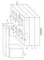


Classifications
-
- H—ELECTRICITY
- H05—ELECTRIC TECHNIQUES NOT OTHERWISE PROVIDED FOR
- H05K—PRINTED CIRCUITS; CASINGS OR CONSTRUCTIONAL DETAILS OF ELECTRIC APPARATUS; MANUFACTURE OF ASSEMBLAGES OF ELECTRICAL COMPONENTS
- H05K1/00—Printed circuits
- H05K1/02—Details
- H05K1/0201—Thermal arrangements, e.g. for cooling, heating or preventing overheating
- H05K1/0203—Cooling of mounted components
- H05K1/0204—Cooling of mounted components using means for thermal conduction connection in the thickness direction of the substrate
-
- H—ELECTRICITY
- H05—ELECTRIC TECHNIQUES NOT OTHERWISE PROVIDED FOR
- H05K—PRINTED CIRCUITS; CASINGS OR CONSTRUCTIONAL DETAILS OF ELECTRIC APPARATUS; MANUFACTURE OF ASSEMBLAGES OF ELECTRICAL COMPONENTS
- H05K7/00—Constructional details common to different types of electric apparatus
- H05K7/20—Modifications to facilitate cooling, ventilating, or heating
- H05K7/2039—Modifications to facilitate cooling, ventilating, or heating characterised by the heat transfer by conduction from the heat generating element to a dissipating body
- H05K7/20509—Multiple-component heat spreaders; Multi-component heat-conducting support plates; Multi-component non-closed heat-conducting structures
-
- H—ELECTRICITY
- H05—ELECTRIC TECHNIQUES NOT OTHERWISE PROVIDED FOR
- H05K—PRINTED CIRCUITS; CASINGS OR CONSTRUCTIONAL DETAILS OF ELECTRIC APPARATUS; MANUFACTURE OF ASSEMBLAGES OF ELECTRICAL COMPONENTS
- H05K7/00—Constructional details common to different types of electric apparatus
- H05K7/20—Modifications to facilitate cooling, ventilating, or heating
- H05K7/20218—Modifications to facilitate cooling, ventilating, or heating using a liquid coolant without phase change in electronic enclosures
- H05K7/20254—Cold plates transferring heat from heat source to coolant
-
- H—ELECTRICITY
- H01—ELECTRIC ELEMENTS
- H01R—ELECTRICALLY-CONDUCTIVE CONNECTIONS; STRUCTURAL ASSOCIATIONS OF A PLURALITY OF MUTUALLY-INSULATED ELECTRICAL CONNECTING ELEMENTS; COUPLING DEVICES; CURRENT COLLECTORS
- H01R12/00—Structural associations of a plurality of mutually-insulated electrical connecting elements, specially adapted for printed circuits, e.g. printed circuit boards [PCB], flat or ribbon cables, or like generally planar structures, e.g. terminal strips, terminal blocks; Coupling devices specially adapted for printed circuits, flat or ribbon cables, or like generally planar structures; Terminals specially adapted for contact with, or insertion into, printed circuits, flat or ribbon cables, or like generally planar structures
- H01R12/70—Coupling devices
- H01R12/71—Coupling devices for rigid printing circuits or like structures
- H01R12/712—Coupling devices for rigid printing circuits or like structures co-operating with the surface of the printed circuit or with a coupling device exclusively provided on the surface of the printed circuit
- H01R12/716—Coupling device provided on the PCB
-
- H—ELECTRICITY
- H05—ELECTRIC TECHNIQUES NOT OTHERWISE PROVIDED FOR
- H05K—PRINTED CIRCUITS; CASINGS OR CONSTRUCTIONAL DETAILS OF ELECTRIC APPARATUS; MANUFACTURE OF ASSEMBLAGES OF ELECTRICAL COMPONENTS
- H05K1/00—Printed circuits
- H05K1/02—Details
- H05K1/0201—Thermal arrangements, e.g. for cooling, heating or preventing overheating
- H05K1/0203—Cooling of mounted components
- H05K1/0204—Cooling of mounted components using means for thermal conduction connection in the thickness direction of the substrate
- H05K1/0206—Cooling of mounted components using means for thermal conduction connection in the thickness direction of the substrate by printed thermal vias
-
- H—ELECTRICITY
- H10—SEMICONDUCTOR DEVICES; ELECTRIC SOLID-STATE DEVICES NOT OTHERWISE PROVIDED FOR
- H10W—GENERIC PACKAGES, INTERCONNECTIONS, CONNECTORS OR OTHER CONSTRUCTIONAL DETAILS OF DEVICES COVERED BY CLASS H10
- H10W40/00—Arrangements for thermal protection or thermal control
- H10W40/20—Arrangements for cooling
- H10W40/22—Arrangements for cooling characterised by their shape, e.g. having conical or cylindrical projections
-
- H—ELECTRICITY
- H10—SEMICONDUCTOR DEVICES; ELECTRIC SOLID-STATE DEVICES NOT OTHERWISE PROVIDED FOR
- H10W—GENERIC PACKAGES, INTERCONNECTIONS, CONNECTORS OR OTHER CONSTRUCTIONAL DETAILS OF DEVICES COVERED BY CLASS H10
- H10W40/00—Arrangements for thermal protection or thermal control
- H10W40/40—Arrangements for thermal protection or thermal control involving heat exchange by flowing fluids
-
- H—ELECTRICITY
- H05—ELECTRIC TECHNIQUES NOT OTHERWISE PROVIDED FOR
- H05K—PRINTED CIRCUITS; CASINGS OR CONSTRUCTIONAL DETAILS OF ELECTRIC APPARATUS; MANUFACTURE OF ASSEMBLAGES OF ELECTRICAL COMPONENTS
- H05K2201/00—Indexing scheme relating to printed circuits covered by H05K1/00
- H05K2201/10—Details of components or other objects attached to or integrated in a printed circuit board
- H05K2201/10227—Other objects, e.g. metallic pieces
- H05K2201/10378—Interposers
-
- H—ELECTRICITY
- H05—ELECTRIC TECHNIQUES NOT OTHERWISE PROVIDED FOR
- H05K—PRINTED CIRCUITS; CASINGS OR CONSTRUCTIONAL DETAILS OF ELECTRIC APPARATUS; MANUFACTURE OF ASSEMBLAGES OF ELECTRICAL COMPONENTS
- H05K2201/00—Indexing scheme relating to printed circuits covered by H05K1/00
- H05K2201/10—Details of components or other objects attached to or integrated in a printed circuit board
- H05K2201/10227—Other objects, e.g. metallic pieces
- H05K2201/10416—Metallic blocks or heatsinks completely inserted in a PCB
Landscapes
- Engineering & Computer Science (AREA)
- Microelectronics & Electronic Packaging (AREA)
- Physics & Mathematics (AREA)
- Thermal Sciences (AREA)
- Structure Of Printed Boards (AREA)
- Cooling Or The Like Of Semiconductors Or Solid State Devices (AREA)
- Cooling Or The Like Of Electrical Apparatus (AREA)
- Secondary Cells (AREA)
- Non-Silver Salt Photosensitive Materials And Non-Silver Salt Photography (AREA)
- Hybrid Cells (AREA)
Description
本開示は、概して、配電に関し、より具体的には、冷却を伴うポイントオブロード(POL)からの配電に関する。 This disclosure relates generally to power distribution, and more specifically to power distribution from point-of-load (POL) with cooling.
ASIC(特定用途向け集積回路)プロセスノードが進歩し、デバイスの電力が増加し続けるにつれて、必要な電力を送達することがより困難になっている。より高い電力の分配はまた、追加の熱的課題を提示する。 As ASIC (application-specific integrated circuit) process nodes advance and device power continues to increase, it becomes more difficult to deliver the required power. The distribution of higher power also presents additional thermal challenges.
対応する参照文字は、図面のいくつかの図にわたって対応する部分を示す。 Corresponding reference characters indicate corresponding parts throughout the several views of the drawings.
概要
本発明の態様は、独立請求項で述べられ、好ましい特徴は、従属請求項で述べられる。一態様の特徴は、単独で、または他の態様と組み合わせて、任意の態様に適用され得る。
SUMMARY Aspects of the invention are set out in the independent claims and preferred features are set out in the dependent claims. Features from one aspect may be applied to any aspect alone or in combination with other aspects.
1つの実施形態では、装置は、概して、第1の表面および第1の表面とは反対側の第2の表面を備える基板と、基板の第1の表面に取り付けられた集積回路と、基板の第2の表面に取り付けられたコールドプレートであって、コールドプレートに接続された電源構成要素から集積回路に電力を伝送するために、電気経路がコールドプレートを貫いて延在する、コールドプレートと、を備える。 In one embodiment, the apparatus generally comprises a substrate having a first surface and a second surface opposite the first surface, an integrated circuit mounted on the first surface of the substrate, and a cold plate mounted on the second surface of the substrate, the cold plate having an electrical path extending therethrough for transmitting power from a power component connected to the cold plate to the integrated circuit.
1つ以上の実施形態において、コールドプレートは、電源構成要素から集積回路に電力を伝送するための複数の電気経路を備える。 In one or more embodiments, the cold plate includes multiple electrical paths for transmitting power from the power supply components to the integrated circuit.
1つ以上の実施形態において、電源構成要素は、電気接続を介して固定ポイントオブロード(POL)モジュールと相互接続された調整POLモジュールを備える。 In one or more embodiments, the power supply component includes a regulated point-of-load (POL) module interconnected with a fixed POL module via an electrical connection.
1つ以上の実施形態において、基板および集積回路は、マルチチップモジュールを備える。 In one or more embodiments, the substrate and integrated circuit comprise a multi-chip module.
1つ以上の実施形態において、集積回路は、ネットワーク処理機能を実行するように動作可能なASIC(特定用途向け集積回路)を備える。 In one or more embodiments, the integrated circuit comprises an ASIC (application specific integrated circuit) operable to perform network processing functions.
1つ以上の実施形態において、装置は、第2のコールドプレートと、第2のコールドプレートと集積回路との間に配置された熱インターポーザと、をさらに備える。 In one or more embodiments, the apparatus further includes a second cold plate and a thermal interposer disposed between the second cold plate and the integrated circuit.
1つ以上の実施形態において、コールドプレートは、コールドプレートに挿入された電力送達ブロックを備え、電気経路は、電力送達ブロックを貫いて延在する。 In one or more embodiments, the cold plate includes a power delivery block inserted into the cold plate, and the electrical path extends through the power delivery block.
1つ以上の実施形態において、電力送達ブロックは、プリント回路基板を備え、電気経路は、プリント回路基板内に形成された電力ビアを備える。 In one or more embodiments, the power delivery block comprises a printed circuit board and the electrical path comprises power vias formed within the printed circuit board.
1つ以上の実施形態において、電力は、少なくとも10アンペアの電流で、電力ビアを通して伝送される。 In one or more embodiments, power is transmitted through the power vias at a current of at least 10 amps.
1つ以上の実施形態において、コールドプレートは、コールドプレートに挿入された複数のプリント回路基板を備え、プリント回路基板の各々は、電気経路を形成する少なくとも1つの電力ビアを備える。 In one or more embodiments, the cold plate includes a plurality of printed circuit boards inserted into the cold plate, each of the printed circuit boards including at least one power via that forms an electrical path.
1つ以上の実施形態において、電源構成要素は、パルス電力を受け取るように構成されている。 In one or more embodiments, the power supply component is configured to receive pulsed power.
1つ以上の実施形態において、基板上の少なくとも1つの構成要素は、ファイバおよび銅の接続に結合されている。 In one or more embodiments, at least one component on the substrate is bonded to a fiber and copper connection.
1つ以上の実施形態において、コールドプレートは、コールドプレートを通して通信を伝送するための通信経路をさらに備える。 In one or more embodiments, the cold plate further comprises a communication path for transmitting communications through the cold plate.
1つ以上の実施形態において、コールドプレートは、コールドプレートを通して光学系を伝送するための開口部をさらに備える。 In one or more embodiments, the cold plate further comprises an opening for transmitting an optical system through the cold plate.
1つ以上の実施形態において、コールドプレートは、多相コールドプレートを含む。 In one or more embodiments, the cold plate comprises a multi-phase cold plate.
1つ以上の実施形態において、電源構成要素は、固定ポイントオブロード(POL)モジュールを備え、電気経路は、固定POLモジュールから集積回路に電力を送達するための、コールドプレート内に位置し、固定POLモジュールに結合された調整POLモジュールを備える。 In one or more embodiments, the power supply component includes a fixed point-of-load (POL) module, and the electrical path includes a regulated POL module located in the cold plate and coupled to the fixed POL module for delivering power from the fixed POL module to the integrated circuit.
別の実施形態では、装置は、概して、基板およびダイパッケージと電気的に結合された調整ポイントオブロード(POL)と相互接続された固定POLを備えるPOL電源と、調整POLと基板およびダイパッケージとの間に介装されたコールドプレートと、を備える。電力は、調整POLから基板およびダイパッケージに、コールドプレートを通して伝送される。 In another embodiment, an apparatus generally includes a POL power supply comprising a fixed point of load (POL) interconnected with a regulated POL electrically coupled to the substrate and die package, and a cold plate interposed between the regulated POL and the substrate and die package. Power is transferred from the regulated POL to the substrate and die package through the cold plate.
別の実施形態では、装置は、概して、ポイントオブロード(POL)モジュールを受容するように構成された上面と、少なくとも1つのダイが取り付けられた基板に取り付けるように構成された下面とを備えるコールドプレートと、POLモジュールから、基板に取り付けられたダイに、電力を送達するための、コールドプレートに挿入され、少なくとも1つの電力ビアを備える電力送達ブロックと、を備える。 In another embodiment, an apparatus generally includes a cold plate having an upper surface configured to receive a point-of-load (POL) module and a lower surface configured to be attached to a substrate having at least one die attached thereto, and a power delivery block inserted into the cold plate and including at least one power via for delivering power from the POL module to the die attached to the substrate.
さらに別の実施形態では、方法は、概して、電力送達ブロックをコールドプレートに挿入することであって、電力送達ブロックは、コールドプレートの第1の表面からコールドプレートの第2の表面まで延在する電気経路を備える、挿入することと、ポイントオブロード(POL)モジュールをコールドプレートの第1の表面に取り付けることと、基板をコールドプレートの第2の表面に取り付けることであって、ダイが、基板の反対側に取り付けられている、取り付けることと、を含む。電力は、POLモジュールからダイに、コールドプレート内の電力送達ブロックを通して分配される。 In yet another embodiment, a method generally includes inserting a power delivery block into a cold plate, the power delivery block comprising an electrical path extending from a first surface of the cold plate to a second surface of the cold plate, attaching a point-of-load (POL) module to the first surface of the cold plate, and attaching a substrate to the second surface of the cold plate, the die being attached to an opposite side of the substrate. Power is distributed from the POL module to the die through the power delivery block in the cold plate.
本明細書に記載の実施形態の特徴および利点のさらなる理解は、本明細書の残りの部分および添付の図面を参照することによって実現することができる。 A further understanding of the features and advantages of the embodiments described herein can be realized by reference to the remaining portions of the specification and the attached drawings.
例示的な実施形態
以下の説明は、当業者が実施形態を作成および使用することを可能にするために提示される。特定の実施形態および用途の説明は、例としてのみ提供されており、様々な変更形態が当業者には容易に明らかになるであろう。本明細書に記載の一般原理は、実施形態の範囲から逸脱することなく、他の用途に適用することができる。したがって、実施形態は、示されているものに限定されるべきではなく、本明細書に記載されている原理および特徴と一致する最も広い範囲を与えられるべきである。明確にするために、実施形態に関連する技術分野で知られている技術資料に関連する詳細は、詳細には説明されていない。
Exemplary embodiments The following description is presented to enable those skilled in the art to make and use the embodiments. Descriptions of specific embodiments and applications are provided only as examples, and various modifications will be readily apparent to those skilled in the art. The general principles described herein can be applied to other applications without departing from the scope of the embodiments. Thus, the embodiments should not be limited to those shown, but should be accorded the widest scope consistent with the principles and features described herein. For clarity, details related to technical materials known in the technical field related to the embodiments have not been described in detail.
配電システムは、ポイントオブロード(POL)からASIC(特定用途向け集積回路)または他の集積回路に電力を送達するように構成され得る。電力要件が増加すると、追加の熱的考慮が必要になる場合がある。パッケージ内の光学アプリケーションは、追加の課題を提示する場合がある。例えば、ファイバおよび銅のアタッチメント(FAU(ファイバアタッチメント(アレイ)ユニット)、CAU(銅アタッチメント(アレイ)ユニット))は、冷却液に影響を与えるクリアランス要件を導入する場合がある。 Power distribution systems may be configured to deliver power from a point-of-load (POL) to an ASIC (Application Specific Integrated Circuit) or other integrated circuits. Increased power requirements may require additional thermal considerations. Optical applications within a package may present additional challenges. For example, fiber and copper attachments (FAU (Fiber Attachment (Array) Unit), CAU (Copper Attachment (Array) Unit)) may introduce clearance requirements that impact cooling fluids.
本明細書に記載の実施形態は、基板がコールドプレートの片側に隣接して配置され、POL構成要素がコールドプレートの反対側に置かれた、電力送達および冷却構成を提供する。以下で詳細に説明するように、電気経路が、コールドプレート内に形成され、電力がPOLから、基板に結合された電子部品(ダイ、集積回路、ASIC、チップ)に渡されることを可能にする。コールドプレートは、例えば、コールドプレートを通して電力を移送するための1つ以上の電力ビアを有する電力送達ブロック(例えば、PCB(プリント回路基板))を備え得る。別の実施例では、コールドプレートは、コールドプレートを通して電力を移送するための電源構成要素(例えば、調整POL)を備え得る。 The embodiments described herein provide a power delivery and cooling configuration in which a substrate is positioned adjacent to one side of a cold plate and POL components are placed on the opposite side of the cold plate. As described in more detail below, electrical paths are formed in the cold plate to allow power to be passed from the POL to electronic components (die, integrated circuit, ASIC, chip) coupled to the substrate. The cold plate may, for example, comprise a power delivery block (e.g., PCB (printed circuit board)) having one or more power vias for transferring power through the cold plate. In another example, the cold plate may comprise a power supply component (e.g., regulated POL) for transferring power through the cold plate.
1つ以上の実施形態において、装置は、基板およびダイパッケージと電気的に結合された調整POLと相互接続された固定POLを備えるPOL電源と、調整POLと基板およびダイパッケージとの間に介装されたコールドプレートと、を備える。電力は、調整POLから基板およびダイパッケージにコールドプレートを通して伝送される。追加の冷却が必要な場合は、基板およびダイパッケージを2つのコールドプレート間に配置し得る。1つ以上の実施形態において、大量の電流(例えば、≧500アンペア、≧1000アンペア)が基板およびダイパッケージ内に移送され、それによって、改善された効率が可能になる。 In one or more embodiments, the apparatus includes a POL power supply comprising a fixed POL interconnected with a regulating POL electrically coupled to the substrate and die package, and a cold plate interposed between the regulating POL and the substrate and die package. Power is transferred from the regulating POL to the substrate and die package through the cold plate. If additional cooling is required, the substrate and die package may be placed between two cold plates. In one or more embodiments, a large amount of current (e.g., ≧500 amps, ≧1000 amps) is transferred into the substrate and die package, thereby enabling improved efficiency.
本明細書に記載の実施形態は、複数のネットワークデバイスを含むデータ通信ネットワークの文脈で動作する。ネットワークは、ネットワーク内のデータの通過を容易にする任意の数のノード(例えば、ルータ、スイッチ、ゲートウェイ、コントローラ、エッジデバイス、アクセスデバイス、集約デバイス、コアノード、中間ノード、電源器、動力デバイス、または他のネットワークデバイス)を介して通信する、任意の数のネットワークデバイスを含み得る。ネットワークデバイスのうちの1つ以上は、本明細書に記載の1つ以上の配電システムを備え得る。ネットワークデバイスは、メモリ、プロセッサ、電源ユニット、およびネットワークインターフェースの任意の組み合わせをさらに含み得る。 The embodiments described herein operate in the context of a data communications network including multiple network devices. The network may include any number of network devices communicating through any number of nodes (e.g., routers, switches, gateways, controllers, edge devices, access devices, aggregation devices, core nodes, intermediate nodes, power supplies, power devices, or other network devices) that facilitate the passage of data through the network. One or more of the network devices may comprise one or more power distribution systems described herein. The network devices may further include any combination of memory, processors, power units, and network interfaces.
ここで図面を、まず図1を、参照すると、1つの実施形態による、ボード10上に位置するPOL電源を通しての配電の一実施例を示すブロック図が示されている。電力は、要素12で、複数のPOL(POLモジュール(回路)、電源構成要素)14a、14c、14d、14eに送達される。1つの実施例では、100Vよりも大きい電圧(例えば、108V、380V)または任意の他の好適な電圧のパルス電力が、固定POL14aに送達される。電源12はまた、パルス電力をPOL14c、14d、および14e(例えば、固定POL)にも送達し得る。別の実施例では、電源12は、54VDC(または任意の他の好適な電圧(例えば、システム全体の効率、ルーティング可能性、およびコストに基づいて選択された中間バス電圧レベル))をPOLモジュール14c、14d、14eに送達する。固定POL14aは、電力(例えば、54VDCまたは他の電圧)を、調整POL(POLコンバータ、POLレギュレータ)14bに移送し、調整POL14bは、ASIC16(例えば、集積回路、ダイ、チップ、マルチチップモジュールなど)に電力を分配する。以下に説明するように、固定POL14aは、調整POL14bに、バスバー相互接続または任意の他の好適な電気接続を通して接続され得る。調整POL14bは、例えば、150アンペア以上の出力を提供し得る。各電源接続は、例えば、10Mbps(または任意の他のデータ速度)の通信を含み得る。図1に示された実施例では、電力は、調整POLモジュール14bからASIC16に電圧レールを介して送達される。電力は、例えば、マルチドロップ構成でASIC16に提供され得る。 Now referring to the drawings, and first to FIG. 1, a block diagram is shown illustrating one example of power distribution through a POL power supply located on board 10, according to one embodiment. Power is delivered at element 12 to multiple POLs (POL modules (circuits), power supply components) 14a, 14c, 14d, 14e. In one example, pulsed power of a voltage greater than 100V (e.g., 108V, 380V) or any other suitable voltage is delivered to fixed POL 14a. Power supply 12 may also deliver pulsed power to POLs 14c, 14d, and 14e (e.g., fixed POLs). In another example, power supply 12 delivers 54VDC (or any other suitable voltage (e.g., intermediate bus voltage level selected based on overall system efficiency, routability, and cost)) to POL modules 14c, 14d, 14e. The fixed POL 14a transfers power (e.g., 54 VDC or other voltage) to the regulated POL (POL converter, POL regulator) 14b, which distributes the power to the ASIC 16 (e.g., an integrated circuit, die, chip, multi-chip module, etc.). As described below, the fixed POL 14a may be connected to the regulated POL 14b through a bus bar interconnect or any other suitable electrical connection. The regulated POL 14b may provide, for example, 150 amps or more of output. Each power connection may include, for example, 10 Mbps (or any other data rate) communication. In the example shown in FIG. 1, power is delivered from the regulated POL module 14b to the ASIC 16 via a voltage rail. Power may be provided to the ASIC 16 in a multi-drop configuration, for example.
本明細書で使用される場合、「POLモジュール」という用語は、例えば、個別のPOLおよびモジュール、または電力送達ブロックベースの電圧調整器の設計を含む、様々なタイプのPOL構成を指し得ることを理解されたい。また、POLは、1つ以上の出力を送達するために一緒に働き得る単相または多相のPOLであり得ることが分かり得る。 As used herein, it should be understood that the term "POL module" may refer to various types of POL configurations, including, for example, individual POLs and modules, or power delivery block-based voltage regulator designs. It should also be understood that the POLs may be single-phase or multi-phase POLs that may work together to deliver one or more outputs.
システム構成要素(POLモジュール、コールドプレート、電子パッケージ(基板およびダイパッケージ))は、ボード10に接続されている。ボード10は、プリント回路基板を備えてもよいし、または構成要素は、板金モジュール、配線カード、もしくは任意の他の好適な支持部材に直接取り付けられてもよい。例えば、配線カード回路基板を取り外して、ASIC縁部でファイバおよび銅の接続を通して電子パッケージを相互接続してもよい。 The system components (POL module, cold plate, electronics package (substrate and die package)) are connected to the board 10. The board 10 may comprise a printed circuit board, or the components may be mounted directly to a sheet metal module, wiring card, or any other suitable support member. For example, the wiring card circuit board may be removed and the electronics package interconnected through fiber and copper connections at the ASIC edge.
前述のように、POLモジュールのうちの1つ以上に、パルス電力が供給され得る。本明細書で使用される場合、(「パルス化電力」とも称される)「パルス電力」という用語は、電圧が、パルスオフ時間19a中の(例えば、0V、3Vに近い)非常に小さい電圧と、パルスオン時間19b中のより大きな電圧(例えば、≧12V)との間で変化する、複数の電圧パルス(一連の電圧パルス)18で送達される電力を指す。動力デバイスに電力供給する際に使用するために、高電圧パルス電力(高電圧パルス)(例えば、>56V、≧60V、≧300V)が、電源器(PSE)から動力デバイス(PD)に伝送され得、一方、起動(例えば、初期化、同期化、ローカルエネルギー貯蔵器の充電、コントローラの電源投入、試験、またはそれらの任意の組み合わせ)のために、低電圧パルス電力(低電圧パルス)(例えば、約12V、約24V、≦30V、≦56V)が、短い間隔で使用され得る。パルス電力はまた、連続電力を提供するために、相間でパルスが互いにオフセットされて、複数の相で送達され得る。パルス送電は、例えば、ケーブル、伝送ライン、バスバー、バックプレーン、PCB、および配電システムを通して行われ得る。 As mentioned above, one or more of the POL modules may be supplied with pulsed power. As used herein, the term "pulsed power" (also referred to as "pulsed power") refers to power delivered in multiple voltage pulses (series of voltage pulses) 18, where the voltage varies between a very small voltage (e.g., close to 0V, 3V) during the pulse off time 19a and a larger voltage (e.g., ≧12V) during the pulse on time 19b. High voltage pulsed power (high voltage pulse) (e.g., >56V, ≧60V, ≧300V) may be transmitted from the power supply (PSE) to the powered device (PD) for use in powering the powered device, while low voltage pulsed power (low voltage pulse) (e.g., about 12V, about 24V, ≦30V, ≦56V) may be used for short intervals for start-up (e.g., initialization, synchronization, charging a local energy store, powering up the controller, testing, or any combination thereof). Pulsed power can also be delivered on multiple phases, with the pulses offset from one another between phases to provide continuous power. Pulsed power can be delivered, for example, through cables, transmission lines, bus bars, backplanes, PCBs, and power distribution systems.
本明細書に記載の電圧、電力、および電流のレベルは、例としてのみ提供されており、電力は、実施形態の範囲から逸脱することなく、本明細書に記載されるものとは異なるレベル(ボルト、アンペア、ワット)で送達され得ることを理解されたい。また、電力は、ESP(拡張安全電力)(例えば、パルス電力、多相パルス電力、障害検出および安全保護を備えたパルス電力)、PoE(Power over Ethernet)として、または現在の標準もしくは将来の標準に従って、送達され得る。 It should be understood that the voltage, power, and current levels described herein are provided by way of example only, and that power may be delivered at different levels (volts, amps, watts) than those described herein without departing from the scope of the embodiments. Power may also be delivered as ESP (Extended Safety Power) (e.g., pulsed power, multi-phase pulsed power, pulsed power with fault detection and safety protection), PoE (Power over Ethernet), or in accordance with current or future standards.
図2は、1つの実施形態による、固定POL20と調整POL22との間の接続と、コールドプレート25を通しての電力の分配と、を示す概略斜視図である。固定POLモジュール20は、入力電力を調整POLモジュール22に、例えば、バスバー、ワイヤ、または他の相互接続を含む電気接続24を介して提供し得る。簡略化のために、1つのPOLモジュール22のみがコールドプレート25に接続されて示されているが、任意の数のPOLモジュールがコールドプレートに接続され得る。各POLは、図1に示されたように、単一の電圧レールまたは複数の電圧レールを提供し得る。
2 is a schematic perspective view showing the connections between the fixed
図2に示されるように、コールドプレート25は、コールドプレートを通して、POLモジュール22から(図4に関して以下で説明する)電子パッケージ(基板およびダイパッケージ)に電力を伝送するための複数の電力ビア(電気経路)28を各々が備える複数の電力送達ブロック26を備える。電力は、コールドプレート25の第1の側(例えば、図2に示されるように上面27a)から、第1の側とは反対側でほぼ平行な第2の側(例えば、図2に示されるように下面27b)に伝送される。1つ以上の実施形態において、電力送達ブロック26は、小さな(ミニチュアの)電力プリント回路基板を備える。用途に基づいて、他の構成要素もまたコールドプレート25に挿入されてもよいし、または戦略的に置かれた切り抜き部が使用されてもよい。
2, the
本明細書で使用され得る、下方の、上方の、底部の、頂部の、下方に、上方に、水平な、垂直ななどの用語は、パッケージおよび構成要素の配向に依存する相対的な用語であり、制限的に解釈されるべきではないことに留意されたい。これらの用語は、参照ポイントを説明するものであり、実施形態を任意の特定の配向または構成に限定するものではない。 Note that terms such as lower, upper, bottom, top, lower, upper, horizontal, vertical, etc. that may be used herein are relative terms that depend on the orientation of the package and components and should not be construed as limiting. These terms are intended to describe points of reference and do not limit the embodiments to any particular orientation or configuration.
電力送達ブロック26は、(図3に仮想線で示されているように)電力送達ブロックの全厚を貫いて延在し、それらの内部表面に沿ってめっきされている複数の貫通孔(ビア)28を備える。貫通孔は、例えば、ドリル穿孔プロセスを使用して作成され、金属材料(例えば、銅または任意の導電性もしくは金属の層)でめっきされ得る。めっきは、効果的に、孔の円筒を覆い、コールドプレート25を貫く電気経路を作成し得る。
The
本明細書で使用される場合、「電力送達ブロック」という用語は、コールドプレート25を直接通る電力の通過を可能にするように、電気経路(例えば、電力ビア)が形成され得る、熱的かつ導電性の材料の任意のブロックを指し得る。「プリント回路基板」という用語は、本明細書では、電力送達ブロック26のための基板の一実施例として使用されるが、他の実装形態では、PCBは、他の基板(例えば、セラミック回路基板)または他の要素で置き換えられ得る。また、電力送達ブロック26には、非プリント回路基板が使用されてもよい。例えば、ガラス片を、導波路を付けてレーザーパターン化し、金属ビアを付けてめっきして、光学経路と電気経路の組み合わせを形成してもよい。また、前述のように、PCBに加えて、またはPCBの代わりに、他の構成要素をコールドプレートに挿入してもよい。
As used herein, the term "power delivery block" may refer to any block of thermally and electrically conductive material in which electrical paths (e.g., power vias) may be formed to allow the passage of power directly through the
コールドプレート25は、例えば、液体、気体、または多相(多相コールドプレート)ベースの冷却を備え得る。貫通電力ビア28は、例えば、管あたり10アンペアを送達し得、コールドプレート25によって冷却され得る。1つ以上の実施形態において、コールドプレート25は、1つ以上の電力送達ブロック26を挿入するための1つ以上の開口部を備えて形成され、電力送達ブロック26は、例えば、コールドプレート25に圧入され得る。エポキシ樹脂または接着剤の充填物を使用して、電力送達ブロック26をコールドプレート25内に押し込んで配置し得る。エポキシ樹脂は、電力送達ブロック26とコールドプレート開口部との間の許容誤差を占めるように使用され得る。コールドプレート25が冷却管またはリザーバを利用する場合、これらは、電力送達ブロック開口部の周りに経路設定または配置される。コールドプレート25は、電力ビア28の温度上昇を低く保ち、それにより、POL22から基板およびダイパッケージへの電流移送を最大化する。1つの実施例では、コールドプレート25は、光学温度を摂氏75度未満に維持するための複数の内部ゾーンを有して構成される。コールドプレートにわたる温度分布の一例を図11に示し、以下に説明する。本明細書に記載のコールドプレートおよび温度は、単なる例であり、他の設計を使用して、異なる温度で冷却を維持し得ることを理解されたい。
The
図3に示されるように、電力送達ブロック26およびそこに形成されたビア28は、コールドプレート25を貫いて延在し、取り付けられた電子パッケージ(基板およびダイパッケージ)31に電力を提供する。簡略化のために、電力送達ブロック26およびビア28の一部分のみが、コールドプレート25を貫いて延在する仮想線で示されている。また、電子パッケージ31は、単一のブロック構造として示されているが、パッケージは、図4に関して以下で説明するように、任意の数の構成要素(集積回路、ASIC、ダイ、チップ、チップレット、光学エンジン、FAU/CAU)がそれに取り付けられた、1つ以上の基板を備え得ることを理解されたい。
As shown in FIG. 3, the
1つ以上の実施形態において、装置は、ポイントオブロード(POL)モジュール22を受容するように構成された上面27aと、(図4に示され、以下に説明されるように)少なくとも1つのダイが取り付けられた基板に取り付けられるように構成された下面27bとを有するコールドプレート25を備え、電力送達ブロック26が、コールドプレートに挿入され、POLモジュールから、基板に取り付けられたダイに、電力を送達するための電力ビア28を備える。
In one or more embodiments, the apparatus includes a
1つ以上の実施形態において、追加のコールドプレート37を使用して、電子パッケージ31が2つのコールドプレート25、37の間に介装されて、電子パッケージに追加の冷却を提供し得る。第2の冷却プレート37の使用は、電力および冷却要件に基づいて任意選択的であることが分かり得る。図5、図6、図7、および図8の実施例には、第2の冷却プレートは示されていないが、第2の冷却プレートを使用してもよい。
In one or more embodiments, an additional
また、コールドプレートは、任意の数の個別のコールドプレートを含み得ることを理解されたい。例えば、コールドプレート25は、2つ以上のより小さなコールドプレートを含み、電力送達ブロックまたは電気経路のうちの1つ以上がそれらの間に介装され得る。
It should also be understood that the cold plate may include any number of individual cold plates. For example,
ここで図4を参照すると、断面概略図は、第1の表面41aおよび第1の表面とは反対側の第2の表面41bを有する基板41と、基板の第1の表面に取り付けられた集積回路(1つ以上のダイ(チップ))43と、基板の第2の表面に取り付けられ、電源構成要素(例えば、POLモジュール)42から集積体に電力を伝送するためにそれを貫いて延在する電気経路(例えば、電力ビア)48を備えるコールドプレート45と、を備える装置を示す。本明細書で使用される場合、「基板」という用語は、電気基板、セラミック基板、または任意の他の好適な材料から形成される要素を指し得る。
4, a cross-sectional schematic diagram shows an apparatus comprising a
POLモジュールから、基板41と、それに取り付けられた集積回路43(ASIC、NPU(ネットワーク処理ユニット)、ダイ、チップ)および2つの光学エンジン(フォトニックチップ)49(SerDes(シリアライザ/デシリアライザ)チップレット)とを備える電子パッケージに、電力を分配するように構成されたコールドプレート45に取り付けられたPOLモジュール42を有する(例えば、レール電圧へのDC電力を有する)マルチゾーンPOL40に、バスバー44が接続されて示されている。(本明細書では基板およびダイパッケージとも称される)電子パッケージは、1つ以上の基板に取り付けられた1つ以上の集積回路、ASIC、NPU、MCM、ダイ、チップ、チップレット、プロセッサ、または電子部品を備え得る。図4の実施例では、基板およびダイパッケージは、基板41、NPU43、光学エンジン49、およびFAU/CAU50を含む。これは、単なる一実施例であり、基板およびダイパッケージは、任意の数の構成要素を任意の構成で含み得ることを理解されたい。FAU/CAU50は、(図4に示されたように)光学エンジン49の下面に取り付けられてもよいし、または光学エンジン49の上面または側面に配置されてもよい。図4の実施例では、第2のコールドプレート47が、熱導体(インターポーザ)51を通してNPU43に熱的結合されている。熱導体(または複数の熱導体)は、複数のダイにまたがって配置され得る。1つ以上の実施形態はまた、マルチチップモジュールとコールドプレート47との間に任意選択的な蓋を含み得る。
A bus bar 44 is shown connected to a multi-zone POL 40 (e.g., having DC power to rail voltages) having a POL module 42 mounted on a cold plate 45 configured to distribute power from the POL module to an electronic package comprising a
前述のように、コールドプレート45は、コールドプレートに挿入された1つ以上の電力送達ブロック46(例えば、PWR PCB)を含み、1つ以上の電気経路(電力ビア)48がその中に形成されている。1つ以上の実施形態において、電力送達ブロック46は、コールドプレート45とは別に形成され、ブロックを受容するためにコールドプレートに形成された開口部56に挿入される。上記したように、エポキシ樹脂または接着剤の充填物を使用して、コールドプレート45の開口部56内に電力送達ブロックを押し込んで配置し得る。 As previously mentioned, the cold plate 45 includes one or more power delivery blocks 46 (e.g., PWR PCBs) inserted into the cold plate and having one or more electrical paths (power vias) 48 formed therein. In one or more embodiments, the power delivery blocks 46 are formed separately from the cold plate 45 and inserted into openings 56 formed in the cold plate to receive the blocks. As noted above, an epoxy or adhesive filler may be used to press and place the power delivery blocks into the openings 56 in the cold plate 45.
基板41は、電力ビア48およびダイ43と接続するために、基板内に埋め込まれるかまたは基板上に堆積されたトレース53およびパッド55を備え得る。当業者にはよく知られているように、エッチング、堆積、ボンディング、または他のプロセスを使用して、トレースおよびパッドを形成し得る。基板41は、当業者にはよく知られているように、はんだプロセスを使用してコールドプレート45にボンディングし得る。
The
1つの実施例では、図4に示されるアセンブリ全体は、50mm未満の高さを有し得る。例えば、POLモジュール42は、約15mm~20mmの高さを有し得、コールドプレート45、47は、各々、約5mm~8mmの高さを有し得、光学エンジン49は、約2mm~3mmの高さを有し得る。パッケージは、例えば、70mmx70mm以上であり得る。図4に示されるこれらの寸法ならびに構成要素および構成は、単なる実施例であり、異なるサイズおよび構成を有する他のタイプもしくは数の構成要素、または追加の構成要素を、実施形態の範囲から逸脱することなく、使用し得ることを理解されたい。例えば、1つ以上の集積回路を、コールドプレート45の上面(基板41とは反対の側)に配置してもよい。
In one example, the entire assembly shown in FIG. 4 may have a height of less than 50 mm. For example, the POL module 42 may have a height of about 15 mm to 20 mm, the cold plates 45, 47 may each have a height of about 5 mm to 8 mm, and the
図5は、図2に示されたコールドプレート25の下方の基板およびダイパッケージ(基板41、ASIC43、フォトニックチップ49、FAU/CAU50)の配置を概略的に示す。前述のように、基板41は、コールドプレート25の上面に配置された1つ以上のPOLモジュール22から電力を受け取るように動作可能な任意の数のASIC43を備えてもよいし、または個々の基板およびダイパッケージが、コールドプレートの方下に配置されてもよい。
Figure 5 shows a schematic of the arrangement of substrate and die packages (
電力に電力送達ブロック26を通過させることに加えて、通信(例えば、コントロールプレーン通信)もまた、電力送達ブロックを通過し得る。1つ以上の実施形態において、システムFPGA(フィールドプログラマブルゲートアレイ)への調整POLおよびASICのコントロール通信は、コールドプレート25またはリボンケーブルを通過し得る。
In addition to passing power through the
図6は、コントロールプレーン通信が、POL回路(POLモジュール60、62、および相互接続)と、電力ビア28とともに電力送達ブロック66内に形成された通信ビア68とを通過する一実施例を示す。図6に示された実施例では、コントロールプレーン通信は、経路64a通って固定POLを通過し、64bにおいて相互接続を通過し、64cにおいて調整POL62を通過する。電力送達ブロック66は、電力ビア28に加えて、通信ビア68を含んで、コールドプレート25を貫く、基板およびダイパッケージ31までの電気経路および通信経路を提供する。1つの実施例では、低速通信が、POLを通過する(例えば、200Mbpsの範囲)。コールドプレート25は、電力ビア、通信ビア、または電力ビアおよび通信ビアの両方を有する電力送達ブロックの任意の組み合わせを含み得る。
Figure 6 shows an example where control plane communications pass through the POL circuitry (
図7は、コントロールプレーン通信が、コントロール通信をパッケージに出し入れするために使用され得る別個の通信要素70、71を通して(例えば、リボンケーブルまたは他の手段を介して)提供される別の実施例を示す。通信モジュール71は、コールドプレート25に挿入された通信ブロック76(例えば、PCB)とインターフェースする。通信ブロック76は、その中に形成された1つ以上の通信経路(ビア)78を含む。1つ以上の実施形態において、全速PCIe(ペリフェラルコンポーネントインターコネクトエクスプレス)またはそれより高速なものを使用し得る。コールドプレート25は、任意の数または組み合わせのPOLモジュール22および通信モジュール(COMM71)に接続され得る。
Figure 7 shows another example where control plane communications are provided through separate communication elements 70, 71 (e.g., via ribbon cables or other means) that may be used to route control communications in and out of the package. The communication module 71 interfaces with a communication block 76 (e.g., PCB) inserted into the
1つ以上の実施形態において、光学系が、コールドプレートおよび基板を通過し得、したがって、電力接続および光学系接続の両方がPOLおよびバスバーに存在する。図8は、光がコールドプレート85およびパッケージ基板を通過して光学エンジン(フォトニックダイ)49に到達することを可能にするように通路が作成されている一実施例を示す。通路80は、例えば、光、ガラス中のレーザー書き込み導波路、自由空間光学系、または光ファイバに対して構成され得る。コールドプレート85および基板81に切り抜き部が作られて、POLモジュール82およびバスバー24をフォトニクスチップ49にリンクさせるために、通路80が、その中に挿入され得る。通路80は、例えば、光学アセンブリを画定する1つ以上の導波路または光ファイバを受容するための開口部を備え得る。通路構造80は、図8に示されたように、フォトニクスダイ49および電力ブリッジ(電源構成要素)に位置合わせして露出させてもよいし、または、例えば、インターロック機能を有するコネクタを通して相互接続してもよい。通路80は、例えば、屈折率整合エポキシなどの、能動的または受動的位置合わせプロセスおよび接着剤を使用して、ダイに取り付けられ得る。また、前述のように、光学経路は、電気経路と組み合わされ得る。例えば、ガラス片を、導波路を付けてレーザーパターン化し、金属ビアを付けてめっきして、光学経路と電気経路の組み合わせを形成し得る。また、1つ以上のフォトニックダイ49と通信するために、コールドプレート85および基板81に2つ以上の通路80を形成してもよい。
In one or more embodiments, the optics may pass through the cold plate and substrate, so that both the power and optics connections are present in the POL and busbar. FIG. 8 shows an example in which passages are created to allow light to pass through the
1つ以上の実施形態において、光学系のための通路構造80は、電子機器とは別個の光学経路のための専用切り抜き部の一部であり得る。例えば、図7の通信について上記に説明した実施形態と同様に、電力送達ブロック26のうちの1つ以上が、光学通路構造で置き換えられ得る。
In one or more embodiments, the
図9は、1つの実施形態による、電力送達ブロック96の概略斜視図である。前述のように、電力送達ブロック96は、複数の層90a、90b、90c、90dを備えるプリント回路基板または他の基板を備え得る。内側プレーン層90b、90cは、より大きな電流密度を提供し得る。プレーンを追加して、電力送達構造内にLC(インダクタ(L)、コンデンサ(C))フィルタリングを設けるための電力フィルタ形状を提供し得る。図9に示された実施例では、2つのPCBが使用され、それらの間に構成要素94が介装されている(例えば、コンデンサ、インダクタ、POL構成要素、FET(電界効果トランジスタ)コントローラなど)。電力送達ブロックは、任意の数の層、単一のブロック、構成要素がそれらの間に設置された複数のブロック、および電力または通信用の任意の数のビア92を含み得ることを理解されたい。 9 is a schematic perspective view of a power delivery block 96 according to one embodiment. As previously mentioned, the power delivery block 96 may comprise a printed circuit board or other substrate comprising multiple layers 90a, 90b, 90c, 90d. The inner plane layers 90b, 90c may provide greater current density. Planes may be added to provide power filter geometries to provide LC (inductor (L), capacitor (C)) filtering within the power delivery structure. In the example shown in FIG. 9, two PCBs are used with components 94 interposed between them (e.g., capacitors, inductors, POL components, FET (field effect transistor) controllers, etc.). It should be understood that the power delivery block may include any number of layers, a single block, multiple blocks with components placed between them, and any number of vias 92 for power or communication.
図10は、1つの実施形態による、配電および冷却システムを実装するためのプロセスの概要を示すフローチャートである。ステップ100で、電力送達ブロック46がコールドプレート45に挿入される(図4および図10)。前述のように、電力送達ブロックは、それを貫いて延在する1つ以上の電気経路(電力ビア)を有するPCBまたは他の基板を備え得る。電力送達ブロック46は、コールドプレート45に押し込まれ、例えば、エポキシ樹脂または接着剤の充填物で所定の位置に固定され得る。POLモジュール42が、コールドプレートの第1の表面(図4の上面)に取り付けられ(ステップ102)、ダイ43を有する基板41が、コールドプレートの第2の表面(図4の下面)に取り付けられる(ステップ104)。電力は、POLモジュールからダイに、コールドプレート内の電力送達ブロックを通して分配される(ステップ106)。
Figure 10 is a flow chart outlining a process for implementing a power distribution and cooling system, according to one embodiment. At step 100, a power delivery block 46 is inserted into the cold plate 45 (Figures 4 and 10). As previously mentioned, the power delivery block may comprise a PCB or other substrate having one or more electrical paths (power vias) extending therethrough. The power delivery block 46 may be pressed into the cold plate 45 and secured in place, for example, with a filler of epoxy or adhesive. A POL module 42 is attached to a first surface (top surface in Figure 4) of the cold plate (step 102), and a
図10に示され、上で説明されたプロセスは、単なる一実施例であり、実施形態の範囲から逸脱することなく、ステップを追加、改変、組み合わせ、または並べ替えることが可能であることを理解されたい。例えば、光学通路80が使用される場合、通路は、まずダイ/光学エンジンに取り付けられ得る。
It should be understood that the process shown in FIG. 10 and described above is merely an example, and steps may be added, modified, combined, or rearranged without departing from the scope of the embodiments. For example, if an
図11は、1つの実施形態による、コールドプレートにわたる温度分布の一例を示す側面図である。POLモジュール122は、前述のように、電力ビア128を備える第1のコールドプレート125に取り付けられている。基板およびダイパッケージ131が、第1のコールドプレート125の反対側に配置され、第1のコールドプレート125と第2のコールドプレート137との間に介装されている。前述のように、熱導体が、ダイと第2のコールドプレート137との間に配置され得る。コールドプレート125および137を通る流れの方向は、コールドプレート上の矢印で示されている。図11に示される温度分布の例は、1800Wパッケージで、入口温度が摂氏20度、流量が5.0LPM(2x2.5LPM)の場合である。
11 is a side view of an example of a temperature distribution across a cold plate, according to one embodiment. The POL module 122 is attached to a first
図12は、1つの実施形態による、コールドプレート125および電力送達ブロック126の平面図である。流れの方向は、矢印で示されているように、入口マニホルド127から排出マニホルド129である。電力ビア128を有する4つの電力送達ブロック126が、コールドプレート125に挿入されている。1つの実施例では、コールドプレート125は、所与の断面で均一な流れを得るために、可変のフィン密度を有する。例えば、コールドプレート125は、外縁に沿った低密度フィンカラム140と、コールドプレートの中央部分に沿った高密度フィンカラム142とを含み得る。1つの実施例では、第2のコールドプレート137(図11)は、均一なフィン密度を有し得る。フィンのピッチ、厚さ、フィンの数、およびマニホルドチャネル寸法は、圧力降下を最小限に抑え、両方のコールドプレートでほぼ均一な流れを得るように、最適化され得る。
12 is a plan view of the
図13は、配電システムの別の実施形態を示す。図13に示される実施例では、調整POLモジュール152が、コールドプレート155に形成された開口部に直接挿入されている。調整POLモジュール152は、前述したように、固定POLから、コールドプレート(図示せず)の反対側に取り付けられた基板およびダイパッケージに電力を送達するために、固定POLモジュール150に各々、接続され得る。この実施形態では、調整POLモジュール152は、接続154を通して調整POLモジュールに結合された固定POLモジュール150からの電気経路を画定している。埋め込みPOLモジュール152のために、熱インターフェースまたは熱伝達経路が設けられ得る。
13 illustrates another embodiment of a power distribution system. In the example shown in FIG. 13, the
前述から認められるように、本明細書に記載の1つ以上の実施形態は、従来のシステムに勝る利点を提供する。例えば、1つ以上の実施形態は、大量の電流を電子パッケージに高効率で移送すること(例えば、≧1000アンペア)を可能にする。1つ以上の実施形態において、コールドプレート(または複数のコールドプレート)、基板、およびダイの構成により、改善された熱効率が可能になる。コールドプレートに挿入された電力送達ブロックは、コールドプレートを直接貫く、電源構成要素から集積回路への電気通路を提供しながら、電源ビアの冷却を可能にする。 As can be appreciated from the foregoing, one or more embodiments described herein provide advantages over conventional systems. For example, one or more embodiments enable high current transfer (e.g., ≧1000 amps) to an electronic package with high efficiency. In one or more embodiments, the cold plate (or cold plates), substrate, and die configuration enables improved thermal efficiency. A power delivery block inserted into the cold plate allows for cooling of the power vias while providing an electrical path from the power components to the integrated circuit directly through the cold plate.
要約すると、1つの実施形態では、装置は、第1の表面および第1の表面とは反対側の第2の表面を備える基板と、基板の第1の表面に取り付けられた集積回路と、基板の第2の表面に取り付けられたコールドプレートであって、コールドプレートに接続された電源構成要素から集積回路に電力を伝送するために、電気経路がコールドプレートを貫いて延在する、コールドプレートと、を含む。 In summary, in one embodiment, an apparatus includes a substrate having a first surface and a second surface opposite the first surface, an integrated circuit mounted on the first surface of the substrate, and a cold plate mounted on the second surface of the substrate, the cold plate having an electrical path extending therethrough for transmitting power from a power component connected to the cold plate to the integrated circuit.
方法および装置は、示された実施形態に従って説明されてきたが、当業者であれば、実施形態の範囲から逸脱することなく、実施形態に対してなされた変形態様が存在し得ることを容易に認識するであろう。したがって、上記の説明に含まれ、添付の図面に示されているすべての事項は、限定的な意味ではなく、例示として解釈されるものとすることが意図されている。
Although the method and apparatus have been described in accordance with the illustrated embodiments, those skilled in the art will readily recognize that there may be variations made to the embodiments without departing from the scope of the embodiments. Accordingly, it is intended that all matter contained in the above description and shown in the accompanying drawings shall be interpreted as illustrative and not in a limiting sense.
Claims (25)
第1の表面、および前記第1の表面とは反対側の第2の表面を備える基板と、
前記基板の前記第1の表面に取り付けられた集積回路と、
前記基板の前記第2の表面に取り付けられたコールドプレートであって、前記コールドプレートに接続された電源構成要素から前記集積回路に電力を伝送するために、電気経路が、前記コールドプレートを貫いて延在する、コールドプレートと、を備え、
前記コールドプレートは、前記コールドプレートに挿入された電力送達ブロックを備え、前記電気経路は、前記電力送達ブロックを貫いて延在し、
前記電力送達ブロックは、プリント回路基板を備え、前記電気経路は、前記プリント回路基板に形成された電力ビアを備える、
装置。 An apparatus comprising:
a substrate having a first surface and a second surface opposite the first surface;
an integrated circuit attached to the first surface of the substrate;
a cold plate attached to the second surface of the substrate, an electrical path extending therethrough for transmitting power from a power component connected to the cold plate to the integrated circuit;
the cold plate includes a power delivery block inserted into the cold plate, the electrical pathway extending through the power delivery block;
the power delivery block comprises a printed circuit board, and the electrical path comprises power vias formed in the printed circuit board.
Device.
第1の表面、および前記第1の表面とは反対側の第2の表面を備える基板と、
前記基板の前記第1の表面に取り付けられた集積回路と、
前記基板の前記第2の表面に取り付けられたコールドプレートであって、前記コールドプレートに接続された電源構成要素から前記集積回路に電力を伝送するために、電気経路が、前記コールドプレートを貫いて延在する、コールドプレートと、を備え、
前記コールドプレートは、前記コールドプレートに挿入された複数のプリント回路基板を備え、前記プリント回路基板の各々は、前記電気経路を形成する少なくとも1つの電力ビアを備える、
装置。 An apparatus comprising:
a substrate having a first surface and a second surface opposite the first surface;
an integrated circuit attached to the first surface of the substrate;
a cold plate attached to the second surface of the substrate, an electrical path extending therethrough for transmitting power from a power component connected to the cold plate to the integrated circuit;
the cold plate comprises a plurality of printed circuit boards inserted into the cold plate, each of the printed circuit boards comprising at least one power via forming the electrical path;
Device.
基板およびダイパッケージと電気的に結合された調整ポイントオブロード(POL)と相互接続された固定POLを備えるPOL電源と、
前記調整POLと前記基板およびダイパッケージとの間に介装されたコールドプレートと、を備え、
電力が、前記調整POLから前記基板およびダイパッケージに、前記コールドプレートを通して伝送され、
前記コールドプレートは、前記コールドプレートに挿入された電力送達ブロックを備え、前記電力は、前記電力送達ブロック内の電力ビアを通して伝送され、
前記電力送達ブロックは、プリント回路基板を備える、
装置。 An apparatus comprising:
a point-of-load (POL) power supply comprising a fixed POL interconnected with a regulated POL electrically coupled to the substrate and the die package;
a cold plate interposed between the adjustment POL and the substrate and die package;
power is transferred from the regulating POL to the substrate and die package through the cold plate;
the cold plate comprises a power delivery block inserted into the cold plate, the power being transmitted through power vias in the power delivery block;
the power delivery block comprises a printed circuit board;
Device.
ポイントオブロード(POL)モジュールを受容するように構成された上面と、少なくとも1つのダイが取り付けられた基板に取り付けるように構成された下面とを備えるコールドプレートと、
前記コールドプレートに挿入され、前記POLモジュールから、前記基板に取り付けられたダイに、電力を送達するための電力ビアを備える、電力送達ブロックと、を備え、
前記電力送達ブロックは、プリント回路基板を備える、
装置。 An apparatus comprising:
a cold plate having an upper surface configured to receive a point-of-load (POL) module and a lower surface configured to be attached to a substrate having at least one die attached thereto;
a power delivery block inserted into the cold plate and including power vias for delivering power from the POL module to a die attached to the substrate ;
the power delivery block comprises a printed circuit board;
Device.
電力送達ブロックをコールドプレートに挿入することであって、前記電力送達ブロックは、前記コールドプレートの第1の表面から前記コールドプレートの第2の表面まで延在する電気経路を備えることと、
ポイントオブロード(POL)モジュールを前記コールドプレートの前記第1の表面に取り付けることと、
基板を前記コールドプレートの前記第2の表面に取り付けることであって、ダイが、前記基板の反対側に取り付けられていることと、を含み、
電力が、前記POLモジュールから前記ダイに、前記コールドプレート内の前記電力送達ブロックを通して分配される、
前記電力送達ブロックは、プリント回路基板を備え、前記電気経路は、前記コールドプレートを通して前記電力を移送するための電力ビアを備える、
方法。 1. A method comprising:
inserting a power delivery block into a cold plate, the power delivery block comprising an electrical path extending from a first surface of the cold plate to a second surface of the cold plate;
attaching a point-of-load (POL) module to the first surface of the cold plate;
attaching a substrate to the second surface of the cold plate, with a die attached to an opposite side of the substrate;
power is distributed from the POL module to the die through the power delivery block in the cold plate;
the power delivery block comprises a printed circuit board and the electrical pathway comprises power vias for transferring the power through the cold plate.
Method.
Applications Claiming Priority (3)
| Application Number | Priority Date | Filing Date | Title |
|---|---|---|---|
| US16/743,371 | 2020-01-15 | ||
| US16/743,371 US11252811B2 (en) | 2020-01-15 | 2020-01-15 | Power distribution from point-of-load with cooling |
| PCT/US2020/066714 WO2021146038A1 (en) | 2020-01-15 | 2020-12-22 | Power distribution from point-of-load with cooling |
Publications (2)
| Publication Number | Publication Date |
|---|---|
| JP2023510495A JP2023510495A (en) | 2023-03-14 |
| JP7463514B2 true JP7463514B2 (en) | 2024-04-08 |
Family
ID=74191966
Family Applications (1)
| Application Number | Title | Priority Date | Filing Date |
|---|---|---|---|
| JP2022535678A Active JP7463514B2 (en) | 2020-01-15 | 2020-12-22 | Point-of-load power distribution with cooling |
Country Status (6)
| Country | Link |
|---|---|
| US (1) | US11252811B2 (en) |
| EP (1) | EP4091415B1 (en) |
| JP (1) | JP7463514B2 (en) |
| KR (1) | KR102777204B1 (en) |
| CN (1) | CN114946280B (en) |
| WO (1) | WO2021146038A1 (en) |
Families Citing this family (5)
| Publication number | Priority date | Publication date | Assignee | Title |
|---|---|---|---|---|
| US11320610B2 (en) | 2020-04-07 | 2022-05-03 | Cisco Technology, Inc. | Integration of power and optics through cold plate for delivery to electronic and photonic integrated circuits |
| US11307368B2 (en) | 2020-04-07 | 2022-04-19 | Cisco Technology, Inc. | Integration of power and optics through cold plates for delivery to electronic and photonic integrated circuits |
| US12035510B2 (en) * | 2021-12-03 | 2024-07-09 | Toyota Motor Engineering & Manufacturing North America, Inc. | Cold plate with embedded power device, driver circuit, and microcontroller with 3D printed circuit board |
| US12122251B2 (en) * | 2022-09-28 | 2024-10-22 | BorgWarner US Technologies LLC | Systems and methods for bidirectional message architecture for inverter for electric vehicle |
| US20240341043A1 (en) * | 2023-04-04 | 2024-10-10 | Toyota Motor Engineering & Manufacturing North America, Inc. | Highly integrated power electronics and methods of manufacturing the same |
Citations (4)
| Publication number | Priority date | Publication date | Assignee | Title |
|---|---|---|---|---|
| US20030147225A1 (en) | 2002-02-07 | 2003-08-07 | Kenny Thomas William | System including power conditioning modules |
| JP2007049822A (en) | 2005-08-10 | 2007-02-22 | Densei Lambda Kk | Power supply system |
| JP2007318113A (en) | 2006-04-27 | 2007-12-06 | Matsushita Electric Ind Co Ltd | Heat dissipation board and manufacturing method thereof |
| US20130249074A1 (en) | 2010-01-20 | 2013-09-26 | Samsung Electronics Co., Ltd. | Stacked semiconductor package |
Family Cites Families (218)
| Publication number | Priority date | Publication date | Assignee | Title |
|---|---|---|---|---|
| US3335324A (en) | 1965-10-06 | 1967-08-08 | Westinghouse Air Brake Co | Fail-safe continuous ground monitoring circuit |
| EP0191482B1 (en) | 1985-02-12 | 1990-07-25 | Hitachi Metals, Ltd. | Dc-dc converter |
| US5053920A (en) | 1989-06-09 | 1991-10-01 | Digital Equipment Corporation | Integrated power conversion |
| US5014904A (en) * | 1990-01-16 | 1991-05-14 | Cray Research, Inc. | Board-mounted thermal path connector and cold plate |
| US5827267A (en) | 1992-02-18 | 1998-10-27 | Angeion Corporation | Cooled multi-fiber medical connector |
| US5652893A (en) | 1994-12-13 | 1997-07-29 | 3Com Corporation | Switching hub intelligent power management |
| US6470405B2 (en) | 1995-10-19 | 2002-10-22 | Rambus Inc. | Protocol for communication with dynamic memory |
| US6931183B2 (en) | 1996-03-29 | 2005-08-16 | Dominion Lasercom, Inc. | Hybrid electro-optic cable for free space laser antennas |
| US5901040A (en) * | 1997-07-30 | 1999-05-04 | Hewlett-Packard Company | Heat sink and Faraday Cage assembly for a semiconductor module and a power converter |
| US7237036B2 (en) | 1997-10-14 | 2007-06-26 | Alacritech, Inc. | Fast-path apparatus for receiving data corresponding a TCP connection |
| US6220955B1 (en) | 1998-02-17 | 2001-04-24 | John G. Posa | Combination power and cooling cable |
| US6826368B1 (en) | 1998-10-20 | 2004-11-30 | Lucent Technologies Inc. | Wavelength division multiplexing (WDM) with multi-frequency lasers and optical couplers |
| AU1330200A (en) | 1998-10-30 | 2000-05-22 | Broadcom Corporation | Internet gigabit ethernet transmitter architecture |
| US6643566B1 (en) | 1999-01-12 | 2003-11-04 | Powerdsine Ltd. | System for power delivery over data communication cabling infrastructure |
| US6008631A (en) | 1999-03-18 | 1999-12-28 | International Business Machines Corporation | Synchronous voltage converter |
| US6636538B1 (en) | 1999-03-29 | 2003-10-21 | Cutting Edge Optronics, Inc. | Laser diode packaging |
| US20030214800A1 (en) | 1999-07-15 | 2003-11-20 | Dibene Joseph Ted | System and method for processor power delivery and thermal management |
| US6285550B1 (en) | 2000-01-04 | 2001-09-04 | Hewlett Packard Company | Sub-cooled processor and companion voltage regulator |
| US6400579B2 (en) | 2000-03-24 | 2002-06-04 | Slobodan Cuk | Lossless switching DC to DC converter with DC transformer |
| JP3830726B2 (en) | 2000-04-26 | 2006-10-11 | 松下電器産業株式会社 | Thermally conductive substrate, manufacturing method thereof, and power module |
| US20060125092A1 (en) * | 2000-07-18 | 2006-06-15 | Marshall Paul N | High density integrated circuit package architecture |
| US6734784B1 (en) | 2000-09-06 | 2004-05-11 | Marshall E. Lester | Zero crossing based powerline pulse position modulated communication system |
| USRE40866E1 (en) | 2000-09-27 | 2009-08-04 | Huron Ip Llc | System, method, and architecture for dynamic server power management and dynamic workload management for multiserver environment |
| CN1209880C (en) | 2001-11-30 | 2005-07-06 | 王德清 | Wideband access transmission entwork as assembly of power supply, telecommunication device, TV set and internet network |
| US6685364B1 (en) | 2001-12-05 | 2004-02-03 | International Business Machines Corporation | Enhanced folded flexible cable packaging for use in optical transceivers |
| US7358745B1 (en) | 2002-06-07 | 2008-04-15 | Marvell International Ltd. | Cable tester |
| US6690696B2 (en) | 2002-06-14 | 2004-02-10 | Raytheon Company | Laser cooling apparatus and method |
| US6855881B2 (en) | 2002-06-26 | 2005-02-15 | Bahman Khoshnood | Combined communication and power cable with air cooling for network systems |
| JP3782407B2 (en) | 2002-08-06 | 2006-06-07 | ズン−クック,チェ | Wavelength division multiplexing manual optical network system (WAVELENGTHDIVISIONMULTIPLEXING-PASSIVEOPTICALNETWORK) |
| US6851960B2 (en) | 2002-08-29 | 2005-02-08 | Dell Products L.P. | AC adapter connector assembly |
| US6989997B2 (en) | 2003-06-25 | 2006-01-24 | Virginia Tech Intellectual Properties, Inc. | Quasi-resonant DC-DC converters with reduced body diode loss |
| US7492059B2 (en) | 2003-10-16 | 2009-02-17 | Microsemi Corp.—Analog Mixed Signal Group Ltd. | High power architecture for power over ethernet |
| US7583703B2 (en) | 2003-10-23 | 2009-09-01 | Cisco Technology Inc. | System and method for power injection and out of band communications on shared medium |
| US6976885B2 (en) | 2004-03-02 | 2005-12-20 | Mobility Electronics, Inc. | Keyed universal power tip and power source connectors |
| US7212419B2 (en) | 2004-02-24 | 2007-05-01 | Vlt, Inc. | Adaptively configured and autoranging voltage transformation module arrays |
| US7603570B2 (en) | 2004-05-13 | 2009-10-13 | Cisco Technology, Inc. | Power delivery over ethernet cables |
| US6989991B2 (en) * | 2004-05-18 | 2006-01-24 | Raytheon Company | Thermal management system and method for electronic equipment mounted on coldplates |
| US8043112B2 (en) | 2004-06-24 | 2011-10-25 | Molex Incorporated | Jack connector assembly having circuity components integrated for providing POE-functionality |
| US7668941B1 (en) * | 2004-06-29 | 2010-02-23 | American Megatrends, Inc. | Systems and methods for implementing a TCP/IP stack and web interface within a management module |
| US7056149B1 (en) | 2004-11-12 | 2006-06-06 | Comarco Wireless Technologies, Inc. | Key coded power adapter connectors |
| US7266267B2 (en) | 2004-11-16 | 2007-09-04 | Georgia Tech Research Corp. | Microfluidic, optical, and electrical input output interconnects, methods of fabrication thereof, and methods of use thereof |
| US7509505B2 (en) | 2005-01-04 | 2009-03-24 | Cisco Technology, Inc. | Method and system for managing power delivery for power over Ethernet systems |
| US7263245B2 (en) | 2005-03-14 | 2007-08-28 | The Boeing Company | Method and apparatus for optically powering and multiplexing distributed fiber optic sensors |
| US7474704B2 (en) | 2005-03-16 | 2009-01-06 | Cisco Technology, Inc. | Method and apparatus for current sharing ethernet power across four conductor pairs |
| US8184525B2 (en) | 2005-05-25 | 2012-05-22 | Cisco Technology, Inc. | Method and apparatus for detecting and fixing faults in an inline-power capable ethernet system |
| US7593747B1 (en) | 2005-07-01 | 2009-09-22 | Cisco Technology, Inc. | Techniques for controlling delivery of power to a remotely powerable device based on temperature |
| US9189036B2 (en) | 2005-08-19 | 2015-11-17 | Akros Silicon, Inc. | Ethernet module |
| US7940787B2 (en) | 2005-08-30 | 2011-05-10 | Cisco Technology, Inc. | Low-power ethernet device |
| US7265555B2 (en) | 2005-11-09 | 2007-09-04 | Douglas William Batten | Loop impedance meter |
| US7711967B2 (en) | 2006-01-17 | 2010-05-04 | Broadcom Corporation | Apparatus and method for multi-point detection in power-over ethernet detection mode |
| US7560825B2 (en) | 2006-04-11 | 2009-07-14 | Akros Silicon, Inc. | Network devices for separating power and data signals |
| US7490251B2 (en) | 2006-04-13 | 2009-02-10 | Cisco Technology, Inc. | Method and apparatus for current sharing ethernet power across four conductor pairs using a midspan device |
| US7310430B1 (en) | 2006-06-02 | 2007-12-18 | Sbc Knowledge Ventures | Hybrid cables for communication networks |
| US20070288125A1 (en) | 2006-06-09 | 2007-12-13 | Mks Instruments, Inc. | Power Over Ethernet (Poe) - Based Measurement System |
| US20070284946A1 (en) | 2006-06-10 | 2007-12-13 | Steven Andrew Robbins | Passive Power Combiner for Dual Power over Ethernet Sources |
| US7835389B2 (en) | 2006-09-20 | 2010-11-16 | Broadcom Corporation | Method and system for an extended range Ethernet line code using 4B/3B mapping |
| US9515843B2 (en) | 2006-06-22 | 2016-12-06 | Broadcom Corporation | Method and system for link adaptive Ethernet communications |
| US7420355B2 (en) | 2006-07-11 | 2008-09-02 | Artesyn Technologies, Inc. | DC-DC converter with over-voltage protection |
| US7589435B2 (en) | 2006-08-02 | 2009-09-15 | Cisco Technology, Inc. | Reporting power requirements of a powered device |
| US7490996B2 (en) | 2006-08-16 | 2009-02-17 | Sigmund Sommer | Electro-optical plug and receptacle |
| US7915761B1 (en) | 2006-09-27 | 2011-03-29 | Cisco Technology, Inc. | Power injector detection |
| US7664972B2 (en) | 2006-12-19 | 2010-02-16 | Broadcom Corporation | System and method for controlling power delivered to a powered device based on cable characteristics |
| US20080198635A1 (en) | 2007-02-21 | 2008-08-21 | Broadcom Corporation | Pulse width modulated ground/return for powered device |
| US7814346B2 (en) | 2007-03-12 | 2010-10-12 | Broadcom Corporation | System and method for continual cable thermal monitoring using cable resistance considerations in power over ethernet |
| US8453471B2 (en) | 2007-03-14 | 2013-06-04 | Zonit Structured Solutions, Llc | Air-based cooling for data center rack |
| US8037324B2 (en) | 2007-03-20 | 2011-10-11 | Broadcom Corporation | Power over ethernet connector with integrated power source equipment (PSE) controller supporting high power applications |
| US7921307B2 (en) | 2007-03-27 | 2011-04-05 | Cisco Technology, Inc. | Methods and apparatus providing advanced classification for power over Ethernet |
| US20080276104A1 (en) | 2007-05-01 | 2008-11-06 | Broadcom Corporation | Power source equiment for power over ethernet system with increased cable length |
| DE202007007927U1 (en) | 2007-06-05 | 2007-08-23 | Bürkert Werke GmbH & Co. KG | Hybrid universal distribution system with electrical, fluidic and communication functions |
| US7737704B2 (en) | 2007-06-12 | 2010-06-15 | Broadcom Corporation | System and method for using a PHY to locate a thermal signature in a cable plant for diagnostic, enhanced, and higher power applications |
| US8094452B1 (en) | 2007-06-27 | 2012-01-10 | Exaflop Llc | Cooling and power grids for data center |
| US7813646B2 (en) | 2007-07-11 | 2010-10-12 | RLH Industries, Inc | Power over optical fiber system |
| US7869714B2 (en) * | 2007-08-08 | 2011-01-11 | Hewlett-Packard Development Company, L.P. | Electronic system having free space optical elements |
| US8081589B1 (en) | 2007-08-28 | 2011-12-20 | Meru Networks | Access points using power over ethernet |
| US7924579B2 (en) | 2008-02-05 | 2011-04-12 | Cisco Technology, Inc. | Fly-forward converter power supply |
| US20090213541A1 (en) * | 2008-02-27 | 2009-08-27 | Matthew Allen Butterbaugh | Cooling Plate Assembly with Fixed and Articulated Interfaces, and Method for Producing Same |
| US7971440B2 (en) * | 2008-05-02 | 2011-07-05 | Cisco Technology, Inc. | Thermal pump module and temperature regulation |
| EP2120443A1 (en) | 2008-05-15 | 2009-11-18 | BRITISH TELECOMMUNICATIONS public limited company | Power supply system |
| US8546930B2 (en) | 2008-05-28 | 2013-10-01 | Georgia Tech Research Corporation | 3-D ICs equipped with double sided power, coolant, and data features |
| US8279883B2 (en) | 2008-07-07 | 2012-10-02 | Broadcom Corporation | High speed isolation interface for PoE |
| US7973538B2 (en) | 2008-08-21 | 2011-07-05 | Cisco Technology, Inc. | Power over ethernet system having hazard detection circuitry to detect potentially hazardous cable conditions |
| GB0816721D0 (en) | 2008-09-13 | 2008-10-22 | Daniel Simon R | Systems,devices and methods for electricity provision,usage monitoring,analysis and enabling improvements in efficiency |
| US8712324B2 (en) | 2008-09-26 | 2014-04-29 | Qualcomm Incorporated | Inductive signal transfer system for computing devices |
| CA2742937C (en) | 2008-11-08 | 2016-12-06 | Sensortran, Inc. | System and method for determining characteristics of power cables using distributed temperature sensing systems |
| US8122266B2 (en) | 2008-11-11 | 2012-02-21 | Cisco Technology, Inc. | Powered communications interface providing low-speed communications between power-sourcing equipment and powered device in non-powered operating mode |
| US8345439B1 (en) | 2008-11-18 | 2013-01-01 | Force10 Networks, Inc. | Modular chassis arrangement with redundant logic power delivery system |
| US7990710B2 (en) | 2008-12-31 | 2011-08-02 | Vs Acquisition Co. Llc | Data center |
| US8205102B2 (en) | 2009-01-05 | 2012-06-19 | Hewlett-Packard Development Company, L.P. | Intelligent power management of an intermediate network device switching circuitry and PoE delivery |
| US8020043B2 (en) | 2009-03-06 | 2011-09-13 | Cisco Technology, Inc. | Field failure data collection |
| US8269622B2 (en) | 2009-03-17 | 2012-09-18 | Jetlun Corporation | Method and system for intelligent energy network management control system |
| US8049484B2 (en) | 2009-03-17 | 2011-11-01 | Cisco Technology, Inc. | Controlling inline power at a powered device |
| US8350538B2 (en) | 2009-04-11 | 2013-01-08 | Cuks, Llc | Voltage step-down switching DC-to-DC converter |
| US8369090B2 (en) | 2009-05-12 | 2013-02-05 | Iceotope Limited | Cooled electronic system |
| GB2467808B (en) | 2009-06-03 | 2011-01-12 | Moduleco Ltd | Data centre |
| US8781637B2 (en) | 2009-10-27 | 2014-07-15 | Voltserver Inc. | Safe exposed conductor power distribution system |
| CA2684820A1 (en) | 2009-11-06 | 2011-05-06 | Wayne Ernest Conrad | Electrical cord and apparatus using same |
| US8358893B1 (en) | 2010-01-14 | 2013-01-22 | Sandia Corporation | Photonic-powered cable assembly |
| EP2367275B2 (en) | 2010-03-18 | 2020-12-23 | MARICI Holdings The Netherlands B.V. | Non-isolated DC - DC converter for solar power plant |
| WO2011116258A1 (en) | 2010-03-19 | 2011-09-22 | Videolarm, Inc. | Power over ethernet prioritization system and method for surveillance cameras |
| US8935543B2 (en) | 2010-04-02 | 2015-01-13 | Andrew Llc | Method and apparatus for distributing power over communication cabling |
| US8310089B2 (en) | 2010-05-03 | 2012-11-13 | Cisco Technology, Inc. | Power sharing network communications device |
| CN201689347U (en) | 2010-05-06 | 2010-12-29 | 谭志明 | POE (Power Over Ethernet) power supply temperature control device |
| US8757270B2 (en) | 2010-05-28 | 2014-06-24 | Statoil Petroleum As | Subsea hydrocarbon production system |
| US8798409B2 (en) | 2010-10-07 | 2014-08-05 | Alcatel Lucent | Optical transmitter with flip-chip mounted laser or integrated arrayed waveguide grating wavelenth division multiplexer |
| EP2643947B1 (en) | 2010-11-24 | 2018-09-19 | Corning Optical Communications LLC | Power distribution module(s) capable of hot connection and/or disconnection for distributed antenna systems, and related power units, components, and methods |
| US8666255B2 (en) | 2010-12-30 | 2014-03-04 | Source Photonics, Inc. | Circuits, architectures, apparatuses, systems, and methods for merging of management and data signals, and for recovery of a management signal |
| US10389235B2 (en) | 2011-05-05 | 2019-08-20 | Psemi Corporation | Power converter |
| CN102158096B (en) | 2011-05-11 | 2013-11-20 | 南京博兰得电子科技有限公司 | Non-isolated resonant converter |
| US8966747B2 (en) * | 2011-05-11 | 2015-03-03 | Vlt, Inc. | Method of forming an electrical contact |
| US9693244B2 (en) | 2011-05-25 | 2017-06-27 | Nec Corporation | Sensor and receiving device in sensor system |
| US8730673B2 (en) | 2011-05-27 | 2014-05-20 | Lockheed Martin Corporation | Fluid-cooled module for integrated circuit devices |
| CA2838054C (en) | 2011-06-09 | 2019-08-20 | Andrew Llc | Distributed antenna system using power-over-ethernet |
| US8750710B1 (en) | 2011-07-15 | 2014-06-10 | Cisco Technology, Inc. | System and method for facilitating fiber access transport using pluggable radio frequency optics |
| WO2013012411A1 (en) | 2011-07-18 | 2013-01-24 | Hewlett-Packard Development Company, L.P. | Power consumption limit associated with power over ethernet (poe) computing system |
| US9024473B2 (en) | 2011-08-30 | 2015-05-05 | Linear Technology Corporation | Power combining in power over ethernet systems |
| US20130077923A1 (en) | 2011-09-23 | 2013-03-28 | Tyco Electronics Corporation | Hybrid Cable Assembly |
| US20130079633A1 (en) | 2011-09-23 | 2013-03-28 | Tyco Electronics Corporation | Diagnostic System with Hybrid Cable Assembly |
| US9069151B2 (en) | 2011-10-26 | 2015-06-30 | Corning Cable Systems Llc | Composite cable breakout assembly |
| US20130272721A1 (en) | 2012-04-13 | 2013-10-17 | Alcatel-Lucent Usa, Inc. | Optical network device employing three-level duobinary modulation and method of use thereof |
| US9273906B2 (en) | 2012-06-14 | 2016-03-01 | International Business Machines Corporation | Modular pumping unit(s) facilitating cooling of electronic system(s) |
| US10407995B2 (en) | 2012-07-05 | 2019-09-10 | Sdg Llc | Repetitive pulsed electric discharge drills including downhole formation evaluation |
| US20140040641A1 (en) | 2012-08-03 | 2014-02-06 | Broadcom Corporation | Cable Imbalance Diagnostics Between Channels That Include Wire Pairs for Power Over Ethernet Transmission |
| US9319101B2 (en) | 2012-09-28 | 2016-04-19 | Siemens Industry, Inc. | System and method for ground fault detection in a transformer isolated communication channel of a network device |
| US8872579B2 (en) | 2012-10-23 | 2014-10-28 | Broadcom Corporation | Method and apparatus for current sensing in power over Ethernet (PoE) systems |
| US9026809B2 (en) | 2012-11-05 | 2015-05-05 | Linear Technology Corporation | Polarity correction bridge controller for combined power over ethernet system |
| US9665148B2 (en) | 2012-11-07 | 2017-05-30 | Dell Products L.P. | PoE power distribution system for PoE-powered port extender having multiple data and power inputs |
| US9019895B2 (en) | 2013-01-09 | 2015-04-28 | Qualcomm Incorporated | Methods and apparatus for controlling access points coupled to a common power source |
| CA2898709C (en) | 2013-01-18 | 2021-02-16 | Christopher B. Scherer | Field-terminable traceable cables, components, kits, and methods |
| WO2014138213A1 (en) | 2013-03-05 | 2014-09-12 | Ubiquiti Networks, Inc. | Hybrid fiber optic and power over ethernet |
| US20140265550A1 (en) | 2013-03-14 | 2014-09-18 | Raytheon Bbn Technologies Corp. | Redundantly powered and daisy chained power over ethernet |
| US9373963B2 (en) | 2013-05-24 | 2016-06-21 | Raytheon Company | Energy transfer and storage apparatus for delivery of pulsed power |
| US9209981B2 (en) | 2013-06-18 | 2015-12-08 | Linear Technology Corporation | Power over Ethernet on data pairs and spare pairs |
| WO2015042366A1 (en) | 2013-09-19 | 2015-03-26 | RADIUS UNIVERSAL, A Limited Liability Company of the State of New York | Fiber optic communications network |
| US10171180B2 (en) | 2013-09-19 | 2019-01-01 | Radius Universal, LLC | Fiber optic communications and power network |
| US9356439B2 (en) | 2013-09-26 | 2016-05-31 | Commscope, Inc. Of North Carolina | Patch cords for reduced-pair ethernet applications having strain relief units that resist rotational loads and related strain relief units and connectors |
| US9727518B2 (en) | 2013-10-10 | 2017-08-08 | Nokia Technologies Oy | Communication control pins in a dual row connector |
| SE538234C2 (en) | 2013-10-18 | 2016-04-12 | Optoskand Ab | Optoelectronic connector |
| US9640998B2 (en) | 2013-10-29 | 2017-05-02 | Avaya Inc. | AC power over Ethernet |
| US9893521B2 (en) | 2014-01-19 | 2018-02-13 | VoltServer, Inc. | Digital power network method and apparatus |
| US9184795B2 (en) | 2014-01-26 | 2015-11-10 | VoltServer, Inc. | Packet energy transfer in-line communications |
| EP3100416B1 (en) | 2014-01-29 | 2019-10-16 | Hewlett-Packard Enterprise Development LP | Managing a number of ethernet links |
| US9634844B2 (en) | 2014-01-30 | 2017-04-25 | Linear Technology Corporation | Detection scheme for four wire pair Power Over Ethernet system |
| US9321362B2 (en) | 2014-02-05 | 2016-04-26 | Tesia Motors, Inc. | Cooling of charging cable |
| US20150333918A1 (en) | 2014-05-15 | 2015-11-19 | Schneider Electric Buildings, Llc | Power over ethernet enabled sensor and sensor network |
| US9638583B2 (en) | 2014-05-21 | 2017-05-02 | Amazon Technologies, Inc. | Virtual data center environmental monitoring system |
| US10007628B2 (en) | 2014-06-18 | 2018-06-26 | Qualcomm Incorporated | Dynamically adjustable multi-line bus shared by multi-protocol devices |
| AU2015280694B2 (en) | 2014-06-23 | 2020-09-10 | Gridbridge, Inc. | Highly flexible, electrical distribution grid edge energy manager and router |
| US11063431B2 (en) | 2014-07-04 | 2021-07-13 | Apparent Labs Llc | Hierarchical and distributed power grid control |
| US9531551B2 (en) | 2014-08-26 | 2016-12-27 | Cisco Technology, Inc. | Dynamically configurable power-over-ethernet apparatus and method |
| US9618714B2 (en) | 2014-10-14 | 2017-04-11 | David W. Murray | Optical wiring systems and methods |
| ES2748016T3 (en) | 2014-10-21 | 2020-03-12 | Voltserver Inc | Digital power receiver system |
| US9705306B2 (en) | 2014-10-23 | 2017-07-11 | Honeywell International Inc. | Non-isolated power supply output chassis ground fault detection and protection system |
| WO2016066371A1 (en) | 2014-10-28 | 2016-05-06 | Philips Lighting Holding B.V. | Apparatus, method and system for controlling a load device via a power line by using a power negotiation protocol |
| US10032542B2 (en) | 2014-11-07 | 2018-07-24 | Cable Components Group, Llc | Compositions for compounding, extrusion and melt processing of foamable and cellular halogen-free polymers |
| US9853689B2 (en) | 2014-11-07 | 2017-12-26 | VoltServer, Inc. | Packet energy transfer power control elements |
| US9967104B2 (en) | 2014-11-19 | 2018-05-08 | Linear Technology Corporation | Detecting ground isolation fault in ethernet PoDL system |
| US20170303431A1 (en) * | 2014-11-22 | 2017-10-19 | Gerald Ho Kim | Silicon Cooling Plate With An Integrated PCB |
| US9837996B2 (en) | 2015-01-07 | 2017-12-05 | Raytheon Company | Method and apparatus for control of pulsed power in hybrid energy storage module |
| US20160241148A1 (en) | 2015-02-13 | 2016-08-18 | Avogy, Inc. | Method and system for integrated power supply with accessory functions |
| US9713286B2 (en) | 2015-03-03 | 2017-07-18 | International Business Machines Corporation | Active control for two-phase cooling |
| CN106537721B (en) | 2015-03-18 | 2018-05-15 | 艾欧塔工程有限公司 | Power over ethernet emergency lighting system and method for detecting loss of power in link segments thereof |
| US9985600B2 (en) | 2015-04-03 | 2018-05-29 | Foxconn Interconnect Technology Limited | Printed circuit board assembly for filtering noise of network signal transmission |
| CN106159925A (en) | 2015-04-03 | 2016-11-23 | 富士康(昆山)电脑接插件有限公司 | Network surge prevention circuit and apply the network surge prevention device of this circuit |
| US20160294500A1 (en) | 2015-04-03 | 2016-10-06 | John Mezzalingua Associates, LLC | Packet energy transfer powered telecommunications system for macro antenna systems and power distribution system therefor |
| US10135626B2 (en) | 2015-04-14 | 2018-11-20 | Avago Technologies General Ip (Singapore) Pte. Ltd. | Power coupling circuits for single-pair ethernet with automotive applications |
| EP3286828A1 (en) | 2015-04-23 | 2018-02-28 | Danmarks Tekniske Universitet | A three-port direct current converter |
| JP6477220B2 (en) | 2015-05-12 | 2019-03-06 | Tdk株式会社 | Resonant converter and switching power supply |
| US10027471B2 (en) | 2015-06-11 | 2018-07-17 | Avago Technologies General Ip (Singapore) Pte. Ltd. | Synchronization and training stage operation |
| US9619002B2 (en) * | 2015-07-23 | 2017-04-11 | Cisco Technology, Inc. | Activating and deactivation functional units of a line card |
| CN204836199U (en) | 2015-07-29 | 2015-12-02 | 杭州海康威视数字技术股份有限公司 | POE power module and be provided with POE power module's cable |
| US10374813B2 (en) | 2015-08-07 | 2019-08-06 | The Boeing Company | Coupler for power line communication and power-over-ethernet |
| US10389539B2 (en) | 2015-08-07 | 2019-08-20 | Texas Instruments Incorporated | Turn on method without power interruption redundant power over Ethernet systems |
| US10128764B1 (en) | 2015-08-10 | 2018-11-13 | Vlt, Inc. | Method and apparatus for delivering power to semiconductors |
| US9874930B2 (en) | 2015-09-03 | 2018-01-23 | Cisco Technology, Inc. | Selection of power in power over ethernet systems |
| WO2017054030A1 (en) | 2015-09-29 | 2017-04-06 | Electrical Engineering Solutions Pty Ltd | A mobile power, data and lighting system |
| JP2018532366A (en) | 2015-10-16 | 2018-11-01 | フォスター、フレデリック、エム.FOSTER, Frederick, M. | Circuit protection system and method |
| US20170123466A1 (en) | 2015-11-02 | 2017-05-04 | Thomas Craig Carnevale | System Management Device with High-Powered Power Over Ethernet |
| US10318266B2 (en) | 2015-11-25 | 2019-06-11 | Johnson Controls Technology Company | Modular multi-function thermostat |
| US10211590B2 (en) | 2015-11-25 | 2019-02-19 | Raytheon Company | Dual-function optical bench and cooling manifold for high-power laser system |
| CN106817226B (en) | 2015-11-30 | 2019-11-29 | 华为技术有限公司 | A kind of method of supplying power to and PSE based on PoE |
| CN106817225B (en) | 2015-11-30 | 2020-04-21 | 华为技术有限公司 | Power over Ethernet method and device |
| US9941189B2 (en) * | 2015-12-21 | 2018-04-10 | International Business Machines Corporation | Counter-flow expanding channels for enhanced two-phase heat removal |
| WO2017127797A1 (en) | 2016-01-24 | 2017-07-27 | VoltServer, Inc. | Method and apparatus for parallel operation of packet energy transfer receivers |
| US10671826B2 (en) | 2016-02-08 | 2020-06-02 | Ideal Industries Lighting Llc | Indoor location services using a distributed lighting network |
| EP3414808B1 (en) | 2016-02-08 | 2022-01-05 | Voltserver, Inc. | Digital electricity transmission system using reversal sensing packet energy transfer |
| EP3211289B1 (en) | 2016-02-26 | 2021-12-15 | Nel Hydrogen A/S | Communication/control system for a hydrogen refuelling system |
| CN205544597U (en) | 2016-03-18 | 2016-08-31 | 江苏联宏自动化系统工程有限公司 | Multi -functional three -phase power monitoring device |
| GB2548914B (en) | 2016-04-01 | 2019-02-13 | Canon Kk | Power management method of a system made of devices powered over data cable |
| US9734940B1 (en) | 2016-04-14 | 2017-08-15 | Superior Essex International LP | Communication cables incorporating twisted pair components |
| US10356955B2 (en) | 2016-05-11 | 2019-07-16 | Facebook, Inc. | Modular network switches, associated structures, and associated methods of manufacture and use |
| US9646916B1 (en) | 2016-06-29 | 2017-05-09 | International Business Machines Corporation | Method and apparatus to facilitate direct surface cooling of a chip within a 3D stack of chips using optical interconnect |
| EP3485605B1 (en) | 2016-07-18 | 2024-02-21 | Commscope Technologies LLC | Systems and methods for high capacity power delivery to remote nodes |
| US12210476B2 (en) | 2016-07-19 | 2025-01-28 | Pure Storage, Inc. | Disaggregated compute resources and storage resources in a storage system |
| US20180188712A1 (en) | 2016-07-22 | 2018-07-05 | Michael T. MacKay | Relevance based digital building |
| US9953432B2 (en) | 2016-08-17 | 2018-04-24 | David M. Smith | Systems and methods of detecting motion |
| US20180054083A1 (en) | 2016-08-19 | 2018-02-22 | Leviton Manufacturing Co., Inc. | Supplemental power system for power over ethernet lighting luminaries |
| US12164456B2 (en) | 2016-08-25 | 2024-12-10 | Analog Devices, Inc. | Systems and techniques for remote bus enable |
| JP6754652B2 (en) | 2016-09-27 | 2020-09-16 | ルネサスエレクトロニクス株式会社 | Power supply system |
| WO2018081549A1 (en) | 2016-10-31 | 2018-05-03 | VoltServer, Inc. | Digital power multiport battery charging system |
| US10341125B2 (en) | 2016-12-29 | 2019-07-02 | Nexans | Active cooling arrangement for power over ethernet arrangements |
| KR102307999B1 (en) | 2017-03-06 | 2021-09-30 | 엘에스일렉트릭(주) | Device detecting fault of inverter power relay |
| CA3060936A1 (en) | 2017-04-26 | 2018-11-01 | VoltServer, Inc. | Methods for verifying digital-electricity line integrity |
| US10809134B2 (en) | 2017-05-24 | 2020-10-20 | Cisco Technology, Inc. | Thermal modeling for cables transmitting data and power |
| US11757664B2 (en) | 2017-08-04 | 2023-09-12 | Electrical Engineering Solutions Pty Limited | PoE system for the distribution of high voltage power, data and lighting and a common mode signalling system incorporated therein |
| US11239377B2 (en) * | 2017-08-07 | 2022-02-01 | Rockley Photonics Limited | Optoelectronic module package |
| US10541758B2 (en) | 2017-09-18 | 2020-01-21 | Cisco Technology, Inc. | Power delivery through an optical system |
| US10712102B2 (en) * | 2017-12-29 | 2020-07-14 | International Business Machines Corporation | Injection-molded flexible cold plate |
| US11093012B2 (en) | 2018-03-02 | 2021-08-17 | Cisco Technology, Inc. | Combined power, data, and cooling delivery in a communications network |
| US10732688B2 (en) | 2018-03-09 | 2020-08-04 | Cisco Technology, Inc. | Delivery of AC power with higher power PoE (power over ethernet) systems |
| US10741532B2 (en) * | 2018-03-12 | 2020-08-11 | International Business Machines Corporation | Multi-chip modules |
| US10631443B2 (en) | 2018-03-12 | 2020-04-21 | Cisco Technology, Inc. | Splitting of combined delivery power, data, and cooling in a communications network |
| US10672537B2 (en) | 2018-03-30 | 2020-06-02 | Cisco Technology, Inc. | Interface module for combined delivery power, data, and cooling at a network device |
| US10958471B2 (en) | 2018-04-05 | 2021-03-23 | Cisco Technology, Inc. | Method and apparatus for detecting wire fault and electrical imbalance for power over communications cabling |
| US10785863B2 (en) * | 2018-04-09 | 2020-09-22 | Raytheon Company | Circuit support and cooling structure |
| US10735105B2 (en) | 2018-05-04 | 2020-08-04 | Cisco Technology, Inc. | High power and data delivery in a communications network with safety and fault protection |
| US11038307B2 (en) | 2018-05-25 | 2021-06-15 | Cisco Technology, Inc. | Cable power rating identification for power distribution over communications cabling |
| US11456883B2 (en) * | 2019-03-13 | 2022-09-27 | Cisco Technology, Inc. | Multiple phase pulse power in a network communications system |
| US11915996B2 (en) * | 2019-05-09 | 2024-02-27 | Intel Corporation | Microelectronics assembly including top and bottom packages in stacked configuration with shared cooling |
-
2020
- 2020-01-15 US US16/743,371 patent/US11252811B2/en active Active
- 2020-12-22 JP JP2022535678A patent/JP7463514B2/en active Active
- 2020-12-22 WO PCT/US2020/066714 patent/WO2021146038A1/en not_active Ceased
- 2020-12-22 KR KR1020227026422A patent/KR102777204B1/en active Active
- 2020-12-22 CN CN202080093150.5A patent/CN114946280B/en active Active
- 2020-12-22 EP EP20842881.3A patent/EP4091415B1/en active Active
Patent Citations (4)
| Publication number | Priority date | Publication date | Assignee | Title |
|---|---|---|---|---|
| US20030147225A1 (en) | 2002-02-07 | 2003-08-07 | Kenny Thomas William | System including power conditioning modules |
| JP2007049822A (en) | 2005-08-10 | 2007-02-22 | Densei Lambda Kk | Power supply system |
| JP2007318113A (en) | 2006-04-27 | 2007-12-06 | Matsushita Electric Ind Co Ltd | Heat dissipation board and manufacturing method thereof |
| US20130249074A1 (en) | 2010-01-20 | 2013-09-26 | Samsung Electronics Co., Ltd. | Stacked semiconductor package |
Also Published As
| Publication number | Publication date |
|---|---|
| CN114946280B (en) | 2025-04-08 |
| EP4091415B1 (en) | 2026-05-20 |
| US20210219415A1 (en) | 2021-07-15 |
| US11252811B2 (en) | 2022-02-15 |
| KR102777204B1 (en) | 2025-03-10 |
| CN114946280A (en) | 2022-08-26 |
| EP4091415A1 (en) | 2022-11-23 |
| KR20220123275A (en) | 2022-09-06 |
| JP2023510495A (en) | 2023-03-14 |
| WO2021146038A1 (en) | 2021-07-22 |
Similar Documents
| Publication | Publication Date | Title |
|---|---|---|
| KR102777204B1 (en) | Power distribution from point-of-load using cooling | |
| JP7744356B2 (en) | Integration of power and optics with cold plates for delivery to electronic and photonic integrated circuits. | |
| US11910568B2 (en) | Heat dissipation system with microelectromechanical system (MEMS) for cooling electronic or photonic components | |
| US12107047B2 (en) | Apparatus and method for direct power delivery to integrated circuit package | |
| US11320610B2 (en) | Integration of power and optics through cold plate for delivery to electronic and photonic integrated circuits | |
| US8536693B2 (en) | Tiered integrated circuit assembly and a method for manufacturing the same | |
| US10031562B2 (en) | Cooling electronic components and supplying power to the electronic components | |
| CN110634805B (en) | A component carrier and a method of manufacturing the component carrier | |
| US9265148B2 (en) | Printed circuit board and control device for a vehicle transmission comprising the printed circuit board | |
| US6646886B1 (en) | Power connection structure | |
| EP4307843A1 (en) | Printed circuit board (pcb) cooling | |
| US8009420B1 (en) | Heat transfer of processing systems | |
| US11122678B2 (en) | Packaged device having imbedded array of components | |
| CN117153811B (en) | A power supply device for on-chip systems | |
| CN116741710B (en) | Copper connecting glass modules on the glass plate | |
| JPH1093237A (en) | Electronic substrate | |
| WO2021225644A1 (en) | Integrated electrical bus bars in liquid coldplate with high density interconnects | |
| JP2024001851A (en) | electronic connection assembly | |
| CN119948427A (en) | Structural bus for power delivery in computing systems |
Legal Events
| Date | Code | Title | Description |
|---|---|---|---|
| A621 | Written request for application examination |
Free format text: JAPANESE INTERMEDIATE CODE: A621 Effective date: 20220803 |
|
| A131 | Notification of reasons for refusal |
Free format text: JAPANESE INTERMEDIATE CODE: A131 Effective date: 20230926 |
|
| A521 | Request for written amendment filed |
Free format text: JAPANESE INTERMEDIATE CODE: A523 Effective date: 20231215 |
|
| TRDD | Decision of grant or rejection written | ||
| A01 | Written decision to grant a patent or to grant a registration (utility model) |
Free format text: JAPANESE INTERMEDIATE CODE: A01 Effective date: 20240311 |
|
| A61 | First payment of annual fees (during grant procedure) |
Free format text: JAPANESE INTERMEDIATE CODE: A61 Effective date: 20240327 |
|
| R150 | Certificate of patent or registration of utility model |
Ref document number: 7463514 Country of ref document: JP Free format text: JAPANESE INTERMEDIATE CODE: R150 |