US10785863B2 - Circuit support and cooling structure - Google Patents
Circuit support and cooling structure Download PDFInfo
- Publication number
- US10785863B2 US10785863B2 US15/948,404 US201815948404A US10785863B2 US 10785863 B2 US10785863 B2 US 10785863B2 US 201815948404 A US201815948404 A US 201815948404A US 10785863 B2 US10785863 B2 US 10785863B2
- Authority
- US
- United States
- Prior art keywords
- heat spreader
- heat
- microwave transmission
- substrate
- cooling structure
- Prior art date
- Legal status (The legal status is an assumption and is not a legal conclusion. Google has not performed a legal analysis and makes no representation as to the accuracy of the status listed.)
- Active, expires
Links
- 238000001816 cooling Methods 0.000 title claims abstract description 31
- 230000005540 biological transmission Effects 0.000 claims abstract description 70
- 239000000463 material Substances 0.000 claims description 64
- 239000004020 conductor Substances 0.000 claims description 41
- 239000000758 substrate Substances 0.000 claims description 34
- 239000003989 dielectric material Substances 0.000 description 16
- OKTJSMMVPCPJKN-UHFFFAOYSA-N Carbon Chemical compound [C] OKTJSMMVPCPJKN-UHFFFAOYSA-N 0.000 description 12
- 238000005538 encapsulation Methods 0.000 description 12
- 229910002804 graphite Inorganic materials 0.000 description 12
- 239000010439 graphite Substances 0.000 description 12
- 238000000034 method Methods 0.000 description 10
- RYGMFSIKBFXOCR-UHFFFAOYSA-N Copper Chemical compound [Cu] RYGMFSIKBFXOCR-UHFFFAOYSA-N 0.000 description 6
- 229910052802 copper Inorganic materials 0.000 description 6
- 239000010949 copper Substances 0.000 description 6
- 229910052751 metal Inorganic materials 0.000 description 5
- 239000002184 metal Substances 0.000 description 5
- 238000010586 diagram Methods 0.000 description 4
- 229910000679 solder Inorganic materials 0.000 description 4
- 238000003860 storage Methods 0.000 description 4
- 229910045601 alloy Inorganic materials 0.000 description 3
- 239000000956 alloy Substances 0.000 description 3
- 239000003990 capacitor Substances 0.000 description 3
- 230000008602 contraction Effects 0.000 description 3
- 229910003460 diamond Inorganic materials 0.000 description 3
- 239000010432 diamond Substances 0.000 description 3
- 230000005669 field effect Effects 0.000 description 3
- 229920001296 polysiloxane Polymers 0.000 description 3
- HBMJWWWQQXIZIP-UHFFFAOYSA-N silicon carbide Chemical compound [Si+]#[C-] HBMJWWWQQXIZIP-UHFFFAOYSA-N 0.000 description 3
- 229910010271 silicon carbide Inorganic materials 0.000 description 3
- 238000010146 3D printing Methods 0.000 description 2
- 239000000654 additive Substances 0.000 description 2
- 230000000996 additive effect Effects 0.000 description 2
- 238000005219 brazing Methods 0.000 description 2
- 239000000919 ceramic Substances 0.000 description 2
- 238000013461 design Methods 0.000 description 2
- 238000004519 manufacturing process Methods 0.000 description 2
- 230000003278 mimic effect Effects 0.000 description 2
- 229910052755 nonmetal Inorganic materials 0.000 description 2
- 239000004065 semiconductor Substances 0.000 description 2
- 238000012546 transfer Methods 0.000 description 2
- JBRZTFJDHDCESZ-UHFFFAOYSA-N AsGa Chemical compound [As]#[Ga] JBRZTFJDHDCESZ-UHFFFAOYSA-N 0.000 description 1
- 229910001036 CuSil Inorganic materials 0.000 description 1
- 229910002601 GaN Inorganic materials 0.000 description 1
- 229910001218 Gallium arsenide Inorganic materials 0.000 description 1
- JMASRVWKEDWRBT-UHFFFAOYSA-N Gallium nitride Chemical compound [Ga]#N JMASRVWKEDWRBT-UHFFFAOYSA-N 0.000 description 1
- ZOKXTWBITQBERF-UHFFFAOYSA-N Molybdenum Chemical compound [Mo] ZOKXTWBITQBERF-UHFFFAOYSA-N 0.000 description 1
- 229910052581 Si3N4 Inorganic materials 0.000 description 1
- XUIMIQQOPSSXEZ-UHFFFAOYSA-N Silicon Chemical compound [Si] XUIMIQQOPSSXEZ-UHFFFAOYSA-N 0.000 description 1
- 239000011358 absorbing material Substances 0.000 description 1
- 239000000853 adhesive Substances 0.000 description 1
- 230000001070 adhesive effect Effects 0.000 description 1
- 229910052782 aluminium Inorganic materials 0.000 description 1
- XAGFODPZIPBFFR-UHFFFAOYSA-N aluminium Chemical compound [Al] XAGFODPZIPBFFR-UHFFFAOYSA-N 0.000 description 1
- 239000007767 bonding agent Substances 0.000 description 1
- 238000007906 compression Methods 0.000 description 1
- SBYXRAKIOMOBFF-UHFFFAOYSA-N copper tungsten Chemical compound [Cu].[W] SBYXRAKIOMOBFF-UHFFFAOYSA-N 0.000 description 1
- PMHQVHHXPFUNSP-UHFFFAOYSA-M copper(1+);methylsulfanylmethane;bromide Chemical compound Br[Cu].CSC PMHQVHHXPFUNSP-UHFFFAOYSA-M 0.000 description 1
- 238000005516 engineering process Methods 0.000 description 1
- 239000006023 eutectic alloy Substances 0.000 description 1
- 238000001513 hot isostatic pressing Methods 0.000 description 1
- 238000002347 injection Methods 0.000 description 1
- 239000007924 injection Substances 0.000 description 1
- 238000003754 machining Methods 0.000 description 1
- 229910044991 metal oxide Inorganic materials 0.000 description 1
- 150000004706 metal oxides Chemical class 0.000 description 1
- 150000002739 metals Chemical class 0.000 description 1
- 238000004377 microelectronic Methods 0.000 description 1
- 238000012986 modification Methods 0.000 description 1
- 230000004048 modification Effects 0.000 description 1
- 229910052750 molybdenum Inorganic materials 0.000 description 1
- 239000011733 molybdenum Substances 0.000 description 1
- 238000012545 processing Methods 0.000 description 1
- 229910052710 silicon Inorganic materials 0.000 description 1
- 239000010703 silicon Substances 0.000 description 1
- HQVNEWCFYHHQES-UHFFFAOYSA-N silicon nitride Chemical compound N12[Si]34N5[Si]62N3[Si]51N64 HQVNEWCFYHHQES-UHFFFAOYSA-N 0.000 description 1
- 229910052709 silver Inorganic materials 0.000 description 1
- 239000004332 silver Substances 0.000 description 1
- WFKWXMTUELFFGS-UHFFFAOYSA-N tungsten Chemical compound [W] WFKWXMTUELFFGS-UHFFFAOYSA-N 0.000 description 1
- 229910052721 tungsten Inorganic materials 0.000 description 1
- 239000010937 tungsten Substances 0.000 description 1
Images


Classifications
-
- H—ELECTRICITY
- H01—ELECTRIC ELEMENTS
- H01L—SEMICONDUCTOR DEVICES NOT COVERED BY CLASS H10
- H01L23/00—Details of semiconductor or other solid state devices
- H01L23/34—Arrangements for cooling, heating, ventilating or temperature compensation ; Temperature sensing arrangements
- H01L23/36—Selection of materials, or shaping, to facilitate cooling or heating, e.g. heatsinks
- H01L23/367—Cooling facilitated by shape of device
-
- H—ELECTRICITY
- H01—ELECTRIC ELEMENTS
- H01L—SEMICONDUCTOR DEVICES NOT COVERED BY CLASS H10
- H01L21/00—Processes or apparatus adapted for the manufacture or treatment of semiconductor or solid state devices or of parts thereof
- H01L21/02—Manufacture or treatment of semiconductor devices or of parts thereof
- H01L21/04—Manufacture or treatment of semiconductor devices or of parts thereof the devices having potential barriers, e.g. a PN junction, depletion layer or carrier concentration layer
- H01L21/48—Manufacture or treatment of parts, e.g. containers, prior to assembly of the devices, using processes not provided for in a single one of the subgroups H01L21/06 - H01L21/326
- H01L21/4814—Conductive parts
- H01L21/4846—Leads on or in insulating or insulated substrates, e.g. metallisation
-
- H—ELECTRICITY
- H01—ELECTRIC ELEMENTS
- H01L—SEMICONDUCTOR DEVICES NOT COVERED BY CLASS H10
- H01L21/00—Processes or apparatus adapted for the manufacture or treatment of semiconductor or solid state devices or of parts thereof
- H01L21/02—Manufacture or treatment of semiconductor devices or of parts thereof
- H01L21/04—Manufacture or treatment of semiconductor devices or of parts thereof the devices having potential barriers, e.g. a PN junction, depletion layer or carrier concentration layer
- H01L21/48—Manufacture or treatment of parts, e.g. containers, prior to assembly of the devices, using processes not provided for in a single one of the subgroups H01L21/06 - H01L21/326
- H01L21/4814—Conductive parts
- H01L21/4871—Bases, plates or heatsinks
- H01L21/4882—Assembly of heatsink parts
-
- H—ELECTRICITY
- H01—ELECTRIC ELEMENTS
- H01L—SEMICONDUCTOR DEVICES NOT COVERED BY CLASS H10
- H01L21/00—Processes or apparatus adapted for the manufacture or treatment of semiconductor or solid state devices or of parts thereof
- H01L21/02—Manufacture or treatment of semiconductor devices or of parts thereof
- H01L21/04—Manufacture or treatment of semiconductor devices or of parts thereof the devices having potential barriers, e.g. a PN junction, depletion layer or carrier concentration layer
- H01L21/50—Assembly of semiconductor devices using processes or apparatus not provided for in a single one of the subgroups H01L21/06 - H01L21/326, e.g. sealing of a cap to a base of a container
- H01L21/56—Encapsulations, e.g. encapsulation layers, coatings
-
- H—ELECTRICITY
- H01—ELECTRIC ELEMENTS
- H01L—SEMICONDUCTOR DEVICES NOT COVERED BY CLASS H10
- H01L23/00—Details of semiconductor or other solid state devices
- H01L23/34—Arrangements for cooling, heating, ventilating or temperature compensation ; Temperature sensing arrangements
- H01L23/36—Selection of materials, or shaping, to facilitate cooling or heating, e.g. heatsinks
- H01L23/367—Cooling facilitated by shape of device
- H01L23/3675—Cooling facilitated by shape of device characterised by the shape of the housing
-
- H—ELECTRICITY
- H01—ELECTRIC ELEMENTS
- H01L—SEMICONDUCTOR DEVICES NOT COVERED BY CLASS H10
- H01L23/00—Details of semiconductor or other solid state devices
- H01L23/34—Arrangements for cooling, heating, ventilating or temperature compensation ; Temperature sensing arrangements
- H01L23/36—Selection of materials, or shaping, to facilitate cooling or heating, e.g. heatsinks
- H01L23/373—Cooling facilitated by selection of materials for the device or materials for thermal expansion adaptation, e.g. carbon
- H01L23/3736—Metallic materials
-
- H—ELECTRICITY
- H01—ELECTRIC ELEMENTS
- H01L—SEMICONDUCTOR DEVICES NOT COVERED BY CLASS H10
- H01L23/00—Details of semiconductor or other solid state devices
- H01L23/34—Arrangements for cooling, heating, ventilating or temperature compensation ; Temperature sensing arrangements
- H01L23/42—Fillings or auxiliary members in containers or encapsulations selected or arranged to facilitate heating or cooling
-
- H—ELECTRICITY
- H01—ELECTRIC ELEMENTS
- H01L—SEMICONDUCTOR DEVICES NOT COVERED BY CLASS H10
- H01L23/00—Details of semiconductor or other solid state devices
- H01L23/52—Arrangements for conducting electric current within the device in operation from one component to another, i.e. interconnections, e.g. wires, lead frames
- H01L23/538—Arrangements for conducting electric current within the device in operation from one component to another, i.e. interconnections, e.g. wires, lead frames the interconnection structure between a plurality of semiconductor chips being formed on, or in, insulating substrates
- H01L23/5386—Geometry or layout of the interconnection structure
-
- H—ELECTRICITY
- H01—ELECTRIC ELEMENTS
- H01L—SEMICONDUCTOR DEVICES NOT COVERED BY CLASS H10
- H01L23/00—Details of semiconductor or other solid state devices
- H01L23/58—Structural electrical arrangements for semiconductor devices not otherwise provided for, e.g. in combination with batteries
- H01L23/64—Impedance arrangements
- H01L23/66—High-frequency adaptations
-
- H—ELECTRICITY
- H01—ELECTRIC ELEMENTS
- H01L—SEMICONDUCTOR DEVICES NOT COVERED BY CLASS H10
- H01L25/00—Assemblies consisting of a plurality of individual semiconductor or other solid state devices ; Multistep manufacturing processes thereof
- H01L25/03—Assemblies consisting of a plurality of individual semiconductor or other solid state devices ; Multistep manufacturing processes thereof all the devices being of a type provided for in the same subgroup of groups H01L27/00 - H01L33/00, or in a single subclass of H10K, H10N, e.g. assemblies of rectifier diodes
- H01L25/04—Assemblies consisting of a plurality of individual semiconductor or other solid state devices ; Multistep manufacturing processes thereof all the devices being of a type provided for in the same subgroup of groups H01L27/00 - H01L33/00, or in a single subclass of H10K, H10N, e.g. assemblies of rectifier diodes the devices not having separate containers
- H01L25/065—Assemblies consisting of a plurality of individual semiconductor or other solid state devices ; Multistep manufacturing processes thereof all the devices being of a type provided for in the same subgroup of groups H01L27/00 - H01L33/00, or in a single subclass of H10K, H10N, e.g. assemblies of rectifier diodes the devices not having separate containers the devices being of a type provided for in group H01L27/00
- H01L25/0655—Assemblies consisting of a plurality of individual semiconductor or other solid state devices ; Multistep manufacturing processes thereof all the devices being of a type provided for in the same subgroup of groups H01L27/00 - H01L33/00, or in a single subclass of H10K, H10N, e.g. assemblies of rectifier diodes the devices not having separate containers the devices being of a type provided for in group H01L27/00 the devices being arranged next to each other
-
- H—ELECTRICITY
- H01—ELECTRIC ELEMENTS
- H01L—SEMICONDUCTOR DEVICES NOT COVERED BY CLASS H10
- H01L25/00—Assemblies consisting of a plurality of individual semiconductor or other solid state devices ; Multistep manufacturing processes thereof
- H01L25/03—Assemblies consisting of a plurality of individual semiconductor or other solid state devices ; Multistep manufacturing processes thereof all the devices being of a type provided for in the same subgroup of groups H01L27/00 - H01L33/00, or in a single subclass of H10K, H10N, e.g. assemblies of rectifier diodes
- H01L25/04—Assemblies consisting of a plurality of individual semiconductor or other solid state devices ; Multistep manufacturing processes thereof all the devices being of a type provided for in the same subgroup of groups H01L27/00 - H01L33/00, or in a single subclass of H10K, H10N, e.g. assemblies of rectifier diodes the devices not having separate containers
- H01L25/07—Assemblies consisting of a plurality of individual semiconductor or other solid state devices ; Multistep manufacturing processes thereof all the devices being of a type provided for in the same subgroup of groups H01L27/00 - H01L33/00, or in a single subclass of H10K, H10N, e.g. assemblies of rectifier diodes the devices not having separate containers the devices being of a type provided for in group H01L29/00
-
- H—ELECTRICITY
- H01—ELECTRIC ELEMENTS
- H01L—SEMICONDUCTOR DEVICES NOT COVERED BY CLASS H10
- H01L25/00—Assemblies consisting of a plurality of individual semiconductor or other solid state devices ; Multistep manufacturing processes thereof
- H01L25/16—Assemblies consisting of a plurality of individual semiconductor or other solid state devices ; Multistep manufacturing processes thereof the devices being of types provided for in two or more different main groups of groups H01L27/00 - H01L33/00, or in a single subclass of H10K, H10N, e.g. forming hybrid circuits
- H01L25/165—Containers
-
- H—ELECTRICITY
- H01—ELECTRIC ELEMENTS
- H01L—SEMICONDUCTOR DEVICES NOT COVERED BY CLASS H10
- H01L25/00—Assemblies consisting of a plurality of individual semiconductor or other solid state devices ; Multistep manufacturing processes thereof
- H01L25/18—Assemblies consisting of a plurality of individual semiconductor or other solid state devices ; Multistep manufacturing processes thereof the devices being of types provided for in two or more different subgroups of the same main group of groups H01L27/00 - H01L33/00, or in a single subclass of H10K, H10N
-
- H—ELECTRICITY
- H01—ELECTRIC ELEMENTS
- H01L—SEMICONDUCTOR DEVICES NOT COVERED BY CLASS H10
- H01L25/00—Assemblies consisting of a plurality of individual semiconductor or other solid state devices ; Multistep manufacturing processes thereof
- H01L25/50—Multistep manufacturing processes of assemblies consisting of devices, each device being of a type provided for in group H01L27/00 or H01L29/00
-
- H—ELECTRICITY
- H03—ELECTRONIC CIRCUITRY
- H03F—AMPLIFIERS
- H03F1/00—Details of amplifiers with only discharge tubes, only semiconductor devices or only unspecified devices as amplifying elements
- H03F1/30—Modifications of amplifiers to reduce influence of variations of temperature or supply voltage or other physical parameters
- H03F1/301—Modifications of amplifiers to reduce influence of variations of temperature or supply voltage or other physical parameters in MOSFET amplifiers
-
- H—ELECTRICITY
- H03—ELECTRONIC CIRCUITRY
- H03F—AMPLIFIERS
- H03F3/00—Amplifiers with only discharge tubes or only semiconductor devices as amplifying elements
- H03F3/189—High-frequency amplifiers, e.g. radio frequency amplifiers
- H03F3/19—High-frequency amplifiers, e.g. radio frequency amplifiers with semiconductor devices only
- H03F3/195—High-frequency amplifiers, e.g. radio frequency amplifiers with semiconductor devices only in integrated circuits
-
- H—ELECTRICITY
- H03—ELECTRONIC CIRCUITRY
- H03F—AMPLIFIERS
- H03F3/00—Amplifiers with only discharge tubes or only semiconductor devices as amplifying elements
- H03F3/20—Power amplifiers, e.g. Class B amplifiers, Class C amplifiers
- H03F3/21—Power amplifiers, e.g. Class B amplifiers, Class C amplifiers with semiconductor devices only
- H03F3/211—Power amplifiers, e.g. Class B amplifiers, Class C amplifiers with semiconductor devices only using a combination of several amplifiers
-
- H—ELECTRICITY
- H03—ELECTRONIC CIRCUITRY
- H03F—AMPLIFIERS
- H03F3/00—Amplifiers with only discharge tubes or only semiconductor devices as amplifying elements
- H03F3/20—Power amplifiers, e.g. Class B amplifiers, Class C amplifiers
- H03F3/21—Power amplifiers, e.g. Class B amplifiers, Class C amplifiers with semiconductor devices only
- H03F3/213—Power amplifiers, e.g. Class B amplifiers, Class C amplifiers with semiconductor devices only in integrated circuits
-
- H—ELECTRICITY
- H05—ELECTRIC TECHNIQUES NOT OTHERWISE PROVIDED FOR
- H05K—PRINTED CIRCUITS; CASINGS OR CONSTRUCTIONAL DETAILS OF ELECTRIC APPARATUS; MANUFACTURE OF ASSEMBLAGES OF ELECTRICAL COMPONENTS
- H05K1/00—Printed circuits
- H05K1/02—Details
- H05K1/0201—Thermal arrangements, e.g. for cooling, heating or preventing overheating
- H05K1/0203—Cooling of mounted components
- H05K1/0204—Cooling of mounted components using means for thermal conduction connection in the thickness direction of the substrate
-
- H—ELECTRICITY
- H05—ELECTRIC TECHNIQUES NOT OTHERWISE PROVIDED FOR
- H05K—PRINTED CIRCUITS; CASINGS OR CONSTRUCTIONAL DETAILS OF ELECTRIC APPARATUS; MANUFACTURE OF ASSEMBLAGES OF ELECTRICAL COMPONENTS
- H05K1/00—Printed circuits
- H05K1/02—Details
- H05K1/0213—Electrical arrangements not otherwise provided for
- H05K1/0237—High frequency adaptations
- H05K1/0243—Printed circuits associated with mounted high frequency components
-
- H—ELECTRICITY
- H05—ELECTRIC TECHNIQUES NOT OTHERWISE PROVIDED FOR
- H05K—PRINTED CIRCUITS; CASINGS OR CONSTRUCTIONAL DETAILS OF ELECTRIC APPARATUS; MANUFACTURE OF ASSEMBLAGES OF ELECTRICAL COMPONENTS
- H05K1/00—Printed circuits
- H05K1/02—Details
- H05K1/0271—Arrangements for reducing stress or warp in rigid printed circuit boards, e.g. caused by loads, vibrations or differences in thermal expansion
-
- H—ELECTRICITY
- H05—ELECTRIC TECHNIQUES NOT OTHERWISE PROVIDED FOR
- H05K—PRINTED CIRCUITS; CASINGS OR CONSTRUCTIONAL DETAILS OF ELECTRIC APPARATUS; MANUFACTURE OF ASSEMBLAGES OF ELECTRICAL COMPONENTS
- H05K1/00—Printed circuits
- H05K1/18—Printed circuits structurally associated with non-printed electric components
- H05K1/181—Printed circuits structurally associated with non-printed electric components associated with surface mounted components
-
- H—ELECTRICITY
- H05—ELECTRIC TECHNIQUES NOT OTHERWISE PROVIDED FOR
- H05K—PRINTED CIRCUITS; CASINGS OR CONSTRUCTIONAL DETAILS OF ELECTRIC APPARATUS; MANUFACTURE OF ASSEMBLAGES OF ELECTRICAL COMPONENTS
- H05K3/00—Apparatus or processes for manufacturing printed circuits
- H05K3/10—Apparatus or processes for manufacturing printed circuits in which conductive material is applied to the insulating support in such a manner as to form the desired conductive pattern
- H05K3/12—Apparatus or processes for manufacturing printed circuits in which conductive material is applied to the insulating support in such a manner as to form the desired conductive pattern using thick film techniques, e.g. printing techniques to apply the conductive material or similar techniques for applying conductive paste or ink patterns
- H05K3/1283—After-treatment of the printed patterns, e.g. sintering or curing methods
-
- H—ELECTRICITY
- H05—ELECTRIC TECHNIQUES NOT OTHERWISE PROVIDED FOR
- H05K—PRINTED CIRCUITS; CASINGS OR CONSTRUCTIONAL DETAILS OF ELECTRIC APPARATUS; MANUFACTURE OF ASSEMBLAGES OF ELECTRICAL COMPONENTS
- H05K3/00—Apparatus or processes for manufacturing printed circuits
- H05K3/30—Assembling printed circuits with electric components, e.g. with resistor
- H05K3/32—Assembling printed circuits with electric components, e.g. with resistor electrically connecting electric components or wires to printed circuits
- H05K3/34—Assembling printed circuits with electric components, e.g. with resistor electrically connecting electric components or wires to printed circuits by soldering
-
- H—ELECTRICITY
- H01—ELECTRIC ELEMENTS
- H01L—SEMICONDUCTOR DEVICES NOT COVERED BY CLASS H10
- H01L2223/00—Details relating to semiconductor or other solid state devices covered by the group H01L23/00
- H01L2223/58—Structural electrical arrangements for semiconductor devices not otherwise provided for
- H01L2223/64—Impedance arrangements
- H01L2223/66—High-frequency adaptations
- H01L2223/6605—High-frequency electrical connections
- H01L2223/6627—Waveguides, e.g. microstrip line, strip line, coplanar line
-
- H—ELECTRICITY
- H01—ELECTRIC ELEMENTS
- H01L—SEMICONDUCTOR DEVICES NOT COVERED BY CLASS H10
- H01L2223/00—Details relating to semiconductor or other solid state devices covered by the group H01L23/00
- H01L2223/58—Structural electrical arrangements for semiconductor devices not otherwise provided for
- H01L2223/64—Impedance arrangements
- H01L2223/66—High-frequency adaptations
- H01L2223/6644—Packaging aspects of high-frequency amplifiers
-
- H—ELECTRICITY
- H01—ELECTRIC ELEMENTS
- H01L—SEMICONDUCTOR DEVICES NOT COVERED BY CLASS H10
- H01L2223/00—Details relating to semiconductor or other solid state devices covered by the group H01L23/00
- H01L2223/58—Structural electrical arrangements for semiconductor devices not otherwise provided for
- H01L2223/64—Impedance arrangements
- H01L2223/66—High-frequency adaptations
- H01L2223/6683—High-frequency adaptations for monolithic microwave integrated circuit [MMIC]
-
- H—ELECTRICITY
- H01—ELECTRIC ELEMENTS
- H01L—SEMICONDUCTOR DEVICES NOT COVERED BY CLASS H10
- H01L2224/00—Indexing scheme for arrangements for connecting or disconnecting semiconductor or solid-state bodies and methods related thereto as covered by H01L24/00
- H01L2224/01—Means for bonding being attached to, or being formed on, the surface to be connected, e.g. chip-to-package, die-attach, "first-level" interconnects; Manufacturing methods related thereto
- H01L2224/26—Layer connectors, e.g. plate connectors, solder or adhesive layers; Manufacturing methods related thereto
- H01L2224/2612—Auxiliary members for layer connectors, e.g. spacers
-
- H—ELECTRICITY
- H01—ELECTRIC ELEMENTS
- H01L—SEMICONDUCTOR DEVICES NOT COVERED BY CLASS H10
- H01L2224/00—Indexing scheme for arrangements for connecting or disconnecting semiconductor or solid-state bodies and methods related thereto as covered by H01L24/00
- H01L2224/01—Means for bonding being attached to, or being formed on, the surface to be connected, e.g. chip-to-package, die-attach, "first-level" interconnects; Manufacturing methods related thereto
- H01L2224/42—Wire connectors; Manufacturing methods related thereto
- H01L2224/47—Structure, shape, material or disposition of the wire connectors after the connecting process
- H01L2224/48—Structure, shape, material or disposition of the wire connectors after the connecting process of an individual wire connector
- H01L2224/4805—Shape
- H01L2224/4809—Loop shape
- H01L2224/48091—Arched
-
- H—ELECTRICITY
- H01—ELECTRIC ELEMENTS
- H01L—SEMICONDUCTOR DEVICES NOT COVERED BY CLASS H10
- H01L2224/00—Indexing scheme for arrangements for connecting or disconnecting semiconductor or solid-state bodies and methods related thereto as covered by H01L24/00
- H01L2224/73—Means for bonding being of different types provided for in two or more of groups H01L2224/10, H01L2224/18, H01L2224/26, H01L2224/34, H01L2224/42, H01L2224/50, H01L2224/63, H01L2224/71
- H01L2224/732—Location after the connecting process
- H01L2224/73251—Location after the connecting process on different surfaces
- H01L2224/73265—Layer and wire connectors
-
- H—ELECTRICITY
- H01—ELECTRIC ELEMENTS
- H01P—WAVEGUIDES; RESONATORS, LINES, OR OTHER DEVICES OF THE WAVEGUIDE TYPE
- H01P11/00—Apparatus or processes specially adapted for manufacturing waveguides or resonators, lines, or other devices of the waveguide type
- H01P11/001—Manufacturing waveguides or transmission lines of the waveguide type
- H01P11/003—Manufacturing lines with conductors on a substrate, e.g. strip lines, slot lines
-
- H—ELECTRICITY
- H01—ELECTRIC ELEMENTS
- H01P—WAVEGUIDES; RESONATORS, LINES, OR OTHER DEVICES OF THE WAVEGUIDE TYPE
- H01P3/00—Waveguides; Transmission lines of the waveguide type
- H01P3/02—Waveguides; Transmission lines of the waveguide type with two longitudinal conductors
- H01P3/08—Microstrips; Strip lines
- H01P3/081—Microstriplines
-
- H—ELECTRICITY
- H03—ELECTRONIC CIRCUITRY
- H03F—AMPLIFIERS
- H03F2200/00—Indexing scheme relating to amplifiers
- H03F2200/255—Amplifier input adaptation especially for transmission line coupling purposes, e.g. impedance adaptation
-
- H—ELECTRICITY
- H03—ELECTRONIC CIRCUITRY
- H03F—AMPLIFIERS
- H03F2200/00—Indexing scheme relating to amplifiers
- H03F2200/33—Bridge form coupled amplifiers; H-form coupled amplifiers
-
- H—ELECTRICITY
- H03—ELECTRONIC CIRCUITRY
- H03F—AMPLIFIERS
- H03F2200/00—Indexing scheme relating to amplifiers
- H03F2200/423—Amplifier output adaptation especially for transmission line coupling purposes, e.g. impedance adaptation
-
- H—ELECTRICITY
- H05—ELECTRIC TECHNIQUES NOT OTHERWISE PROVIDED FOR
- H05K—PRINTED CIRCUITS; CASINGS OR CONSTRUCTIONAL DETAILS OF ELECTRIC APPARATUS; MANUFACTURE OF ASSEMBLAGES OF ELECTRICAL COMPONENTS
- H05K2201/00—Indexing scheme relating to printed circuits covered by H05K1/00
- H05K2201/06—Thermal details
- H05K2201/066—Heatsink mounted on the surface of the printed circuit board [PCB]
-
- H—ELECTRICITY
- H05—ELECTRIC TECHNIQUES NOT OTHERWISE PROVIDED FOR
- H05K—PRINTED CIRCUITS; CASINGS OR CONSTRUCTIONAL DETAILS OF ELECTRIC APPARATUS; MANUFACTURE OF ASSEMBLAGES OF ELECTRICAL COMPONENTS
- H05K2201/00—Indexing scheme relating to printed circuits covered by H05K1/00
- H05K2201/06—Thermal details
- H05K2201/068—Thermal details wherein the coefficient of thermal expansion is important
-
- H—ELECTRICITY
- H05—ELECTRIC TECHNIQUES NOT OTHERWISE PROVIDED FOR
- H05K—PRINTED CIRCUITS; CASINGS OR CONSTRUCTIONAL DETAILS OF ELECTRIC APPARATUS; MANUFACTURE OF ASSEMBLAGES OF ELECTRICAL COMPONENTS
- H05K2201/00—Indexing scheme relating to printed circuits covered by H05K1/00
- H05K2201/09—Shape and layout
- H05K2201/09009—Substrate related
- H05K2201/09063—Holes or slots in insulating substrate not used for electrical connections
-
- H—ELECTRICITY
- H05—ELECTRIC TECHNIQUES NOT OTHERWISE PROVIDED FOR
- H05K—PRINTED CIRCUITS; CASINGS OR CONSTRUCTIONAL DETAILS OF ELECTRIC APPARATUS; MANUFACTURE OF ASSEMBLAGES OF ELECTRICAL COMPONENTS
- H05K2201/00—Indexing scheme relating to printed circuits covered by H05K1/00
- H05K2201/09—Shape and layout
- H05K2201/09209—Shape and layout details of conductors
- H05K2201/09218—Conductive traces
- H05K2201/09227—Layout details of a plurality of traces, e.g. escape layout for Ball Grid Array [BGA] mounting
-
- H—ELECTRICITY
- H05—ELECTRIC TECHNIQUES NOT OTHERWISE PROVIDED FOR
- H05K—PRINTED CIRCUITS; CASINGS OR CONSTRUCTIONAL DETAILS OF ELECTRIC APPARATUS; MANUFACTURE OF ASSEMBLAGES OF ELECTRICAL COMPONENTS
- H05K2201/00—Indexing scheme relating to printed circuits covered by H05K1/00
- H05K2201/10—Details of components or other objects attached to or integrated in a printed circuit board
- H05K2201/10007—Types of components
- H05K2201/10166—Transistor
-
- H—ELECTRICITY
- H05—ELECTRIC TECHNIQUES NOT OTHERWISE PROVIDED FOR
- H05K—PRINTED CIRCUITS; CASINGS OR CONSTRUCTIONAL DETAILS OF ELECTRIC APPARATUS; MANUFACTURE OF ASSEMBLAGES OF ELECTRICAL COMPONENTS
- H05K2201/00—Indexing scheme relating to printed circuits covered by H05K1/00
- H05K2201/10—Details of components or other objects attached to or integrated in a printed circuit board
- H05K2201/10007—Types of components
- H05K2201/10174—Diode
-
- H—ELECTRICITY
- H05—ELECTRIC TECHNIQUES NOT OTHERWISE PROVIDED FOR
- H05K—PRINTED CIRCUITS; CASINGS OR CONSTRUCTIONAL DETAILS OF ELECTRIC APPARATUS; MANUFACTURE OF ASSEMBLAGES OF ELECTRICAL COMPONENTS
- H05K2201/00—Indexing scheme relating to printed circuits covered by H05K1/00
- H05K2201/10—Details of components or other objects attached to or integrated in a printed circuit board
- H05K2201/10227—Other objects, e.g. metallic pieces
- H05K2201/10378—Interposers
Definitions
- This disclosure relates generally to circuit support and cooling structures.
- MMICs Monolithic Microwave Integrated Circuits
- a substrate such as Gallium Arsenide, Gallium Nitride, Silicon, or Silicon Carbide
- active, heat generating device such as transistors
- passive devices such as transmission lines, resistors, inductors, and capacitors formed on the upper surface of the substrate.
- the bottom surface of the MMIC substrate is bonded, and thermally coupled to a highly thermally conductive structure, such as a package base/cold plate, as shown in FIGS.
- the MMIC die
- the MIMIC is attached to the top, flat surface of the thermally conductive structure that is typically slightly larger than the MMIC.
- the MIMIC is affixed (bonded) to a thermally conductive structure having a base/cold plate directly using a Thermal Interface Material (TIM), such as solder, as shown in FIG. 1A .
- TIM Thermal Interface Material
- PGS graphite As is also known in the art Pyrolytic Graphite Sheets (PGS) graphite has been used as a thermally conductive structure, as shown FIG. 1C .
- the PGS graphite is disposed between a heat sink, or cold plate, and a heat source; both the heat sink and heat source being thermally coupled to the PGS graphite.
- the PGS graphite has anisotropic heat conducting properties for conducing heat therethrough in the basal planes of the PGS graphite.
- the basal planes are disposed in planes parallel to the planar, upper surface of the heat source to which the PGS graphite is attached; that is, the basal planes of the PGS graphite are parallel to the upper surface of the heat source and the bottom surface of the heat sink; thus, the preferred directions of the heat flow though the PGS graphite is an anisotropic heat conducting properties for conducing heat therethrough along directions parallel to the upper surface of the heat source and the bottom surface of the heat sink. See also U.S. Pat. No. 7,303,005 issued Dec. 4, 2017 inventors Reis et al. See also U.S. patent Application Publication No. U.S. 2003/0116312 A1, publication date Jun. 26, 2003.
- ultra-high conductivity thermally conductive structures such as diamond are often used; however these thermally conductive structures are costly and the low thermal expansion of diamond can create undesirable mechanical strain on the interface materials and/or require lower thermally-performing, stress absorbing materials to handle the thermal expansion mismatch from diamond to the typically higher expansion ceramics such as Si or SiC on the device side; and metals such as copper or aluminum for the thermally conductive base.
- MMICs are mounted on surfaces of stacked printed circuit boards and the printed circuit boards are electrically interconnected by vertical conducive vias passing vertically through the boards.
- thermally conductive vias are used to remove heat from power generating components of the MMIC and pass such heat to a cold plate mounted to the bottom of the bottom one of the stacked printed circuit board while the MMICs and devices are arranged laterally thereby using valuable printed circuit board surface area.
- a structure comprising: a three-dimensional, thermally conductive support structure comprising a plurality of surfaces; and, a circuit, comprising a plurality of heat generating electrical components disposed on a first portion of plurality of surfaces of the thermally conductive support structure and interconnected by microwave transmission lines disposed on a second portion of the plurality of surfaces of the thermally conductive support structure.
- the thermally conductive material has anisotropic heat conducting properties for conducting heat therethrough along a preferred plane, the preferred plane intersecting the first portion of the plurality of surfaces of the, thermally conductive support structure.
- the thermally anisotropic material has a conductive material disposed on the plurality of surfaces.
- the conductive material provides a ground plane conductor for the microwave transmission lines.
- the heat generating electrical components have bottom surfaces thermally coupled and bonded to the conductive material.
- a heat sink is thermally coupled to one of the plurality of surfaces.
- a structure comprising: a substrate having an input microwaves transmission line and an output microwave transmission line; a three-dimensional, thermally conductive support structure comprising a plurality of surfaces; and, a circuit, comprising a plurality of heat generating electrical components disposed on different ones of the plurality of surfaces of the thermally conductive support structure and interconnected by microwave transmission lines disposed on different ones of the plurality of surfaces of the thermally conductive support structure; and wherein the circuit is electrically connected to the input microwaves transmission line and an output microwave transmission line.
- a cooling structure comprising: a heat spreader comprising thermally anisotropic material, such material having anisotropic heat conducting properties for conducting heat therethrough along a preferred plane; and, a circuit, comprising a plurality of heat generating electrical components disposed on different ones of a first portion of the plurality of surfaces of the heat spreader and interconnected by microwave transmission lines disposed on different ones of the plurality of surfaces of the heat spreader.
- the plurality of surfaces having the heat generating electrical components intersect the preferred plane of the thermally anisotropic material.
- the thermally anisotropic material has a conductive material disposed on the plurality of surfaces.
- the conductive material provides a ground plane conductor for the microwave transmission lines.
- the heat generating electrical components have bottom surface thermally coupled and bonded to the conductive material.
- the cooling si e includes a heat sink thermally coupled to one of the plurality of surfaces.
- a cooling structure comprising: a substrate having: a plurality of microwave transmission lines disposed on an upper surface of the substrate; and an opening passing through the substrate.
- a cold plate having a cavity formed in an upper surface of the cold plate is thermally coupled to a bottom surface of the substrate.
- a heat spreader is provided comprising thermally anisotropic material, such material having anisotropic heat conducting properties for conducting heat therethrough along a preferred plane is provided.
- the heat spreader has a lower portion passing through the opening onto a bottom surface of the cavity,
- a circuit is disposed on an upper portion of the heat spreader, the circuit comprising a plurality of heat generating electrical components disposed on different ones of a first portion of a plurality of surfaces of the heat spreader and interconnected by microwave transmission lines disposed on a second portion of the plurality of surfaces of the heat spreader, the preferred plane intersecting the first portion of a plurality of surfaces of the heat spreader.
- a substrate having an input microwaves transmission line and an output microwave transmission line and wherein the circuit is electrically connected to the input microwaves transmission line and an output microwave transmission line.
- FIGS. 1A-1C are cross sectional diagrammatical sketches of Monolithic Integrated Circuit (MMIC) cooling structures according to the PRIOR ART;
- FIG. 1D is a cross sectional diagrammatical sketch of a cooling system using a Pyrolytic Graphite Sheets (PGS) graphite heat spreader according to the PRIOR ART;
- PPS Pyrolytic Graphite Sheets
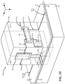
- FIGS. 2A-2D are simplified, diagrammatical, perspective sketches of a cooling structure according to the disclosure.
- FIG. 2A ′ is an enlarged portion of the cooling structure shown in FIG. 2A , such portion being enclosed by the arrow labelled 2 A′- 2 A′ in FIG. 2A , according to the disclosure;
- FIG. 3A is a schematic block diagram of a circuit formed on a thermal heat spreader of the cooling structure of FIGS. 2A-2D according to the disclosure;
- FIG. 3B is a simplified, diagrammatical sketch the cooling structure of FIGS. 2A-2D according to the disclosure.
- FIG. 4 is an exploded, perspective diagrammatical sketch of the thermal heat spreader of FIGS. 3A and 3B , with portions of one of the e elements thereof being partially broken away to show a portion of a bottom surface of such element of the thermal heat spreader of the cooling structure of FIGS. 2A-2D according to the disclosure;
- FIG. 5 is an exploded, diagrammatical perspective view sketch, of the cooling structure of FIGS. 2A-2D according to the disclosure
- FIGS. 6A-6D are simplified, side elevation views of the cooling structure of FIGS. 2A-2D according to the disclosure showing heat flow through the cooling structure of FIGS. 2A-2D according to the disclosure;
- FIGS. 7A and 7B together is a flow diagrams of the process used to form the cooling structure of FIGS. 2A-2D according to the disclosure;
- FIG. 8 through FIG. 12D are diagrammatical sketches useful in understand the process used to form the cooling structure of FIGS. 2A-2D ;
- FIGS. 13A and 13B are diagrammatical, cross-sectional sketches of a portion of the cooling structure of FIGS. 2A-2D showing the process used to electrically interconnect a microwave transmission line of the heat spreader of FIG. 4 with an exemplary one of an electrical component, partially broken, attached to a side of the heat spreader at various steps in such process according to the disclosure;
- FIG. 14 is schematic block diagram of an H-bridge circuit adapted for configuration on four sides of a heat spreader according to the disclosure.
- FIGS. 14A and 14B are simplified, diagrammatical, perspective sketches of a cooling structure according to the disclosure.
- a cooling structure 10 for cooling active, heat generating electrical components here for example, a pair of Field Effect Transistor (FET) MMIC power amplifiers 12 a , 12 b connected between passive circuits, or electrical components, here for example, a power splitter 14 and a power combiner 16 , by microwave transmission lines 17 a , 17 b , respectively, and microwave transmission lines 17 c , 17 d , respectively, as shown, to form a portion of the electrical circuit 18 , as shown in FIG. 3 .
- FET Field Effect Transistor
- the MMIC power amplifiers 12 a , 12 b , power splitter 14 , power combiner 16 and microwave transmission lines 17 a , 17 b , 17 c and 17 d are disposed on a heat spreader 24 , to be described and shown in more detail in FIG. 4 . It is to be noted here, however, that the pair of MMIC power amplifiers 12 a , 12 b are thermally coupled to a heatsink/cold plate 19 of the cooling structure 10 through a thermally coupled heat spreader 24 to be described in more detail in connection with FIG. 4 .
- the power splitter 14 is a conventional four-port power splitter, disposed on. SIDE 1 of the heat spreader 24 , for having: one port fed by an RF input signal on transmission line 17 e , a second port connected to conventional matched impedance terminator 20 a , disposed on SIDE 1 of the heat spreader 24 , through microwave transmission line 17 f ; and a pair of output ports, each one being coupled to a corresponding one of a pair of the pair of MMIC power amplifiers 12 a , 12 b , disposed on opposites SIDE 2 and SIDE 4 , respectively, of the heat spreader 24 , through the pair of microwave transmission lines 17 a , 17 b , respectively, as shown.
- each one of the MMIC power amplifiers 12 a , 12 b is coupled as inputs to the conventional four-port power combiner 16 , disposed on SIDE 3 of the heat spreader 24 , here a conventional four-port power combiner 16 (here also disposed on the heat spreader 24 ), having a pair of output ports through the microwave transmission lines 17 c , 17 d , respectively, as shown; one of the pair of output ports providing an RF output signal on microwave transmission line 17 g and the other being connected to a conventional matched terminator 20 b , disposed on SIDE 3 of the heat spreader 24 , through microwave transmission line 17 h , as shown.
- the microwave transmission lines 17 a - 17 h are microstrip transmission lines.
- a bottom portion of the heat spreader 24 passes through an opening 29 in a printed circuit board 13 having: a dielectric substrate 22 and a ground plane conductor 23 on a bottom surface of the substrate 22 .
- the printed circuit board 13 has formed on the upper surface thereof: a transmission line 17 e ′ which is connected to a microwave transmission line 17 e ′′ formed on side 1 of the heat spreader 24 , the transmission line 17 e ′ and connected transmission line 17 e ′′ forming the input transmission line 17 e , and a transmission line 17 g ′ which connects to a microwave transmission line 17 g ′′ formed on side 3 of the heat spreader 24 , the transmission line 17 g ′ and connected transmission line 17 g ′′ forming the input transmission line 17 g.
- the bottom portion of the heat spreader 24 passes through the opening 29 in the printed circuit board 13 onto a bottom surface 31 of a cavity 15 formed an portion of an upper surface 33 of a cold plate 19 .
- a suitable thermal interface material such as solder or thermally conductive adhesive 53 ( FIGS. 2A, 2A ′) is used to bond the upper surface 33 of the cold plate to the ground plane conductor 23 and the bottom surface of the heat spreader 24 and lower portions of the sidewalls to the heat spreader 24 to the sidewalls and bottom surface of the of the cavity 15 , as shown in FIG.
- microstrip transmission lines 17 e and 17 g ′ are formed on the printed circuit board 13 by strip conductors 21 a disposed on portions of the upper surface of the dielectric substrate 22 and a ground plane conductor 23 disposed on the bottom surface of the dielectric substrate 22 .
- the heat spreader 24 here in this example, is a three-dimensional, thermally conductive support structure, multi-sided, here in this example, a six-sided structure, and is shown in more detail in FIG. 4 having a six-sided thermally anisotropic material 28 , here for example pyrolytic graphite, having basal planes, indicated by dashed lines 30 disposed, in this example, in the Y-Z plane, that is, in this example, perpendicular to the upper surface 32 and the bottom surface 34 of the thermally anisotropic material 28 .
- heat spreader 24 has anisotropic heat conducting properties for conducting heat therethrough along preferred planes (the basal planes 30 ).
- the four vertical sides (Side 1 , Side 2 , Side 3 and Side 4 ) of the heat spreader 24 , and the thermally anisotropic material 28 are rectangular is shape, here longer along the Z-axis than along either the X-axis or Y-axis. It should be understood that other shapes may be used, for example, they may have more or less than four sides, further, the bottom portion of the heat spreader 24 , and the thermally anisotropic material 28 may be tapered. Further, as will be described in more detail below, the basal planes 30 intersect the bottom surface having the ground plane 51 of the heat generating MMIC power amplifiers 12 a , 12 b , here at ninety degree angles.
- the basal planes 30 may be in the X-Z plane, or one portion of the basal planes may be in the Y-Z plane and another portion may be in the X-Z plane.
- the heat spreader 24 includes a thermally and electrically conductive material 36 , here for example a metal, such as copper, serves as an encasing material, sometimes referred to herein as an encapsulation material 36 , to encase all six outer surfaces (top, bottom and four sides) of the thermally anisotropic material 28 . More particularly, the six outer surface of the thermally anisotropic material 28 are brazed to the thermally conductive material 36 with a suitable brazing material 38 , here for example, CuSil an alloy of 72% silver and 28% copper ( ⁇ 1%) marketed by Morgan. Advanced Materials, Quadrant 55-57 High Street Windsor Berkshire, United Kingdom, SL4 1LP; a eutectic alloy primarily used for vacuum brazing.
- a suitable brazing material 38 here for example, CuSil an alloy of 72% silver and 28% copper ( ⁇ 1%) marketed by Morgan. Advanced Materials, Quadrant 55-57 High Street Windsor Berkshire, United Kingdom, SL4 1LP; a eutectic
- thermally anisotropic material 28 In another method of attachment, no external bonding agent is used between thermally anisotropic material 28 and thermally conductive material 36 ; for example using; heat and pressure, such as thereto-compression bonding or hot isostatic pressing, for example,
- the thermally conductive material 36 is an encapsulating material used to encapsulate the thermally anisotropic material 28 and is sometimes also referred to herein as encapsulation material 36 .
- the surface of the encapsulation material 36 in contact with the MIMIC power amplifiers 12 a , 12 b can be made out of a high-thermal conductivity, but low CTE metal, such as Tungsten (4 PPM/° C.), Molybdenum (5.5 PPM/° C.), an alloy of Copper-Tungsten (5-10 PPM/° C.), an alloy of Copper-Molybdneum (6-10 PPM/° C.), or other such materials.
- this surface of material 36 in contact with the MMIC power amplifiers 12 a , 12 b can be made out of a ceramic, for example, Aluminum-Nitride (4.5 PPM/° C.), or Silicon Nitride (3.5 PPM/° C.), or others, which also have high thermal conductivity and a lower GTE.
- an attachment surface that is, the surface of encapsulation material 36 in contact with the MMIC power amplifiers 12 a , 12 b has a lower GTE, as compared to metal like Copper (18 PPM/° C.). Since the MMIC power amplifiers 12 a , 12 b , here have a substrate 50 ( FIGS.
- 6C, 6D made of, for example, Silicon Carbide, which has a lower CTE (2.8 PPM/° C.), the use of a high thermal conductivity with low CTE material on the top surface of encapsulation material 36 provides good thermal transport with improved CTE matching between the substrate 50 of the MMIC power amplifier 12 a , 12 b and the underlying heat spreader structure 24 .
- a higher degree of CTE matching between the substrate 50 of the MMIC power amplifier 12 a , 12 b and the underlying heat spreader structure 24 thus achieved, reduces thermal-induced stresses in the substrate 50 of the MMIC power amplifier 12 a , 12 b when the cooling structure 10 is exposed to temperature excursions during operation.
- improved GTE matching improves the mechanical reliability of the cooling structure 10 by lowering them tab-induced stresses.
- Better degree of GTE matching thus achieved, also helps increase the choice of materials available to be used for the Thermal interface Materials (TIM) (e.g. solder), here layer 48 a , ( FIGS. 6C and 6D ) and to be described in more detail in connection with FIGS. 9A through 12D used to attach a ground plane 51 ( FIGS. 6C and 6D ) on the bottom of the substrate 50 of the MMIC power amplifier 12 a , 12 b to the heat spreader 24 because TIM layer 43 a stresses are lowered.
- TIM Thermal interface Materials
- TIM layer 48 a because, being disposed between the substrate 50 of the MMIC power amplifier 12 a , 12 b and the surfaces of the encapsulation material 36 of heat spreader 24 , thermally coupled to the MMIC power amplifier 12 a , 12 b they would now be subjected to higher thermal-induced stresses.
- the encapsulation layer material 36 can be of Copper (18 PPM/° C.) and can be perfectly CTE-matched to the heat sink/cold plate 19 also made of copper.
- improved CTE matching is achieved on all sides of the spreader 24 by employing a combination of encapsulation materials rather than one single material. It is also possible to employ different materials for all or some of the remaining sides, as dictated by the CTE matching and thermal transfer needs of a given application.
- all or any of the six encapsulating sides can be made out of a metal or a non-metal, as noted above. If non-metal then the added step of writing the ground plane precedes writing the dielectric.
- the power splitter 14 and power combiner 16 are also bonded to the heat spreader 24 using a TIM e layer 48 b ( FIGS. 6A and 6B ).
- the terminators 20 a , 20 b are also bonded to the heat spreader 24 using a TIM layer 48 c ( FIGS. 6A and 6B ).
- the microwave transmission lines 17 a - 17 g arc here microstrip transmission lines with portions of such lines being bonded to the heat spreader.
- the TIM layer 48 a , 48 b and 48 c may be different bonding material CTEs.
- the basal planes 30 are parallel to sides 2 and 4 and perpendicular to sides 1 and 3 and hence perpendicular to the bottom surfaces of the power amplifiers 12 a and 12 b .
- the heat low from the power amplifiers 12 a , 12 b to the heat sink/cold plate 19 is shown by the arrows 61 in FIGS. 6A-6D .
- a device region R 1 reference FIG.
- the power splitter 14 and power combiner 16 components have passive device regions R 2 (reference FIG. 2 ) having for example, microwave transmission lines arranged to form such power splitter 14 and power combiner 16 in any conventional manner.
- the terminators 20 a , 20 b have passive devices, such as resistors, arranged in any conventional manner to provide proper impedance machining termination components.
- the bottom portion of the heat spreader 24 passes through an opening 29 in the printed circuit board 13 onto the bottom surface of a cavity 15 formed a portion of an upper surface of a cold plate 19 .
- a small gap 60 is left between the ends of the microwave transmission lines 17 e ′, 17 g ′ on the printed circuit board 13 and the bottom portion of the heat spreader 24 .
- This gap 60 is filled by injection into the upper portion of the gap 60 with an elastic dielectric material 63 , such as a silicone material, as shown.
- Next bridging strip conductor 64 is printed onto the dielectric material 63 to electrically interconnect the strip conductor 21 a on the printed circuit board 13 of the microwave transmission lines 17 e ′, 17 g ′ of the dielectric substrate 22 to the strip conductor 21 b ( FIG. 5 ) of the microwave transmission lines 17 e ′′, 17 g ′′ on the heat spreader 24 and thereby form transmission line 17 e , 17 g as described above.
- the conductive encapsulation material 36 is electrically and thermally connected to the heat sink 197 and therefore to the ground plane conductor 23 of the printed circuit board 13 .
- other passive elements in addition to directional couplers and power divider/combiners, such as resistors, capacitors, and inductors, for example, may be formed on the sides of the heat spreader 24 using dielectric material and conductive material arranged appropriately to form such passive devices.
- a resistive material may then be printed over the dielectric material printed and cured on the conductive encapsulation material 36 in a region where a resistor is to be formed with one end of the resistive material being connected to a strip conductor of a microwave transmission line and the other end being connected to a printed strip, conductor that passes over the edge of the dielectric material to the conductive encapsulation material 36 , which as noted above, is electrically connected to the ground plane conductor 23 .
- the terminators 20 a , 20 b may be such a resistor having an impedance to provide a matched load for the electrical circuit 18 ( FIGS. 3A, 3B ).
- FIG. 7 a flow diagram of the process used to form the cooling structure 10 , FIGS. 2A-2D is shown. It is first noted that the process may be performed using computer controlled Additive Manufacturing (AM) or 3D printed processes.
- the heat spreader 24 is formed ( FIG. 8 ), Step 100 .
- the MMIC power amplifiers 12 a , 12 b , splitter 14 and combiner 16 are attached to sides of the formed heat spreader 24 with TIM 48 a with the ground plane conductors 51 as described above in connection with FIGS. 6C and 6D ( FIGS. 9A-9D ) Step 200 .
- ground plane conductors 51 of the MMIC power amplifiers 12 a , 12 b are perpendicular to the basal planes 30 while the ground plane conductors 51 of the splitter 14 and combiner 16 are parallel to the basal planes 30 , see FIGS. 6A-6D ,
- a dielectric material 71 is printed and then cured over the heat spreader 24 in regions exposed by the attached MMIC power amplifiers 12 a , 12 b , splitter 14 , combiner 16 and terminators 20 a , 20 b and also leaving the lower and bottom portions of the heat spreader 24 uncovered thereby leaving the encapsulating material 36 exposed on the lower and bottom portions of the heat spreader 24 ( FIGS. 10A-10D ), Step 300 .
- a dielectric material 73 is printed and then cure to till any seam, or small space 57 ( FIG. 13A ), that may exist between the cured dielectric material 71 and the components: the MMIC power amplifiers 12 a , 12 b ; splitter 14 ; and combiner 16 , and terminators 20 a , 20 b , as shown in FIGS. 13A and 13 B for an exemplary one of the components, here for example, the MMIC power amplifier 12 a , ( FIGS. 11A-11D ).
- Step 400 Strip conductors 21 b ( FIGS.
- the dielectric material ' 73 has a low Young's modulus (an elastic dielectric material such as, for example, silicone). The Young's modulus is selected to enable expansion and contraction of such elements over the temperature operating and storage range without resulting in breakage of electrical interconnect passing over such gap filling materials.
- Form the input and output microwave transmission lines interconnects 17 e ′, 17 g ′ are on printed circuit board 13 , such printed circuit board 13 having the opening 29 passing through it for receiving the lower portion 92 ( FIGS. 5, 12A-12D ) of the heat spreader 24 , Step 600 .
- the cold plate 19 is formed with the cavity 15 in the upper surface, Step 700 .
- a thermal interface material (TIM) 53 here for example solder, is applied to the upper surface of the cold plate 19 and to the sidewalls and bottom of cavity 15 in cold plate 19 ( FIG. 2A ′), Step 800 .
- the lower portion 92 ( FIGS. 5, 12A-12D ) of the heat spreader 24 is inserted through the opening 29 in the printed circuit board 13 onto the bottom surface of the cavity 15 in the cold plate 19 .
- FIG. 2A ′ that vertical edges of the opening 29 in the printed circuit board 13 are spaced from the encapsulating material 36 on the sides of the lower portions 92 of the heat spreader 24 thereby leaving a gap 60 between the vertical edges of the printed circuit board 13 and the encapsulating material 36 , Step 900 . It is noted in FIG.
- thermal interface material (TIM) 53 is applied below the level of strip conductors of the input and output microwave transmission lines interconnects 17 e ′, 17 g ′ and the TIM 53 is used to bond the encapsulating material 36 to the sidewalls and bottom surface of the heat spreader 24 to the sidewalls and bottom of the cavity 15 and also bond the printed circuit board 13 (the ground plane conductor 23 ( FIG. 2A ′) to the upper surface of the cold plate 19 by reflow or curing, Step 1000 .
- a dielectric material 63 ( FIG. 2A ′) having a low Young's modulus (an elastic dielectric material such as, for example, silicone) is printed and then cured in the gap 60 above the thermal interface material (TIM) 53 ( FIG.
- Step 1100 The Young' s modulus is selected to enable expansion and contraction of such elements over the temperature operating and storage range without resulting in breakage of electrical interconnect passing over such seam or bridge gap filling materials.
- Bridging strip conductors 64 are printed and then cured over portions of strip conductors of the microwave transmission lines 17 e ′, 17 g ′ on dielectric substrate 22 and cured over portions of strip conductors of the microwave transmission lines 17 e ′′, 17 g ′′ on the dielectric material 71 to electrically interconnect the input and output microwave transmission lines 17 e , 17 g on the printed circuit board 13 with the microwave transmission lines 17 e , 17 g on the heat spreader 24 and thereby complete the circuit 18 , Step 1200 .
- CTEs Coefficients of Thermal Expansions
- dielectric filling materials used to fill gaps and seams between elements should have sufficient elasticity (Young's modulus) to enable expansion and contraction of such elements over the temperature operating and storage range without resulting in breakage of electrical interconnect passing over such seam or bridge gap filling materials.
- transmissions and splitter, combiner or other matching networks and accompanying bias networks may be realized on the structure 24 in a number of ways.
- Dielectric materials may be additively printed using paste or filament and the strip conductors on the heat spreader 24 may be printed using AM or 3D printing.
- the circuit may be formed on a flexible, conformable substrate and then bonded to the structure 24 with a suitable TIM.
- the microwave transmission lines 17 a - 17 h may be formed using, for example, computer controlled Additive Manufacturing (AM) or 3D printing, for example.
- bias control lines including lines +V, ⁇ V ( FIGS. 2A-2D ) for supplying voltages to the MMIC amplifiers 12 a , 12 b may also be printed on dielectric layer 71 on the same or additional layers of dielectric 71 .
- terminators 20 a , 20 b have been shown and described as being on sides 1 and 3 , respectively, they may be on sides 2 and 4 , respectively, and with transmission lines 17 f and 17 h , respectively having portions on sides 1 and 4 , and sides 3 and 2 , respectively.
- the sides having the heat generating elements of the circuit need not be disposed in planes that are perpendicular (ninety degrees) to bottom surface of the substrate of the power MMIC amplifiers 12 a , 12 b but may be in planes that intersect the bottom surface of the substrate of the heat generating elements heat generating elements of the circuit at other angles than ninety degrees, such as, for example, 45 degrees or 30 degrees.
- the splitter 14 and combiner 16 are described above as being individual passive components that are bonded to the heat spreader 24 they may be formed with strip conductors in the same manner as the transmissions lines on the dielectric material 71 formed over the portion of the surface of the heat spreader 24 where such splitter 14 and combiner 16 individual components are now located.
- strip conductors on the heat spreader 24 and components on the heat spreader 24 may be made with ribbon or wire bonds.
- the disclosure may be used with other applications than to splitting and combining networks and in power applications such as, for example, H-bridge designs, for example, see FIGS. 14, 14A and 14B where Metal Oxide Semiconductor Field Effect Transistors (MOSFETs) Q 1 -Q 4 are connected to diodes D 1 -D 4 , as shown in FIG. 14 .
- MOSFETs Metal Oxide Semiconductor Field Effect Transistors
- MOSFETs Q 1 -Q 2 and diodes D 1 -D 2 are bonded and thermally coupled to side 2 of the spreader 24 and that the MOSFETs Q 3 -Q 4 and diodes D 3 -D 3 are bonded and thermally coupled to opposite side 4 spreader 24 , such sides 2 and 4 being perpendicular to the basal planes 30 of the spreader 24 , FIG. 4 , FIGS. 14, 14A and 14B .
Landscapes
- Engineering & Computer Science (AREA)
- Microelectronics & Electronic Packaging (AREA)
- Power Engineering (AREA)
- Physics & Mathematics (AREA)
- Computer Hardware Design (AREA)
- General Physics & Mathematics (AREA)
- Condensed Matter Physics & Semiconductors (AREA)
- Chemical & Material Sciences (AREA)
- Materials Engineering (AREA)
- Manufacturing & Machinery (AREA)
- Geometry (AREA)
- Ceramic Engineering (AREA)
- Cooling Or The Like Of Semiconductors Or Solid State Devices (AREA)
- Cooling Or The Like Of Electrical Apparatus (AREA)
- Waveguides (AREA)
Abstract
Description
Claims (5)
Priority Applications (7)
| Application Number | Priority Date | Filing Date | Title |
|---|---|---|---|
| US15/948,404 US10785863B2 (en) | 2018-04-09 | 2018-04-09 | Circuit support and cooling structure |
| PL19717033.5T PL3776648T3 (en) | 2018-04-09 | 2019-03-26 | Circuit support and cooling structure |
| SG11202009487QA SG11202009487QA (en) | 2018-04-09 | 2019-03-26 | Circuit support and cooling structure |
| KR1020207032039A KR102250940B1 (en) | 2018-04-09 | 2019-03-26 | Circuit support and cooling structure |
| PCT/US2019/023988 WO2019199443A1 (en) | 2018-04-09 | 2019-03-26 | Circuit support and cooling structure |
| EP19717033.5A EP3776648B1 (en) | 2018-04-09 | 2019-03-26 | Circuit support and cooling structure |
| JP2020555214A JP7072669B2 (en) | 2018-04-09 | 2019-03-26 | Circuit support and cooling structure |
Applications Claiming Priority (1)
| Application Number | Priority Date | Filing Date | Title |
|---|---|---|---|
| US15/948,404 US10785863B2 (en) | 2018-04-09 | 2018-04-09 | Circuit support and cooling structure |
Publications (2)
| Publication Number | Publication Date |
|---|---|
| US20190313522A1 US20190313522A1 (en) | 2019-10-10 |
| US10785863B2 true US10785863B2 (en) | 2020-09-22 |
Family
ID=66102769
Family Applications (1)
| Application Number | Title | Priority Date | Filing Date |
|---|---|---|---|
| US15/948,404 Active 2038-09-06 US10785863B2 (en) | 2018-04-09 | 2018-04-09 | Circuit support and cooling structure |
Country Status (7)
| Country | Link |
|---|---|
| US (1) | US10785863B2 (en) |
| EP (1) | EP3776648B1 (en) |
| JP (1) | JP7072669B2 (en) |
| KR (1) | KR102250940B1 (en) |
| PL (1) | PL3776648T3 (en) |
| SG (1) | SG11202009487QA (en) |
| WO (1) | WO2019199443A1 (en) |
Cited By (1)
| Publication number | Priority date | Publication date | Assignee | Title |
|---|---|---|---|---|
| US10916524B2 (en) * | 2016-12-29 | 2021-02-09 | Intel Corporation | Stacked dice systems |
Families Citing this family (10)
| Publication number | Priority date | Publication date | Assignee | Title |
|---|---|---|---|---|
| US11152279B2 (en) | 2018-03-26 | 2021-10-19 | Raytheon Company | Monolithic microwave integrated circuit (MMIC) cooling structure |
| US11075141B2 (en) | 2018-09-14 | 2021-07-27 | Raytheon Company | Module base with integrated thermal spreader and heat sink for thermal and structural management of high-performance integrated circuits or other devices |
| US10896861B2 (en) * | 2019-04-22 | 2021-01-19 | Raytheon Company | Heterogeneous multi-layer MMIC assembly |
| WO2020218326A1 (en) * | 2019-04-23 | 2020-10-29 | 京セラ株式会社 | Wiring board, electronic device, and electronic module |
| US11545297B2 (en) * | 2019-06-06 | 2023-01-03 | Toyota Motor Engineering & Manufacturing North America, Inc. | Functionally graded thermal vias for inductor winding heat flow control |
| US11252811B2 (en) * | 2020-01-15 | 2022-02-15 | Cisco Technology, Inc. | Power distribution from point-of-load with cooling |
| US11032947B1 (en) | 2020-02-17 | 2021-06-08 | Raytheon Company | Tailored coldplate geometries for forming multiple coefficient of thermal expansion (CTE) zones |
| US11406007B2 (en) | 2020-02-19 | 2022-08-02 | Raytheon Company | Radio frequency (RF) energy transmission line transition structure |
| EP4307338A1 (en) * | 2022-07-12 | 2024-01-17 | Comet AG | Radio frequency generator |
| US20240121919A1 (en) * | 2022-10-06 | 2024-04-11 | Ciena Corporation | Method and apparatus for managing heat distribution in a semiconductor device |
Citations (43)
| Publication number | Priority date | Publication date | Assignee | Title |
|---|---|---|---|---|
| US3156091A (en) | 1961-07-19 | 1964-11-10 | Curtiss Wright Corp | Multi-layer anisotropic heat shield construction |
| US3980105A (en) | 1974-07-10 | 1976-09-14 | Hitco | Laminated article comprising pyrolytic graphite and a composite substrate therefor |
| US4057610A (en) | 1975-07-25 | 1977-11-08 | Monsanto Company | Hose reinforced with discontinuous fibers oriented in the radial direction |
| US4627472A (en) | 1978-07-31 | 1986-12-09 | Monsanton Company | Hose reinforced with discontinuous fibers oriented in the radial direction |
| US4672472A (en) | 1984-02-13 | 1987-06-09 | Victor Company Of Japan, Ltd. | Playback apparatus for audiovisual disc records |
| US5241450A (en) * | 1992-03-13 | 1993-08-31 | The United States Of America As Represented By The United States Department Of Energy | Three dimensional, multi-chip module |
| US5434362A (en) * | 1994-09-06 | 1995-07-18 | Motorola, Inc. | Flexible circuit board assembly and method |
| US5545924A (en) * | 1993-08-05 | 1996-08-13 | Honeywell Inc. | Three dimensional package for monolithic microwave/millimeterwave integrated circuits |
| US6075701A (en) | 1999-05-14 | 2000-06-13 | Hughes Electronics Corporation | Electronic structure having an embedded pyrolytic graphite heat sink material |
| JP2001267441A (en) | 2000-03-15 | 2001-09-28 | Kyocera Corp | Package for containing semiconductor element |
| US20020006523A1 (en) | 2000-07-07 | 2002-01-17 | Obeshaw Dale Francis | Structural members containing vibration damping mechanisms and methods for making the same |
| US6387462B1 (en) | 1999-12-10 | 2002-05-14 | Ucar Graph-Tech Inc. | Thermal insulating device for high temperature reactors and furnaces which utilize highly active chemical gases |
| US20020167800A1 (en) | 2001-05-02 | 2002-11-14 | Smalc Martin D. | Radial Finned Heat Sink |
| US20030042153A1 (en) | 2001-08-31 | 2003-03-06 | Farrar Paul A. | Multiple chip stack structure and cooling system |
| US20030116312A1 (en) | 2001-12-13 | 2003-06-26 | Krassowski Daniel W. | Heat dissipating component using high conducting inserts |
| US6674347B1 (en) | 1999-03-23 | 2004-01-06 | Nec Corporation | Multi-layer substrate suppressing an unwanted transmission mode |
| US6717813B1 (en) | 2003-04-14 | 2004-04-06 | Thermal Corp. | Heat dissipation unit with direct contact heat pipe |
| US7005584B2 (en) * | 2004-02-13 | 2006-02-28 | Honeywell International Inc. | Compact navigation device assembly |
| US20060096740A1 (en) | 2004-11-10 | 2006-05-11 | Wen-Chun Zheng | Nearly isothermal heat pipe heat sink and process for making the same |
| US20070053168A1 (en) | 2004-01-21 | 2007-03-08 | General Electric Company | Advanced heat sinks and thermal spreaders |
| EP1783833A2 (en) | 2005-11-04 | 2007-05-09 | Advanced Energy Technology Inc. | Heat Spreaders with Vias |
| US20070115076A1 (en) * | 2005-11-21 | 2007-05-24 | Harris Corporation | High density three-dimensional RF / microwave switch architecture |
| US20070262836A1 (en) * | 2006-04-26 | 2007-11-15 | Ems Technologies, Inc. | Planar mixed-signal circuit board |
| US20090066420A1 (en) * | 2007-09-12 | 2009-03-12 | Viasat, Inc. | Solid state power amplifier with multi-planar mmic modules |
| US20090091892A1 (en) * | 2007-09-26 | 2009-04-09 | Rohm Co., Ltd. | Semiconductor Device |
| US20100177796A1 (en) | 2009-01-09 | 2010-07-15 | Newport Corporation | Laser device and heat sink with core to manage stress due to thermal expansion |
| WO2011008467A1 (en) | 2009-07-14 | 2011-01-20 | Specialty Minerals (Michigan) Inc. | Anisotropic thermal conduction element and manufacturing method |
| US20110030924A1 (en) | 2003-09-12 | 2011-02-10 | The Furukawa Electric Co., Ltd. | Heat sink with heat pipes and method for manufacturing the same |
| US20120063097A1 (en) * | 2010-09-10 | 2012-03-15 | Raytheon Company | Monolithic microwave integrated circuit |
| DE102011078674A1 (en) | 2011-07-05 | 2013-01-10 | Siemens Aktiengesellschaft | cooling component |
| US20130092354A1 (en) | 2011-10-18 | 2013-04-18 | Thermal Corp. | Heat pipe having a wick with a hybrid profile |
| US20130208434A1 (en) * | 2012-02-10 | 2013-08-15 | Raytheon Company | FLIP-CHIP MOUNTED MICROSTRIP MONOLITHIC MICROWAVE INTEGRATED CIRCUITS (MMICs) |
| US20130271905A1 (en) * | 2002-10-22 | 2013-10-17 | Jason A. Sullivan | Systems and methods for providing dynamic computing systems |
| US20150062802A1 (en) | 2013-09-05 | 2015-03-05 | Dell Products, L.P. | Heat pipe assemblies |
| US9093442B1 (en) * | 2013-03-15 | 2015-07-28 | Lockheed Martin Corporation | Apparatus and method for achieving wideband RF performance and low junction to case thermal resistance in non-flip bump RFIC configuration |
| US9318450B1 (en) | 2014-11-24 | 2016-04-19 | Raytheon Company | Patterned conductive epoxy heat-sink attachment in a monolithic microwave integrated circuit (MMIC) |
| US20160316570A1 (en) * | 2014-01-02 | 2016-10-27 | Koninklijke Philips N.V. | Method for manufacturing a non-planar printed circuit board assembly |
| US20170042058A1 (en) * | 2015-08-03 | 2017-02-09 | Apple Inc. | Parallel heat spreader |
| US20170100907A1 (en) | 2015-10-09 | 2017-04-13 | Raytheon Company | Anisotropic thermal conduit |
| US20170284647A1 (en) * | 2016-03-31 | 2017-10-05 | Osram Sylvania Inc. | Flexible interconnection between substrates and a multi-dimensional light engine using the same |
| US20170325332A1 (en) * | 2016-05-04 | 2017-11-09 | Northrop Grumman Systems Corporation | Bridging electronic inter-connector and corresponding connection method |
| US9978698B1 (en) * | 2017-01-25 | 2018-05-22 | Raytheon Company | Interconnect structure for electrical connecting a pair of microwave transmission lines formed on a pair of spaced structure members |
| US20190295918A1 (en) | 2018-03-26 | 2019-09-26 | Raytheon Company | Monolithic microwave integrated circuit (mmic) cooling structure |
Family Cites Families (4)
| Publication number | Priority date | Publication date | Assignee | Title |
|---|---|---|---|---|
| US20020157819A1 (en) * | 2001-04-04 | 2002-10-31 | Julian Norley | Graphite-based thermal dissipation component |
| KR100586698B1 (en) | 2003-12-23 | 2006-06-08 | 삼성전자주식회사 | Semiconductor Module having semiconductor chip package which is vertically mounted on module board |
| JP2010129806A (en) | 2008-11-28 | 2010-06-10 | Mitsubishi Electric Corp | Power semiconductor device and process of manufacturing the same |
| US10347559B2 (en) | 2011-03-16 | 2019-07-09 | Momentive Performance Materials Inc. | High thermal conductivity/low coefficient of thermal expansion composites |
-
2018
- 2018-04-09 US US15/948,404 patent/US10785863B2/en active Active
-
2019
- 2019-03-26 WO PCT/US2019/023988 patent/WO2019199443A1/en unknown
- 2019-03-26 SG SG11202009487QA patent/SG11202009487QA/en unknown
- 2019-03-26 JP JP2020555214A patent/JP7072669B2/en active Active
- 2019-03-26 EP EP19717033.5A patent/EP3776648B1/en active Active
- 2019-03-26 KR KR1020207032039A patent/KR102250940B1/en active IP Right Grant
- 2019-03-26 PL PL19717033.5T patent/PL3776648T3/en unknown
Patent Citations (46)
| Publication number | Priority date | Publication date | Assignee | Title |
|---|---|---|---|---|
| US3156091A (en) | 1961-07-19 | 1964-11-10 | Curtiss Wright Corp | Multi-layer anisotropic heat shield construction |
| US3980105A (en) | 1974-07-10 | 1976-09-14 | Hitco | Laminated article comprising pyrolytic graphite and a composite substrate therefor |
| US4057610A (en) | 1975-07-25 | 1977-11-08 | Monsanto Company | Hose reinforced with discontinuous fibers oriented in the radial direction |
| US4627472A (en) | 1978-07-31 | 1986-12-09 | Monsanton Company | Hose reinforced with discontinuous fibers oriented in the radial direction |
| US4672472A (en) | 1984-02-13 | 1987-06-09 | Victor Company Of Japan, Ltd. | Playback apparatus for audiovisual disc records |
| US5241450A (en) * | 1992-03-13 | 1993-08-31 | The United States Of America As Represented By The United States Department Of Energy | Three dimensional, multi-chip module |
| US5545924A (en) * | 1993-08-05 | 1996-08-13 | Honeywell Inc. | Three dimensional package for monolithic microwave/millimeterwave integrated circuits |
| US5434362A (en) * | 1994-09-06 | 1995-07-18 | Motorola, Inc. | Flexible circuit board assembly and method |
| US6674347B1 (en) | 1999-03-23 | 2004-01-06 | Nec Corporation | Multi-layer substrate suppressing an unwanted transmission mode |
| US6075701A (en) | 1999-05-14 | 2000-06-13 | Hughes Electronics Corporation | Electronic structure having an embedded pyrolytic graphite heat sink material |
| US6387462B1 (en) | 1999-12-10 | 2002-05-14 | Ucar Graph-Tech Inc. | Thermal insulating device for high temperature reactors and furnaces which utilize highly active chemical gases |
| JP2001267441A (en) | 2000-03-15 | 2001-09-28 | Kyocera Corp | Package for containing semiconductor element |
| US20020006523A1 (en) | 2000-07-07 | 2002-01-17 | Obeshaw Dale Francis | Structural members containing vibration damping mechanisms and methods for making the same |
| US20020167800A1 (en) | 2001-05-02 | 2002-11-14 | Smalc Martin D. | Radial Finned Heat Sink |
| US20030042153A1 (en) | 2001-08-31 | 2003-03-06 | Farrar Paul A. | Multiple chip stack structure and cooling system |
| US20030116312A1 (en) | 2001-12-13 | 2003-06-26 | Krassowski Daniel W. | Heat dissipating component using high conducting inserts |
| US20130271905A1 (en) * | 2002-10-22 | 2013-10-17 | Jason A. Sullivan | Systems and methods for providing dynamic computing systems |
| US6717813B1 (en) | 2003-04-14 | 2004-04-06 | Thermal Corp. | Heat dissipation unit with direct contact heat pipe |
| US20110030924A1 (en) | 2003-09-12 | 2011-02-10 | The Furukawa Electric Co., Ltd. | Heat sink with heat pipes and method for manufacturing the same |
| US20070053168A1 (en) | 2004-01-21 | 2007-03-08 | General Electric Company | Advanced heat sinks and thermal spreaders |
| US7005584B2 (en) * | 2004-02-13 | 2006-02-28 | Honeywell International Inc. | Compact navigation device assembly |
| US20060096740A1 (en) | 2004-11-10 | 2006-05-11 | Wen-Chun Zheng | Nearly isothermal heat pipe heat sink and process for making the same |
| US7303005B2 (en) | 2005-11-04 | 2007-12-04 | Graftech International Holdings Inc. | Heat spreaders with vias |
| EP1783833A2 (en) | 2005-11-04 | 2007-05-09 | Advanced Energy Technology Inc. | Heat Spreaders with Vias |
| US20070115076A1 (en) * | 2005-11-21 | 2007-05-24 | Harris Corporation | High density three-dimensional RF / microwave switch architecture |
| US20070262836A1 (en) * | 2006-04-26 | 2007-11-15 | Ems Technologies, Inc. | Planar mixed-signal circuit board |
| US20090066420A1 (en) * | 2007-09-12 | 2009-03-12 | Viasat, Inc. | Solid state power amplifier with multi-planar mmic modules |
| US20090091892A1 (en) * | 2007-09-26 | 2009-04-09 | Rohm Co., Ltd. | Semiconductor Device |
| US20100177796A1 (en) | 2009-01-09 | 2010-07-15 | Newport Corporation | Laser device and heat sink with core to manage stress due to thermal expansion |
| WO2011008467A1 (en) | 2009-07-14 | 2011-01-20 | Specialty Minerals (Michigan) Inc. | Anisotropic thermal conduction element and manufacturing method |
| US20120063097A1 (en) * | 2010-09-10 | 2012-03-15 | Raytheon Company | Monolithic microwave integrated circuit |
| DE102011078674A1 (en) | 2011-07-05 | 2013-01-10 | Siemens Aktiengesellschaft | cooling component |
| US20130092354A1 (en) | 2011-10-18 | 2013-04-18 | Thermal Corp. | Heat pipe having a wick with a hybrid profile |
| US20130208434A1 (en) * | 2012-02-10 | 2013-08-15 | Raytheon Company | FLIP-CHIP MOUNTED MICROSTRIP MONOLITHIC MICROWAVE INTEGRATED CIRCUITS (MMICs) |
| US9093442B1 (en) * | 2013-03-15 | 2015-07-28 | Lockheed Martin Corporation | Apparatus and method for achieving wideband RF performance and low junction to case thermal resistance in non-flip bump RFIC configuration |
| US20150062802A1 (en) | 2013-09-05 | 2015-03-05 | Dell Products, L.P. | Heat pipe assemblies |
| US20160316570A1 (en) * | 2014-01-02 | 2016-10-27 | Koninklijke Philips N.V. | Method for manufacturing a non-planar printed circuit board assembly |
| US9318450B1 (en) | 2014-11-24 | 2016-04-19 | Raytheon Company | Patterned conductive epoxy heat-sink attachment in a monolithic microwave integrated circuit (MMIC) |
| US20170042058A1 (en) * | 2015-08-03 | 2017-02-09 | Apple Inc. | Parallel heat spreader |
| US20170100907A1 (en) | 2015-10-09 | 2017-04-13 | Raytheon Company | Anisotropic thermal conduit |
| US9889624B2 (en) | 2015-10-09 | 2018-02-13 | Raytheon Company | Anisotropic thermal conduit |
| US10232582B2 (en) | 2015-10-09 | 2019-03-19 | Raytheon Company | Anisotropic thermal conduit |
| US20170284647A1 (en) * | 2016-03-31 | 2017-10-05 | Osram Sylvania Inc. | Flexible interconnection between substrates and a multi-dimensional light engine using the same |
| US20170325332A1 (en) * | 2016-05-04 | 2017-11-09 | Northrop Grumman Systems Corporation | Bridging electronic inter-connector and corresponding connection method |
| US9978698B1 (en) * | 2017-01-25 | 2018-05-22 | Raytheon Company | Interconnect structure for electrical connecting a pair of microwave transmission lines formed on a pair of spaced structure members |
| US20190295918A1 (en) | 2018-03-26 | 2019-09-26 | Raytheon Company | Monolithic microwave integrated circuit (mmic) cooling structure |
Non-Patent Citations (13)
| Title |
|---|
| Darwish et al.; Three Dimensional Transmission Lines and Power Divider Circuits. Apr. 1, 2009; 8 pages. |
| Final Office Action dated Dec. 10, 2019 for U.S. Appl. No. 15/935,622, 15 pages. |
| Final Office Action dated Sep. 28, 2018 for U.S. Appl. No. 15/870,155; 10 Pages. |
| Gries; Photonics Applied: Microelectronics Processing: Laser direct structuring creates low-cost 3D integrated circuits. Oct. 10, 2010; 6 pages. |
| International Search Report dated Jul. 2, 2019 for International Application No. PCT/US2019/023988; 5 Pages. |
| Notification of Transmittal of the International Search Report and the Written Opinion of the ISA dated Jul. 2, 2019 for International Application No. PCT/US2019/023988; 1 Page. |
| PCT International Search Report and Written Opinion dated Jan. 9, 2017 for International Application No. PCT/US2016/054290; 9 pages. |
| PCT Invitation to Pay Additional Fees and Partial Search Report dated Oct. 18, 2019 for International Application No. PCT/US2019/016282; 16 Pages. |
| Supplemental Response to Final Office Action with RCE dated Dec. 13, 2019 for U.S. Appl. No. 15/935,622, 19 pages. |
| Tehrani et al.; Inkjet-Printed 3D Interconnects for Millimeter-Wave System-on-Package Solutions. 2016 IEEE MTT-S International Microwave Symposium (IMS), San Francisco, CA; Jan. 1, 2016; 4 pages. |
| Terminal Disclaimer and Response to Office Action dated Sep. 28, 2018 for U.S. Appl. No. 15/870,155, filed Oct. 4, 2018; 11 Pages. |
| Whelan, et al.; GaN Technology for Radars. CS MANTECH Conference, Apr. 23-26, 2012, Boston, Massachusetts, USA. 4 pages. |
| Written Opinion of the ISA dated Jul. 2, 2019 for International Application No. PCT/US2019/023988; 12 Pages. |
Cited By (1)
| Publication number | Priority date | Publication date | Assignee | Title |
|---|---|---|---|---|
| US10916524B2 (en) * | 2016-12-29 | 2021-02-09 | Intel Corporation | Stacked dice systems |
Also Published As
| Publication number | Publication date |
|---|---|
| JP7072669B2 (en) | 2022-05-20 |
| KR102250940B1 (en) | 2021-05-11 |
| PL3776648T3 (en) | 2023-04-17 |
| KR20200133388A (en) | 2020-11-27 |
| JP2021518990A (en) | 2021-08-05 |
| WO2019199443A1 (en) | 2019-10-17 |
| EP3776648B1 (en) | 2023-01-04 |
| EP3776648A1 (en) | 2021-02-17 |
| SG11202009487QA (en) | 2020-10-29 |
| US20190313522A1 (en) | 2019-10-10 |
Similar Documents
| Publication | Publication Date | Title |
|---|---|---|
| US10785863B2 (en) | Circuit support and cooling structure | |
| JP7105981B2 (en) | Monolithic microwave integrated circuit (MMIC) cooling structure | |
| US7005734B2 (en) | Double-sided cooling isolated packaged power semiconductor device | |
| JP2004507073A (en) | High rigidity, multi-layer semiconductor package and manufacturing method thereof | |
| US6414847B1 (en) | Integral dielectric heatspreader | |
| EP1610381A2 (en) | Electronic package employing segmented connector and solder joint | |
| JP2009176839A (en) | Heat dissipation structure of semiconductor element | |
| JPS6329562A (en) | Integrated circuit package | |
| EP1255298A2 (en) | Power device with a plastic molded package and direct bonded substrate | |
| JP6906647B2 (en) | Semiconductor device | |
| CN108496248B (en) | Electronic chip device with improved thermal resistance and related manufacturing process | |
| JPH10256428A (en) | Semiconductor package | |
| JPH10256413A (en) | Semiconductor package | |
| JP6935976B2 (en) | Power modules and how to manufacture power modules | |
| JPH10256414A (en) | Semiconductor package | |
| JPH10275878A (en) | Semiconductor package | |
| WO2024132156A1 (en) | A design for enhancing the long term reliability of a large joining area in a power semiconductor module | |
| JPH08274225A (en) | Semiconductor component | |
| JOHNSON et al. | 10 WAFER-SCALE MULTICHIP | |
| JPH10275882A (en) | Semiconductor package | |
| JP2010212520A (en) | Electronic device and method of manufacturing the same |
Legal Events
| Date | Code | Title | Description |
|---|---|---|---|
| FEPP | Fee payment procedure |
Free format text: ENTITY STATUS SET TO UNDISCOUNTED (ORIGINAL EVENT CODE: BIG.); ENTITY STATUS OF PATENT OWNER: LARGE ENTITY |
|
| AS | Assignment |
Owner name: RAYTHEON COMPANY, MASSACHUSETTS Free format text: ASSIGNMENT OF ASSIGNORS INTEREST;ASSIGNORS:TRULLI, SUSAN C.;LAIGHTON, CHRISTOPHER M.;REEL/FRAME:045486/0572 Effective date: 20180409 |
|
| STPP | Information on status: patent application and granting procedure in general |
Free format text: DOCKETED NEW CASE - READY FOR EXAMINATION |
|
| STPP | Information on status: patent application and granting procedure in general |
Free format text: NON FINAL ACTION MAILED |
|
| STPP | Information on status: patent application and granting procedure in general |
Free format text: RESPONSE TO NON-FINAL OFFICE ACTION ENTERED AND FORWARDED TO EXAMINER |
|
| STPP | Information on status: patent application and granting procedure in general |
Free format text: FINAL REJECTION MAILED |
|
| STPP | Information on status: patent application and granting procedure in general |
Free format text: NOTICE OF ALLOWANCE MAILED -- APPLICATION RECEIVED IN OFFICE OF PUBLICATIONS |
|
| STPP | Information on status: patent application and granting procedure in general |
Free format text: PUBLICATIONS -- ISSUE FEE PAYMENT VERIFIED |
|
| STCF | Information on status: patent grant |
Free format text: PATENTED CASE |
|
| MAFP | Maintenance fee payment |
Free format text: PAYMENT OF MAINTENANCE FEE, 4TH YEAR, LARGE ENTITY (ORIGINAL EVENT CODE: M1551); ENTITY STATUS OF PATENT OWNER: LARGE ENTITY Year of fee payment: 4 |