JP7462013B2 - Display device - Google Patents
Display device Download PDFInfo
- Publication number
- JP7462013B2 JP7462013B2 JP2022181584A JP2022181584A JP7462013B2 JP 7462013 B2 JP7462013 B2 JP 7462013B2 JP 2022181584 A JP2022181584 A JP 2022181584A JP 2022181584 A JP2022181584 A JP 2022181584A JP 7462013 B2 JP7462013 B2 JP 7462013B2
- Authority
- JP
- Japan
- Prior art keywords
- base material
- film
- layer
- substrate
- functional
- Prior art date
- Legal status (The legal status is an assumption and is not a legal conclusion. Google has not performed a legal analysis and makes no representation as to the accuracy of the status listed.)
- Active
Links
- 239000000463 material Substances 0.000 claims description 241
- 239000000758 substrate Substances 0.000 claims description 130
- 230000015572 biosynthetic process Effects 0.000 claims description 30
- 238000005192 partition Methods 0.000 claims description 10
- TWNQGVIAIRXVLR-UHFFFAOYSA-N oxo(oxoalumanyloxy)alumane Chemical compound O=[Al]O[Al]=O TWNQGVIAIRXVLR-UHFFFAOYSA-N 0.000 claims description 9
- 239000000853 adhesive Substances 0.000 claims description 8
- 230000001070 adhesive effect Effects 0.000 claims description 8
- 239000003990 capacitor Substances 0.000 claims description 3
- 238000004040 coloring Methods 0.000 claims 1
- 239000010408 film Substances 0.000 description 240
- 239000010410 layer Substances 0.000 description 214
- 239000002585 base Substances 0.000 description 180
- 239000007789 gas Substances 0.000 description 67
- 230000010365 information processing Effects 0.000 description 54
- 230000006870 function Effects 0.000 description 53
- 238000000034 method Methods 0.000 description 52
- 239000002346 layers by function Substances 0.000 description 44
- 238000000231 atomic layer deposition Methods 0.000 description 42
- 238000000151 deposition Methods 0.000 description 40
- 238000010586 diagram Methods 0.000 description 40
- 239000002994 raw material Substances 0.000 description 39
- 230000008021 deposition Effects 0.000 description 38
- 238000004519 manufacturing process Methods 0.000 description 37
- 229920005989 resin Polymers 0.000 description 33
- 239000011347 resin Substances 0.000 description 33
- 238000005229 chemical vapour deposition Methods 0.000 description 27
- 239000011701 zinc Substances 0.000 description 25
- 238000001514 detection method Methods 0.000 description 23
- 150000001875 compounds Chemical class 0.000 description 22
- 229910010272 inorganic material Inorganic materials 0.000 description 21
- 239000011147 inorganic material Substances 0.000 description 21
- 229910052782 aluminium Inorganic materials 0.000 description 20
- 229910052751 metal Inorganic materials 0.000 description 20
- 239000002243 precursor Substances 0.000 description 20
- XAGFODPZIPBFFR-UHFFFAOYSA-N aluminium Chemical compound [Al] XAGFODPZIPBFFR-UHFFFAOYSA-N 0.000 description 19
- 239000004065 semiconductor Substances 0.000 description 19
- 239000011368 organic material Substances 0.000 description 18
- 239000012535 impurity Substances 0.000 description 17
- 239000002184 metal Substances 0.000 description 17
- 239000011521 glass Substances 0.000 description 16
- RTAQQCXQSZGOHL-UHFFFAOYSA-N Titanium Chemical compound [Ti] RTAQQCXQSZGOHL-UHFFFAOYSA-N 0.000 description 14
- 230000004888 barrier function Effects 0.000 description 14
- 239000002131 composite material Substances 0.000 description 14
- 229910052719 titanium Inorganic materials 0.000 description 14
- 239000010936 titanium Substances 0.000 description 14
- 229910052721 tungsten Inorganic materials 0.000 description 14
- 239000010937 tungsten Substances 0.000 description 14
- 238000009792 diffusion process Methods 0.000 description 13
- WFKWXMTUELFFGS-UHFFFAOYSA-N tungsten Chemical compound [W] WFKWXMTUELFFGS-UHFFFAOYSA-N 0.000 description 13
- 239000007800 oxidant agent Substances 0.000 description 11
- 238000007789 sealing Methods 0.000 description 11
- XLOMVQKBTHCTTD-UHFFFAOYSA-N Zinc monoxide Chemical compound [Zn]=O XLOMVQKBTHCTTD-UHFFFAOYSA-N 0.000 description 10
- 238000006243 chemical reaction Methods 0.000 description 10
- 229910052735 hafnium Inorganic materials 0.000 description 10
- OKTJSMMVPCPJKN-UHFFFAOYSA-N Carbon Chemical compound [C] OKTJSMMVPCPJKN-UHFFFAOYSA-N 0.000 description 9
- 230000008569 process Effects 0.000 description 9
- VYPSYNLAJGMNEJ-UHFFFAOYSA-N Silicium dioxide Chemical compound O=[Si]=O VYPSYNLAJGMNEJ-UHFFFAOYSA-N 0.000 description 8
- XUIMIQQOPSSXEZ-UHFFFAOYSA-N Silicon Chemical compound [Si] XUIMIQQOPSSXEZ-UHFFFAOYSA-N 0.000 description 8
- 238000005520 cutting process Methods 0.000 description 8
- 229910052710 silicon Inorganic materials 0.000 description 8
- 239000010703 silicon Substances 0.000 description 8
- 229910052814 silicon oxide Inorganic materials 0.000 description 8
- 238000003860 storage Methods 0.000 description 8
- VYZAMTAEIAYCRO-UHFFFAOYSA-N Chromium Chemical compound [Cr] VYZAMTAEIAYCRO-UHFFFAOYSA-N 0.000 description 7
- 239000011261 inert gas Substances 0.000 description 7
- 238000010926 purge Methods 0.000 description 7
- 229910052715 tantalum Inorganic materials 0.000 description 7
- GUVRBAGPIYLISA-UHFFFAOYSA-N tantalum atom Chemical compound [Ta] GUVRBAGPIYLISA-UHFFFAOYSA-N 0.000 description 7
- IJGRMHOSHXDMSA-UHFFFAOYSA-N Atomic nitrogen Chemical compound N#N IJGRMHOSHXDMSA-UHFFFAOYSA-N 0.000 description 6
- XEEYBQQBJWHFJM-UHFFFAOYSA-N Iron Chemical compound [Fe] XEEYBQQBJWHFJM-UHFFFAOYSA-N 0.000 description 6
- ZOKXTWBITQBERF-UHFFFAOYSA-N Molybdenum Chemical compound [Mo] ZOKXTWBITQBERF-UHFFFAOYSA-N 0.000 description 6
- PXHVJJICTQNCMI-UHFFFAOYSA-N Nickel Chemical compound [Ni] PXHVJJICTQNCMI-UHFFFAOYSA-N 0.000 description 6
- KDLHZDBZIXYQEI-UHFFFAOYSA-N Palladium Chemical compound [Pd] KDLHZDBZIXYQEI-UHFFFAOYSA-N 0.000 description 6
- 229910052581 Si3N4 Inorganic materials 0.000 description 6
- 229910052804 chromium Inorganic materials 0.000 description 6
- 239000011651 chromium Substances 0.000 description 6
- 239000011247 coating layer Substances 0.000 description 6
- 239000004020 conductor Substances 0.000 description 6
- 229910052733 gallium Inorganic materials 0.000 description 6
- 229910021389 graphene Inorganic materials 0.000 description 6
- VBJZVLUMGGDVMO-UHFFFAOYSA-N hafnium atom Chemical compound [Hf] VBJZVLUMGGDVMO-UHFFFAOYSA-N 0.000 description 6
- 229910052738 indium Inorganic materials 0.000 description 6
- 229910052750 molybdenum Inorganic materials 0.000 description 6
- 239000011733 molybdenum Substances 0.000 description 6
- 150000004767 nitrides Chemical class 0.000 description 6
- BASFCYQUMIYNBI-UHFFFAOYSA-N platinum Chemical compound [Pt] BASFCYQUMIYNBI-UHFFFAOYSA-N 0.000 description 6
- HQVNEWCFYHHQES-UHFFFAOYSA-N silicon nitride Chemical compound N12[Si]34N5[Si]62N3[Si]51N64 HQVNEWCFYHHQES-UHFFFAOYSA-N 0.000 description 6
- 229910045601 alloy Inorganic materials 0.000 description 5
- 239000000956 alloy Substances 0.000 description 5
- 239000000919 ceramic Substances 0.000 description 5
- -1 hafnium nitride Chemical class 0.000 description 5
- 239000007788 liquid Substances 0.000 description 5
- 238000011068 loading method Methods 0.000 description 5
- 239000003566 sealing material Substances 0.000 description 5
- 239000010409 thin film Substances 0.000 description 5
- 229910052725 zinc Inorganic materials 0.000 description 5
- 239000011787 zinc oxide Substances 0.000 description 5
- 239000004925 Acrylic resin Substances 0.000 description 4
- 229920000178 Acrylic resin Polymers 0.000 description 4
- 229910052779 Neodymium Inorganic materials 0.000 description 4
- 102220471968 Single-stranded DNA cytosine deaminase_K10A_mutation Human genes 0.000 description 4
- NRTOMJZYCJJWKI-UHFFFAOYSA-N Titanium nitride Chemical compound [Ti]#N NRTOMJZYCJJWKI-UHFFFAOYSA-N 0.000 description 4
- PNEYBMLMFCGWSK-UHFFFAOYSA-N aluminium oxide Inorganic materials [O-2].[O-2].[O-2].[Al+3].[Al+3] PNEYBMLMFCGWSK-UHFFFAOYSA-N 0.000 description 4
- 230000000694 effects Effects 0.000 description 4
- 230000008020 evaporation Effects 0.000 description 4
- 238000001704 evaporation Methods 0.000 description 4
- 239000000284 extract Substances 0.000 description 4
- 229910052809 inorganic oxide Inorganic materials 0.000 description 4
- 150000002739 metals Chemical class 0.000 description 4
- 239000000203 mixture Substances 0.000 description 4
- QEFYFXOXNSNQGX-UHFFFAOYSA-N neodymium atom Chemical compound [Nd] QEFYFXOXNSNQGX-UHFFFAOYSA-N 0.000 description 4
- 229920001721 polyimide Polymers 0.000 description 4
- 229910052684 Cerium Inorganic materials 0.000 description 3
- GYHNNYVSQQEPJS-UHFFFAOYSA-N Gallium Chemical compound [Ga] GYHNNYVSQQEPJS-UHFFFAOYSA-N 0.000 description 3
- CBENFWSGALASAD-UHFFFAOYSA-N Ozone Chemical compound [O-][O+]=O CBENFWSGALASAD-UHFFFAOYSA-N 0.000 description 3
- 239000004642 Polyimide Substances 0.000 description 3
- QCWXUUIWCKQGHC-UHFFFAOYSA-N Zirconium Chemical compound [Zr] QCWXUUIWCKQGHC-UHFFFAOYSA-N 0.000 description 3
- 238000005524 ceramic coating Methods 0.000 description 3
- 230000008859 change Effects 0.000 description 3
- 229910017052 cobalt Inorganic materials 0.000 description 3
- 239000010941 cobalt Substances 0.000 description 3
- GUTLYIVDDKVIGB-UHFFFAOYSA-N cobalt atom Chemical compound [Co] GUTLYIVDDKVIGB-UHFFFAOYSA-N 0.000 description 3
- 230000007547 defect Effects 0.000 description 3
- 239000010931 gold Substances 0.000 description 3
- 229910000449 hafnium oxide Inorganic materials 0.000 description 3
- WIHZLLGSGQNAGK-UHFFFAOYSA-N hafnium(4+);oxygen(2-) Chemical compound [O-2].[O-2].[Hf+4] WIHZLLGSGQNAGK-UHFFFAOYSA-N 0.000 description 3
- 238000010438 heat treatment Methods 0.000 description 3
- 229910003437 indium oxide Inorganic materials 0.000 description 3
- PJXISJQVUVHSOJ-UHFFFAOYSA-N indium(iii) oxide Chemical compound [O-2].[O-2].[O-2].[In+3].[In+3] PJXISJQVUVHSOJ-UHFFFAOYSA-N 0.000 description 3
- 229910052742 iron Inorganic materials 0.000 description 3
- 239000002648 laminated material Substances 0.000 description 3
- 230000005291 magnetic effect Effects 0.000 description 3
- 239000011159 matrix material Substances 0.000 description 3
- 229910021421 monocrystalline silicon Inorganic materials 0.000 description 3
- 229910052759 nickel Inorganic materials 0.000 description 3
- 230000003287 optical effect Effects 0.000 description 3
- 150000002894 organic compounds Chemical class 0.000 description 3
- 150000002902 organometallic compounds Chemical class 0.000 description 3
- 229910052763 palladium Inorganic materials 0.000 description 3
- 229910052697 platinum Inorganic materials 0.000 description 3
- 229910021420 polycrystalline silicon Inorganic materials 0.000 description 3
- 229910052706 scandium Inorganic materials 0.000 description 3
- SIXSYDAISGFNSX-UHFFFAOYSA-N scandium atom Chemical compound [Sc] SIXSYDAISGFNSX-UHFFFAOYSA-N 0.000 description 3
- 239000000126 substance Substances 0.000 description 3
- 150000004763 sulfides Chemical class 0.000 description 3
- 229910052726 zirconium Inorganic materials 0.000 description 3
- 229910018137 Al-Zn Inorganic materials 0.000 description 2
- 229910018573 Al—Zn Inorganic materials 0.000 description 2
- XKRFYHLGVUSROY-UHFFFAOYSA-N Argon Chemical compound [Ar] XKRFYHLGVUSROY-UHFFFAOYSA-N 0.000 description 2
- RYGMFSIKBFXOCR-UHFFFAOYSA-N Copper Chemical compound [Cu] RYGMFSIKBFXOCR-UHFFFAOYSA-N 0.000 description 2
- 229910052691 Erbium Inorganic materials 0.000 description 2
- PWHULOQIROXLJO-UHFFFAOYSA-N Manganese Chemical compound [Mn] PWHULOQIROXLJO-UHFFFAOYSA-N 0.000 description 2
- BPQQTUXANYXVAA-UHFFFAOYSA-N Orthosilicate Chemical compound [O-][Si]([O-])([O-])[O-] BPQQTUXANYXVAA-UHFFFAOYSA-N 0.000 description 2
- 239000004952 Polyamide Substances 0.000 description 2
- KWYUFKZDYYNOTN-UHFFFAOYSA-M Potassium hydroxide Chemical compound [OH-].[K+] KWYUFKZDYYNOTN-UHFFFAOYSA-M 0.000 description 2
- BQCADISMDOOEFD-UHFFFAOYSA-N Silver Chemical compound [Ag] BQCADISMDOOEFD-UHFFFAOYSA-N 0.000 description 2
- 239000007983 Tris buffer Substances 0.000 description 2
- HCHKCACWOHOZIP-UHFFFAOYSA-N Zinc Chemical compound [Zn] HCHKCACWOHOZIP-UHFFFAOYSA-N 0.000 description 2
- 229910021417 amorphous silicon Inorganic materials 0.000 description 2
- DQXBYHZEEUGOBF-UHFFFAOYSA-N but-3-enoic acid;ethene Chemical compound C=C.OC(=O)CC=C DQXBYHZEEUGOBF-UHFFFAOYSA-N 0.000 description 2
- GWXLDORMOJMVQZ-UHFFFAOYSA-N cerium Chemical compound [Ce] GWXLDORMOJMVQZ-UHFFFAOYSA-N 0.000 description 2
- 239000003638 chemical reducing agent Substances 0.000 description 2
- 229920001940 conductive polymer Polymers 0.000 description 2
- 229910052802 copper Inorganic materials 0.000 description 2
- 239000010949 copper Substances 0.000 description 2
- 229910001873 dinitrogen Inorganic materials 0.000 description 2
- UYAHIZSMUZPPFV-UHFFFAOYSA-N erbium Chemical compound [Er] UYAHIZSMUZPPFV-UHFFFAOYSA-N 0.000 description 2
- VQCBHWLJZDBHOS-UHFFFAOYSA-N erbium(iii) oxide Chemical compound O=[Er]O[Er]=O VQCBHWLJZDBHOS-UHFFFAOYSA-N 0.000 description 2
- 239000005038 ethylene vinyl acetate Substances 0.000 description 2
- PCHJSUWPFVWCPO-UHFFFAOYSA-N gold Chemical compound [Au] PCHJSUWPFVWCPO-UHFFFAOYSA-N 0.000 description 2
- 229910052737 gold Inorganic materials 0.000 description 2
- 229910002804 graphite Inorganic materials 0.000 description 2
- 239000010439 graphite Substances 0.000 description 2
- APFVFJFRJDLVQX-UHFFFAOYSA-N indium atom Chemical compound [In] APFVFJFRJDLVQX-UHFFFAOYSA-N 0.000 description 2
- AMGQUBHHOARCQH-UHFFFAOYSA-N indium;oxotin Chemical compound [In].[Sn]=O AMGQUBHHOARCQH-UHFFFAOYSA-N 0.000 description 2
- 229910052746 lanthanum Inorganic materials 0.000 description 2
- MRELNEQAGSRDBK-UHFFFAOYSA-N lanthanum(3+);oxygen(2-) Chemical compound [O-2].[O-2].[O-2].[La+3].[La+3] MRELNEQAGSRDBK-UHFFFAOYSA-N 0.000 description 2
- 239000005355 lead glass Substances 0.000 description 2
- 239000011572 manganese Substances 0.000 description 2
- WPBNNNQJVZRUHP-UHFFFAOYSA-L manganese(2+);methyl n-[[2-(methoxycarbonylcarbamothioylamino)phenyl]carbamothioyl]carbamate;n-[2-(sulfidocarbothioylamino)ethyl]carbamodithioate Chemical compound [Mn+2].[S-]C(=S)NCCNC([S-])=S.COC(=O)NC(=S)NC1=CC=CC=C1NC(=S)NC(=O)OC WPBNNNQJVZRUHP-UHFFFAOYSA-L 0.000 description 2
- 230000007246 mechanism Effects 0.000 description 2
- 229910052757 nitrogen Inorganic materials 0.000 description 2
- 230000001590 oxidative effect Effects 0.000 description 2
- 239000000049 pigment Substances 0.000 description 2
- 229920003023 plastic Polymers 0.000 description 2
- 239000004033 plastic Substances 0.000 description 2
- 229920001200 poly(ethylene-vinyl acetate) Polymers 0.000 description 2
- 229920002037 poly(vinyl butyral) polymer Polymers 0.000 description 2
- 229920002647 polyamide Polymers 0.000 description 2
- 229920000515 polycarbonate Polymers 0.000 description 2
- 239000004417 polycarbonate Substances 0.000 description 2
- 229920000728 polyester Polymers 0.000 description 2
- 229920000098 polyolefin Polymers 0.000 description 2
- 229920000915 polyvinyl chloride Polymers 0.000 description 2
- 239000004800 polyvinyl chloride Substances 0.000 description 2
- 229940072033 potash Drugs 0.000 description 2
- BWHMMNNQKKPAPP-UHFFFAOYSA-L potassium carbonate Substances [K+].[K+].[O-]C([O-])=O BWHMMNNQKKPAPP-UHFFFAOYSA-L 0.000 description 2
- 235000015320 potassium carbonate Nutrition 0.000 description 2
- 230000004044 response Effects 0.000 description 2
- 229920002050 silicone resin Polymers 0.000 description 2
- 229910052709 silver Inorganic materials 0.000 description 2
- 239000004332 silver Substances 0.000 description 2
- 239000002356 single layer Substances 0.000 description 2
- 239000005361 soda-lime glass Substances 0.000 description 2
- 239000002904 solvent Substances 0.000 description 2
- 239000003381 stabilizer Substances 0.000 description 2
- MZLGASXMSKOWSE-UHFFFAOYSA-N tantalum nitride Chemical compound [Ta]#N MZLGASXMSKOWSE-UHFFFAOYSA-N 0.000 description 2
- 229910052718 tin Inorganic materials 0.000 description 2
- JLTRXTDYQLMHGR-UHFFFAOYSA-N trimethylaluminium Chemical compound C[Al](C)C JLTRXTDYQLMHGR-UHFFFAOYSA-N 0.000 description 2
- 230000008016 vaporization Effects 0.000 description 2
- 229910052727 yttrium Inorganic materials 0.000 description 2
- VWQVUPCCIRVNHF-UHFFFAOYSA-N yttrium atom Chemical compound [Y] VWQVUPCCIRVNHF-UHFFFAOYSA-N 0.000 description 2
- BHHYHSUAOQUXJK-UHFFFAOYSA-L zinc fluoride Chemical compound F[Zn]F BHHYHSUAOQUXJK-UHFFFAOYSA-L 0.000 description 2
- YVTHLONGBIQYBO-UHFFFAOYSA-N zinc indium(3+) oxygen(2-) Chemical compound [O--].[Zn++].[In+3] YVTHLONGBIQYBO-UHFFFAOYSA-N 0.000 description 2
- 229910018120 Al-Ga-Zn Inorganic materials 0.000 description 1
- JBRZTFJDHDCESZ-UHFFFAOYSA-N AsGa Chemical compound [As]#[Ga] JBRZTFJDHDCESZ-UHFFFAOYSA-N 0.000 description 1
- 229910000881 Cu alloy Inorganic materials 0.000 description 1
- 238000000018 DNA microarray Methods 0.000 description 1
- 229910052692 Dysprosium Inorganic materials 0.000 description 1
- 229910052693 Europium Inorganic materials 0.000 description 1
- 229910002601 GaN Inorganic materials 0.000 description 1
- 229910052688 Gadolinium Inorganic materials 0.000 description 1
- 229910001218 Gallium arsenide Inorganic materials 0.000 description 1
- JMASRVWKEDWRBT-UHFFFAOYSA-N Gallium nitride Chemical compound [Ga]#N JMASRVWKEDWRBT-UHFFFAOYSA-N 0.000 description 1
- 229910052689 Holmium Inorganic materials 0.000 description 1
- 229910052765 Lutetium Inorganic materials 0.000 description 1
- 229910000914 Mn alloy Inorganic materials 0.000 description 1
- 229910052777 Praseodymium Inorganic materials 0.000 description 1
- KJTLSVCANCCWHF-UHFFFAOYSA-N Ruthenium Chemical compound [Ru] KJTLSVCANCCWHF-UHFFFAOYSA-N 0.000 description 1
- 229910052772 Samarium Inorganic materials 0.000 description 1
- BLRPTPMANUNPDV-UHFFFAOYSA-N Silane Chemical compound [SiH4] BLRPTPMANUNPDV-UHFFFAOYSA-N 0.000 description 1
- 229910020833 Sn-Al-Zn Inorganic materials 0.000 description 1
- 229910020868 Sn-Ga-Zn Inorganic materials 0.000 description 1
- 229910020994 Sn-Zn Inorganic materials 0.000 description 1
- 229910009069 Sn—Zn Inorganic materials 0.000 description 1
- 229910052771 Terbium Inorganic materials 0.000 description 1
- 229910052775 Thulium Inorganic materials 0.000 description 1
- ATJFFYVFTNAWJD-UHFFFAOYSA-N Tin Chemical compound [Sn] ATJFFYVFTNAWJD-UHFFFAOYSA-N 0.000 description 1
- GWEVSGVZZGPLCZ-UHFFFAOYSA-N Titan oxide Chemical compound O=[Ti]=O GWEVSGVZZGPLCZ-UHFFFAOYSA-N 0.000 description 1
- 229910052769 Ytterbium Inorganic materials 0.000 description 1
- 239000005083 Zinc sulfide Substances 0.000 description 1
- YKTSYUJCYHOUJP-UHFFFAOYSA-N [O--].[Al+3].[Al+3].[O-][Si]([O-])([O-])[O-] Chemical compound [O--].[Al+3].[Al+3].[O-][Si]([O-])([O-])[O-] YKTSYUJCYHOUJP-UHFFFAOYSA-N 0.000 description 1
- XHCLAFWTIXFWPH-UHFFFAOYSA-N [O-2].[O-2].[O-2].[O-2].[O-2].[V+5].[V+5] Chemical compound [O-2].[O-2].[O-2].[O-2].[O-2].[V+5].[V+5] XHCLAFWTIXFWPH-UHFFFAOYSA-N 0.000 description 1
- 239000002390 adhesive tape Substances 0.000 description 1
- 239000003513 alkali Substances 0.000 description 1
- 150000004703 alkoxides Chemical class 0.000 description 1
- 229910052786 argon Inorganic materials 0.000 description 1
- 229910052785 arsenic Inorganic materials 0.000 description 1
- RQNWIZPPADIBDY-UHFFFAOYSA-N arsenic atom Chemical compound [As] RQNWIZPPADIBDY-UHFFFAOYSA-N 0.000 description 1
- 239000012298 atmosphere Substances 0.000 description 1
- 238000000277 atomic layer chemical vapour deposition Methods 0.000 description 1
- QVGXLLKOCUKJST-UHFFFAOYSA-N atomic oxygen Chemical compound [O] QVGXLLKOCUKJST-UHFFFAOYSA-N 0.000 description 1
- GPBUGPUPKAGMDK-UHFFFAOYSA-N azanylidynemolybdenum Chemical compound [Mo]#N GPBUGPUPKAGMDK-UHFFFAOYSA-N 0.000 description 1
- CFJRGWXELQQLSA-UHFFFAOYSA-N azanylidyneniobium Chemical compound [Nb]#N CFJRGWXELQQLSA-UHFFFAOYSA-N 0.000 description 1
- 239000000872 buffer Substances 0.000 description 1
- WUKWITHWXAAZEY-UHFFFAOYSA-L calcium difluoride Chemical compound [F-].[F-].[Ca+2] WUKWITHWXAAZEY-UHFFFAOYSA-L 0.000 description 1
- 229910001634 calcium fluoride Inorganic materials 0.000 description 1
- JGIATAMCQXIDNZ-UHFFFAOYSA-N calcium sulfide Chemical compound [Ca]=S JGIATAMCQXIDNZ-UHFFFAOYSA-N 0.000 description 1
- 239000006229 carbon black Substances 0.000 description 1
- 229910052800 carbon group element Inorganic materials 0.000 description 1
- 239000002041 carbon nanotube Substances 0.000 description 1
- 229910021393 carbon nanotube Inorganic materials 0.000 description 1
- 229910000420 cerium oxide Inorganic materials 0.000 description 1
- 238000010549 co-Evaporation Methods 0.000 description 1
- PMHQVHHXPFUNSP-UHFFFAOYSA-M copper(1+);methylsulfanylmethane;bromide Chemical compound Br[Cu].CSC PMHQVHHXPFUNSP-UHFFFAOYSA-M 0.000 description 1
- KBQHZAAAGSGFKK-UHFFFAOYSA-N dysprosium atom Chemical compound [Dy] KBQHZAAAGSGFKK-UHFFFAOYSA-N 0.000 description 1
- 238000010292 electrical insulation Methods 0.000 description 1
- 238000005401 electroluminescence Methods 0.000 description 1
- 239000003822 epoxy resin Substances 0.000 description 1
- OGPBJKLSAFTDLK-UHFFFAOYSA-N europium atom Chemical compound [Eu] OGPBJKLSAFTDLK-UHFFFAOYSA-N 0.000 description 1
- 150000002222 fluorine compounds Chemical class 0.000 description 1
- UIWYJDYFSGRHKR-UHFFFAOYSA-N gadolinium atom Chemical compound [Gd] UIWYJDYFSGRHKR-UHFFFAOYSA-N 0.000 description 1
- KJZYNXUDTRRSPN-UHFFFAOYSA-N holmium atom Chemical compound [Ho] KJZYNXUDTRRSPN-UHFFFAOYSA-N 0.000 description 1
- 150000003949 imides Chemical class 0.000 description 1
- 230000001771 impaired effect Effects 0.000 description 1
- 229910052741 iridium Inorganic materials 0.000 description 1
- GKOZUEZYRPOHIO-UHFFFAOYSA-N iridium atom Chemical compound [Ir] GKOZUEZYRPOHIO-UHFFFAOYSA-N 0.000 description 1
- 229910052747 lanthanoid Inorganic materials 0.000 description 1
- 150000002602 lanthanoids Chemical class 0.000 description 1
- FZLIPJUXYLNCLC-UHFFFAOYSA-N lanthanum atom Chemical compound [La] FZLIPJUXYLNCLC-UHFFFAOYSA-N 0.000 description 1
- 238000000608 laser ablation Methods 0.000 description 1
- 238000005224 laser annealing Methods 0.000 description 1
- 229910052981 lead sulfide Inorganic materials 0.000 description 1
- 229940056932 lead sulfide Drugs 0.000 description 1
- 239000004973 liquid crystal related substance Substances 0.000 description 1
- OHSVLFRHMCKCQY-UHFFFAOYSA-N lutetium atom Chemical compound [Lu] OHSVLFRHMCKCQY-UHFFFAOYSA-N 0.000 description 1
- 229910052748 manganese Inorganic materials 0.000 description 1
- 230000008018 melting Effects 0.000 description 1
- 238000002844 melting Methods 0.000 description 1
- 229910000484 niobium oxide Inorganic materials 0.000 description 1
- URLJKFSTXLNXLG-UHFFFAOYSA-N niobium(5+);oxygen(2-) Chemical compound [O-2].[O-2].[O-2].[O-2].[O-2].[Nb+5].[Nb+5] URLJKFSTXLNXLG-UHFFFAOYSA-N 0.000 description 1
- 230000001151 other effect Effects 0.000 description 1
- BMMGVYCKOGBVEV-UHFFFAOYSA-N oxo(oxoceriooxy)cerium Chemical compound [Ce]=O.O=[Ce]=O BMMGVYCKOGBVEV-UHFFFAOYSA-N 0.000 description 1
- SIWVEOZUMHYXCS-UHFFFAOYSA-N oxo(oxoyttriooxy)yttrium Chemical compound O=[Y]O[Y]=O SIWVEOZUMHYXCS-UHFFFAOYSA-N 0.000 description 1
- 229910052760 oxygen Inorganic materials 0.000 description 1
- 239000001301 oxygen Substances 0.000 description 1
- BPUBBGLMJRNUCC-UHFFFAOYSA-N oxygen(2-);tantalum(5+) Chemical compound [O-2].[O-2].[O-2].[O-2].[O-2].[Ta+5].[Ta+5] BPUBBGLMJRNUCC-UHFFFAOYSA-N 0.000 description 1
- RVTZCBVAJQQJTK-UHFFFAOYSA-N oxygen(2-);zirconium(4+) Chemical compound [O-2].[O-2].[Zr+4] RVTZCBVAJQQJTK-UHFFFAOYSA-N 0.000 description 1
- NFHFRUOZVGFOOS-UHFFFAOYSA-N palladium;triphenylphosphane Chemical compound [Pd].C1=CC=CC=C1P(C=1C=CC=CC=1)C1=CC=CC=C1.C1=CC=CC=C1P(C=1C=CC=CC=1)C1=CC=CC=C1.C1=CC=CC=C1P(C=1C=CC=CC=1)C1=CC=CC=C1.C1=CC=CC=C1P(C=1C=CC=CC=1)C1=CC=CC=C1 NFHFRUOZVGFOOS-UHFFFAOYSA-N 0.000 description 1
- 230000003071 parasitic effect Effects 0.000 description 1
- 239000005011 phenolic resin Substances 0.000 description 1
- 238000005268 plasma chemical vapour deposition Methods 0.000 description 1
- 229920000647 polyepoxide Polymers 0.000 description 1
- 239000009719 polyimide resin Substances 0.000 description 1
- 229920000642 polymer Polymers 0.000 description 1
- 229920005591 polysilicon Polymers 0.000 description 1
- PUDIUYLPXJFUGB-UHFFFAOYSA-N praseodymium atom Chemical compound [Pr] PUDIUYLPXJFUGB-UHFFFAOYSA-N 0.000 description 1
- 229910052707 ruthenium Inorganic materials 0.000 description 1
- KZUNJOHGWZRPMI-UHFFFAOYSA-N samarium atom Chemical compound [Sm] KZUNJOHGWZRPMI-UHFFFAOYSA-N 0.000 description 1
- HYXGAEYDKFCVMU-UHFFFAOYSA-N scandium oxide Chemical compound O=[Sc]O[Sc]=O HYXGAEYDKFCVMU-UHFFFAOYSA-N 0.000 description 1
- VSZWPYCFIRKVQL-UHFFFAOYSA-N selanylidenegallium;selenium Chemical compound [Se].[Se]=[Ga].[Se]=[Ga] VSZWPYCFIRKVQL-UHFFFAOYSA-N 0.000 description 1
- 239000007787 solid Substances 0.000 description 1
- 239000006104 solid solution Substances 0.000 description 1
- 238000004544 sputter deposition Methods 0.000 description 1
- 229910052712 strontium Inorganic materials 0.000 description 1
- CIOAGBVUUVVLOB-UHFFFAOYSA-N strontium atom Chemical compound [Sr] CIOAGBVUUVVLOB-UHFFFAOYSA-N 0.000 description 1
- FVRNDBHWWSPNOM-UHFFFAOYSA-L strontium fluoride Chemical compound [F-].[F-].[Sr+2] FVRNDBHWWSPNOM-UHFFFAOYSA-L 0.000 description 1
- 229910001637 strontium fluoride Inorganic materials 0.000 description 1
- VEALVRVVWBQVSL-UHFFFAOYSA-N strontium titanate Chemical compound [Sr+2].[O-][Ti]([O-])=O VEALVRVVWBQVSL-UHFFFAOYSA-N 0.000 description 1
- ZEGFMFQPWDMMEP-UHFFFAOYSA-N strontium;sulfide Chemical compound [S-2].[Sr+2] ZEGFMFQPWDMMEP-UHFFFAOYSA-N 0.000 description 1
- 229910001936 tantalum oxide Inorganic materials 0.000 description 1
- JBQYATWDVHIOAR-UHFFFAOYSA-N tellanylidenegermanium Chemical compound [Te]=[Ge] JBQYATWDVHIOAR-UHFFFAOYSA-N 0.000 description 1
- GZCRRIHWUXGPOV-UHFFFAOYSA-N terbium atom Chemical compound [Tb] GZCRRIHWUXGPOV-UHFFFAOYSA-N 0.000 description 1
- FRNOGLGSGLTDKL-UHFFFAOYSA-N thulium atom Chemical compound [Tm] FRNOGLGSGLTDKL-UHFFFAOYSA-N 0.000 description 1
- XOLBLPGZBRYERU-UHFFFAOYSA-N tin dioxide Chemical compound O=[Sn]=O XOLBLPGZBRYERU-UHFFFAOYSA-N 0.000 description 1
- 229910001887 tin oxide Inorganic materials 0.000 description 1
- OGIDPMRJRNCKJF-UHFFFAOYSA-N titanium oxide Inorganic materials [Ti]=O OGIDPMRJRNCKJF-UHFFFAOYSA-N 0.000 description 1
- 238000002834 transmittance Methods 0.000 description 1
- MCULRUJILOGHCJ-UHFFFAOYSA-N triisobutylaluminium Chemical compound CC(C)C[Al](CC(C)C)CC(C)C MCULRUJILOGHCJ-UHFFFAOYSA-N 0.000 description 1
- 229910001935 vanadium oxide Inorganic materials 0.000 description 1
- 239000006200 vaporizer Substances 0.000 description 1
- XLYOFNOQVPJJNP-UHFFFAOYSA-N water Chemical compound O XLYOFNOQVPJJNP-UHFFFAOYSA-N 0.000 description 1
- 238000001039 wet etching Methods 0.000 description 1
- NAWDYIZEMPQZHO-UHFFFAOYSA-N ytterbium Chemical compound [Yb] NAWDYIZEMPQZHO-UHFFFAOYSA-N 0.000 description 1
- 229910052984 zinc sulfide Inorganic materials 0.000 description 1
- DRDVZXDWVBGGMH-UHFFFAOYSA-N zinc;sulfide Chemical compound [S-2].[Zn+2] DRDVZXDWVBGGMH-UHFFFAOYSA-N 0.000 description 1
- ZVWKZXLXHLZXLS-UHFFFAOYSA-N zirconium nitride Chemical compound [Zr]#N ZVWKZXLXHLZXLS-UHFFFAOYSA-N 0.000 description 1
- 229910001928 zirconium oxide Inorganic materials 0.000 description 1
Images


Classifications
-
- H—ELECTRICITY
- H05—ELECTRIC TECHNIQUES NOT OTHERWISE PROVIDED FOR
- H05K—PRINTED CIRCUITS; CASINGS OR CONSTRUCTIONAL DETAILS OF ELECTRIC APPARATUS; MANUFACTURE OF ASSEMBLAGES OF ELECTRICAL COMPONENTS
- H05K7/00—Constructional details common to different types of electric apparatus
- H05K7/02—Arrangements of circuit components or wiring on supporting structure
-
- H—ELECTRICITY
- H01—ELECTRIC ELEMENTS
- H01L—SEMICONDUCTOR DEVICES NOT COVERED BY CLASS H10
- H01L23/00—Details of semiconductor or other solid state devices
- H01L23/02—Containers; Seals
- H01L23/10—Containers; Seals characterised by the material or arrangement of seals between parts, e.g. between cap and base of the container or between leads and walls of the container
-
- G—PHYSICS
- G09—EDUCATION; CRYPTOGRAPHY; DISPLAY; ADVERTISING; SEALS
- G09F—DISPLAYING; ADVERTISING; SIGNS; LABELS OR NAME-PLATES; SEALS
- G09F9/00—Indicating arrangements for variable information in which the information is built-up on a support by selection or combination of individual elements
-
- H—ELECTRICITY
- H10—SEMICONDUCTOR DEVICES; ELECTRIC SOLID-STATE DEVICES NOT OTHERWISE PROVIDED FOR
- H10K—ORGANIC ELECTRIC SOLID-STATE DEVICES
- H10K59/00—Integrated devices, or assemblies of multiple devices, comprising at least one organic light-emitting element covered by group H10K50/00
- H10K59/80—Constructional details
- H10K59/875—Arrangements for extracting light from the devices
- H10K59/876—Arrangements for extracting light from the devices comprising a resonant cavity structure, e.g. Bragg reflector pair
Description
本発明の一態様は、機能パネル、機能パネルの作製方法、モジュールまたは情報処理装置
に関する。
One embodiment of the present invention relates to a functional panel, a manufacturing method of a functional panel, a module, or an information processing device.
なお、本発明の一態様は、上記の技術分野に限定されない。本明細書等で開示する発明の
一態様の技術分野は、物、方法、または、製造方法に関するものである。または、本発明
の一態様は、プロセス、マシン、マニュファクチャ、または、組成物(コンポジション・
オブ・マター)に関するものである。そのため、より具体的に本明細書で開示する本発明
の一態様の技術分野としては、半導体装置、表示装置、発光装置、蓄電装置、記憶装置、
情報処理装置、それらの駆動方法、または、それらの製造方法、を一例として挙げること
ができる。
Note that one embodiment of the present invention is not limited to the above technical field. The technical field of one embodiment of the invention disclosed in this specification relates to an object, a method, or a manufacturing method. Alternatively, one embodiment of the present invention relates to a process, a machine, a manufacture, or a composition (composition
Therefore, the technical field of one embodiment of the present invention disclosed in this specification more specifically relates to a semiconductor device, a display device, a light-emitting device, a power storage device, a memory device,
An example of the present invention is an information processing device, a driving method thereof, or a manufacturing method thereof.
不純物が拡散することにより、その機能が損なわれてしまう機能素子がある。このような
機能素子の機能を維持するために、機能素子をそれが設けられた基板、封止基板および前
記基板と前記封止基板を貼り合わせる封止材に囲まれた空間に封止する発明が知られてい
る(特許文献1)。
There are functional elements whose functions are impaired by the diffusion of impurities. In order to maintain the functions of such functional elements, an invention is known in which the functional element is sealed in a space surrounded by a substrate on which the functional element is provided, a sealing substrate, and a sealing material that bonds the substrate and the sealing substrate (Patent Document 1).
本発明の一態様は、利便性または信頼性に優れた新規な機能パネルを提供することを課題
の一とする。または、利便性または信頼性に優れた新規な機能パネルの作製方法を提供す
ることを課題の一とする。または、新規な機能パネル、新規な機能パネルの作製方法また
は新規な半導体装置を提供することを課題の一とする。
An object of one embodiment of the present invention is to provide a novel functional panel with excellent convenience or reliability. Another object is to provide a manufacturing method for a novel functional panel with excellent convenience or reliability. Another object is to provide a novel functional panel, a manufacturing method for a novel functional panel, or a novel semiconductor device.
なお、これらの課題の記載は、他の課題の存在を妨げるものではない。なお、本発明の一
態様は、これらの課題の全てを解決する必要はないものとする。なお、これら以外の課題
は、明細書、図面、請求項などの記載から、自ずと明らかとなるものであり、明細書、図
面、請求項などの記載から、これら以外の課題を抽出することが可能である。
Note that the description of these problems does not preclude the existence of other problems. Note that one embodiment of the present invention does not necessarily solve all of these problems. Note that problems other than these will become apparent from the description of the specification, drawings, claims, etc., and it is possible to extract problems other than these from the description of the specification, drawings, claims, etc.
本発明の一態様は、第1の基材と、第1の基材と重なる領域を備える第2の基材と、第1
の基材の一方の面に第2の基材を接合する機能を備える接合層と、第1の基材、第2の基
材および接合層に接する絶縁層と、第1の基材、第2の基材および接合層に囲まれた領域
に機能層と、を有する機能パネルである。
One aspect of the present invention is a method for manufacturing a semiconductor device comprising: a first substrate; a second substrate having an area overlapping the first substrate; and
The functional panel has a bonding layer having a function of bonding a second substrate to one surface of the first substrate, an insulating layer in contact with the first substrate, the second substrate, and the bonding layer, and a functional layer in an area surrounded by the first substrate, the second substrate, and the bonding layer.
そして、機能層は、複数の機能素子を備える。 The functional layer then has multiple functional elements.
また、本発明の一態様は、機能素子が発光素子を含む上記の機能パネルである。 Another aspect of the present invention is the above functional panel in which the functional element includes a light-emitting element.
また、本発明の一態様は、機能素子が表示素子を含む上記の機能パネルである。 Another aspect of the present invention is the above functional panel, in which the functional element includes a display element.
また、本発明の一態様は、機能素子がトランジスタを含む上記の機能パネルである。 Another aspect of the present invention is the above functional panel, in which the functional element includes a transistor.
上記本発明の一態様の機能パネルは、第1の基材と、第1の基材に重なる領域を有する第
2の基材と、第1の基材および第2の基材を接合する接合層と、第1の基材、第2の基材
および接合層に接する絶縁層を含んで構成される。これにより、接合層が第1の基材に接
する領域または接合層が第2の基材に接する領域に生じ易い隙間を、絶縁層により埋める
ことができ、第1の基材と、第2の基材と、第1の基材および第2の基材を接合する接合
層に囲まれた領域にある機能層に、不純物が拡散する現象を抑制することができる。その
結果、利便性または信頼性に優れた新規な機能パネルを提供できる。
The functional panel according to one aspect of the present invention includes a first substrate, a second substrate having an area overlapping the first substrate, a bonding layer bonding the first substrate and the second substrate, and an insulating layer in contact with the first substrate, the second substrate, and the bonding layer. This allows the insulating layer to fill gaps that tend to occur in the area where the bonding layer contacts the first substrate or the area where the bonding layer contacts the second substrate, and suppresses the phenomenon of impurities diffusing into the functional layer in the area surrounded by the first substrate, the second substrate, and the bonding layer bonding the first substrate and the second substrate. As a result, a novel functional panel with excellent convenience or reliability can be provided.
また、本発明の一態様は、以下の6つのステップを有する機能パネルの作製方法である。 Another aspect of the present invention is a method for producing a functional panel, which comprises the following six steps:
第1のステップにおいて、第1の基材と、第1の基材と重なる領域を備える第2の基材と
、第1の基材の一方の面に第2の基材を接合する機能を備える接合層と、第1の基材、第
2の基材および接合層に囲まれた領域に機能層と、を有し、機能層は複数の機能素子を備
える加工部材を準備して、加工部材を加工部材支持部に供給する。
In a first step, a processed member is prepared which has a first substrate, a second substrate having an area overlapping the first substrate, a bonding layer having a function of bonding the second substrate to one side of the first substrate, and a functional layer in an area surrounded by the first substrate, the second substrate and the bonding layer, the functional layer having a plurality of functional elements, and the processed member is supplied to a processed member support section.
第2のステップにおいて、加工部材の温度を所定の値に制御して、加工部材支持部を内部
に備えるチャンバーを排気する。
In a second step, the temperature of the processed member is controlled to a predetermined value and the chamber containing the processed member support is evacuated.
第3のステップにおいて、前駆体化合物を含む原料ガスをチャンバーに供給し、供給した
のち原料ガスをチャンバーからパージする。
In the third step, a source gas containing a precursor compound is supplied to the chamber, and after supply, the source gas is purged from the chamber.
第4のステップにおいて、酸化剤を含む原料ガスをチャンバーに供給し、供給したのち原
料ガスをチャンバーからパージする。
In the fourth step, a source gas containing an oxidant is supplied to the chamber, and after supply, the source gas is purged from the chamber.
第5のステップにおいて、第3のステップと第4のステップを含むサイクルの繰り返し回
数が、所定の回数未満である場合は、第3のステップに戻り、所定の回数以上である場合
は、第6のステップに進む。
In the fifth step, if the number of repetitions of the cycle including the third step and the fourth step is less than a predetermined number, return to the third step, and if the number of repetitions is equal to or greater than the predetermined number, proceed to the sixth step.
第6のステップにおいて、加工部材をチャンバーから搬出する。ここで、絶縁層の形成を
終了する。
In a sixth step, the workpiece is removed from the chamber, which completes the formation of the insulating layer.
また、本発明の一態様は、以下の8つのステップを有する機能パネルの作製方法である。 Another aspect of the present invention is a method for producing a functional panel, which comprises the following eight steps:
第1のステップにおいて、第1の基材と、第1の基材と重なる領域を備える第2の基材と
、第1の基材の一方の面に第2の基材を接合する機能を備える第1の接合層および第2の
接合層と、第1の基材、第2の基材および第1の接合層に囲まれた領域に第1の機能層と
、第1の基材、第2の基材および第2の接合層に囲まれた領域に第2の機能層と、を有し
、第1の機能層および第2の機能層は、それぞれ複数の機能素子を備える加工部材を準備
して、第2の基材の、第1の接合層および第2の接合層の間の領域に重なる領域に、開口
部を形成する。
In a first step, a processed member is prepared which has a first substrate, a second substrate having an area overlapping the first substrate, a first bonding layer and a second bonding layer having a function of bonding the second substrate to one side of the first substrate, a first functional layer in an area surrounded by the first substrate, the second substrate and the first bonding layer, and a second functional layer in an area surrounded by the first substrate, the second substrate and the second bonding layer, the first functional layer and the second functional layer each having a plurality of functional elements, and an opening is formed in an area of the second substrate which overlaps with the area between the first bonding layer and the second bonding layer.
第2のステップにおいて、加工部材を加工部材支持部に供給する。 In the second step, the processed member is supplied to the processed member support.
第3のステップにおいて、加工部材の温度を所定の値に制御して、加工部材支持部を内部
に備えるチャンバーを排気する。
In a third step, the temperature of the processed member is controlled to a predetermined value and the chamber containing the processed member support is evacuated.
第4のステップにおいて、前駆体化合物を含む原料ガスをチャンバーに供給し、供給した
のち原料ガスをチャンバーからパージする。
In the fourth step, a source gas containing a precursor compound is supplied to the chamber, and after supply, the source gas is purged from the chamber.
第5のステップにおいて、酸化剤を含む原料ガスをチャンバーに供給し、供給したのち原
料ガスをチャンバーからパージする。
In the fifth step, a source gas containing an oxidant is supplied to the chamber, and after supply, the source gas is purged from the chamber.
第6のステップにおいて、第3のステップと第4のステップを含むサイクルの繰り返し回
数が、所定の回数未満である場合は、第4のステップに戻り、所定の回数以上である場合
は、第7のステップに進む。
In the sixth step, if the number of times the cycle including the third step and the fourth step is repeated is less than a predetermined number, return to the fourth step, and if the number of times is equal to or greater than the predetermined number, proceed to the seventh step.
第7のステップにおいて、加工部材をチャンバーから搬出する。、ここで、絶縁層の形成
を終了する。
In the seventh step, the workpiece is removed from the chamber, which completes the formation of the insulating layer.
第8のステップにおいて、加工部材を、第1の接合層および第2の接合層の間の領域に重
なる領域に沿って分断する。
In an eighth step, the workpiece is severed along an area overlapping an area between the first and second bonding layers.
上記本発明の一態様の機能パネルの作製方法は、前駆体化合物を含む原料ガスを供給し、
供給したのち原料ガスをチャンバーからパージするステップと、酸化剤を含む原料ガスを
供給し、供給したのち原料ガスをチャンバーからパージするステップと、を含んで構成さ
れる。これにより、加工部材の表面に前駆体化合物の酸化物を含む絶縁層を形成すること
ができる。その結果、新規な機能パネルの作製方法を提供できる。
The method for producing a functional panel according to one aspect of the present invention includes supplying a raw material gas containing a precursor compound;
The method includes a step of supplying a raw material gas containing an oxidizer, and then purging the raw material gas from the chamber, and a step of supplying a raw material gas containing an oxidizer, and then purging the raw material gas from the chamber. This makes it possible to form an insulating layer containing an oxide of a precursor compound on the surface of a processed member. As a result, a novel method for manufacturing a functional panel can be provided.
上記のいずれか一に記載の機能パネルと、FPC、または、タッチセンサと、を有するモ
ジュールである。
A module having any one of the functional panels described above and an FPC or a touch sensor.
上記のいずれか一に記載の機能パネルまたは上記のモジュールと、マイク、アンテナ、バ
ッテリー、操作スイッチ、または、筐体と、を有する情報処理装置である。
An information processing device having any one of the functional panels or the module described above, a microphone, an antenna, a battery, an operation switch, or a housing.
なお、本明細書において、EL層とは発光素子の一対の電極間に設けられた層を示すもの
とする。従って、電極間に挟まれた発光物質である有機化合物を含む発光層はEL層の一
態様である。
In this specification, the EL layer refers to a layer provided between a pair of electrodes of a light-emitting element. Therefore, a light-emitting layer containing an organic compound that is a light-emitting substance and sandwiched between electrodes is one embodiment of the EL layer.
なお、本明細書中において、発光装置とは画像表示デバイスもしくは光源(照明装置含む
)を指す。また、発光装置にコネクター、例えばFPC(Flexible print
ed circuit)もしくはTCP(Tape Carrier Package)
が取り付けられたモジュール、TCPの先にプリント配線板が設けられたモジュール、ま
たは発光素子が形成された基板にCOG(Chip On Glass)方式によりIC
(集積回路)が直接実装されたモジュールは、発光装置を含む場合がある。
In this specification, the light emitting device refers to an image display device or a light source (including a lighting device). In addition, a connector, such as an FPC (Flexible Printed Circuit)
ed circuit) or TCP (Tape Carrier Package)
A module with a printed wiring board on the TCP, or a module with ICs on a substrate with light emitting elements by COG (Chip On Glass) method.
The module on which the (integrated circuit) is directly mounted may include a light emitting device.
本発明の一態様によれば、利便性または信頼性に優れた新規な機能パネルを提供できる。
または、利便性または信頼性に優れた新規な機能パネルの作製方法を提供できる。または
、新規な機能パネル、新規な機能パネルの作製方法、または、新規な半導体装置を提供で
きる。
According to one aspect of the present invention, a novel functional panel that is highly convenient or reliable can be provided.
Alternatively, it is possible to provide a novel method for manufacturing a functional panel that is highly convenient or reliable, or a novel functional panel, a novel method for manufacturing a functional panel, or a novel semiconductor device.
なお、これらの効果の記載は、他の効果の存在を妨げるものではない。なお、本発明の一
態様は、必ずしも、これらの効果の全てを有する必要はない。なお、これら以外の効果は
、明細書、図面、請求項などの記載から、自ずと明らかとなるものであり、明細書、図面
、請求項などの記載から、これら以外の効果を抽出することが可能である。
Note that the description of these effects does not preclude the existence of other effects. Note that one embodiment of the present invention does not necessarily have all of these effects. Note that effects other than these will become apparent from the description in the specification, drawings, claims, etc., and it is possible to extract effects other than these from the description in the specification, drawings, claims, etc.
本発明の一態様の機能パネルは、第1の基材と、第1の基材に重なる領域を有する第2の
基材と、第1の基材および第2の基材を接合する接合層と、第1の基材、第2の基材およ
び接合層に接する絶縁層を含んで構成される。
A functional panel according to one embodiment of the present invention includes a first substrate, a second substrate having an area overlapping the first substrate, a bonding layer bonding the first substrate and the second substrate, and an insulating layer in contact with the first substrate, the second substrate, and the bonding layer.
これにより、接合層が第1の基材に接する領域または接合層が第2の基材に接する領域に
生じ易い隙間を、絶縁層により埋めることができ、第1の基材と、第2の基材と、第1の
基材および第2の基材を接合する接合層に囲まれた領域にある機能層に、不純物が拡散す
る現象を抑制することができる。その結果、利便性または信頼性に優れた新規な機能パネ
ルを提供できる。
This allows the insulating layer to fill gaps that tend to occur in the area where the bonding layer contacts the first base material or the area where the bonding layer contacts the second base material, and it is possible to suppress the phenomenon of impurities diffusing into the functional layer in the area surrounded by the first base material, the second base material, and the bonding layer that bonds the first base material and the second base material, thereby providing a novel functional panel that is highly convenient and reliable.
実施の形態について、図面を用いて詳細に説明する。但し、本発明は以下の説明に限定さ
れず、本発明の趣旨及びその範囲から逸脱することなくその形態及び詳細を様々に変更し
得ることは当業者であれば容易に理解される。従って、本発明は以下に示す実施の形態の
記載内容に限定して解釈されるものではない。なお、以下に説明する発明の構成において
、同一部分又は同様な機能を有する部分には同一の符号を異なる図面間で共通して用い、
その繰り返しの説明は省略する。
The embodiments will be described in detail with reference to the drawings. However, the present invention is not limited to the following description, and those skilled in the art will easily understand that the form and details of the present invention can be modified in various ways without departing from the spirit and scope of the present invention. Therefore, the present invention should not be interpreted as being limited to the description of the embodiments shown below. In the configuration of the invention described below, the same reference numerals are used in common between different drawings for the same parts or parts having similar functions,
A repeated explanation will be omitted.
(実施の形態1)
本実施の形態では、本発明の一態様の機能パネルの構成について、図1乃至図4を参照し
ながら説明する。
(Embodiment 1)
In this embodiment, a structure of a functional panel according to one embodiment of the present invention will be described with reference to FIGS.
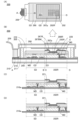
図1は本発明の一態様の機能パネルの構成を説明する図である。図1(A)は本発明の一
態様の機能パネル200の上面図であり、図1(B)は図1(A)の切断線A-Bおよび
切断線C-Dにおける断面図である。また、図1(C)および図1(D)は、図1(B)
に示す一部の構成を置き換えることができる構成を説明する断面図である。
1A is a diagram illustrating a structure of a functional panel according to one embodiment of the present invention. FIG. 1A is a top view of a
13 is a cross-sectional view illustrating a configuration that can replace a portion of the configuration shown in FIG.
<機能パネルの構成例1.>
本実施の形態で説明する機能パネル200は、第1の基材210と、第1の基材210と
重なる領域を備える第2の基材270と、第1の基材210の一方の面に第2の基材27
0を接合する機能を備える接合層205と、第1の基材210、第2の基材270および
接合層205に接する絶縁層290と、第1の基材210、第2の基材270および接合
層205に囲まれた領域に機能層と、を有する(図1(A)参照)。
<Function panel configuration example 1.>
The
1A, the insulating
そして、機能層は、複数の機能素子を備える。 The functional layer then has multiple functional elements.
本実施の形態で説明する機能パネル200は、第1の基材210と、第2の基材270と
、第1の基材210および第2の基材270を接合する接合層205と、第1の基材21
0、第2の基材270および接合層205と、に接する絶縁層290を含んで構成される
。また、可撓性を備える材料を第1の基材210および第2の基材270に用いることが
できる。
The
The
これにより、接合層が第1の基材に接する領域または接合層が第2の基材に接する領域に
生じ易い隙間を、絶縁層により埋めることができ、第1の基材と、第2の基材と、第1の
基材および第2の基材を接合する接合層に囲まれた領域にある機能層に、不純物が拡散す
る現象を抑制することができる。また、可撓性を備える材料を第1の基材210および第
2の基材270に用いると、折り曲げることまたは折り畳むことができる。その結果、利
便性または信頼性に優れた新規な機能パネルを提供できる。
This allows the insulating layer to fill gaps that tend to occur in the area where the bonding layer contacts the first substrate or the area where the bonding layer contacts the second substrate, and suppresses the phenomenon of impurities diffusing into the functional layer in the area surrounded by the first substrate, the second substrate, and the bonding layer that bonds the first substrate and the second substrate. In addition, when a flexible material is used for the
なお、発光素子250Rを機能素子に用いることができる。また、発光素子250Rを備
える機能パネル200は発光モジュールということができる。
The
また、表示素子を機能素子に用いることができる。また、表示素子を備える機能パネル2
00は表示モジュールということができる。
In addition, a display element can be used as a functional element.
00 can be said to be a display module.
また、駆動トランジスタM0を機能素子に用いることができる。 In addition, the drive transistor M0 can be used as a functional element.
また、本発明の一態様の機能パネル200は、画素202、画素202に制御信号を供給
する駆動回路GD、画素202に表示信号を供給する駆動回路SDおよび画素202が配
設される領域201を有する(図1(A)および図1(B)参照)。
A
画素202は、表示信号を供給される(図1(A)参照)。画素202は、副画素202
R等を備える。副画素202Rは赤色の表示をする機能を備える。また、例えば、緑色の
表示をする副画素および青色の表示をする副画素等を備える。
A display signal is supplied to the pixel 202 (see FIG. 1A).
The sub-pixel 202R has a function of displaying red. In addition, for example, a sub-pixel that displays green and a sub-pixel that displays blue are also provided.
副画素202Rは、画素回路および表示モジュール280Rを備える(図1(B)参照)
。
The
.
画素回路は、駆動トランジスタM0および容量素子Cを含む。 The pixel circuit includes a drive transistor M0 and a capacitance element C.
表示モジュール280Rは、発光素子250R、発光素子250Rが光を射出する側に発
光素子250Rと重なる領域を有する着色層267Rを備える。なお、発光素子250R
は表示素子の一態様であるということができる。
The
It can be said that the above is one aspect of a display element.
発光素子250Rは、下部電極、上部電極、発光性の有機化合物を含む層を備える。
The light-emitting
回路は駆動トランジスタM0を備え且つ第1の基材210および発光素子250Rの間に
配設される。また、回路は絶縁膜221を発光素子250Rとの間に挟む。
The circuit includes a driving transistor M0 and is disposed between the
駆動トランジスタM0は第2の電極を備える。第2の電極は、絶縁膜221に設けられた
開口部を介して発光素子250Rの下部電極と電気的に接続される。
The driving transistor M0 has a second electrode. The second electrode is electrically connected to the lower electrode of the
容量素子Cは、第1の電極と第2の電極を備える。第1の電極は、駆動トランジスタM0
のゲートに電気的に接続され、第2の電極は、駆動トランジスタM0の第2の電極と電気
的に接続される。
The capacitance element C has a first electrode and a second electrode. The first electrode is connected to the driving transistor M0
and a second electrode electrically connected to the second electrode of the driving transistor M0.
駆動回路SDは、トランジスタMDおよび容量CDを備える。 The drive circuit SD includes a transistor MD and a capacitance CD.
本発明の一態様の機能パネル200は、駆動回路SDと電気的に接続される配線211と
、配線211と電気的に接続される端子219と、端子219と電気的に接続されるフレ
キシブルプリント基板209と、を有する。
A
また、副画素202Rと重なる領域に開口部を備える遮光層267BMを備える。
It also has a light-shielding layer 267BM with an opening in the area overlapping with the
また、発光素子250Rと重なる領域に開口部を備え、下部電極の端部を覆う隔壁228
を備える。
In addition, a
Equipped with.
また、領域201に重なる領域を備える機能膜267pを有する(図1(B)参照)。
It also has a
なお、機能パネル200は第2の基材270が設けられている側に表示情報を表示するこ
とができる。
The
以下に、本発明の一態様の機能パネル200を構成する個々の要素について説明する。な
お、これらの構成は明確に分離できず、一つの構成が他の構成を兼ねる場合や他の構成の
一部を含む場合がある。
The individual elements constituting the
《全体の構成》
機能パネル200は、第1の基材210、第2の基材270、接合層205、絶縁層29
0または機能層を有する。
Overall Composition
The
0 or functional layer.
また、機能パネル200は、画素202、駆動回路GD、駆動回路SD、領域201。副
画素202R、駆動トランジスタM0、容量素子C、表示モジュール280R、発光素子
250R、着色層267R、画素回路、絶縁膜221、配線211、端子219、フレキ
シブルプリント基板209、遮光層267BM、隔壁228または機能膜267pを備え
る。
The
《第1の基材210》
第1の基材210は、製造工程に耐えられる程度の耐熱性および製造装置に適用可能な厚
さおよび大きさを備えるものであれば、特に限定されない。
<<
There are no particular limitations on the
有機材料、無機材料または有機材料と無機材料等の複合材料等を第1の基材210に用い
ることができる。例えば、ガラス、セラミックス、金属等の無機材料を第1の基材210
に用いることができる。
An organic material, an inorganic material, or a composite material of an organic material and an inorganic material can be used for the
can be used.
具体的には、無アルカリガラス、ソーダ石灰ガラス、カリガラスまたはクリスタルガラス
等を、第1の基材210に用いることができる。具体的には、無機酸化物膜、無機窒化物
膜または無機酸窒化物膜等を、第1の基材210に用いることができる。例えば、酸化珪
素、窒化珪素、酸窒化珪素、アルミナ膜等を、第1の基材210に用いることができる。
SUSまたはアルミニウム等を、第1の基材210に用いることができる。
Specifically, alkali-free glass, soda-lime glass, potash glass, crystal glass, or the like can be used for the
The
例えば、樹脂、樹脂フィルムまたはプラスチック等の有機材料を第1の基材210に用い
ることができる。具体的には、ポリエステル、ポリオレフィン、ポリアミド、ポリイミド
、ポリカーボネートまたはアクリル樹脂等の樹脂フィルムまたは樹脂板を、第1の基材2
10に用いることができる。
For example, a resin, a resin film, or an organic material such as plastic can be used for the
10 can be used.
例えば、金属板、薄板状のガラス板または無機材料等の膜を樹脂フィルム等に貼り合わせ
た複合材料を第1の基材210に用いることができる。例えば、繊維状または粒子状の金
属、ガラスもしくは無機材料等を樹脂フィルムに分散した複合材料を、第1の基材210
に用いることができる。例えば、繊維状または粒子状の樹脂もしくは有機材料等を無機材
料に分散した複合材料を、第1の基材210に用いることができる。
For example, a composite material in which a metal plate, a thin glass plate, or a film of an inorganic material is bonded to a resin film or the like can be used for the
For example, the
また、単層の材料または複数の層が積層された材料を、第1の基材210に用いることが
できる。例えば、基材と基材に含まれる不純物の拡散を防ぐ絶縁膜等が積層された材料を
、第1の基材210に用いることができる。具体的には、ガラスとガラスに含まれる不純
物の拡散を防ぐ酸化シリコン層、窒化シリコン層または酸化窒化シリコン層等から選ばれ
た一または複数の膜が積層された材料を、第1の基材210に適用できる。または、樹脂
と樹脂を透過する不純物の拡散を防ぐ酸化シリコン膜、窒化シリコン膜または酸化窒化シ
リコン膜等が積層された材料を、第1の基材210に適用できる。
Also, a single-layer material or a material having multiple layers laminated thereon can be used for the
また、可撓性を有する材料を第1の基材210に用いることができる。例えば、折り曲げ
ることができる程度または折り畳むことができる程度の可撓性を有する材料を用いること
ができる。具体的には5mm以上、好ましくは4mm以上、より好ましくは3mm以上、
特に好ましくは1mm以上の曲率半径で屈曲できる材料を用いることができる。また、厚
さが2.5μm以上3mm以下好ましくは5μm以上1.5mm以下より好ましくは10
μm以上500μm以下の材料を第1の基材210に用いることができる(図2参照)。
A flexible material can be used for the
Particularly preferably, a material that can be bent with a radius of curvature of 1 mm or more can be used.
A material having a thickness of 500 μm or more can be used for the first base material 210 (see FIG. 2).
具体的には、可撓性を有する基材210b、不純物の拡散を防ぐバリア膜210aおよび
基材210bとバリア膜210aを貼り合わせる樹脂層210cが積層された積層体を第
1の基材210に用いることができる。
Specifically, the
《第2の基材270》
第1の基材210に用いることができ且つ表示素子と重なる領域に透光性を有する材料を
、第2の基材270に用いることができる。また、可撓性を有する材料を第2の基材27
0に用いることができる。具体的には、可撓性を有する基材270b、不純物の拡散を防
ぐバリア膜270aおよび基材270bとバリア膜270aを貼り合わせる樹脂層270
cが積層された積層体を第2の基材270に用いることができる。
<<
A material that can be used for the
Specifically, the
A laminate in which c is laminated can be used as the
《接合層205》
第1の基材210および第2の基材270を貼り合わせることができる材料を、接合層2
05に用いることができる。
<<
A material capable of bonding the
It can be used for 05.
無機材料、有機材料または無機材料と有機材料の複合材料等を接合層205に用いること
ができる。
The
例えば、融点が400℃以下好ましくは300℃以下のガラス層または接着剤等を用いる
ことができる。
For example, a glass layer or adhesive having a melting point of 400° C. or less, preferably 300° C. or less, can be used.
例えば、光硬化型接着剤、反応硬化型接着剤、熱硬化型接着剤または/および嫌気型接着
剤等の有機材料を接合層205に用いることができる。
For example, organic materials such as a photocurable adhesive, a reaction curable adhesive, a heat curable adhesive, and/or an anaerobic adhesive can be used for the
具体的には、エポキシ樹脂、アクリル樹脂、シリコーン樹脂、フェノール樹脂、ポリイミ
ド樹脂、イミド樹脂、PVC(ポリビニルクロライド)樹脂、PVB(ポリビニルブチラ
ル)樹脂、EVA(エチレンビニルアセテート)樹脂等を含む接着剤を用いることができ
る。
Specifically, adhesives containing epoxy resin, acrylic resin, silicone resin, phenol resin, polyimide resin, imide resin, PVC (polyvinyl chloride) resin, PVB (polyvinyl butyral) resin, EVA (ethylene vinyl acetate) resin, etc. can be used.
《絶縁層290》
電気的な絶縁性を備える材料または不純物の拡散を抑制する機能を備える材料を絶縁層2
90に用いることができる。例えば、酸化物、窒化物、フッ化物、硫化物、三元化合物、
金属またはポリマーを絶縁層290に用いることができる。
<Insulating
A material having electrical insulation properties or a material having a function of suppressing the diffusion of impurities is used as the insulating
90. For example, oxides, nitrides, fluorides, sulfides, ternary compounds,
Metals or polymers can be used for the insulating
例えば、酸化アルミニウム、酸化ハフニウム、ハフニウムシリケート、酸化ランタン、酸
化珪素、チタン酸ストロンチウム、酸化タンタル、酸化チタン、酸化亜鉛、酸化ニオブ、
酸化ジルコニウム、酸化スズ、酸化イットリウム、酸化セリウム、酸化スカンジウム、酸
化エルビウム、酸化バナジウムまたは酸化インジウム等を含む材料を用いることができる
。
For example, aluminum oxide, hafnium oxide, hafnium silicate, lanthanum oxide, silicon oxide, strontium titanate, tantalum oxide, titanium oxide, zinc oxide, niobium oxide,
Materials including zirconium oxide, tin oxide, yttrium oxide, cerium oxide, scandium oxide, erbium oxide, vanadium oxide, indium oxide, or the like can be used.
例えば、窒化アルミニウム、窒化ハフニウム、窒化珪素、窒化タンタル、窒化チタン、窒
化ニオブ、窒化モリブデン、窒化ジルコニウムまたは窒化ガリウム等を含む材料を用いる
ことができる。
For example, materials including aluminum nitride, hafnium nitride, silicon nitride, tantalum nitride, titanium nitride, niobium nitride, molybdenum nitride, zirconium nitride, gallium nitride, and the like can be used.
例えば、銅、白金、ルテニウム、タングステン、イリジウム、パラジウム、鉄、コバルト
またはニッケル等を含む材料を用いることができる。
For example, materials containing copper, platinum, ruthenium, tungsten, iridium, palladium, iron, cobalt, nickel, or the like can be used.
例えば、硫化亜鉛、硫化ストロンチウム、硫化カルシウム、硫化鉛、フッ化カルシウム、
フッ化ストロンチウムまたはフッ化亜鉛等を含む材料を用いることができる。
For example, zinc sulfide, strontium sulfide, calcium sulfide, lead sulfide, calcium fluoride,
Materials including strontium fluoride or zinc fluoride, etc., can be used.
例えば、チタンおよびアルミニウムを含む窒化物、チタンおよびアルミニウムを含む酸化
物、アルミニウムおよび亜鉛を含む酸化物、マンガンおよび亜鉛を含む硫化物、セリウム
およびストロンチウムを含む硫化物、エルビウムおよびアルミニウムを含む酸化物、イッ
トリウムおよびジルコニウムを含む酸化物等を含む材料を用いることができる。
For example, materials including nitrides containing titanium and aluminum, oxides containing titanium and aluminum, oxides containing aluminum and zinc, sulfides containing manganese and zinc, sulfides containing cerium and strontium, oxides containing erbium and aluminum, oxides containing yttrium and zirconium, etc. can be used.
例えば、原子層堆積(ALD:Atomic Layer Deposition)法を
用いて形成することができる材料を、絶縁層290に用いることができる。緻密な、クラ
ックやピンホールなどの欠陥が低減された、または均一な厚さを備える絶縁層290を、
原子層堆積法を用いて形成することができる。また、絶縁層290を形成する際に加工部
材に与える損傷を、低減することができる。
For example, a material that can be formed by using an atomic layer deposition (ALD) method can be used for the insulating
The insulating
《機能層》
機能回路、機能素子、光学素子または機能膜等もしくはこれらから選ばれた複数を含む層
を、機能層に用いることができる。
<Functional Layer>
A functional circuit, a functional element, an optical element, or a functional film, or a layer including a plurality of elements selected from these, can be used as the functional layer.
例えば、電気素子またはバイオチップ等を機能層に用いることができる。具体的には、ト
ランジスタ、容量素子、抵抗素子、記憶素子、発光素子または表示素子等を用いることが
できる。
For example, an electric element, a biochip, or the like can be used for the functional layer. Specifically, a transistor, a capacitor, a resistor, a memory element, a light-emitting element, a display element, or the like can be used.
例えば、表示素子と表示素子を駆動する画素回路を機能層に用いることができる。 For example, a display element and a pixel circuit that drives the display element can be used as the functional layer.
例えば、タッチセンサ、カラーフィルタまたは防湿膜等を機能層に用いることができる。 For example, a touch sensor, a color filter, or a moisture-proof film can be used as a functional layer.
《領域201》
領域201は、複数の機能素子を備える。例えば、マトリクス状に配設された機能素子を
備える。具体的には、マトリクス状に配設された複数の画素202を備える。これにより
、機能パネル200は画像情報を領域201に表示できる。
"
The
《画素202》
複数の副画素を画素202に用いることができる。例えば、赤色を表示する副画素202
Rと、緑色を表示する副画素と、青色を表示する副画素と、を用いることができる。また
、黄色を表示する副画素、白色を表示する副画素、シアンを表示する副画素、マゼンタを
表示する副画素等を用いることができる。
<<
Multiple sub-pixels can be used in the
A sub-pixel that displays R, a sub-pixel that displays green, and a sub-pixel that displays blue can be used. In addition, a sub-pixel that displays yellow, a sub-pixel that displays white, a sub-pixel that displays cyan, a sub-pixel that displays magenta, etc. can be used.
《副画素》
表示素子および表示素子を駆動する画素回路を副画素に用いることができる。
<<Subpixel>>
A display element and a pixel circuit for driving the display element can be used for the sub-pixel.
また、絶縁膜221を、表示素子を含む機能層と画素回路を含む機能層の間に用いること
ができる。
In addition, the insulating
例えば、無機材料、有機材料または無機材料と有機材料の複合材料を絶縁膜221に用い
ることができる。具体的には、珪素および窒素を含む膜、珪素および酸素を含む膜、ポリ
イミドを含む膜、アクリル樹脂を含む膜、シリコーン樹脂を含む膜またはこれらの膜から
選ばれた複数の膜が積層された膜などを、絶縁膜221に用いることができる。
For example, an inorganic material, an organic material, or a composite material of an inorganic material and an organic material can be used for the insulating
なお、機能パネル200は、副画素202Rと重なる領域に開口部を備える遮光層267
BMを備える。遮光層267BMは、遮光性を有する。
The
The light-shielding layer 267BM has a light-shielding property.
例えば、顔料を分散した樹脂、染料を含む樹脂の他、黒色クロム膜等の無機膜を遮光層2
67BMに用いることができる。具体的には、カーボンブラック、無機酸化物、複数の無
機酸化物の固溶体を含む複合酸化物等を遮光層267BMに用いることができる。
For example, a resin containing a pigment dispersed therein, a resin containing a dye, or an inorganic film such as a black chrome film may be used as the light-
Specifically, carbon black, an inorganic oxide, a composite oxide including a solid solution of a plurality of inorganic oxides, or the like can be used for the light-shielding layer 267BM.
なお、表示素子と重なる領域に開口部を備える隔壁228を機能パネル200に用いるこ
とができる。例えば、隔壁228が重ねて設けられた導電膜の、隔壁228の開口部に重
なる領域を、発光素子250Rの下部電極に用いることができる。これにより、段差が下
部電極の端部に生じないようにすることができる。
Note that the
《表示素子》
例えば、電気的または磁気的作用により、コントラスト、輝度、反射率、透過率などが変
化する表示媒体を表示素子に用いることができる。
Display element
For example, a display medium whose contrast, brightness, reflectance, transmittance, etc. change due to electrical or magnetic effects can be used as a display element.
なお、発光素子250Rと、発光素子250Rが射出する光の少なくとも一部を透過する
着色層267Rと、を備える表示モジュール280Rを表示素子に用いることができる。
Note that a
例えば、顔料または染料等の材料を含む層を着色層267Rに用いることができる。これ
により、表示モジュール280Rが射出する光の色と特定の色にすることができる。
For example, a layer containing a material such as a pigment or dye can be used for the
また、反射膜と、半透過・半反射膜の間に発光素子250Rが配置された微小共振器構造
を用いることができる。具体的には、反射性の導電膜を一方の電極に、半透過・半反射性
の導電膜を他方の電極に備える発光素子250Rを用いることができる。
Also, a microresonator structure in which the
例えば、赤色の光を効率よく取り出す微小共振器および赤色の光を透過する着色層を、赤
色を表示する表示モジュール280Rに用い、緑色の光を効率よく取り出す微小共振器お
よび緑色の光を透過する着色層を、緑色を表示する表示モジュールに用い、または青色の
光を効率よく取り出す微小共振器および青色の光を透過する着色層を、青色を表示する表
示モジュールに用いてもよい。
For example, a microresonator that efficiently extracts red light and a colored layer that transmits red light may be used in a
なお、そして、黄色の光を効率よく取り出す微小共振器および黄色の光を透過する着色層
と共に表示モジュールに用いてもよい。
Furthermore, it may be used in a display module together with a microresonator that efficiently extracts yellow light and a colored layer that transmits yellow light.
具体的には、EL(エレクトロルミネッセンス)素子(有機物及び無機物を含むEL素子
、有機EL素子、無機EL素子)、LED(白色LED、赤色LED、緑色LED、青色
LEDなど)、トランジスタ(電流に応じて発光するトランジスタ)、電子放出素子、液
晶素子、電子インク、電気泳動素子、グレーティングライトバルブ(GLV)、プラズマ
ディスプレイ(PDP)、MEMS(マイクロ・エレクトロ・メカニカル・システム)を
用いた表示素子、デジタルマイクロミラーデバイス(DMD)、DMS(デジタル・マイ
クロ・シャッター)、MIRASOL(登録商標)、IMOD(インターフェアレンス・
モジュレーション)素子、シャッター方式のMEMS表示素子、光干渉方式のMEMS表
示素子、エレクトロウェッティング素子、圧電セラミックディスプレイ、カーボンナノチ
ューブを用いた表示素子、などを用いることができる。
Specifically, EL (electroluminescence) elements (EL elements containing organic and inorganic materials, organic EL elements, inorganic EL elements), LEDs (white LEDs, red LEDs, green LEDs, blue LEDs, etc.), transistors (transistors that emit light in response to electric current), electron emission elements, liquid crystal elements, electronic ink, electrophoretic elements, grating light valves (GLV), plasma displays (PDPs), display elements using MEMS (micro-electro-mechanical systems), digital micromirror devices (DMDs), DMS (digital micro shutters), MIRASOL (registered trademark), IMOD (interference modulus),
It is possible to use a display element using a modulation element, a shutter type MEMS display element, an optical interference type MEMS display element, an electrowetting element, a piezoelectric ceramic display, a display element using carbon nanotubes, and the like.
《画素回路》
表示素子に適したさまざまな画素回路を用いることができる。
《Pixel circuit》
Various pixel circuits suitable for the display element can be used.
例えば、駆動トランジスタM0または容量素子Cを備える画素回路を用いることができる
。
For example, a pixel circuit including a driving transistor M0 or a capacitive element C can be used.
さまざまなトランジスタを駆動トランジスタM0に用いることができる。 A variety of transistors can be used for the drive transistor M0.
例えば、半導体層に14族の元素、化合物半導体または酸化物半導体などを用いるトラン
ジスタを適用できる。具体的には、シリコンを含む半導体、ガリウムヒ素を含む半導体ま
たはインジウムを含む酸化物半導体などを用いるトランジスタを駆動トランジスタM0の
半導体層に適用できる。
For example, a transistor using a Group 14 element, a compound semiconductor, an oxide semiconductor, or the like in a semiconductor layer can be used. Specifically, a transistor using a semiconductor containing silicon, a semiconductor containing gallium arsenide, an oxide semiconductor containing indium, or the like can be used in the semiconductor layer of the driving transistor M0.
例えば、単結晶シリコン、ポリシリコンまたはアモルファスシリコンなどを駆動トランジ
スタM0の半導体層に適用できる。
For example, single crystal silicon, polysilicon, or amorphous silicon can be used for the semiconductor layer of the drive transistor M0.
例えば、ボトムゲート型のトランジスタ、トップゲート型のトランジスタ等を適用できる
。
For example, a bottom-gate transistor, a top-gate transistor, or the like can be used.
《駆動回路》
シフトレジスタ等の様々な順序回路等を、駆動回路GDまたは駆動回路SDに用いること
ができる。
<Drive circuit>
Various sequential circuits such as a shift register can be used for the driver circuit GD or the driver circuit SD.
また、さまざまなトランジスタを駆動回路SDのトランジスタMDに用いることができる
。例えば、駆動トランジスタM0と同一の工程で形成することができる構成を、トランジ
スタMDに用いることができる。
In addition, various transistors can be used for the transistor MD of the driver circuit SD. For example, a structure that can be formed in the same process as the driver transistor M0 can be used for the transistor MD.
また、容量素子Cと同一の構成を容量素子CDに用いることができる。 In addition, the same configuration as that of the capacitance element C can be used for the capacitance element CD.
《配線、端子》
導電性を有する材料を配線211または端子219に用いることができる。
<Wiring, terminals>
A conductive material can be used for the
例えば、無機導電性材料、有機導電性材料、金属または導電性セラミックスなどを配線2
11または端子219に用いることができる。
For example, inorganic conductive materials, organic conductive materials, metals, conductive ceramics, etc. are used for the
11 or
具体的には、アルミニウム、金、白金、銀、クロム、タンタル、チタン、モリブデン、タ
ングステン、ニッケル、鉄、コバルト、パラジウムまたはマンガンから選ばれた金属元素
、上述した金属元素を含む合金または上述した金属元素を組み合わせた合金などを配線2
11または端子219に用いることができる。
Specifically, a metal element selected from aluminum, gold, platinum, silver, chromium, tantalum, titanium, molybdenum, tungsten, nickel, iron, cobalt, palladium, and manganese, an alloy containing the above-mentioned metal element, or an alloy combining the above-mentioned metal elements, etc., may be used as the
11 or
酸化インジウム、インジウム錫酸化物、インジウム亜鉛酸化物、酸化亜鉛、ガリウムを添
加した酸化亜鉛などの導電性酸化物を配線211または端子219に用いることができる
。
A conductive oxide such as indium oxide, indium tin oxide, indium zinc oxide, zinc oxide, or zinc oxide doped with gallium can be used for the
グラフェンまたはグラファイトを導電膜に用いることができる。グラフェンを含む膜は、
例えば膜状に形成された酸化グラフェンを含む膜を還元して形成することができる。還元
する方法としては、熱を加える方法や還元剤を用いる方法等を挙げることができる。
Graphene or graphite can be used for the conductive film. The film containing graphene is
For example, the graphene oxide film can be reduced by applying heat or using a reducing agent.
導電性高分子を用いることができる。 Conductive polymers can be used.
なお、端子219をフレキシブルプリント基板209と電気的に接続することができる。
例えば、異方性導電膜を用いて電気的に接続できる。
The terminal 219 can be electrically connected to the flexible printed
For example, electrical connection can be achieved using an anisotropic conductive film.
《その他》
機能パネル200は機能膜267pを有する。
"others"
The
例えば、無機材料、有機材料または無機材料と有機材料の複合材料などを含む膜を機能膜
267pに用いることができる。具体的には、アルミナまたは酸化珪素などを含むセラミ
ックコート層、UV硬化樹脂等のハードコート層、反射防止膜、円偏光板などを機能膜2
67pに用いることができる。
For example, a film containing an inorganic material, an organic material, or a composite material of an inorganic material and an organic material can be used for the
It can be used for 67p.
《トランジスタ》
さまざまなトランジスタを駆動トランジスタM0またはトランジスタMDに用いることが
できる。
"Transistor"
A variety of transistors can be used for drive transistor M0 or transistor MD.
例えば、ボトムゲート型のトランジスタを駆動トランジスタM0またはトランジスタMD
に用いることができる。
For example, a bottom gate type transistor may be a driving transistor M0 or a transistor MD
can be used.
例えば、酸化物半導体、アモルファスシリコン等を含む半導体層を、駆動トランジスタM
0およびトランジスタMDに適用することができる。
For example, a semiconductor layer including an oxide semiconductor, amorphous silicon, etc. is used as the driving transistor M
0 and transistor MD.
例えば、少なくともインジウム(In)、亜鉛(Zn)及びM(Al、Ga、Ge、Y、
Zr、Sn、La、CeまたはHf等の金属)を含むIn-M-Zn酸化物で表記される
膜を含むことが好ましい。または、InとZnの双方を含むことが好ましい。
For example, at least indium (In), zinc (Zn) and M (Al, Ga, Ge, Y,
Preferably, the oxide film contains a film represented by In-M-Zn oxide, which contains an element selected from the group consisting of In, Sn, La, Ce, and Hf, or a metal such as In. Alternatively, the oxide film contains both In and Zn.
スタビライザーとしては、ガリウム(Ga)、スズ(Sn)、ハフニウム(Hf)、アル
ミニウム(Al)、またはジルコニウム(Zr)等がある。また、他のスタビライザーと
しては、ランタノイドである、ランタン(La)、セリウム(Ce)、プラセオジム(P
r)、ネオジム(Nd)、サマリウム(Sm)、ユウロピウム(Eu)、ガドリニウム(
Gd)、テルビウム(Tb)、ジスプロシウム(Dy)、ホルミウム(Ho)、エルビウ
ム(Er)、ツリウム(Tm)、イッテルビウム(Yb)、ルテチウム(Lu)等がある
。
The stabilizer may be gallium (Ga), tin (Sn), hafnium (Hf), aluminum (Al), or zirconium (Zr). Other stabilizers include lanthanides such as lanthanum (La), cerium (Ce), and praseodymium (P).
r), neodymium (Nd), samarium (Sm), europium (Eu), gadolinium (
Examples of such elements include arsenic (Au), terbium (Tb), dysprosium (Dy), holmium (Ho), erbium (Er), thulium (Tm), ytterbium (Yb), and lutetium (Lu).
酸化物半導体膜を構成する酸化物半導体として、例えば、In-Ga-Zn系酸化物、I
n-Al-Zn系酸化物、In-Sn-Zn系酸化物、In-Hf-Zn系酸化物、In
-La-Zn系酸化物、In-Ce-Zn系酸化物、In-Pr-Zn系酸化物、In-
Nd-Zn系酸化物、In-Sm-Zn系酸化物、In-Eu-Zn系酸化物、In-G
d-Zn系酸化物、In-Tb-Zn系酸化物、In-Dy-Zn系酸化物、In-Ho
-Zn系酸化物、In-Er-Zn系酸化物、In-Tm-Zn系酸化物、In-Yb-
Zn系酸化物、In-Lu-Zn系酸化物、In-Sn-Ga-Zn系酸化物、In-H
f-Ga-Zn系酸化物、In-Al-Ga-Zn系酸化物、In-Sn-Al-Zn系
酸化物、In-Sn-Hf-Zn系酸化物、In-Hf-Al-Zn系酸化物、In-G
a系酸化物を用いることができる。
Examples of oxide semiconductors that form the oxide semiconductor film include In—Ga—Zn-based oxides, I
n-Al-Zn oxide, In-Sn-Zn oxide, In-Hf-Zn oxide, In
-La-Zn oxide, In-Ce-Zn oxide, In-Pr-Zn oxide, In-
Nd-Zn oxide, In-Sm-Zn oxide, In-Eu-Zn oxide, In-G
d-Zn oxide, In-Tb-Zn oxide, In-Dy-Zn oxide, In-Ho
-Zn-based oxides, In-Er-Zn-based oxides, In-Tm-Zn-based oxides, In-Yb-
Zn-based oxides, In-Lu-Zn-based oxides, In-Sn-Ga-Zn-based oxides, In-H
f-Ga-Zn oxide, In-Al-Ga-Zn oxide, In-Sn-Al-Zn oxide, In-Sn-Hf-Zn oxide, In-Hf-Al-Zn oxide, In-G
A-series oxides can be used.
なお、ここで、In-Ga-Zn系酸化物とは、InとGaとZnを主成分として有する
酸化物という意味であり、InとGaとZnの比率は問わない。また、InとGaとZn
以外の金属元素が入っていてもよい。
In this case, the In-Ga-Zn oxide means an oxide having In, Ga, and Zn as main components, and the ratio of In, Ga, and Zn does not matter.
Metal elements other than those may be included.
例えば、レーザーアニールなどの処理により結晶化させた多結晶シリコンを含む半導体層
を駆動トランジスタM0およびトランジスタMDに適用できる(図1(C)参照)。
For example, a semiconductor layer including polycrystalline silicon crystallized by a process such as laser annealing can be used for the driving transistor M0 and the transistor MD (see FIG. 1C).
例えば、トップゲート型のトランジスタを駆動トランジスタM0およびトランジスタMD
に適用できる(図1(D)参照)。
For example, the top-gate type transistors are the driving transistor M0 and the transistor MD
(See FIG. 1(D)).
例えば、多結晶シリコンを含む半導体層または単結晶シリコン基板等から転置された単結
晶シリコン膜等を含む半導体層を駆動トランジスタM0およびトランジスタMDに適用す
ることができる。
For example, a semiconductor layer including polycrystalline silicon or a semiconductor layer including a single crystal silicon film transferred from a single crystal silicon substrate or the like can be applied to the driving transistor M0 and the transistor MD.
本発明の一態様の機能パネルの別の構成について、図17乃至図22を参照しながら説明
する。
Another configuration of the functional panel according to an embodiment of the present invention will be described with reference to FIGS.
図17乃至図22は本発明の一態様の機能パネルの構成を説明する図である。図17(A
)乃至図22(A)は本発明の一態様の機能パネルの上面図であり、図17(B)乃至図
22(B)はそれぞれ対応する図17(A)乃至図22(A)の切断線A-Bおよび切断
線C-Dにおける断面図である。図17(C)乃至図22(C)および図17(D)乃至
図22(D)は、それぞれ対応する図17(B)乃至図22(B)に示す一部の構成を置
き換えることができる構成を説明する断面図である。
17 to 22 are diagrams illustrating a configuration of a functional panel according to one embodiment of the present invention.
17(B) to 22(B) are cross-sectional views taken along the cutting lines A-B and C-D in the corresponding Figs. 17(A) to 22(A), respectively. Figs. 17(C) to 22(C) and Figs. 17(D) to 22(D) are cross-sectional views illustrating configurations that can replace some of the configurations shown in the corresponding Figs. 17(B) to 22(B), respectively.
機能パネル200(1)は絶縁層291を有し、絶縁層291と第1の基材210との間
に発光素子250Rを備える点が、機能パネル200と異なる(図17(B)および図1
8(B)参照)。
The functional panel 200(1) differs from the
See 8(B)).
絶縁層290に用いることができる材料を絶縁層291に用いることができる。また、絶
縁層290と同様の方法を用いて絶縁層291を形成できる。
The insulating
機能パネル200(2)は絶縁層291を有し、絶縁層291と第1の基材210との間
に駆動トランジスタM0を備える点が、機能パネル200と異なる(図19および図20
参照)。
The functional panel 200(2) differs from the
reference).
絶縁層290に用いることができる材料を絶縁層291に用いることができる。また、絶
縁層290と同様の方法を用いて絶縁層291を形成できる。
The insulating
機能パネル200(3)は絶縁層290と第2の基材270との間に機能膜267pを備
える点が、機能パネル200と異なる(図21および図22参照)。
Functional panel 200(3) differs from
<機能パネルの構成例2.>
本発明の一態様の機能パネルの別の構成について、図3を参照しながら説明する。
<Function panel configuration example 2.>
Another configuration of the functional panel according to an embodiment of the present invention will be described with reference to FIG.
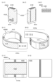
図3は本発明の一態様の機能パネルの構成を説明する図である。図3(A)は本発明の一
態様の機能パネル200Bの上面図であり、図3(B)は図3(A)の切断線A-Bおよ
び切断線C-Dにおける断面図である。図3(C)および図3(D)は、図3(B)に示
す一部の構成を置き換えることができる構成を説明する断面図である。
3A and 3B are diagrams illustrating a configuration of a functional panel according to one embodiment of the present invention. Fig. 3A is a top view of a
本実施の形態で説明する機能パネル200Bは、副画素202Rと重なる領域に開口部を
備える遮光層267BMおよび着色層267Rが第1の基材210と発光素子250Rの
間に配置されている点、機能膜267pが第1の基材210側に設けられている点および
表示モジュール280Rが光を第1の基材210が設けられている側に射出する点が、図
1を参照しながら説明する機能パネル200と異なる。
The
第1の基材210は、透光性を表示素子と重なる領域に備え、第2の基材270は、必ず
しも透光性を備える必要はない。他の構成は同様の構成を用いることができる。
The
これにより、機能パネル200Bは第1の基材210が設けられている側に表示情報を表
示することができる。
This allows the
また、可撓性を有する材料を第1の基材210および第2の基材270に用いることがで
きる。例えば、折り曲げることができる程度または折り畳むことができる程度の可撓性を
有する材料を用いることができる。具体的には、可撓性を有する基材210b、不純物の
拡散を防ぐバリア膜210aおよび基材210bとバリア膜210aを貼り合わせる樹脂
層210cが積層された積層体を、第1の基材210に用いることができる。また、可撓
性を有する基材270b、不純物の拡散を防ぐバリア膜270aおよび基材270bとバ
リア膜270aを貼り合わせる樹脂層270cが積層された積層体を、第2の基材270
に用いることができる(図4参照)。
Moreover, a flexible material can be used for the
(See FIG. 4).
なお、本実施の形態は、本明細書で示す他の実施の形態と適宜組み合わせることができる
。
Note that this embodiment mode can be appropriately combined with other embodiment modes described in this specification.
(実施の形態2)
本実施の形態では、本発明の一態様の機能パネルの作製方法について、図5乃至図8を参
照しながら説明する。
(Embodiment 2)
In this embodiment, a manufacturing method of a functional panel according to one embodiment of the present invention will be described with reference to FIGS.
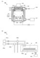
図5は本発明の一態様の機能パネルの作製方法を説明するフロー図であり、図6は工程中
の加工部材の構成を説明する模式図である。図6(A-1)は本発明の一態様の加工部材
の上面模式図であり、図6(B-1)は本発明の一態様の加工部材及び該加工部材を用い
た機能パネルの上面模式図であり、図6(A-2)および図6(B-2)はそれぞれ左側
に示す図の切断線W1-W2における断面模式図である。
Fig. 5 is a flow diagram illustrating a method for manufacturing a functional panel according to one embodiment of the present invention, and Fig. 6 is a schematic diagram illustrating the configuration of a processed member during the process. Fig. 6(A-1) is a schematic top view of a processed member according to one embodiment of the present invention, Fig. 6(B-1) is a schematic top view of a processed member according to one embodiment of the present invention and a functional panel using the processed member, and Fig. 6(A-2) and Fig. 6(B-2) are schematic cross-sectional views taken along the cutting line W1-W2 in the diagram shown on the left side.
<機能パネルの作製方法例1.>
本実施の形態で説明する機能パネルの作製方法は、以下の6つのステップを有する(図5
参照)。
<Example 1 of how to make a functional panel>
The method for manufacturing a functional panel described in this embodiment has the following six steps (FIG. 5
reference).
《第1のステップ》
第1のステップにおいて、加工部材10を準備し、加工部材10を図示されていない加工
部材支持部に供給する(図5(S1)参照)。なお、加工部材支持部は加工部材10の温
度を制御する機能を有する。
First Step
In the first step, the processed
なお、加工部材10は、第1の基材310と、第1の基材310と重なる領域を備える第
2の基材370と、第1の基材310の一方の面に第2の基材370を接合する機能を備
える接合層305と、第1の基材310、第2の基材370および接合層305に囲まれ
た領域に機能層330と、を有する。そして、機能層330は、複数の機能素子を備える
(、図6(A-1)および図6(A-2)参照)。
The processed
《第2のステップ》
第2のステップにおいて、例えば加工部材支持部を用いて加工部材10の温度を所定の値
に制御して、加工部材10および加工部材支持部を内部に備える図示されていないチャン
バーを排気する(図5(S2)参照)。なお、チャンバーは密閉することができる空間を
有する。
Second Step
In a second step, the temperature of the processed
《第3のステップ》
第3のステップにおいて、前駆体化合物を含む原料ガスをチャンバーに供給し、供給した
のち原料ガスをチャンバーからパージする(図5(S3)参照)。例えば金属アルコキシ
ドまたは有機金属化合物等を前駆体化合物に用いることができる。なお、チャンバーを排
気する方法または不活性ガスを導入しながら排気する方法などを、原料ガスをパージする
方法に用いることができる。
<<Third Step>>
In the third step, a source gas containing a precursor compound is supplied to the chamber, and after the supply, the source gas is purged from the chamber (see FIG. 5 (S3)). For example, a metal alkoxide or an organometallic compound can be used as the precursor compound. Note that a method of evacuating the chamber or a method of evacuating while introducing an inert gas can be used as a method of purging the source gas.
《第4のステップ》
第4のステップにおいて、酸化剤を含む原料ガスをチャンバーに供給し、供給したのち原
料ガスをチャンバーからパージする(図5(S4)参照)。例えば、水蒸気、オゾンなど
を酸化剤に用いることができる。なお、このステップを終えたときに、前駆体化合物の酸
化物を含む絶縁層が加工部材10の表面に形成される。この方法によれば、入り組んだ形
状を有する表面に緻密な膜を形成できる。その結果、ピンホール等の欠陥が少ない絶縁層
を形成できる。
The fourth step:
In the fourth step, a source gas containing an oxidizing agent is supplied to the chamber, and after the supply, the source gas is purged from the chamber (see FIG. 5 (S4)). For example, water vapor, ozone, etc. can be used as the oxidizing agent. When this step is completed, an insulating layer containing an oxide of the precursor compound is formed on the surface of the processed
《第5のステップ》
第5のステップにおいて、第3のステップと第4のステップを含むサイクルの繰り返し回
数が、所定の回数未満である場合は、第3のステップに戻り、所定の回数以上である場合
は、第6のステップに進む(図5(S5)参照)。なお、繰り返しの単位は一つのサイク
ルを含み、一つのサイクルは第3のステップと第4のステップを含む。
The fifth step:
In the fifth step, if the number of repetitions of the cycle including the third and fourth steps is less than a predetermined number, the process returns to the third step, and if the number of repetitions is equal to or greater than the predetermined number, the process proceeds to the sixth step (see FIG. 5 (S5)). Note that a unit of repetition includes one cycle, and one cycle includes the third and fourth steps.
なお、2以上の前駆体化合物を交互に供給する方法を第3のステップに用いることができ
る。例えば、第1の前駆体化合物を含む原料ガスを供給する第1の第3のステップと、第
2の前駆体化合物を含む原料ガスを供給する第2の第3のステップと、を用いることもで
きる。この場合、一つのサイクルは第1の第3のステップ、第2の第3のステップおよび
第4のステップを含む。
In addition, a method of alternately supplying two or more precursor compounds can be used for the third step. For example, a first third step of supplying a source gas containing a first precursor compound and a second third step of supplying a source gas containing a second precursor compound can be used. In this case, one cycle includes a first third step, a second third step, and a fourth step.
《第6のステップ》
第6のステップにおいて、加工部材10をチャンバーから搬出する。ここで、絶縁層39
0の形成を終了する(図5(S6)、図6(B-1)および図6(B-2)参照)。なお
、このステップを終えたときに、前駆体化合物の酸化物を含む絶縁層390が所定の厚さ
で表面に形成された機能パネル300を提供することができる。
The Sixth Step
In the sixth step, the processed
0 is completed (see FIG. 5 (S6), FIG. 6 (B-1) and FIG. 6 (B-2)). When this step is completed, it is possible to provide a
本実施の形態で説明する機能パネルの作製方法は、前駆体化合物を含む原料ガスを供給し
、供給したのち原料ガスをチャンバーからパージするステップと、酸化剤を含む原料ガス
を供給し、供給したのち原料ガスをチャンバーからパージするステップと、を含んで構成
される。これにより、加工部材の表面に前駆体化合物の酸化物を含む絶縁層を形成するこ
とができる。その結果、新規な機能パネルの作製方法を提供できる。
The method for producing a functional panel described in this embodiment includes a step of supplying a raw material gas containing a precursor compound, and then purging the raw material gas from a chamber, and a step of supplying a raw material gas containing an oxidizing agent, and then purging the raw material gas from a chamber. This allows an insulating layer containing an oxide of the precursor compound to be formed on the surface of a processed member. As a result, a novel method for producing a functional panel can be provided.
また、本実施の形態で説明する機能パネルの作製方法は、例えば、実施の形態3で説明す
る本発明の一態様の成膜システムを利用して、実施することができる。
The method for manufacturing a functional panel described in this embodiment can be implemented using, for example, the film formation system according to one embodiment of the present invention described in
具体的には、成膜装置100において、第1の基材310に機能層を形成し、封止室SU
において、接合層305を用いて、第1の基材310および第2の基材370を貼り合せ
て第1の基材310を作製することができる。
Specifically, in the
In the above, the
そして、原子層堆積装置ALDを用いて、絶縁層390を形成することができる。
Then, the insulating
また、リフトオフ法等を、加工部材10の一部に絶縁層390を形成しない領域を設ける
方法に用いることができる。
Furthermore, a lift-off method or the like can be used to provide a region in which the insulating
例えば、後の工程で剥離することができるレジストマスクが絶縁層390を形成しない領
域に形成された加工部材を加工部材10に用いる。
For example, a processed member in which a resist mask that can be peeled off in a later step is formed in an area where the insulating
上記の第1のステップから第6のステップまでを実施した後、レジストマスクを剥離する
。これにより、レジストマスク上に形成された絶縁層390を、レジストマスクと共に加
工部材10から分離することができる。
After the above-mentioned first to sixth steps are performed, the resist mask is peeled off, whereby the insulating
具体的には、感光性のレジスト、可溶性の樹脂または粘着テープ等をレジストマスクに用
いることができる。
Specifically, a photosensitive resist, a soluble resin, an adhesive tape, or the like can be used as the resist mask.
<機能パネルの作製方法例2.>
本発明の一態様の機能パネルの作製方法の別の構成について、図7および図8を参照しな
がら説明する。
<Example 2 of how to make a functional panel>
Another method for manufacturing a functional panel according to one embodiment of the present invention will be described with reference to FIGS.
図7は本発明の一態様の機能パネルの作製方法を説明するフロー図であり、図8は工程中
の加工部材の構成を説明する模式図である。図8(A-1)乃至図8(D-1)は本発明
の一態様の加工部材の上面模式図であり、図8(A-2)乃至図8(D-2)はそれぞれ
左側に示す図の切断線W1-W2における断面模式図である。
Fig. 7 is a flow diagram illustrating a method for manufacturing a functional panel according to one embodiment of the present invention, and Fig. 8 is a schematic diagram illustrating a configuration of a processed member during the process. Fig. 8(A-1) to Fig. 8(D-1) are schematic top views of a processed member according to one embodiment of the present invention, and Fig. 8(A-2) to Fig. 8(D-2) are schematic cross-sectional views taken along the cutting line W1-W2 in the diagram shown on the left side.
本実施の形態で説明する機能パネルの作製方法の別の構成は、以下の8つのステップを有
する(図7参照)。なお、例えば、実施の形態3で説明する本発明の一態様の成膜システ
ムを利用して、実施することができる。
Another method for manufacturing a functional panel described in this embodiment includes the following eight steps (see FIG. 7). Note that this method can be implemented by using, for example, the film formation system according to one embodiment of the present invention described in
また、図5を参照しながら説明する機能パネルの作製方法とは、以下の3つの点において
異なる。
Also, this method differs from the method for producing a functional panel described with reference to FIG. 5 in the following three points.
第1の相違点は、加工部材10Bを用いる点である。加工部材10Bは、第1の接合層3
05aと、第2の接合層305bと、第1の基材310、第2の基材370および第1の
接合層305aに囲まれた領域に第1の機能層330aと、第1の基材310、第2の基
材370および第2の接合層305bに囲まれた領域に第2の機能層330bと、を有す
る(図8(A-1)および図8(A-2))。
The first difference is that a processed
05a,
第2の相違点は、第2の基材370の、第1の接合層305aおよび第2の接合層305
bの間の領域に重なる領域に、開口部を形成するステップを有する点である(図7(T1
)、図8(B-1)および図8(B-2)参照)。
The second difference is that the
The point is that the step of forming an opening in the region overlapping the region between the first and second electrodes b is included (FIG. 7 (T1
), see Figures 8(B-1) and 8(B-2).
第3の相違点は、加工部材10Bを、第1の接合層305aおよび第2の接合層305b
の間の領域に重なる領域に沿って分断するステップを有する点である(図7(T8)、図
8(D-1)および図8(D-2)参照)。
The third difference is that the processed
7(T8), 8(D-1) and 8(D-2) are different from each other in that the step of dividing the
ここでは異なるステップについて詳細に説明し、同様のステップを用いることができる部
分は、上記の説明を援用する。
The different steps are described in detail herein and where similar steps can be used, the above description is incorporated herein by reference.
《第1のステップ》
第1のステップにおいて、加工部材10Bを準備し(図8(A-1)および図8(A-2
)参照)、第1の接合層305aおよび第2の接合層305bの間の領域と重なる、第2
の基材370の領域に、開口部を形成する(図7(T1)、図8(B-1)および図8(
B-2)参照)。
First Step
In the first step, a processed
)), a
An opening is formed in the region of the base material 370 (FIG. 7 (T1), FIG. 8 (B-1) and FIG. 8 (
See B-2).
例えば、第2の基材370を第2の基材370aおよび第2の基材370bに分断し、第
2の基材370aおよび第2の基材370bの間に連続する開口部を形成する。または、
鋭利な先端を用いて第2の基材370を刺突する方法、レーザ等を用いる方法(例えばレ
ーザアブレーション法)等を用いて、破線状に複数の開口部を形成してもよい。
For example, the
A plurality of openings may be formed in a dashed line shape by using a method of piercing the
《第2のステップ》
第2のステップにおいて、加工部材10Bを図示されていない加工部材支持部に供給する
(図7(T2))。
Second Step
In a second step, the processed
《第3のステップ》
第3のステップにおいて、例えば加工部材支持部を用いて加工部材10Bの温度を所定の
値に制御して、加工部材支持部を内部に備えるチャンバーを排気する(図7(T3)参照
)。なお、チャンバーは密閉することができる空間を有する。
<<Third Step>>
In a third step, the temperature of the processed
《第4のステップ》
第4のステップにおいて、前駆体化合物を含む原料ガスをチャンバーに供給し、供給した
のち原料ガスをチャンバーからパージする(図7(T4)参照)。
The fourth step:
In the fourth step, a source gas containing a precursor compound is supplied to the chamber, and after the supply, the source gas is purged from the chamber (see FIG. 7(T4)).
《第5のステップ》
第5のステップにおいて、酸化剤を含む原料ガスをチャンバーに供給し、供給した後チャ
ンバーを排気する(図7(T5)参照)。
The fifth step:
In the fifth step, a source gas containing an oxidizing agent is supplied to the chamber, and the chamber is evacuated after the supply (see FIG. 7 (T5)).
なお、このステップを終えたときに、前駆体化合物の酸化物を含む絶縁層が加工部材10
Bの表面に形成される。この方法によれば、入り組んだ形状を有する表面に緻密な膜を形
成できる。その結果、ピンホール等の欠陥が少ない絶縁層を形成できる。例えば、第1の
ステップにおいて形成した開口部から、第4のステップおよび第5のステップにおいて原
料ガスが侵入し開口部の内部に絶縁層を形成できる。
When this step is completed, the insulating layer containing the oxide of the precursor compound is formed on the processed
B. According to this method, a dense film can be formed on a surface having a complex shape. As a result, an insulating layer with few defects such as pinholes can be formed. For example, the source gas can enter from the opening formed in the first step in the fourth and fifth steps to form an insulating layer inside the opening.
《第6のステップ》
第6のステップにおいて、第3のステップと第4のステップを含むサイクルの繰り返し回
数が、所定の回数未満である場合は、第4のステップに戻り、所定の回数以上である場合
は、第7のステップに進む(図7(T6)参照)。
The Sixth Step
In the sixth step, if the number of times the cycle including the third step and the fourth step is repeated is less than a predetermined number of times, the process returns to the fourth step, and if the number of times is equal to or greater than the predetermined number of times, the process proceeds to the seventh step (see FIG. 7 (T6)).
《第7のステップ》
第7のステップにおいて、加工部材10Bをチャンバーから搬出する。ここで、絶縁層3
90の形成を終了する(図7(T7)、図8(C-1)および図8(C-2)参照)。
The Seventh Step
In the seventh step, the processed
The formation of 90 is completed (see FIG. 7 (T7), FIG. 8 (C-1) and FIG. 8 (C-2)).
《第8のステップ》
第8のステップにおいて、加工部材10Bを、第1の接合層305aおよび第2の接合層
305bの間の領域に重なる領域に沿って分断する(図7(T8)、図8(D-1)およ
び図8(D-2)参照)。なお、このステップを終えたときに、前駆体化合物の酸化物を
含む絶縁層390aが所定の厚さで表面に形成された第1の機能パネル300(1)およ
び、絶縁層390bが所定の厚さで表面に形成された第2の機能パネル300(2)を提
供することができる。
The Eighth Step
In the eighth step, the processed
第1の機能パネル300(1)は、第1の基材310aと、第1の基材310aと重なる
領域を備ええる第2の基材370a、第1の基材310aの一方の面に第2の基材370
aを接合する機能を備える接合層305aと、第1の基材310a、第2の基材370a
および接合層305aに囲まれた領域に機能層330aと、を有する。そして、機能層3
30aは複数の機能素子を備える。
The first functional panel 300(1) includes a
A
The
30a comprises a plurality of functional elements.
第1の機能パネル300(1)は第1の基材310aを有し、分断に伴い、第1の基材3
10aは絶縁層390aが形成されていない端面を備える。
The first functional panel 300(1) has a
10a has an end surface on which the insulating
第2の機能パネル300(2)は、第1の基材310bと、第1の基材310bと重なる
領域を備ええる第2の基材370b、第1の基材310bの一方の面に第2の基材370
bを接合する機能を備える接合層305bと、第1の基材310b、第2の基材370b
および接合層305bに囲まれた領域に機能層330bと、を有する。そして、機能層3
30bは複数の機能素子を備える。
The second functional panel 300(2) includes a
a
and a
30b comprises a plurality of functional elements.
第2の機能パネル300(2)は第1の基材310bを有し、分断に伴い、第1の基材3
10bは絶縁層390bが形成されていない端面を備える。
The second functional panel 300(2) has a
10b has an end surface on which the insulating
本実施の形態で説明する機能パネルの作製方法は、前駆体化合物を含む原料ガスを供給し
、供給したのち原料ガスをチャンバーからパージするステップと、酸化剤を含む原料ガス
を供給し、供給したのち原料ガスをチャンバーからパージするステップと、を含んで構成
される。これにより、加工部材の表面に前駆体化合物の酸化物を含む絶縁層を形成するこ
とができる。その結果、新規な機能パネルの作製方法を提供できる。
The method for producing a functional panel described in this embodiment includes a step of supplying a raw material gas containing a precursor compound, and then purging the raw material gas from a chamber, and a step of supplying a raw material gas containing an oxidizing agent, and then purging the raw material gas from a chamber. This allows an insulating layer containing an oxide of the precursor compound to be formed on the surface of a processed member. As a result, a novel method for producing a functional panel can be provided.
なお、本実施の形態は、本明細書で示す他の実施の形態と適宜組み合わせることができる
。
Note that this embodiment mode can be appropriately combined with other embodiment modes described in this specification.
(実施の形態3)
本実施の形態では、本発明の一態様の機能パネルの作製に利用することができる成膜シス
テムの構成について、図9および図10を参照しながら説明する。
(Embodiment 3)
In this embodiment, a structure of a film formation system that can be used for manufacturing a functional panel of one embodiment of the present invention will be described with reference to FIGS.
図9は本発明の一態様の機能パネルの作製に利用することができる成膜システムの構成を
説明する図である。図9(A)は本発明の一態様のクラスタ型の成膜システム1000の
模式図であり、図9(B)は、インライン型の成膜システム1000Bの模式図である。
9A and 9B are diagrams illustrating the configuration of a film formation system that can be used to manufacture a functional panel of one embodiment of the present invention, in which Fig. 9A is a schematic diagram of a cluster-type
図10は、本発明の一態様の成膜システムに用いることができる成膜装置の構成を説明す
る図である。図10(A)は、本発明の一態様の成膜装置システムに用いることができる
成膜装置100とシャドーマスク170を用いて第1の基材310に成膜をしている状態
を説明する断面図であり、図10(B)は、原子層堆積装置ALDを用いて加工部材10
に成膜をしている状態を説明する断面図である。
10A and 10B are diagrams illustrating the configuration of a film formation apparatus that can be used in the film formation system of one embodiment of the present invention. Fig. 10A is a cross-sectional view illustrating a state in which a film is formed on a
1 is a cross-sectional view illustrating a state in which a film is being formed on the substrate.
<成膜システムの構成例1.>
成膜システム1000は、搬入装置LDと、搬入装置LDに接続する搬送室DCと、搬送
室DCに接続する搬出装置ULDと、搬送室DCに接続する成膜装置100と、封止室S
U、原子層堆積装置ALDと、化学気相堆積装置CVDと、を有する(図9(A)参照)
。
<Configuration example 1 of film formation system>
The
U, an atomic layer deposition apparatus ALD and a chemical vapor deposition apparatus CVD (see FIG. 9A).
.
そして、搬入装置LDは、第1の基材310を搬入する。搬送室DCは第1の基材310
を搬入され第1の基材310を搬送する。また、搬出装置ULDは、加工部材10を搬出
する。
Then, the loading device LD loads the
The unloading unit ULD carries the
また、成膜装置100は、第1の基材310を搬送され成膜材料を第1の基材310に成
膜する。
Further, the
また、封止室SUは、第1の基材310を搬入され、封止材を第1の基材310に形成し
、加工部材10を搬出する。例えば、第1の基材310に接合層を形成し、接合層を用い
て第1の基材310と第2の基材370を貼り合せ、封止材を形成する。
Further, the
また、原子層堆積装置ALDは、加工部材10を搬送され成膜材料を加工部材10に成膜
する。
In addition, the processed
また、化学気相堆積装置CVDは、加工部材10を搬送され成膜材料を加工部材10に成
膜する。
The processed
成膜装置100、原子層堆積装置ALDおよび化学気相堆積装置CVDは搬送口を備える
。また、成膜装置100は、シャドーマスク170を搬入される。
The
なお、複数の成膜装置、原子層堆積装置ALDまたは化学気相堆積装置CVDが搬送室D
Cに接続されてもよい。
In addition, a plurality of film forming apparatuses, atomic layer deposition apparatuses ALD or chemical vapor deposition apparatuses CVD are provided in the transfer chamber D.
It may be connected to C.
<成膜システムの構成例2.>
成膜システム1000Bは、搬入装置LDと、搬入装置LDに接続する成膜装置100A
と、成膜装置100Aに接続する成膜装置100Bと、成膜装置100Bに接続する成膜
装置100Cと、成膜装置100Cに接続する成膜装置100Dと、成膜装置100Dに
接続する封止室SUと、封止室SUに接続する原子層堆積装置ALDと、原子層堆積装置
ALDに接続する化学気相堆積装置CVDと、化学気相堆積装置CVDに接続する搬出装
置ULDと、を有する(図9(B)参照)。
<Configuration example 2 of film formation system>
The
9B, a
そして、搬入装置LDは、第1の基材310を搬入する。搬出装置ULDは、加工部材1
0を搬出する。
Then, the carry-in device LD carries in the
また、成膜装置100A乃至成膜装置100Dは第1の基材310を搬入され成膜材料を
第1の基材310に成膜し、第1の基材310を搬送する。
Further, the
また、封止室SUは、第1の基材310を搬入され、封止材を第1の基材310に形成し
、加工部材10を搬出する。例えば、第1の基材310に接合層を形成し、接合層を用い
て第1の基材310と第2の基材370を貼り合せ、封止材を形成する。
Further, the
また、原子層堆積装置ALDは加工部材10を搬入され成膜材料を加工部材10に成膜し
、加工部材10を搬送する。
In addition, the processed
また、化学気相堆積装置CVDは加工部材10を搬入され成膜材料を加工部材10に成膜
し、加工部材10を搬送する。
The processed
成膜装置100A乃至成膜装置100D、封止室SU、原子層堆積装置ALDおよび化学
気相堆積装置CVDは、それぞれ搬入口および搬出口を備える。また、成膜装置100A
乃至成膜装置100Dは、シャドーマスク170を搬入される。
The
A
なお、成膜システム1000または成膜システム1000Bを構成するそれぞれの装置は
、水分の付着などを防ぐため、露点が管理された不活性ガス(窒素ガス等)を充填させて
おくことが好ましく、望ましくは減圧を維持させる。
In addition, in order to prevent moisture from adhering to each of the devices constituting the
本実施の形態で説明する成膜システム1000Bは、複数の成膜装置100A乃至成膜装
置100D、封止室SU,原子層堆積装置ALDおよび化学気相堆積装置CVDを備える
。
A
これにより、複数の膜が積層された積層膜を第1の基材310に成膜できる。また、直前
に成膜された膜を大気に曝すことなく、直前に成膜された膜に成膜材料を積層することが
できる。また、不純物の混入を抑制できる。また、スループットが高い。また、第1の基
材310と、第2の基材370と、第1の基材310および第2の基材370を貼り合わ
せる接合層と、を備える加工部材10に、ピンホールの少ない絶縁層を形成できる。
This allows a laminated film in which multiple films are laminated to be formed on the
以下に、成膜システム1000または成膜システム1000Bを構成する個々の要素につ
いて説明する。なお、これらの構成は明確に分離できず、一つの構成が他の構成を兼ねる
場合や他の構成の一部を含む場合がある。
The following describes each element constituting the
《成膜装置100》
本実施の形態で説明する成膜装置100は、第1の基材310を支持する機能を備える加
工部材支持部110と、第1の基材310に付着させるように成膜材料を噴出する機能を
備える蒸着源120Aと、第1の基材310と蒸着源120Aの間にシャドーマスク17
0を支持する機能を備えるシャドーマスク支持部115と、加工部材支持部110、蒸着
源120Aおよびシャドーマスク支持部115が内部に配置された成膜室190と、を有
する(図10(A)参照)。
<<Film forming
The
10A, and a
また、成膜装置100は、動力140を有してもよい。例えば、成膜装置100は、動力
140を用いて加工部材支持部110を第1の基材310と共に蒸着源120Aに対して
相対的に移動することができる機能を備えていてもよい。これにより、蒸着源120Aが
噴出する成膜材料を第1の基材310の表面に、均一に堆積させることができる。
The
また、成膜装置100は、例えば動力140を用いてシャドーマスク支持部115をシャ
ドーマスク170、加工部材支持部110および第1の基材310と共に移動してもよい
。
Furthermore, the
また、成膜装置100は、第1の基材310に対するシャドーマスク170の位置を検知
する検知器198を有していてもよい。例えば、加工部材支持部110または/およびシ
ャドーマスク支持部115を用いて移動して、シャドーマスク170に対して第1の基材
310を所定の位置に配置する。
The
また、成膜装置100は、成膜室190の圧力を制御する排気装置197および成膜室1
90に所定の気体を導入するための配管196を有していてもよい。
The
90 may have a
また、成膜装置100は、成膜室190に第1の基材310または/およびシャドーマス
ク170を搬入または/および搬出することができる機能を備えるドアバルブ195を有
していてもよい。
The
また、成膜装置100は、蒸着源120Aの他に蒸着源120Bを有していてもよい。ま
た、蒸着源120Aから噴出される成膜材料を遮蔽する遮蔽板121Aを有していてもよ
い。また、単位時間当たりに蒸着源120Aから噴出される成膜材料の量を検知する検知
器122Aを有していてもよい。
The
《封止室SU》
封止室SUは、例えば第1の基材310と第2の基材370を接合層で貼り合せる機能を
有する。これにより、第1の基材310の表面に形成された機能層等を第2の基材370
を用いて保護する。
"Sealed Room SU"
The sealing chamber SU has a function of bonding the
Protect it using.
第1の基材310を置き換える機能を備えることができる。例えば、第1の基材310に
作製した機能パネルの一部を第1の基材310から分離して、他の基材に貼り合わせる機
能を備えることができる。具体的には、可撓性を備えない基材から可撓性を備える基材に
置き換えることができる。なお、本明細書において、第1の基材310を置き換えた後の
基材にも、用語「第1の基材310」を用いる。
It can have a function of replacing the
《原子層堆積装置ALD》
原子層堆積装置ALDは、入り組んだ構造を表面に備える加工部材10の表面に、さまざ
まな成膜材料を成膜する機能を備える。例えば20nm以上200nm以下の厚さを備え
る膜を、加工部材10に形成する機能を備える。
<<Atomic Layer Deposition (ALD)>>
The atomic layer deposition apparatus ALD has a function of depositing various film-forming materials on the surface of the processed
例えば、加工部材10の表面にピンホールと呼ばれる小さい穴等が形成されている場合、
ピンホールの内部に回り込んで成膜材料を成膜し、ピンホールを埋めることができる。
For example, when small holes called pinholes are formed on the surface of the processed
The film forming material can be deposited inside the pinhole to fill the pinhole.
従来のCVD法を利用した成膜装置は、成膜の際、反応のための原料ガスの1種または複
数種がチャンバーに同時に供給される。ALD法を利用した成膜装置は、反応のための原
料ガスが順次にチャンバーに導入され、そのガス導入の順序を繰り返すことで成膜を行う
。例えば、それぞれのスイッチングバルブ(高速バルブとも呼ぶ)を切り替えて2種類以
上の原料ガスを順番にチャンバーに供給し、複数種の原料ガスが混ざらないように第1の
原料ガスの後に不活性ガス(アルゴン、または窒素など)などを導入し、第2の原料ガス
を導入する。また、不活性ガスを導入する代わりに真空排気によって第1の原料ガスを排
出した後、第2の原料ガスを導入してもよい。第1の原料ガスが基板の表面に吸着して第
1の単原子層を成膜し、後から導入される第2の原料ガスと反応して、第2の単原子層が
第1の単原子層上に積層されて薄膜が形成される。このガス導入順序を制御しつつ所望の
厚さになるまで複数回繰り返すことで、段差被覆性に優れた薄膜を形成することができる
。薄膜の厚さは、ガス導入順序を繰り返す回数によって調節することができるため、精密
な膜厚調節が可能であり、微細なトランジスタを作製する場合に適している。
In a conventional film forming apparatus using the CVD method, one or more kinds of source gases for reaction are simultaneously supplied to the chamber during film formation. In a film forming apparatus using the ALD method, the source gases for reaction are sequentially introduced into the chamber, and the order of gas introduction is repeated to form a film. For example, two or more kinds of source gases are sequentially supplied to the chamber by switching each switching valve (also called a high-speed valve), and an inert gas (argon, nitrogen, etc.) is introduced after the first source gas so that the multiple source gases are not mixed, and then the second source gas is introduced. Alternatively, instead of introducing an inert gas, the first source gas may be exhausted by vacuum evacuation, and then the second source gas may be introduced. The first source gas is adsorbed on the surface of the substrate to form a first monoatomic layer, and reacts with the second source gas introduced later, and the second monoatomic layer is laminated on the first monoatomic layer to form a thin film. By repeating this gas introduction order multiple times until a desired thickness is reached, a thin film with excellent step coverage can be formed. The thickness of the thin film can be adjusted by changing the number of times the gas introduction sequence is repeated, allowing precise film thickness adjustment, making this method suitable for producing fine transistors.
また、ALD法は、プラズマダメージがない。 Also, the ALD method does not cause plasma damage.
図10(B)にALD法を利用する成膜装置(原子層堆積装置ALDともいう)の一例を
示す。原子層堆積装置ALDは、成膜室(チャンバー180)と、原料供給部181a、
181bと、流量制御器である高速バルブ182a、182bと、原料導入口183a、
183bと、原料排出口184と、排気装置185を有する。チャンバー180内に設置
される原料導入口183a、183bは供給管やバルブを介して原料供給部181a、1
81bとそれぞれ接続されており、原料排出口184は、排出管やバルブや圧力調整器を
介して排気装置185と接続されている。
10B shows an example of a film formation apparatus using the ALD method (also called an atomic layer deposition apparatus ALD). The atomic layer deposition apparatus ALD includes a film formation chamber (chamber 180), a raw
181b, high-
The
81b, and the raw
チャンバー内部にはヒータを備えた加工部材支持部186があり、その加工部材支持部1
86上に被成膜させる第1の基材310を配置する。
Inside the chamber, there is a processed
A
原料供給部181a、181bでは、気化器や加熱手段などによって固体の原料や液体の
原料から原料ガスを形成する。または、原料供給部181a、181bは、気体の原料を
供給する構成としてもよい。
In the raw
また、原料供給部181a、181bを2つ設けている例を示しているが特に限定されず
、3つ以上設けてもよい。また、高速バルブ182a、182bは時間で精密に制御する
ことができ、原料ガスと不活性ガスのいずれか一方を供給する構成となっている。高速バ
ルブ182a、182bは原料ガスの流量制御器であり、かつ、不活性ガスの流量制御器
とも言える。
In addition, although an example in which two raw
図10(B)に示す成膜装置では、加工部材10を加工部材支持部186上に搬入し、チ
ャンバー180を密閉状態とした後、加工部材支持部186のヒータ加熱により加工部材
10を所望の温度(例えば、80℃以上、100℃以上または150℃以上)とし、原料
ガスの供給と、排気装置185による排気と、不活性ガスの供給と、排気装置185によ
る排気とを繰りかえすことで薄膜を基板表面に形成する。
In the film forming apparatus shown in FIG. 10(B), the processed
図10(B)に示す成膜装置では、原料供給部181a、181bで用いる原料(揮発性
有機金属化合物など)を適宜選択することにより、ハフニウム、アルミニウム、タンタル
、ジルコニウム等から選択された一種以上の元素を含む酸化物(複合酸化物も含む)を含
んで構成される絶縁層を成膜することができる。具体的には、酸化ハフニウムを含んで構
成される絶縁層、酸化アルミニウムを含んで構成される絶縁層、ハフニウムシリケートを
含んで構成される絶縁層、またはアルミニウムシリケートを含んで構成される絶縁層を成
膜することができる。また、原料供給部181a、181bで用いる原料(揮発性有機金
属化合物など)を適宜選択することにより、タングステン層、チタン層などの金属層や、
窒化チタン層などの窒化物層などの薄膜を成膜することもできる。
10B, by appropriately selecting the raw material (such as a volatile organometallic compound) used in the raw
Thin films such as nitride layers, such as titanium nitride layers, can also be deposited.
例えば、原子層堆積装置ALDにより酸化ハフニウム層を形成する場合には、溶媒とハフ
ニウム前駆体化合物を含む液体(ハフニウムアルコキシドや、テトラキスジメチルアミド
ハフニウム(TDMAH)などのハフニウムアミド)を気化させた原料ガスと、酸化剤と
してオゾン(O3)の2種類のガスを用いる。この場合、原料供給部181aから供給す
る第1の原料ガスがTDMAHであり、原料供給部181bから供給する第2の原料ガス
がオゾンとなる。なお、テトラキスジメチルアミドハフニウムの化学式はHf[N(CH
3)2]4である。また、他の材料液としては、テトラキス(エチルメチルアミド)ハフ
ニウムなどがある。
For example, when a hafnium oxide layer is formed by atomic layer deposition (ALD), two types of gas are used: a source gas obtained by vaporizing a liquid containing a solvent and a hafnium precursor compound (hafnium alkoxide or hafnium amide such as tetrakisdimethylamidohafnium (TDMAH)), and ozone (O 3 ) as an oxidizing agent. In this case, the first source gas supplied from the
3 ) 2 ] 4. Other material liquids include tetrakis(ethylmethylamido)hafnium.
原子層堆積装置ALDにより酸化アルミニウム層を形成する場合には、溶媒とアルミニウ
ム前駆体化合物(TMA:トリメチルアルミニウムなど)を含む液体を気化させた原料ガ
スと、酸化剤としてH2Oの2種類のガスを用いる。この場合、原料供給部181aから
供給する第1の原料ガスがTMAであり、原料供給部181bから供給する第2の原料ガ
スがH2Oとなる。なお、トリメチルアルミニウムの化学式はAl(CH3)3である。
また、他の材料液としては、トリス(ジメチルアミド)アルミニウム、トリイソブチルア
ルミニウム、アルミニウムトリス(2,2,6,6-テトラメチル-3,5-ヘプタンジ
オナート)などがある。
When forming an aluminum oxide layer by atomic layer deposition (ALD), two types of gases are used: a source gas obtained by vaporizing a liquid containing a solvent and an aluminum precursor compound (TMA: trimethylaluminum, etc.), and H 2 O as an oxidizer. In this case, the first source gas supplied from the
Other material liquids include tris(dimethylamido)aluminum, triisobutylaluminum, and aluminum tris(2,2,6,6-tetramethyl-3,5-heptanedionate).
なお、原子層堆積装置ALDによりタングステン層を成膜する場合には、WF6ガスとB
2H6ガスを順次繰り返し導入して初期タングステン層を形成し、その後、WF6ガスと
H2ガスを用いてタングステン層を形成する。なお、B2H6ガスに代えてSiH4ガス
を用いてもよい。これらのガスは、マスフローコントローラによって制御する装置構成と
してもよい。
In addition, when a tungsten layer is formed by atomic layer deposition (ALD), WF6 gas and B
2H6 gas is repeatedly introduced to form an initial tungsten layer, and then a tungsten layer is formed using WF6 gas and H2 gas. Note that SiH4 gas may be used instead of B2H6 gas. These gases may be controlled by a mass flow controller.
《化学気相堆積装置CVD》
化学気相堆積装置CVDは、化学気相堆積法を用いて成膜材料を加工部材に成膜できる。
例えば、プラズマCVD法を利用する成膜装置を用いることができる。
Chemical Vapor Deposition Equipment (CVD)
The chemical vapor deposition apparatus CVD can deposit a film of a film material on a processed member by using a chemical vapor deposition method.
For example, a film forming apparatus utilizing a plasma CVD method can be used.
なお、化学気相堆積装置CVDに代えてまたは加えて有機金属気相成長法(MOCVD:
Metal Organic Chemical Vapor Deposition)
法を利用する成膜装置や、スパッタリング法を利用する成膜装置を用いることもできる。
In addition to or in place of the chemical vapor deposition (CVD) method, a metal organic chemical vapor deposition (MOCVD) method may be used.
Metal Organic Chemical Vapor Deposition
Alternatively, a deposition apparatus utilizing a deposition method or a deposition apparatus utilizing a sputtering method may be used.
《加工部材支持部110》
加工部材支持部110は、第1の基材310を支持する機能を備える。また、加工部材支
持部110は、第1の基材310を蒸着源120Aに対して相対的に移動する機能を備え
てもよい。
<<Processed
The processed
例えば、第1の基材310の端部近傍を把持または支持する構造等を、加工部材支持部1
10に用いることができる。具体的には、クランプ機構を備える部材またはL字状等の支
持する部材を用いることができる。また、第1の基材310を把持または支持する構造等
を複数備えていてもよい。具体的には、第1の基材310が長方形の形状を備える場合、
第1の基材310の四隅の近傍を支持してもよい。
For example, a structure for gripping or supporting the vicinity of the end of the
10. Specifically, a member having a clamp mechanism or an L-shaped or other supporting member can be used. Also, a plurality of structures for gripping or supporting the
The
蒸着源120Aに対して加工部材支持部110を相対的に移動する場合、例えば、動力1
40を用いることができる。具体的には、サーボモーターもしくはステッピングモータま
たはエアシリンダーを用いて加工部材支持部110を移動してもよい。具体的には、加工
部材支持部110を、蒸着源120Aの上方で回転または蒸着源120Aの上方を横切る
ように通過させてもよい。
When the processed
40 can be used. Specifically, a servo motor, a stepping motor, or an air cylinder can be used to move the processed
なお、加工部材支持部110は、シャドーマスク170に対する第1の基材310の位置
を一定に保つ機能を備えていてもよい。例えば第1の基材310をシャドーマスク170
に密着させる機能を備えていてもよい。具体的には、バネなどの弾性体を用いて、第1の
基材310をシャドーマスクに押し当ててもよい。また、シャドーマスクとの間に第1の
基材310を挟むように磁石等を配置して、シャドーマスクを第1の基材310に引き付
けてもよい。
The processed
Specifically, the
なお、第1の基材310は、製造工程に耐えられる程度の耐熱性および製造装置に適用可
能な厚さおよび大きさを備えるものであれば、特に限定されない。
The
また、第1の基材310はさまざまな機能層を備えることができる。例えば、機能回路、
機能素子、光学素子または機能膜等もしくはこれらから選ばれた複数を含む層が挙げられ
る。具体的には、既に公知の表示装置の画素回路、画素の駆動回路、表示素子、カラーフ
ィルタまたは防湿膜等もしくはこれらから選ばれた複数を含む層を挙げることができる。
The
Examples of the functional element include a functional element, an optical element, a functional film, or a layer containing a plurality of these elements.Specific examples of the functional element include a pixel circuit, a pixel driving circuit, a display element, a color filter, a moisture-proof film, or a layer containing a plurality of these elements of a known display device.
有機材料、無機材料または有機材料と無機材料等の複合材料等を含む材料を第1の基材3
10に用いることができる。
The
10 can be used.
例えば、ガラス、セラミックスまたは金属等の無機材料を第1の基材310に用いること
ができる。
For example, inorganic materials such as glass, ceramics, or metals can be used for the
具体的には、無アルカリガラス、ソーダ石灰ガラス、カリガラスまたはクリスタルガラス
等を、第1の基材310に用いることができる。
Specifically, non-alkali glass, soda-lime glass, potash glass, crystal glass, or the like can be used for the
具体的には、無機酸化物膜、無機窒化物膜若しくは無機酸窒化物膜等を、第1の基材31
0に用いることができる。例えば、酸化珪素、窒化珪素、酸窒化珪素、アルミナ膜等を、
第1の基材310に用いることができる。
Specifically, an inorganic oxide film, an inorganic nitride film, an inorganic oxynitride film, or the like is formed on the first substrate 31.
For example, silicon oxide, silicon nitride, silicon oxynitride, alumina film, etc.
It can be used for the
例えば、樹脂、樹脂フィルムまたはプラスチック等の有機材料を第1の基材310に用い
ることができる。
For example, the
具体的には、ポリエステル、ポリオレフィン、ポリアミド、ポリイミド、ポリカーボネー
トもしくはアクリル樹脂等の樹脂フィルムまたは樹脂板を、第1の基材310に用いるこ
とができる。
Specifically, the
例えば、薄板状のガラス板または無機材料等の膜を樹脂フィルム等に貼り合わせた複合材
料を第1の基材310に用いることができる。
For example, a thin glass plate or a composite material in which a film of an inorganic material or the like is bonded to a resin film or the like can be used for the
例えば、繊維状または粒子状の金属、ガラスもしくは無機材料等を樹脂フィルムに分散し
た複合材料を、第1の基材310に用いることができる。
For example, a composite material in which fibrous or particulate metal, glass, inorganic material, or the like is dispersed in a resin film can be used for the
例えば、繊維状または粒子状の樹脂もしくは有機材料等を無機材料に分散した複合材料を
第1の基材310に用いることができる。
For example, the
また、単層の材料または複数の層が積層された積層材料を、第1の基材310に用いるこ
とができる。例えば、材料と材料に含まれる不純物の拡散を防ぐ絶縁層等が積層された積
層材料を、第1の基材310に用いることができる。
Moreover, a single-layer material or a laminated material in which multiple layers are laminated can be used for the
具体的には、ガラスとガラスに含まれる不純物の拡散を防ぐ酸化珪素膜、窒化珪素膜また
は酸化窒化珪素膜等から選ばれた一または複数の膜が積層された積層材料を、第1の基材
310に適用できる。
Specifically, a laminated material including glass and one or more films selected from a silicon oxide film, a silicon nitride film, a silicon oxynitride film, or the like that prevent the diffusion of impurities contained in the glass can be applied to the
《シャドーマスク支持部115》
シャドーマスク支持部115は、シャドーマスク170を支持する機能を備える。また、
シャドーマスク支持部115は、シャドーマスクを蒸着源120Aに対して相対的に移動
する機能を備えてもよい。
Shadow
The shadow
The shadow
例えば、シャドーマスク170の端部近傍を把持する構造または支持する構造等を、シャ
ドーマスク支持部115に用いることができる。具体的には、クランプ機構を備える部材
またはL字状等の支持する部材を用いることができる。また、シャドーマスク170を把
持または支持する構造等を複数備えていてもよい。具体的には、シャドーマスク170が
長方形の形状を備える場合、シャドーマスク170の四隅の近傍を支持してもよい。
For example, a structure for gripping or supporting the vicinity of the end of the
蒸着源120Aに対してシャドーマスク支持部115を相対的に移動する場合、例えば、
動力140を用いることができる。具体的には、サーボモーターもしくはステッピングモ
ータまたはエアシリンダーを用いてシャドーマスク支持部115を移動してもよい。具体
的には、シャドーマスク支持部115を、蒸着源120Aの上方で回転または蒸着源12
0Aの上方を横切るように通過させてもよい。
When the
The
It may be passed across above 0A.
《シャドーマスク170》
シャドーマスク170は、成膜材料を遮る機能を備える遮蔽領域と、遮蔽領域に囲まれた
開口領域と、を有する。
"
The
《蒸着源》
成膜装置100は、単数または複数の蒸着源を備える。例えば、蒸着源120Aおよび蒸
着源120Bを有する。
Evaporation source
The
同一の材料を、蒸着源120Aおよび蒸着源120Bから噴出してもよい。これにより、
第1の基材310の表面に単位時間あたりに堆積する成膜材料の厚さを厚くすることがで
きる。
The same material may be ejected from the
The thickness of the film material deposited on the surface of the
異なる材料を、蒸着源120Aおよび蒸着源120Bから噴出してもよい。これにより、
第1の基材310の表面に異なる材料が混合された膜を成膜できる。言い換えると、共蒸
着をすることができる。
Different materials may be ejected from the
A film in which different materials are mixed can be formed on the surface of the
蒸着源120Aは、成膜材料を噴出する機能を備える。例えば、成膜材料を噴出する方向
に指向性を有すると好ましい。これにより、成膜材料の使用効率を高めることができる。
The
具体的には、ポイントソース型の蒸着源またはリニアソース型の蒸着源等を蒸着源120
Aに用いることができる。または、ポイントソースを直線状またはマトリクス状等に並べ
た蒸着源、気化した成膜材料をスリットから噴出する蒸着源を用いることができる。
Specifically, a point source type deposition source or a linear source type deposition source is used as the deposition source 120.
Alternatively, a deposition source in which point sources are arranged in a line or matrix, or a deposition source in which vaporized film forming material is ejected from a slit can be used.
また、成膜装置100は、蒸着源120Aを加工部材支持部110に対して相対的に移動
する機能を備えてもよい。例えば、動力を用いて蒸着源120Aを第1の基材310に対
して走査しながら成膜してもよい。
The
《成膜室》
成膜室190は、内部を大気圧以下に減圧することができる。例えば内部の圧力を10-
3Pa以下にすることができる。
<<Film formation chamber>>
The pressure inside the
It is possible to reduce the pressure to 3 Pa or less.
排気装置197は、成膜室190の内部を減圧することができる。例えば、メカニカルポ
ンプ、ターボポンプまたは/およびクライオポンプ等を排気装置197に用いることがで
きる。
The
成膜室190は、内部をガスで満たすことができる。また、配管196は例えば窒素ガス
等を成膜室に供給することができる。
The
成膜室190は、内壁を加熱する機能を備えることができる。これにより、内壁に吸着し
た分子を効率よく脱離させることができる。例えば、ヒータまたは熱媒を供給される配管
等を壁面に備えてもよい。
The
なお、本実施の形態は、本明細書で示す他の実施の形態と適宜組み合わせることができる
。
Note that this embodiment mode can be appropriately combined with other embodiment modes described in this specification.
(実施の形態4)
本実施の形態では、入出力装置に用いることができる本発明の一態様の機能パネルの構成
について、図11乃至図13を参照しながら説明する。
(Embodiment 4)
In this embodiment, a structure of a functional panel according to one embodiment of the present invention that can be used for an input/output device will be described with reference to FIGS.
図11乃至図13は本発明の一態様の機能パネルの構成を説明する図である。 Figures 11 to 13 are diagrams explaining the configuration of a functional panel according to one embodiment of the present invention.
図11(A)は本発明の一態様の機能パネル200TPの上面図であり、図11(B)は
図11(A)の切断線A-Bおよび切断線C-Dにおける断面図である。また、図11(
C)は機能パネル200TPの一部の構成を説明する上面図であり、図11(D)は図1
1(C)に示す切断線W3-W4における断面図である。
11A is a top view of a functional panel 200TP according to one embodiment of the present invention, and FIG. 11B is a cross-sectional view taken along the cutting lines AB and CD in FIG.
FIG. 11C) is a top view illustrating a part of the configuration of the functional panel 200TP, and FIG.
1(C) is a cross-sectional view taken along line W3-W4 shown in FIG.
図13は本発明の一態様の機能パネル200TPを説明する投影図である。なお、説明の
便宜のために機能パネル200TPの一部を拡大して図示している。
13 is a projection view for explaining a functional panel 200TP according to one embodiment of the present invention. For convenience of explanation, a part of the functional panel 200TP is illustrated in an enlarged scale.
<機能パネルの構成例>
本実施の形態で説明する機能パネル200TPは、第1の基材210と、第1の基材21
0と重なる領域を備える第2の基材270と、第1の基材210の一方の面に第2の基材
270を接合する機能を備える接合層205と、第1の基材210、第2の基材270お
よび接合層205に接する絶縁層290と、第1の基材210、第2の基材270および
接合層205に囲まれた領域に機能層と、を有する。
<Example of function panel configuration>
The functional panel 200TP described in this embodiment includes a
0, a
そして、機能層は、複数の機能素子を備える。具体的には、画素202および検知素子を
領域201に備える。これにより、機能パネル200TPは、画像信号を供給され画像を
表示する機能を備える。また、制御信号を供給され検知信号を供給することができる機能
を備える。
The functional layer includes a plurality of functional elements. Specifically, the functional layer includes
なお、機能パネル200TPは入出力パネルまたはタッチパネルということができる。 The functional panel 200TP can be called an input/output panel or a touch panel.
本発明の一態様の機能パネル200TPは、画素202、画素202に制御信号を供給す
る駆動回路GD、画素202に表示信号を供給する駆動回路SDおよび画素202が配設
される領域201を有する(図11(A)および図11(B)参照)。
A functional panel 200TP of one embodiment of the present invention has
画素202は、表示信号を供給される(図11(A)参照)。画素202は、副画素20
2R等を備える。副画素202Rは赤色の表示をする機能を備える。また、例えば、緑色
の表示をする副画素および青色の表示をする副画素等を備える。
The
The sub-pixel 202R has a function of displaying red. In addition, for example, a sub-pixel that displays green and a sub-pixel that displays blue are also provided.
副画素202Rは、画素回路および表示モジュール280Rを備える(図11(B)参照
)。
The
画素回路は、駆動トランジスタM0および容量素子Cを含む。 The pixel circuit includes a drive transistor M0 and a capacitance element C.
表示モジュール280Rは、発光素子250R、発光素子250Rが光を射出する側に発
光素子250Rと重なる領域を有する着色層267Rを備える。なお、発光素子250R
は表示素子の一態様であるということができる。
The
It can be said that the above is one aspect of a display element.
発光素子250Rは、下部電極、上部電極、発光性の有機化合物を含む層を備える。
The light-emitting
回路は駆動トランジスタM0を備え且つ第1の基材210および発光素子250Rの間に
配設される。また、回路は絶縁膜221を発光素子250Rとの間に挟む。
The circuit includes a driving transistor M0 and is disposed between the
駆動トランジスタM0は第2の電極を備える。第2の電極は、絶縁膜221に設けられた
開口部を介して発光素子250Rの下部電極と電気的に接続される。
The driving transistor M0 has a second electrode. The second electrode is electrically connected to the lower electrode of the
容量素子Cは、第1の電極と第2の電極を備える。第1の電極は、駆動トランジスタM0
のゲートに電気的に接続され、第2の電極は、駆動トランジスタM0の第2の電極と電気
的に接続される。
The capacitance element C has a first electrode and a second electrode. The first electrode is connected to the driving transistor M0
and a second electrode electrically connected to the second electrode of the driving transistor M0.
駆動回路SDは、トランジスタMDおよび容量CDを備える。 The drive circuit SD includes a transistor MD and a capacitance CD.
本発明の一態様の機能パネル200TPは、駆動回路SDと電気的に接続される配線21
1と、配線211と電気的に接続される端子219と、端子219と電気的に接続される
フレキシブルプリント基板209と、を有する。
The functional panel 200TP according to one embodiment of the present invention includes
1 , a terminal 219 electrically connected to the
また、副画素202Rと重なる領域に開口部を備える遮光層267BMを備える。
It also has a light-shielding layer 267BM with an opening in the area overlapping with the
また、発光素子250Rと重なる領域に開口部を備え、下部電極の端部を覆う隔壁228
を備える。
In addition, a
Equipped with.
また、領域201に重なる領域を備える機能膜267pを有する(図11(B)参照)。
It also has a
なお、機能パネル200TPは第2の基材270が設けられている側に表示情報を表示す
ることができる。
The functional panel 200TP can display information on the side where the
機能パネル200TPは、第2の基材270を有し、第2の基材270は、複数の制御線
CL(i)および複数の信号線ML(j)を支持する機能を備える。
The functional panel 200TP has a
制御線CL(i)は、行方向(図中にRで示す矢印の方向)に延在し、制御信号を供給さ
れる機能を備える(図13参照)。
The control line CL(i) extends in the row direction (the direction of the arrow indicated by R in the figure) and has the function of receiving a control signal (see FIG. 13).
信号線ML(j)は、列方向(図中にCで示す矢印の方向)に延在し、検知信号を供給す
る機能を備える。
The signal line ML(j) extends in the column direction (the direction of the arrow indicated by C in the drawing) and has a function of supplying a detection signal.
機能パネル200TPは、制御線CL(i)と電気的に接続される第1の電極C1(i)
と、第1の電極C1(i)と重ならない部分を備え且つ信号線ML(j)と電気的に接続
される第2の電極C2(j)を備える(図11(C)および図13参照)。
The functional panel 200TP includes a first electrode C1(i) electrically connected to the control line CL(i).
and a second electrode C2(j) that has a portion that does not overlap with the first electrode C1(i) and is electrically connected to the signal line ML(j) (see FIG. 11C and FIG. 13).
第1の電極C1(i)または第2の電極C2(j)は、画素202または副画素202R
と重なる領域に透光性を備える領域を具備する導電膜を含む。または、第1の電極C1(
i)または第2の電極C2(j)は、画素202または副画素202Rと重なる領域に開
口部767を具備する網目状の導電膜を含む。
The first electrode C1(i) or the second electrode C2(j) is connected to the
The first electrode C1 (
The second electrode C2(i) or the second electrode C2(j) includes a mesh-shaped conductive film having an
本発明の一態様の機能パネル200TPは、制御線CL(i)と電気的に接続される端子
と、信号線ML(j)と電気的に接続される端子と、を有する。なお、端子は、フレキシ
ブルプリント基板FPFC2と電気的に接続される。
The functional panel 200TP according to an embodiment of the present invention has a terminal electrically connected to the control line CL(i) and a terminal electrically connected to the signal line ML(j). The terminal is electrically connected to a flexible printed circuit board FPFC2.
本実施の形態で説明する機能パネル200TPは、第1の基材210と、第2の基材27
0と、第1の基材210および第2の基材270を接合する接合層205と、第1の基材
210、第2の基材270および接合層205と、に囲まれる領域に機能層を含んで構成
される。また、機能層は表示素子と検知素子を備える。これにより、供給される画像信号
を表示し、供給される制御信号に応じて検知信号を供給することができる。その結果、利
便性または信頼性に優れた新規な機能パネルを提供できる。
The functional panel 200TP described in this embodiment includes a
0, a
例えば、機能パネル200TPは近接したものを検知して、近接したものの位置情報に関
連付けられるように検知情報を供給する機能を備える。これにより、検知したものの位置
または軌跡等を含む検知情報を供給することができる。具体的には、機能パネル200T
Pの使用者は、機能パネル200TPに近接または接触させた指等をポインタに用いて様
々なジェスチャー(タップ、ドラッグ、スワイプまたはピンチイン等)をすることができ
る。
For example, the functional panel 200TP has a function of detecting an object approaching the functional panel 200TP and supplying the detection information so as to be associated with the position information of the object approaching the functional panel 200TP. This makes it possible to supply the detection information including the position or trajectory of the object.
A user of the functional panel 200TP can perform various gestures (tap, drag, swipe, pinch in, etc.) using a finger or the like as a pointer in proximity to or in contact with the functional panel 200TP.
なお、機能パネル200TPの使用者は、さまざまな操作命令を演算装置に供給すること
ができる。例えば、機能パネル200TPが供給する検知情報を供給された演算装置は、
供給された情報が所定の条件を満たすか否かをプログラム等に基づいて判断し、所定のジ
ェスチャーに関連付けられた命令を実行することができる。
In addition, the user of the functional panel 200TP can supply various operation commands to the arithmetic unit. For example, the arithmetic unit that receives the detection information supplied from the functional panel 200TP can
It is possible to determine whether the supplied information satisfies a predetermined condition based on a program or the like, and execute a command associated with a predetermined gesture.
また、機能パネル200TPは、例えば演算装置等が供給する表示情報を表示できる。 Furthermore, the functional panel 200TP can display display information supplied by, for example, a computing device, etc.
機能パネル200TPは絶縁層290を有する。
The functional panel 200TP has an insulating
例えば、セラミックコート層またはハードコート層を絶縁層に用いることができる。具体
的には、酸化アルミニウムを含む層またはUV硬化された樹脂層を用いることができる。
For example, a ceramic coating layer or a hard coating layer can be used as the insulating layer. Specifically, a layer containing aluminum oxide or a UV-cured resin layer can be used.
機能パネル200TPは、機能膜267pを有する。
The functional panel 200TP has a
例えば、機能パネルが反射する外光の強度を弱める反射防止層等を機能膜に用いることが
できる。具体的には、円偏光板等を用いることができる。
For example, an anti-reflection layer that weakens the intensity of external light reflected by the functional panel can be used as the functional film. Specifically, a circular polarizing plate can be used.
以下に、機能パネル200TPを構成する個々の要素について説明する。なお、これらの
構成は明確に分離できず、一つの構成が他の構成を兼ねる場合や他の構成の一部を含む場
合がある。
The individual elements constituting the functional panel 200TP will be described below. Note that these components cannot be clearly separated, and one component may also function as another component or may include a part of another component.
例えば、機能パネル200TPは、タッチパネルであるとともに検知パネルまたは表示パ
ネルでもある。
For example, the functional panel 200TP is a touch panel as well as a detection panel or a display panel.
《全体の構成》
本実施の形態で説明する機能パネル200TPは、第1の基材210、第2の基材270
、接合層205、絶縁層290または機能層を有する。
Overall Composition
The functional panel 200TP described in this embodiment includes a
, a
機能層は、画素202、駆動回路GD、駆動回路SD、領域201。副画素202R、駆
動トランジスタM0、容量素子C、表示モジュール280R、発光素子250R、着色層
267R、画素回路、絶縁膜221、配線211、端子219、遮光層267BMまたは
隔壁228を含む。
The functional layer includes the
機能層は、制御線CL(i)、配線BR(i,j)、信号線ML(j)、第1の電極C1
(i)または第2の電極C2(j)を含む。
The functional layer includes a control line CL(i), a wiring BR(i, j), a signal line ML(j), and a first electrode C1
(i) or a second electrode C2(j).
また、機能パネル200は、フレキシブルプリント基板209、フレキシブルプリント基
板FPC1、フレキシブルプリント基板FPC2または機能膜267pを有する。
The
《第1の基材、第2の基材、接合層、絶縁層》
第1の基材210、第2の基材270、接合層205および絶縁層290に、例えば、実
施の形態1に記載された機能パネルと同様の構成を用いることができる。
<<First Base Material, Second Base Material, Bonding Layer, and Insulating Layer>>
The
また、可撓性を有する材料を第1の基材210および第2の基材270に用いることがで
きる。例えば、折り曲げることができる程度または折り畳むことができる程度の可撓性を
有する材料を用いることができる。具体的には、可撓性を有する基材210b、不純物の
拡散を防ぐバリア膜210aおよび基材210bとバリア膜210aを貼り合わせる樹脂
層210cが積層された積層体を、第1の基材210に用いることができる。また、可撓
性を有する基材270b、不純物の拡散を防ぐバリア膜270aおよび基材270bとバ
リア膜270aを貼り合わせる樹脂層270cが積層された積層体を、第2の基材270
に用いることができる(図12参照)。
Moreover, a flexible material can be used for the
(See FIG. 12).
《機能層》
副画素202R、表示素子、画素回路、駆動回路GD、配線211および端子219に、
例えば、実施の形態1に記載された機能パネルと同様の構成を用いることができる。
<Functional Layer>
The sub-pixel 202R, the display element, the pixel circuit, the driving circuit GD, the
For example, a structure similar to that of the functional panel described in the first embodiment can be used.
《検知素子、検知回路》
静電容量、照度、磁力、電波または圧力等を検知して、検知した物理量に基づく信号を供
給する検知素子を機能層に用いることができる。
Detector element, detector circuit
A sensing element that detects capacitance, illuminance, magnetic force, radio waves, pressure, or the like and supplies a signal based on the detected physical quantity can be used in the functional layer.
例えば、導電膜、光電変換素子、磁気検知素子、圧電素子または共振器等を検知素子に用
いることができる。
For example, a conductive film, a photoelectric conversion element, a magnetic detection element, a piezoelectric element, a resonator, or the like can be used as the detection element.
例えば、導電膜に寄生する静電容量に基づいて変化する信号を供給する機能を備える検知
回路を、機能層に用いることができる。これにより、大気中において導電膜に近接する指
などを、静電容量の変化を用いて検知できる。
For example, a detection circuit capable of supplying a signal that changes based on the parasitic capacitance of the conductive film can be used in the functional layer, making it possible to detect a finger or other object that is close to the conductive film in the air using the change in capacitance.
具体的には、制御線CL(i)を用いて制御信号を第1の電極C1(i)に供給し、供給
された制御信号および静電容量に基づいて変化する第2の電極C2(j)の電位を、信号
線ML(j)を用いて取得して、検知信号として供給することができる。
Specifically, a control signal is supplied to a first electrode C1(i) using a control line CL(i), and the potential of a second electrode C2(j), which changes based on the supplied control signal and the electrostatic capacitance, can be acquired using a signal line ML(j) and supplied as a detection signal.
例えば、導電膜に一方の電極が接続された容量素子を含む回路を検知回路に用いることが
できる。
For example, a circuit including a capacitor whose one electrode is connected to a conductive film can be used as the sensing circuit.
制御線CL(i)は配線BR(i,j)を備える。配線BR(i,j)において、制御線
CL(i)は信号線ML(j)と交差する(図11(C)参照)。配線BR(i,j)と
信号線ML(j)の間に絶縁膜711を備える(図11(D)参照)。これにより、配線
BR(i,j)と信号線ML(j)の短絡を防ぐことができる。
The control line CL(i) includes a wiring BR(i,j). In the wiring BR(i,j), the control line CL(i) intersects with the signal line ML(j) (see FIG. 11C). An insulating
機能パネル200TPは、例えば、近接または接触するものとの間の静電容量の変化を検
知して、検知信号を供給する。
The functional panel 200TP detects, for example, a change in capacitance between an object in proximity or in contact with the panel, and supplies a detection signal.
なお、第2の基材270に検知素子を形成するための膜を成膜し、当該膜を加工する方法
を用いて、検知素子を作製してもよい。
Alternatively, the sensing element may be fabricated by forming a film for forming the sensing element on the
または、機能パネル200TPの一部を他の基材に作製し、当該一部を基材610に転置
する方法を用いて、機能パネル200TPを作製してもよい。
Alternatively, functional panel 200TP may be produced by producing a portion of functional panel 200TP on another substrate and then transferring the portion to substrate 610.
《配線》
機能パネル200TPは配線を備える。配線は制御線CL(i)、信号線ML(j)など
を含む。
"wiring"
The functional panel 200TP includes wiring, which includes a control line CL(i) and a signal line ML(j).
導電性を有する材料を、配線などに用いることができる。 Conductive materials can be used for wiring, etc.
例えば、無機導電性材料、有機導電性材料、金属または導電性セラミックスなどを、配線
に用いることができる。
For example, inorganic conductive materials, organic conductive materials, metals, conductive ceramics, etc. can be used for the wiring.
具体的には、アルミニウム、金、白金、銀、クロム、タンタル、チタン、モリブデン、タ
ングステン、ニッケル、鉄、コバルト、イットリウム、ジルコニウム、パラジウムまたは
マンガンから選ばれた金属元素、上述した金属元素を含む合金または上述した金属元素を
組み合わせた合金などを配線等に用いることができる。特に、アルミニウム、クロム、銅
、タンタル、チタン、モリブデン、タングステンの中から選択される一以上の元素を含む
と好ましい。特に、銅とマンガンの合金がウエットエッチング法を用いた微細加工に好適
である。
Specifically, a metal element selected from aluminum, gold, platinum, silver, chromium, tantalum, titanium, molybdenum, tungsten, nickel, iron, cobalt, yttrium, zirconium, palladium, or manganese, an alloy containing the above-mentioned metal element, or an alloy combining the above-mentioned metal elements can be used for wiring, etc. In particular, it is preferable to contain one or more elements selected from aluminum, chromium, copper, tantalum, titanium, molybdenum, and tungsten. In particular, an alloy of copper and manganese is suitable for microfabrication using a wet etching method.
具体的には、アルミニウム膜上にチタン膜を積層する二層構造、窒化チタン膜上にチタン
膜を積層する二層構造、窒化チタン膜上にタングステン膜を積層する二層構造、窒化タン
タル膜または窒化タングステン膜上にタングステン膜を積層する二層構造、チタン膜と、
そのチタン膜上にアルミニウム膜を積層し、さらにその上にチタン膜を形成する三層構造
等を用いることができる。
Specifically, a two-layer structure in which a titanium film is laminated on an aluminum film, a two-layer structure in which a titanium film is laminated on a titanium nitride film, a two-layer structure in which a tungsten film is laminated on a titanium nitride film, a two-layer structure in which a tungsten film is laminated on a tantalum nitride film or a tungsten nitride film, a titanium film,
A three-layer structure can be used in which an aluminum film is laminated on the titanium film, and a titanium film is further formed on the aluminum film.
具体的には、チタン、タンタル、タングステン、モリブデン、クロム、ネオジム、スカン
ジウムから選ばれた元素の膜がアルミニウム膜上に積層された積層膜を用いることができ
る。またはチタン、タンタル、タングステン、モリブデン、クロム、ネオジム、スカンジ
ウムから選ばれた複数の元素を含む合金膜がアルミニウム膜上に積層された積層膜を用い
ることができる。または、チタン、タンタル、タングステン、モリブデン、クロム、ネオ
ジム、スカンジウムから選ばれた元素の窒化膜がアルミニウム膜上に積層された積層膜を
用いることができる。
Specifically, a laminated film in which a film of an element selected from titanium, tantalum, tungsten, molybdenum, chromium, neodymium, and scandium is laminated on an aluminum film can be used. Alternatively, a laminated film in which an alloy film containing a plurality of elements selected from titanium, tantalum, tungsten, molybdenum, chromium, neodymium, and scandium is laminated on an aluminum film can be used. Alternatively, a laminated film in which a nitride film of an element selected from titanium, tantalum, tungsten, molybdenum, chromium, neodymium, and scandium is laminated on an aluminum film can be used.
または、酸化インジウム、インジウム錫酸化物、インジウム亜鉛酸化物、酸化亜鉛、ガリ
ウムを添加した酸化亜鉛などの導電性酸化物を用いることができる。
Alternatively, a conductive oxide such as indium oxide, indium tin oxide, indium zinc oxide, zinc oxide, or zinc oxide doped with gallium can be used.
または、グラフェンまたはグラファイトを用いることができる。グラフェンを含む膜は、
例えば膜状に形成された酸化グラフェンを含む膜を還元して形成することができる。還元
する方法としては、熱を加える方法や還元剤を用いる方法等を挙げることができる。
Alternatively, graphene or graphite can be used. The graphene-containing film can be
For example, the graphene oxide film can be reduced by applying heat or using a reducing agent.
または、導電性高分子を用いることができる。 Alternatively, a conductive polymer can be used.
《その他》
機能パネル200TPは機能膜267pを有する。
"others"
The functional panel 200TP has a
例えば、無機材料、有機材料または無機材料と有機材料の複合材料などを含む膜を機能膜
267pに用いることができる。具体的には、アルミナまたは酸化珪素などを含むセラミ
ックコート層、UV硬化樹脂等のハードコート層、反射防止膜、円偏光板などを機能膜2
67pに用いることができる。
For example, a film containing an inorganic material, an organic material, or a composite material of an inorganic material and an organic material can be used for the
It can be used for 67p.
なお、本実施の形態は、本明細書で示す他の実施の形態と適宜組み合わせることができる
。
Note that this embodiment mode can be appropriately combined with other embodiment modes described in this specification.
(実施の形態5)
本実施の形態では、本発明の一態様の情報処理装置の構成について、図14を参照しなが
ら説明する。
(Embodiment 5)
In this embodiment, a configuration of a data processing device according to one embodiment of the present invention will be described with reference to FIG.
図14は本発明の一態様の情報処理装置を説明する図である。 Figure 14 is a diagram illustrating an information processing device according to one embodiment of the present invention.
図14(A)は本発明の一態様の情報処理装置K100の入出力装置K20が展開された
状態を説明する投影図であり、図14(B)は図14(A)の切断線X1-X2における
情報処理装置K100の断面図である。図14(C)は入出力装置K20が折り畳まれた
状態を説明する投影図である。
Fig. 14A is a projection view illustrating an unfolded state of the input/output device K20 of the information processing device K100 of one embodiment of the present invention, Fig. 14B is a cross-sectional view of the information processing device K100 taken along the cutting line X1-X2 in Fig. 14A, and Fig. 14C is a projection view illustrating a folded state of the input/output device K20.
<情報処理装置の構成例>
本実施の形態で説明する情報処理装置K100は、入出力装置K20、演算装置K10ま
たは筐体K01(1)乃至筐体K01(3)を有する(図14参照)。
<Configuration example of information processing device>
The information processing device K100 described in this embodiment has an input/output device K20, a calculation device K10, or housings K01(1) to K01(3) (see FIG. 14).
《入出力装置》
例えば、実施の形態4に記載する機能パネルを入出力装置に用いることができる。
Input/Output Devices
For example, the functional panel described in Embodiment 4 can be used as an input/output device.
入出力装置K20は、表示装置K30および入力装置K40を備える(図14(B)参照
)。入出力装置K20は、画像情報Vを供給され且つ検知情報Sを供給する。
The input/output device K20 includes a display device K30 and an input device K40 (see FIG. 14B). The input/output device K20 is supplied with image information V and supplies detection information S.
表示装置K30は画像情報Vを供給され、入力装置K40は検知情報Sを供給する。 The display device K30 is supplied with image information V, and the input device K40 supplies the detection information S.
入力装置K40と表示装置K30が一体に重ねられた入出力装置K20は、表示装置K3
0であるとともに、入力装置K40でもある。
The input/output device K20, in which the input device K40 and the display device K30 are stacked together, is the display device K3.
0 and also an input device K40.
なお、入力装置K40にタッチセンサを用い、表示装置K30に表示パネルを用いた入出
力装置K20は、タッチパネルである。
The input/output device K20, which uses a touch sensor for the input device K40 and a display panel for the display device K30, is a touch panel.
表示装置K30は、第1の領域K31(11)、第1の屈曲できる領域K31(21)、
第2の領域K31(12)、第2の屈曲できる領域K31(22)および第3の領域K3
1(13)がこの順で縞状に配置された領域K31を有する(図14(A)参照)。
The display device K30 includes a first region K31(11), a first bendable region K31(21),
The second region K31 (12), the second bendable region K31 (22) and the third region K3
1(13) in this order in a striped pattern (see FIG. 14A).
表示装置K30は、第1の屈曲できる領域K31(21)に形成される第1の畳み目およ
び第2の屈曲できる領域K31(22)に形成される第2の畳み目で折り畳まれた状態お
よび展開された状態にすることができる(図14(A)および図14(C)参照)。
The display device K30 can be folded and unfolded at a first fold formed in the first bendable region K31 (21) and a second fold formed in the second bendable region K31 (22) (see Figures 14(A) and 14(C)).
《演算装置》
演算装置K10は、演算部および演算部に実行させるプログラムを記憶する記憶部を備え
る。また、画像情報Vを供給し且つ検知情報Sを供給される。
Calculation device
The calculation device K10 includes a calculation section and a storage section for storing a program to be executed by the calculation section. The calculation device K10 is also supplied with image information V and detection information S.
《筐体》
筐体は、筐体K01(1)、ヒンジK02(1)、筐体K01(2)、ヒンジK02(2
)または筐体K01(3)を含み、この記載の順に配置される。
《Case》
The housing is composed of a housing K01(1), a hinge K02(1), a housing K01(2), and a hinge K02(2).
) or housing K01(3), arranged in this order.
筐体K01(3)は、演算装置K10を収納する。また、筐体K01(1)乃至筐体K0
1(3)は、入出力装置K20を保持し、入出力装置K20を折り畳まれた状態または展
開された状態にすることができる(図14(B)参照)。
The housing K01(3) houses the arithmetic unit K10.
1(3) holds the input/output device K20 and can place the input/output device K20 in a folded or unfolded state (see FIG. 14(B)).
本実施の形態では、2つのヒンジを用いて接続される3つの筐体を備える情報処理装置を
例示する。この情報処理装置の入出力装置K20は、2つのヒンジがある場所で折り畳む
ことができる。
In this embodiment, an information processing device having three housings connected by two hinges is illustrated as an example. The input/output device K20 of this information processing device can be folded at the two hinges.
なお、n(nは2以上の自然数)個の筐体を(n-1)個のヒンジを用いて接続してもよ
い。この構成を備える情報処理装置は、入出力装置K20を(n-1)箇所で折って折り
畳むことができる。
Note that n (n is a natural number equal to or greater than 2) housings may be connected using (n-1) hinges. An information processing device having this configuration can be folded by folding the input/output device K20 at (n-1) places.
筐体K01(1)は、第1の領域K31(11)と重なり、釦K45(1)を備える。 The housing K01(1) overlaps with the first area K31(11) and has a button K45(1).
筐体K01(2)は、第2の領域K31(12)と重なる。 The housing K01 (2) overlaps with the second area K31 (12).
筐体K01(3)は、第3の領域K31(13)と重なり、演算装置K10、アンテナK
10AおよびバッテリーK10Bを収納する。
The housing K01 (3) overlaps with the third area K31 (13), and the arithmetic device K10 and the antenna K
It houses battery K10A and battery K10B.
ヒンジK02(1)は、第1の屈曲できる領域K31(21)と重なり、筐体K01(1
)を筐体K01(2)に対して回動可能に接続する。
The hinge K02(1) overlaps with the first bendable region K31(21) and the housing K01(1
) is rotatably connected to the housing K01(2).
ヒンジK02(2)は、第2の屈曲できる領域K31(22)と重なり、筐体K01(2
)を筐体K01(3)に対して回動可能に接続する。
The hinge K02(2) overlaps with the second bendable region K31(22) and connects the housing K01(2
) is rotatably connected to the housing K01 (3).
アンテナK10Aは、演算装置K10と電気的に接続され、信号を供給または供給される
。
The antenna K10A is electrically connected to the arithmetic device K10 and is supplied with or receives a signal.
また、アンテナK10Aは、外部装置から無線で電力を供給され、電力をバッテリーK1
0Bに供給する。
The antenna K10A is supplied with power wirelessly from an external device and stores the power in a battery K1.
Supply to 0B.
バッテリーK10Bは、演算装置K10と電気的に接続され、電力を供給または供給する
。
The battery K10B is electrically connected to the computing device K10 and supplies or provides power to the computing device K10.
《折り畳みセンサ》
折り畳みセンサK41は、筐体が折り畳まれた状態かまたは展開された状態かを検知し、
筐体の状態を示す情報を供給する。
Folding Sensor
The folding sensor K41 detects whether the housing is in a folded or unfolded state,
Provides information indicating the status of the enclosure.
演算装置K10は、筐体の状態を示す情報を供給される。 The calculation device K10 is supplied with information indicating the state of the housing.
筐体K01の状態を示す情報が折り畳まれた状態を示す情報である場合、演算装置K10
は第1の領域K31(11)に第1の画像を含む画像情報Vを供給する(図14(C)参
照)。
When the information indicating the state of the housing K01 is information indicating the folded state, the arithmetic unit K10
supplies image information V including a first image to the first area K31(11) (see FIG. 14(C)).
また、筐体K01の状態を示す情報が展開された状態を示す情報である場合、演算装置K
10は表示装置K30の領域K31に画像情報Vを供給する(図14(A))。
In addition, when the information indicating the state of the casing K01 is information indicating the unfolded state,
10 supplies image information V to an area K31 of a display device K30 (FIG. 14(A)).
《検知部》
検知部K50は、表示装置K30が使用される環境の照度を検知して、照度の情報を含む
検知情報を供給することができる。
《Detection Unit》
The detection unit K50 can detect the illuminance of the environment in which the display device K30 is used, and supply detection information including information on the illuminance.
例えば、光電変換素子と、光電変換素子が供給する信号に基づいて、環境の照度の情報を
供給する検知回路と、を検知部K50に用いることができる。
For example, the detection unit K50 may include a photoelectric conversion element and a detection circuit that supplies information about the illuminance of the environment based on a signal supplied by the photoelectric conversion element.
なお、本実施の形態は、本明細書で示す他の実施の形態と適宜組み合わせることができる
。
Note that this embodiment mode can be appropriately combined with other embodiment modes described in this specification.
(実施の形態6)
本実施の形態では、本発明の一態様の情報処理装置の構成について、図15を参照しなが
ら説明する。
(Embodiment 6)
In this embodiment, a configuration of a data processing device according to one embodiment of the present invention will be described with reference to FIG.
図15は本発明の一態様の情報処理装置を説明する図である。 Figure 15 is a diagram illustrating an information processing device according to one embodiment of the present invention.
図15(A)は、本発明の一態様の情報処理装置3000Aの投影図である。
Figure 15(A) is a projection view of an
図15(B)は、本発明の一態様の情報処理装置3000Bの投影図である。
Figure 15(B) is a projection view of an
図15(C-1)および図15(C-2)は、本発明の一態様の情報処理装置3000C
の上面図および底面図ある。
FIGS. 15C-1 and 15C-2 show a
1 shows a top view and a bottom view.
《情報処理装置A》
情報処理装置3000Aは、入出力部3120および入出力部3120を支持する筐体3
101を有する(図15(A)参照)。
<<Information processing device A>>
The
101 (see FIG. 15A).
入出力部3120は、本発明の一態様の機能パネルを備える。例えば、実施の形態4で説
明する機能パネルを入出力部3120に用いることができる。
The input/
また、情報処理装置3000Aは、演算部および演算部に実行させるプログラムを記憶す
る記憶部、演算部を駆動する電力を供給するバッテリーなどの電源を備える。
The
なお、筐体3101は、演算部、記憶部またはバッテリーなどを収納する。
The
情報処理装置3000Aは、側面または/および上面に表示情報を表示することができる
。
The
情報処理装置3000Aの使用者は、側面または/および上面に接する指を用いて操作命
令を供給することができる。
A user of the
《情報処理装置B》
情報処理装置3000Bは筐体3101およびヒンジで筐体3101に接続された筐体3
101bを有する(図15(B)参照)。
<<Information processing device B>>
The
101b (see FIG. 15B).
筐体3101は、入出力部3120を支持する。
The
筐体3101bは、入出力部3120bを支持する。
The
入出力部3120または入出力部3120bは、本発明の一態様の機能パネルを備える。
例えば、実施の形態4で説明する機能パネルを入出力部3120に用いることができる。
The input/
For example, a functional panel described in Embodiment 4 can be used for the input/
また、情報処理装置3000Bは、演算部および演算部に実行させるプログラムを記憶す
る記憶部、演算部を駆動する電力を供給するバッテリーなどの電源を備える。
The
筐体3101は、演算部、記憶部またはバッテリーなどを収納する。
The
情報処理装置3000Bは、入出力部3120または入出力部3120bに情報を表示す
ることができる。
The
情報処理装置3000Bの使用者は、入出力部3120または入出力部3120bに接す
る指を用いて操作命令を供給することができる。
A user of the
《情報処理装置C》
情報処理装置3000Cは、入出力部3120ならびに入出力部3120を支持する筐体
3101を有する(図15(C-1)および図15(C-2)参照)。
<<Information processing device C>>
The
入出力部3120は、本発明の一態様の機能パネルを備える。例えば、実施の形態4で説
明する機能パネルを入出力部3120に用いることができる。
The input/
また、情報処理装置3000Cは、演算部および演算部に実行させるプログラムを記憶す
る記憶部、演算部を駆動する電力を供給するバッテリーなどの電源を備える。
The
なお、筐体3101は、演算部、記憶部またはバッテリーなどを収納する。
The
なお、本実施の形態は、本明細書で示す他の実施の形態と適宜組み合わせることができる
。
Note that this embodiment mode can be appropriately combined with other embodiment modes described in this specification.
(実施の形態7)
本実施の形態では、本発明の一態様の情報処理装置の構成について、図16を参照しなが
ら説明する。
(Seventh embodiment)
In this embodiment, a configuration of a data processing device according to one embodiment of the present invention will be described with reference to FIG.
図16は本発明の一態様の情報処理装置を説明する図である。 Figure 16 is a diagram illustrating an information processing device according to one embodiment of the present invention.
図16(A-1)乃至図16(A-3)は、本発明の一態様の情報処理装置の投影図であ
る。
16A-1 to 16A-3 are projection views of a data processing device of one embodiment of the present invention.
図16(B-1)および図16(B-2)は、本発明の一態様の情報処理装置の投影図で
ある。
16B-1 and 16B-2 are projection views of a data processing device of one embodiment of the present invention.
図16(C-1)および図16(C-2)は、本発明の一態様の情報処理装置の上面図お
よび底面図ある。
16C-1 and 16C-2 are a top view and a bottom view of a data processing device of one embodiment of the present invention.
《情報処理装置A》
情報処理装置4000Aは、入出力部4120および入出力部4120を支持する筐体4
101を有する(図16(A-1)乃至図16(A-3)参照)。
<<Information processing device A>>
The
101 (see FIGS. 16A-1 to 16A-3).
入出力部4120は、本発明の一態様の機能パネルを備える。例えば、実施の形態4で説
明する機能パネルを入出力部4120に用いることができる。
The input/
また、情報処理装置4000Aは、演算部および演算部に実行させるプログラムを記憶す
る記憶部、演算部を駆動する電力を供給するバッテリーなどの電源を備える。
The
なお、筐体4101は、演算部、記憶部またはバッテリーなどを収納する。
The
情報処理装置4000Aは、側面または/および上面に表示情報を表示することができる
。
The
情報処理装置4000Aの使用者は、側面または/および上面に接する指を用いて操作命
令を供給することができる。
A user of the
《情報処理装置B》
情報処理装置4000Bは、入出力部4120および入出力部4120bを有する(図1
6(B-1)および図16(B-2)参照)。
<<Information processing device B>>
The
6 (B-1) and FIG. 16 (B-2).
また、情報処理装置4000Bは入出力部4120を支持する筐体4101および可撓性
を有するベルト状の筐体4101bを有する。
The
入出力部4120または入出力部4120bは、本発明の一態様の機能パネルを備える。
例えば、実施の形態4で説明する機能パネルを入出力部4120に用いることができる。
The input/
For example, a functional panel described in Embodiment 4 can be used for the input/
また、情報処理装置4000Bは入出力部4120bを支持する筐体4101を有する。
The
また、情報処理装置4000Bは、演算部および演算部に実行させるプログラムを記憶す
る記憶部、演算部を駆動する電力を供給するバッテリーなどの電源を備える。
The
なお、筐体4101は、演算部、記憶部またはバッテリーなどを収納する。
The
情報処理装置4000Bは、可撓性を有するベルト状の筐体4101bに支持される入出
力部4120に表示情報を表示することができる。
The
情報処理装置4000Bの使用者は、入出力部4120に接する指を用いて操作命令を供
給することができる。
A user of the
《情報処理装置C》
情報処理装置4000Cは、入出力部4120ならびに入出力部4120を支持する筐体
4101および筐体4101bを有する(図16(C-1)および図16(C-2)参照
)。
<<Information processing device C>>
The
入出力部4120および筐体4101bは可撓性を有する。
The input/
入出力部4120は、本発明の一態様の機能パネルを備える。例えば、実施の形態4で説
明する機能パネルを入出力部4120に用いることができる。
The input/
また、情報処理装置4000Cは、演算部および演算部に実行させるプログラムを記憶す
る記憶部、演算部を駆動する電力を供給するバッテリーなどの電源を備える。
The
なお、筐体4101は、演算部、記憶部またはバッテリーなどを収納する。
The
情報処理装置4000Cは、筐体4101bの部分で二つに折り畳むことができる。
The
なお、本実施の形態は、本明細書で示す他の実施の形態と適宜組み合わせることができる
。
Note that this embodiment mode can be appropriately combined with other embodiment modes described in this specification.
例えば、本明細書等において、XとYとが接続されている、と明示的に記載されている場
合は、XとYとが電気的に接続されている場合と、XとYとが機能的に接続されている場
合と、XとYとが直接接続されている場合とが、本明細書等に開示されているものとする
。したがって、所定の接続関係、例えば、図または文章に示された接続関係に限定されず
、図または文章に示された接続関係以外のものも、図または文章に記載されているものと
する。
For example, when it is explicitly stated in this specification that X and Y are connected, it is assumed that the following cases are disclosed in this specification: when X and Y are electrically connected, when X and Y are functionally connected, and when X and Y are directly connected. Therefore, it is not limited to a specific connection relationship, for example, a connection relationship shown in a figure or text, and it is assumed that a connection relationship other than that shown in a figure or text is also described in a figure or text.
ここで、X、Yは、対象物(例えば、装置、素子、回路、配線、電極、端子、導電膜、層
、など)であるとする。
Here, X and Y are objects (for example, a device, an element, a circuit, a wiring, an electrode, a terminal, a conductive film, a layer, etc.).
XとYとが直接的に接続されている場合の一例としては、XとYとの電気的な接続を可能
とする素子(例えば、スイッチ、トランジスタ、容量素子、インダクタ、抵抗素子、ダイ
オード、表示素子、発光素子、負荷など)が、XとYとの間に接続されていない場合であ
り、XとYとの電気的な接続を可能とする素子(例えば、スイッチ、トランジスタ、容量
素子、インダクタ、抵抗素子、ダイオード、表示素子、発光素子、負荷など)を介さずに
、XとYとが、接続されている場合である。
An example of a case where X and Y are directly connected is a case where an element (e.g., a switch, a transistor, a capacitance element, an inductor, a resistance element, a diode, a display element, a light-emitting element, a load, etc.) that enables an electrical connection between X and Y is not connected between X and Y, and is a case where X and Y are connected without an element (e.g., a switch, a transistor, a capacitance element, an inductor, a resistance element, a diode, a display element, a light-emitting element, a load, etc.) that enables an electrical connection between X and Y.
XとYとが電気的に接続されている場合の一例としては、XとYとの電気的な接続を可能
とする素子(例えば、スイッチ、トランジスタ、容量素子、インダクタ、抵抗素子、ダイ
オード、表示素子、発光素子、負荷など)が、XとYとの間に1個以上接続されることが
可能である。なお、スイッチは、オンオフが制御される機能を有している。つまり、スイ
ッチは、導通状態(オン状態)、または、非導通状態(オフ状態)になり、電流を流すか
流さないかを制御する機能を有している。または、スイッチは、電流を流す経路を選択し
て切り替える機能を有している。なお、XとYとが電気的に接続されている場合は、Xと
Yとが直接的に接続されている場合を含むものとする。
As an example of a case where X and Y are electrically connected, one or more elements (e.g., a switch, a transistor, a capacitance element, an inductor, a resistance element, a diode, a display element, a light-emitting element, a load, etc.) that enable the electrical connection between X and Y can be connected between X and Y. The switch has a function of controlling on/off. That is, the switch has a function of being in a conductive state (on state) or a non-conductive state (off state) and controlling whether or not a current flows. Alternatively, the switch has a function of selecting and switching a path through which a current flows. The case where X and Y are electrically connected includes the case where X and Y are directly connected.
XとYとが機能的に接続されている場合の一例としては、XとYとの機能的な接続を可能
とする回路(例えば、論理回路(インバータ、NAND回路、NOR回路など)、信号変
換回路(DA変換回路、AD変換回路、ガンマ補正回路など)、電位レベル変換回路(電
源回路(昇圧回路、降圧回路など)、信号の電位レベルを変えるレベルシフタ回路など)
、電圧源、電流源、切り替え回路、増幅回路(信号振幅または電流量などを大きく出来る
回路、オペアンプ、差動増幅回路、ソースフォロワ回路、バッファ回路など)、信号生成
回路、記憶回路、制御回路など)が、XとYとの間に1個以上接続されることが可能であ
る。なお、一例として、XとYとの間に別の回路を挟んでいても、Xから出力された信号
がYへ伝達される場合は、XとYとは機能的に接続されているものとする。なお、XとY
とが機能的に接続されている場合は、XとYとが直接的に接続されている場合と、XとY
とが電気的に接続されている場合とを含むものとする。
An example of a case where X and Y are functionally connected is a circuit that enables the functional connection between X and Y (for example, a logic circuit (an inverter, a NAND circuit, a NOR circuit, etc.), a signal conversion circuit (a DA conversion circuit, an AD conversion circuit, a gamma correction circuit, etc.), a potential level conversion circuit (a power supply circuit (a step-up circuit, a step-down circuit, etc.), a level shifter circuit that changes the potential level of a signal, etc.)
One or more of the following may be connected between X and Y: a voltage source, a current source, a switching circuit, an amplifier circuit (a circuit that can increase the signal amplitude or the amount of current, such as an operational amplifier, a differential amplifier circuit, a source follower circuit, a buffer circuit, etc.), a signal generating circuit, a memory circuit, a control circuit, etc. As an example, even if another circuit is sandwiched between X and Y, if a signal output from X is transmitted to Y, X and Y are considered to be functionally connected.
When X and Y are functionally connected, there are two cases: when X and Y are directly connected, and when X and Y are directly connected.
and the like are electrically connected to each other.
なお、XとYとが電気的に接続されている、と明示的に記載されている場合は、XとYと
が電気的に接続されている場合(つまり、XとYとの間に別の素子又は別の回路を挟んで
接続されている場合)と、XとYとが機能的に接続されている場合(つまり、XとYとの
間に別の回路を挟んで機能的に接続されている場合)と、XとYとが直接接続されている
場合(つまり、XとYとの間に別の素子又は別の回路を挟まずに接続されている場合)と
が、本明細書等に開示されているものとする。つまり、電気的に接続されている、と明示
的に記載されている場合は、単に、接続されている、とのみ明示的に記載されている場合
と同様な内容が、本明細書等に開示されているものとする。
In addition, when it is explicitly stated that X and Y are electrically connected, it is assumed that the present specification discloses the following cases: when X and Y are electrically connected (i.e., when they are connected with another element or circuit between X and Y), when X and Y are functionally connected (i.e., when they are functionally connected with another circuit between X and Y), and when X and Y are directly connected (i.e., when they are connected without another element or circuit between X and Y). In other words, when it is explicitly stated that X and Y are electrically connected, it is assumed that the present specification discloses the same content as when it is explicitly stated only that they are connected.
なお、例えば、トランジスタのソース(又は第1の端子など)が、Z1を介して(又は介
さず)、Xと電気的に接続され、トランジスタのドレイン(又は第2の端子など)が、Z
2を介して(又は介さず)、Yと電気的に接続されている場合や、トランジスタのソース
(又は第1の端子など)が、Z1の一部と直接的に接続され、Z1の別の一部がXと直接
的に接続され、トランジスタのドレイン(又は第2の端子など)が、Z2の一部と直接的
に接続され、Z2の別の一部がYと直接的に接続されている場合では、以下のように表現
することが出来る。
For example, the source (or the first terminal, etc.) of the transistor is electrically connected to X through (or without) Z1, and the drain (or the second terminal, etc.) of the transistor is electrically connected to Z
In the case where a transistor is electrically connected to Y through (or without) Z1, or where a source (or a first terminal, etc.) of the transistor is directly connected to a part of Z1, another part of Z1 is directly connected to X, and a drain (or a second terminal, etc.) of the transistor is directly connected to a part of Z2, and another part of Z2 is directly connected to Y, the above can be expressed as follows:
例えば、「XとYとトランジスタのソース(又は第1の端子など)とドレイン(又は第2
の端子など)とは、互いに電気的に接続されており、X、トランジスタのソース(又は第
1の端子など)、トランジスタのドレイン(又は第2の端子など)、Yの順序で電気的に
接続されている。」と表現することができる。または、「トランジスタのソース(又は第
1の端子など)は、Xと電気的に接続され、トランジスタのドレイン(又は第2の端子な
ど)はYと電気的に接続され、X、トランジスタのソース(又は第1の端子など)、トラ
ンジスタのドレイン(又は第2の端子など)、Yは、この順序で電気的に接続されている
」と表現することができる。または、「Xは、トランジスタのソース(又は第1の端子な
ど)とドレイン(又は第2の端子など)とを介して、Yと電気的に接続され、X、トラン
ジスタのソース(又は第1の端子など)、トランジスタのドレイン(又は第2の端子など
)、Yは、この接続順序で設けられている」と表現することができる。これらの例と同様
な表現方法を用いて、回路構成における接続の順序について規定することにより、トラン
ジスタのソース(又は第1の端子など)と、ドレイン(又は第2の端子など)とを、区別
して、技術的範囲を決定することができる。
For example, "X, Y, and the source (or first terminal, etc.) and drain (or second terminal, etc.) of a transistor"
The transistor terminals (e.g., terminals) are electrically connected to each other, and are electrically connected in the order of X, the source (or first terminal, etc.) of the transistor, the drain (or second terminal, etc.) of the transistor, and Y. " Alternatively, it can be expressed as "The source (or first terminal, etc.) of the transistor is electrically connected to X, the drain (or second terminal, etc.) of the transistor is electrically connected to Y, and X, the source (or first terminal, etc.) of the transistor, the drain (or second terminal, etc.) of the transistor, and Y are electrically connected in this order." Alternatively, it can be expressed as "X is electrically connected to Y through the source (or first terminal, etc.) and drain (or second terminal, etc.) of the transistor, and X, the source (or first terminal, etc.) of the transistor, the drain (or second terminal, etc.) of the transistor, and Y are provided in this connection order." By using an expression method similar to these examples to specify the order of connections in a circuit configuration, the source (or first terminal, etc.) and the drain (or second terminal, etc.) of a transistor can be distinguished and the technical scope can be determined.
または、別の表現方法として、例えば、「トランジスタのソース(又は第1の端子など)
は、少なくとも第1の接続経路を介して、Xと電気的に接続され、前記第1の接続経路は
、第2の接続経路を有しておらず、前記第2の接続経路は、トランジスタを介した、トラ
ンジスタのソース(又は第1の端子など)とトランジスタのドレイン(又は第2の端子な
ど)との間の経路であり、前記第1の接続経路は、Z1を介した経路であり、トランジス
タのドレイン(又は第2の端子など)は、少なくとも第3の接続経路を介して、Yと電気
的に接続され、前記第3の接続経路は、前記第2の接続経路を有しておらず、前記第3の
接続経路は、Z2を介した経路である。」と表現することができる。または、「トランジ
スタのソース(又は第1の端子など)は、少なくとも第1の接続経路によって、Z1を介
して、Xと電気的に接続され、前記第1の接続経路は、第2の接続経路を有しておらず、
前記第2の接続経路は、トランジスタを介した接続経路を有し、トランジスタのドレイン
(又は第2の端子など)は、少なくとも第3の接続経路によって、Z2を介して、Yと電
気的に接続され、前記第3の接続経路は、前記第2の接続経路を有していない。」と表現
することができる。または、「トランジスタのソース(又は第1の端子など)は、少なく
とも第1の電気的パスによって、Z1を介して、Xと電気的に接続され、前記第1の電気
的パスは、第2の電気的パスを有しておらず、前記第2の電気的パスは、トランジスタの
ソース(又は第1の端子など)からトランジスタのドレイン(又は第2の端子など)への
電気的パスであり、トランジスタのドレイン(又は第2の端子など)は、少なくとも第3
の電気的パスによって、Z2を介して、Yと電気的に接続され、前記第3の電気的パスは
、第4の電気的パスを有しておらず、前記第4の電気的パスは、トランジスタのドレイン
(又は第2の端子など)からトランジスタのソース(又は第1の端子など)への電気的パ
スである。」と表現することができる。これらの例と同様な表現方法を用いて、回路構成
における接続経路について規定することにより、トランジスタのソース(又は第1の端子
など)と、ドレイン(又は第2の端子など)とを、区別して、技術的範囲を決定すること
ができる。
Alternatively, for example, "the source (or first terminal, etc.) of a transistor" may be used.
is electrically connected to X through at least a first connection path, the first connection path does not have a second connection path, the second connection path is a path between a source (or a first terminal, etc.) of a transistor and a drain (or a second terminal, etc.) of a transistor through a transistor, the first connection path is a path through Z1, the drain (or a second terminal, etc.) of the transistor is electrically connected to Y through at least a third connection path, the third connection path does not have the second connection path, and the third connection path is a path through Z2." Or, "The source (or a first terminal, etc.) of the transistor is electrically connected to X through Z1 by at least a first connection path, the first connection path does not have a second connection path,
The second connection path has a connection path through a transistor, and the drain (or second terminal, etc.) of the transistor is electrically connected to Y via Z2 by at least a third connection path, and the third connection path does not have the second connection path. " Or, it can be expressed as "The source (or first terminal, etc.) of the transistor is electrically connected to X via Z1 by at least a first electrical path, the first electrical path does not have a second electrical path, the second electrical path is an electrical path from the source (or first terminal, etc.) of the transistor to the drain (or second terminal, etc.) of the transistor, and the drain (or second terminal, etc.) of the transistor is electrically connected to Y via Z2 by at least a third connection path, and the third connection path does not have the second connection path.
"The third electrical path is electrically connected to Y via Z2 by the electrical path of Z1, the third electrical path does not have a fourth electrical path, and the fourth electrical path is an electrical path from the drain (or the second terminal, etc.) of the transistor to the source (or the first terminal, etc.) of the transistor. By defining the connection path in the circuit configuration using an expression method similar to these examples, the source (or the first terminal, etc.) and the drain (or the second terminal, etc.) of the transistor can be distinguished to determine the technical scope.
なお、これらの表現方法は、一例であり、これらの表現方法に限定されない。ここで、X
、Y、Z1、Z2は、対象物(例えば、装置、素子、回路、配線、電極、端子、導電膜、
層、など)であるとする。
Note that these expression methods are merely examples, and the present invention is not limited to these expression methods.
, Y, Z1, and Z2 are objects (e.g., devices, elements, circuits, wiring, electrodes, terminals, conductive films,
layer, etc.).
なお、回路図上は独立している構成要素同士が電気的に接続しているように図示されてい
る場合であっても、1つの構成要素が、複数の構成要素の機能を併せ持っている場合もあ
る。例えば配線の一部が電極としても機能する場合は、一の導電膜が、配線の機能、及び
電極の機能の両方の構成要素の機能を併せ持っている。したがって、本明細書における電
気的に接続とは、このような、一の導電膜が、複数の構成要素の機能を併せ持っている場
合も、その範疇に含める。
In addition, even when components that are independent on a circuit diagram are shown as being electrically connected to each other, one component may have the functions of multiple components. For example, when a part of a wiring also functions as an electrode, one conductive film has the functions of both components, that is, the wiring function and the electrode function. Therefore, the term "electrical connection" in this specification also includes such a case where one conductive film has the functions of multiple components.
BR 配線
FPC2 フレキシブルプリント基板
K01 筐体
K02 ヒンジ
K10 演算装置
K10A アンテナ
K10B バッテリー
K20 入出力装置
K30 表示装置
K31 領域
K40 入力装置
K41 センサ
K45 釦
K50 検知部
K100 情報処理装置
M0 駆動トランジスタ
10 加工部材
10B 加工部材
100 成膜装置
100A 成膜装置
100B 成膜装置
100C 成膜装置
100D 成膜装置
110 加工部材支持部
115 シャドーマスク支持部
120A 蒸着源
120B 蒸着源
121A 遮蔽板
122A 検知器
140 動力
170 シャドーマスク
180 チャンバー
181a 原料供給部
181b 原料供給部
182a 高速バルブ
182b 高速バルブ
183a 原料導入口
183b 原料導入口
184 原料排出口
185 排気装置
186 加工部材支持部
190 成膜室
195 ドアバルブ
196 配管
197 排気装置
198 検知器
200 機能パネル
200(1) 機能パネル
200(2) 機能パネル
200(3) 機能パネル
200B 機能パネル
200TP 機能パネル
201 領域
202 画素
202R 副画素
205 接合層
209 フレキシブルプリント基板
210 第1の基材
210a バリア膜
210b 基材
210c 樹脂層
211 配線
219 端子
221 絶縁膜
228 隔壁
250R 発光素子
267BM 遮光層
267p 機能膜
267R 着色層
270 第2の基材
270a バリア膜
270b 基材
270c 樹脂層
280R 表示モジュール
290 絶縁層
291 絶縁層
300 機能パネル
305 接合層
305a 接合層
305b 接合層
310 第1の基材
310a 第1の基材
310b 第1の基材
330 機能層
330a 機能層
330b 機能層
370 第2の基材
370a 第2の基材
370b 第2の基材
390 絶縁層
390a 絶縁層
390b 絶縁層
610 基材
711 絶縁膜
767 開口部
1000 成膜システム
1000B 成膜システム
3000A 情報処理装置
3000B 情報処理装置
3000C 情報処理装置
3101 筐体
3101b 筐体
3120 入出力部
3120b 入出力部
4000A 情報処理装置
4000B 情報処理装置
4000C 情報処理装置
4101 筐体
4101b 筐体
4120 入出力部
4120b 入出力部
BR Wiring FPC2 Flexible printed circuit board K01 Housing K02 Hinge K10 Calculation device K10A Antenna K10B Battery K20 Input/output device K30 Display device K31 Area K40 Input device K41 Sensor K45 Button K50 Detection unit K100 Information processing device M0 Drive transistor 10 Processed member 10B Processed member 100 Film forming device 100A Film forming device 100B Film forming device 100C Film forming device 100D Film forming device 110 Processed member support unit 115 Shadow mask support unit 120A Evaporation source 120B Evaporation source 121A Shielding plate 122A Detector 140 Power 170 Shadow mask 180 Chamber 181a Raw material supply unit 181b Raw material supply unit 182a High-speed valve 182b High-speed valve 183a Raw material inlet 183b Raw material inlet 184 Raw material outlet 185 Exhaust device 186 Processed member support section 190 Film formation chamber 195 Door valve 196 Pipe 197 Exhaust device 198 Detector 200 Functional panel 200 (1) Functional panel 200 (2) Functional panel 200 (3) Functional panel 200B Functional panel 200TP Functional panel 201 Region 202 Pixel 202R Sub-pixel 205 Bonding layer 209 Flexible printed circuit board 210 First base material 210a Barrier film 210b Base material 210c Resin layer 211 Wiring 219 Terminal 221 Insulating film 228 Partition wall 250R Light emitting element 267BM Light shielding layer 267p Functional film 267R Colored layer 270 Second base material 270a Barrier film 270b Base material 270c Resin layer 280R Display module 290 Insulating layer 291 Insulating layer 300 Functional panel 305 Bonding layer 305a Bonding layer 305b Bonding layer 310 First base material 310a First base material 310b First base material 330 Functional layer 330a Functional layer 330b Functional layer 370 Second base material 370a Second base material 370b Second base material 390 Insulating layer 390a Insulating layer 390b Insulating layer 610 Base material 711 Insulating film 767 Opening 1000 Film forming system 1000B Film forming system 3000A Information processing device 3000B Information processing device 3000C Information processing device 3101 Housing 3101b Housing 3120 Input/output unit 3120b Input/output unit 4000A Information processing device 4000B Information processing device 4000C Information processing device 4101 Housing 4101b Housing 4120 Input/output unit 4120b Input/output unit
Claims (3)
前記第1の基材上に配置された領域を有し、かつ、第1のトランジスタ、容量素子及び発光素子を有する画素と、
前記第1の基材上に配置された領域を有し、かつ、前記画素に表示信号を供給する機能を有する駆動回路と、
前記第1の基材上に配置された領域を有し、かつ、前記駆動回路と電気的に接続された端子と、
前記端子と電気的に接続されるフレキシブルプリント基板と、
前記第1のトランジスタ上に配置された領域、前記容量素子上に配置された領域、及び、前記駆動回路の第2のトランジスタ上に配置された領域を有する一の絶縁膜と、
前記絶縁膜上に配置された領域を有し、かつ、前記絶縁膜上の前記発光素子の下部電極の端部を覆う領域を有する隔壁と、
前記隔壁上に配置された領域を有し、かつ、前記発光素子の上部電極上に配置された領域を有する一の酸化アルミニウム層と、
前記酸化アルミニウム層の上面と接する領域を有するように配置された接着剤と、
前記接着剤上に配置された領域を有し、かつ、前記酸化アルミニウム層を介して前記発光素子と重なりを有する着色層と、
前記着色層上に配置された領域を有する第2の基材と、
前記第2の基材上に配置された領域を有し、かつ、前記発光素子と重なる領域及び前記第1のトランジスタのチャネル形成領域と重なる領域を有するように配置された円偏光板と、
を有し、
前記発光素子の下部電極は、前記第1のトランジスタのソースまたはドレインと電気的に接続され、
前記容量素子は、前記第1のトランジスタと電気的に接続され、
前記酸化アルミニウム層は、前記第1のトランジスタと重なる領域、前記容量素子と重なる領域、及び、前記第2のトランジスタと重なる領域を有し、
前記酸化アルミニウム層は、20nm以上200nm以下の厚さを有する、
表示装置。 A first substrate;
a pixel having a region disposed on the first substrate and having a first transistor, a capacitor, and a light-emitting element;
A driver circuit having an area disposed on the first base material and having a function of supplying a display signal to the pixel;
a terminal having an area disposed on the first base material and electrically connected to the drive circuit;
a flexible printed circuit board electrically connected to the terminal;
an insulating film having a region disposed on the first transistor, a region disposed on the capacitive element, and a region disposed on a second transistor of the driving circuit;
a partition wall having a region disposed on the insulating film and a region covering an end portion of a lower electrode of the light emitting element on the insulating film;
an aluminum oxide layer having a region disposed on the partition wall and a region disposed on an upper electrode of the light emitting element;
an adhesive disposed to have an area in contact with the upper surface of the aluminum oxide layer;
a coloring layer having an area disposed on the adhesive and overlapping the light emitting element via the aluminum oxide layer;
a second substrate having a region disposed on the color layer;
a circular polarizing plate having a region disposed on the second base material, and arranged so as to have a region overlapping with the light-emitting element and a region overlapping with a channel formation region of the first transistor;
having
a lower electrode of the light-emitting element is electrically connected to a source or a drain of the first transistor;
the capacitive element is electrically connected to the first transistor;
the aluminum oxide layer has a region overlapping with the first transistor, a region overlapping with the capacitive element, and a region overlapping with the second transistor;
The aluminum oxide layer has a thickness of 20 nm or more and 200 nm or less.
Display device.
前記発光素子は有機EL素子である、
表示装置。 In claim 1 ,
The light-emitting element is an organic EL element.
Display device.
前記一の絶縁膜は平坦な上面を有する、
表示装置。 In claim 1 or 2 ,
The first insulating film has a flat upper surface.
Display device.
Priority Applications (1)
| Application Number | Priority Date | Filing Date | Title |
|---|---|---|---|
| JP2023099494A JP2023120336A (en) | 2014-10-28 | 2023-06-16 | Method of manufacturing display device |
Applications Claiming Priority (6)
| Application Number | Priority Date | Filing Date | Title |
|---|---|---|---|
| JP2014219065 | 2014-10-28 | ||
| JP2014219065 | 2014-10-28 | ||
| JP2014219066 | 2014-10-28 | ||
| JP2014219066 | 2014-10-28 | ||
| JP2020206708A JP7022813B2 (en) | 2014-10-28 | 2020-12-14 | Function panel |
| JP2022016841A JP7178519B2 (en) | 2014-10-28 | 2022-02-07 | function panel |
Related Parent Applications (1)
| Application Number | Title | Priority Date | Filing Date |
|---|---|---|---|
| JP2022016841A Division JP7178519B2 (en) | 2014-10-28 | 2022-02-07 | function panel |
Related Child Applications (1)
| Application Number | Title | Priority Date | Filing Date |
|---|---|---|---|
| JP2023099494A Division JP2023120336A (en) | 2014-10-28 | 2023-06-16 | Method of manufacturing display device |
Publications (2)
| Publication Number | Publication Date |
|---|---|
| JP2023010795A JP2023010795A (en) | 2023-01-20 |
| JP7462013B2 true JP7462013B2 (en) | 2024-04-04 |
Family
ID=55793147
Family Applications (9)
| Application Number | Title | Priority Date | Filing Date |
|---|---|---|---|
| JP2015209096A Active JP6811009B2 (en) | 2014-10-28 | 2015-10-23 | Function panel |
| JP2020206708A Active JP7022813B2 (en) | 2014-10-28 | 2020-12-14 | Function panel |
| JP2021039316A Active JP6975867B2 (en) | 2014-10-28 | 2021-03-11 | How to make a display device |
| JP2021039330A Active JP6978620B2 (en) | 2014-10-28 | 2021-03-11 | Display device |
| JP2021183888A Active JP7008864B1 (en) | 2014-10-28 | 2021-11-11 | Display device |
| JP2022002304A Active JP7052161B1 (en) | 2014-10-28 | 2022-01-11 | Display device |
| JP2022016841A Active JP7178519B2 (en) | 2014-10-28 | 2022-02-07 | function panel |
| JP2022181584A Active JP7462013B2 (en) | 2014-10-28 | 2022-11-14 | Display device |
| JP2023099494A Pending JP2023120336A (en) | 2014-10-28 | 2023-06-16 | Method of manufacturing display device |
Family Applications Before (7)
| Application Number | Title | Priority Date | Filing Date |
|---|---|---|---|
| JP2015209096A Active JP6811009B2 (en) | 2014-10-28 | 2015-10-23 | Function panel |
| JP2020206708A Active JP7022813B2 (en) | 2014-10-28 | 2020-12-14 | Function panel |
| JP2021039316A Active JP6975867B2 (en) | 2014-10-28 | 2021-03-11 | How to make a display device |
| JP2021039330A Active JP6978620B2 (en) | 2014-10-28 | 2021-03-11 | Display device |
| JP2021183888A Active JP7008864B1 (en) | 2014-10-28 | 2021-11-11 | Display device |
| JP2022002304A Active JP7052161B1 (en) | 2014-10-28 | 2022-01-11 | Display device |
| JP2022016841A Active JP7178519B2 (en) | 2014-10-28 | 2022-02-07 | function panel |
Family Applications After (1)
| Application Number | Title | Priority Date | Filing Date |
|---|---|---|---|
| JP2023099494A Pending JP2023120336A (en) | 2014-10-28 | 2023-06-16 | Method of manufacturing display device |
Country Status (5)
| Country | Link |
|---|---|
| US (3) | US11071224B2 (en) |
| JP (9) | JP6811009B2 (en) |
| CN (2) | CN111477657B (en) |
| TW (6) | TWI718111B (en) |
| WO (1) | WO2016067159A1 (en) |
Families Citing this family (5)
| Publication number | Priority date | Publication date | Assignee | Title |
|---|---|---|---|---|
| CN113540130A (en) | 2014-10-28 | 2021-10-22 | 株式会社半导体能源研究所 | Display device, method for manufacturing display device, and electronic apparatus |
| KR102456654B1 (en) | 2014-11-26 | 2022-10-18 | 가부시키가이샤 한도오따이 에네루기 켄큐쇼 | Display device and electronic device |
| US10141544B2 (en) | 2016-08-10 | 2018-11-27 | Semiconductor Energy Laboratory Co., Ltd. | Electroluminescent display device and manufacturing method thereof |
| KR102010158B1 (en) * | 2017-12-26 | 2019-08-12 | 캐논 톡키 가부시키가이샤 | Film forming apparatus, film forming method and manufacturing method of organic el display apparatus using the same |
| TWI832709B (en) * | 2023-02-18 | 2024-02-11 | 友達光電股份有限公司 | Display device and manufacturing method thereof |
Citations (6)
| Publication number | Priority date | Publication date | Assignee | Title |
|---|---|---|---|---|
| US20100007270A1 (en) | 2008-07-11 | 2010-01-14 | Suh Min-Chul | Organic light emitting display apparatus |
| US20100293782A1 (en) | 2009-05-21 | 2010-11-25 | Semiconductor Energy Laboratory Co., Ltd. | Method for manufacturing light-emitting device |
| US20120217516A1 (en) | 2011-02-25 | 2012-08-30 | Semiconductor Energy Laboratory Co., Ltd. | Light-Emitting Device and Electronic Device Using Light-Emitting Device |
| US20130082592A1 (en) | 2011-10-04 | 2013-04-04 | Lg Display Co., Ltd. | Display device |
| JP2014103111A (en) | 2012-11-19 | 2014-06-05 | Samsung Display Co Ltd | Organic light-emitting display device, and method of manufacturing the same |
| JP2014030014A5 (en) | 2013-07-05 | 2016-08-25 |
Family Cites Families (77)
| Publication number | Priority date | Publication date | Assignee | Title |
|---|---|---|---|---|
| JPS5236172Y2 (en) | 1971-12-24 | 1977-08-18 | ||
| GB2049274B (en) | 1979-03-16 | 1983-04-27 | Sharp Kk | Moisture absorptive arrangement for a glass sealed thinfilm electroluminescent display panel |
| US4640583A (en) | 1983-07-22 | 1987-02-03 | Kabushiki Kaisha Seiko Epson | Display panel having an inner and an outer seal and process for the production thereof |
| JPH0672540B2 (en) | 1985-10-16 | 1994-09-14 | マツダ株式会社 | Engine intake system |
| JPH055890A (en) | 1991-06-27 | 1993-01-14 | Sanyo Electric Co Ltd | Liquid crystal display panel and production thereof |
| JPH10172757A (en) | 1996-12-13 | 1998-06-26 | Idemitsu Kosan Co Ltd | Organic el light emitting device |
| JPH11202349A (en) | 1998-01-12 | 1999-07-30 | Semiconductor Energy Lab Co Ltd | Display device |
| US7402467B1 (en) | 1999-03-26 | 2008-07-22 | Semiconductor Energy Laboratory Co., Ltd. | Method of manufacturing a semiconductor device |
| JP2001222017A (en) | 1999-05-24 | 2001-08-17 | Fujitsu Ltd | Liquid crystal display device and its manufacturing method |
| US6580094B1 (en) | 1999-10-29 | 2003-06-17 | Semiconductor Energy Laboratory Co., Ltd. | Electro luminescence display device |
| US7579203B2 (en) | 2000-04-25 | 2009-08-25 | Semiconductor Energy Laboratory Co., Ltd. | Light emitting device |
| US6605826B2 (en) | 2000-08-18 | 2003-08-12 | Semiconductor Energy Laboratory Co., Ltd. | Light-emitting device and display device |
| TW546857B (en) * | 2001-07-03 | 2003-08-11 | Semiconductor Energy Lab | Light-emitting device, method of manufacturing a light-emitting device, and electronic equipment |
| JP2003255562A (en) * | 2002-03-04 | 2003-09-10 | Sharp Corp | Pattern forming method and display using the same |
| JP2004103337A (en) * | 2002-09-06 | 2004-04-02 | Semiconductor Energy Lab Co Ltd | Light-emitting device and its manufacturing method |
| JP2004140267A (en) | 2002-10-18 | 2004-05-13 | Semiconductor Energy Lab Co Ltd | Semiconductor device and fabrication method thereof |
| EP1629543B1 (en) * | 2003-05-16 | 2013-08-07 | E.I. Du Pont De Nemours And Company | Barrier films for flexible polymer substrates fabricated by atomic layer deposition |
| CN1819300B (en) * | 2004-09-17 | 2010-06-16 | 株式会社半导体能源研究所 | Light-emitting device |
| JP4879541B2 (en) | 2004-09-29 | 2012-02-22 | 株式会社半導体エネルギー研究所 | Method for manufacturing display device |
| US7753751B2 (en) * | 2004-09-29 | 2010-07-13 | Semiconductor Energy Laboratory Co., Ltd. | Method of fabricating the display device |
| WO2006080393A1 (en) | 2005-01-28 | 2006-08-03 | Zeon Corporation | Laminate for luminescent element, and luminescent element |
| WO2006088185A1 (en) * | 2005-02-21 | 2006-08-24 | Kyocera Corporation | El display device and method for manufacturing same |
| JP4592473B2 (en) | 2005-03-31 | 2010-12-01 | 三洋電機株式会社 | LIGHT EMITTING PANEL MANUFACTURING METHOD, DISPLAY PANEL MANUFACTURING METHOD, AND DISPLAY PANEL |
| US20060246811A1 (en) * | 2005-04-28 | 2006-11-02 | Eastman Kodak Company | Encapsulating emissive portions of an OLED device |
| US20070065578A1 (en) | 2005-09-21 | 2007-03-22 | Applied Materials, Inc. | Treatment processes for a batch ALD reactor |
| KR100647705B1 (en) * | 2005-09-28 | 2006-11-23 | 삼성에스디아이 주식회사 | Flexible organic light emitting display device |
| EP3614442A3 (en) | 2005-09-29 | 2020-03-25 | Semiconductor Energy Laboratory Co., Ltd. | Semiconductor device having oxide semiconductor layer and manufactoring method thereof |
| JP5064747B2 (en) | 2005-09-29 | 2012-10-31 | 株式会社半導体エネルギー研究所 | Semiconductor device, electrophoretic display device, display module, electronic device, and method for manufacturing semiconductor device |
| WO2007058329A1 (en) | 2005-11-15 | 2007-05-24 | Semiconductor Energy Laboratory Co., Ltd. | Semiconductor device and manufacturing method thereof |
| JP5089139B2 (en) | 2005-11-15 | 2012-12-05 | 株式会社半導体エネルギー研究所 | Method for manufacturing semiconductor device |
| KR101424784B1 (en) * | 2006-01-10 | 2014-07-31 | 가부시키가이샤 한도오따이 에네루기 켄큐쇼 | Display device and manufacturing method thereof |
| KR100673765B1 (en) | 2006-01-20 | 2007-01-24 | 삼성에스디아이 주식회사 | Organic light-emitting display device and the preparing method of the same |
| KR100688795B1 (en) | 2006-01-25 | 2007-03-02 | 삼성에스디아이 주식회사 | Organic light-emitting display device and the preparing method of the same |
| KR100671638B1 (en) | 2006-01-26 | 2007-01-19 | 삼성에스디아이 주식회사 | Organic light emitting display device |
| TWI396464B (en) | 2007-01-22 | 2013-05-11 | Innolux Corp | Organic electroluminescent display device and method for fabricating thereof |
| US7968382B2 (en) | 2007-02-02 | 2011-06-28 | Semiconductor Energy Laboratory Co., Ltd. | Method of manufacturing semiconductor device |
| US7678668B2 (en) | 2007-07-04 | 2010-03-16 | Semiconductor Energy Laboratory Co., Ltd. | Manufacturing method of SOI substrate and manufacturing method of semiconductor device |
| JP2009127981A (en) * | 2007-11-27 | 2009-06-11 | Semiconductor Energy Lab Co Ltd | Clean room, film forming method, and manufacturing method of semiconductor device |
| TWI420722B (en) * | 2008-01-30 | 2013-12-21 | Osram Opto Semiconductors Gmbh | Device with encapsulation unit |
| DE102008048472A1 (en) * | 2008-09-23 | 2010-03-25 | Osram Opto Semiconductors Gmbh | Barrier layer-encapsulated electronic component, e.g. LED, is obtained by successively applying layers by plasma-less atomic layer deposition and plasma-enhanced chemical vapor deposition |
| JP5374098B2 (en) | 2008-09-08 | 2013-12-25 | 株式会社ジャパンディスプレイ | Organic EL display device and manufacturing method thereof |
| JP2011018479A (en) | 2009-07-07 | 2011-01-27 | Panasonic Corp | Organic electroluminescent display device and method of manufacturing the same |
| WO2011010543A1 (en) | 2009-07-18 | 2011-01-27 | Semiconductor Energy Laboratory Co., Ltd. | Semiconductor device and method for manufacturing semiconductor device |
| DE102009035640A1 (en) | 2009-07-31 | 2011-02-03 | Osram Opto Semiconductors Gmbh | Method for producing a component having at least one organic material and component having at least one organic material |
| US9136286B2 (en) | 2009-08-07 | 2015-09-15 | Semiconductor Energy Laboratory Co., Ltd. | Display panel and electronic book |
| US8525397B2 (en) | 2009-09-11 | 2013-09-03 | Koninklijke Philips N.V. | OLED devices with protection cover |
| KR101291488B1 (en) * | 2009-10-21 | 2013-07-31 | 가부시키가이샤 한도오따이 에네루기 켄큐쇼 | Semiconductor device |
| JP2011112829A (en) * | 2009-11-26 | 2011-06-09 | Seiko Epson Corp | Method for manufacturing thin display device |
| US8723415B2 (en) * | 2009-12-14 | 2014-05-13 | Sharp Kabushiki Kaisha | Moisture-proof film, method for manufacturing the same, and organic electronic device including the same |
| US9142804B2 (en) * | 2010-02-09 | 2015-09-22 | Samsung Display Co., Ltd. | Organic light-emitting device including barrier layer and method of manufacturing the same |
| KR101814769B1 (en) * | 2010-07-07 | 2018-01-04 | 삼성디스플레이 주식회사 | Organic light emitting diode display and manufacturing method thereof |
| JPWO2012039310A1 (en) * | 2010-09-22 | 2014-02-03 | 株式会社アルバック | Organic EL element manufacturing method, film forming apparatus, and organic EL element |
| US8735874B2 (en) | 2011-02-14 | 2014-05-27 | Semiconductor Energy Laboratory Co., Ltd. | Light-emitting device, display device, and method for manufacturing the same |
| KR101960759B1 (en) * | 2011-04-08 | 2019-03-21 | 가부시키가이샤 한도오따이 에네루기 켄큐쇼 | Light-emitting device, electronic appliance, and lighting device |
| US9111795B2 (en) | 2011-04-29 | 2015-08-18 | Semiconductor Energy Laboratory Co., Ltd. | Semiconductor device with capacitor connected to memory element through oxide semiconductor film |
| WO2013031509A1 (en) | 2011-08-26 | 2013-03-07 | Semiconductor Energy Laboratory Co., Ltd. | Light-emitting device, electronic device, lighting device, and method for manufacturing the light-emitting device |
| KR20140066974A (en) | 2011-09-26 | 2014-06-03 | 파나소닉 주식회사 | Method for manufacturing light emitting device, and light emitting device |
| TWI473317B (en) * | 2011-11-17 | 2015-02-11 | Au Optronics Corp | Flexible active device array substrate and organic electroluminescent device having the same |
| TW201322382A (en) * | 2011-11-17 | 2013-06-01 | Wintek Corp | Electroluminescent display device |
| DE102011086689B4 (en) * | 2011-11-21 | 2017-02-16 | Osram Oled Gmbh | Method for producing an optoelectronic component |
| JP5909841B2 (en) * | 2011-11-22 | 2016-04-27 | 株式会社Joled | Display panel manufacturing method, display panel and display device |
| US8933468B2 (en) | 2012-03-16 | 2015-01-13 | Princeton University Office of Technology and Trademark Licensing | Electronic device with reduced non-device edge area |
| US20130337259A1 (en) * | 2012-06-14 | 2013-12-19 | E I Du Pont De Nemours And Company | Gas permeation barrier material |
| JP6306832B2 (en) | 2012-07-06 | 2018-04-04 | 株式会社半導体エネルギー研究所 | Semiconductor device and manufacturing method of semiconductor device |
| KR102161078B1 (en) | 2012-08-28 | 2020-09-29 | 가부시키가이샤 한도오따이 에네루기 켄큐쇼 | Display device and manufacturing method thereof |
| US9625764B2 (en) | 2012-08-28 | 2017-04-18 | Semiconductor Energy Laboratory Co., Ltd. | Display device and electronic device |
| US8981359B2 (en) | 2012-12-21 | 2015-03-17 | Lg Display Co., Ltd. | Organic light emitting diode display device and method of fabricating the same |
| JP5929775B2 (en) * | 2013-02-08 | 2016-06-08 | コニカミノルタ株式会社 | Gas barrier film, method for producing the same, and electronic device including the gas barrier film |
| JP6074597B2 (en) * | 2013-03-29 | 2017-02-08 | 株式会社Joled | Organic EL display device and electronic device |
| KR20150018964A (en) * | 2013-08-12 | 2015-02-25 | 삼성디스플레이 주식회사 | Organic light emitting display device and methode for manufacturing the same |
| CN110571278A (en) | 2013-10-22 | 2019-12-13 | 株式会社半导体能源研究所 | Semiconductor device with a plurality of semiconductor chips |
| CN106597697A (en) | 2013-12-02 | 2017-04-26 | 株式会社半导体能源研究所 | Display device and method for manufacturing the same |
| CN113540130A (en) | 2014-10-28 | 2021-10-22 | 株式会社半导体能源研究所 | Display device, method for manufacturing display device, and electronic apparatus |
| KR102456654B1 (en) | 2014-11-26 | 2022-10-18 | 가부시키가이샤 한도오따이 에네루기 켄큐쇼 | Display device and electronic device |
| WO2016083934A1 (en) | 2014-11-28 | 2016-06-02 | Semiconductor Energy Laboratory Co., Ltd. | Display module and method for manufacturing display module |
| JP6674764B2 (en) | 2014-12-01 | 2020-04-01 | 株式会社半導体エネルギー研究所 | Method for manufacturing display panel |
| US9766763B2 (en) * | 2014-12-26 | 2017-09-19 | Semiconductor Energy Laboratory Co., Ltd. | Functional panel, light-emitting panel, display panel, and sensor panel |
-
2015
- 2015-10-21 WO PCT/IB2015/058099 patent/WO2016067159A1/en active Application Filing
- 2015-10-21 CN CN202010227991.2A patent/CN111477657B/en active Active
- 2015-10-21 CN CN201580058963.XA patent/CN107111972B/en active Active
- 2015-10-23 JP JP2015209096A patent/JP6811009B2/en active Active
- 2015-10-26 TW TW104135085A patent/TWI718111B/en not_active IP Right Cessation
- 2015-10-26 TW TW111105669A patent/TWI781887B/en active
- 2015-10-26 TW TW108142597A patent/TWI722676B/en not_active IP Right Cessation
- 2015-10-26 TW TW111135580A patent/TWI799351B/en active
- 2015-10-26 TW TW112111443A patent/TW202345655A/en unknown
- 2015-10-26 US US14/922,753 patent/US11071224B2/en active Active
- 2015-10-26 TW TW110106254A patent/TWI766586B/en not_active IP Right Cessation
-
2020
- 2020-12-14 JP JP2020206708A patent/JP7022813B2/en active Active
-
2021
- 2021-03-11 JP JP2021039316A patent/JP6975867B2/en active Active
- 2021-03-11 JP JP2021039330A patent/JP6978620B2/en active Active
- 2021-07-19 US US17/378,840 patent/US11818856B2/en active Active
- 2021-11-11 JP JP2021183888A patent/JP7008864B1/en active Active
-
2022
- 2022-01-11 JP JP2022002304A patent/JP7052161B1/en active Active
- 2022-02-07 JP JP2022016841A patent/JP7178519B2/en active Active
- 2022-11-14 JP JP2022181584A patent/JP7462013B2/en active Active
-
2023
- 2023-06-16 JP JP2023099494A patent/JP2023120336A/en active Pending
- 2023-10-04 US US18/376,502 patent/US20240032232A1/en active Pending
Patent Citations (8)
| Publication number | Priority date | Publication date | Assignee | Title |
|---|---|---|---|---|
| US20100007270A1 (en) | 2008-07-11 | 2010-01-14 | Suh Min-Chul | Organic light emitting display apparatus |
| US20100293782A1 (en) | 2009-05-21 | 2010-11-25 | Semiconductor Energy Laboratory Co., Ltd. | Method for manufacturing light-emitting device |
| JP2011003537A (en) | 2009-05-21 | 2011-01-06 | Semiconductor Energy Lab Co Ltd | Manufacturing method for light-emitting device |
| US20120217516A1 (en) | 2011-02-25 | 2012-08-30 | Semiconductor Energy Laboratory Co., Ltd. | Light-Emitting Device and Electronic Device Using Light-Emitting Device |
| JP2012190794A (en) | 2011-02-25 | 2012-10-04 | Semiconductor Energy Lab Co Ltd | Light-emitting device, and electronic appliance using light-emitting device |
| US20130082592A1 (en) | 2011-10-04 | 2013-04-04 | Lg Display Co., Ltd. | Display device |
| JP2014103111A (en) | 2012-11-19 | 2014-06-05 | Samsung Display Co Ltd | Organic light-emitting display device, and method of manufacturing the same |
| JP2014030014A5 (en) | 2013-07-05 | 2016-08-25 |
Also Published As
Similar Documents
| Publication | Publication Date | Title |
|---|---|---|
| JP7462013B2 (en) | Display device | |
| JP6781286B2 (en) | Peeling method | |
| US20160155984A1 (en) | Display Module and Method for Manufacturing Display Module | |
| JP2023071740A (en) | Display device | |
| JP2021182142A (en) | Display device | |
| JP2016110111A (en) | Display panel and display module | |
| US10103350B2 (en) | Function panel and manufacturing method thereof |
Legal Events
| Date | Code | Title | Description |
|---|---|---|---|
| A621 | Written request for application examination |
Free format text: JAPANESE INTERMEDIATE CODE: A621 Effective date: 20221115 |
|
| A977 | Report on retrieval |
Free format text: JAPANESE INTERMEDIATE CODE: A971007 Effective date: 20230823 |
|
| A131 | Notification of reasons for refusal |
Free format text: JAPANESE INTERMEDIATE CODE: A131 Effective date: 20230905 |
|
| A521 | Request for written amendment filed |
Free format text: JAPANESE INTERMEDIATE CODE: A523 Effective date: 20231031 |
|
| A131 | Notification of reasons for refusal |
Free format text: JAPANESE INTERMEDIATE CODE: A131 Effective date: 20240109 |
|
| A521 | Request for written amendment filed |
Free format text: JAPANESE INTERMEDIATE CODE: A523 Effective date: 20240126 |
|
| TRDD | Decision of grant or rejection written | ||
| A01 | Written decision to grant a patent or to grant a registration (utility model) |
Free format text: JAPANESE INTERMEDIATE CODE: A01 Effective date: 20240312 |
|
| A61 | First payment of annual fees (during grant procedure) |
Free format text: JAPANESE INTERMEDIATE CODE: A61 Effective date: 20240325 |
|
| R150 | Certificate of patent or registration of utility model |
Ref document number: 7462013 Country of ref document: JP Free format text: JAPANESE INTERMEDIATE CODE: R150 |