JP7455588B2 - Imaging device - Google Patents
Imaging device Download PDFInfo
- Publication number
- JP7455588B2 JP7455588B2 JP2020005905A JP2020005905A JP7455588B2 JP 7455588 B2 JP7455588 B2 JP 7455588B2 JP 2020005905 A JP2020005905 A JP 2020005905A JP 2020005905 A JP2020005905 A JP 2020005905A JP 7455588 B2 JP7455588 B2 JP 7455588B2
- Authority
- JP
- Japan
- Prior art keywords
- memory
- time
- signal
- data
- column
- Prior art date
- Legal status (The legal status is an assumption and is not a legal conclusion. Google has not performed a legal analysis and makes no representation as to the accuracy of the status listed.)
- Active
Links
- 238000003384 imaging method Methods 0.000 title claims description 69
- 230000015654 memory Effects 0.000 claims description 385
- 238000006243 chemical reaction Methods 0.000 claims description 76
- 238000000034 method Methods 0.000 claims description 34
- 230000008569 process Effects 0.000 claims description 33
- 238000001514 detection method Methods 0.000 claims description 19
- 230000006870 function Effects 0.000 claims description 13
- 238000012545 processing Methods 0.000 claims description 10
- 238000004590 computer program Methods 0.000 claims description 4
- 239000011159 matrix material Substances 0.000 claims description 3
- 238000010586 diagram Methods 0.000 description 73
- 238000009792 diffusion process Methods 0.000 description 39
- 238000012937 correction Methods 0.000 description 25
- 238000004364 calculation method Methods 0.000 description 24
- 230000003321 amplification Effects 0.000 description 23
- 238000003199 nucleic acid amplification method Methods 0.000 description 23
- 238000012546 transfer Methods 0.000 description 21
- 238000009825 accumulation Methods 0.000 description 7
- 239000003086 colorant Substances 0.000 description 7
- 230000000717 retained effect Effects 0.000 description 6
- 230000008859 change Effects 0.000 description 5
- 230000007246 mechanism Effects 0.000 description 5
- 230000003287 optical effect Effects 0.000 description 3
- 210000001747 pupil Anatomy 0.000 description 3
- 239000000203 mixture Substances 0.000 description 2
- 230000009467 reduction Effects 0.000 description 2
- 238000012935 Averaging Methods 0.000 description 1
- 230000005540 biological transmission Effects 0.000 description 1
- 230000006835 compression Effects 0.000 description 1
- 238000007906 compression Methods 0.000 description 1
- 230000001934 delay Effects 0.000 description 1
- 238000005516 engineering process Methods 0.000 description 1
- 238000012986 modification Methods 0.000 description 1
- 230000004048 modification Effects 0.000 description 1
- 238000013139 quantization Methods 0.000 description 1
- 230000000630 rising effect Effects 0.000 description 1
Images


Classifications
-
- H—ELECTRICITY
- H04—ELECTRIC COMMUNICATION TECHNIQUE
- H04N—PICTORIAL COMMUNICATION, e.g. TELEVISION
- H04N25/00—Circuitry of solid-state image sensors [SSIS]; Control thereof
- H04N25/70—SSIS architectures; Circuits associated therewith
- H04N25/709—Circuitry for control of the power supply
-
- H—ELECTRICITY
- H04—ELECTRIC COMMUNICATION TECHNIQUE
- H04N—PICTORIAL COMMUNICATION, e.g. TELEVISION
- H04N25/00—Circuitry of solid-state image sensors [SSIS]; Control thereof
- H04N25/40—Extracting pixel data from image sensors by controlling scanning circuits, e.g. by modifying the number of pixels sampled or to be sampled
- H04N25/44—Extracting pixel data from image sensors by controlling scanning circuits, e.g. by modifying the number of pixels sampled or to be sampled by partially reading an SSIS array
- H04N25/441—Extracting pixel data from image sensors by controlling scanning circuits, e.g. by modifying the number of pixels sampled or to be sampled by partially reading an SSIS array by reading contiguous pixels from selected rows or columns of the array, e.g. interlaced scanning
-
- H—ELECTRICITY
- H04—ELECTRIC COMMUNICATION TECHNIQUE
- H04N—PICTORIAL COMMUNICATION, e.g. TELEVISION
- H04N25/00—Circuitry of solid-state image sensors [SSIS]; Control thereof
- H04N25/60—Noise processing, e.g. detecting, correcting, reducing or removing noise
-
- H—ELECTRICITY
- H04—ELECTRIC COMMUNICATION TECHNIQUE
- H04N—PICTORIAL COMMUNICATION, e.g. TELEVISION
- H04N25/00—Circuitry of solid-state image sensors [SSIS]; Control thereof
- H04N25/70—SSIS architectures; Circuits associated therewith
- H04N25/71—Charge-coupled device [CCD] sensors; Charge-transfer registers specially adapted for CCD sensors
- H04N25/75—Circuitry for providing, modifying or processing image signals from the pixel array
-
- H—ELECTRICITY
- H04—ELECTRIC COMMUNICATION TECHNIQUE
- H04N—PICTORIAL COMMUNICATION, e.g. TELEVISION
- H04N25/00—Circuitry of solid-state image sensors [SSIS]; Control thereof
- H04N25/70—SSIS architectures; Circuits associated therewith
- H04N25/76—Addressed sensors, e.g. MOS or CMOS sensors
- H04N25/77—Pixel circuitry, e.g. memories, A/D converters, pixel amplifiers, shared circuits or shared components
- H04N25/772—Pixel circuitry, e.g. memories, A/D converters, pixel amplifiers, shared circuits or shared components comprising A/D, V/T, V/F, I/T or I/F converters
-
- H—ELECTRICITY
- H04—ELECTRIC COMMUNICATION TECHNIQUE
- H04N—PICTORIAL COMMUNICATION, e.g. TELEVISION
- H04N25/00—Circuitry of solid-state image sensors [SSIS]; Control thereof
- H04N25/70—SSIS architectures; Circuits associated therewith
- H04N25/76—Addressed sensors, e.g. MOS or CMOS sensors
- H04N25/77—Pixel circuitry, e.g. memories, A/D converters, pixel amplifiers, shared circuits or shared components
- H04N25/778—Pixel circuitry, e.g. memories, A/D converters, pixel amplifiers, shared circuits or shared components comprising amplifiers shared between a plurality of pixels, i.e. at least one part of the amplifier must be on the sensor array itself
Description
本発明は、撮像装置に関し、特に焦点検出用画素を有する撮像装置に関するものである。 The present invention relates to an imaging device, and particularly to an imaging device having focus detection pixels.
近年、複数の光電変換部による画素内瞳分割機能を有する画素を備えた撮像素子を用いた、撮像面位相差検出方式の焦点検出を行う焦点検出方法が提案されている。このような焦点検出方法に利用可能な信号を出力する撮像素子の一例として、2次元に配列したマイクロレンズアレイのマイクロレンズ毎に、1対の光電変換部を設けた画素を有するものがある。 In recent years, a focus detection method has been proposed in which focus detection is performed using an imaging plane phase difference detection method using an image sensor having a pixel having an intra-pixel pupil division function using a plurality of photoelectric conversion units. An example of an image sensor that outputs a signal that can be used in such a focus detection method is one that has a pixel provided with a pair of photoelectric conversion units for each microlens of a two-dimensionally arranged microlens array.
例えば、特許文献1では、上述したような撮像素子を用いた次のような制御が開示されている。まず、マイクロレンズにより瞳分割された光電変換部Aと光電変換部Bを有する画素から、光電変換部Aの出力信号であるA像信号と光電変換部Aと光電変換部Bの加算信号であるA+B像信号を読出す。そして、(A+B像信号)-(A像信号)によりB像信号を計算し、得られたA像信号とB像信号を用いて位相差検出方式の焦点検出を実施するとともに、A+B像信号を用いて被写体画像を作成する。
For example,
しかしながら、上述の特許文献に開示された従来技術では、A像信号とA+B像信号を読出すことにより読出しデータ量が2倍になるため、伝送するための配線や端子の数、回路規模が大きくなり、消費電力が増加するといった問題がある。
そこで、本発明の目的は、消費電力の増加を抑制しつつ、撮像面位相差検出を可能にした撮像装置を提供することである。
However, in the conventional technology disclosed in the above-mentioned patent document, the amount of read data is doubled by reading out the A image signal and the A+B image signal, so the number of wiring and terminals for transmission and the circuit scale are large. There is a problem that power consumption increases.
SUMMARY OF THE INVENTION Accordingly, it is an object of the present invention to provide an imaging device that enables imaging plane phase difference detection while suppressing an increase in power consumption.
上記目的を達成するために、本発明の撮像装置は、
各々が第1及び第2の光電変換部を含む複数の画素を有し、前記複数の画素は行列状に配置され複数の列出力線に接続されており、
前記複数の画素の中の所定の行の前記第1の光電変換部の信号を前記複数の列出力線の中の所定の出力線に読出す第1の読出し動作と、前記複数の画素の中の前記所定の行と同じ行の前記第1及び第2の光電変換部の信号を混合した信号を前記複数の列の中の前記所定の列出力線に読出す第2の読出し動作とを順次行う読出し手段と、
前記複数の列出力線に接続された複数の列回路と、
前記第1の読出し動作の際に、前記第1の光電変換部の信号が読出される前記所定の列出力線に接続された前記列回路を動作させると共に、前記第2の読出し動作の際に前記混合した信号が読出される前記列出力線の内、前記第1の光電変換部の信号が読出される前記所定の列出力線とは異なる列出力線に接続された前記列回路を、前記第1の読出し動作の際にパワーセーブする制御手段と、を有することを特徴とする。
In order to achieve the above object, the imaging device of the present invention includes:
each has a plurality of pixels including first and second photoelectric conversion units, the plurality of pixels are arranged in a matrix and connected to a plurality of column output lines,
a first readout operation of reading out a signal of the first photoelectric conversion unit in a predetermined row among the plurality of pixels to a predetermined output line among the plurality of column output lines; a second readout operation in which a signal obtained by mixing the signals of the first and second photoelectric conversion units in the same row as the predetermined row is read out to the predetermined column output line in the plurality of columns; a reading means for performing;
a plurality of column circuits connected to the plurality of column output lines;
During the first read operation, the column circuit connected to the predetermined column output line from which the signal of the first photoelectric conversion unit is read is operated, and during the second read operation, the column circuit is operated . Among the column output lines from which the mixed signal is read, the column circuit is connected to a column output line different from the predetermined column output line from which the signal of the first photoelectric conversion unit is read. A control means for saving power during the first read operation.
本発明によれば、消費電力の増加を抑制しつつ、撮像面位相差検出を可能にした撮像装置を提供することができる。 According to the present invention, it is possible to provide an imaging device that enables imaging plane phase difference detection while suppressing an increase in power consumption.
以下、添付図面を参照して、本発明の好適な実施の形態について実施例を用いて説明する。なお、各図において、同一の部材ないし要素については同一の参照番号を付し、重複する説明は省略ないし簡略化する。
また、実施例においては、撮像装置としてデジタルカメラに適用した例について説明する。しかし、撮像装置はカメラ付きのスマートフォン、カメラ付きのタブレットコンピュータ、車載カメラ、ネットワークカメラなど撮像機能を有する電子機器等を含む。
Hereinafter, preferred embodiments of the present invention will be described using examples with reference to the accompanying drawings. In addition, in each figure, the same reference numerals are attached to the same members or elements, and overlapping explanations are omitted or simplified.
Further, in the embodiment, an example in which the present invention is applied to a digital camera as an imaging device will be described. However, imaging devices include electronic devices with an imaging function, such as smartphones with cameras, tablet computers with cameras, in-vehicle cameras, and network cameras.
図1は、本発明の実施例1に係わる撮像装置の構成を示すブロック図である。実施例1の撮像装置1000は、例えばデジタルカメラであり、静止画像撮影機能及び動画像撮影機能を有している。撮像装置1000は、撮像装置1000全体を統括的に制御するコンピュータとしてのCPU(Central Processing Unit)102、及び撮影レンズ109を通過した光学像が結像される撮像素子100を有する。
FIG. 1 is a block diagram showing the configuration of an imaging device according to Example 1 of the present invention. The
撮像素子100は、光学像を電気信号(アナログ画素信号)に変換後、所定の量子化ビット数に応じてデジタル画像データに変換して出力する。
DSP(Digital Signal Processor)101は、撮像素子100からデータを受信し、静止画像及び動画像の各種補正処理や、画像の圧縮処理等を行う。
The
A DSP (Digital Signal Processor) 101 receives data from the
RAM(Random Access Memory)105は、撮像素子100から出力される画像データ及びDSP101で処理された画像データを一時記憶するための画像メモリである。RAM105は、CPU102のワークメモリとしても用いられる。本実施例では、画像メモリ及びワークメモリとしてRAM105を用いるが、アクセス速度に問題ないものであれば、他のメモリを用いてもよい。
A RAM (Random Access Memory) 105 is an image memory for temporarily storing image data output from the
ROM(Read Only Memory)106には、CPU102を動作させるためのコンピュータプログラムが格納される。本実施例では、ROM106としてフラッシュROMが用いられるが、アクセス速度に問題がないものであれば、他のメモリを用いてもよい。
A ROM (Read Only Memory) 106 stores a computer program for operating the
操作部103は、撮像装置1000を起動するメインスイッチや、ユーザーが撮像装置1000に静止画や動画の撮影命令を行う撮影スイッチ等を含み、撮像条件等を設定する際にも用いられる。表示部104は、CPU102の制御下で、画像データに応じた静止画像又は動画像の表示を行うとともに、メニュー等の表示を行う。
The
記録部107は、例えば不揮発性メモリ又はハードディスクであり、画像データ等が記録される。本実施例において記録部108は、装置に内蔵される形で記載されているが、コネクタ等を介した着脱可能なメモリーカードなどの外部記録媒体でもよい。108はCPU102等が接続されたバスである。
The
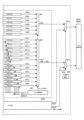
図2~図5は、実施例1の撮像素子100の全体構成図を4つに分割して示す図であり、図2は撮像素子の全体構成の内の左上部分の構成、図3は右上部分の構成、図4は左下部分の構成、図5は右下部分の構成を示す図である。
2 to 5 are diagrams showing the overall configuration of the
図2~図5に示すように、光電変換素子を有する画素200が一番左上の画素R0_0~一番右下の画素Bm-1_n-1(m、nは任意の整数)のように行列状に複数配置されている。画素200のそれぞれの表示R(G、B)p_qにおいて、Rは赤色、Gは緑色、Bは青色のカラーフィルタが各画素に配置されていることを意味する。図2~図5に示すようにカラーフィルタの配置はベイヤー配列となっている。
As shown in FIGS. 2 to 5,
また、各画素200の表示R(G,B)p_qにおいて、p_qは、第p行第q列の画素であることを示している。
ここで、画素200の画素の構成について図6を用いて説明する。図6は、撮像素子100内の画素200の構成例を示す回路図である。画素200は、フォトダイオード201a、201b、転送スイッチ202a、202b、フローティングディフュージョン領域203、増幅部204、リセットスイッチ205及び選択スイッチ206a、206bを有する。
Furthermore, in the display R(G,B)p_q of each
Here, the configuration of the
なお、各スイッチは、MOSトランジスタ等により構成される。以下の説明では、各スイッチは、一例としてN型のMOSトランジスタであるものとするが、各スイッチはP型のMOSトランジスタであってもよく、その他のスイッチング素子であってもよい。
このように、本実施例における撮像素子100は、1つの単位画素200内に、2つのフォトダイオード201a(第1の光電変換部)、201b(第2の光電変換部)を有する。
Note that each switch is composed of a MOS transistor or the like. In the following description, each switch is assumed to be an N-type MOS transistor as an example, but each switch may be a P-type MOS transistor or other switching element.
In this way, the
ただし、各単位画素200に設けられるフォトダイオードの個数は、図6に示されるような2つに限定されず、3つ以上(例えば、4つ)でもよい。本実施例において、フォトダイオード201a、201bは、後述するように、焦点検出画素として機能するとともに、撮像画素としても機能する。
フォトダイオード201a及び201bは、同一のマイクロレンズを通過した左右の異なる射出瞳からの光を受光し、光電変換によりその受光量に応じた信号電荷を生成する光電変換部である。
However, the number of photodiodes provided in each
The
フォトダイオード201aにより得られる信号を例えばA像信号、フォトダイオード201bにより得られる信号を例えばB像信号と呼ぶ。
転送スイッチ202aは、フォトダイオード201aとフローティングディフュージョン領域203との間に接続され、転送スイッチ202bはフォトダイオード201bとフローティングディフュージョン領域203との間に接続される。
The signal obtained by the
転送スイッチ202a及び202bは、それぞれ、フォトダイオード201a及び201bで発生した電荷を共通のフローティングディフュージョン領域203に転送する素子である。転送スイッチ202a及び202bは、それぞれ、制御信号txa及びtxbによって制御される。
フローティングディフュージョン領域203は、フォトダイオード201a及び201bから転送された電荷を一時的に保持するとともに、保持した電荷を電圧信号に変換する電荷電圧変換部である。増幅部204は、ソースフォロワ型MOSトランジスタである。増幅部204のゲートは、フローティングディフュージョン領域203に接続され、増幅部204のドレインは電源電位VDDを供給する共通の電源208に接続される。
The floating
増幅部204は、フローティングディフュージョン領域203に保持された電荷に基づく電圧信号を増幅して、画像信号として出力する。
リセットスイッチ205は、フローティングディフュージョン領域203と共通の電源208との間に接続される。
The
リセットスイッチ205は、制御信号resによって制御され、フローティングディフュージョン領域203の電位を電源電位VDDにリセットする。選択スイッチ206a、206bは、増幅部204のソースと列信号線300a~300lの間に接続される。選択スイッチ206a、206bは、それぞれ制御信号sel0、sel1によって制御され、増幅部204で増幅された画像信号を出力端子vout207a、207bに出力する。
The
図2~図5に戻り、垂直走査回路303は、制御信号res、txa、txb、sel0、sel1等を各画素200に供給する。これらの制御信号は、それぞれ各画素200の端子res、txa、txb、sel0、sel1に供給される。各画素の出力端子vout207a、207bは、列出力線300a~300lに接続される。画素R0_0が配置される縦の列(0列目)を例に説明すると、図2~図5に示すように0行目の画素R0_0からm-1行目の画素Gm-1_0までの画素と列出力線300a~300lが12行毎の周期で接続される。
Returning to FIGS. 2 to 5, the
本実施例では、12行毎の周期で、各行の出力端子207aは異なる列出力線300a~300lにそれぞれ接続されている。また、出力端子207bは一つおきの同色の3行ずつが同じ列出力線300a~300lに接続されている。この構成により、1水平期間毎に12行分のsel0をONにすることで12行分の画素信号を異なる列出力線に同時に出力することができる。
In this embodiment, the
また、12行分のsel1をONにすることで3行分ずつの画素信号を同じ列出力線に出力することによって信号を混合(加算)することができる。この接続パターンは、各列同様となっている。ただし、画素と列出力線の接続パターンはこの限りではない。 Furthermore, by turning on sel1 for 12 rows, the pixel signals for each three rows are output to the same column output line, thereby making it possible to mix (add) the signals. This connection pattern is the same for each column. However, the connection pattern between pixels and column output lines is not limited to this.
列出力線300a~300lは、それぞれ列回路としてのAD変換器(ADC)301a~301lの入力へ接続される。AD変換器301a~301lは、画素200から出力される光信号(S信号)とノイズ信号(N信号)をそれぞれアナログ-デジタル変換する。列出力線300a~300lには、それぞれ電流源302a~302lが接続されている。
電流源302a~302lと列出力線300a~300lに選択スイッチ206a、206bを介して接続された画素200の増幅MOSトランジスタからなる増幅部204によってソースフォロア回路が構成される。
ADC301a~301lは、ランプ信号発生器306a、306bやカウンタ305a、305bから出力される信号とTG(タイミングジェネレータ)307a、307bから出力される制御信号に基づき、列出力線300a~300lに出力された画素信号をAD変換する。
A source follower circuit is constituted by the
The
また、TG307a、307bからはADC301a~301lの各ADC別にパワーセーブ制御信号が入力される。このパワーセーブ制御信号がアサート(有効化)されると、ADC301a~301lはパワーセーブ状態になり、電力が動作時よりも低減される。
ここで実施例においてパワーセーブとは給電を停止または削減することである。
Further, power save control signals are input from the
In this embodiment, power saving means stopping or reducing power supply.
ADC301a~301lでAD変換されてデジタルデータとなった画素データは、水平走査回路304a、304bからの制御信号によって共通出力線324a、324b、325a、325bを介してメモリ308a、308bへ各列順次転送される(メモリ転送)。
メモリ308a、308bからは後述する動作により画素のSデータと、それに対応する画素のNデータがS-N演算部309a、309bへ出力される。
The pixel data converted into digital data by the
The
なお垂直走査回路303と水平走査回路304a、304bはCPU102と共に、画素からの信号を読出すための読出し手段として機能している。そして読出し手段として、第1の光電変換部の信号を列出力線に読出す第1の読出し動作と、第1及び第2の光電変換部の信号を混合した信号を列出力線に読出す第2の読出し動作を行う。
Note that the
S-N演算部309a、309bは、入力されたSデータからNデータを減算する。この動作により各画素の読出し回路に起因するノイズ成分をキャンセルした画像信号が生成される。
S-N演算部309a、309bから出力されたデータは、補正回路310a、310bに入力される。補正回路310a、310bではOBクランプなどの所定の補正処理が行われる。
The
The data output from the
補正回路310a、310bから出力されたデータはデータ出力部311a、311bに入力され、データ出力部311a、311bから撮像素子100の外部へデータが出力される。
S-N演算部309a、309b、補正回路310a、310bはTG307a、307bから出力される個別のパワーセーブ制御信号によりパワーセーブが制御される。
The data output from the
The power save of the
このパワーセーブ制御信号がアサート(有効化)されると、各回路はパワーセーブ状態になり、電力が動作時よりも低減される。
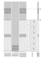
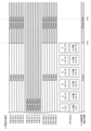
ここで、メモリ308a、308bの構成について図7、図8を用いて説明する。ここでは、例えばR画素の信号を格納するメモリ308aを例に説明する。
When this power save control signal is asserted (enabled), each circuit enters a power save state, and power consumption is reduced below that during operation.
The configuration of the
図7、図8は実施例1の撮像素子内のメモリ308aの構成を示す図であり、図7は撮像素子内のメモリ308aの左側部分の構成を示す図、図8は撮像素子内のメモリ308aの右側部分の構成を示す図である。
7 and 8 are diagrams showing the configuration of the
メモリ308aはメモリ群330a、330bで構成されている。各メモリ群はメモリN_0 340a~メモリN_5 340f、メモリA_0 341a~メモリA_5 341f、メモリAB_0 342a~メモリAB_5 342fで構成されている。各メモリは図8のメモリ制御部343から出力される書き込み制御信号、読出し制御信号によって制御され、それぞれ1行分の容量を有する。
The
ADC301a~301fから入力される各列のNデータはそれぞれ、メモリN_0 340a~メモリN_5 340fに書き込まれる。
また、各列のA像データはそれぞれメモリA_0 341a~メモリA_5 341fに書き込まれる。A像データとB像データの混合信号である各列のA+B像データはメモリAB_0 342a~メモリAB_5 342fに書き込まれる。
The N data of each column inputted from the
Further, the A image data of each column is written to the
各メモリに書き込まれた各信号は、メモリ制御部343から出力される読出し制御信号により順次読出される。また、メモリ制御部343から出力されるセレクト信号に従って動作するセレクタ344、345、図8の出力制御部332から出力されるセレクト信号に従って動作するセレクタ331a、331bを介してS-N演算部309aへ所定のメモリのNデータと所定のメモリのS信号(A像データ、A+B像データ)が出力される。
Each signal written in each memory is sequentially read out by a read control signal output from the
メモリ群330aとメモリ群330bの、出力制御部332から出力されるセレクト信号、またはメモリ制御部343の書き込み制御と読出し制御は、1水平期間毎に交互に切り替わる。例えば、ある水平期間ではメモリ群330aへ書き込むと同時にメモリ330bから読出しが行われ、別の水平期間ではメモリ群330bへ書き込むと同時にメモリ330aから読出しが行われる。
The select signal output from the output control section 332 or the write control and read control of the
この動作により、ある水平走査期間で12行を同時にAD変換しメモリ群330a(330b)に記憶すると共に、前の水平期間でAD変換しメモリ群330b(330a)に記憶した12行のデータをS-N演算して撮像素子から出力することができる。
また、メモリ群330aの、メモリN_0 340a~メモリN_5 340f、メモリA_0 341a~メモリA_5 341f、メモリAB_0 342a~メモリAB_5 342fはTG307aから出力される個別のパワーセーブ制御信号(PSAVE_MEM)によりパワーセーブが制御される。
Through this operation, 12 rows are simultaneously AD-converted and stored in the
In addition, power saving of the
このパワーセーブ制御信号がアサートされると、各メモリはパワーセーブ状態になり、電力が動作時よりも低減される。メモリ群330bについても同様に制御される。
ここで、撮像素子100の各モードでの読出し動作について説明する。
実施例1の撮像装置は撮影モードとして、動画モード1、動画モード2、動画モード3、静止画モードを具備する。
When this power save control signal is asserted, each memory enters a power save state, and the power is reduced compared to when it is in operation. The
Here, the readout operation in each mode of the
The imaging device of the first embodiment has a moving
図9~図12は、動画モード1の読出し動作を示すタイミングチャートである。
なお、図9は動画モード1における撮像素子の読出し動作を示すタイミングチャートの上半分を示す図であり、図10は動画モード1における撮像素子の読出し動作を示すタイミングチャートの下半分を示す図である。
9 to 12 are timing charts showing the read operation in moving
Note that FIG. 9 is a diagram showing the upper half of the timing chart showing the readout operation of the image sensor in
また図11は動画モード1におけるメモリの読出し動作を示すタイミングチャートの左側部分を示す図であり、図12は動画モード1におけるメモリの読出し動作を示すタイミングチャートの右側部分を示す図である。
以下、図9~図12を参照しつつ画像信号の12行分(1水平走査線分)の読出し動作について説明する。なお、各制御信号がHのときに各スイッチはオンになり、Lのときに各スイッチはオフになるものとする。
11 is a diagram showing the left side of a timing chart showing the memory read operation in
The readout operation for 12 lines (one horizontal scanning line) of image signals will be described below with reference to FIGS. 9 to 12. It is assumed that when each control signal is H, each switch is turned on, and when each control signal is L, each switch is turned off.
図9~図12を用いて、例えばR画素の読出し動作について説明するが、他の色についても同様の動作であり、説明は省略する。
図9、図10に示すように、時刻ta0において、制御信号txa_12k~txa_12k+10、txb_12k~txb_12k+10がHになり、転送スイッチ202a、202bがオンになる。
For example, the readout operation of an R pixel will be explained using FIGS. 9 to 12, but the operation is similar for other colors, and the explanation will be omitted.
As shown in FIGS. 9 and 10, at time ta0, control signals txa_12k to txa_12k+10 and txb_12k to txb_12k+10 become H, and
この時、信号res_12k~res_12k+10はHになっており、フォトダイオード201a、201bに蓄積された電荷は、転送スイッチ202a、202b、リセットスイッチ205を介して電源208に転送される。即ち、時刻ta0において、フォトダイオード201a、201bはリセットされる。次に、時刻ta1において、制御信号txa_12k~txa_12k+10、txb_12k~txb_12k+10をLとし、フォトダイオード201a、201bへの光電荷の蓄積が開始される。
At this time, the signals res_12k to res_12k+10 are at H level, and the charges accumulated in the
所定の時間だけ光電荷の蓄積を行った後の時刻ta3において、選択スイッチ206の制御信号sel0_12k~sel0_12k+10がHになり、増幅部204のソースが選択スイッチ206aを介して列出力線300a~300fに接続される。時刻ta4において、リセットスイッチ205の制御信号res_12k~res_12k+10をLとすることでフローティングディフュージョン領域203のリセットを解除する。
At time ta3 after photoelectric charges have been accumulated for a predetermined time, the control signals sel0_12k to sel0_12k+10 of the selection switch 206 become H, and the source of the
このとき、フローティングディフュージョン領域203の電位に応じたリセット信号レベルの電位(N信号)が増幅部204を介して列出力線300a~300fに読出され、AD変換器301a~301fに入力される。このように時刻ta4において、N信号(ノイズ信号)を読出すためのノイズ読出し動作が行われる。
次に、時刻ta5において、AD変換器301a~301fのパワーセーブ制御信号はネゲート(無効化)され、AD変換器301a~301fはアクティブになる。
At this time, a reset signal level potential (N signal) corresponding to the potential of the floating
Next, at time ta5, the power save control signals of the
ここで、TG307a、307bはCPU102と共にパワーセーブをするための制御手段として機能している。
ランプ信号発生器306aは時間経過に比例して信号レベルが変化するランプ信号の出力を開始する。同時にカウンタ305aはリセット状態からカウントアップを開始する。AD変換器301a~301f内の比較器において、入力信号とランプ信号発生器306aが出力するランプ信号とを比較する。
Here, the
The
入力されたランプ信号の信号レベルが時間の経過とともに大きくなり、その信号レベルが入力信号の値を上回った時点で、出力されているカウンタ値を記憶する。この記憶されたカウンタ値がNデータとなる(N信号のAD変換)。
時刻ta6において、N信号のAD変換が終了すると、各列のNデータがメモリ308aへ転送され、時刻ta7にて終了する。
The signal level of the input ramp signal increases over time, and when the signal level exceeds the value of the input signal, the output counter value is stored. This stored counter value becomes N data (AD conversion of N signal).
When the AD conversion of the N signal is completed at time ta6, the N data of each column is transferred to the
この時、AD変換器301a~301fの各列のNデータは例えばメモリ群330aの、それぞれメモリN_0 340a~メモリN_5 340fに送られることとなる。それに伴い、時刻ta6においては同時にAD変換器301c~301fのパワーセーブ制御信号がアサートされ、AD変換器301c~301fはパワーセーブ状態となる。
At this time, N data of each column of
次に、時刻ta8では、制御信号txa_12k~txa_12k+10がHになり、フォトダイオード201aの光電荷がそれぞれフローティングディフュージョン領域203へ転送される。その後、時刻ta9において、制御信号txa_12k~txa_12k+10がLになる。この動作により、フォトダイオード201a(第1の光電変換部)にta1~ta9の期間蓄積された電荷信号(A信号)がフローティングディフュージョン領域203へ転送される。
Next, at time ta8, the control signals txa_12k to txa_12k+10 become H, and the photocharges of the
そして、このとき選択スイッチ206の制御信号sel0_12k~sel0_12k+10がHなので、その変化に応じた電圧が増幅部204及び列出力線300a~300fに出力される。このように時刻ta9において、第1の光電変換部の信号(A像信号)を列出力線に読出すための第1の読出し動作が行われる。
At this time, since the control signals sel0_12k to sel0_12k+10 of the selection switch 206 are H, voltages corresponding to the changes are output to the
次に、時刻ta10において、ランプ信号発生器306aはランプ信号の出力を開始する。同時にカウンタ305aはリセット状態からカウントアップを開始する。AD変換器301a、301b内の比較器において、入力信号とランプ信号発生器306aが出力するランプ信号とを比較する。入力されたランプ信号の信号レベルが時間の経過とともに大きくなり、その信号レベルが入力信号の値を上回った時点で、出力されているカウンタ値を記憶する。
Next, at time ta10, the
この記憶されたカウンタ値がA像データとなる(A像信号のAD変換)。ただし、AD変換器301a、301bだけがアクティブなので、12k行と12k+2行のA像信号だけがAD変換されることになる。
時刻ta11において、A像信号のAD変換が終了すると、各列のA像データがメモリ308aへ転送され、時刻ta12にて終了する。
This stored counter value becomes A image data (AD conversion of A image signal). However, since only the
When AD conversion of the A-image signal is completed at time ta11, the A-image data of each column is transferred to the
この時、AD変換器301a、301bの各列のA像データはそれぞれメモリA_0 341a、メモリA_1 341bに格納されることとなる。しかしAD変換器301c~301fはパワーセーブ状態となっているため、有効なデータは出力されず、メモリ308aへもデータは格納されない。
At this time, the A image data of each column of the
時刻ta13において、再び制御信号txa_12k~txa_12k+10がHになるとともに制御信号txb_12k~txb_12k+10もHとなる。その後、時刻ta14において、制御信号txa_12k~txa_12k+10とtxb_12k~txb_12k+10がLになる。 At time ta13, the control signals txa_12k to txa_12k+10 become H again, and the control signals txb_12k to txb_12k+10 also become H. After that, at time ta14, the control signals txa_12k to txa_12k+10 and txb_12k to txb_12k+10 become L.
この動作により、フォトダイオード201a(第1の光電変換部)、201b(第2の光電変換部)の双方の電荷信号がともにフローティングディフュージョン領域203へ転送され加算(混合)されA+B像信号が生成される。そして、このとき選択スイッチ206の制御信号sel0_12k~sel0_12k+10がHなので、その変化に応じた電圧が増幅部204及び列出力線300a~300fに出力される。このように時刻ta14において、第1及び第2の光電変換部の信号を混合した信号(A+B像信号)を列出力線に読出すための第2の読出し動作が行われる。
Through this operation, the charge signals of both the
次に、時刻ta15において、AD変換器301c~301fのパワーセーブ制御信号はネゲート(無効化)され、AD変換器301c~301fはアクティブになる。ランプ信号発生器306aはランプ信号の出力を開始する。同時にカウンタ305aはリセット状態からカウントアップを開始する。AD変換器301a~301f内の比較器において、入力信号とランプ信号発生器306aが出力するランプ信号とを比較する。
Next, at time ta15, the power save control signals of the
入力されたランプ信号の信号レベルが時間の経過とともに大きくなり、その信号レベルが入力信号の値を上回った時点で、出力されているカウンタ値を記憶する。この記憶されたカウンタ値がA+B像データとなる(A+B像信号のAD変換)。
時刻ta16において、A+B像信号のAD変換が終了すると、各列のA+B像データがメモリ308aへ転送され、時刻ta19にて終了する。
The signal level of the input ramp signal increases over time, and when the signal level exceeds the value of the input signal, the output counter value is stored. This stored counter value becomes A+B image data (AD conversion of A+B image signal).
When AD conversion of the A+B image signal is completed at time ta16, the A+B image data of each column is transferred to the
この時、AD変換器301a~301fの各列のA+B像データはそれぞれメモリAB_0 342a~メモリAB_5 342fに格納されることとなる。
また、時刻ta16においては同時にAD変換器301a~301fのパワーセーブ制御信号がアサートされ、AD変換器301a~301fはパワーセーブ状態となる。
その後時刻ta17において制御信号res_12k~res_12k+10がH、時刻ta18において制御信号SEL0_12k~SEL0_12k+10がLになり12行分(1水平走査線分)の画素からの信号読出しとAD変換動作が完了する。
At this time, the A+B image data of each column of the
Further, at time ta16, the power save control signals of the
Thereafter, at time ta17, the control signals res_12k to res_12k+10 become H, and at time ta18, the control signals SEL0_12k to SEL0_12k+10 become L, completing the signal reading from the pixels of 12 rows (one horizontal scanning line) and the AD conversion operation.
図9、図10に示す時刻ta2から時刻ta20の期間では、メモリ308aのメモリ群330bに既に格納されているデータ(前の水平期間でAD変換されたデータ)がメモリ308aから出力され、データ出力部311aを介して撮像素子100外へ出力される。上述した時刻ta2から時刻ta20までの期間を、読出しの単位である1水平期間とする。
In the period from time ta2 to time ta20 shown in FIGS. 9 and 10, data already stored in the
AD変換され、メモリ308aのメモリ群330aにデータが格納された後、メモリ群330aからデータ出力部311aを介して出力されるまでの動作のタイミングチャートを図11、図12に示す。図11は動画モード1におけるメモリ群330aへの書き込み、読出し動作を示すタイミングチャートの左側部分を示す図であり、図12は右側部分を示す図である。
図11、図12において、図9、図10と同じ時刻が記載されているタイミングは、図9、図10と同じタイミングであることを示す。
FIGS. 11 and 12 show timing charts of operations from AD conversion and storage of data in the
In FIGS. 11 and 12, timings in which the same times as those in FIGS. 9 and 10 are described are the same timings as in FIGS. 9 and 10.
時刻ta6ではメモリ群330aのメモリN_0 340a~メモリN_5 340fのパワーセーブ制御信号はネゲートされ、メモリが動作状態となると共に、NデータのメモリN_0 340a~メモリN_5 340fへの書き込みが開始される。時刻ta7にて書き込みが終了するとパワーセーブ制御信号はアサートされ、メモリはパワーセーブ状態となる。パワーセーブ状態ではメモリ内のデータは保持される。
At time ta6, the power save control signals of the
時刻ta11ではメモリ群330aのメモリA_0 341a~メモリA_1 341bのパワーセーブ制御信号はネゲートされ、メモリが動作状態となるとともに、A像データのメモリA_0 341a、メモリA_1 341bへの書き込みが開始される。時刻ta12にて書き込みが終了するとパワーセーブ制御信号はアサートされ、メモリはパワーセーブ状態となる。メモリA_2 341c~メモリA_5 341fにはデータの書き込みが行われないため、パワーセーブ制御信号はアサートのままであり、パワーセーブ状態のままを保つ。
At time ta11, the power save control signals of
時刻ta16ではメモリAB_0 342a~メモリAB_5 342fのパワーセーブ制御信号はネゲートされ、メモリが動作状態となるとともに、A+B像データのメモリAB_0 342a~メモリAB_5 342fへの書き込みが開始される。時刻ta19にて書き込みが終了するとパワーセーブ制御信号はアサートされ、メモリはパワーセーブ状態となる。
At time ta16, the power save control signals of
次の水平期間の時刻ta2では、メモリ群330aのメモリN_0 340a~メモリN_5 340f、メモリA_0 341a、メモリA_1 341b、メモリAB_0 342a~メモリAB_5 342fのパワーセーブ制御信号がネゲートされ、これらのメモリが動作状態となる。メモリA_2 341c~メモリA_5 341fについては、パワーセーブ制御信号はアサートのままであり、パワーセーブ状態のままを保つ。
At time ta2 of the next horizontal period, the power save control signals of
この状態でメモリ制御部343と出力制御部332により、図12に示すように、12k、12k+2行のA像データと、12k、12k+2、12k+4、12k+6、12k+8、12k+10行のNデータとA+B像データがメモリ308aから出力される。
この間S-N演算部309aと補正回路310aはパワーセーブ制御信号がネゲートされており、動作状態となっている。
In this state, the
During this time, the power save control signal is negated in the
S-N演算部309aでA像データ-Nデータ、または(A+B)像データ-Nデータが出力され、補正回路310aでの処理の後、データ出力部311aから撮像素子100外へ出力される。
なお、上記の(A+B)像データ-Nデータは、後述するように、図25のステップS103において、表示部104で動画として画像表示される。また、A像データ-Nデータと演算されてB像データを生成し、A像データとB像データを用いて位相差焦点検出が実行される。即ち、例えばステップS103は位相差焦点検出手段として機能している。
A image data-N data or (A+B) image data-N data is outputted by the
Note that the above (A+B) image data -N data is displayed as a moving image on the
時刻ta20にて出力が完了されると、メモリ308a、S-N演算部309a、補正回路310aのパワーセーブ制御信号はすべてアサートされ、各回路がパワーセーブ状態となる。
この時刻ta0~ta20の動作を12行ずつ所定数の水平走査線分繰り返すことにより1画面分の像信号を取得する。
When the output is completed at time ta20, the power save control signals of the
By repeating this operation from time ta0 to time ta20 for a predetermined number of horizontal scanning lines every 12 rows, image signals for one screen are obtained.
以上のように、TG307a、307b、CPU102は、第2の読出し動作に使用する列回路のうち、第1の読出し動作の際に使用しない少なくとも一部の列回路を、第1の読出し動作の際にパワーセーブする制御手段として機能している。
また制御手段は、第2の読出し動作の際に使用しない列回路も、第1の読出し動作の際にパワーセーブしている。
As described above, the
The control means also saves the power of column circuits that are not used during the second read operation during the first read operation.
なお、実施例においては第1の読出し動作の際に読出される行の数は、第2の読出し動作の際に読出される行の数より少なく設定されている。
また、実施例においては、複数の画素からノイズ信号を読出すノイズ読出し動作を有し、第1の読出し動作の際にパワーセーブする列回路をノイズ読出し動作終了時からパワーセーブするように構成されている。
Note that in the embodiment, the number of rows read during the first read operation is set to be smaller than the number of rows read during the second read operation.
Further, the embodiment has a noise readout operation for reading out noise signals from a plurality of pixels, and the column circuit that saves power during the first readout operation is configured to save power from the end of the noise readout operation. ing.
また、ノイズ読出し動作終了時から第2の読出し動作開始まで列回路に対するパワーセーブ状態と非パワーセーブ状態を変更しないように構成されている。従って、第2の読出し動作開始時にパワーセーブ状態から非パワーセーブ状態に変化することがなく、立ち上がりによる遅延が発生しにくくなっている。
また、実施例では、パワーセーブする列回路から出力されるデータをそれぞれ格納するための対応するメモリを有し、列回路のパワーセーブに伴って対応するメモリもパワーセーブしている。
Further, the configuration is such that the power save state and non-power save state for the column circuits are not changed from the end of the noise read operation to the start of the second read operation. Therefore, there is no change from the power save state to the non-power save state at the start of the second read operation, making it difficult for delays due to rise to occur.
Further, in the embodiment, there is provided a corresponding memory for storing data outputted from each column circuit whose power is to be saved, and when the power of the column circuit is saved, the power of the corresponding memory is also saved.
図13~16は、実施例1の動画モード2の読出し動作を示すタイミングチャートである。
図13は実施例1の動画モード2における撮像素子の読出し動作を示すタイミングチャートの上半分を示す図であり、図14は実施例1の動画モード2における撮像素子の読出し動作を示すタイミングチャートの下半分を示す図である。
13 to 16 are timing charts showing the read operation in moving
FIG. 13 is a diagram showing the upper half of a timing chart showing the readout operation of the image sensor in
図15は実施例1の動画モード2におけるメモリへの書き込み、読出し動作を示すタイミングチャートの左側部分を示す図であり、図16は実施例1の動画モード2におけるメモリへの書き込み、読出し動作を示すタイミングチャートの右側部分を示す図である。
FIG. 15 is a diagram showing the left side of a timing chart showing write and read operations to the memory in
以下、図13~16を参照しつつ画像信号の12行分(1水平走査線分)の読出し動作について説明する。なお、図13~16は例としてR画素の読出し動作について説明するが、他の色についても同様の動作であり、説明を省略する。
時刻tb0において、制御信号txa_12k~txa_12k+10、txb_12k~txb_12k+10がHになり、転送スイッチ202a、202bがオンになる。
The readout operation for 12 lines (one horizontal scanning line) of image signals will be described below with reference to FIGS. 13 to 16. Note that although FIGS. 13 to 16 will explain the readout operation of the R pixel as an example, the operation is similar for other colors, and the explanation will be omitted.
At time tb0, control signals txa_12k to txa_12k+10 and txb_12k to txb_12k+10 become H, and
この時、信号res_12k~res_12k+10はHになっており、フォトダイオード201a,201bに蓄積された電荷は、転送スイッチ202a、202b、リセットスイッチ205を介して電源208に転送され、フォトダイオード201a、201bの電荷はリセットされる。
時刻tb1において、制御信号txa_12k~txa_12k+10、txb_12k~txb_12k+10をLとし、フォトダイオード201a、201bにおける光電荷の蓄積が開始される。
At this time, the signals res_12k to res_12k+10 are H, and the charges accumulated in the
At time tb1, the control signals txa_12k to txa_12k+10 and txb_12k to txb_12k+10 are set to L, and accumulation of photocharges in the
所定の時間だけ光電荷の蓄積を行った後の時刻tb3において、選択スイッチ206の制御信号sel1_12k~sel1_12k+10がHになり、増幅部204のソースが選択スイッチ206bを介して列出力線300a~300fに接続される。
尚、図9、図10では選択スイッチ206aの制御信号sel0_12k~sel0_12k+10をHにしているのに対して、図13、図14では選択スイッチ206bの制御信号sel1_12k~sel1_12k+10をHにしている。従って、各画素出力が接続される列出力線が異なる。
At time tb3 after the photocharge has been accumulated for a predetermined time, the control signals sel1_12k to sel1_12k+10 of the selection switch 206 become H, and the source of the
Note that in FIGS. 9 and 10, the control signals sel0_12k to sel0_12k+10 of the
時刻tb4において、リセットスイッチ205の制御信号res_12k~res_12k+10をLとすることでフローティングディフュージョン領域203のリセットを解除する。このとき、選択スイッチ206の制御信号sel1_12k~sel1_12k+10がHなので、フローティングディフュージョン領域203の電位に応じたリセット信号レベルの電位(N信号)が増幅部204を介して列出力線300aと300bだけに読出される。
At time tb4, the reset of the floating
次に、時刻tb5において、AD変換器301a~301bのパワーセーブ制御信号はネゲートされ、AD変換器301a~301bはアクティブになる。ただし、AD変換器301c~301fはパワーセーブ状態のままとする。
ランプ信号発生器306aは時間経過に比例して信号レベルが変化するランプ信号の出力を開始する。同時にカウンタ305aはリセット状態からカウントアップを開始する。
Next, at time tb5, the power save control signals of
The
AD変換器301a~301b内の比較器において、入力信号とランプ信号発生器306aが出力するランプ信号とを比較する。入力されたランプ信号の信号レベルが時間の経過とともに大きくなり、その信号レベルが入力信号の値を上回った時点で、出力されているカウンタ値を記憶する。この記憶されたカウンタ値がNデータとなる(N信号のAD変換)。
Comparators in the
この時、列出力線300aに出力された12k、12k+2行、12k+4行のN信号の加算信号がAD変換器301aによりAD変換される。また列出力線300bに出力された12k+6、12k+8行、12k+10行のN信号の加算信号がAD変換器301bによりAD変換される。
At this time, the summed signals of the N signals of
時刻tb6において、N信号のAD変換が終了すると、各列のNデータがメモリ308aへ転送され、時刻tb7にて終了する。この時、AD変換器301aからの12k、12k+2行、12k+4行の加算されたNデータがメモリN_0 340aに格納され、AD変換器301bからの12k+6、12k+8行、12k+10行の加算されたNデータがメモリN_1 340bに格納されることとなる。
When the AD conversion of the N signal is completed at time tb6, the N data of each column is transferred to the
また、時刻tb6においては同時にAD変換器301bのパワーセーブ制御信号がアサートされ、AD変換器301bはパワーセーブ状態となる。
時刻tb8~tb9に、制御信号txa_12k~txa_12k+10がHになり、この動作により、フォトダイオード201aに蓄積された電荷がフローティングディフュージョン領域203へ転送される。そして、このとき選択スイッチ206の制御信号sel1_12k~sel1_12k+10がHなので、その変化に応じた電圧が増幅部204及び列出力線300aと300bだけに読出される。
Further, at time tb6, the power save control signal of the
At times tb8 to tb9, the control signals txa_12k to txa_12k+10 become H, and by this operation, the charges accumulated in the
次に、時刻tb10において、AD変換器301aだけがアクティブにされ、ランプ信号発生器306aはランプ信号の出力を開始する。同時にカウンタ305aはリセット状態からカウントアップを開始する。AD変換器301a内の比較器において、入力信号とランプ信号発生器306aが出力するランプ信号とを比較する。入力されたランプ信号の信号レベルが時間の経過とともに大きくなり、その信号レベルが入力信号の値を上回った時点で、出力されているカウンタ値を記憶する。この記憶されたカウンタ値がA像データとなる(A像信号のAD変換)。
Next, at time tb10, only the
従って、列出力線300aに出力された12k、12k+2行、12k+4行のA像信号の加算信号だけがAD変換器301aによりAD変換される。なお、このように、動画モード2では、第1の読出し動作の際に複数行の信号を加算して列出力線に読出している。
時刻tb11において、A像信号のAD変換が終了すると、AD変換器301aのA像データがメモリ308aへ転送され、時刻tb12にて終了する。この時、AD変換器301aのA像データはメモリA_0 341aに格納されることとなる。
Therefore, only the addition signal of the A image signals of
When the AD conversion of the A image signal is completed at time tb11, the A image data of the
AD変換器301b~301fはパワーセーブ状態となっているため、有効なデータは出力されず、メモリ308aへもデータは格納されない。
時刻tb13~tb14において、再び制御信号txa_12k~txa_12k+10がHになるとともに制御信号txb_12k~txb_12k+10もHとなる。この動作により、フォトダイオード201a、201bの双方の光電荷がともにフローティングディフュージョン領域203へ転送され加算されA+B像信号が生成される。そして、その変化に応じた電圧が増幅部204及び列出力線300aと300bだけに出力される。
Since the
At times tb13 to tb14, the control signals txa_12k to txa_12k+10 become H again, and the control signals txb_12k to txb_12k+10 also become H. Through this operation, the photocharges of both
次に、時刻tb15において、AD変換器301bのパワーセーブ制御信号がネゲートされ、AD変換器301bはアクティブになる。ランプ信号発生器306aはランプ信号の出力を開始する。同時にカウンタ305aはリセット状態からカウントアップを開始する。AD変換器301a~301b内の比較器において、入力信号とランプ信号発生器306aが出力するランプ信号とを比較する。入力されたランプ信号の信号レベルが時間の経過とともに大きくなり、その信号レベルが入力信号の値を上回った時点で、出力されているカウンタ値を記憶する。
Next, at time tb15, the power save control signal of
この記憶されたカウンタ値がA+B像データとなる(A+B像信号のAD変換)。
これによって列出力線300aに出力された12k、12k+2行、12k+4行のA+B像信号の加算信号がAD変換器301aによりAD変換される。また、列出力線300bに出力された12k+6、12k+8行、12k+10行のA+B像信号の加算信号がAD変換器301bによりAD変換される。
This stored counter value becomes A+B image data (AD conversion of A+B image signal).
As a result, the summed signals of the A+B image signals of
時刻tb16において、A+B像信号のAD変換が終了すると、A+B像データがメモリ308aへ転送され、時刻tb19にて終了する。この時、AD変換器301aからの12k、12k+2行、12k+4行の加算されたA+B像データがメモリAB_0 342aに格納される。また、AD変換器301aからの12k+6、12k+8行、12k+10行の加算されたA+B像データがメモリAB_1 342bに格納される。
When AD conversion of the A+B image signal is completed at time tb16, the A+B image data is transferred to the
また、時刻tb16においては同時にAD変換器301a~301bのパワーセーブ制御信号がアサートされ、AD変換器301a~301bはパワーセーブ状態となる。
その後時刻tb17において制御信号res_12k~res_12k+10がH、時刻tb18において制御信号sel1_12k~sel1_12k+10がLになり12行分(1水平走査線分)の画素からの信号読出しとAD変換動作が完了する。
Further, at time tb16, the power save control signals of the
Thereafter, at time tb17, the control signals res_12k to res_12k+10 become H, and at time tb18, the control signals sel1_12k to sel1_12k+10 become L, completing signal reading from pixels of 12 rows (one horizontal scanning line) and AD conversion operation.
図13、図14の時刻tb2~tb20の期間では、メモリ308aの例えばメモリ群330bに既に格納されているデータ(後述する、前の水平期間でAD変換されたデータ)が出力され、データ出力部311aを介して撮像素子100外へ出力される。なお、上述した時刻tb2から時刻tb20までの期間を読出しの単位である、1水平期間とする。
In the period from time tb2 to tb20 in FIGS. 13 and 14, data already stored in, for example, the
AD変換され、メモリ308aのメモリ群330aに格納されたデータがデータ出力部311aから出力されるまでの動作のタイミングチャートを図15、図16に示す。図13、図14と同じ時刻が記載されているタイミングは、図13、図14と同じタイミングであることを示す。
FIGS. 15 and 16 show timing charts of operations until data that has been AD converted and stored in the
時刻tb6では同時にメモリN_0 340a~メモリN_1 340bのパワーセーブ制御信号はネゲートされ、メモリが動作状態となるとともに、メモリ群330aのNデータのメモリN_0 340a~メモリN_1 340bへの書き込みが開始される。
時刻tb7にて書き込みが終了するとパワーセーブ制御信号はアサートされ、メモリはパワーセーブ状態となる。パワーセーブ状態ではメモリ内のデータは保持される。メモリN_2 340c~メモリN_5 340fにはデータの書き込みが行われないため、パワーセーブ制御信号はアサートのままであり、パワーセーブ状態のままを保つ。
At time tb6, the power save control signals of the
When writing ends at time tb7, the power save control signal is asserted and the memory enters the power save state. In the power save state, data in memory is retained. Since no data is written to the
時刻tb11ではメモリA_0 341aのパワーセーブ制御信号はネゲートされ、メモリが動作状態となるとともに、A像データのメモリA_0 341aへの書き込みが開始される。時刻tb12にて書き込みが終了するとパワーセーブ制御信号はアサートされ、メモリはパワーセーブ状態となる。メモリA_1 341b~メモリA_5 341fにはデータの書き込みが行われないため、パワーセーブ制御信号はアサートのままであり、パワーセーブ状態のままを保つ。
At time tb11, the power save control signal of the
時刻tb16ではメモリAB_0 342a~メモリAB_1 342bのパワーセーブ制御信号はネゲートされ、メモリが動作状態となるとともに、A+B像データのメモリAB_0 342a~メモリAB_1 342bへの書き込みが開始される。時刻tb19にて書き込みが終了するとパワーセーブ制御信号はアサートされ、メモリはパワーセーブ状態となる。メモリAB_2 342c~メモリAB_5 342fにはデータの書き込みが行われないため、パワーセーブ制御信号はアサートのままであり、パワーセーブ状態のままを保つ。
At time tb16, the power save control signals of the
次の水平期間の時刻tb2では、メモリN_0 340a~メモリN_1 340b、メモリA_0 341a、メモリAB_0 342a~メモリAB_1 342bのパワーセーブ制御信号がネゲートされ、動作状態となる。メモリN_2 340c~メモリN_5 340f、メモリA_1 341b~メモリA_5 341f、メモリAB_2 342c~メモリAB_5 342fについては、パワーセーブ制御信号はアサートのままであり、パワーセーブ状態のままを保つ。
At time tb2 of the next horizontal period, the power save control signals of
この状態でメモリ制御部343と出力制御部332により、図16に示すように、12k、12k+2行、12k+4行の加算されたNデータと、加算されたA像データと、加算されたA+B像データがメモリ308aから出力される。また、12k+6、12k+8行、12k+10行の加算されたNデータとと、加算されたA+B像データがメモリ308aから出力される。この間S-N演算部309aと補正回路310aはパワーセーブ制御信号がネゲートされており、動作状態となっている。
In this state, the
S-N演算部309aによって加算されたA像データから加算されたNデータを減算すると共に、加算されたA+B像データから加算されたNデータを減算する。その後、補正回路310aでの処理の後、データ出力部311aから撮像素子100外へ出力される。
これらの信号は後述する図25のステップS108において、Nデータを減算したA+B像データは動画像として表示等に用いられ、更にNデータを減算したA像データを引くことによってB像データを算出する。そしてA像データとB像データの位相差に基づき焦点検出を行う。
The
In step S108 of FIG. 25, which will be described later, the A+B image data obtained by subtracting N data from these signals is used for display, etc. as a moving image, and B image data is calculated by further subtracting the A image data obtained by subtracting N data. . Then, focus detection is performed based on the phase difference between the A image data and the B image data.
時刻tb21にて出力が完了されると、メモリ308a、S-N演算部309a、補正回路310aのパワーセーブ制御信号はすべてアサートされ、各回路がパワーセーブ状態となる。
この時刻tb0~tb20の動作を12行ずつ所定数の水平走査線分繰り返すことにより1画面分の像信号を取得する。
When the output is completed at time tb21, the power save control signals of the
By repeating this operation from time tb0 to tb20 for a predetermined number of horizontal scanning lines every 12 rows, image signals for one screen are obtained.
次に、図17~図20は、実施例1の動画モード3の読出し動作を示すタイミングチャートである。
図17は実施例1の動画モード3における撮像素子の読出し動作を示すタイミングチャートの上半分を示す図であり、図18は実施例1の動画モード3における撮像素子の読出し動作を示すタイミングチャートの下半分を示す図である。
Next, FIGS. 17 to 20 are timing charts showing the read operation in moving
FIG. 17 is a diagram showing the upper half of a timing chart showing the readout operation of the image sensor in
図19は実施例1の動画モード3におけるメモリへの書き込み、読出し動作を示すタイミングチャートの左側部分を示す図であり、図20は実施例1の動画モード3におけるメモリへの書き込み、読出し動作を示すタイミングチャートの右側部分を示す図である。
以下、図17~図20を参照しつつ画像信号の12行分(1水平走査線分)の同時読出し動作について説明する。図17~図20では例としてR画素の読出し動作について説明する。他の色についても同様の動作であり、説明を省略する。
FIG. 19 is a diagram showing the left side of a timing chart showing write and read operations to the memory in
The simultaneous readout operation of 12 lines (one horizontal scanning line) of image signals will be described below with reference to FIGS. 17 to 20. In FIGS. 17 to 20, a readout operation of an R pixel will be described as an example. The operation is similar for other colors, and the explanation will be omitted.
なお、動画モード2と動画モード3は撮像素子100の各画素の駆動制御等は同じであり、A像信号を読出す際にAD変換器301bもアクティブにしている点が異なる。
時刻tc0において、制御信号txa_12k~txa_12k+10、txb_12k~txb_12k+10がHになり、転送スイッチ202a、202bがオンになる。この時、信号res_12k~res_12k+10はHになっており、フォトダイオード201a、201bに蓄積された電荷は、転送スイッチ202a、202b、リセットスイッチ205を介して電源208に転送される。そして、フォトダイオード201a、201bはリセットされる。
Note that the moving
At time tc0, the control signals txa_12k to txa_12k+10 and txb_12k to txb_12k+10 become H, and the transfer switches 202a and 202b are turned on. At this time, the signals res_12k to res_12k+10 are at H level, and the charges accumulated in the
時刻tc1において、制御信号txa_12k~txa_12k+10、txb_12k~txb_12k+10をLとし、フォトダイオード201a、201bへの光電荷の蓄積が開始される。
所定の時間だけ光電荷の蓄積を行った後の時刻tc3において、選択スイッチ206の制御信号sel1_12k~sel1_12k+10がHになり、増幅部204のソースが列出力線300a~300bに接続される。
At time tc1, control signals txa_12k to txa_12k+10 and txb_12k to txb_12k+10 are set to L, and accumulation of photocharges in the
At time tc3 after photoelectric charges have been accumulated for a predetermined period of time, the control signals sel1_12k to sel1_12k+10 of the selection switches 206 become H, and the sources of the
時刻tc4において、リセットスイッチ205の制御信号res_12k~res_12k+10をLとすることでフローティングディフュージョン領域203のリセットを解除する。このとき、フローティングディフュージョン領域203の電位に応じたリセット信号レベルの電位が増幅部204を介して列出力線300a、300bに読出され、AD変換器301a~301bに入力される。
At time tc4, the reset of the floating
次に、時刻tc5において、AD変換器301a、301bのパワーセーブ制御信号をネゲートし、AD変換器301a、301bをアクティブにする。ランプ信号発生器306aは時間経過に比例して信号レベルが変化するランプ信号の出力を開始する。同時にカウンタ305aはリセット状態からカウントアップを開始する。AD変換器301a、301b内の比較器において、入力信号とランプ信号発生器306aが出力するランプ信号とを比較する。
Next, at time tc5, the power save control signals of the
入力されたランプ信号の信号レベルが時間の経過とともに大きくなり、その信号レベルが入力信号の値を上回った時点で、出力されているカウンタ値を記憶する。この記憶されたカウンタ値がNデータとなる(N信号のAD変換)。
時刻tc6において、N信号のAD変換が終了すると、各列のNデータがメモリ308aへ転送され、時刻tc7にて終了する。この時、AD変換器301a、301bのNデータはそれぞれメモリN_0 340a~メモリN_1 340bに格納されることとなる。
The signal level of the input ramp signal increases over time, and when the signal level exceeds the value of the input signal, the output counter value is stored. This stored counter value becomes N data (AD conversion of N signal).
When the AD conversion of the N signal is completed at time tc6, the N data of each column is transferred to the
時刻tc8では、制御信号txa_12k~txa_12k+10がHになり、フォトダイオード201aの光電荷がフローティングディフュージョン領域203へ転送される。その後、時刻tc9において、制御信号txa_12k~txa_12k+10がLになる。この動作により、フォトダイオード201aに蓄積された電荷がフローティングディフュージョン領域203へ転送される。そして、その変化に応じた電圧が増幅部204及び列出力線300a、300bに出力される。
At time tc8, the control signals txa_12k to txa_12k+10 become H, and the photocharges of the
次に、時刻tc10において、ランプ信号発生器306aはランプ信号の出力を開始する。同時にカウンタ305aはリセット状態からカウントアップを開始する。AD変換器301a、301b内の比較器において、入力信号とランプ信号発生器306aが出力するランプ信号とを比較する。入力されたランプ信号の信号レベルが時間の経過とともに大きくなり、その信号レベルが入力信号の値を上回った時点で、出力されているカウンタ値を記憶する。この記憶されたカウンタ値がA像データとなる(A像信号のAD変換)。
Next, at time tc10, the
時刻tc11において、A像信号のAD変換が終了すると、各列のA像データがメモリ308aへ転送され、時刻tc12にて終了する。この時、AD変換器301a、301bのA像データはそれぞれメモリA_0 341a、A_1 341bに格納されることとなる。AD変換器301c~301fはパワーセーブ状態となっているため、有効なデータは出力されず、メモリ308aへもデータは格納されない。
At time tc11, when AD conversion of the A image signal is completed, each column of A image data is transferred to the
時刻tc13~tc14において、再び制御信号txa_12k~txa_12k+10がHになるとともに制御信号txb_12k~txb_12k+10もHとなる。この動作により、フォトダイオード201a、201bの双方の光電荷がともにフローティングディフュージョン領域203へ転送され加算される。そして、その変化に応じた電圧が増幅部204及び列出力線300a、300bに出力される。
At times tc13 to tc14, the control signals txa_12k to txa_12k+10 become H again, and the control signals txb_12k to txb_12k+10 also become H. Through this operation, both photocharges of the
次に、時刻tc15において、ランプ信号発生器306aはランプ信号の出力を開始する。同時にカウンタ305aはリセット状態からカウントアップを開始する。AD変換器301a、301b内の比較器において、入力信号とランプ信号発生器306aが出力するランプ信号とを比較する。入力されたランプ信号の信号レベルが時間の経過とともに大きくなり、その信号レベルが入力信号の値を上回った時点で、出力されているカウンタ値を記憶する。この記憶されたカウンタ値がA+B像データとなる(A+B像信号のAD変換)。
Next, at time tc15, the
時刻tc16において、A+B像信号のAD変換が終了すると、各列のA+B像データがメモリ308aへ転送され、時刻tc19にて終了する。この時、AD変換器301a、301bのA+B像データはそれぞれメモリAB_0 342a~メモリAB_1 342bに格納されることとなる。
また、時刻tc16においては同時にAD変換器301a、301bのパワーセーブ制御信号がアサートされ、AD変換器301a、301bはパワーセーブ状態となる。
When AD conversion of the A+B image signal is completed at time tc16, the A+B image data of each column is transferred to the
Further, at time tc16, the power save control signals of the
その後時刻tc17において制御信号res_12k~res_12k+10がH、時刻tc18において制御信号sel1_12k~sel1_12k+10がLになり12行分(1水平走査線分)の画素からの信号読出しとAD変換動作が完了する。 Thereafter, at time tc17, the control signals res_12k to res_12k+10 become H, and at time tc18, the control signals sel1_12k to sel1_12k+10 become L, completing signal reading from pixels of 12 rows (one horizontal scanning line) and AD conversion operation.
図17、図18に示す時刻tc2から時刻tc20の期間では、メモリ308aに既に格納されているデータ(後述する、前の水平期間でAD変換されたデータ)がメモリ308aから出力され、データ出力部311aを介して撮像素子100外へ出力される。上述した時刻tc2から時刻tc20までの期間を、読出しの単位である、1水平期間とする。
In the period from time tc2 to time tc20 shown in FIGS. 17 and 18, data already stored in the
AD変換され、メモリ308aに格納されたデータがデータ出力部311aから出力されるまでの動作のタイミングチャートを図19、図20に示す。図17、図18と同じ時刻が記載されているタイミングは、図17、図18と同じタイミングであることを示す。
時刻tc6ではメモリN_0 340a~メモリN_1 340bのパワーセーブ制御信号はネゲートされ、メモリが動作状態となるとともに、NデータのメモリN_0 340a~メモリN_1 340bへの書き込みが開始される。
FIGS. 19 and 20 show timing charts of operations until data that has been AD converted and stored in the
At time tc6, the power save control signals of
時刻tc7にて書き込みが終了するとパワーセーブ制御信号はアサートされ、メモリはパワーセーブ状態となる。パワーセーブ状態ではメモリ内のデータは保持される。メモリN_2 340c~メモリN_5 340fにはデータの書き込みが行われないため、パワーセーブ制御信号はアサートのままであり、パワーセーブ状態のままを保つ。
When writing ends at time tc7, the power save control signal is asserted and the memory enters the power save state. In the power save state, data in memory is retained. Since no data is written to the
時刻tc11ではメモリA_0 341a~メモリA_1 341bのパワーセーブ制御信号はネゲートされ、メモリが動作状態となるとともに、A像データのメモリA_0 341a~メモリA_1 341bへの書き込みが開始される。時刻tc12にて書き込みが終了するとパワーセーブ制御信号はアサートされ、メモリはパワーセーブ状態となる。メモリA_2 341c~メモリA_5 341fにはデータの書き込みが行われないため、パワーセーブ制御信号はアサートのままであり、パワーセーブ状態のままを保つ。
At time tc11, the power save control signals of
時刻tc16ではメモリAB_0 342a~メモリAB_1 342bのパワーセーブ制御信号はネゲートされ、メモリが動作状態となるとともに、NデータのメモリAB_0 342a~メモリAB_1 342bへの書き込みが開始される。時刻tc19にて書き込みが終了するとパワーセーブ制御信号はアサートされ、メモリはパワーセーブ状態となる。メモリAB_2 342c~メモリAB_5 342fにはデータの書き込みが行われないため、パワーセーブ制御信号はアサートのままであり、パワーセーブ状態のままを保つ。
At time tc16, the power save control signals of the
次の水平期間の時刻tc2では、メモリN_0 340a~メモリN_1 340b、メモリA_0 341a~メモリA_1 341b、メモリAB_0 342a~メモリAB_1 342bのパワーセーブ制御信号がネゲートされ、動作状態となる。メモリN_2 340c~メモリN_5 340f、メモリA_2 341c~メモリA_5 341f、メモリAB_2 342c~メモリAB_5 342fについては、パワーセーブ制御信号はアサートのままであり、パワーセーブ状態のままを保つ。
At time tc2 of the next horizontal period, the power save control signals of
この状態でメモリ制御部343と出力制御部332により、図20に示すように、12k、12k+2行、12k+4行のNデータを加算したデータと、A像データを加算したデータと、A+B像データを加算したデータとがメモリ308aから得られる。また、12k+6、12k+8行、12k+10行のNデータを加算したデータと、A像データを加算したデータと、A+B像データを加算したデータとがメモリ308aから得られる。この間S-N演算部309aと補正回路310aはパワーセーブ制御信号がネゲートされており、動作状態となっている。
In this state, the
S-N演算部309aと補正回路310aでの処理の後、データ出力部311aから撮像素子100外へ出力される。なお、後述する図25のステップS111において、Nデータを引いたA+B像データは動画表示等に用いられるとともに、Nデータを引いたA像データを演算してB像データを取得し、A像データとB像データの位相差に基づき焦点調整動作が行われる。
After processing in the
時刻tc21にて出力が完了されると、メモリ308a、S-N演算部309a、補正回路310aのパワーセーブ制御信号はすべてアサートされ、各回路がパワーセーブ状態となる。
この時刻tc0~tc20の動作を12行ずつ所定数の水平走査線分繰り返すことにより1画面分の像信号を取得する。
When the output is completed at time tc21, the power save control signals of the
By repeating this operation from time tc0 to tc20 for a predetermined number of horizontal scanning lines every 12 rows, image signals for one screen are obtained.
次に、図21~図24は、静止画モードの読出し動作を示すタイミングチャートである。
図21は静止画モードにおける撮像素子の読出し動作を示すタイミングチャートの上半分を示す図であり、図22は静止画モードにおける撮像素子の読出し動作を示すタイミングチャートの下半分を示す図である。
Next, FIGS. 21 to 24 are timing charts showing the read operation in still image mode.
FIG. 21 is a diagram showing the upper half of a timing chart showing the readout operation of the image sensor in the still image mode, and FIG. 22 is a diagram showing the lower half of the timing chart showing the readout operation of the image sensor in the still image mode.
図23は静止画モードにおけるメモリへの書き込み、読出し動作を示すタイミングチャートの左側部分を示す図であり、図24は静止画モードにおけるメモリへの書き込み、読出し動作を示すタイミングチャートの右側部分を示す図である。
以下、図21~図24を参照しつつ画像信号の12行分(1水平走査線分)の読出し動作について説明する。なお、各制御信号がHのときに各スイッチはオンになり、Lのときに各スイッチはオフになるものとする。また、図21~図24を用いて例としてR画素の読出し動作について説明する。他の色についても同様の動作であり、説明を省略する。
FIG. 23 is a diagram showing the left side of a timing chart showing write and read operations to the memory in still image mode, and FIG. 24 is a diagram showing the right side of a timing chart showing write and read operations to memory in still image mode. It is a diagram.
The readout operation for 12 lines (one horizontal scanning line) of image signals will be described below with reference to FIGS. 21 to 24. It is assumed that when each control signal is H, each switch is turned on, and when each control signal is L, each switch is turned off. Further, a readout operation of an R pixel will be described as an example using FIGS. 21 to 24. The operation is similar for other colors, and the explanation will be omitted.
時刻td0において、制御信号txa_12k~txa_12k+10、txb_12k~txb_12k+10がHになり、転送スイッチ202a,202bがオンになる。この時、信号res_12k~res_12k+10はHになっており、フォトダイオード201a、201bに蓄積された電荷は、転送スイッチ202a、202b、リセットスイッチ205を介して電源208に転送され、フォトダイオード201a、201bはリセットされる。
At time td0, control signals txa_12k to txa_12k+10 and txb_12k to txb_12k+10 become H, and
時刻td1において、制御信号txa_12k~txa_12k+10、txb_12k~txb_12k+10をLとし、フォトダイオード201a、201bへの光電荷の蓄積が開始される。
所定の時間だけ光電荷の蓄積を行った後の時刻td3において、選択スイッチ206の制御信号sel0_12k~sel0_12k+10がHになり、増幅部204のソースが列出力線300a~300fに接続される。
At time td1, control signals txa_12k to txa_12k+10 and txb_12k to txb_12k+10 are set to L, and accumulation of photoelectric charges in the
At time td3 after photoelectric charges have been accumulated for a predetermined period of time, the control signals sel0_12k to sel0_12k+10 of the selection switches 206 become H, and the sources of the
時刻td4において、リセットスイッチ205の制御信号res_12k~res_12k+10をLとすることでフローティングディフュージョン領域203のリセットを解除する。このとき、フローティングディフュージョン領域203の電位に応じたリセット信号レベルの電位(N信号)が増幅部204を介して列出力線300a~300fに読出され、AD変換器301a~301fに入力される。
At time td4, the reset of the floating
次に、時刻td5において、AD変換器301a~301fのパワーセーブ制御信号はネゲートされ、AD変換器301a~301fはアクティブになる。ランプ信号発生器306aは時間経過に比例して信号レベルが変化するランプ信号の出力を開始する。同時にカウンタ305aはリセット状態からカウントアップを開始する。AD変換器301a~301f内の比較器において、入力信号とランプ信号発生器306aが出力するランプ信号とを比較する。入力されたランプ信号の信号レベルが時間の経過とともに大きくなり、その信号レベルが入力信号の値を上回った時点で、出力されているカウンタ値を記憶する。この記憶されたカウンタ値がNデータとなる(N信号のAD変換)。
Next, at time td5, the power save control signals of
時刻td6において、N信号のAD変換が終了すると、各列のNデータがメモリ308aへ転送され、時刻td7にて終了する。この時、AD変換器301a~301fのNデータはそれぞれメモリN_0 340a~メモリN_5 340fに格納されることとなる。
時刻td8~td9において、再び制御信号txa_12k~txa_12k+10がHになるとともに制御信号txb_12k~txb_12k+10もHとなる。この動作により、フォトダイオード201a、201bの双方の光電荷がともにフローティングディフュージョン領域203へ転送され加算される。
When the AD conversion of the N signal is completed at time td6, the N data of each column is transferred to the
At times td8 to td9, the control signals txa_12k to txa_12k+10 become H again, and the control signals txb_12k to txb_12k+10 also become H. Through this operation, both photocharges of the
そして、その変化に応じた電圧が増幅部204及び列出力線300a~300fを介してAD変換器301a~301fに入力される。
次に、時刻td10において、AD変換器301c~301fのパワーセーブ制御信号はネゲートされ、AD変換器301c~301fはアクティブになる。ランプ信号発生器306aはランプ信号の出力を開始する。同時にカウンタ305aはリセット状態からカウントアップを開始する。
Then, voltages corresponding to the changes are input to
Next, at time td10, the power save control signals of
AD変換器301a~301f内の比較器において、入力信号とランプ信号発生器306aが出力するランプ信号とを比較する。入力されたランプ信号の信号レベルが時間の経過とともに大きくなり、その信号レベルが入力信号の値を上回った時点で、出力されているカウンタ値を記憶する。この記憶されたカウンタ値がA+B像データとなる(A+B像信号のAD変換)。
Comparators in the
時刻td11において、A+B像信号のAD変換が終了すると、各列のA+B像データがメモリ308aへ転送され、時刻td14にて終了する。この時、AD変換器301a~301fの各列のA+B像データはそれぞれメモリAB_0 342a~メモリAB_5 342fに格納されることとなる。
When AD conversion of the A+B image signal is completed at time td11, the A+B image data of each column is transferred to the
また、時刻td11においては同時にAD変換器301a~301fのパワーセーブ制御信号がアサートされ、AD変換器301a~301fはパワーセーブ状態となる。
その後時刻td12において制御信号res_12k~res_12k+10がH、時刻td13において制御信号sel0_12k~sel0_12k+10がLになり12行分の画素からの信号読出しとAD変換動作が完了する。
Furthermore, at time td11, the power save control signals of the
Thereafter, at time td12, the control signals res_12k to res_12k+10 become H, and at time td13, the control signals sel0_12k to sel0_12k+10 become L, completing the signal readout from the pixels of 12 rows and the AD conversion operation.
図21、図22に示す時刻td2から時刻td15の期間では、メモリ308aに既に格納されているデータ(後述する、前の水平期間でAD変換されたデータ)がメモリ308aから出力され、データ出力部311aを介して撮像素子100外へ出力される。上述した時刻td2から時刻td15までの期間を読出しの単位である、1水平期間とする。
In the period from time td2 to time td15 shown in FIGS. 21 and 22, data already stored in the
AD変換され、メモリ308aに格納されたデータがデータ出力部311aから出力されるまでの動作のタイミングチャートを図23、図24に示す。図21、図22と同じ時刻が記載されているタイミングは、図21、図22と同じタイミングであることを示す。
時刻td6ではメモリN_0 340a~メモリN_5 340fのパワーセーブ制御信号はネゲートされ、メモリが動作状態となるとともに、NデータのメモリN_0 340a~メモリN_5 340fへの書き込みが開始される。
FIGS. 23 and 24 show timing charts of operations until data that has been AD converted and stored in the
At time td6, the power save control signals of
時刻td7にて書き込みが終了するとパワーセーブ制御信号はアサートされ、メモリはパワーセーブ状態となる。パワーセーブ状態ではメモリ内のデータは保持される。
時刻td11ではメモリAB_0 342a~メモリAB_5 342fのパワーセーブ制御信号はネゲートされ、メモリが動作状態となるとともに、A+B像データのメモリAB_0 342a~メモリAB_5 342fへの書き込みが開始される。時刻td14にて書き込みが終了するとパワーセーブ制御信号はアサートされ、メモリはパワーセーブ状態となる。
When writing ends at time td7, the power save control signal is asserted and the memory enters the power save state. In the power save state, data in memory is retained.
At time td11, the power save control signals of
次の水平期間の時刻td2では、メモリN_0 340a~メモリN_5 340f、メモリAB_0 342a~メモリAB_5 342fのパワーセーブ制御信号がネゲートされ、動作状態となる。メモリA_0 341a~メモリA_5 341fについては、パワーセーブ制御信号はアサートのままであり、パワーセーブ状態のままを保つ。
At time td2 of the next horizontal period, the power save control signals of the
この状態でメモリ制御部343と出力制御部332により、図24に示すように、12k、12k+2、12k+4、12k+6、12k+8、12k+10行のA+B像データがメモリ308aから出力される。この間S-N演算部309aと補正回路310aはパワーセーブ制御信号がネゲートされており、動作状態となっている。S-N演算部309aと補正回路310aでの処理の後、データ出力部311aから撮像素子100外へ出力される。
In this state, the
時刻td16にて出力が完了されると、メモリ308a、S-N演算部309a、補正回路310aのパワーセーブ制御信号はすべてアサートされ、各回路がパワーセーブ状態となる。
この時刻td0~td15の動作を12行ずつ所定数の水平走査線分繰り返すことにより1画面分の像信号を取得する。
When the output is completed at time td16, the power save control signals of the
By repeating this operation from time td0 to time td15 for a predetermined number of horizontal scanning lines every 12 rows, image signals for one screen are obtained.
次に、実施例1における撮像装置の動作について説明する。図25は、実施例1における撮像装置1000の撮影動作を説明するためのフローチャートであり、CPU102がROM106に記憶されたコンピュータプログラムを実行することによって動作する。
ユーザーが図1に示した操作部103のメインスイッチを押下すると、撮像装置1000の動作が開始される。
Next, the operation of the imaging device in Example 1 will be explained. FIG. 25 is a flowchart for explaining the photographing operation of the
When the user presses the main switch of the
まずステップS100において、CPU102は操作部103に含まれるスイッチが動画モード1になっているかを判断する。動画モード1がONになっている場合にはステップS101に進む。
ステップS101では、撮像素子100に対してCPU102は動画モード1の読出し設定を行う。その後ステップS102へ進む。
First, in step S100, the
In step S101, the
ステップS102では、撮像素子100に対してCPU102は動画モード1のパワーセーブ設定を行う。その後ステップS103へ進む。
その後ステップS103では、撮像素子100から動画モード1の読出しが行われる。その読出しは、ステップS101、S102で設定した読出し設定、パワーセーブ設定に基づき、上述した図9~図12に示す読出し動作が行われる。CPU102は、DSP101に入力されたデータを不図示の現像回路で現像させ、表示部104へ動画として表示すると同時に、記録部107へ記録する。
In step S102, the
After that, in step S103, the moving
またCPU102は、DSP101にてA+B像データから対応する画素のA像データを減算してB像データを生成し、A像データとB像データの位相差信号を相関演算して焦点検出を行う。その結果に基づき不図示の機構で撮像装置1000のピント調節を行う。その後ステップS104へ進む。
ステップS104では、CPU102は操作部103のメインスイッチがOFFにされたかを判断する。メインスイッチがOFFにされていた場合には、撮影を終了する。OFFされていない場合はステップS100へ戻る。
Further, the
In step S104, the
次に、ステップS100にて動画モード1が選択されていない場合を説明する。ステップS100にてNoの場合にはステップS105に進む。
ステップS105にて、CPU102は動画モード2が選択されているかを判断する。動画モード2がONになっている場合には、ステップS106へ進む。
ステップS106では、撮像素子100に対してCPU102は動画モード2の読出し設定を行う。その後ステップS107へ進む。
Next, a case will be described in which
In step S105,
In step S106, the
ステップS107では、撮像素子100に対してCPU102は動画モード2のパワーセーブ設定を行う。その後ステップS108へ進む。
その後ステップS108では、撮像素子100から動画モード2の読出しが行われる。その読出しは、ステップS106、S107で設定した読出し設定、パワーセーブ設定に基づき、上述した図13~図16に示す読出し動作が行われる。
In step S107, the
Thereafter, in step S108, the moving
CPU102は、DSP101に入力されたデータを不図示の現像回路で現像させ、表示部104へ動画として表示すると同時に、記録部107へ記録する。
またCPU102は、DSP101にてA+B像データから対応する画素のA像データを減算してB像データを生成し、A像データとB像データの位相差信号を相関演算して焦点検出を行う。その結果に基づき不図示の機構で撮像装置1000のピント調節を行う。
The
Further, the
その後ステップS112へ進む。
ステップS112では、CPU102は操作部103の静止画撮影スイッチが押下されたかを判断する。押下された場合はステップS113へ進む。押下されていない場合はステップS104へ進む。
After that, the process advances to step S112.
In step S112, the
ステップS113では、撮像素子100に対してCPU102は静止画モードの読出し設定を行う。その後ステップS114へ進む。
ステップS114では、撮像素子100に対してCPU102は静止画モードのパワーセーブ設定を行う。その後ステップS115へ進む。
In step S113, the
In step S114, the
その後ステップS115では、撮像素子100から静止画の読出しが行われる。その読出しは、ステップS113、S114で設定した読出し設定、パワーセーブ設定に基づき、上述した図21~図24に示す読出し動作が行われる。CPU102は、DSP101に入力されたデータを不図示の現像回路で現像させ、表示部104で静止画として画像表示させ、記録部107で画像記録させる。その後ステップS112へ戻る。
Thereafter, in step S115, a still image is read from the
ステップS105にてNoの場合にはステップS109へ進む。
ステップS109では、撮像素子100に対してCPU102は動画モード3の読出し設定を行う。その後ステップS110へ進む。
ステップS110では、撮像素子100に対してCPU102は動画モード3のパワーセーブ設定を行う。その後ステップS111へ進む。
If No in step S105, the process advances to step S109.
In step S109, the
In step S110, the
その後ステップS111では、撮像素子100から動画モード3の読出しが行われる。その読出しは、ステップS109、S110で設定した読出し設定、パワーセーブ設定に基づき、上述した図17~図20に示す読出し動作が行われる。CPU102は、DSP101に入力されたデータを不図示の現像回路で現像させ、表示部104へ動画として表示すると同時に、記録部107へ記録する。
Thereafter, in step S111, moving
またCPU102は、DSP101にてA+B像データから対応する画素のA像データを減算してB像データを生成し、A像データとB像データの位相差信号を相関演算して焦点検出を行う。その結果に基づき不図示の機構で撮像装置1000のピント調節を行う。その後ステップS112へ進む。
Further, the
上記の動作により実施例1の撮像装置は、撮像素子からの読出される像面位相差AFに使用するA像データ量を削減してデータ量を調節し、撮像素子とデータを受信する回路のデータレートを調整することができる。
その際、A像データ量の削減に伴って使用しない列回路やメモリをパワーセーブすることができ、消費電力を削減することができる。
Through the above operation, the imaging device of the first embodiment reduces the amount of A image data read out from the image sensor and used for image plane phase difference AF to adjust the data amount, and the image sensor and the circuit that receives the data Data rate can be adjusted.
At this time, as the amount of A-image data is reduced, power can be saved for unused column circuits and memories, and power consumption can be reduced.
また、撮影モードを変更することによってA像データの削減割合を変更することができ、その際にA像データを読出さない行が変わった場合でも、パワーセーブする列回路やメモリを変更し、撮影モード毎に消費電力を削減することができる。
なお、実施例1においてパワーセーブをする列回路をAD変換器としたがこの限りではない。列回路としては、列出力線に接続された電流源、アンプ、バッファ等、非動作時(パワーセーブ時)に電力を下げることができる回路等を含む。
In addition, the reduction rate of A image data can be changed by changing the shooting mode, and even if the row from which A image data is not read changes, the power saving column circuit and memory can be changed. Power consumption can be reduced for each shooting mode.
Note that in the first embodiment, the column circuit for power saving is an AD converter, but this is not the case. The column circuit includes a current source, an amplifier, a buffer, etc. connected to the column output line, and a circuit that can reduce power when not in operation (power save mode).
以下、本発明の実施例2による撮像装置について説明する。
実施例2の撮像装置の構成は、実施例1の撮像装置と同様である。また、動画モード2のパワーセーブ制御形態が実施例1の動画モード2と異なる。
The configuration of the imaging device according to the second embodiment is similar to that of the imaging device according to the first embodiment. Further, the power save control form of the
図26、図27は、実施例2における動画モード2の読出し動作を示すタイミングチャートである。
図26は実施例2の動画モード2における撮像素子の読出し動作を示すタイミングチャートの上半分を示す図であり、図27は実施例2の動画モード2における撮像素子の読出し動作を示すタイミングチャートの下半分を示す図である。
26 and 27 are timing charts showing the read operation in moving
FIG. 26 is a diagram showing the upper half of a timing chart showing the readout operation of the image sensor in moving
以下、図26、図27を参照しつつ画像信号の12行分(1水平走査線分)の読出し動作について説明する。
図26、図27では例としてR画素の読出し動作について説明する。他の色についても同様の動作であり、説明を省略する。
The readout operation for 12 lines (one horizontal scanning line) of image signals will be described below with reference to FIGS. 26 and 27.
In FIGS. 26 and 27, the readout operation of an R pixel will be described as an example. The operation is similar for other colors, and the explanation will be omitted.
時刻te0において、制御信号txa_12k~txa_12k+10、txb_12k~txb_12k+10がHになり、転送スイッチ202a、202bがオンになる。この時、信号res_12k~res_12k+10はHになっており、フォトダイオード201a、201bに蓄積された電荷は、転送スイッチ202a、202b、リセットスイッチ205を介して電源208に転送され、フォトダイオード201a、201bはリセットされる。時刻te1において、制御信号txa_12k~txa_12k+10、txb_12k~txb_12k+10をLとし、フォトダイオード201a、201bへの光電荷の蓄積が開始される。
At time te0, the control signals txa_12k to txa_12k+10 and txb_12k to txb_12k+10 become H, and the transfer switches 202a and 202b are turned on. At this time, the signals res_12k to res_12k+10 are high, and the charges accumulated in the
所定の時間だけ光電荷の蓄積を行った後の時刻te3において、選択スイッチ206の制御信号sel1_12k~sel1_12k+10がHになり、増幅部204のソースが列出力線300a~300bに接続される。時刻te4において、リセットスイッチ205の制御信号res_12k~res_12k+10をLとすることでフローティングディフュージョン領域203のリセットを解除する。
At time te3 after photoelectric charges have been accumulated for a predetermined period of time, the control signals sel1_12k to sel1_12k+10 of the selection switch 206 become H, and the sources of the
このとき、フローティングディフュージョン領域203の電位に応じたリセット信号レベルの電位が増幅部204を介して列出力線300a~300bに読出され、AD変換器301a~301bに入力される。
次に、時刻te5において、AD変換器301a~301bのパワーセーブ制御信号はネゲートされ、AD変換器301a~301bはアクティブになる。
At this time, a potential at the reset signal level corresponding to the potential of the floating
Next, at time te5, the power save control signals of the
ランプ信号発生器306aは時間経過に比例して信号レベルが変化するランプ信号の出力を開始する。同時にカウンタ305aはリセット状態からカウントアップを開始する。AD変換器301a~301b内の比較器において、入力信号とランプ信号発生器306aが出力するランプ信号とを比較する。入力されたランプ信号の信号レベルが時間の経過とともに大きくなり、その信号レベルが入力信号の値を上回った時点で、出力されているカウンタ値を記憶する。この記憶されたカウンタ値がNデータとなる(N信号のAD変換)。
The
時刻te6において、N信号のAD変換が終了すると、各列のNデータがメモリ308aへ転送され、時刻te7にて終了する。この時、AD変換器301a~301bの各列のNデータはそれぞれメモリN_0 340a~メモリN_1 340bに格納されることとなる。
時刻te8では、制御信号txa_12k~txa_12k+10がHになり、フォトダイオード201aの光電荷が独立してフローティングディフュージョン領域203へ転送される。
When the AD conversion of the N signal is completed at time te6, the N data of each column is transferred to the
At time te8, the control signals txa_12k to txa_12k+10 become H, and the photocharges of the
その後、時刻te9において、制御信号txa_12k~txa_12k+10がLになる。この動作により、フォトダイオード201aに蓄積された電荷がフローティングディフュージョン領域203へ転送される。そして、その変化に応じた電圧が増幅部204及び列出力線300a~300bを介してAD変換器301a~301bに入力される。
Thereafter, at time te9, control signals txa_12k to txa_12k+10 become L. Through this operation, the charges accumulated in the
次に、時刻te10において、ランプ信号発生器306aはランプ信号の出力を開始する。同時にカウンタ305aはリセット状態からカウントアップを開始する。AD変換器301a内の比較器において、入力信号とランプ信号発生器306aが出力するランプ信号とを比較する。入力されたランプ信号の信号レベルが時間の経過とともに大きくなり、その信号レベルが入力信号の値を上回った時点で、出力されているカウンタ値を記憶する。この記憶されたカウンタ値がA像データとなる(A像信号のAD変換)。
Next, at time te10, the
時刻te11において、A像信号のAD変換が終了すると、各列のA像データがメモリ308aへ転送され、時刻te12にて終了する。この時、AD変換器301aの各列のA像データはそれぞれメモリA_0 341aに格納されることとなる。AD変換器301c~301fはパワーセーブ状態となっているため、有効なデータは出力されず、メモリ308aへもデータは格納されない。
When AD conversion of the A image signal is completed at time te11, the A image data of each column is transferred to the
また、AD変換器301bは動作していないため、有効なデータは出力されず、メモリ308aへもデータは格納されない。しかしAD変換器301bはパワーセーブ状態にはしていない。これはte15でAD変換器301bをパワーセーブ状態からアクティブにした場合に生じる立ち上がりの遅延を防ぐためである。
Furthermore, since the
時刻te13~te14において、再び制御信号txa_12k~txa_12k+10がHになるとともに制御信号txb_12k~txb_12k+10もHとなる。この動作により、フォトダイオード201a、201bの双方の光電荷がともにフローティングディフュージョン領域203へ転送され加算される。そして、その変化に応じた電圧が増幅部204及び列出力線300a~300bを介してAD変換器301a~301bに入力される。
At times te13 to te14, the control signals txa_12k to txa_12k+10 become H again, and the control signals txb_12k to txb_12k+10 also become H. Through this operation, both photocharges of the
次に、時刻te15において、AD変換器301bのパワーセーブ制御信号はネゲートされ、AD変換器301bはアクティブになる。ランプ信号発生器306aはランプ信号の出力を開始する。同時にカウンタ305aはリセット状態からカウントアップを開始する。AD変換器301a~301b内の比較器において、入力信号とランプ信号発生器306aが出力するランプ信号とを比較する。入力されたランプ信号の信号レベルが時間の経過とともに大きくなり、その信号レベルが入力信号の値を上回った時点で、出力されているカウンタ値を記憶する。この記憶されたカウンタ値がA+B像データとなる(A+B像信号のAD変換)。
Next, at time te15, the power save control signal of the
時刻te16において、A+B像信号のAD変換が終了すると、各列のA+B像データがメモリ308aへ転送され、時刻te19にて終了する。この時、AD変換器301a~301bの各列のA+B像データはそれぞれメモリAB_0 342a~メモリAB_1 342bに格納されることとなる。
When AD conversion of the A+B image signal is completed at time te16, the A+B image data of each column is transferred to the
また、時刻te16においては同時にAD変換器301a~301bのパワーセーブ制御信号がアサートされ、AD変換器301a~301bはパワーセーブ状態となる。
その後時刻te17において制御信号res_12k~res_12k+10がH、時刻te18において制御信号sel0_12k~sel0_12k+10がLになり12行分(1水平走査線分)の画素からの信号読出しとAD変換動作が完了する。
Further, at time te16, the power save control signals of the
After that, at time te17, the control signals res_12k to res_12k+10 become H, and at time te18, the control signals sel0_12k to sel0_12k+10 become L, completing signal reading from pixels of 12 rows (one horizontal scanning line) and AD conversion operation.
図26に示す時刻te2から時刻te20の期間では、メモリ308aに既に格納されているデータ(後述する、前の水平期間でAD変換されたデータ)がメモリ308aから出力され、データ出力部311aを介して撮像素子100外へ出力される。上述した時刻te2から時刻te20までの期間を読出しの単位である、1水平期間とする。
In the period from time te2 to time te20 shown in FIG. 26, data already stored in the
実施例2において、AD変換され、メモリ308aに格納されたデータがデータ出力部311aから出力されるまでの動作は実施例1の図15、図16と同様の動作であり、説明を省略する。
実施例2の動画モード2の読出しでは、A像信号をAD変換するte10~te11において、AD変換器301bはパワーセーブしていない。一方、メモリやS-N演算回路、補正回路等のデジタル回路は、A像データを出力しない場合にはA像データに関わる動作ではパワーセーブする。
In the second embodiment, the operation until the data that has been AD converted and stored in the
In reading in moving
このような動作により、パワーセーブからの起動に時間がかかり短い期間ではパワーセーブできない回路はパワーセーブを行わず、起動時間が短い場合にはパワーセーブすることができる。また、読出さないA像データに関わる回路において、回路別にパワーセーブのON/OFFをすることができる。
このように、読出し時間の違いなどに応じて、モード毎にパワーセーブをする回路を切り替えるようにしても良い。
With this operation, a circuit that takes a long time to start from power save and cannot save power in a short period does not save power, but can save power if the start time is short. Further, power saving can be turned ON/OFF for each circuit in circuits related to A-image data that is not read out.
In this way, the power saving circuit may be switched for each mode depending on the difference in readout time.
以下、本発明の実施例3による、撮像装置について説明する。
実施例3の撮像装置の構成は、実施例1の撮像装置と同様である。実施例3の撮像装置は、動画モード4を具備すると共に動画モード5を有する。動画モード5の動作は、実施例1における動画モード1と同じ動作であるため、説明を省略する。
An imaging device according to Example 3 of the present invention will be described below.
The configuration of the imaging device according to the third embodiment is similar to that of the imaging device according to the first embodiment. The imaging device according to the third embodiment includes a moving
動画モード4では、1水平期間ごとに2種類の読出し動作の一方に切り替わる。一方はA像データ読出しが行われ、もう一方はA像データ読出しが行われない。A像データ読出しが行われる水平期間の動作は、図9~図12に示す実施例1の動画モード1の読出しと同様のため、説明を省略する。
In moving
図28~図31は、動画モード4の、A像データを読出さない水平期間の動作を示すタイミングチャートである。以下、図28~図31を参照しつつ画像信号の12行分(1水平走査線分)の読出し動作について説明する。なお、各制御信号がHのときに各スイッチはオンになり、Lのときに各スイッチはオフになるものとする。また、図28~図31においては例としてR画素の読出し動作について説明する。他の色についても同様の動作であり、説明を省略する。
28 to 31 are timing charts showing operations in the horizontal period in which A-image data is not read in moving
時刻tf0において、制御信号txa_12k~txa_12k+10、txb_12k~txb_12k+10がHになり、転送スイッチ202a、202bがオンになる。この時、信号res_12k~res_12k+10はHになっており、フォトダイオード201a、201bに蓄積された電荷は、転送スイッチ202a、202b、リセットスイッチ205を介して電源208に転送され、フォトダイオード201a、201bはリセットされる。時刻tf1において、制御信号txa_12k~txa_12k+10、txb_12k~txb_12k+10をLとし、フォトダイオード201a、201bへの光電荷の蓄積が開始される。
At time tf0, control signals txa_12k to txa_12k+10 and txb_12k to txb_12k+10 become H, and
所定の時間だけ光電荷の蓄積を行った後の時刻tf3において、選択スイッチ206の制御信号sel0_12k~sel012k+10がHになり、増幅部204のソースが列出力線300a~300fに接続される。時刻tf4において、リセットスイッチ205の制御信号res_12k~res_12k+10をLとすることでフローティングディフュージョン領域203のリセットを解除する。このとき、フローティングディフュージョン領域203の電位に応じたリセット信号レベルの電位が増幅部204を介して列出力線300a~300fに読出され、AD変換器301a~301fに入力される。
At time tf3 after photoelectric charges have been accumulated for a predetermined time, the control signals sel0_12k to sel012k+10 of the selection switch 206 become H, and the sources of the
次に、時刻tf5において、AD変換器301a~301fのパワーセーブ制御信号はネゲートされ、AD変換器301a~301fはアクティブになる。ランプ信号発生器306aは時間経過に比例して信号レベルが変化するランプ信号の出力を開始する。同時にカウンタ305aはリセット状態からカウントアップを開始する。AD変換器301a~301f内の比較器において、入力信号とランプ信号発生器306aが出力するランプ信号とを比較する。入力されたランプ信号の信号レベルが時間の経過とともに大きくなり、その信号レベルが入力信号の値を上回った時点で、出力されているカウンタ値を記憶する。この記憶されたカウンタ値がNデータとなる(N信号のAD変換)。
Next, at time tf5, the power save control signals of
時刻tf6において、N信号のAD変換が終了すると、各列のNデータがメモリ308aへ転送され、時刻tf7にて終了する。この時、AD変換器301a~301fの各列のNデータはそれぞれメモリN_0 340a~メモリN_5 340fに格納されることとなる。
また、時刻tf6においては同時にAD変換器301a~301fのパワーセーブ制御信号がアサートされ、AD変換器301a~301fはパワーセーブ状態となる。
When the AD conversion of the N signal is completed at time tf6, the N data of each column is transferred to the
Further, at time tf6, the power save control signals of the
時刻tf8において、再び制御信号txa_12k~txa_12k+10がHになるとともに制御信号txb_12k~txb_12k+10もHとなる。その後、時刻tf9において、制御信号txa_12k~txa_12k+10とtxb_12k~txb_12k+10がLになる。この動作により、フォトダイオード201a、201bの双方の光電荷がともにフローティングディフュージョン領域203へ転送される。そして、その変化に応じた電圧が増幅部204及び列出力線300a~300fを介してAD変換器301a~301fに入力される。
At time tf8, the control signals txa_12k to txa_12k+10 become H again, and the control signals txb_12k to txb_12k+10 also become H. After that, at time tf9, the control signals txa_12k to txa_12k+10 and txb_12k to txb_12k+10 become L. Through this operation, both photocharges of the
次に、時刻tf10において、AD変換器301a~301fのパワーセーブ制御信号はネゲートされ、AD変換器301a~301fはアクティブになる。ランプ信号発生器306aはランプ信号の出力を開始する。同時にカウンタ305aはリセット状態からカウントアップを開始する。AD変換器301a~301f内の比較器において、入力信号とランプ信号発生器306aが出力するランプ信号とを比較する。
Next, at time tf10, the power save control signals of
入力されたランプ信号の信号レベルが時間の経過とともに大きくなり、その信号レベルが入力信号の値を上回った時点で、出力されているカウンタ値を記憶する。この記憶されたカウンタ値がA+B像データとなる(A+B像信号のAD変換)。
時刻tf11において、A+B像信号のAD変換が終了すると、各列のA+B像データがメモリ308aへ転送され、時刻tf14にて終了する。この時、AD変換器301a~301fの各列のA+B像データはそれぞれメモリAB_0 342a~メモリAB_5 342fに格納されることとなる。
The signal level of the input ramp signal increases over time, and when the signal level exceeds the value of the input signal, the output counter value is stored. This stored counter value becomes A+B image data (AD conversion of A+B image signal).
When AD conversion of the A+B image signal is completed at time tf11, the A+B image data of each column is transferred to the
また、時刻tf11においては同時にAD変換器301a~301fのパワーセーブ制御信号がアサートされ、AD変換器301a~301fはパワーセーブ状態となる。
その後時刻tf12において制御信号res_12k~res_12k+10がH、時刻tf13において制御信号sel0_12k~sel0_12k+10がLになり12行分(1水平走査線分)の画素からの信号読出しとAD変換動作が完了する。
Further, at time tf11, the power save control signals of the
After that, at time tf12, the control signals res_12k to res_12k+10 become H, and at time tf13, the control signals sel0_12k to sel0_12k+10 become L, completing signal reading from pixels of 12 rows (one horizontal scanning line) and AD conversion operation.
図28、図29に示す時刻tf2から時刻tf15の期間では、メモリ308aに既に格納されているデータ(後述する、前の水平期間でAD変換されたデータ)がメモリ308aから出力され、データ出力部311aを介して撮像素子100外へ出力される。上述した時刻tf2から時刻tf15までの期間を読出しの単位である、1水平期間とする。
AD変換され、メモリ308aに格納されたデータがデータ出力部311aから出力されるまでの動作のタイミングチャートを図30、図31に示す。図28、図29と同じ時刻が記載されているタイミングは、図28、図29と同じタイミングであることを示す。
In the period from time tf2 to time tf15 shown in FIGS. 28 and 29, data already stored in the
FIGS. 30 and 31 show timing charts of operations until data that has been AD converted and stored in the
時刻tf6ではメモリN_0 340a~メモリN_5 340fのパワーセーブ制御信号はネゲートされ、メモリが動作状態となるとともに、NデータのメモリN_0 340a~メモリN_5 340fへの書き込みが開始される。時刻tf7にて書き込みが終了するとパワーセーブ制御信号はアサートされ、メモリはパワーセーブ状態となる。パワーセーブ状態ではメモリ内のデータは保持される。
At time tf6, the power save control signals of
時刻tf11ではメモリAB_0 342a~メモリAB_5 342fのパワーセーブ制御信号はネゲートされ、メモリが動作状態となるとともに、A+B像データのメモリAB_0 342a~メモリAB_5 342fへの書き込みが開始される。時刻tf14にて書き込みが終了するとパワーセーブ制御信号はアサートされ、メモリはパワーセーブ状態となる。
At time tf11, the power save control signals of
次の水平期間の時刻tf2では、メモリN_0 340a~メモリN_5 340f、メモリAB_0 342a~メモリAB_5 342fのパワーセーブ制御信号がネゲートされ、動作状態となる。メモリA_0 341a~メモリA_5 341fについては、パワーセーブ制御信号はアサートのままであり、パワーセーブ状態のままを保つ。
At time tf2 of the next horizontal period, the power save control signals of the
この状態でメモリ制御部343と出力制御部332により、図30、図31に示すように、12k、2k+2、12k+4、12k+6、12k+8、12k+10行のA+B像データがメモリ308aから出力される。この間S-N演算部309aと補正回路310aはパワーセーブ制御信号がネゲートされており、動作状態となっている。S-N演算部309aと補正回路310aでの処理の後、データ出力部311aから撮像素子100外へ出力される。
In this state, the
時刻tf15にて出力が完了されると、メモリ308a、S-N演算部309a、補正回路310aのパワーセーブ制御信号はすべてアサートされ、各回路がパワーセーブ状態となる。
この時刻tf0~tf15に示す動画モード4の動作を1水平期間毎に、動画モード5(実施例1の動画モード1と同じ)と交互に所定数の水平走査線分行うことにより1画面分の像信号を取得する。
When the output is completed at time tf15, the power save control signals of the
By performing the operation of moving
次に、実施例3における撮像装置の動作について図32、図33を用いて説明する。図32、図33は、実施例3における撮像装置1000の撮影動作を説明するためのフローチャートである。
ユーザーが図1に示した操作部103のメインスイッチを押下すると、撮像装置の動作が開始される。
Next, the operation of the imaging device in Example 3 will be explained using FIGS. 32 and 33. 32 and 33 are flowcharts for explaining the photographing operation of the
When the user presses the main switch of the
まずステップS200において、CPU102は操作部103に含まれるスイッチが動画モード4または5になっているかを判断する。動画モード4または5がONになっている場合にはステップS201に進む。
ステップS201ではCPU102は操作部103に含まれるスイッチが、動画モード5がONになっているかを判断する。動画モード5がONになっていた場合には、ステップS202へ進む。
First, in step S200, the
In step S201, the
ステップS202では、撮像素子100に対してCPU102は動画モード5の読出し設定を行う。その後ステップS203へ進む。
ステップS203では、撮像素子100に対してCPU102は動画モード5のパワーセーブ設定を行う。その後ステップS204へ進む。
In step S202, the
In step S203, the
その後ステップS204では、撮像素子100から動画モード5の読出しが行われる。その読出しは、ステップS202、S203で設定した読出し設定、パワーセーブ設定に基づき、上述した図9~図12に示す動画モード1と同じ読出し動作が行われる。CPU102は、DSP101に入力されたデータを不図示の現像回路で現像させ、表示部104へ動画として表示すると同時に、記録部107へ記録する。
Thereafter, in step S204, the moving
またCPU102は、DSP101にてA+B像データから対応する画素のA像データを減算してB像データを生成し、A像データとB像データの位相差信号を相関演算して焦点検出を行う。その結果に基づき不図示の機構で撮像装置1000のピント調節を行う。その後ステップS205へ進む。
Further, the
ステップS205では、CPU102は操作部103のメインスイッチがOFFにされたかを判断する。メインスイッチがOFFにされていた場合には、撮影を終了する。OFFされていない場合はステップS200へ戻る。
ステップS201にて、動画モード5がOFFになっていた場合には、ステップS206へ進む。
In step S205, the
If the
ステップS206では、撮像素子100に対してCPU102は動画モード4の読出し設定を行う。その後ステップS207へ進む。
ステップS207では、撮像素子100に対してCPU102は動画モード4のパワーセーブ設定を行う。その後ステップS208へ進む。
In step S206, the
In step S207, the
その後ステップS208では、撮像素子100から動画モード4の読出しが行われる。その読出しは、ステップS206、S207で設定した読出し設定、パワーセーブ設定に基づき、上述した図9~図12、または図28~図31に示す読出し動作が行われる。CPU102は、DSP101に入力されたデータを不図示の現像回路で現像させ、表示部104へ動画として表示すると同時に、記録部107へ記録する。
Thereafter, in step S208, moving
またCPU102は、DSP101にてA+B像データから対応する画素おA像データを減算してB像データを生成し、A像データとB像データの位相差信号を相関演算して焦点検出を行う。その結果に基づき不図示の機構で撮像装置1000のピント調節を行う。その後ステップS205へ進む。
Further, the
ステップS200で動画モード4または5がOFFになっている場合にはステップS209へ進む。ステップS209~ステップS219の動作は、実施例1に述べたステップS105~ステップS115の動作と同様のため、説明を省略する。
上記のように実施例3の撮像装置は、A像データを読出す水平走査期間と読出さない水平走査期間を交互に設けることで、像面位相差AFを行いながら消費電力を削減することができる。
If
As described above, the imaging device of Example 3 can reduce power consumption while performing image plane phase difference AF by alternately providing horizontal scanning periods in which A-image data is read and horizontal scanning periods in which it is not read. can.
なお、実施例3ではA像データを読出す水平走査期間と読出さない水平走査期間を交互に切り替える構成としたが、この限りではない。
また実施例3のように、A像データが出力される水平期間と出力されない水平期間がある場合、各水平走査信号(画像データ)のヘッダーに両者を区別するための情報を記載しても良い。即ち、第1の読出し動作(A像データ読出し)をする場合としない場合とを区別するための情報を画像信号のヘッダーに付加する付加手段を設けても良い。それによって、A像データとA+B像データを判別してDSP101内で処理を行うようにしても良い。
In the third embodiment, the horizontal scanning period in which the A-image data is read and the horizontal scanning period in which the A-image data is not read are alternately switched, but this is not the case.
Furthermore, as in
以下、本発明の実施例4による撮像装置について説明する。
実施例4の撮像装置の構成は、実施例3の撮像装置と同様である。実施例4の撮像装置は、動画モード6を有する。また、メモリ308a、308bの構成が異なる。
実施例4における動画モード6は画素の駆動に関しては動画モード1(動画モード5)と同じであるが、AD変換器やメモリの駆動方法が動画モード1(動画モード5)とは異なる。
An imaging device according to a fourth embodiment of the present invention will be described below.
The configuration of the imaging device according to the fourth embodiment is the same as that of the imaging device according to the third embodiment. The imaging device according to the fourth embodiment has a moving
The moving
図34、図35に実施例4におけるメモリ308a、308bの構成を示す。
なお、図7、図8と同じ番号が付される構成要素については、実施例1と同じなので、説明を省略する。
図34において、400は行加算回路である。AD変換されたA像データについて、CPU102により指定された複数行の同じ列同士のA像データを加算平均する。ここで、行加算回路400は、第1の読出し動作の際に列出力線に読出された複数行の信号を加算する加算手段として機能している。
FIGS. 34 and 35 show the configurations of
It should be noted that the components given the same numbers as in FIGS. 7 and 8 are the same as in the first embodiment, and therefore the description thereof will be omitted.
In FIG. 34, 400 is a row addition circuit. Regarding the AD-converted A-image data, the A-image data of the same columns in a plurality of rows specified by the
また、同様にNデータも複数行で加算平均する。行加算回路400で加算されたA像データまたはNデータは、メモリA_0 341a~メモリA_5 341fに書き込まれる。また、図35のセレクタ401は、メモリN_0 340a~メモリN_5 340fの出力に加え、メモリA_0 341a~メモリA_5 341fの出力を選択し、出力する。
Similarly, N data is also averaged over a plurality of rows. The A image data or N data added by the
図36~図39は、実施例4における動画モード6の動作を示すタイミングチャートである。
図36は実施例4における動画モード6における撮像素子の読出し動作を示すタイミングチャートの上半分を示す図であり、図37は実施例4における動画モード6における撮像素子の読出し動作を示すタイミングチャートの下半分を示す図である。
36 to 39 are timing charts showing the operation of moving
FIG. 36 is a diagram showing the upper half of a timing chart showing the readout operation of the image sensor in moving
図38は実施例4における動画モード6におけるメモリへの書き込み、読出し動作を示すタイミングチャートの左側部分を示す図である。図39は実施例4における動画モード6におけるメモリへの書き込み、読出し動作を示すタイミングチャートの右側部分を示す図である。
FIG. 38 is a diagram showing the left side portion of a timing chart showing write and read operations to and from memory in moving
以下、図36~図39を参照しつつ画像信号の12行分(1水平走査線分)の読出し動作について説明する。なお、各制御信号がHのときに各スイッチはオンになり、Lのときに各スイッチはオフになるものとする。また、図36~図39においては例としてR画素の読出し動作について説明する。他の色についても同様の動作であり、説明を省略する。 The readout operation for 12 lines (one horizontal scanning line) of image signals will be described below with reference to FIGS. 36 to 39. It is assumed that when each control signal is H, each switch is turned on, and when each control signal is L, each switch is turned off. Further, in FIGS. 36 to 39, the readout operation of an R pixel will be described as an example. The operation is similar for other colors, and the explanation will be omitted.
時刻tg0において、制御信号txa_12k~txa_12k+10、txb_12k~txb_12k+10がHになり、転送スイッチ202a,202bがオンになる。この時、信号res_12k~res_12k+10はHになっており、フォトダイオード201a,201bに蓄積された電荷は、転送スイッチ202a、202b、リセットスイッチ205を介して電源208に転送されフォトダイオード201a、201bはリセットされる。時刻tg1において、制御信号txa_12k~txa_12k+10、txb_12k~txb_12k+10をLとし、フォトダイオード201a、201bへの光電荷の蓄積が開始される。
At time tg0, control signals txa_12k to txa_12k+10 and txb_12k to txb_12k+10 become H, and
所定の時間だけ光電荷の蓄積を行った後の時刻tg3において、選択スイッチ206の制御信号sel0_12k~sel0_12k+10がHになり、増幅部204のソースが列出力線300a~300fに接続される。時刻tg4において、リセットスイッチ205の制御信号res_12k~res_12k+10をLとすることでフローティングディフュージョン領域203のリセットを解除する。このとき、フローティングディフュージョン領域203の電位に応じたリセット信号レベルの電位が増幅部204を介して列出力線300a~300fに読出され、AD変換器301a~301fに入力される。
At time tg3 after photoelectric charges have been accumulated for a predetermined period of time, the control signals sel0_12k to sel0_12k+10 of the selection switch 206 become H, and the sources of the
次に、時刻tg5において、AD変換器301a~301fのパワーセーブ制御信号はネゲートされ、AD変換器301a~301fはアクティブになる。ランプ信号発生器306aは時間経過に比例して信号レベルが変化するランプ信号の出力を開始する。同時にカウンタ305aはリセット状態からカウントアップを開始する。AD変換器301a~301f内の比較器において、入力信号とランプ信号発生器306aが出力するランプ信号とを比較する。入力されたランプ信号の信号レベルが時間の経過とともに大きくなり、その信号レベルが入力信号の値を上回った時点で、出力されているカウンタ値を記憶する。この記憶されたカウンタ値がNデータとなる(N信号のAD変換)。
Next, at time tg5, the power save control signals of
時刻tg6において、N信号のAD変換が終了すると、各列のNデータがメモリ308aへ転送され、時刻tg7にて終了する。この時、AD変換器301a~301fの各列のNデータはそれぞれメモリN_0 340a~メモリN_5 340fに格納されることとなる。
When the AD conversion of the N signal is completed at time tg6, the N data of each column is transferred to the
時刻tg8では、制御信号txa_12k~txa_12k+10がHになり、フォトダイオード201aの光電荷が独立してフローティングディフュージョン領域203へ転送される。その後、時刻tg9において、制御信号txa_12k~txa_12k+10がLになる。この動作により、フォトダイオード201aに蓄積された電荷がフローティングディフュージョン領域203へ転送される。そして、その変化に応じた電圧が増幅部204及び列出力線300a~300fを介してAD変換器301a~301fに入力される。
At time tg8, the control signals txa_12k to txa_12k+10 become H, and the photocharges of the
次に、時刻tg10において、ランプ信号発生器306aはランプ信号の出力を開始する。同時にカウンタ305aはリセット状態からカウントアップを開始する。AD変換器301a~301f内の比較器において、入力信号とランプ信号発生器306aが出力するランプ信号とを比較する。入力されたランプ信号の信号レベルが時間の経過とともに大きくなり、その信号レベルが入力信号の値を上回った時点で、出力されているカウンタ値を記憶する。この記憶されたカウンタ値がA像データとなる(A像信号のAD変換)。
Next, at time tg10, the
時刻tg11において、A像信号のAD変換が終了すると、各列のA像データがメモリ308aへ転送され、時刻tg12にて終了する。この時、AD変換器301a~301fの各列のA像データはそれぞれメモリA_0 341a~メモリA_5 341fに格納されることとなる。
When the AD conversion of the A image signal is completed at time tg11, the A image data of each column is transferred to the
時刻tg13において、再び制御信号txa_12k~txa_12k+10がHになるとともに制御信号txb_12k~txb_12k+10もHとなる。その後、時刻tg14において、制御信号txa_12k~txa_12k+10とtxb_12k~txb_12k+10がLになる。この動作により、フォトダイオード201a、201bの双方の光電荷がともにフローティングディフュージョン領域203へ転送される。そして、その変化に応じた電圧が増幅部204及び列出力線300a~300fを介してAD変換器301a~301fに入力される。
At time tg13, control signals txa_12k to txa_12k+10 become H again, and control signals txb_12k to txb_12k+10 also become H. After that, at time tg14, control signals txa_12k to txa_12k+10 and txb_12k to txb_12k+10 become L. Through this operation, both photocharges of the
次に、時刻tg15において、AD変換器301c~301fのパワーセーブ制御信号はネゲートされ、AD変換器301c~301fはアクティブになる。ランプ信号発生器306aはランプ信号の出力を開始する。同時にカウンタ305aはリセット状態からカウントアップを開始する。AD変換器301a~301f内の比較器において、入力信号とランプ信号発生器306aが出力するランプ信号とを比較する。入力されたランプ信号の信号レベルが時間の経過とともに大きくなり、その信号レベルが入力信号の値を上回った時点で、出力されているカウンタ値を記憶する。この記憶されたカウンタ値がA+B像データとなる(A+B像信号のAD変換)。
Next, at time tg15, the power save control signals of
時刻tg16において、A+B像信号のAD変換が終了すると、各列のA+B像データがメモリ308aへ転送され、時刻tg19にて終了する。この時、AD変換器301a~301fの各列のA+B像データはそれぞれメモリAB_0 342a~メモリAB_5 342fに格納されることとなる。
When AD conversion of the A+B image signal is completed at time tg16, the A+B image data of each column is transferred to the
また、時刻tg16においては同時にAD変換器301a~301fのパワーセーブ制御信号がアサートされ、AD変換器301a~301fはパワーセーブ状態となる。
その後時刻tg17において制御信号res_12k~res_12k+10がH、時刻tg18において制御信号sel0_12k~sel0_12k+10がLになり12行分(1水平走査線分)の画素からの信号読出しとAD変換動作が完了する。
Further, at time tg16, the power save control signals of the
After that, at time tg17, the control signals res_12k to res_12k+10 become H, and at time tg18, the control signals sel0_12k to sel0_12k+10 become L, completing the signal reading from the pixels of 12 rows (one horizontal scanning line) and the AD conversion operation.
図36、図37に示す時刻tg2から時刻tg20の期間では、メモリ308aに既に格納されているデータ(後述する、前の水平期間でAD変換されたデータ)がメモリ308aから出力され、データ出力部311aを介して撮像素子100外へ出力される。上述した時刻tg2から時刻tg20までの期間を読出しの単位である、1水平期間とする。
In the period from time tg2 to time tg20 shown in FIGS. 36 and 37, data already stored in the
AD変換され、メモリ308aに格納されたデータがデータ出力部311aから出力されるまでの動作のタイミングチャートを図38、図39図に示す。図36、図37と同じ時刻が記載されているタイミングは、図36、図37と同じタイミングであることを示す。
FIGS. 38 and 39 show timing charts of operations until data that has been AD converted and stored in the
時刻tg6ではメモリN_0 340a~メモリN_5 340f、メモリA_0 341a、メモリA_3 341dのパワーセーブ制御信号はネゲートされ、メモリが動作状態となるとともに、NデータのメモリN_0 340a~メモリN_5 340fへの書き込みや、Nデータの加算されたデータのメモリA_0 341a、メモリA_3 341dへの書き込みが開始される。時刻tg7にて書き込みが終了するとパワーセーブ制御信号はアサートされ、メモリはパワーセーブ状態となる。パワーセーブ状態ではメモリ内のデータは保持される。
At time tg6, the power save control signals of
また、Nデータは行加算回路400に入力され、行毎のNデータが同じ列毎に加算平均される。ここでは、12k、12k+2、12k+4行のデータが加算され、12k+6、12k+8、12k+10行のデータが加算される。加算されたデータはそれぞれ、メモリA_0 341a、メモリA_3 341dに書き込まれる。
Further, the N data is input to the
時刻tg11では、メモリA_1 341b、メモリA_4 341eのパワーセーブ制御信号はネゲートされ、メモリが動作状態となるとともに、A像データのメモリA_1 341b、メモリA_4 341eへの書き込みが開始される。A像データは行加算回路400に入力され、行毎のA像データが同じ列毎に加算平均される。ここでは、12k、12k+2、12k+4行のデータが加算され、12k+6、12k+8、12k+10行のデータが加算される。加算されたデータはそれぞれ、メモリA_1 341b、メモリA_4 341eに書き込まれる。
At time tg11, the power save control signals of
時刻tg12にて書き込みが終了するとパワーセーブ制御信号はアサートされ、メモリはパワーセーブ状態となる。メモリA_2 341c、メモリA_5 341fにはデータの書き込みが行われないため、パワーセーブ制御信号はアサートのままであり、パワーセーブ状態のままを保つ。
When writing ends at time tg12, the power save control signal is asserted and the memory enters the power save state. Since data is not written to
時刻tg16ではメモリAB_0 342a~メモリAB_5 342fのパワーセーブ制御信号はネゲートされ、メモリが動作状態となるとともに、A+B像データのメモリAB_0 342a~メモリAB_5 342fへの書き込みが開始される。時刻tg19にて書き込みが終了するとパワーセーブ制御信号はアサートされ、メモリはパワーセーブ状態となる。
At time tg16, the power save control signals of
次の水平期間の時刻tg2では、メモリN_0 340a~メモリN_5 340f、メモリA_0 341a、メモリA_1 341b、メモリA_3 341d、メモリA_4 341e、メモリAB_0 342a~メモリAB_5 342fのパワーセーブ制御信号がネゲートされ、動作状態となる。メモリA_2 341c、メモリA_5 341fについては、パワーセーブ制御信号はアサートのままであり、パワーセーブ状態のままを保つ。
At time tg2 of the next horizontal period, the power save control signals of
この状態でメモリ制御部343と出力制御部332により、図39に示すように、12k、12k+2、12k+4行が加算平均されたA像データ、12k+6、12k+8、12k+10行が加算平均されたA像データ、12k、12k+2、12k+4、12k+6、12k+8、12k+10行のA+B像データがメモリ308aから出力される。この間S-N演算部309aと補正回路310aはパワーセーブ制御信号がネゲートされており、動作状態となっている。S-N演算部309aと補正回路310aでの処理の後、データ出力部311aから撮像素子100外へ出力される。
In this state, the
時刻tg20にて出力が完了されると、メモリ308a、S-N演算部309a、補正回路310aのパワーセーブ制御信号はすべてアサートされ、各回路がパワーセーブ状態となる。
この時刻tg0~tg20の動作を12行ずつ所定数の水平走査線分繰り返すことにより1画面分の像信号を取得する。
When the output is completed at time tg20, the power save control signals of the
By repeating this operation from time tg0 to tg20 for a predetermined number of horizontal scanning lines every 12 rows, image signals for one screen are obtained.
上記の動作により実施例4の撮像装置は、撮像素子からの読出される像面位相差AFに使用するA像データ量を削減してデータ量を調節し、撮像素子とデータを受信する回路のデータレートを調整することができる。その際、A像信号を加算平均してAFに使用する情報量は保ちながらも、A像データ出力削減に関連した一部の回路はパワーセーブして消費電力を削減することができる。 Through the above operation, the imaging device of the fourth embodiment reduces the amount of A image data read out from the image sensor and used for image plane phase difference AF, adjusts the data amount, and improves the image sensor and data receiving circuit. Data rate can be adjusted. At this time, while maintaining the amount of information used for AF by averaging the A-image signals, it is possible to save the power of some of the circuits related to the reduction of the A-image data output and reduce power consumption.
以上、本発明をその好適な実施例に基づいて詳述してきたが、本発明は上記実施例に限定されるものではなく、本発明の主旨に基づき種々の変形が可能であり、それらを本発明の範囲から除外するものではない。
なお、本実施例における制御の一部または全部を上述した実施例の機能を実現するコンピュータプログラムをネットワーク又は各種記憶媒体を介して撮像装置に供給するようにしてもよい。そしてその撮像装置におけるコンピュータ(又はCPUやMPU等)がプログラムを読出して実行するようにしてもよい。その場合、そのプログラム、及び該プログラムを記憶した記憶媒体は本発明を構成することとなる。
Although the present invention has been described above in detail based on its preferred embodiments, the present invention is not limited to the above-mentioned embodiments, and various modifications can be made based on the gist of the present invention. It is not excluded from the scope of the invention.
Note that a computer program that implements part or all of the control in this embodiment and the functions of the above-described embodiments may be supplied to the imaging device via a network or various storage media. Then, the computer (or CPU, MPU, etc.) in the imaging device may read and execute the program. In that case, the program and the storage medium storing the program constitute the present invention.
1000 撮像装置
100 撮像素子
101 DSP
102 CPU
1000
102 CPUs
Claims (17)
前記複数の画素の中の所定の行の前記第1の光電変換部の信号を前記複数の列出力線の中の所定の出力線に読出す第1の読出し動作と、前記複数の画素の中の前記所定の行と同じ行の前記第1及び第2の光電変換部の信号を混合した信号を前記複数の列の中の前記所定の列出力線に読出す第2の読出し動作とを順次行う読出し手段と、
前記複数の列出力線に接続された複数の列回路と、
前記第1の読出し動作の際に、前記第1の光電変換部の信号が読出される前記所定の列出力線に接続された前記列回路を動作させると共に、前記第2の読出し動作の際に前記混合した信号が読出される前記列出力線の内、前記第1の光電変換部の信号が読出される前記所定の列出力線とは異なる列出力線に接続された前記列回路を、前記第1の読出し動作の際にパワーセーブする制御手段と、を有することを特徴とする撮像装置。 each has a plurality of pixels including first and second photoelectric conversion units, the plurality of pixels are arranged in a matrix and connected to a plurality of column output lines,
a first readout operation of reading out a signal of the first photoelectric conversion unit in a predetermined row among the plurality of pixels to a predetermined output line among the plurality of column output lines; a second readout operation in which a signal obtained by mixing the signals of the first and second photoelectric conversion units in the same row as the predetermined row is read out to the predetermined column output line in the plurality of columns; a reading means for performing;
a plurality of column circuits connected to the plurality of column output lines;
During the first read operation, the column circuit connected to the predetermined column output line from which the signal of the first photoelectric conversion unit is read is operated, and during the second read operation, the column circuit is operated . Among the column output lines from which the mixed signal is read, the column circuit is connected to a column output line different from the predetermined column output line from which the signal of the first photoelectric conversion unit is read. An imaging device comprising: control means for saving power during a first read operation.
Priority Applications (2)
| Application Number | Priority Date | Filing Date | Title |
|---|---|---|---|
| JP2020005905A JP7455588B2 (en) | 2020-01-17 | 2020-01-17 | Imaging device |
| US17/149,318 US11438537B2 (en) | 2020-01-17 | 2021-01-14 | Image pickup apparatus, control method, and computer program storage medium |
Applications Claiming Priority (1)
| Application Number | Priority Date | Filing Date | Title |
|---|---|---|---|
| JP2020005905A JP7455588B2 (en) | 2020-01-17 | 2020-01-17 | Imaging device |
Publications (3)
| Publication Number | Publication Date |
|---|---|
| JP2021114676A JP2021114676A (en) | 2021-08-05 |
| JP2021114676A5 JP2021114676A5 (en) | 2023-01-20 |
| JP7455588B2 true JP7455588B2 (en) | 2024-03-26 |
Family
ID=76857482
Family Applications (1)
| Application Number | Title | Priority Date | Filing Date |
|---|---|---|---|
| JP2020005905A Active JP7455588B2 (en) | 2020-01-17 | 2020-01-17 | Imaging device |
Country Status (2)
| Country | Link |
|---|---|
| US (1) | US11438537B2 (en) |
| JP (1) | JP7455588B2 (en) |
Families Citing this family (20)
| Publication number | Priority date | Publication date | Assignee | Title |
|---|---|---|---|---|
| US10686996B2 (en) | 2017-06-26 | 2020-06-16 | Facebook Technologies, Llc | Digital pixel with extended dynamic range |
| US10598546B2 (en) | 2017-08-17 | 2020-03-24 | Facebook Technologies, Llc | Detecting high intensity light in photo sensor |
| US11906353B2 (en) | 2018-06-11 | 2024-02-20 | Meta Platforms Technologies, Llc | Digital pixel with extended dynamic range |
| US11463636B2 (en) | 2018-06-27 | 2022-10-04 | Facebook Technologies, Llc | Pixel sensor having multiple photodiodes |
| US10897586B2 (en) | 2018-06-28 | 2021-01-19 | Facebook Technologies, Llc | Global shutter image sensor |
| US11956413B2 (en) | 2018-08-27 | 2024-04-09 | Meta Platforms Technologies, Llc | Pixel sensor having multiple photodiodes and shared comparator |
| US11595602B2 (en) | 2018-11-05 | 2023-02-28 | Meta Platforms Technologies, Llc | Image sensor post processing |
| US11888002B2 (en) | 2018-12-17 | 2024-01-30 | Meta Platforms Technologies, Llc | Dynamically programmable image sensor |
| US11962928B2 (en) | 2018-12-17 | 2024-04-16 | Meta Platforms Technologies, Llc | Programmable pixel array |
| US11218660B1 (en) | 2019-03-26 | 2022-01-04 | Facebook Technologies, Llc | Pixel sensor having shared readout structure |
| US11943561B2 (en) | 2019-06-13 | 2024-03-26 | Meta Platforms Technologies, Llc | Non-linear quantization at pixel sensor |
| US11936998B1 (en) | 2019-10-17 | 2024-03-19 | Meta Platforms Technologies, Llc | Digital pixel sensor having extended dynamic range |
| US11935291B2 (en) | 2019-10-30 | 2024-03-19 | Meta Platforms Technologies, Llc | Distributed sensor system |
| US11948089B2 (en) | 2019-11-07 | 2024-04-02 | Meta Platforms Technologies, Llc | Sparse image sensing and processing |
| US11902685B1 (en) | 2020-04-28 | 2024-02-13 | Meta Platforms Technologies, Llc | Pixel sensor having hierarchical memory |
| US11825228B2 (en) * | 2020-05-20 | 2023-11-21 | Meta Platforms Technologies, Llc | Programmable pixel array having multiple power domains |
| US11910114B2 (en) | 2020-07-17 | 2024-02-20 | Meta Platforms Technologies, Llc | Multi-mode image sensor |
| US11956560B2 (en) | 2020-10-09 | 2024-04-09 | Meta Platforms Technologies, Llc | Digital pixel sensor having reduced quantization operation |
| JP2022089013A (en) * | 2020-12-03 | 2022-06-15 | キヤノン株式会社 | Photoelectric conversion device, photoelectric conversion system, movable body, semiconductor substrate, and method for driving photoelectric conversion device |
| US11935575B1 (en) | 2020-12-23 | 2024-03-19 | Meta Platforms Technologies, Llc | Heterogeneous memory system |
Citations (14)
| Publication number | Priority date | Publication date | Assignee | Title |
|---|---|---|---|---|
| JP2009273119A (en) | 2008-04-07 | 2009-11-19 | Sony Corp | Solid-state imaging apparatus, signal processing method of solid-state imaging apparatus, and electronic apparatus |
| JP2013093803A (en) | 2011-10-27 | 2013-05-16 | Olympus Corp | Solid-state imaging device |
| JP2015039086A (en) | 2011-12-16 | 2015-02-26 | パナソニック株式会社 | Solid state image pickup device, imaging apparatus |
| JP2015170863A (en) | 2014-03-04 | 2015-09-28 | キヤノン株式会社 | Solid-state imaging apparatus, control method thereof, program and storage medium |
| JP2016129327A (en) | 2015-01-05 | 2016-07-14 | キヤノン株式会社 | Image pick-up device and imaging apparatus |
| WO2016129408A1 (en) | 2015-02-13 | 2016-08-18 | ソニー株式会社 | Image sensor, readout control method, and electronic device |
| JP2016163337A (en) | 2015-03-05 | 2016-09-05 | キヤノン株式会社 | Imaging device and imaging apparatus |
| JP2016201660A (en) | 2015-04-09 | 2016-12-01 | キヤノン株式会社 | Imaging apparatus and image processing method |
| JP2018011141A (en) | 2016-07-12 | 2018-01-18 | ソニーセミコンダクタソリューションズ株式会社 | Solid-state imaging apparatus, driving method for solid-state imaging apparatus, and, electronic apparatus |
| JP2019068246A (en) | 2017-09-29 | 2019-04-25 | キヤノン株式会社 | Image pick-up device and imaging apparatus |
| JP2019080199A (en) | 2017-10-25 | 2019-05-23 | キヤノン株式会社 | Imaging device and imaging apparatus |
| JP2019087997A (en) | 2017-11-06 | 2019-06-06 | キヤノン株式会社 | Image processing apparatus and image processing method |
| JP2019213159A (en) | 2018-06-08 | 2019-12-12 | キヤノン株式会社 | Imaging apparatus, imaging system, mobile unit, and semiconductor substrate for lamination |
| JP2019068247A5 (en) | 2017-09-29 | 2020-05-21 |
Family Cites Families (7)
| Publication number | Priority date | Publication date | Assignee | Title |
|---|---|---|---|---|
| JP5044321B2 (en) * | 2006-09-13 | 2012-10-10 | 株式会社リコー | Imaging apparatus and subject detection method |
| JP5491677B2 (en) * | 2011-03-31 | 2014-05-14 | 富士フイルム株式会社 | Imaging apparatus and focus control method thereof |
| JP5755111B2 (en) | 2011-11-14 | 2015-07-29 | キヤノン株式会社 | Driving method of imaging apparatus |
| JP5931464B2 (en) * | 2012-01-20 | 2016-06-08 | オリンパス株式会社 | Imaging device |
| JP6274788B2 (en) * | 2013-08-28 | 2018-02-07 | キヤノン株式会社 | Imaging apparatus, imaging system, and driving method of imaging apparatus |
| JP6571939B2 (en) * | 2015-01-26 | 2019-09-04 | キヤノン株式会社 | Imaging apparatus, control method therefor, program, and storage medium |
| JP7076972B2 (en) | 2017-09-29 | 2022-05-30 | キヤノン株式会社 | Image sensor and image sensor |
-
2020
- 2020-01-17 JP JP2020005905A patent/JP7455588B2/en active Active
-
2021
- 2021-01-14 US US17/149,318 patent/US11438537B2/en active Active
Patent Citations (15)
| Publication number | Priority date | Publication date | Assignee | Title |
|---|---|---|---|---|
| JP2009273119A (en) | 2008-04-07 | 2009-11-19 | Sony Corp | Solid-state imaging apparatus, signal processing method of solid-state imaging apparatus, and electronic apparatus |
| JP2013093803A (en) | 2011-10-27 | 2013-05-16 | Olympus Corp | Solid-state imaging device |
| JP2015039086A (en) | 2011-12-16 | 2015-02-26 | パナソニック株式会社 | Solid state image pickup device, imaging apparatus |
| JP2015170863A (en) | 2014-03-04 | 2015-09-28 | キヤノン株式会社 | Solid-state imaging apparatus, control method thereof, program and storage medium |
| JP2018170768A (en) | 2015-01-05 | 2018-11-01 | キヤノン株式会社 | Imaging device and imaging apparatus |
| JP2016129327A (en) | 2015-01-05 | 2016-07-14 | キヤノン株式会社 | Image pick-up device and imaging apparatus |
| WO2016129408A1 (en) | 2015-02-13 | 2016-08-18 | ソニー株式会社 | Image sensor, readout control method, and electronic device |
| JP2016163337A (en) | 2015-03-05 | 2016-09-05 | キヤノン株式会社 | Imaging device and imaging apparatus |
| JP2016201660A (en) | 2015-04-09 | 2016-12-01 | キヤノン株式会社 | Imaging apparatus and image processing method |
| JP2018011141A (en) | 2016-07-12 | 2018-01-18 | ソニーセミコンダクタソリューションズ株式会社 | Solid-state imaging apparatus, driving method for solid-state imaging apparatus, and, electronic apparatus |
| JP2019068246A (en) | 2017-09-29 | 2019-04-25 | キヤノン株式会社 | Image pick-up device and imaging apparatus |
| JP2019068247A5 (en) | 2017-09-29 | 2020-05-21 | ||
| JP2019080199A (en) | 2017-10-25 | 2019-05-23 | キヤノン株式会社 | Imaging device and imaging apparatus |
| JP2019087997A (en) | 2017-11-06 | 2019-06-06 | キヤノン株式会社 | Image processing apparatus and image processing method |
| JP2019213159A (en) | 2018-06-08 | 2019-12-12 | キヤノン株式会社 | Imaging apparatus, imaging system, mobile unit, and semiconductor substrate for lamination |
Also Published As
| Publication number | Publication date |
|---|---|
| US20210227159A1 (en) | 2021-07-22 |
| US11438537B2 (en) | 2022-09-06 |
| JP2021114676A (en) | 2021-08-05 |
Similar Documents
| Publication | Publication Date | Title |
|---|---|---|
| JP7455588B2 (en) | Imaging device | |
| JP6263035B2 (en) | Imaging device | |
| RU2609540C2 (en) | Image capturing device and method of controlling image capturing device | |
| RU2490715C1 (en) | Image capturing device | |
| US8780236B2 (en) | Imaging apparatus for correcting noise when a quantity of pixels in an invalid pixel area is small | |
| US10063762B2 (en) | Image sensor and driving method thereof, and image capturing apparatus with output signal control according to color | |
| JP2017216646A (en) | Imaging device, imaging apparatus and imaging signal processing method | |
| JP5556199B2 (en) | Solid-state imaging device and imaging device | |
| JP6445866B2 (en) | Imaging apparatus, imaging system, and driving method of imaging apparatus | |
| JP2018191041A (en) | Photoelectric conversion device and method of driving the same | |
| US11290648B2 (en) | Image capture apparatus and control method thereof | |
| US20240114260A1 (en) | Imaging element, imaging apparatus, operation method of imaging element, and program | |
| JP2013021471A (en) | Solid-state imaging device, method of driving solid-state imaging device, and electronic apparatus | |
| US20180191981A1 (en) | Image sensor and image capturing apparatus | |
| JP7146022B2 (en) | Semiconductor device, imager, and method performed by the imager | |
| JP2015005853A (en) | Imaging apparatus, its control method, program, and recording medium | |
| JP6825675B2 (en) | Image sensor and image sensor | |
| JP2002320119A (en) | Imaging device and method for driving the same | |
| JP2003107340A (en) | Solid-state image pickup device for photometry and auto- focusing and image pickup device using the same | |
| JP7163135B2 (en) | Imaging device | |
| EP4109886A1 (en) | Imaging element and imaging device | |
| JP6798532B2 (en) | Image sensor and image sensor | |
| JP7385460B2 (en) | Imaging device and its control method | |
| WO2024070285A1 (en) | Imaging device, imaging element control method, and electronic apparatus | |
| JP7439772B2 (en) | Imaging device and imaging device |
Legal Events
| Date | Code | Title | Description |
|---|---|---|---|
| A521 | Request for written amendment filed |
Free format text: JAPANESE INTERMEDIATE CODE: A523 Effective date: 20230112 |
|
| A621 | Written request for application examination |
Free format text: JAPANESE INTERMEDIATE CODE: A621 Effective date: 20230112 |
|
| A977 | Report on retrieval |
Free format text: JAPANESE INTERMEDIATE CODE: A971007 Effective date: 20230929 |
|
| A131 | Notification of reasons for refusal |
Free format text: JAPANESE INTERMEDIATE CODE: A131 Effective date: 20231010 |
|
| A521 | Request for written amendment filed |
Free format text: JAPANESE INTERMEDIATE CODE: A523 Effective date: 20231207 |
|
| TRDD | Decision of grant or rejection written | ||
| A01 | Written decision to grant a patent or to grant a registration (utility model) |
Free format text: JAPANESE INTERMEDIATE CODE: A01 Effective date: 20240213 |
|
| A61 | First payment of annual fees (during grant procedure) |
Free format text: JAPANESE INTERMEDIATE CODE: A61 Effective date: 20240313 |
|
| R151 | Written notification of patent or utility model registration |
Ref document number: 7455588 Country of ref document: JP Free format text: JAPANESE INTERMEDIATE CODE: R151 |