JP7450742B2 - Stretchable mounting board - Google Patents
Stretchable mounting board Download PDFInfo
- Publication number
- JP7450742B2 JP7450742B2 JP2022551319A JP2022551319A JP7450742B2 JP 7450742 B2 JP7450742 B2 JP 7450742B2 JP 2022551319 A JP2022551319 A JP 2022551319A JP 2022551319 A JP2022551319 A JP 2022551319A JP 7450742 B2 JP7450742 B2 JP 7450742B2
- Authority
- JP
- Japan
- Prior art keywords
- stretchable
- electrode
- wiring
- module
- mounting board
- Prior art date
- Legal status (The legal status is an assumption and is not a legal conclusion. Google has not performed a legal analysis and makes no representation as to the accuracy of the status listed.)
- Active
Links
- 239000000463 material Substances 0.000 claims description 52
- 229920005989 resin Polymers 0.000 claims description 31
- 239000011347 resin Substances 0.000 claims description 31
- 239000000758 substrate Substances 0.000 claims description 20
- 239000002184 metal Substances 0.000 claims description 5
- 229910052751 metal Inorganic materials 0.000 claims description 5
- 229920001971 elastomer Polymers 0.000 claims description 2
- 239000000806 elastomer Substances 0.000 claims description 2
- 239000000203 mixture Substances 0.000 claims description 2
- 239000000843 powder Substances 0.000 claims description 2
- 238000007789 sealing Methods 0.000 description 19
- 238000004519 manufacturing process Methods 0.000 description 11
- 239000002245 particle Substances 0.000 description 6
- 230000007423 decrease Effects 0.000 description 5
- 229910010293 ceramic material Inorganic materials 0.000 description 4
- 229910052802 copper Inorganic materials 0.000 description 3
- 239000010949 copper Substances 0.000 description 3
- PXHVJJICTQNCMI-UHFFFAOYSA-N nickel Substances [Ni] PXHVJJICTQNCMI-UHFFFAOYSA-N 0.000 description 3
- 229910052709 silver Inorganic materials 0.000 description 3
- 229910018072 Al 2 O 3 Inorganic materials 0.000 description 2
- RYGMFSIKBFXOCR-UHFFFAOYSA-N Copper Chemical compound [Cu] RYGMFSIKBFXOCR-UHFFFAOYSA-N 0.000 description 2
- 229910004298 SiO 2 Inorganic materials 0.000 description 2
- 230000015572 biosynthetic process Effects 0.000 description 2
- 230000002542 deteriorative effect Effects 0.000 description 2
- 239000003822 epoxy resin Substances 0.000 description 2
- 239000002241 glass-ceramic Substances 0.000 description 2
- 229920000647 polyepoxide Polymers 0.000 description 2
- 229920002050 silicone resin Polymers 0.000 description 2
- 239000004332 silver Substances 0.000 description 2
- JYEUMXHLPRZUAT-UHFFFAOYSA-N 1,2,3-triazine Chemical compound C1=CN=NN=C1 JYEUMXHLPRZUAT-UHFFFAOYSA-N 0.000 description 1
- XQUPVDVFXZDTLT-UHFFFAOYSA-N 1-[4-[[4-(2,5-dioxopyrrol-1-yl)phenyl]methyl]phenyl]pyrrole-2,5-dione Chemical compound O=C1C=CC(=O)N1C(C=C1)=CC=C1CC1=CC=C(N2C(C=CC2=O)=O)C=C1 XQUPVDVFXZDTLT-UHFFFAOYSA-N 0.000 description 1
- 239000004925 Acrylic resin Substances 0.000 description 1
- 229920000178 Acrylic resin Polymers 0.000 description 1
- 239000004721 Polyphenylene oxide Substances 0.000 description 1
- BQCADISMDOOEFD-UHFFFAOYSA-N Silver Chemical compound [Ag] BQCADISMDOOEFD-UHFFFAOYSA-N 0.000 description 1
- 239000004433 Thermoplastic polyurethane Substances 0.000 description 1
- ATJFFYVFTNAWJD-UHFFFAOYSA-N Tin Chemical compound [Sn] ATJFFYVFTNAWJD-UHFFFAOYSA-N 0.000 description 1
- 230000001133 acceleration Effects 0.000 description 1
- 229910045601 alloy Inorganic materials 0.000 description 1
- 239000000956 alloy Substances 0.000 description 1
- QVGXLLKOCUKJST-UHFFFAOYSA-N atomic oxygen Chemical compound [O] QVGXLLKOCUKJST-UHFFFAOYSA-N 0.000 description 1
- 239000003990 capacitor Substances 0.000 description 1
- 230000008602 contraction Effects 0.000 description 1
- 238000010304 firing Methods 0.000 description 1
- -1 fluororesin Polymers 0.000 description 1
- 239000003365 glass fiber Substances 0.000 description 1
- PCHJSUWPFVWCPO-UHFFFAOYSA-N gold Chemical compound [Au] PCHJSUWPFVWCPO-UHFFFAOYSA-N 0.000 description 1
- 229910052737 gold Inorganic materials 0.000 description 1
- 239000010931 gold Substances 0.000 description 1
- 230000002401 inhibitory effect Effects 0.000 description 1
- 230000002452 interceptive effect Effects 0.000 description 1
- 230000001678 irradiating effect Effects 0.000 description 1
- 239000007769 metal material Substances 0.000 description 1
- 238000000034 method Methods 0.000 description 1
- 229910052759 nickel Inorganic materials 0.000 description 1
- 229910052760 oxygen Inorganic materials 0.000 description 1
- 239000001301 oxygen Substances 0.000 description 1
- 238000004806 packaging method and process Methods 0.000 description 1
- 239000005011 phenolic resin Substances 0.000 description 1
- 229920003192 poly(bis maleimide) Polymers 0.000 description 1
- 229920001721 polyimide Polymers 0.000 description 1
- 239000009719 polyimide resin Substances 0.000 description 1
- 229920006380 polyphenylene oxide Polymers 0.000 description 1
- 238000011084 recovery Methods 0.000 description 1
- 239000010944 silver (metal) Substances 0.000 description 1
- 229920002803 thermoplastic polyurethane Polymers 0.000 description 1
- 229910052718 tin Inorganic materials 0.000 description 1
- 239000011135 tin Substances 0.000 description 1
Images


Classifications
-
- H—ELECTRICITY
- H05—ELECTRIC TECHNIQUES NOT OTHERWISE PROVIDED FOR
- H05K—PRINTED CIRCUITS; CASINGS OR CONSTRUCTIONAL DETAILS OF ELECTRIC APPARATUS; MANUFACTURE OF ASSEMBLAGES OF ELECTRICAL COMPONENTS
- H05K1/00—Printed circuits
- H05K1/02—Details
- H05K1/0277—Bendability or stretchability details
- H05K1/0283—Stretchable printed circuits
-
- A—HUMAN NECESSITIES
- A61—MEDICAL OR VETERINARY SCIENCE; HYGIENE
- A61B—DIAGNOSIS; SURGERY; IDENTIFICATION
- A61B5/00—Measuring for diagnostic purposes; Identification of persons
- A61B5/24—Detecting, measuring or recording bioelectric or biomagnetic signals of the body or parts thereof
- A61B5/25—Bioelectric electrodes therefor
- A61B5/263—Bioelectric electrodes therefor characterised by the electrode materials
-
- H—ELECTRICITY
- H05—ELECTRIC TECHNIQUES NOT OTHERWISE PROVIDED FOR
- H05K—PRINTED CIRCUITS; CASINGS OR CONSTRUCTIONAL DETAILS OF ELECTRIC APPARATUS; MANUFACTURE OF ASSEMBLAGES OF ELECTRICAL COMPONENTS
- H05K1/00—Printed circuits
- H05K1/02—Details
- H05K1/11—Printed elements for providing electric connections to or between printed circuits
- H05K1/111—Pads for surface mounting, e.g. lay-out
- H05K1/112—Pads for surface mounting, e.g. lay-out directly combined with via connections
- H05K1/113—Via provided in pad; Pad over filled via
-
- H—ELECTRICITY
- H05—ELECTRIC TECHNIQUES NOT OTHERWISE PROVIDED FOR
- H05K—PRINTED CIRCUITS; CASINGS OR CONSTRUCTIONAL DETAILS OF ELECTRIC APPARATUS; MANUFACTURE OF ASSEMBLAGES OF ELECTRICAL COMPONENTS
- H05K1/00—Printed circuits
- H05K1/02—Details
- H05K1/11—Printed elements for providing electric connections to or between printed circuits
- H05K1/118—Printed elements for providing electric connections to or between printed circuits specially for flexible printed circuits, e.g. using folded portions
-
- H—ELECTRICITY
- H05—ELECTRIC TECHNIQUES NOT OTHERWISE PROVIDED FOR
- H05K—PRINTED CIRCUITS; CASINGS OR CONSTRUCTIONAL DETAILS OF ELECTRIC APPARATUS; MANUFACTURE OF ASSEMBLAGES OF ELECTRICAL COMPONENTS
- H05K1/00—Printed circuits
- H05K1/18—Printed circuits structurally associated with non-printed electric components
- H05K1/181—Printed circuits structurally associated with non-printed electric components associated with surface mounted components
-
- H—ELECTRICITY
- H05—ELECTRIC TECHNIQUES NOT OTHERWISE PROVIDED FOR
- H05K—PRINTED CIRCUITS; CASINGS OR CONSTRUCTIONAL DETAILS OF ELECTRIC APPARATUS; MANUFACTURE OF ASSEMBLAGES OF ELECTRICAL COMPONENTS
- H05K1/00—Printed circuits
- H05K1/18—Printed circuits structurally associated with non-printed electric components
- H05K1/189—Printed circuits structurally associated with non-printed electric components characterised by the use of a flexible or folded printed circuit
-
- H—ELECTRICITY
- H05—ELECTRIC TECHNIQUES NOT OTHERWISE PROVIDED FOR
- H05K—PRINTED CIRCUITS; CASINGS OR CONSTRUCTIONAL DETAILS OF ELECTRIC APPARATUS; MANUFACTURE OF ASSEMBLAGES OF ELECTRICAL COMPONENTS
- H05K2201/00—Indexing scheme relating to printed circuits covered by H05K1/00
- H05K2201/01—Dielectrics
- H05K2201/0104—Properties and characteristics in general
- H05K2201/0129—Thermoplastic polymer, e.g. auto-adhesive layer; Shaping of thermoplastic polymer
-
- H—ELECTRICITY
- H05—ELECTRIC TECHNIQUES NOT OTHERWISE PROVIDED FOR
- H05K—PRINTED CIRCUITS; CASINGS OR CONSTRUCTIONAL DETAILS OF ELECTRIC APPARATUS; MANUFACTURE OF ASSEMBLAGES OF ELECTRICAL COMPONENTS
- H05K2201/00—Indexing scheme relating to printed circuits covered by H05K1/00
- H05K2201/03—Conductive materials
- H05K2201/0302—Properties and characteristics in general
- H05K2201/0314—Elastomeric connector or conductor, e.g. rubber with metallic filler
-
- H—ELECTRICITY
- H05—ELECTRIC TECHNIQUES NOT OTHERWISE PROVIDED FOR
- H05K—PRINTED CIRCUITS; CASINGS OR CONSTRUCTIONAL DETAILS OF ELECTRIC APPARATUS; MANUFACTURE OF ASSEMBLAGES OF ELECTRICAL COMPONENTS
- H05K2201/00—Indexing scheme relating to printed circuits covered by H05K1/00
- H05K2201/04—Assemblies of printed circuits
- H05K2201/041—Stacked PCBs, i.e. having neither an empty space nor mounted components in between
-
- H—ELECTRICITY
- H05—ELECTRIC TECHNIQUES NOT OTHERWISE PROVIDED FOR
- H05K—PRINTED CIRCUITS; CASINGS OR CONSTRUCTIONAL DETAILS OF ELECTRIC APPARATUS; MANUFACTURE OF ASSEMBLAGES OF ELECTRICAL COMPONENTS
- H05K2201/00—Indexing scheme relating to printed circuits covered by H05K1/00
- H05K2201/09—Shape and layout
- H05K2201/09209—Shape and layout details of conductors
- H05K2201/09654—Shape and layout details of conductors covering at least two types of conductors provided for in H05K2201/09218 - H05K2201/095
- H05K2201/09772—Conductors directly under a component but not electrically connected to the component
-
- H—ELECTRICITY
- H05—ELECTRIC TECHNIQUES NOT OTHERWISE PROVIDED FOR
- H05K—PRINTED CIRCUITS; CASINGS OR CONSTRUCTIONAL DETAILS OF ELECTRIC APPARATUS; MANUFACTURE OF ASSEMBLAGES OF ELECTRICAL COMPONENTS
- H05K2201/00—Indexing scheme relating to printed circuits covered by H05K1/00
- H05K2201/10—Details of components or other objects attached to or integrated in a printed circuit board
- H05K2201/10431—Details of mounted components
- H05K2201/10507—Involving several components
- H05K2201/10522—Adjacent components
-
- H—ELECTRICITY
- H05—ELECTRIC TECHNIQUES NOT OTHERWISE PROVIDED FOR
- H05K—PRINTED CIRCUITS; CASINGS OR CONSTRUCTIONAL DETAILS OF ELECTRIC APPARATUS; MANUFACTURE OF ASSEMBLAGES OF ELECTRICAL COMPONENTS
- H05K2201/00—Indexing scheme relating to printed circuits covered by H05K1/00
- H05K2201/10—Details of components or other objects attached to or integrated in a printed circuit board
- H05K2201/10431—Details of mounted components
- H05K2201/10507—Involving several components
- H05K2201/10545—Related components mounted on both sides of the PCB
-
- H—ELECTRICITY
- H05—ELECTRIC TECHNIQUES NOT OTHERWISE PROVIDED FOR
- H05K—PRINTED CIRCUITS; CASINGS OR CONSTRUCTIONAL DETAILS OF ELECTRIC APPARATUS; MANUFACTURE OF ASSEMBLAGES OF ELECTRICAL COMPONENTS
- H05K2203/00—Indexing scheme relating to apparatus or processes for manufacturing printed circuits covered by H05K3/00
- H05K2203/13—Moulding and encapsulation; Deposition techniques; Protective layers
- H05K2203/1305—Moulding and encapsulation
- H05K2203/1316—Moulded encapsulation of mounted components
-
- H—ELECTRICITY
- H05—ELECTRIC TECHNIQUES NOT OTHERWISE PROVIDED FOR
- H05K—PRINTED CIRCUITS; CASINGS OR CONSTRUCTIONAL DETAILS OF ELECTRIC APPARATUS; MANUFACTURE OF ASSEMBLAGES OF ELECTRICAL COMPONENTS
- H05K3/00—Apparatus or processes for manufacturing printed circuits
- H05K3/22—Secondary treatment of printed circuits
- H05K3/28—Applying non-metallic protective coatings
- H05K3/284—Applying non-metallic protective coatings for encapsulating mounted components
Landscapes
- Engineering & Computer Science (AREA)
- Microelectronics & Electronic Packaging (AREA)
- Health & Medical Sciences (AREA)
- Life Sciences & Earth Sciences (AREA)
- Medical Informatics (AREA)
- Animal Behavior & Ethology (AREA)
- Biomedical Technology (AREA)
- Heart & Thoracic Surgery (AREA)
- Physics & Mathematics (AREA)
- Molecular Biology (AREA)
- Surgery (AREA)
- Pathology (AREA)
- General Health & Medical Sciences (AREA)
- Public Health (AREA)
- Veterinary Medicine (AREA)
- Biophysics (AREA)
- Structure Of Printed Boards (AREA)
- Structures For Mounting Electric Components On Printed Circuit Boards (AREA)
Description
本発明は、伸縮性実装基板に関する。 The present invention relates to a stretchable mounting board.
近年、生体に接触させて生体データを測定する機器が求められている。そのような機器として、例えば、伸縮性基材と、該伸縮性基材上に搭載される電子部品とを備える機器が挙げられる。このような機器はストレッチャブル基板ともいい、伸縮性基材の伸縮によって生体に密着して配置され、生体の動作に追随することができる。 In recent years, there has been a demand for devices that measure biological data by bringing them into contact with living organisms. Examples of such devices include devices that include a stretchable base material and electronic components mounted on the stretchable base material. Such a device is also called a stretchable substrate, and is placed in close contact with a living body by expanding and contracting the stretchable base material, and can follow the movements of the living body.
上記機器では、生体データを測定するだけでなく、電磁波を照射したり、微小電流を生体に流すことで、生体を癒したり、自然回復を早めるといった使用方法も提案されている。 In addition to measuring biological data, the above-mentioned devices have also been proposed to be used to heal living organisms and speed up their natural recovery by irradiating them with electromagnetic waves or passing minute currents through them.
例えば、特許文献1には、伸縮性を有する材料からなる基材(伸縮性基材ともいう)と、基材よりもヤング率の大きい材料からなるアイランドと、を具備する伸縮性基板において、アイランドを基材に埋め込み、アイランド上に素子(電子部品ともいう)を形成することを開示している。
For example,
特許文献1に記載したような伸縮性基板においては、生体データを取得するために、対応する電子部品が伸縮性基板に実装されている必要がある。そのため、様々な生体データを一度に取得するために、できるだけ多くの電子部品を実装することが求められている。
In a stretchable board as described in
しかしながら、特許文献1のような伸縮性基板では、搭載される電子部品の数が増加するほど、柔軟性が失われるという課題があった。
However, the stretchable substrate as disclosed in
また、伸縮性基材に搭載される電子部品の数が多くなるほど、回路が複雑化してしまう。回路が複雑化すると、伸縮性配線を引き回すために必要な伸縮性基板の面積が増加するので、伸縮性基材に係るコストが増加してしまう。しかしながら、生体に直接接触する伸縮性基材は、衛生面を考慮して使い捨てにされる場合があるため、製造コストを抑えることが求められている。 Furthermore, as the number of electronic components mounted on the stretchable base material increases, the circuit becomes more complex. As the circuit becomes more complex, the area of the stretchable substrate required to route the stretchable wiring increases, which increases the cost of the stretchable base material. However, since stretchable base materials that come into direct contact with living bodies are sometimes disposable due to hygiene considerations, there is a need to reduce manufacturing costs.
さらに、電子部品を迂回して伸縮性配線を引き回す関係上、伸縮性配線同士を交差させる必要が生じやすい。伸縮性配線同士を交差させる箇所では、上下方向に重なる伸縮性配線同士の間に、絶縁のための絶縁層を設ける必要があり、伸縮性配線基板の柔軟性が低下してしまうという問題があった。
加えて、伸縮性配線は、通常の金属配線と比較して導電性が低い。そのため、伸縮性配線基板全体の配線抵抗の上昇を抑制するために、伸縮性配線の配線長はできるだけ短くすることが求められている。
Furthermore, since the stretchable wires are routed around electronic components, it is likely that the stretchable wires need to cross each other. At locations where stretchable wirings cross each other, it is necessary to provide an insulating layer between the stretchable wires that overlap in the vertical direction, which poses the problem of reducing the flexibility of the stretchable wiring board. Ta.
In addition, stretchable wiring has lower conductivity than normal metal wiring. Therefore, in order to suppress an increase in the wiring resistance of the entire stretchable wiring board, the length of the stretchable wiring is required to be as short as possible.
図1は、従来の伸縮性実装基板の一例を模式的に示す上面図である。
図1に示す伸縮性実装基板501は、伸縮性基材511と、伸縮性基材511上に設けられた伸縮性配線513と、伸縮性基材511上に直接実装される10個の電子部品520とを備える。
FIG. 1 is a top view schematically showing an example of a conventional stretchable mounting board.
The
図1に示す伸縮性実装基板501では、破線X及び破線Yで示す領域において、電子部品520同士を接続する伸縮性配線の一部が交差するクロス配線が生じている。そのため、伸縮性実装基板501の伸縮性の低下が問題となる。
さらに、伸縮性配線を引き回す関係から配線長が長くなり、配線抵抗の増加も問題となる。
In the
Furthermore, since the stretchable wiring is routed, the wiring length becomes long, and an increase in wiring resistance also becomes a problem.
本発明は、上記の問題を解決するためになされたものであり、伸縮性実装基板全体の柔軟性を維持しつつ、電子部品の実装密度の向上と製造コストの低減を両立させることができる伸縮性実装基板を提供することを目的とする。 The present invention has been made to solve the above problems, and is a stretchable mounting board that can improve the mounting density of electronic components and reduce manufacturing costs while maintaining the flexibility of the entire stretchable mounting board. The purpose of this invention is to provide a flexible mounting board.
本発明の伸縮性実装基板は、伸縮性配線基板と、上記伸縮性配線基板の表面に実装されるモジュールと、を備える伸縮性実装基板であって、上記伸縮性配線基板は、伸縮性基材と、上記伸縮性基材上に配置された伸縮性配線とを備え、上記モジュールは、多層基板と、上記多層基板の主面に実装された複数の電子部品と、上記多層基板の主面に設けられて、上記伸縮性配線基板に電気的に接続される複数の第1電極及び第2電極と、上記第1電極と上記第2電極を上記多層基板の内部で電気的に接続する内部配線と、を備え、上記モジュールは、上記第1電極が複数個集中して配置される領域である第1電極配置領域、及び、上記第2電極が複数個集中して配置される領域である第2電極配置領域を有し、上記モジュールは、内部配線と、上記内部配線によって電気的に接続された上記第1電極及び上記第2電極と、からなるノード電極ペアを有し、上記ノード電極ペアを構成する上記内部配線と、上記伸縮性基材上に配置された上記伸縮性配線とが、上記伸縮性配線基板を平面視した際に交差している、ことを特徴とする。 A stretchable mounting board of the present invention is a stretchable mounting board comprising a stretchable wiring board and a module mounted on the surface of the stretchable wiring board, the stretchable wiring board comprising a stretchable base material. and stretchable wiring disposed on the stretchable base material, the module includes a multilayer board, a plurality of electronic components mounted on the main surface of the multilayer board, and a plurality of electronic components mounted on the main surface of the multilayer board. a plurality of first electrodes and second electrodes that are provided and electrically connected to the stretchable wiring board; and internal wiring that electrically connects the first electrode and the second electrode inside the multilayer board. The module includes a first electrode arrangement region where a plurality of the first electrodes are arranged in a concentrated manner, and a first electrode arrangement region where a plurality of the second electrodes are arranged in a concentrated manner. The module has two electrode arrangement areas, and the module has a node electrode pair consisting of an internal wiring, and the first electrode and the second electrode electrically connected by the internal wiring, and the node electrode pair The internal wiring constituting the elastic wiring board and the elastic wiring arranged on the elastic base material intersect with each other when the elastic wiring board is viewed from above.
本発明によれば、伸縮性実装基板全体の柔軟性を維持しつつ、電子部品の実装密度の向上と製造コストの低減を両立させることができる伸縮性実装基板を提供できる。 According to the present invention, it is possible to provide a stretchable mounting board that can both improve the mounting density of electronic components and reduce manufacturing costs while maintaining the flexibility of the entire stretchable mounting board.
以下、本発明の伸縮性実装基板について説明する。なお、本発明は、以下の構成に限定されるものではなく、本発明の要旨を逸脱しない範囲において適宜変更されてもよい。また、以下において記載する個々の好ましい構成を複数組み合わせたものもまた本発明である。 The stretchable mounting board of the present invention will be explained below. Note that the present invention is not limited to the following configuration, and may be modified as appropriate without departing from the gist of the present invention. Furthermore, the present invention also includes a combination of a plurality of individual preferred configurations described below.
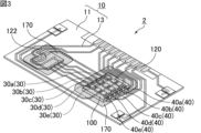
図2は、本発明の伸縮性実装基板の一例を模式的に示す斜視図である。
図2に示すように、伸縮性実装基板1は、伸縮性配線基板10と、モジュール100とを備える。
FIG. 2 is a perspective view schematically showing an example of the stretchable mounting board of the present invention.
As shown in FIG. 2, the
伸縮性配線基板10は、伸縮性基材11と、伸縮性基材11上に配置された伸縮性配線13とを備える。
The
伸縮性基材11は、例えば、伸縮性を有する樹脂材料から構成される。樹脂材料としては、例えば、熱可塑性ポリウレタン等が挙げられる。
The
伸縮性基材11の厚みは特に限定されないが、生体に貼り付けた際に生体表面の伸縮を阻害しない観点からは、100μm以下であることが好ましく、1μm以下であることがより好ましい。また、伸縮性基材11の厚みは、0.1μm以上であることが好ましい。
The thickness of the
伸縮性配線13は、導電性粒子と樹脂を含んでいることが好ましい。例えば、導電性粒子としてのAg、Cu、Niなどの金属粉と、シリコーン樹脂などのエラストマー系樹脂からなる混合物が挙げられる。
導電性粒子の平均粒径は特に限定されるものではないが、0.01μm以上、10μm以下であることが好ましい。
Preferably, the
Although the average particle size of the conductive particles is not particularly limited, it is preferably 0.01 μm or more and 10 μm or less.
伸縮性配線13の厚みは特に限定されないが、100μm以下であることが好ましく、50μm以下であることがより好ましい。また、伸縮性配線の厚みは0.01μm以上であることが好ましい。
The thickness of the
伸縮性配線13の線幅は特に限定されないが、0.1μm以上であることが好ましく、10mm以下であることがより好ましい。なお、伸縮性配線13の最小線幅とは、伸縮性基材11上に配置された伸縮性配線13のうち、線幅が最も短い部分の線幅を指す。
Although the line width of the
本発明の伸縮性実装基板において、伸縮性配線は、伸縮性基材上で交差していないことが好ましい。例えば、図2に示す伸縮性実装基板1において、伸縮性配線13は、伸縮性基材11上で交差していない。
In the stretchable mounting board of the present invention, it is preferable that the stretchable wiring does not intersect on the stretchable base material. For example, in the
伸縮性実装基板においては、伸縮性基材に搭載される電子部品の数が増加する程、回路が複雑化する。回路が複雑化すると、伸縮性配線同士を伸縮性基材上で交差させたクロス配線を形成する必要が生じやすい。しかしながら、クロス配線を形成すると、クロス配線を形成した領域における伸縮性実装基板の柔軟性が低下してしまうという問題が生じる。
また、クロス配線を形成するためには、製造工程を追加する必要が生じる。例えば、下層となる伸縮性配線の上に絶縁層を設け、その上にさらに伸縮性配線を設けるといった工程が必要となる。このような製造工程の複雑化は、製造コストの増加を招き好ましくない。
In a stretchable mounting board, the circuit becomes more complex as the number of electronic components mounted on the stretchable base material increases. When a circuit becomes complicated, it is likely to be necessary to form a cross wiring in which stretchable wires cross each other on a stretchable base material. However, when the cross wiring is formed, a problem arises in that the flexibility of the stretchable mounting board decreases in the region where the cross wiring is formed.
Further, in order to form cross wiring, it is necessary to add a manufacturing process. For example, it is necessary to provide a step of providing an insulating layer on top of the stretchable wiring that serves as the lower layer, and further providing a stretchable wire on top of the insulating layer. Such complication of the manufacturing process is undesirable because it increases manufacturing costs.
例えば、図1に示す伸縮性実装基板501では、Xで示す領域、及び、Yで示す領域において、合計3つのクロス配線が生じている。従って、伸縮性実装基板501を製造する際には、伸縮性基材511上に伸縮性配線513を形成する工程を設けた後、さらに、絶縁層を形成する工程、及び、上層となる伸縮性配線を形成する工程が必要となる。
伸縮性配線が伸縮性基材上で交差していないと、伸縮性実装基板にクロス配線を設けるための製造プロセスが必要なくなり、製造コストを低下させることができる。また、クロス配線が形成されることによって伸縮性配線基板の柔軟性が低下してしまうことを抑制できる。
For example, in the
If the stretchable wires do not cross each other on the stretchable base material, a manufacturing process for providing cross wires on the stretchable mounting board is not necessary, and manufacturing costs can be reduced. Further, it is possible to suppress the flexibility of the stretchable wiring board from being reduced due to the formation of cross wiring.
伸縮性配線基板10の表面には、後述する電子部品と電気的に接続するための電極30(30a、30b、30c、30d、30e)及び電極40(40a、40b、40c、40d、40e)が設けられている。
これらの電極は、伸縮性基材11上に配置された伸縮性配線13と接続されている。
On the surface of the
These electrodes are connected to
電極は、導電性粒子と樹脂を含んでいることが好ましい。導電性粒子及び樹脂としては、伸縮性配線13と同様のものを好適に用いることができる。
Preferably, the electrode contains conductive particles and resin. As the conductive particles and resin, those similar to those for the
伸縮性配線基板には、電子部品が実装されていてもよい。
例えば、図2に示す伸縮性配線基板10上には、電子部品120が実装されている。
Electronic components may be mounted on the stretchable wiring board.
For example, an
伸縮性配線基板に実装される電子部品は、生体データを取得する電子部品や、電磁波を照射する電子部品であることが好ましい。
生体データを取得する電子部品としては、例えば、加速度センサ、温度センサ、酸素飽和度センサ、水分センサ等が挙げられる。
生体に電磁波を照射する電子部品としては、コイル部品が挙げられる。
The electronic component mounted on the stretchable wiring board is preferably an electronic component that acquires biological data or an electronic component that irradiates electromagnetic waves.
Examples of electronic components that acquire biological data include acceleration sensors, temperature sensors, oxygen saturation sensors, moisture sensors, and the like.
An example of an electronic component that irradiates a living body with electromagnetic waves is a coil component.
伸縮性配線基板に実装される電子部品は、封止樹脂等で覆われていてもよい。
電子部品が封止樹脂で覆われていると、電子部品が水分の影響により電子部品の特性が低下することを防ぐことができる。
The electronic components mounted on the stretchable wiring board may be covered with a sealing resin or the like.
When the electronic component is covered with a sealing resin, it is possible to prevent the characteristics of the electronic component from deteriorating due to the influence of moisture.
図3は、本発明の伸縮性実装基板の別の一例を模式的に示す斜視図である。
図3に示す伸縮性実装基板2は、伸縮性実装基板10上に実装された電子部品及びモジュールが封止樹脂170で封止されている以外は、図2に示す伸縮性実装基板1と同様である。
図3に示す伸縮性実装基板2では、伸縮性配線基板10上に実装された電子部品122が、封止樹脂170で封止されている。
FIG. 3 is a perspective view schematically showing another example of the stretchable mounting board of the present invention.
The
In the
伸縮性配線基板に実装されるモジュールは、封止樹脂等で覆われていてもよい。
モジュールが封止樹脂で覆われていると、モジュール及びモジュールに実装された電子部品の特性が、水分の影響により低下することを防ぐことができる。
図3に示す伸縮性実装基板2では、伸縮性配線基板10上に実装されるモジュール100が、封止樹脂170で覆われている。
The module mounted on the stretchable wiring board may be covered with a sealing resin or the like.
When the module is covered with a sealing resin, the characteristics of the module and the electronic components mounted on the module can be prevented from deteriorating due to the influence of moisture.
In the
従来の伸縮性配線基板に実装される電子部品を封止樹脂で覆う場合には、例えば以下のような問題が生じていた。
封止樹脂は製造工程上の誤差などを考慮して、通常、電子部品よりも大きい領域を覆うように形成される。しかしながら、封止樹脂は伸縮性基材のような柔軟性を持たない。そのため、電子部品の数が増加するほど、伸縮性基板の表面を覆う樹脂の割合が増加し、伸縮性基板の柔軟性が低下してしまうという問題が生じやすい。この問題は、電子部品を覆う封止樹脂同士が接触してしまう程度に電子部品の実装密度が高まった際に、特に顕著となる。
すなわち、電子部品を封止樹脂で封止する場合には、電子部品の実装密度が高ければ高いほど、伸縮性基板の柔軟性を低下させてしまうという課題があった。
When covering electronic components mounted on a conventional stretchable wiring board with a sealing resin, the following problems have occurred, for example.
The sealing resin is usually formed to cover a larger area than the electronic component, taking into account errors in the manufacturing process. However, the sealing resin does not have flexibility like the stretchable base material. Therefore, as the number of electronic components increases, the proportion of resin covering the surface of the stretchable substrate increases, which tends to cause the problem that the flexibility of the stretchable substrate decreases. This problem becomes particularly noticeable when the packaging density of electronic components increases to the extent that the sealing resins that cover the electronic components come into contact with each other.
That is, when electronic components are sealed with a sealing resin, there is a problem in that the higher the mounting density of the electronic components, the lower the flexibility of the stretchable substrate.
これに対して、本発明の伸縮性配線基板は、モジュールを用いることで伸縮性配線基板に直接実装される電子部品の数を減らすことができるため、モジュールを封止樹脂で覆うことにより、電子部品を水分の影響から保護しつつ、電子部品の実装密度の向上と、伸縮性配線基板の柔軟性の低下の抑制を両立させることができる。 On the other hand, the stretchable wiring board of the present invention uses modules to reduce the number of electronic components that are directly mounted on the stretchable wiring board. While protecting the components from the influence of moisture, it is possible to simultaneously improve the mounting density of electronic components and suppress a decrease in flexibility of the stretchable wiring board.
封止樹脂としては、エポキシ樹脂、アクリル樹脂、シリコーン樹脂等が挙げられる。 Examples of the sealing resin include epoxy resin, acrylic resin, and silicone resin.
本発明の伸縮性実装基板は、平坦部を有していることが好ましい。
例えば、図2に示す伸縮性実装基板1では、電子部品122の上面が平坦となっている。従って、伸縮性実装基板1は平坦部を有しているといえる。伸縮性実装基板が平坦部を有していると、伸縮性実装基板を取り扱う場合に、実装機等を使用した際の吸着用部位として利用できる。
The stretchable mounting board of the present invention preferably has a flat portion.
For example, in the
なお、伸縮性配線基板に実装される電子部品やモジュールを封止樹脂で覆った場合も、封止樹脂の上面が平坦であれば、実装機などを使用した際の吸着用部位として使用できる平坦部となる。
例えば、図3に示す伸縮性実装基板2では、モジュール100を封止する封止樹脂170の上面、及び、電子部品122を封止する封止樹脂170の上面が平坦となっている。従って、伸縮性実装基板2は平坦部を有しているといえる。
Note that even when electronic components or modules mounted on a stretchable wiring board are covered with a sealing resin, if the top surface of the sealing resin is flat, the flat surface can be used as a suction part when using a mounting machine, etc. Becomes a department.
For example, in the
図4は、図2及び図3に示すモジュールの斜視図である。
図4に示すモジュール100は、多層基板110と、多層基板110の主面に実装された複数の電子部品120と、多層基板110の主面に設けられた複数の第1電極130(130a、130b、130c、130d、130e)及び第2電極140(140a、140b、140c、140d、140e)と、第1電極と第2電極とを多層基板の内部で電気的に接続する内部配線と、を備える。
なお、図4に示すモジュール100において、多層基板110の主面に実装される電子部品120の数は9個である。
FIG. 4 is a perspective view of the module shown in FIGS. 2 and 3.
The
Note that in the
複数の第1電極130(130a、130b、130c、130d、130e)が集中して配置される領域(図4中、破線で示す領域A1)が、第1電極配置領域A1である。
複数の第2電極140(140a、140b、140c、140d、140e)が集中して配置される領域(図4中、破線で示す領域B1)が、第2電極配置領域B1である。
The region where the plurality of first electrodes 130 (130a, 130b, 130c, 130d, 130e) are arranged in a concentrated manner (region A 1 indicated by a broken line in FIG. 4) is the first electrode arrangement region A 1 .
The region where the plurality of second electrodes 140 (140a, 140b, 140c, 140d, 140e) are arranged in a concentrated manner (region B 1 indicated by the broken line in FIG. 4) is the second electrode arrangement region B 1 .
第1電極配置領域A1に配置される第1電極と第2電極配置領域B1に配置される第2電極のうち、内部配線により接続されている2つの電極は、ノード電極ペアを構成する電極である。ノード電極ペアについては後述する。 Among the first electrode arranged in the first electrode arrangement area A 1 and the second electrode arranged in the second electrode arrangement area B 1 , the two electrodes connected by internal wiring constitute a node electrode pair. It is an electrode. The node electrode pair will be described later.
第1電極配置領域A1は、モジュールを平面視した際の一辺100aに位置しており、第2電極配置領域B1は、第1電極配置領域A1が配置されている辺100aと対向する辺100bに位置している。第1電極配置領域A1と第2電極配置領域B1とが、モジュールの対向する辺にそれぞれ位置していると、第1電極配置領域A1に配置される電極と第2電極配置領域B1に配置される電極との最短距離を長くすることができる。
The first electrode placement area A1 is located on one
従って、本発明の伸縮性実装基板においては、第1電極配置領域は、モジュールを平面視した際の一辺に位置しており、第2電極配置領域は、第1電極配置領域が配置されている辺と対向する辺に位置していることが好ましい。 Therefore, in the stretchable mounting board of the present invention, the first electrode placement area is located on one side when the module is viewed from above, and the second electrode placement area is located on one side where the first electrode placement area is placed. It is preferable that it is located on the side opposite to the side.
モジュールには、複数の電子部品が実装されている。
多層基板に実装される電子部品としては、増幅器(オペアンプ、トランジスタ等)、チップコンデンサ、チップ抵抗等が挙げられる。電子部品を実装する際の形態は特に限定されず、ベアチップ、ボールグリッドアレイ(BGA)、チップスケールパッケージ(CSP)、表面実装部品(SMD)等として実装されてもよい。
A plurality of electronic components are mounted on the module.
Examples of electronic components mounted on the multilayer board include amplifiers (operational amplifiers, transistors, etc.), chip capacitors, chip resistors, and the like. The form in which electronic components are mounted is not particularly limited, and may be mounted as a bare chip, ball grid array (BGA), chip scale package (CSP), surface mount device (SMD), or the like.
本発明の伸縮性実装基板は、複数の電子部品が実装されたモジュールを備えるため、伸縮性配線基板上に直接実装される電子部品の数を減らすことができる。 Since the stretchable mounting board of the present invention includes a module in which a plurality of electronic components are mounted, the number of electronic components directly mounted on the stretchable wiring board can be reduced.
モジュールを構成する多層基板は、絶縁層が複数積層されてなる。 The multilayer substrate that constitutes the module is made up of a plurality of laminated insulating layers.
多層基板の絶縁層の積層数は、特に限定されないが、4層以上であることが好ましい。 The number of laminated insulating layers of the multilayer substrate is not particularly limited, but is preferably four or more layers.
本発明の伸縮性実装基板において、モジュールを構成する多層基板の絶縁層の積層数は、伸縮性配線基板を構成する伸縮性基材の積層数よりも多いことが好ましい。 In the stretchable mounting board of the present invention, it is preferable that the number of laminated insulating layers of the multilayer board constituting the module is greater than the number of laminated layers of the stretchable base material constituting the stretchable wiring board.
絶縁層を構成する材料としては、フェノール樹脂、エポキシ樹脂、ポリイミド樹脂、ビスマレイミドトリアジン樹脂、フッ素樹脂、ポリフェニレンオキサイド樹脂等の樹脂や、低温焼結セラミック材料等が挙げられる。 Examples of the material constituting the insulating layer include resins such as phenol resin, epoxy resin, polyimide resin, bismaleimide triazine resin, fluororesin, and polyphenylene oxide resin, and low-temperature sintered ceramic materials.
絶縁層を構成する上記樹脂は、紙やガラス繊維からなる基材に含浸されていてもよい。 The resin constituting the insulating layer may be impregnated into a base material made of paper or glass fiber.
低温焼結セラミック材料とは、セラミック材料のうち、1000℃以下の焼成温度で焼結可能であり、内部配線となる金属材料として好ましく使用される銀や銅との同時焼成が可能である材料を意味する。
低温焼結セラミック材料としては、SiO2-CaO-Al2O3-B2O3系ガラスセラミック又はSiO2-MgO-Al2O3-B2O3系ガラスセラミックを含むことが好ましい。
Low-temperature sintered ceramic materials refer to ceramic materials that can be sintered at a firing temperature of 1000°C or less, and that can be fired simultaneously with silver and copper, which are preferably used as metal materials for internal wiring. means.
The low-temperature sintered ceramic material preferably includes a SiO 2 --CaO--Al 2 O 3 --B 2 O 3 -based glass ceramic or a SiO 2 --MgO--Al 2 O 3 --B 2 O 3 -based glass ceramic.
多層基板は、内部配線を備える。
内部配線は、多層基板の主面に設けられた複数の電極を、多層基板の内部で電気的に接続する。
The multilayer board includes internal wiring.
The internal wiring electrically connects a plurality of electrodes provided on the main surface of the multilayer substrate inside the multilayer substrate.
内部配線は、多層基板に設けられた第1電極と第2電極とを接続していてもよいし、多層基板に設けられた第1電極又は第2電極と多層基板に実装された電子部品とを接続していてもよいし、多層基板に実装された複数の電子部品同士を接続していてもよい。 The internal wiring may connect a first electrode and a second electrode provided on the multilayer board, or may connect the first electrode or the second electrode provided on the multilayer board and an electronic component mounted on the multilayer board. or a plurality of electronic components mounted on a multilayer board may be connected to each other.
内部配線を構成する材料としては、銅、銀、錫、ニッケル、金及びこれらの合金等が挙げられる。 Examples of materials constituting the internal wiring include copper, silver, tin, nickel, gold, and alloys thereof.
モジュールの内部に設けられる内部配線の一例について、図5を参照しながら説明する。 An example of internal wiring provided inside the module will be described with reference to FIG. 5.
図5は、図2及び図3に示す伸縮性実装基板のモジュールが実装されている領域を拡大した透過上面図である。
図5では、電極30(30a、30b、30c、30d、30e)及び電極40(40a、40b、40c、40d、40e)が設けられた伸縮性配線基板上に、図4に示すモジュールが実装されている。
図5中、二点鎖線で示す矩形形状が、伸縮性配線基板10上に実装されるモジュール100の位置を示している。
FIG. 5 is an enlarged transparent top view of the region of the stretchable mounting board shown in FIGS. 2 and 3 where modules are mounted.
In FIG. 5, the module shown in FIG. 4 is mounted on a stretchable wiring board on which electrodes 30 (30a, 30b, 30c, 30d, 30e) and electrodes 40 (40a, 40b, 40c, 40d, 40e) are provided. ing.
In FIG. 5, a rectangular shape indicated by a two-dot chain line indicates the position of the
図5では、図4に示すモジュール100の第1電極130(130a、130b、130c、130d、130e)及び第2電極140(140a、140b、140c、140d、140e)が、平面視において、それぞれ、伸縮性配線基板上に設けられた電極30(30a、30b、30c、30d、30e)及び電極40(40a、40b、40c、40d、40e)と重なるように配置されている。従って、モジュール100と伸縮性配線基板とは、電極を介して電気的に接続されているといえる。
In FIG. 5, the first electrodes 130 (130a, 130b, 130c, 130d, 130e) and the second electrodes 140 (140a, 140b, 140c, 140d, 140e) of the
図5に示すように、モジュール100を構成する多層基板110は、内部配線150a及び内部配線150bを有する。
As shown in FIG. 5, the
本発明の伸縮性実装基板では、本来伸縮性基材上に配置される伸縮性配線の一部を、モジュール内の内部配線として実装しているといえる。伸縮性基材上に配置される伸縮性配線の一部を、モジュール中に配置される内部配線に置き換える事によって、必要な伸縮性基材の面積を減らすことができる。従って、伸縮性基材の面積を減らすことで、伸縮性実装基板を小型化及び低コスト化できる。 In the stretchable mounting board of the present invention, it can be said that a part of the stretchable wiring originally placed on the stretchable base material is mounted as internal wiring within the module. By replacing a portion of the stretchable wiring disposed on the stretchable base material with internal wiring disposed in the module, the required area of the stretchable base material can be reduced. Therefore, by reducing the area of the stretchable base material, the stretchable mounting board can be made smaller and lower in cost.
内部配線150aは、第1電極130aと第2電極140dとを電気的に接続している。内部配線150aにより接続された第1電極130aと第2電極140dは同じ電位となる。
内部配線150bは、第1電極130bと第2電極140aとを電気的に接続している。内部配線150bにより接続された第1電極130bと第2電極140aは同じ電位となる。
本明細書では、内部配線を通じて同じ電位となる2つの第1電極と第2電極のペアをノード電極ペアともいう。すなわち、第1電極130aと第2電極140dはノード電極ペアであり、第1電極130bと第2電極140aはノード電極ペアである。
図5に示すように、モジュール100は、ノード電極ペアを2組有する。
In this specification, a pair of two first and second electrodes that have the same potential through internal wiring is also referred to as a node electrode pair. That is, the
As shown in FIG. 5, the
ノード電極ペアを構成する2つの電極(第1電極130aと第2電極140d、及び、第1電極130bと第2電極140a)は、第1電極配置領域A1及び第2電極配置領域B1に分かれて設けられている。換言すると、ノード電極ペアを構成する2つの電極は、同じ電極配置領域に配置されない。
The two electrodes (
本発明の伸縮性実装基板においては、ノード電極ペアを構成している内部配線と、伸縮性基材上に配置された伸縮性配線とが、伸縮性実装基板を平面視した際に交差している。
例えば、図5に示す伸縮性実装基板1では、内部配線150a及び内部配線150bが、電極30dに接続される伸縮性配線13並びに電極40c及び40eに接続される伸縮性配線13と、それぞれ交差している。
In the stretchable mounting board of the present invention, the internal wiring constituting the node electrode pair and the stretchable wiring arranged on the stretchable base material intersect with each other when the stretchable mounting board is viewed from above. There is.
For example, in the
上述した内部配線の構成は、モジュール内に形成された内部配線ではなく伸縮性配線を用いた場合に、伸縮性配線同士が交差してしまう例であるといえる。従って、本発明の伸縮性実装基板は、伸縮性基材上にクロス配線が形成されるような伸縮性配線の配置を回避できる構成を備えているといえる。従って、クロス配線の形成に伴う伸縮性実装基板の柔軟性の低下、及び、製造コストの増加を抑制することができる。 The configuration of the internal wiring described above can be said to be an example in which when stretchable wires are used instead of internal wires formed in the module, the stretchable wires cross each other. Therefore, it can be said that the stretchable mounting board of the present invention has a configuration that can avoid arrangement of stretchable wiring such that cross wiring is formed on the stretchable base material. Therefore, it is possible to suppress a decrease in the flexibility of the stretchable mounting board and an increase in manufacturing costs due to the formation of cross wiring.
本発明の伸縮性実装基板においては、モジュールを平面視した際に、ノード電極のペアを構成する内部配線同士が、多層基板の内部において、平面視において交差していることが好ましい。
例えば、図5では、ノード電極ペアを構成する内部配線150aと、別のノード電極ペアを構成する内部配線150bとは、モジュール100を平面視した際に交差している。
なお、内部配線150aと内部配線150bは、多層基板の異なる層に位置している。従って、平面視において内部配線150aと内部配線150bが交差していたとしても、内部配線150aと内部配線150bは電気的に接触していない。
In the stretchable mounting board of the present invention, when the module is viewed in plan, it is preferable that the internal wirings forming the pair of node electrodes intersect with each other in plan view inside the multilayer board.
For example, in FIG. 5, an
Note that the
モジュール100中に設けられた内部配線150a及び内部配線150bの線幅(図5中、両矢印w1で示す長さ)は、伸縮性配線13の最小線幅(図5中、両矢印w2で示す長さ)よりも短い。
The line width of the
すなわち、本発明の伸縮性実装基板において、内部配線の最小線幅は、伸縮性配線の最小線幅よりも短いことが好ましい。内部配線の最小線幅が、伸縮性配線の最小線幅よりも短いと、モジュールの配線密度を、伸縮性基板の配線密度よりも高くすることができるため、伸縮性実装基板の小型化に寄与する。 That is, in the stretchable mounting board of the present invention, the minimum line width of the internal wiring is preferably shorter than the minimum line width of the stretchable wiring. If the minimum line width of the internal wiring is shorter than the minimum line width of the stretchable wiring, the wiring density of the module can be higher than that of the stretchable board, which contributes to the miniaturization of the stretchable mounting board. do.
内部配線の最小線幅は特に限定されないが、例えば100μm以下であることが好ましい。 Although the minimum line width of the internal wiring is not particularly limited, it is preferably 100 μm or less, for example.
第1電極配置領域A1に配置される第1電極と、第2電極配置領域B1に配置される第2電極との間の最短距離は、両矢印L1で示される長さである。この長さL1は、伸縮性基材11上に配置される伸縮性配線13の最小線幅w2よりも長いことが好ましい。
すなわち、ノード電極ペアを構成する第1電極と第2電極との間の最短距離が、伸縮性配線の最小線幅よりも長いことが好ましい。
長さL1が長さw2よりも長いと、第1電極配置領域A1に配置された第1電極と第2電極配置領域B1に配置された第2電極との間に、伸縮性配線13を通過させることができる隙間が存在しているといえる。そのため、伸縮性配線基板10とモジュール100との間に、平面視においてモジュール100を横切るような伸縮性配線13を設けることが可能となる。
The shortest distance between the first electrode placed in the first electrode placement area A1 and the second electrode placed in the second electrode placement area B1 is the length shown by the double-headed arrow L1 . This length L 1 is preferably longer than the minimum line width w 2 of the
That is, it is preferable that the shortest distance between the first electrode and the second electrode constituting the node electrode pair is longer than the minimum line width of the stretchable wiring.
When the length L1 is longer than the length W2 , there is a stretchable area between the first electrode placed in the first electrode placement area A1 and the second electrode placed in the second electrode placement area B1 . It can be said that there is a gap through which the
伸縮性配線の最小間隔とは、2本の伸縮性配線を平行に配置するときに、互いに干渉しないようにパターン形成ができる最小の間隔である。伸縮性配線の最小間隔は、伸縮性配線を構成する材料、伸縮性基材を構成する材料、及び、伸縮性実装基板と接続される電源の電圧等により適宜決定される。
伸縮性配線の最小間隔は、例えば、300μm以下であることが好ましく、200μm以下であることがより好ましい。
The minimum interval between stretchable wirings is the minimum interval at which a pattern can be formed without interfering with each other when two stretchable wirings are arranged in parallel. The minimum interval between the stretchable wirings is appropriately determined based on the material forming the stretchable wiring, the material forming the stretchable base material, the voltage of the power supply connected to the stretchable mounting board, and the like.
For example, the minimum interval between the stretchable wirings is preferably 300 μm or less, and more preferably 200 μm or less.
上記長さL1は、伸縮性配線の最小線幅と伸縮性配線の最小間隔の2倍値の合計よりも大きいことが好ましい。
長さL1が、伸縮性配線の最小線幅と伸縮性配線の最小間隔の2倍値の合計よりも大きいと、伸縮性配線基板とモジュールとの間に、電極間の長さL1を2等分する点を通る最小線幅の1本の伸縮性配線を、電極と干渉しないように配置したパターンを形成することができる。
The length L1 is preferably larger than the sum of the minimum line width of the stretchable wiring and twice the minimum interval between the stretchable wirings.
If the length L1 is larger than the sum of the minimum line width of the stretchable wiring and twice the minimum interval of the stretchable wiring, the length L1 between the electrodes is set between the stretchable wiring board and the module. It is possible to form a pattern in which one stretchable wire with the minimum line width passing through the bisecting points is arranged so as not to interfere with the electrodes.
すなわち、本発明の伸縮性実装基板においては、ノード電極ペアを構成する第1電極と第2電極との間の最短距離が、伸縮性配線の最小線幅と伸縮性配線の最小間隔の2倍値の合計よりも大きいことが好ましい。 That is, in the stretchable mounting board of the present invention, the shortest distance between the first electrode and the second electrode constituting the node electrode pair is twice the minimum line width of the stretchable wiring and the minimum distance between the stretchable wiring. It is preferably greater than the sum of the values.
上記長さL1は、伸縮性配線の最小線幅の2倍値と、伸縮性配線の最小間隔の3倍値の合計よりも大きいことが好ましい。
長さL1が、伸縮性配線の最小線幅の2倍値と、伸縮性配線の最小間隔の3倍値の合計よりも大きいと、伸縮性配線基板とモジュールとの間に、電極間の長さL1を3等分する2点をそれぞれ通る最小線幅の2本の伸縮性配線を、隣接する電極及び隣接する伸縮性配線と干渉しないように配置したパターンを形成することができる。
The length L1 is preferably larger than the sum of twice the minimum line width of the stretchable wiring and triple the minimum interval between the stretchable wires.
If the length L1 is larger than the sum of twice the minimum line width of the stretchable wiring and triple the minimum spacing of the stretchable wiring, there is a gap between the electrodes between the stretchable wiring board and the module. A pattern can be formed in which two stretchable wires each having a minimum line width passing through two points that divide the length L1 into three are arranged so as not to interfere with adjacent electrodes and adjacent stretchable wires.
上記長さL1は、伸縮性配線の最小線幅の3倍値と、伸縮性配線の最小間隔の4倍値の合計よりも大きいことが好ましい。
長さL1が、伸縮性配線の最小線幅の3倍値と、伸縮性配線の最小間隔の4倍値の合計よりも大きいと、伸縮性配線基板とモジュールとの間に、電極間の長さL1を4等分する3点をそれぞれ通る最小線幅の3本の伸縮性配線を、隣接する電極及び/又は隣接する伸縮性配線と干渉しないように配置したパターンを形成することができる。
The length L1 is preferably larger than the sum of three times the minimum line width of the stretchable wiring and four times the minimum interval between the stretchable wires.
If the length L1 is larger than the sum of three times the minimum line width of the stretchable wiring and four times the minimum interval of the stretchable wiring, there will be a gap between the electrodes between the stretchable wiring board and the module. It is possible to form a pattern in which three stretchable wires with the minimum line width passing through three points that divide the length L1 into four are arranged so as not to interfere with adjacent electrodes and/or adjacent stretchable wires. can.
なお、図2、図3、図4及び図5に示すモジュール100では、すべての電極(第1電極130及び第2電極140)がモジュール100の辺100a及び辺100bに配置されているが、本発明の伸縮性実装基板においては、モジュールの辺から離れた位置に電極が配置されていてもよい。
Note that in the
モジュールの辺から離れた位置に電極が配置されている例について、図6を参照しながら説明する。 An example in which electrodes are arranged at positions away from the sides of the module will be described with reference to FIG. 6.
図6は、本発明の伸縮性実装基板を構成するモジュールの別の一例を模式的に示す斜視図である。 FIG. 6 is a perspective view schematically showing another example of a module constituting the stretchable mounting board of the present invention.
図6に示すモジュール102は、図4に示したモジュール100の電子部品が実装されていない主面に、さらに電極130f、130g、140f、140gを設けたものに相当する。すなわち、図6に示すモジュール102は、図4に示すモジュール100とは表裏が逆となっている。
電極130f、電極130g、電極140f及び電極140gはいずれも、モジュールの辺から離れた位置に設けられた電極である。
The
The
ここで、モジュールに設けられた電極が、第1電極配置領域と第2電極配置領域のどちらに帰属するかを決定する際、当該電極がノード電極ペアを構成している場合には、内部配線により接続される対となる電極が配置されている電極配置領域とは別の電極配置領域に帰属するものとする。一方、モジュールに設けられた電極がノード電極ペアを構成する電極ではない場合には、平面視において最も近い位置に配置されている電極が配置されている電極配置領域に帰属するものとする。 Here, when determining whether an electrode provided in a module belongs to the first electrode placement area or the second electrode placement area, if the electrode constitutes a node electrode pair, internal wiring It belongs to an electrode arrangement area different from the electrode arrangement area where the pair of electrodes connected by is arranged. On the other hand, if the electrodes provided on the module are not electrodes constituting a node electrode pair, the electrodes are assumed to belong to the electrode placement area where the electrode placed closest in plan view is placed.
まず、図4に示すモジュール100と同様に、電極130a、130b、130c、130d及び130eは、第1電極配置領域A2に帰属する。また、電極140a、140b、140c、140d及び140eは、第2電極配置領域B2に帰属する。すなわち、電極130a、130b、130c、130d及び130eは第1電極であり、電極140a、140b、140c、140d及び140eは第2電極である。
First, like the
平面視において、電極130fに最も近い位置に配置されている電極は、第1電極130bである。第1電極130bは、第1電極配置領域A2に帰属する電極であるから、電極130fも第1電極配置領域A2に帰属する。すなわち、電極130fは第1電極である。
In plan view, the electrode located closest to the
平面視において、電極130gに最も近い位置に配置されている電極は、第1電極130dである。第1電極130dは、第1電極配置領域A2に帰属する電極であるから、電極130gも、第1電極配置領域A2に帰属する。すなわち、電極130gは第1電極である。
In plan view, the electrode located closest to the
平面視において、電極140fに最も近い位置に配置されている電極は、第2電極140bである。第2電極140bは、第2電極配置領域B2に帰属する電極であるから、電極140fも、第2電極配置領域B2に帰属する。すなわち、電極140fは第2電極である。
In plan view, the electrode located closest to the
平面視において、電極140gに最も近い位置に配置されている電極は、第2電極140dである。第2電極140dは、第2電極配置領域B2に帰属する電極であるから、電極140gも、第2電極配置領域B2に帰属する。すなわち、電極140gは第2電極である。
In plan view, the electrode located closest to the
従って、図6に示すモジュール102では、第1電極配置領域A2に、7つの第1電極(第1電極130a、130b、130c、130d、130e、130f、130g)が配置されている。また、第2電極配置領域B2に、7つの第2電極(第2電極140a、140b、140c、140d、140e、140f、140g)が配置されている。
Therefore, in the
図7は、図6に示すモジュールを伸縮性配線基板に実装した状態の一例を模式的に示す透過上面図である。なお、図7では、伸縮性実装基板上に設けられた伸縮性配線のうち、モジュールを構成する電極と電気的に接続されない伸縮性配線のみを図示し、その他の伸縮性配線を省略している。 FIG. 7 is a transparent top view schematically showing an example of a state in which the module shown in FIG. 6 is mounted on a stretchable wiring board. In addition, in FIG. 7, among the stretchable wiring provided on the stretchable mounting board, only the stretchable wiring that is not electrically connected to the electrodes constituting the module is illustrated, and the other stretchable wiring is omitted. .
図7では、電極30(30a、30b、30c、30d、30e、30f、30g)及び電極40(40a、40b、40c、40d、40e、40f、40g)が設けられた伸縮性配線基板上に、図6に示すモジュールが実装されている。
図7中、二点鎖線で示す矩形形状が、伸縮性配線基板上に実装されるモジュール102の位置を示している。
In FIG. 7, on a stretchable wiring board on which electrodes 30 (30a, 30b, 30c, 30d, 30e, 30f, 30g) and electrodes 40 (40a, 40b, 40c, 40d, 40e, 40f, 40g) are provided, The module shown in FIG. 6 is implemented.
In FIG. 7, a rectangular shape indicated by a two-dot chain line indicates the position of the
図7では、図6に示すモジュール102の第1電極130(130a、130b、130c、130d、130e、130f、130g)及び第2電極140(140a、140b、140c、140d、140e、140f、140g)が、平面視において、それぞれ、伸縮性配線基板上に設けられた電極30(30a、30b、30c、30d、30e、30f、30g)及び電極40(40a、40b、40c、40d、40e、40f、40g)と重なるように配置されている。従って、モジュール102と伸縮性実装基板とは、電極を介して電気的に接続されているといえる。
In FIG. 7, the first electrode 130 (130a, 130b, 130c, 130d, 130e, 130f, 130g) and the second electrode 140 (140a, 140b, 140c, 140d, 140e, 140f, 140g) of the
図7に示すように、モジュール102を構成する多層基板は、内部配線150c及び150dを有する。
内部配線150cは、第1電極130fと第2電極140gとを電気的に接続している。内部配線150cにより接続された第1電極130fと第2電極140gは同じ電位となる。
内部配線150dは、第1電極130gと第2電極140fとを電気的に接続している。内部配線150dにより接続された第1電極130gと第2電極140fは同じ電位となる。
従って、第1電極130fと第2電極140gはノード電極ペアであり、第1電極130gと第2電極140fはノード電極ペアである。
図7に示すように、モジュール102はノード電極ペアを2組有する。
As shown in FIG. 7, the multilayer
The
The
Therefore, the
As shown in FIG. 7,
図7には、モジュール102を図面縦方向に横切る伸縮性配線13を示している。第1電極配置領域A2に配置された第1電極と第2電極配置領域B2に配置された第2電極との間の最短距離(図7中、両矢印L2で示される長さ)は、伸縮性配線13の最小線幅w2よりも長くなっている。そのため、伸縮性配線基板10とモジュール102との間に、平面視においてモジュール102を横切るような伸縮性配線13を設けることが可能となる。
FIG. 7 shows the
本発明の伸縮性実装基板に用いられるモジュールは、多層基板の両方の主面に電子部品が実装された両面実装モジュールであってもよい。モジュールが両面実装モジュールであると、同一面積に実装可能な電子部品及び配線数を増加させることができるため、モジュールを小型化することができる。 The module used in the stretchable mounting board of the present invention may be a double-sided mounting module in which electronic components are mounted on both main surfaces of a multilayer board. If the module is a double-sided mounting module, the number of electronic components and wiring that can be mounted in the same area can be increased, so the module can be made smaller.
図8は両面実装モジュールの一例を模式的に示す断面図である。
図8に示す両面実装モジュール200では、多層基板210の一方主面210aに電子部品220a、電子部品220b及び電子部品220cが実装され、一方主面210aと反対側の主面である他方主面210bに電子部品220dが実装されている。
他方主面210bには、電子部品220dの他に端子230が備えられており、端子230が伸縮性配線基板10上の電極40と電気的に接続されることで、伸縮性配線基板10上に実装される。
両面実装モジュール200は、封止樹脂170により封止されている。
FIG. 8 is a cross-sectional view schematically showing an example of a double-sided mounting module.
In the double-
The other
The double-
本発明の伸縮性実装基板は、例えば、伸縮性配線基板を準備する工程と、モジュールを準備する工程と、伸縮性配線基板にモジュールを実装する工程と、により得ることができる。 The stretchable mounting board of the present invention can be obtained, for example, by the steps of preparing a stretchable wiring board, preparing a module, and mounting the module on the stretchable wiring board.
1、2 伸縮性実装基板
10 伸縮性配線基板
11 伸縮性基材
13 伸縮性配線
30、30a、30b、30c、30d、30e、30f、30g 伸縮性配線基板上の電極
40、40a、40b、40c、40d、40e、40f、40g 伸縮性配線基板上の電極
100、102 モジュール
100a、100b モジュールを平面視した際の辺
110 多層基板
120、120a、120b、122 電子部品
130、130a、130b、130c、130d、130e、130f、130g 第1電極
140、140a、140b、140c、140d、140e、140f、140g 第2電極
150a、150b、150c、150d 内部配線
170 封止樹脂
200 両面実装モジュール
210 多層基板
210a 多層基板の一方主面
210b 多層基板の他方主面
220a、220b、220c、220d 電子部品
230 端子(外部電極)
501 伸縮性実装基板
511 伸縮性基材
513 伸縮性配線
520 電子部品
A1、A2 第1電極配置領域
B1、B2 第2電極配置領域
L1、L2 第1電極配置領域に配置された第1電極と第2電極配置領域に配置された第2電極の最短距離
w1 内部配線の線幅
w2 伸縮性配線の最小線幅
X、Y クロス配線が形成された領域
1, 2
501
Claims (10)
前記伸縮性配線基板は、伸縮性基材と、前記伸縮性基材上に配置された伸縮性配線とを備え、
前記モジュールは、多層基板と、前記多層基板の主面に実装された複数の電子部品と、前記多層基板の主面に設けられて、前記伸縮性配線基板に電気的に接続される複数の第1電極および第2電極と、前記第1電極と前記第2電極とを前記多層基板の内部で電気的に接続する内部配線と、を備え、
前記モジュールは、前記第1電極が複数個集中して配置される領域である第1電極配置領域、及び、前記第2電極が複数個集中して配置される領域である第2電極配置領域を有し、
前記モジュールは、内部配線と、前記内部配線によって電気的に接続された前記第1電極及び前記第2電極と、からなるノード電極ペアを有し、
前記ノード電極ペアを構成する前記内部配線と、前記伸縮性基材上に配置された前記伸縮性配線とが、前記伸縮性配線基板を平面視した際に交差しており、
前記内部配線は、金属配線であり、
前記伸縮性配線は、金属粉とエラストマー系樹脂からなる混合物である、ことを特徴とする伸縮性実装基板。 A stretchable mounting board comprising a stretchable wiring board and a module mounted on the surface of the stretchable wiring board,
The stretchable wiring board includes a stretchable base material and stretchable wiring arranged on the stretchable base material,
The module includes a multilayer substrate, a plurality of electronic components mounted on the main surface of the multilayer substrate, and a plurality of electronic components mounted on the main surface of the multilayer substrate and electrically connected to the stretchable wiring board. one electrode, a second electrode, and an internal wiring that electrically connects the first electrode and the second electrode inside the multilayer substrate,
The module includes a first electrode placement area where a plurality of the first electrodes are arranged in a concentrated manner, and a second electrode placement area where a plurality of the second electrodes are placed in a concentrated manner. have,
The module has a node electrode pair consisting of an internal wiring, and the first electrode and the second electrode electrically connected by the internal wiring,
The internal wiring constituting the node electrode pair and the stretchable wire arranged on the stretchable base material intersect when the stretchable wiring board is viewed from above,
The internal wiring is metal wiring,
A stretchable mounting board characterized in that the stretchable wiring is a mixture of metal powder and elastomer resin .
ノード電極ペアを構成する内部配線同士が、前記多層配線の内部において、平面視で交差している、請求項1~9のいずれかに記載の伸縮性実装基板。 having a plurality of the node electrode pairs,
10. The stretchable mounting board according to claim 1, wherein internal wirings constituting a pair of node electrodes intersect with each other in plan view inside the multilayer wiring.
Applications Claiming Priority (3)
| Application Number | Priority Date | Filing Date | Title |
|---|---|---|---|
| JP2021093823 | 2021-06-03 | ||
| JP2021093823 | 2021-06-03 | ||
| PCT/JP2022/014498 WO2022254908A1 (en) | 2021-06-03 | 2022-03-25 | Stretchable mounting substrate |
Publications (3)
| Publication Number | Publication Date |
|---|---|
| JPWO2022254908A1 JPWO2022254908A1 (en) | 2022-12-08 |
| JPWO2022254908A5 JPWO2022254908A5 (en) | 2023-05-15 |
| JP7450742B2 true JP7450742B2 (en) | 2024-03-15 |
Family
ID=84323048
Family Applications (1)
| Application Number | Title | Priority Date | Filing Date |
|---|---|---|---|
| JP2022551319A Active JP7450742B2 (en) | 2021-06-03 | 2022-03-25 | Stretchable mounting board |
Country Status (4)
| Country | Link |
|---|---|
| US (1) | US20230048568A1 (en) |
| JP (1) | JP7450742B2 (en) |
| CN (1) | CN219718608U (en) |
| WO (1) | WO2022254908A1 (en) |
Citations (3)
| Publication number | Priority date | Publication date | Assignee | Title |
|---|---|---|---|---|
| JP2004303944A (en) | 2003-03-31 | 2004-10-28 | Matsushita Electric Ind Co Ltd | Module substrate and its manufacturing method |
| JP2017147379A (en) | 2016-02-19 | 2017-08-24 | パナソニックIpマネジメント株式会社 | Surface mounting jumper board |
| JP2020174067A (en) | 2019-04-08 | 2020-10-22 | 大日本印刷株式会社 | Wiring board and manufacturing method thereof |
Family Cites Families (1)
| Publication number | Priority date | Publication date | Assignee | Title |
|---|---|---|---|---|
| JP3064751B2 (en) * | 1993-08-03 | 2000-07-12 | 太平洋セメント株式会社 | Method for manufacturing multilayer jumper chip |
-
2022
- 2022-03-25 JP JP2022551319A patent/JP7450742B2/en active Active
- 2022-03-25 WO PCT/JP2022/014498 patent/WO2022254908A1/en active Application Filing
- 2022-03-25 CN CN202290000156.8U patent/CN219718608U/en active Active
- 2022-11-01 US US17/978,357 patent/US20230048568A1/en active Pending
Patent Citations (3)
| Publication number | Priority date | Publication date | Assignee | Title |
|---|---|---|---|---|
| JP2004303944A (en) | 2003-03-31 | 2004-10-28 | Matsushita Electric Ind Co Ltd | Module substrate and its manufacturing method |
| JP2017147379A (en) | 2016-02-19 | 2017-08-24 | パナソニックIpマネジメント株式会社 | Surface mounting jumper board |
| JP2020174067A (en) | 2019-04-08 | 2020-10-22 | 大日本印刷株式会社 | Wiring board and manufacturing method thereof |
Also Published As
| Publication number | Publication date |
|---|---|
| CN219718608U (en) | 2023-09-19 |
| WO2022254908A1 (en) | 2022-12-08 |
| US20230048568A1 (en) | 2023-02-16 |
| JPWO2022254908A1 (en) | 2022-12-08 |
Similar Documents
| Publication | Publication Date | Title |
|---|---|---|
| KR100546374B1 (en) | Multi chip package having center pads and method for manufacturing the same | |
| US7968991B2 (en) | Stacked package module and board having exposed ends | |
| TWI520190B (en) | Memory card and sd card | |
| CN111627871A (en) | Semiconductor package | |
| JP3785083B2 (en) | Semiconductor device, electronic card and pad rearrangement substrate | |
| US10021791B2 (en) | Multilayer wiring substrate | |
| JP5611315B2 (en) | Package carrier | |
| JP2011066344A (en) | Semiconductor device and electronic device | |
| KR101391089B1 (en) | Semiconductor package and methods for fabricating the same | |
| JP7450742B2 (en) | Stretchable mounting board | |
| US11101206B2 (en) | Semiconductor device and electronic device | |
| KR20100095901A (en) | Stack type semiconductor package | |
| KR102578797B1 (en) | Semiconductor package | |
| US7135642B2 (en) | Integrated circuit carrier with conductive rings and semiconductor device integrated with the carrier | |
| JP3450477B2 (en) | Semiconductor device and manufacturing method thereof | |
| US20090284941A1 (en) | Semiconductor package, mounting circuit board, and mounting structure | |
| JP2005057271A (en) | Semiconductor chip package and stacked module having functional part and packaging part arranged horizontally on common plane | |
| JP2009177123A (en) | Stacked-chip package structure and manufacturing method thereof | |
| KR101480554B1 (en) | Pcb assembly | |
| US10881006B2 (en) | Package carrier and package structure | |
| TW201413878A (en) | Flexible printed circuit board and chip package structure | |
| KR102345061B1 (en) | Semiconductor package | |
| JP4640950B2 (en) | Semiconductor device | |
| JP2023165124A (en) | Semiconductor device | |
| US20110193204A1 (en) | Semiconductor device |
Legal Events
| Date | Code | Title | Description |
|---|---|---|---|
| A521 | Request for written amendment filed |
Free format text: JAPANESE INTERMEDIATE CODE: A523 Effective date: 20220825 |
|
| A621 | Written request for application examination |
Free format text: JAPANESE INTERMEDIATE CODE: A621 Effective date: 20220825 |
|
| A871 | Explanation of circumstances concerning accelerated examination |
Free format text: JAPANESE INTERMEDIATE CODE: A871 Effective date: 20220825 |
|
| A131 | Notification of reasons for refusal |
Free format text: JAPANESE INTERMEDIATE CODE: A131 Effective date: 20221018 |
|
| A521 | Request for written amendment filed |
Free format text: JAPANESE INTERMEDIATE CODE: A523 Effective date: 20221214 |
|
| A02 | Decision of refusal |
Free format text: JAPANESE INTERMEDIATE CODE: A02 Effective date: 20230307 |
|
| A521 | Request for written amendment filed |
Free format text: JAPANESE INTERMEDIATE CODE: A523 Effective date: 20230531 |
|
| A911 | Transfer to examiner for re-examination before appeal (zenchi) |
Free format text: JAPANESE INTERMEDIATE CODE: A911 Effective date: 20230608 |
|
| A912 | Re-examination (zenchi) completed and case transferred to appeal board |
Free format text: JAPANESE INTERMEDIATE CODE: A912 Effective date: 20230901 |
|
| A61 | First payment of annual fees (during grant procedure) |
Free format text: JAPANESE INTERMEDIATE CODE: A61 Effective date: 20240305 |
|
| R150 | Certificate of patent or registration of utility model |
Ref document number: 7450742 Country of ref document: JP Free format text: JAPANESE INTERMEDIATE CODE: R150 |