JP7446552B1 - Electric motor - Google Patents
Electric motor Download PDFInfo
- Publication number
- JP7446552B1 JP7446552B1 JP2023579130A JP2023579130A JP7446552B1 JP 7446552 B1 JP7446552 B1 JP 7446552B1 JP 2023579130 A JP2023579130 A JP 2023579130A JP 2023579130 A JP2023579130 A JP 2023579130A JP 7446552 B1 JP7446552 B1 JP 7446552B1
- Authority
- JP
- Japan
- Prior art keywords
- coil
- printed circuit
- circuit board
- armature
- coils
- Prior art date
- Legal status (The legal status is an assumption and is not a legal conclusion. Google has not performed a legal analysis and makes no representation as to the accuracy of the status listed.)
- Active
Links
Images


Classifications
-
- H—ELECTRICITY
- H02—GENERATION; CONVERSION OR DISTRIBUTION OF ELECTRIC POWER
- H02K—DYNAMO-ELECTRIC MACHINES
- H02K3/00—Details of windings
- H02K3/04—Windings characterised by the conductor shape, form or construction, e.g. with bar conductors
- H02K3/26—Windings characterised by the conductor shape, form or construction, e.g. with bar conductors consisting of printed conductors
-
- H—ELECTRICITY
- H02—GENERATION; CONVERSION OR DISTRIBUTION OF ELECTRIC POWER
- H02K—DYNAMO-ELECTRIC MACHINES
- H02K3/00—Details of windings
- H02K3/46—Fastening of windings on the stator or rotor structure
- H02K3/47—Air-gap windings, i.e. iron-free windings
Landscapes
- Engineering & Computer Science (AREA)
- Power Engineering (AREA)
- Windings For Motors And Generators (AREA)
- Insulation, Fastening Of Motor, Generator Windings (AREA)
Abstract
電動機(1)は、円筒形状のプリント基板を備え、プリント基板の複数の層が円筒形状の径方向に積層された電機子(2)と、電機子(2)に対し円筒形状の中心軸(AX)の方に配置されている界磁(3)と、を備える。プリント基板は、円筒形状の周方向に並べられた複数のコイルを有する。複数のコイルの各々は、線状の導体からなる。プリント基板の上における導体の幅をx、および径方向における導体の厚さをy、として、xおよびyの組には、電機子(2)のうち周方向に垂直な断面における導体の占積率を最大にさせる、xであるxoptおよびyであるyoptの組が設定される。 The electric motor (1) includes a cylindrical printed circuit board, an armature (2) in which multiple layers of the printed circuit board are laminated in the radial direction of the cylinder, and a central axis ( AX), and a field (3) disposed toward the AX. The printed circuit board has a plurality of cylindrical coils arranged in a circumferential direction. Each of the plurality of coils is made of a linear conductor. The width of the conductor on the printed circuit board is x, and the thickness of the conductor in the radial direction is y. A set of x opt and y opt that maximizes the rate is set.
Description
本開示は、電機子にプリント基板が用いられている電動機に関する。 The present disclosure relates to an electric motor in which a printed circuit board is used for an armature.
従来、円筒形状のプリント基板が電機子に用いられている電動機が知られている。特許文献1には、円筒形状に巻かれたプリント基板が電機子に用いられており、プリント基板には導体のパターンからなる複数のコイルが形成されている電動機が開示されている。
2. Description of the Related Art Conventionally, electric motors are known in which a cylindrical printed circuit board is used as an armature.
円筒形状に巻かれたプリント基板が用いられている電機子は、鉄心と鉄心の周囲に巻き付けられたマグネットワイヤとを備える電機子に比べて、コイルの占積率が小さくなり易いことが知られている。コイルの占積率が小さいほど銅損が高くなるため、電機子にプリント基板が用いられている電動機では、銅損に起因する発熱による温度上昇が課題となる。 It is known that an armature that uses a printed circuit board wound into a cylindrical shape tends to have a smaller coil space factor than an armature that includes an iron core and a magnet wire wound around the iron core. ing. The smaller the space factor of the coil, the higher the copper loss. Therefore, in electric motors in which a printed circuit board is used for the armature, temperature rise due to heat generated due to copper loss becomes a problem.
本開示は、上記に鑑みてなされたものであって、銅損に起因する発熱を低減可能とする電動機を得ることを目的とする。 The present disclosure has been made in view of the above, and an object of the present disclosure is to obtain an electric motor that can reduce heat generation caused by copper loss.
上述した課題を解決し、目的を達成するために、本開示にかかる電動機は、円筒形状のプリント基板を備え、プリント基板の複数の層が円筒形状の径方向に積層された電機子と、電機子に対し円筒形状の中心軸の方に配置されている界磁と、を備える。プリント基板は、円筒形状の周方向に並べられた複数のコイルを有する。複数のコイルの各々は、線状の導体からなる。プリント基板の上における導体の幅をx、および径方向における導体の厚さをy、として、電機子において径方向に積層される層の数には、あらかじめ設定された範囲にyの値が包含されるときの層の数が決定される。電機子におけるコイルが配置される領域であるスロットのうち周方向に垂直な断面における、導体の断面積をSとして、決定された数の層が積層されてなる電機子において、xおよびyの組には、Sの値を最大にさせる、xであるxoptおよびyであるyoptの組が設定される。 In order to solve the above problems and achieve the objects, an electric motor according to the present disclosure includes an armature including a cylindrical printed circuit board, a plurality of layers of the printed circuit board are stacked in the radial direction of the cylinder, and an electric motor. and a field positioned toward the central axis of the cylindrical shape with respect to the child. The printed circuit board has a plurality of cylindrical coils arranged in a circumferential direction. Each of the plurality of coils is made of a linear conductor. Assuming that the width of the conductor on the printed circuit board is x, and the thickness of the conductor in the radial direction is y , the number of layers laminated in the radial direction in the armature includes the value of y within a preset range. The number of layers to be used is determined. In an armature formed by stacking a determined number of layers, where S is the cross-sectional area of the conductor in a cross section perpendicular to the circumferential direction of the slot, which is the area where the coil is placed in the armature, the set of x and y A set of x opt , which is x, and y opt , which is y, that maximizes the value of S is set.
本開示にかかる電動機は、銅損に起因する発熱を低減できる、という効果を奏する。 The electric motor according to the present disclosure has the effect of reducing heat generation caused by copper loss.
以下に、実施の形態にかかる電動機を図面に基づいて詳細に説明する。 EMBODIMENT OF THE INVENTION Below, the electric motor concerning embodiment is demonstrated in detail based on drawing.
実施の形態1.
図1は、実施の形態1にかかる電動機1の概略構成を示す図である。図2は、実施の形態1にかかる電動機1の分解図である。電動機1は、固定子である電機子2と、回転子である界磁3とを備える。
FIG. 1 is a diagram showing a schematic configuration of an
電機子2は、円筒形状である。界磁3は、円柱形状である。界磁3は、電機子2によって囲われている空間に配置されている。電機子2である円筒形状の中心軸AXは、界磁3である円柱形状の中心軸でもある。すなわち、電機子2と界磁3とは、互いに同軸上に配置されている。界磁3は、電機子2に対し中心軸AXの方に配置されている。界磁3は、中心軸AXを中心に回転する。界磁3には、界磁3の動力を電動機1の外部へ伝えるシャフト4が取り付けられている。
The
電機子2は、電機子2が有するコイルの通電によって磁界を発生させる。界磁3は、電機子2が発生させる磁界と界磁3が有する磁石との作用によって回転する。以下の説明にて、中心軸AXの方向を軸方向、中心軸AXに垂直な方向を径方向、および、中心軸AXを中心に周回する方向を周方向、と称する。図1に示す矢印A、矢印B、および矢印Cは、それぞれ、径方向、軸方向、および周方向を表す。周方向は、界磁3が回転する方向である回転方向でもある。
The
なお、上記説明では、電動機1は、固定子である電機子2と回転子である界磁3とを備えるものとしたが、回転子である電機子2と固定子である界磁3とを備えるものでも良い。電機子2が回転子かつ界磁3が固定子である場合、界磁3は電磁ブレーキ等により機械的にロックされる。電機子2は、電機子2が発生させる磁界と界磁3が有する磁石との作用によって回転する。図1および図2では、電機子2および界磁3の各々の磁気ギャップ面が内径側に配置される構成としたが、電機子2および界磁3の各々の磁気ギャップ面が外径側に配置される構成でも良い。
In the above description, the
図3は、実施の形態1にかかる電機子2に備えられるプリント基板5を示す図である。電機子2は、円筒形状に巻かれたプリント基板5を備える。プリント基板5が巻かれていることにより、電機子2では、プリント基板5の複数の層が径方向に積層されている。図3では、コア基板6の面にコイル7が設けられている様子を平面的に示している。図3における左右方向が周方向に相当し、図3における上下方向が軸方向に相当するものとする。円筒形状から平面状にプリント基板5が広げられた場合において、プリント基板5は、長尺形である。
FIG. 3 is a diagram showing a printed
プリント基板5は、コア基板6と、コア基板6に形成されている複数のコイル7と、絶縁層とを備える。図3には、プリント基板5のうち2つのコイル7が設けられている部分を示している。絶縁層については後述する。平面状にプリント基板5が広げられた場合において、複数のコイル7は、プリント基板5の長手方向に並べられている。円筒形状に巻かれたプリント基板5において、複数のコイル7は、周方向に並べられている。
The printed
図3では、周方向において互いに隣り合うコイル7同士が渡り配線8により接続されている。図3では、電機子2における複数のコイル7の配置方式が、いわゆる集中巻の方式である場合の例を示す。電機子2における複数のコイル7の配置方式は、いわゆる分布巻の方式であっても良い。
In FIG. 3,
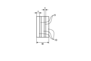
図4は、実施の形態1にかかる電機子2に備えられるコイル7の一部を示す図である。図4では、図3に示す枠IVの部分を拡大して示している。コイル7は、線状の導体10からなる。コイル7を構成する導体10は、コア基板6において渦巻き状にパターニングされている。渦巻きの中心には、導体10が設けられていない空きスペースが設けられている。以下の説明では、コイル7の中心のスペースである空きスペースを、内周部と称する。図3に示す例では、内周部は六角形の領域である。導体10は、内周部に隣接する起点から内周部の周囲を複数回周回させて配置されている。図3に示す例では、コイル7の外形は六角形である。なお、枠IVの部分は、コイル7のうち軸方向に導体10が延ばされている部分である。
FIG. 4 is a diagram showing a part of the
図4に示す例では、導体10は、内周部の周囲を3回周回させて配置されている。図4には、導体10のうち互いに平行な3つの線状部分を示している。コア基板6上において互いに隣り合う線状部分同士の間には、線状部分同士の絶縁のためのスペース9が設けられている。なお、コイル7の平面構成は、図3および図4に示す構成に限られず任意であるものとする。コイル7の外形は六角形以外でも良く、長円形状などでも良い。導体10は、内周部の周囲において3回よりも多く周回させて配置されても良い。
In the example shown in FIG. 4, the
図5は、実施の形態1にかかる電機子2の断面図である。図5に示す断面は、図3に示すV-V線における断面である。図5では、円筒形状に巻かれたプリント基板5の一部の断面を示している。図5における左右方向が周方向に相当し、図5における上下方向が径方向に相当するものとする。図6は、実施の形態1にかかる電機子2の一部を示す図である。図6では、図5に示す枠VIの部分を拡大して示している。
FIG. 5 is a sectional view of the
図5および図6に示す例では、コイル7は、コア基板6の両面に設けられている。図5および図6に示すプリント基板5は、いわゆる「両面実装基板」に該当する。絶縁層11は、径方向に配列されているコイル7同士の間に設けられている。絶縁層11は、例えば、接着性を備える絶縁シートである。絶縁層11は、絶縁性を備える接着シート、または、絶縁性を備える接着剤などでも良い。
In the example shown in FIGS. 5 and 6, the
図5および図6に示す電機子2では、2つのコア基板6の間にコイル7、絶縁層11、およびコイル7が挟み込まれてなる層12が複数積層されている。径方向において積層されているプリント基板5の層12の数を、Nとする。Nは、正の整数とする。以下の説明では、Nを層数とも称する。なお、図5に示す例では、プリント基板5のうち径方向における両端にはコア基板6があるが、当該両端の少なくとも一方には絶縁層11があっても良い。
In the
上記説明では、プリント基板5は「両面実装基板」であるものと説明としたが、これに限られない。プリント基板5は、「片面実装基板」または「多層実装基板」でも良い。「片面実装基板」に該当するプリント基板5では、コア基板6の両面のうちの一方のみにコイル7が実装される。「多層実装基板」に該当するプリント基板5では、コア基板6の上においてコイル7と絶縁層11とが交互に積層される。
In the above description, the printed
実施の形態1において、導体10のうちコイル7を構成する部分は、プリント基板5の上において一定の幅で形成されている。以下の説明では、プリント基板5の上における導体10の幅をxとする。径方向における導体10の厚さをyとする。コイル7のうち図3に示す枠IVの部分の幅をWとする。コイル7のうち当該部分の幅とは、周方向における幅である。以下の説明では、コイル7のうち当該部分の幅であるWを、スロット幅とも称する。周方向におけるスペース9の幅をcとする。周方向におけるスペース9の幅とは、プリント基板5の上のコイル7における導体10同士の間隔ともいえる。径方向におけるコア基板6の厚さをm、および、径方向における絶縁層11の厚さをhとする。各コイル7における内周部の幅をa、および、互いに隣り合うコイル7同士の間の距離をbとする。内周部の幅とは、周方向における幅である。コイル7同士の間の距離とは、周方向における距離である。
In the first embodiment, the portion of the
図7は、実施の形態1にかかる電機子2を製造する工程の例を示す図である。図7には、平面状に広げられた状態で形成されたプリント基板5を巻くことによって、円筒形状のプリント基板5からなる電機子2が形成される様子を模式的に示している。なお、プリント基板5のうち円筒形状内側の面にはコア基板6または絶縁層11があるが、図7では当該面におけるコア基板6または絶縁層11が省略されているものとする。上記説明ではコイル7の外形は六角形であるものとしたが、図7ではコイル7の外形を長円形状に簡略化している。
FIG. 7 is a diagram showing an example of a process for manufacturing the
プリント基板5の構成要素の各々は、プリント基板5が巻かれる際に破壊されないように屈曲性を備えることが求められる。また、プリント基板5の構成要素の各々は、プリント基板5が巻かれることによって絶縁性能などの電気的特性が大きく変化しないことが求められる。なお、電機子2は、プリント基板5を巻くことによって形成されるものに限られない。電機子2は、あらかじめ円筒形状に成形されたコア基板6にコイル7が実装されたものであっても良い。
Each component of the printed
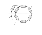
図8は、実施の形態1にかかる電動機1の断面図である。図8に示す断面は、軸方向に垂直な断面であって、軸方向における電機子2の中心における断面である。以下の説明では、電機子2の外径をD、および、電機子2の内径をdとする。外径であるD、および内径であるdは、いずれも直径であるものとする。電機子2におけるコイル7が配置される領域であるスロットの数をn、および、スロット1つ当たりのコイル7の巻数をTとする。電機子2のスロット数は、電動機1の仕様により決定される。
FIG. 8 is a sectional view of the
図9は、実施の形態1にかかる電機子2のスロット数について説明するための第1の図である。図10は、実施の形態1にかかる電機子2のスロット数について説明するための第2の図である。ここでは、複数のコイル7の配置方式が集中巻である場合と複数のコイル7の配置方式が分布巻である場合とにおいて、スロットの数え方を統一する。図9には、集中巻の場合におけるコイル7の配置態様を模式的に示している。図10には、分布巻の場合におけるコイル7の配置態様を模式的に示している。図9および図10では、U相、V相、およびW相の各々についてのコイル7が配置される領域を示す。各領域におけるマークは、コイル7の通電方向を表している。互いに同じマークは、互いに同じ通電方向を表す。互いに異なるマークは、互いに逆の通電方向を表す。
FIG. 9 is a first diagram for explaining the number of slots in the
図9に示す集中巻の場合、周方向において互いに隣り合う2つの領域に、通電方向が互いに逆であるコイル7が配置される。集中巻の場合、当該領域の各々をスロットとする。図9では、1つのスロットの例である領域13を示している。
In the case of concentrated winding shown in FIG. 9, coils 7 whose energization directions are opposite to each other are arranged in two regions adjacent to each other in the circumferential direction. In the case of concentrated winding, each area is a slot. FIG. 9 shows
図10に示す分布巻の場合、通電方向が互いに同じである領域が周方向において隣り合う。各相について、通電方向が互いに逆である2つの領域は、複数の領域を跨いで配置されている。分布巻の場合、当該領域の各々をスロットとする。図10では、1つのスロットの例である領域13を示している。
In the case of the distributed winding shown in FIG. 10, regions in which the current direction is the same are adjacent to each other in the circumferential direction. For each phase, two regions whose energization directions are opposite to each other are arranged across a plurality of regions. In the case of distributed winding, each of the regions is a slot. FIG. 10 shows
次に、幅xと厚さyとを決定する方法の1つである第1の方法について説明する。図11は、実施の形態1にかかる電機子2における導体10の幅とスロットにおける導体10の占積率との関係の例を示す図である。図11では、導体10の幅xと導体10の占積率との関係を表すグラフを示す。図11において、縦軸は占積率を表す。横軸は幅xを表す。プリント基板5の製造上の制約により、導体10の厚さyは、0.03mmから0.12mmまでに包含される厚さとする。図11には、厚さyが0.03mm以上かつ0.12mm以下の範囲における幅xと占積率との関係を表すグラフを示している。
Next, a first method, which is one of the methods for determining the width x and thickness y, will be explained. FIG. 11 is a diagram showing an example of the relationship between the width of the
xおよびyの組には、電機子2のうち周方向に垂直な断面における導体10の占積率を最大にさせる、xであるxoptおよびyであるyoptの組が設定される。図11に示すグラフにおいて占積率が最大となるときのxが、xoptである。yが0.03mmから0.12mmまでに包含される厚さであることから、yoptは、0.03mmから0.12mmまでに包含される厚さである。
A set of x opt and y opt, which maximize the space factor of the
ここで、導体10の幅xと導体10の占積率との関係を表す理論計算式の詳細について説明する。スロット幅Wが決定されることによって幅xを導き出すことができる。スロット幅Wは、プリント基板5の設計諸元により、次の式(1)で表される。
Here, details of a theoretical calculation formula expressing the relationship between the width x of the

また、スロット幅Wは、電機子2の各部寸法により、次の式(2)で表される。
Further, the slot width W is expressed by the following equation (2) depending on the dimensions of each part of the

式(1)と式(2)との組合せから、幅xは次の式(3)で表される。 From the combination of equations (1) and (2), the width x is expressed by the following equation (3).

内周部の幅aについて、集中巻の場合はa=aが式(3)に代入され、分布巻の場合はa=0が式(3)に代入される。 Regarding the width a of the inner peripheral portion, in the case of concentrated winding, a=a is substituted into equation (3), and in the case of distributed winding, a=0 is substituted into equation (3).
導体10の幅xを求める際には、電機子2の層数Nが決定される必要がある。層数Nは、導体10の厚さyが決定されることにより求めることができる。厚さyは、次の式(4)で表される。
When determining the width x of the

上記するように、厚さyは、プリント基板5の製造上の制約により、0.03mm以上かつ0.12mm以下の範囲に包含される厚さである。層数Nは正の整数である。層数Nの値を増減させることで、yの値が0.03mm以上かつ0.12mm以下の範囲に包含されるときの層数Nを求めることができる。厚さyと層数Nとが求まることで、式(3)により幅xを求めることができる。
As described above, the thickness y is within the range of 0.03 mm or more and 0.12 mm or less due to manufacturing constraints of the printed
図12は、実施の形態1にかかる電機子2におけるスロットの断面図である。図13は、図12に示す断面のうち導体10の断面のみを取り出した図である。図12には、1つのスロットである領域13の断面を示している。
FIG. 12 is a sectional view of a slot in the
スロットにおける導体10の断面積Sは、次の式(5)で表される。幅xと厚さyとが決定されることによって、断面積Sを導き出すことができる。
The cross-sectional area S of the

式(3)から式(5)より、層数Nが決定されることによって断面積Sが決定されることが分かる。 From equations (3) to (5), it can be seen that the cross-sectional area S is determined by determining the number of layers N.
断面積Sを最大にさせるときの幅xと厚さyとを導体10に持たせてプリント基板5が形成されることによって、スロットにおける導体10の占積率が最大となる。幅xと厚さyとの組に、導体10の占積率を最大にさせる幅xoptと厚さyoptとの組が設定され、導体10の占積率が最大となることによって、導体10の電気抵抗が小さくなり、導体10の損失が少なくなる。これにより、電動機1は、銅損を低減でき、銅損に起因する発熱を低減できる。
By forming the printed
ここまで、幅xと厚さyとを決定する方法の1つである第1の方法について説明した。次に、幅xと厚さyとを決定する他の方法である第2の方法について説明する。第2の例では、電動機1は、1つ以上の単位構造からなるものとする。ここでは、界磁3に備わる磁極と電機子2におけるコイル7が配置される領域であるスロットとの組であって一定数の磁極と一定数のスロットとの組を、電動機1の単位構造と称する。
Up to this point, the first method, which is one of the methods for determining the width x and thickness y, has been described. Next, a second method, which is another method for determining the width x and thickness y, will be explained. In the second example, the
図14は、実施の形態1にかかる電動機1の単位構造15について説明するための図である。図14には、電機子2のうち1つの単位構造15を構成する部分と、界磁3のうち1つの単位構造15を構成する部分とを模式的に示している。図14における左右方向が周方向に相当し、図14における上下方向が径方向に相当するものとする。電機子2のうち1つの単位構造15を構成する部分において、複数のスロットが周方向に並べられている。図14に示す矩形16は、複数のスロットの1つを表している。界磁3のうち1つの単位構造15を構成する部分において、複数の磁極が周方向に並べられている。図14に示す矩形17は、複数の磁極の1つを表している。
FIG. 14 is a diagram for explaining the
例えば、電動機1の全体における磁極の数が6、かつ、電動機1の全体におけるスロットの数が9とする。この場合、電動機1の単位構造15は2個の磁極と3個のスロットとの組であって、電動機1は3個の単位構造15からなる。なお、単位構造15における磁極の数とスロットの数とは任意であるものとする。また、電動機1が有する単位構造15の数は任意であるものとする。以下の説明では、単位構造15におけるスロットの数をn′、電機子2のうち単位構造15を構成する部分の、周方向における長さをL、および径方向におけるスロットの長さをHとする。
For example, it is assumed that the number of magnetic poles in the entire
第2の方法においても、第1の方法と同様に、スロット幅Wが決定されることによって幅xoptと厚さyoptとの組が導き出される。また、第2の方法においても、式(1)は成立する。 In the second method, as in the first method, the slot width W is determined to derive a set of the width x opt and the thickness y opt . Further, in the second method as well, equation (1) holds true.
スロット幅Wは、電機子2の各部寸法により、次の式(6)で表される。
The slot width W is expressed by the following equation (6) based on the dimensions of each part of the

式(1)と式(6)との組合せから、幅xは次の式(7)で表される。 From the combination of equations (1) and (6), the width x is expressed by the following equation (7).

内周部の幅aについて、集中巻の場合はa=aが式(7)に代入され、分布巻の場合はa=0が式(7)に代入される。 Regarding the width a of the inner peripheral portion, in the case of concentrated winding, a=a is substituted into equation (7), and in the case of distributed winding, a=0 is substituted into equation (7).
厚さyは、次の式(8)で表される。 The thickness y is expressed by the following equation (8).

層数Nの値を増減させることで、yの値が0.03mm以上かつ0.12mm以下の範囲に包含されるときの層数Nを求めることができる。厚さyと層数Nとが求まることで、式(7)により幅xを求めることができる。幅xと厚さyとが決定されることによって、断面積Sを導き出すことができる。 By increasing or decreasing the value of the number of layers N, the number of layers N when the value of y falls within the range of 0.03 mm or more and 0.12 mm or less can be determined. By determining the thickness y and the number N of layers, the width x can be determined using equation (7). By determining the width x and thickness y, the cross-sectional area S can be derived.
断面積Sを最大にさせるときの幅xと厚さyとを導体10に持たせてプリント基板5が形成されることによって、スロットにおける導体10の占積率が最大となる。幅xと厚さyとの組に、導体10の占積率を最大にさせる幅xoptと厚さyoptとの組が設定され、導体10の占積率が最大となることによって、導体10の電気抵抗が小さくなり、導体10の損失が少なくなる。これにより、電動機1は、銅損を低減でき、銅損に起因する発熱を低減できる。
By forming the printed
実施の形態2.
図15は、実施の形態2にかかる電機子2の断面図である。実施の形態2では、実施の形態1とは異なる構成について主に説明する。図15では、円筒形状に巻かれたプリント基板5の一部における断面を示している。図15における左右方向が周方向に相当し、図15における上下方向が径方向に相当するものとする。図15に示す構成は、図5に示す構成と同様である。電機子2のうちスロットである領域の断面は、図6に示す断面と同様である。実施の形態2では、複数のコイル7は、集中巻により配置されているものとする。
FIG. 15 is a sectional view of the
図15に示す構成において、各コイル7における内周部の幅をa′、および、互いに隣り合うコイル7同士の間の距離をb′とする。内周部の幅とは、周方向における幅である。コイル7同士の間の距離とは、周方向における距離である。実施の形態2では、a′およびb′の組には、コイル7の巻線係数を最大にさせる、a′であるa′optおよびb′であるb′optの組が設定される。
In the configuration shown in FIG. 15, the width of the inner circumference of each
電動機1にて発生する銅損は、基本的に、巻線係数kwに反比例することが知られている。巻線係数kwは、電動機1の磁極数と電動機1のスロット数との組合せ、または、電動機1における複数のコイル7の配置方式などによって決定される係数である。三相電動機である電動機1の銅損は、相抵抗Rpと相電流の2乗とに比例する。巻線係数kwが大きいほど、電動機1の誘起電圧は大きい。このため、巻線係数kwが大きいほど、同じトルクを出力するために必要な相電流は小さくなる。
It is known that the copper loss generated in the
ここで、巻線係数kwの逆数の2乗に比例する成分を抽出し、抽出された成分を銅損係数kCuと称する。銅損係数kCuは、次の式(9)で表される。 Here, a component proportional to the square of the reciprocal of the winding coefficient k w is extracted, and the extracted component is referred to as a copper loss coefficient k Cu . The copper loss coefficient k Cu is expressed by the following equation (9).

さらに、巻線係数kwは、短節巻係数kpと比例関係にあることが知られている。短節巻係数kpは、スロットのピッチと磁極のピッチとが互いに異なる場合において鎖交磁束が減少する比率を示す係数である。なお、分布巻係数なども巻線係数kwと比例関係にあるが、ここでは詳細を省略する。 Furthermore, it is known that the winding coefficient k w is in a proportional relationship with the short-pitch winding coefficient k p . The short-pitch winding coefficient k p is a coefficient indicating the rate at which the interlinkage magnetic flux decreases when the slot pitch and the magnetic pole pitch are different from each other. Note that the distributed winding coefficient and the like are also in a proportional relationship with the winding coefficient kw , but the details will be omitted here.
図16は、実施の形態2にかかる電機子2におけるコイル7の配置と巻線係数との関係について説明するための図である。図16に示すグラフにおいて、縦軸は巻線係数kwを表し、横軸はコイル7の電気角θと導体10の幅xとを表す。図16におけるグラフの上には、コイル7の構成を模式的に示している。
FIG. 16 is a diagram for explaining the relationship between the arrangement of the
図15に示す電機子2を有する電動機1の短節巻係数kpは、コイル7の内周位置P1とコイル7の外周位置P2との各々における、コイル7と鎖交する磁束の磁束量から導き出すことができる。内周位置P1とは、コイル7の内周上の位置であって内周部に接する位置とする。外周位置P2とは、コイル7の外周上の位置とする。コイル7における鎖交磁束の磁束量は、内周位置P1と外周位置P2との各々では少なく、内周位置P1と外周位置P2との中間で最大となる。磁石が発生する磁束の磁束量と鎖交磁束の磁束量との比が、短節巻係数kpに相当する。各磁石の磁束量をφmagnet、各スロットにおける鎖交磁束の磁束量の最大値をφn_max、各相のコイル7の内周位置P1における電気角をθ1、および各相のコイル7の外周位置P2における電気角をθ2、として、短節巻係数kpは、次の式(10)で表される。
The short pitch winding coefficient k p of the

電気角θ1は、図15に示す構成より、次の式(11)で表される。電気角θ2は、図15に示す構成より、次の式(12)で表される。電動機1に適用される磁極の数をp、および複数の磁極が配置されるピッチをτpとする。
The electrical angle θ 1 is expressed by the following equation (11) using the configuration shown in FIG. The electrical angle θ 2 is expressed by the following equation (12) using the configuration shown in FIG. The number of magnetic poles applied to the


式(9)から式(12)より、幅a′および距離b′は、それぞれ、銅損係数kCuに関係することが分かる。 From equations (9) to (12), it can be seen that the width a' and the distance b' are each related to the copper loss coefficient kCu .
図17は、実施の形態2にかかる電動機1について、各コイル7における内周部の幅と銅損係数との関係の例を示す図である。図17に示すグラフの縦軸は銅損係数kCuを表す。グラフの横軸は内周部の幅a′を表す。図17には、互いに隣り合うコイル7間の距離b′の値が、0、1、2、および3の各々である場合について、幅a′と銅損係数kCuとの関係を表すグラフを示している。
FIG. 17 is a diagram showing an example of the relationship between the width of the inner peripheral portion of each
図17によると、距離b′の値が小さいほど、銅損係数kCuは小さい。銅損係数kCuが小さいとは、銅損が少ないことを示す。また、図17によると、距離b′が0、1、2、および3のいずれの値である場合も、銅損係数kCuを極小値とさせる幅a′の値が存在する。銅損係数kCuが極小値であるときにおける幅a′と距離b′との組が、コイル7の巻線係数kwを最大にさせるa′optおよびb′optの組である。
According to FIG. 17, the smaller the value of distance b', the smaller the copper loss coefficient k Cu . A small copper loss coefficient k Cu indicates that copper loss is small. Further, according to FIG. 17, when the distance b' is any value of 0, 1, 2, or 3, there exists a value of the width a' that makes the copper loss coefficient k Cu a minimum value. The set of width a' and distance b' when the copper loss coefficient k Cu is the minimum value is the set of a' opt and b' opt that maximizes the winding coefficient k w of the
図17によると、幅a′が0に近づくほど、コイル7のうち磁石に対向する部分の面積が増えて、コイル7の鎖交磁束量が増加する。コイル7の鎖交磁束量が増加すると、短節巻係数kpが大きくなり、銅損係数kCuは小さくなる。幅a′がτp/2程度にまで大きくなると、磁石による磁束の密度が最大である位置にコイル7が存在しなくなるため、短節巻係数kpが大幅に減少することとなる。よって、幅a′optは、次の式(13)を満足することが望ましい。
According to FIG. 17, as the width a' approaches 0, the area of the portion of the
![]()
![]()
幅a′optについての上記説明は、距離b′optの場合においても同様といえる。式(12)において電気角θ2の値が取り得る範囲を考慮し、距離b′optは、次の式(14)を満足することが望ましい。 The above explanation regarding the width a' opt can be said to be the same in the case of the distance b' opt . Considering the possible range of the value of the electrical angle θ 2 in equation (12), it is desirable that the distance b' opt satisfies the following equation (14).

コイル7の巻線係数kwを最大にさせるときの幅a′optおよび距離b′optを満足するように複数のコイル7が形成されることによって、電動機1の銅損が少なくなる。さらに、幅a′optが式(13)を満足し、かつ距離b′optが式(14)を満足することにより、銅損係数kCuを小さくすることができ、電動機1の銅損がさらに少なくなる。これにより、電動機1は、銅損を低減でき、銅損に起因する発熱を低減できる。
Copper loss in the
実施の形態3.
図18は、実施の形態3にかかる電機子2の構成について説明するための第1の図である。図19は、実施の形態3にかかる電機子2の構成について説明するための第2の図である。実施の形態3では、実施の形態1または2とは異なる構成について主に説明する。
FIG. 18 is a first diagram for explaining the configuration of the
図18および図19には、平面状のプリント基板5が円筒形状に巻かれるときの様子を模式的に示している。図18および図19において、コイル部14は、層12のうち絶縁層11を介して積層された2つのコイル7を有する部分を表す。コイル部14は、層12のうちコイル7が形成されている領域であって、スロットを構成する領域といえる。図18および図19では、コア基板6を簡略化して示している。図18および図19では、絶縁層11の図示を省略する。実施の形態3では、複数のコイル7は、集中巻により配置されているものとする。
18 and 19 schematically show how the planar printed
プリント基板5を円筒形状に巻くことによって、N個の層12を有する電機子2が形成される。実施の形態3では、Nは2以上の整数とする。電機子2の各スロットでは、複数のコイル部14が径方向に配列されていることが望ましい。ただし、コア基板6の上における複数のコイル7の全てが一定の距離bで配置されていると、各スロットでは、周方向におけるコイル部14の位置にずれが生じることとなる。コイル部14の位置にずれが生じることで、スロットが、理想とする形状とは異なる形状となる。スロットの理想とする形状とは、スロットにおける各層12のコイル7が径方向に配列されているときの形状である。
By winding the printed
ここで、Mを、1以上かつN未満の整数とする。プリント基板5の複数の層12のうち円筒形状の中心軸AXの方からM番目の層12のうち円筒形状の巻き終わりに最も近いコイル7と、プリント基板5の複数の層12のうち円筒形状の中心軸AXの方から(M+1)番目の層12のうち円筒形状の巻き始めに最も近いコイル7との間の距離をb′′とする。図18および図19では、M番目の層12のうち円筒形状の巻き終わりに最も近いコイル部14と、(M+1)番目の層12のうち円筒形状の巻き始めに最も近いコイル部14との間の距離がb′′であるものとする。距離b′′の長さが、プリント基板5の複数の層12の各々におけるコイル7同士の間の距離bの長さと同じであると、理論上、(M+1)番目の層12のコイル7の位置は、M番目の層12のコイル7に対して周方向にずれた位置となる。
Here, M is an integer greater than or equal to 1 and less than N. Among the plurality of
実施の形態3では、図18に示すように、距離b′′が距離bよりも長くなるようにコア基板6におけるコイル7の位置が決定される。距離b′′が距離bよりも長いことにより、(M+1)番目の層12のコイル7について、M番目の層12のコイル7に対するずれを無くすことができる。すなわち、(M+1)番目の層12のコイル7と、M番目の層12のコイル7とを、径方向に配列させることができる。図19には、図18に示す状態から、コア基板6のうち距離b′′の部分を撓ませることによって、M番目の層12のコイル部14と、(M+1)番目の層12のコイル部14とを径方向に配列させる様子を示している。このように、距離b′′が距離bよりも長くされて、周方向におけるコイル部14の位置が調整されることによって、1つの層12のコイル部14と、当該層12の外周側の層12のコイル部14とを径方向に配列させることができる。径方向において互いに隣り合う層12同士においてコイル部14を径方向に配列させることによって、理想とする形状のスロットを得ることが可能となる。
In the third embodiment, as shown in FIG. 18, the position of the
実施の形態3において、距離b′′は、次の式(15)を満足する。 In the third embodiment, the distance b'' satisfies the following equation (15).

ここで、式(15)を導出する過程について説明する。図20は、実施の形態3にかかる電機子2におけるコイル7の配置について説明するための第1の図である。図21は、実施の形態3にかかる電機子2におけるコイル7の配置について説明するための第2の図である。
Here, the process of deriving equation (15) will be explained. FIG. 20 is a first diagram for explaining the arrangement of the
図20および図21において、コイル部14nMは、プリント基板5の巻き始めからnM番目のコイル部14である。コイル部14nMは、M番目の層12のうち円筒形状の巻き終わりに最も近いコイル部14である。コイル部14nM+1は、プリント基板5の巻き始めから(nM+1)番目のコイル部14である。コイル部14nM+1は、(M+1)番目の層12のうち円筒形状の巻き始めに最も近いコイル部14である。コイル部14n(M-1)+1は、プリント基板5の巻き始めから{n(M-1)+1}番目のコイル部14である。コイル部14n(M-1)+1は、(M-1)番目の層12のうち円筒形状の巻き始めに最も近いコイル部14である。
20 and 21, the
図20には、距離b′′が式(15)を満足する場合であって距離b′′の長さが最も短いケース、すなわち距離b′′の長さが距離bの長さと同じであるケースを示している。この場合、コイル部14nM+1とコイル部14nMとは、中心軸AXを中心とする同じ円の上に配置される。上記説明では、距離b′′の長さが距離bの長さと同じであると、理論上、(M+1)番目の層12のコイル7の位置は、M番目の層12のコイル7に対して周方向にずれた位置となる、とした。ただし、プリント基板5が円筒形状に巻かれることで、円筒形状が径方向に膨れること、または、プリント基板5にかかる張力によりプリント基板5が変形することがあり得る。距離b′′の長さが距離bの長さと同じである場合でも、円筒形状の膨れまたはプリント基板5の変形によって、(M+1)番目の層12のコイル7とM番目の層12のコイル7とが径方向に配列されることがあり得る。このため、式(15)では、距離b′′が距離bに等しい場合が含められている。
FIG. 20 shows a case where the distance b'' satisfies equation (15) and the length of the distance b'' is the shortest, that is, the length of the distance b'' is the same as the length of the distance b. shows the case. In this case, the
図21には、距離b′′が式(15)を満足する場合であって距離b′′の長さが最も長いケースを示している。 FIG. 21 shows a case where the distance b'' satisfies Equation (15) and the length of the distance b'' is the longest.
図22は、実施の形態3にかかる電機子2におけるコイル7の配置について説明するための第3の図である。図23は、実施の形態3にかかる電機子2におけるコイル7の配置について説明するための第4の図である。図24は、実施の形態3にかかる電機子2におけるコイル7の配置について説明するための第5の図である。
FIG. 22 is a third diagram for explaining the arrangement of the
図22には、距離b′′の長さが最も長い場合における、電機子2におけるコイル部14n(M-1)+1,14nM,14nM+1の配置の態様を模式的に示している。式(15)のうち「<」の右側の式は、コイル部14n(M-1)+1とコイル部14nMとが、中心軸AXを中心とする同じ円の上に配置される場合を表す。
FIG. 22 schematically shows the arrangement of the
図23に示す三角形は、図22においてコイル部14n(M-1)+1,14nM+1とコイル部14nMとの間に示す三角形を表す。図23に示す三角形は、距離b′′の長さの第1辺と、距離bの長さの第2辺と、h+yf+2mの長さの第3辺とを有する。図23において、角度θは、第2辺と第3辺とがなす角の角度、すなわち、第1辺の対角の角度である。
The triangle shown in FIG. 23 represents the triangle shown between the
距離b′′は、次の式(16)で表される。 The distance b'' is expressed by the following equation (16).
![]()
![]()
半径rは、中心軸AXを中心とする円の半径であって、各コイル部14n(M-1)+1,14nMが配置される位置を表す円の半径とする。図24に示す角度θ′は、図23に示す三角形の第3辺を中心軸AXの方へ延伸させた場合において現れる角の角度であって、第2辺および第3辺の間の角の補角である。角度θ′は、次の式(17)で表される。
The radius r is the radius of a circle centered on the central axis AX, and represents the position where each
![]()
![]()
中心軸AXと周方向におけるコイル部14n(M-1)+1の中心を通る直線と、中心軸AXと周方向におけるコイル部14nMの中心を通る直線とがなす角度は、2π/nと表される。コイル部14の幅、すなわちスロット幅Wは、半径rを用いて表すことができる。このことから、角度θ′は、次の式(18)で表される。
The angle between the central axis AX and a straight line passing through the center of the

図25は、実施の形態3にかかる電機子2におけるコイル7の配置について説明するための第6の図である。図25には、1つのスロットを構成するN個のコイル部14n1,14n2,・・・,14nM,・・・,14nNを示す。コイル部14n1は、1番目の層12のコイル部14である。コイル部14n2は、2番目の層12のコイル部14である。コイル部14nMは、M番目の層12のコイル部14である。コイル部14nNは、N番目の層12のコイル部14である。1つの層12の径方向長さは、(D-d)/2Nと表される。半径rは、次の式(19)で表される。
FIG. 25 is a sixth diagram for explaining the arrangement of the

式(17)から式(19)を式(16)に代入することで、式(15)のうち「<」の右側の式が得られる。ただし、プリント基板5が円筒形状に巻かれることによる、円筒形状の膨れまたはプリント基板5の変形によって、式(15)のうち「<」の右側の式に距離b′′が等しくなる想定通りの状況とはならないといえる。このため式(15)では、式(15)のうち「<」の右側の式に距離b′′が等しい場合が除かれている。
By substituting equations (17) to (19) into equation (16), the equation on the right side of "<" in equation (15) can be obtained. However, due to the bulge in the cylindrical shape or the deformation of the printed
実施の形態3において、距離b′′が式(15)を満足することによって、径方向において互いに隣り合う層12同士においてコイル部14を径方向に配列させることができる。これにより、理想とする形状のスロットを有する電機子2を得ることが可能となる。
In the third embodiment, when the distance b'' satisfies the expression (15), the
実施の形態4.
図26は、実施の形態4にかかる電機子2の一部の断面図である。図26には、1つのスロットの例である領域13の断面を示している。実施の形態4では、実施の形態1-3とは異なる構成について主に説明する。図26に示す断面は、中心軸AXに垂直な断面である。図26には、N個のコイル部14を示している。実施の形態4では、Nは2以上の整数とする。
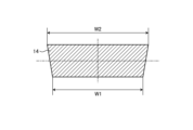
FIG. 26 is a cross-sectional view of a portion of the
電機子2を製造する上で、図26に示す断面におけるスロットの理想的な形状は、台形に近い形状である。実施の形態4では、周方向におけるコイル部14の長さが、円筒形状の内周側よりも円筒形状の外周側のほうが長いことにより、スロットが理想的な形状に近い形状とされている。
In manufacturing the
図27は、実施の形態4にかかる電機子2におけるコイル部14の断面図である。図27に示す断面は、中心軸AXに垂直な断面である。
FIG. 27 is a sectional view of the
層12におけるコイル7が形成されている領域であるコイル部14のうち中心軸AXの方の端の、周方向における幅をW1、およびコイル部14のうち中心軸AXとは逆の方の端の、周方向における幅をW2、とする。W1およびW2は、次の式(20)を満足する。
The width in the circumferential direction of the end of the

スロットを構成する各コイル部14では、幅W2のほうが幅W1よりも0%から5%程度長い。これにより、台形に近い理想的な形状のスロットを得ることができる。スロットを理想的な形状とすることによって、電機子2を製造する際における電機子2の形状の崩れを低減できる。
In each
実施の形態5.
図28は、実施の形態5にかかる電機子2におけるコイル部14の断面図である。図28に示す断面は、中心軸AXに垂直な断面である。実施の形態5では、実施の形態1-4とは異なる構成について主に説明する。
FIG. 28 is a sectional view of the
層12におけるコイル7が形成されている領域であるコイル部14のうち中心軸AXの方の端の、周方向における幅をW1、コイル部14のうち中心軸AXとは逆の方の端の、周方向における幅をW2、およびコイル部14のうち径方向における中心の、周方向における幅をW3とする。W1およびW3は、次の式(21)を満足する。W2およびW3は、次の式(22)を満足する。
The width in the circumferential direction of the end of the


幅W3は、周方向におけるコイル部14の幅の代表といえる。代表である幅W3よりも幅W1が短く、かつ代表である幅W3よりも幅W2が長いことにより、台形に近い理想的な形状のスロットを得ることができる。スロットを理想的な形状とすることによって、電機子2を製造する際における電機子2の形状の崩れを低減できる。
The width W3 can be said to be representative of the width of the
実施の形態6.
図29は、実施の形態6にかかる電機子2を構成するプリント基板5の模式図である。実施の形態6では、実施の形態1-5とは異なる構成について主に説明する。実施の形態6において、コア基板6の一方の面には、径方向に立てられたピン21が設けられている。コア基板6の他方の面には、孔22が形成されている。孔22は、ピン21を嵌め合わせ可能な形状である。図29には、コア基板6のうち2つのコイル7と1つのピン21と1つの孔22とが設けられている部分を示している。ピン21と孔22とは、コア基板6のうちコイル7が形成されている領域以外の領域に設けられている。
FIG. 29 is a schematic diagram of the printed
プリント基板5が円筒形状に巻かれる際に、スロットを構成するコイル7の配置誤差を低減できることで、スロットを理想的な形状に近づけることができる。実施の形態6では、プリント基板5が巻かれて複数の層12が積層される際に、孔22にピン21が嵌め合わせられる。ピン21と孔22との位置関係は、プリント基板5が巻かれて複数の層12が積層される際に、孔22にピン21を嵌め合わせ可能に設定されている。コア基板6には、コイル7が形成される領域に対して軸方向の位置に、ピン21と孔22とを設けるための領域が確保されている。これにより、プリント基板5が周方向において長くなることが防がれ、占積率を低下させることなくピン21と孔22とを設けることができる。
When the printed
ピン21の径方向長さは、コイル7の厚さyよりも長い。孔22の径方向深さは、ピン21の径方向長さと厚さyとの差分よりも深い。なお、ピン21の形状は、図29に示す円柱形状に限られない。ピン21の形状は、コイル7の配置誤差を低減可能な形状であれば良く、軸方向または周方向を長手方向とする長円柱形状などでも良い。孔22は、ピン21の形状に合わせた形状とされる。ピン21と孔22との位置関係は、コイル7の配置誤差を低減可能なものであれば良い。ピン21の位置に対して、孔22の位置が軸方向または周方向にずれた位置であっても良い。
The radial length of the
ピン21の材質は、任意とする。ピン21の材質は、プリント基板5の構成部品の1つと同じ材質により形成されても良く、プリント基板5の構成部品には使用されていない材質により形成されても良い。ピン21は、プリント基板5の構成部品が実装されるときに接合されても良く、プリント基板5の構成部品が実装された後に追加されても良い。
The material of the
電機子2が製造される際においてピン21が孔22に嵌め合わせられることによって、スロットを構成するコイル7の配置誤差を低減できる。これにより、電動機1の性能低下を防ぐことができる。
By fitting the
実施の形態7.
図30は、実施の形態7にかかる電機子2を構成するプリント基板5の模式図である。実施の形態7では、実施の形態1-6とは異なる構成について主に説明する。実施の形態7において、複数のコイル7は、コア基板6の一方の面に設けられている。コア基板6の他方の面には、コイル7を嵌め合わせ可能な形状の凹部23が形成されている。図30には、コア基板6のうち2つのコイル7と2つの凹部23とが設けられている部分を示している。
FIG. 30 is a schematic diagram of a printed
実施の形態7では、プリント基板5が巻かれて複数の層12が積層される際に凹部23にコイル7が嵌め合わせられる。凹部23は、コイル7の形状に合わせた形状とされている。凹部23の位置は、プリント基板5が巻かれて複数の層12が積層される際に、凹部23にコイル7を嵌め合わせ可能に設定されている。
In the seventh embodiment, the
電機子2が製造される際においてコイル7が凹部23に嵌め合わせられることによって、スロットを構成するコイル7の配置誤差を低減できる。これにより、電動機1の性能低下を防ぐことができる。実施の形態7では、実施の形態6と比べて、コア基板6のうちコイル7と接する部分の面積が大きい。このため、実施の形態7では、実施の形態6と比べて、積層された層12の間における熱伝達率が向上する。電動機1は、積層された層12の間における熱伝達率が向上することで、通電時におけるコイル7の温度上昇を低減させることができる。
By fitting the
実施の形態8.
図31は、実施の形態8にかかる電機子2を構成するプリント基板5の概略構成を示す図である。実施の形態8では、実施の形態1-7とは異なる構成について主に説明する。図31では、円筒形状のプリント基板5を平面状に展開した場合におけるプリント基板5の一部を示している。
FIG. 31 is a diagram showing a schematic configuration of a printed
実施の形態8では、複数の層12において、周方向におけるコイル7の位置が層12ごとにずれている。かかる構成により、径方向において互いに隣り合うコイル7では、コイル7の電気角が互いに異なる。図31では、1つの層12に設けられているコイル7を示している。図31では、参考として、当該1つの層12の紙面奥側に配置される層12のコイル7を破線で示している。
In
図32は、実施の形態8にかかる電機子2の一部の断面図である。図32には、1つのスロットの例である領域13の断面を示している。図32に示す断面は、中心軸AXに垂直な断面である。図32における左右方向が周方向に相当し、図32における上下方向が軸方向に相当するものとする。図32に示すように、径方向における位置ごとに、周方向におけるコイル7の位置がずれている。プリント基板5では、径方向における位置ごとに、周方向におけるコイル7の位置がずれるように、複数のコイル7が実装されている。
FIG. 32 is a cross-sectional view of a part of the
周方向におけるコイル7の位置が層12ごとにずれていることによって、いわゆるスキューが施された電機子2を形成可能である。これにより、電動機1は、電動機1の駆動方向におけるトルクリップル、または電動機1の駆動方向における推力リップルを低減させることができる。
By shifting the positions of the
以上の各実施の形態に示した構成は、本開示の内容の一例を示すものである。各実施の形態の構成は、別の公知の技術と組み合わせることが可能である。各実施の形態の構成同士が適宜組み合わせられても良い。本開示の要旨を逸脱しない範囲で、各実施の形態の構成の一部を省略または変更することが可能である。 The configurations shown in each of the above embodiments are examples of the contents of the present disclosure. The configuration of each embodiment can be combined with other known techniques. The configurations of each embodiment may be combined as appropriate. It is possible to omit or change a part of the configuration of each embodiment without departing from the gist of the present disclosure.
1 電動機、2 電機子、3 界磁、4 シャフト、5 プリント基板、6 コア基板、7 コイル、8 渡り配線、9 スペース、10 導体、11 絶縁層、12 層、13 領域、14,14n1,14n2,14n(M-1)+1,14nM,14nM+1,14nN コイル部、15 単位構造、16,17 矩形、21 ピン、22 孔、23 凹部、AX 中心軸。 1 electric motor, 2 armature, 3 field, 4 shaft, 5 printed circuit board, 6 core board, 7 coil, 8 crossover wiring, 9 space, 10 conductor, 11 insulating layer, 12 layer, 13 area, 14, 14 n1 , 14 n2 , 14 n(M-1)+1 , 14 nM , 14 nM+1 , 14 nN coil part, 15 unit structure, 16, 17 rectangle, 21 pin, 22 hole, 23 recess, AX central axis.
Claims (12)
前記電機子に対し前記円筒形状の中心軸の方に配置されている界磁と、を備え、
前記プリント基板は、前記円筒形状の周方向に並べられた複数のコイルを有し、
複数の前記コイルの各々は、線状の導体からなり、
前記プリント基板の上における前記導体の幅をx、および前記径方向における前記導体の厚さをy、として、
前記電機子において前記径方向に積層される前記層の数には、あらかじめ設定された範囲に前記yの値が包含されるときの前記層の数が決定され、
前記電機子における前記コイルが配置される領域であるスロットのうち前記周方向に垂直な断面における、前記導体の断面積をSとして、
決定された数の前記層が積層されてなる前記電機子において、前記xおよび前記yの組には、前記Sの値を最大にさせる、前記xであるxoptおよび前記yであるyoptの組が設定される
ことを特徴とする電動機。 an armature comprising a cylindrical printed circuit board, and a plurality of layers of the printed circuit board are stacked in a radial direction of the cylindrical shape;
a field arranged toward the central axis of the cylindrical shape with respect to the armature;
The printed circuit board has a plurality of coils arranged in the circumferential direction of the cylindrical shape,
Each of the plurality of coils is made of a linear conductor,
The width of the conductor on the printed circuit board is x, and the thickness of the conductor in the radial direction is y,
The number of layers laminated in the radial direction in the armature is determined by the number of layers when the value of y is included in a preset range,
S is the cross-sectional area of the conductor in a cross section perpendicular to the circumferential direction of the slot in the armature where the coil is arranged,
In the armature in which a determined number of the layers are laminated, the set of x and y includes the x opt and the y opt , which maximize the value of S. An electric motor characterized in that a pair is set.
前記プリント基板の上の前記コイルにおける導体同士の間隔をc、前記プリント基板の層ごとに形成されている前記導体の数をf、前記径方向における前記コア基板の厚さをh、前記径方向における前記絶縁層の厚さをm、前記電機子における前記コイルが配置される領域であるスロットの数をn、スロット1つ当たりの前記コイルの巻数をT、前記電機子において前記径方向に積層されている前記プリント基板の層の数をN、前記電機子の外径をD、前記電機子の内径をd、および前記コイルの中心のスペースである内周部の、前記径方向における幅をa、として、
前記xoptは、次の式(1)を満足し、
前記yoptは、次の式(2)を満足する
ことを特徴とする請求項1に記載の電動機。


The distance between the conductors in the coil on the printed circuit board is c, the number of conductors formed in each layer of the printed circuit board is f, the thickness of the core board in the radial direction is h, and the radial direction is m is the thickness of the insulating layer in the armature, n is the number of slots in the armature where the coil is arranged, T is the number of turns of the coil per slot, and lamination in the radial direction in the armature. The number of layers of the printed circuit board is N, the outer diameter of the armature is D, the inner diameter of the armature is d, and the width in the radial direction of the inner peripheral part, which is the space at the center of the coil. a, as,
The x opt satisfies the following formula (1),
The electric motor according to claim 1, wherein the y opt satisfies the following equation (2).
前記プリント基板は、複数の前記コイルが形成されているコア基板と、複数の前記層においてコイル同士の間に設けられている絶縁層と、を備え、
前記プリント基板の上の前記コイルにおける導体同士の間隔をc、前記プリント基板の層ごとに形成されている前記導体の数をf、前記径方向における前記コア基板の厚さをh、前記径方向における前記絶縁層の厚さをm、前記単位構造における前記スロットの数をn′、スロット1つ当たりの前記コイルの巻数をT、前記電機子において前記径方向に積層されている前記プリント基板の層の数をN、前記電機子のうち前記単位構造を構成する部分の、前記周方向における長さをL、前記径方向における前記スロットの長さをH、および前記コイルの中心のスペースである内周部の、前記径方向における幅をa、として、
前記xoptは、次の式(3)を満足し、
前記yoptは、次の式(4)を満足する
ことを特徴とする請求項1に記載の電動機。


The printed circuit board includes a core board on which a plurality of the coils are formed, and an insulating layer provided between the coils in the plurality of layers,
The distance between the conductors in the coil on the printed circuit board is c, the number of conductors formed in each layer of the printed circuit board is f, the thickness of the core board in the radial direction is h, and the radial direction is m is the thickness of the insulating layer in the unit structure, n' is the number of slots in the unit structure, T is the number of turns of the coil per slot, and is the thickness of the printed circuit board laminated in the radial direction in the armature. The number of layers is N, the length in the circumferential direction of the portion of the armature that constitutes the unit structure is L, the length of the slot in the radial direction is H, and the space at the center of the coil. The width of the inner circumference in the radial direction is a,
The x opt satisfies the following formula (3),
The electric motor according to claim 1, wherein the y opt satisfies the following equation (4).
ことを特徴とする請求項1から3のいずれか1つに記載の電動機。 The electric motor according to any one of claims 1 to 3, wherein the y opt has a thickness ranging from 0.03 mm to 0.12 mm.
前記コイルの中心のスペースである内周部の、前記径方向における幅をa′、および互いに隣り合うコイル同士の間の距離をb′、として、
前記a′および前記b′の組には、前記コイルの巻線係数を最大にさせる、前記a′であるa′optおよび前記b′であるb′optの組が設定される
ことを特徴とする請求項2または3に記載の電動機。 The plurality of coils are arranged by concentrated winding,
The width in the radial direction of the inner circumference, which is the space at the center of the coil, is a', and the distance between adjacent coils is b',
The set of a' and b' is set to a set of a', which is a', and b' opt , which maximizes the winding coefficient of the coil. The electric motor according to claim 2 or 3 .
前記a′optは、次の式(5)を満足し、
前記b′optは、次の式(6)を満足する
ことを特徴とする請求項5に記載の電動機。

The a′ opt satisfies the following formula (5),
The electric motor according to claim 5, wherein the b'opt satisfies the following equation (6).
Mを1以上かつ前記N未満の整数として、前記プリント基板の複数の前記層のうち前記円筒形状の前記中心軸の方からM番目の前記層のうち前記円筒形状の巻き終わりに最も近い前記コイルと、前記プリント基板の複数の前記層のうち前記円筒形状の前記中心軸の方からM+1番目の前記層のうち前記円筒形状の巻き始めに最も近い前記コイルとの間の距離をb′′、前記プリント基板の複数の前記層の各々におけるコイル同士の間の距離をb、および前記周方向における前記スロットの幅をW、として、
前記b′′は、次の式(7)を満足する
ことを特徴とする請求項2または3に記載の電動機。

The coil closest to the winding end of the cylindrical shape among the M-th layer from the central axis of the cylindrical shape among the plurality of layers of the printed circuit board, where M is an integer greater than or equal to 1 and less than the N. and the distance between the coil closest to the winding start of the cylindrical shape among the M+1th layer from the central axis of the cylindrical shape among the plurality of layers of the printed circuit board, b'', The distance between the coils in each of the plurality of layers of the printed circuit board is b, and the width of the slot in the circumferential direction is W,
The electric motor according to claim 2 or 3, wherein the b'' satisfies the following equation (7).
前記W1および前記W2は、次の式(8)を満足する
ことを特徴とする請求項7に記載の電動機。

The electric motor according to claim 7, wherein the W1 and the W2 satisfy the following equation (8).
前記W1および前記W3は、次の式(9)を満足し、
前記W2および前記W3は、次の式(10)を満足する
ことを特徴とする請求項7に記載の電動機。


The W1 and the W3 satisfy the following formula (9),
The electric motor according to claim 7 , wherein the W2 and the W3 satisfy the following equation (10).
前記コア基板の一方の面には、前記径方向に立てられたピンが設けられており、
前記コア基板の他方の面には、前記ピンを嵌め合わせ可能な形状の孔が形成されている
ことを特徴とする請求項1から3のいずれか1つに記載の電動機。 The printed circuit board includes a core board on which a plurality of the coils are formed,
A pin erected in the radial direction is provided on one surface of the core board,
The electric motor according to any one of claims 1 to 3 , wherein a hole having a shape into which the pin can be fitted is formed on the other surface of the core board.
複数の前記コイルは、前記コア基板の一方の面に設けられており、
前記コア基板の他方の面には、前記コイルを嵌め合わせ可能な形状の凹部が形成されている
ことを特徴とする請求項1から3のいずれか1つに記載の電動機。 The printed circuit board includes a core board on which a plurality of the coils are formed,
The plurality of coils are provided on one surface of the core substrate,
The electric motor according to any one of claims 1 to 3 , wherein the other surface of the core substrate is formed with a recessed portion having a shape into which the coil can be fitted.
ことを特徴とする請求項1から3のいずれか1つに記載の電動機。 The electric motor according to any one of claims 1 to 3 , wherein in the plurality of layers, the position of the coil in the circumferential direction is shifted from layer to layer.
Applications Claiming Priority (1)
| Application Number | Priority Date | Filing Date | Title |
|---|---|---|---|
| PCT/JP2023/026448 WO2025017881A1 (en) | 2023-07-19 | 2023-07-19 | Electric motor |
Publications (3)
| Publication Number | Publication Date |
|---|---|
| JP7446552B1 true JP7446552B1 (en) | 2024-03-08 |
| JPWO2025017881A1 JPWO2025017881A1 (en) | 2025-01-23 |
| JPWO2025017881A5 JPWO2025017881A5 (en) | 2025-06-24 |
Family
ID=90105476
Family Applications (1)
| Application Number | Title | Priority Date | Filing Date |
|---|---|---|---|
| JP2023579130A Active JP7446552B1 (en) | 2023-07-19 | 2023-07-19 | Electric motor |
Country Status (5)
| Country | Link |
|---|---|
| US (1) | US20260121473A1 (en) |
| JP (1) | JP7446552B1 (en) |
| DE (1) | DE112023006292T5 (en) |
| TW (1) | TWI882854B (en) |
| WO (1) | WO2025017881A1 (en) |
Citations (4)
| Publication number | Priority date | Publication date | Assignee | Title |
|---|---|---|---|---|
| JPS6032533A (en) * | 1983-07-30 | 1985-02-19 | Osada Denki Kogyo Kk | Sheet coil for cylindrical motor |
| WO2018193618A1 (en) * | 2017-04-21 | 2018-10-25 | 三菱電機株式会社 | Coil body, stator, rotating machine, and coil body manufacturing method |
| JP2020114100A (en) * | 2019-01-11 | 2020-07-27 | イビデン株式会社 | Coil substrate for motor and motor |
| JP2023022416A (en) * | 2021-08-03 | 2023-02-15 | イビデン株式会社 | Coil substrate, motor coil substrate, and motor |
Family Cites Families (4)
| Publication number | Priority date | Publication date | Assignee | Title |
|---|---|---|---|---|
| JP6475740B2 (en) * | 2014-08-29 | 2019-02-27 | 株式会社Fuji | Working head unit, mounting apparatus, and working head unit control method |
| JP6965683B2 (en) * | 2017-10-17 | 2021-11-10 | 住友金属鉱山株式会社 | Can roll and long substrate processing equipment |
| JP2020089207A (en) | 2018-11-30 | 2020-06-04 | イビデン株式会社 | Motor coil substrate and motor |
| JP7544326B2 (en) * | 2020-02-20 | 2024-09-03 | ニデックアドバンスドモータ株式会社 | Circuit board and motor |
-
2023
- 2023-07-19 US US19/489,616 patent/US20260121473A1/en active Pending
- 2023-07-19 JP JP2023579130A patent/JP7446552B1/en active Active
- 2023-07-19 DE DE112023006292.7T patent/DE112023006292T5/en active Pending
- 2023-07-19 WO PCT/JP2023/026448 patent/WO2025017881A1/en active Pending
-
2024
- 2024-07-04 TW TW113125083A patent/TWI882854B/en active
Patent Citations (4)
| Publication number | Priority date | Publication date | Assignee | Title |
|---|---|---|---|---|
| JPS6032533A (en) * | 1983-07-30 | 1985-02-19 | Osada Denki Kogyo Kk | Sheet coil for cylindrical motor |
| WO2018193618A1 (en) * | 2017-04-21 | 2018-10-25 | 三菱電機株式会社 | Coil body, stator, rotating machine, and coil body manufacturing method |
| JP2020114100A (en) * | 2019-01-11 | 2020-07-27 | イビデン株式会社 | Coil substrate for motor and motor |
| JP2023022416A (en) * | 2021-08-03 | 2023-02-15 | イビデン株式会社 | Coil substrate, motor coil substrate, and motor |
Also Published As
| Publication number | Publication date |
|---|---|
| DE112023006292T5 (en) | 2026-03-12 |
| TW202505947A (en) | 2025-02-01 |
| US20260121473A1 (en) | 2026-04-30 |
| JPWO2025017881A1 (en) | 2025-01-23 |
| WO2025017881A1 (en) | 2025-01-23 |
| TWI882854B (en) | 2025-05-01 |
Similar Documents
| Publication | Publication Date | Title |
|---|---|---|
| US9118224B2 (en) | Stator for rotary electric machine | |
| US8581460B2 (en) | Armature for rotating electrical machine | |
| JP5532319B2 (en) | Stator for rotating electric machine and method for manufacturing the same | |
| JP4583798B2 (en) | Coil for rotating electrical machine, rotating electrical machine, and method for manufacturing coil | |
| JP5488421B2 (en) | Rotating electric machine stator | |
| JP4623129B2 (en) | Rotating electric machine stator and rotating electric machine | |
| JP2005160143A (en) | Rotating electric machine stator | |
| JP4624421B2 (en) | Permanent magnet synchronous machine with rectangular wire winding | |
| JP7805698B2 (en) | Axial gap motor | |
| CN105612679A (en) | Rotating electric machine and manufacturing method thereof | |
| JP2015116108A (en) | Rotary electric machine | |
| JP6598736B2 (en) | Rotating electric machine stator | |
| JP2006067756A (en) | Stator for rotating electrical machine and method for manufacturing stator for rotating electrical machine | |
| JP2020171096A (en) | Stator | |
| JP5072502B2 (en) | Rotating motor | |
| JP7446552B1 (en) | Electric motor | |
| JP2011234443A (en) | Coil and armature | |
| JP2014050236A (en) | Rotary electric machine | |
| JP5057144B2 (en) | Rotating electric machine stator | |
| JP6968215B2 (en) | Rotating machine | |
| WO2024009375A1 (en) | Coil substrate for actuators, and actuator | |
| JP5704418B2 (en) | Rotating electric machine stator | |
| JP7222293B2 (en) | stator | |
| JP2018129975A (en) | Rotary electric machine, and manufacturing method and manufacturing device for tortoiseshell-shaped coil | |
| JP2002034229A (en) | Coreless linear motor |
Legal Events
| Date | Code | Title | Description |
|---|---|---|---|
| A521 | Request for written amendment filed |
Free format text: JAPANESE INTERMEDIATE CODE: A523 Effective date: 20231222 |
|
| A621 | Written request for application examination |
Free format text: JAPANESE INTERMEDIATE CODE: A621 Effective date: 20231222 |
|
| A871 | Explanation of circumstances concerning accelerated examination |
Free format text: JAPANESE INTERMEDIATE CODE: A871 Effective date: 20231222 |
|
| TRDD | Decision of grant or rejection written | ||
| A01 | Written decision to grant a patent or to grant a registration (utility model) |
Free format text: JAPANESE INTERMEDIATE CODE: A01 Effective date: 20240130 |
|
| A61 | First payment of annual fees (during grant procedure) |
Free format text: JAPANESE INTERMEDIATE CODE: A61 Effective date: 20240227 |
|
| R150 | Certificate of patent or registration of utility model |
Ref document number: 7446552 Country of ref document: JP Free format text: JAPANESE INTERMEDIATE CODE: R150 |